Monte Carlo Simulation of Roughening During Thin Film...
93
Monte Carlo Simulation of Roughening During Thin Film Plasma Etching by Angelikopoulos Panagiotis B.A. (National Technical University of Athens) 2004 A dissertation submitted in partial satisfaction of the requirements for the degree of Master of Philosophy in Applied Mathematics in the GRADUATE DIVISION of the NATIONAL TECHNICAL UNIVERSITY OF ATHENS, ZOGRAFOU The thesis work was conducted in the Institute of Microelectronics of the National Centre for Scientific Research Demokritos. Committee in charge: Director of Researcher Evangelos Gogolides, NSCR Demokritos, Chair Vassilios Konstantoudis,PhD NSCR Demokritos Georgios Kokkoris,PhD NSCR Demokritos Fall 2006
Transcript of Monte Carlo Simulation of Roughening During Thin Film...
Monte Carlo Simulation of Roughening During Thin Film Plasma
Etching
by
Angelikopoulos Panagiotis
B.A. (National Technical University of Athens) 2004
A dissertation submitted in partial satisfaction of the
requirements for the degree of
Master of Philosophy
in
Applied Mathematics
in the
GRADUATE DIVISION
of the
NATIONAL TECHNICAL UNIVERSITY OF ATHENS, ZOGRAFOU
The thesis work was conducted in the Institute of Microelectronics of theNational Centre for Scientific Research Demokritos.
Committee in charge:Director of Researcher Evangelos Gogolides, NSCR Demokritos, Chair
Vassilios Konstantoudis,PhD NSCR DemokritosGeorgios Kokkoris,PhD NSCR Demokritos
Fall 2006

The dissertation of Angelikopoulos Panagiotis is approved:
Chair Date
Date
Date
National Technical University, Zografou
Fall 2006

Monte Carlo Simulation of Roughening During Thin Film Plasma
Etching
Copyright 2006
by
Angelikopoulos Panagiotis
1
Abstract
Monte Carlo Simulation of Roughening During Thin Film Plasma Etching
by
Angelikopoulos Panagiotis
Master of Philosophy in Applied Mathematics
National Technical University of Athens, Zografou
Director of Researcher Evangelos Gogolides, NSCR Demokritos, Chair
Director of Researcher Evangelos Gogolides,NSCR DemokritosThesis Committee Chair

i
This thesis is dedicated to evi and myself, the only people that truly helped me in
my quest...
ii
Contents
List of Figures iv
List of Tables vii
I The Importance of Surface roughness 1
1 Introduction 2
1.1 Nanostructure Fabrication . . . . . . . . . . . . . . . . . . . . . . . . . . . . 21.2 Plasma Etching . . . . . . . . . . . . . . . . . . . . . . . . . . . . . . . . . . 4
1.2.1 Mechanisms of Plasma Etching . . . . . . . . . . . . . . . . . . . . . 91.2.2 Reactive Ion Etching . . . . . . . . . . . . . . . . . . . . . . . . . . . 10
1.3 Roughness in thin film technologies . . . . . . . . . . . . . . . . . . . . . . . 12
2 Roughness Characterizations 14
2.0.1 Types of rough surfaces . . . . . . . . . . . . . . . . . . . . . . . . . 142.1 Roughness Parameters . . . . . . . . . . . . . . . . . . . . . . . . . . . . . . 16
2.1.1 Surface Statistical Functions . . . . . . . . . . . . . . . . . . . . . . 172.1.2 Scaling of the Interface Width for Self Affine and Self Similar Surfaces 172.1.3 Anomalous roughening . . . . . . . . . . . . . . . . . . . . . . . . . . 202.1.4 Scaling of the Interface Width for Mounded Surfaces . . . . . . . . . 22
3 Previous Work 24
3.1 Thesis Goals . . . . . . . . . . . . . . . . . . . . . . . . . . . . . . . . . . . 30
II Monte Carlo Simulation 31
3.2 Description of the the simulation method . . . . . . . . . . . . . . . . . . . 32
4 Dry isotropic etching using reactive neutrals 37
4.1 Shadowing Effect . . . . . . . . . . . . . . . . . . . . . . . . . . . . . . . . . 374.2 First order Re-emission . . . . . . . . . . . . . . . . . . . . . . . . . . . . . 424.3 Mixed order Re-emission . . . . . . . . . . . . . . . . . . . . . . . . . . . . . 49
iii
5 Ion enchanced etching 54
5.1 IN ration 1:100 . . . . . . . . . . . . . . . . . . . . . . . . . . . . . . . . . . 555.2 IN ration 2:100 . . . . . . . . . . . . . . . . . . . . . . . . . . . . . . . . . . 555.3 IN ration 5:100 . . . . . . . . . . . . . . . . . . . . . . . . . . . . . . . . . . 555.4 IN ration 10:100 . . . . . . . . . . . . . . . . . . . . . . . . . . . . . . . . . 55
6 An Etching model using Inhibitors 60
6.1 Recipe Number 1 . . . . . . . . . . . . . . . . . . . . . . . . . . . . . . . . . 686.2 Recipe Number 2 . . . . . . . . . . . . . . . . . . . . . . . . . . . . . . . . . 696.3 Recipe Number 3 . . . . . . . . . . . . . . . . . . . . . . . . . . . . . . . . . 71
7 Conclusions 74
Bibliography 75
A Some Ancillary Stuff 81
iv
List of Figures
1.1 Plot of chip size in mm2 vs. lithographic generation. These are best guess estimates. The
point to note is that die that can be expected fill the litho field size (800 mm x 800 mm). 21.2 Photolithography process flow. . . . . . . . . . . . . . . . . . . . . . . . . . . . . 41.3 Types of plasma etching([37]). . . . . . . . . . . . . . . . . . . . . . . . . . . 51.4 Mechanisms of surface etching([10]). . . . . . . . . . . . . . . . . . . . . . . 81.5 Process taking place during plasma etching([37]). . . . . . . . . . . . . . . . 91.6 A discriptive schematic of plasma gas-phase and surface reactions([10]). . . 111.7 This graph of printable line width estimate vs litho wavelength shows that particles as
small as 250 nm could become critical defects. As line width decreases, more layers become
critical, and cleaner the tool and the fabricators have to become. . . . . . . . . . . . . 13
2.1 Example of a rough surface and its 2d projection produced by a linescan as the result of
an the etching of a silicon wafer in SF6 plasma. . . . . . . . . . . . . . . . . . . . . 152.2 Example of a mounded surface.Note the characteristic spacing unit ζ. . . . . . . . . . 162.3 Example of a rough surface with dual morphology produced by the etching of a silicon
wafer in SF6 plasma. . . . . . . . . . . . . . . . . . . . . . . . . . . . . . . . . . 162.4 An illustration of the dependence of the interface width on the length scale
used to measure the surface roughness .At very small length scales, the ap-parent rms height is small, but the measured interface width increaseas asthe length scale expands until it achieves a saturation value determined bythe fact that the variations in the surface are finite. . . . . . . . . . . . . . . 18
2.5 A log-log plot of the surface height-height correlation function for a self affinesurface. The interface width w , the correlation length ξ , and the roughnessexponent α are indicated by the dashed lines [9] . . . . . . . . . . . . . . . . 19
2.6 A log log plot of the saturation value ξ versus the surface dimension . . . . 202.7 Power spectral density behaviour vs exposure time. The times are from the
uppermost curve in descending order:600s,240s,120s,30s,[47] . . . . . . . . . 22
3.1 The ballistic-like deposition model of two kinds of particle. The circles rep-resent the falling particles (particle A or particle C), the squares representparticle A and the squares with a cross denote particle C. The vertical ar-rows show the falling direction and the right and left pointing arrows showthe positions where the falling particles may stick. . . . . . . . . . . . . . . 29

v
3.2 Cosine propability distribution function. . . . . . . . . . . . . . . . . . . . . . . . 343.3 Overhang occuring during etching simulation. . . . . . . . . . . . . . . . . . . . . . 343.4 Monte Carlo procedure for modelling of etching or deposition processes. . . 353.5 view of a typical lattice outpute . . . . . . . . . . . . . . . . . . . . . . . . . 36
4.1 Shadowing effect . . . . . . . . . . . . . . . . . . . . . . . . . . . . . . . . . 384.2 Surface Width vs Time for Shadowing Etching . . . . . . . . . . . . . . . . 384.3 Profile of the wafer,under shadowing etching,etched for 106 particles . . . . 394.4 Etched depth of the wafer,under shadowing etching . . . . . . . . . . . . . . 404.5 hhcf evolution during shadowing etching. . . . . . . . . . . . . . . . . . . . 404.6 Surface fractal parameters evolution under shadowing etching. . . . . . . . . 414.7 Surface Width vs Time for Shadowing Etching . . . . . . . . . . . . . . . . 424.8 illustration of a reemitted particle . . . . . . . . . . . . . . . . . . . . . . . 434.9 Example of the calculation of the surface normal from the discrete surface. 444.10 Profile of the 2D etched surface.s0 = 0.05, s1 = 1.00.Times are increased by
106 particles . . . . . . . . . . . . . . . . . . . . . . . . . . . . . . . . . . . . 454.11 Etched Depth of the 2D etched surface.s0 = 0.05, s1 = 1.00. . . . . . . . . . 454.12 Heights distribution for the final profile after 8 · 106 particles.s0 = 0.05, s1 =
1.00. . . . . . . . . . . . . . . . . . . . . . . . . . . . . . . . . . . . . . . . . 464.13 Rms for various first sticking coefficients,no overhangs . . . . . . . . . . . . 464.14 Rms for various first sticking coefficients,including overhangs . . . . . . . . 474.15 Rms for various first sticking coefficients,no overhangs.The second in always
assumed unity. Note that when we decrease the first sticking coefficient, therms increases more quickly but it still remains linear. . . . . . . . . . . . . . 48
4.16 Height Height Correlation Functions,no overhangs.Time evolves per 106 par-ticles. . . . . . . . . . . . . . . . . . . . . . . . . . . . . . . . . . . . . . . . 49
4.17 Height Height Correlation Functions,no overhangs.[9] . . . . . . . . . . . . . 504.18 Kinetic roughening . . . . . . . . . . . . . . . . . . . . . . . . . . . . . . . . 504.19 sticking propabilities effect on etching parameters . . . . . . . . . . . . . . . 514.20 height height correlation function . . . . . . . . . . . . . . . . . . . . . . . . 534.21 Etched Depth vs time . . . . . . . . . . . . . . . . . . . . . . . . . . . . . . 53
5.1 Ion enchanced etching IN ratio=1:100 . . . . . . . . . . . . . . . . . . . . . 555.2 Profile evolution . . . . . . . . . . . . . . . . . . . . . . . . . . . . . . . . . 565.3 Ion enchanced etching IN ratio=2:100 . . . . . . . . . . . . . . . . . . . . . 575.4 A Profile evolution . . . . . . . . . . . . . . . . . . . . . . . . . . . . . . . . 585.5 Ion enchanced etching IN ratio=5:100. . . . . . . . . . . . . . . . . . . . . . 585.6 Ion enchanced etching IN ratio=10:100 . . . . . . . . . . . . . . . . . . . . . 595.7 Profile evolution . . . . . . . . . . . . . . . . . . . . . . . . . . . . . . . . . 59
6.1 An illustration of the calculation of the surface coverage. . . . . . . . . . . . 626.2 Profile of the 2D etched surfaces, using inhibitors. . . . . . . . . . . . . . . 636.3 Rms roughness of the 2D etched surfaces,using inhibitors. . . . . . . . . . . 646.4 Etched Depth of the 2D etched surfaces,using inhibitors. . . . . . . . . . . . 656.5 coverage of the 2D etched surfaces,No Overhangs,using inhibitors. . . . . . 66

vi
6.6 HHCF of the 2D etched surfaces,No Overhangs,using inhibitors. . . . . . . . 676.7 Profile occuring after etching with a ratio of 2:1 ions to inhibitors for 4 · 106
particles . . . . . . . . . . . . . . . . . . . . . . . . . . . . . . . . . . . . . . 686.8 1st and 2nd order statistics for the etched surface . . . . . . . . . . . . . . . 696.9 Profile evolution . . . . . . . . . . . . . . . . . . . . . . . . . . . . . . . . . 696.10 Final profile . . . . . . . . . . . . . . . . . . . . . . . . . . . . . . . . . . . . 706.11 Height distribution . . . . . . . . . . . . . . . . . . . . . . . . . . . . . . . . 706.12 Kinetic roughening . . . . . . . . . . . . . . . . . . . . . . . . . . . . . . . . 706.13 1st and 2nd order statistics for the etched surface . . . . . . . . . . . . . . . 716.14 Profile evolution . . . . . . . . . . . . . . . . . . . . . . . . . . . . . . . . . 726.15 Final profile . . . . . . . . . . . . . . . . . . . . . . . . . . . . . . . . . . . . 726.16 Height distribution function . . . . . . . . . . . . . . . . . . . . . . . . . . . 726.17 1st and 2nd order statistics for the etched surface . . . . . . . . . . . . . . . 736.18 Profile evolution . . . . . . . . . . . . . . . . . . . . . . . . . . . . . . . . . 73

vii
List of Tables
3.1 Observed exponents for several simulations of sputter deposition . . . . . . 28
4.1 Fractal Roughness Parameters for various first sticking coefficient, excludingoverhangs. The second is always assumed unity.The simulation time is keptconstant in order to keep track of the differences. The first remark is as-sociated with the decrease in the parameter α as the first sticking coeffientdecreases, which shows the transition from strongly periodical structures toself affine. Secondly a decrease is shown in the correlation length, due to ex-actly the same morphological transition from periodicity,(large correlations),to self-affine structures. . . . . . . . . . . . . . . . . . . . . . . . . . . . . . 48
4.2 Fractal Roughness Parameters for various sticking coefficients.Note that weuse a bigger first sticking coefficient than the second, which is the inverse ofdrotar et all simulation. . . . . . . . . . . . . . . . . . . . . . . . . . . . . . 49
6.1 Recipes used for MC simulation . . . . . . . . . . . . . . . . . . . . . . . . . 68

viii
Acknowledgments
I would like to acknowledge the three persons that trully supported me towards the com-
pletion of this thesis.
Mr Evangellos Goggolidis for his trust and support,
Mr Vassilios Konstantoudis for always being there for me, helping me with every-
thing i need and being the best cooperator I ever had in my short life till now, and last but
not least,
Mr George Kokkoris for even being a friend in the difficult enviroment of a research
group.
Thank you people, without you I could never have done it...
1
Part I
The Importance of Surface
roughness
2
Chapter 1
Introduction
1.1 Nanostructure Fabrication
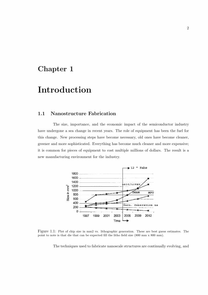
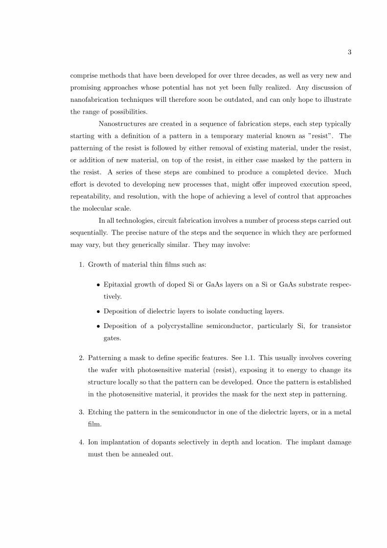
The size, importance, and the economic impact of the semiconductor industry
have undergone a sea change in recent years. The role of equipment has been the fuel for
this change. New processing steps have become necessary, old ones have become cleaner,
greener and more sophisticated. Everything has become much cleaner and more expensive;
it is common for pieces of equipment to cost multiple millions of dollars. The result is a
new manufacturing environment for the industry.
Figure 1.1: Plot of chip size in mm2 vs. lithographic generation. These are best guess estimates. Thepoint to note is that die that can be expected fill the litho field size (800 mm x 800 mm).
The techniques used to fabricate nanoscale structures are continually evolving, and
3
comprise methods that have been developed for over three decades, as well as very new and
promising approaches whose potential has not yet been fully realized. Any discussion of
nanofabrication techniques will therefore soon be outdated, and can only hope to illustrate
the range of possibilities.
Nanostructures are created in a sequence of fabrication steps, each step typically
starting with a definition of a pattern in a temporary material known as ”resist”. The
patterning of the resist is followed by either removal of existing material, under the resist,
or addition of new material, on top of the resist, in either case masked by the pattern in
the resist. A series of these steps are combined to produce a completed device. Much
effort is devoted to developing new processes that, might offer improved execution speed,
repeatability, and resolution, with the hope of achieving a level of control that approaches
the molecular scale.
In all technologies, circuit fabrication involves a number of process steps carried out
sequentially. The precise nature of the steps and the sequence in which they are performed
may vary, but they generically similar. They may involve:
1. Growth of material thin films such as:
• Epitaxial growth of doped Si or GaAs layers on a Si or GaAs substrate respec-
tively.
• Deposition of dielectric layers to isolate conducting layers.
• Deposition of a polycrystalline semiconductor, particularly Si, for transistor
gates.
2. Patterning a mask to define specific features. See 1.1. This usually involves covering
the wafer with photosensitive material (resist), exposing it to energy to change its
structure locally so that the pattern can be developed. Once the pattern is established
in the photosensitive material, it provides the mask for the next step in patterning.
3. Etching the pattern in the semiconductor in one of the dielectric layers, or in a metal
film.
4. Ion implantation of dopants selectively in depth and location. The implant damage
must then be annealed out.
4
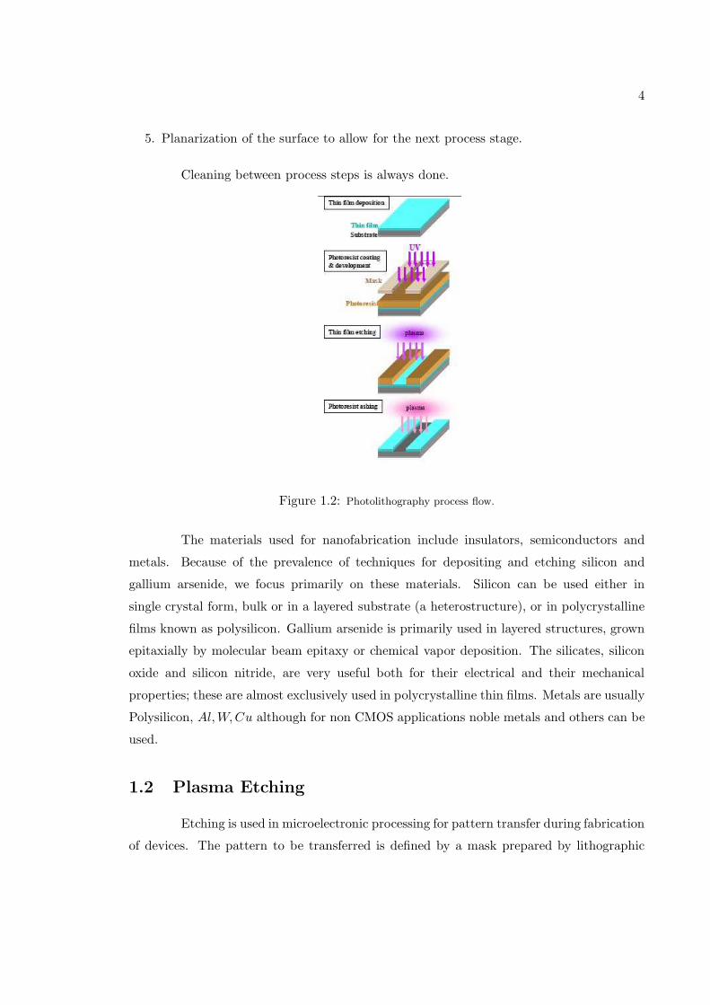
5. Planarization of the surface to allow for the next process stage.
Cleaning between process steps is always done.
Figure 1.2: Photolithography process flow.
The materials used for nanofabrication include insulators, semiconductors and
metals. Because of the prevalence of techniques for depositing and etching silicon and
gallium arsenide, we focus primarily on these materials. Silicon can be used either in
single crystal form, bulk or in a layered substrate (a heterostructure), or in polycrystalline
films known as polysilicon. Gallium arsenide is primarily used in layered structures, grown
epitaxially by molecular beam epitaxy or chemical vapor deposition. The silicates, silicon
oxide and silicon nitride, are very useful both for their electrical and their mechanical
properties; these are almost exclusively used in polycrystalline thin films. Metals are usually
Polysilicon, Al,W,Cu although for non CMOS applications noble metals and others can be
used.
1.2 Plasma Etching
Etching is used in microelectronic processing for pattern transfer during fabrication
of devices. The pattern to be transferred is defined by a mask prepared by lithographic
5
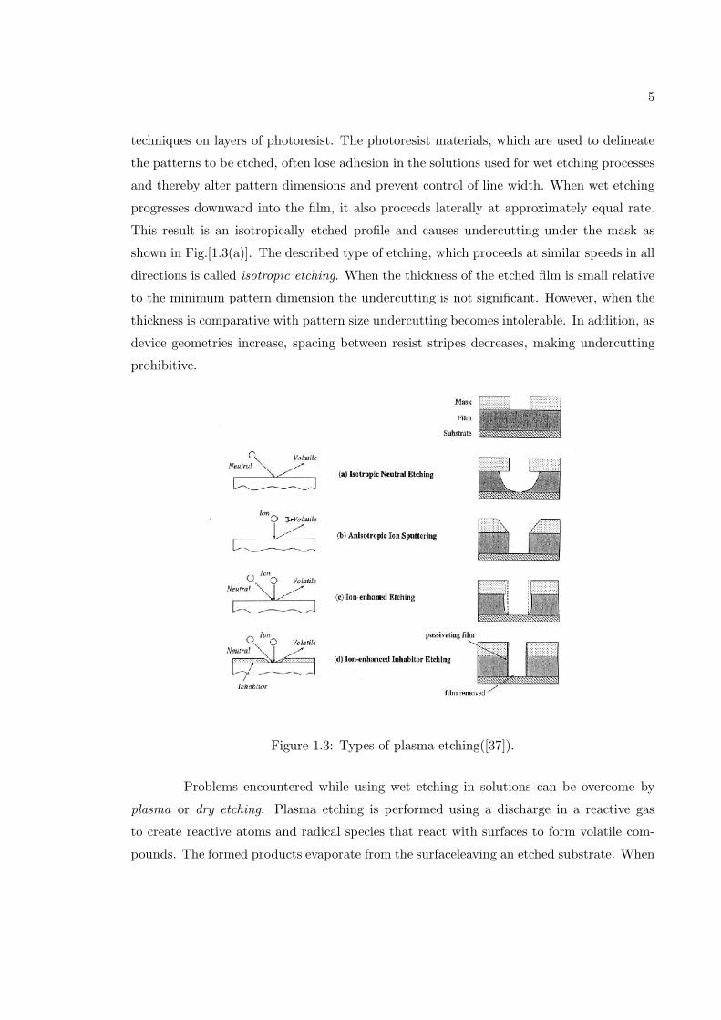
techniques on layers of photoresist. The photoresist materials, which are used to delineate
the patterns to be etched, often lose adhesion in the solutions used for wet etching processes
and thereby alter pattern dimensions and prevent control of line width. When wet etching
progresses downward into the film, it also proceeds laterally at approximately equal rate.
This result is an isotropically etched profile and causes undercutting under the mask as
shown in Fig.[1.3(a)]. The described type of etching, which proceeds at similar speeds in all
directions is called isotropic etching. When the thickness of the etched film is small relative
to the minimum pattern dimension the undercutting is not significant. However, when the
thickness is comparative with pattern size undercutting becomes intolerable. In addition, as
device geometries increase, spacing between resist stripes decreases, making undercutting
prohibitive.
Figure 1.3: Types of plasma etching([37]).
Problems encountered while using wet etching in solutions can be overcome by
plasma or dry etching. Plasma etching is performed using a discharge in a reactive gas
to create reactive atoms and radical species that react with surfaces to form volatile com-
pounds. The formed products evaporate from the surfaceleaving an etched substrate. When
6
using plasma etching, adhesion is no longer a major problem, undercutting can be controlled
by vaying the plasma chemistry and parameters, and directional or anisotropic profiles can
thus be generated. For further reading one can refer to [42].
Etch directionality is required in fabrication of features of high-aspect ratios such as
the deep trenches (> 5µm) used for storage capacitors in silicon wafers. The etching process
is called anisotropic etching when it proceeds much faster in one direction as compared to
other directions. The directionality, or anisotropy, is defined by the ratio of vertical to
horizontal etching rate. The degree of isotropic etching, IE, can be defined by [14]
IE =lude
(1.1)
where lu =amount of undercut at the end of etching and de = thickness of etched
layer.
The degree of anisotropic etching is correspondingly
AE = l − IE. (1.2)
In addition to isotropy/anisotropy, another important etching characteristic is the
etch selectivity. Etch selectivity between to materials is defined as the ratio between their
etching rates at identical plasma conditions. Etch selectivity usually refers to a high etching
rate ratio between chemically different materials or between the etched and the underlying
layer. Etch selectivityis required between etch mask and substrate or between different
substrate materials.
The main reason for the development of the plasma enhanced chemical processing
techniques and expansion of their use over wet chemical etching is the ability to achieve
good control of the process necessary to obtain the required shape of the etched area. An
etching process should satisfy a number of requirements, including:
• High etching selectivity of the layer to be etched with respect to the mask material
and underlying layers.
• Control of the etched profile through control of etching anisotropy.
• High etching rates.
• Uniformity of etching across wafer surfaces.
7
• Minimal material damage.
• Residue-free surface after etching.
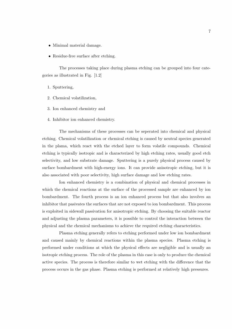
The processes taking place during plasma etching can be grouped into four cate-
gories as illustrated in Fig. [1.2]
1. Sputtering,
2. Chemical volatilization,
3. Ion enhanced chemistry and
4. Inhibitor ion enhanced chemistry.
The mechanisms of these processes can be seperated into chemical and physical
etching. Chemical volatilization or chemical etching is caused by neutral species generated
in the plama, which react with the etched layer to form volatile compounds. Chemical
etching is typically isotropic and is characterized by high etching rates, usually good etch
selectivity, and low substrate damage. Sputtering is a purely physical process caused by
surface bombardment with high-energy ions. It can provide anisotropic etching, but it is
also associated with poor selectivity, high surface damage and low etching rates.
Ion enhanced chemistry is a combination of physical and chemical processes in
which the chemical reactions at the surface of the processed sample are enhanced by ion
bombardment. The fourth process is an ion enhanced process but that also involves an
inhibitor that pasivates the surfaces that are not exposed to ion bombardment. This process
is exploited in sidewall passivation for anisotropic etching. By choosing the suitable reactor
and adjusting the plasma parameters, it is possible to control the interaction between the
physical and the chemical mechanisms to achieve the required etching characteristics.
Plasma etching generally refers to etching performed under low ion bombardment
and caused mainly by chemical reactions within the plasma species. Plasma etching is
performed under conditions at which the physical effects are negligible and is usually an
isotropic etching process. The role of the plasma in this case is only to produce the chemical
active species. The process is therefore similar to wet etching with the difference that the
process occurs in the gas phase. Plasma etching is performed at relatively high pressures.

8
(a) Spontaneous surface etching reactions. (b) Chemical sputtering during etching.
(c) Ion-enhanced etching process.
Figure 1.4: Mechanisms of surface etching([10]).
9
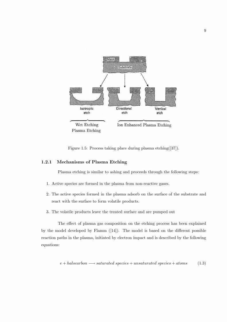
Figure 1.5: Process taking place during plasma etching([37]).
1.2.1 Mechanisms of Plasma Etching
Plasma etching is similar to ashing and proceeds through the following steps:
1. Active species are formed in the plasma from non-reactive gases.
2. The active species formed in the plasma adsorb on the surface of the substrate and
react with the surface to form volatile products.
3. The volatile products leave the treated surface and are pumped out
The effect of plasma gas composition on the etching process has been explained
by the model developed by Flamm ([14]). The model is based on the different possible
reaction paths in the plasma, initiated by electron impact and is described by the following
equations:
e + halocarbon −→ saturated species + unsaturated species + atoms (1.3)

10
reactive atoms/molecules + unsatured species −→ saturated species (1.4)
atoms + surface −→ chemisorbed layer + volatile products (1.5)
unsaturated species + surfaces −→ films (1.6)
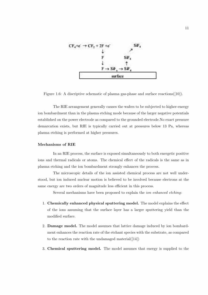
The corresponding reactions in a CF4 plasma are
2e + 2CF4 −→ CF3 + CF2 + 3F + 2e (1.7)
F + CF2 −→ CF3 (1.8)
4F + CF2 −→ SiF4 (1.9)
nCF2 + surface −→ (CF2)n (1.10)
According to this model, the final result of the interaction between a CF4 plasma
and silicon depends on the generated species. If the main path in the plasma reactions
follows Eq. (1.9), the result will be etching; if the main path in the plasma reactions is
described by Eq. (1.8), the result will be recombination; if the main path in the plasma
reactions is described by Eq. (1.10), the result will be film formation (polymerization).
Gas-phase oxidant additives (O2, F2 etc.) can dissociate and react with unsaturated species,
changing the relative concentration of the species and the reaction paths.
1.2.2 Reactive Ion Etching
Reactive ion etching is the most used by dry etching technique. RIE is based on a
combination of chemical activity of reactive species generated in the plasma with physical
effects caused by ion bombardment. When substrates to be etched are positioned on the
powered electrode of a parallel plate reactor, as illustrated in Fig. ??, a reactive ion etching
or reactive sputter etching configuration results. a negative DC bias is generated on the
sample electrode, usually by applying RF power to electrode.
11
Figure 1.6: A discriptive schematic of plasma gas-phase and surface reactions([10]).
The RIE arrangement generally causes the wafers to be subjected to higher-energy
ion bombardment than in the plasma etching mode because of the larger negative potentials
established on the power electrode as compared to the grounded electrode.No exact pressure
demarcation exists, but RIE is typically carried out at pressures below 13 Pa, whereas
plasma etching is performed at higher pressures.
Mechanisms of RIE
In an RIE process, the surface is exposed simultaneously to both energetic positive
ions and thermal radicals or atoms. The chemical effect of the radicals is the same as in
plasma etching and the ion bombardment strongly enhances the process.
The microscopic details of the ion assisted chemical process are not well under-
stood, but ion induced nuclear motion is believed to be involved because electrons at the
same energy are two orders of magnitude less efficient in this process.
Several mechanisms have been proposed to explain the ion enhanced etching :
1. Chemically enhanced physical sputtering model. The model explains the effect
of the ions assuming that the surface layer has a larger sputtering yield than the
modified surface.
2. Damage model. The model assumes that lattice damage induced by ion bombard-
ment enhances the reaction rate of the etchant species with the substrate, as compared
to the reaction rate with the undamaged material([14])
3. Chemical sputtering model. The model assumes that energy is supplied to the
12
reaction layer by the collision cascades induced by ion bobmbardment; this energy
increases the mobility of molecules which form volatile products and desorb from the
surface.
According to these models, both the reaction step and the removal of the valatile
reaction products formed on the etched surface are enhanced by ion bombardment. The
predominance of one mechanism over the other is determined in each case by the etchant-
substrate combination.
Selectivity
Etch selectivity is caused by the different rates of the processes taking place on the
different materials. These processes include adsorption of etching species and desorption of
the volatile etching product.
Etch selectivity can also be achieved according to the damage model described ear-
lier. Ion bombardment generally impacts different degrees of damage to various materials.
By changing the energy of the bombarding ions, etching selectivity can be altered to tailor
a specific etching process. Nevertheless, etch selectivity is more difficult to achieve in RIE
than in wet chemical etching, because the ion bombardment makes the chemical difference
between materials less important.
The bombardement of the substrate with the high-energy ions can induce damage
to the surface layers of the etched wafer. The damaged layer and the fluorocarbon film
deposited on the Si surface have to be removed before further processing the wafer.
The etching rates are generally low in RIE, and many wafers have to be processed
simultaneously to obtain reasonable commercial throughputs. The transition to processing
of larger silicon wafers requires single-wafer processing and faster etching-rates. Directional
faster etching rates were obtained using ECR or magnetically enhanced reactive ion etcher
reactors. While etching in RIE is obtained from a small flux of high-energy ions, large fluxes
of low-energy ions characterize the ECR and MERIE processes.
1.3 Roughness in thin film technologies
Interface roughness is one of the key features in many important thin film technolo-
gies. The roughness of the interface directly controls many physical and chemical properties
13
of the film. For example, the increase of the contact angle of a small liquid droplet on a
rough surface compared to that on a smooth surface [15], shifts of Brewster angle on a
rough surfaces [53, 17], roughness dependent demagnetizing fields and coercivity of thin
magnetic films [55, 43] , and roughness dependent electrical conductivity of thin metal films
[16]. The roughness also affects surface plasmon [13], surface second harmonic generation
[40, 30], and the chemical reaction rate [1].
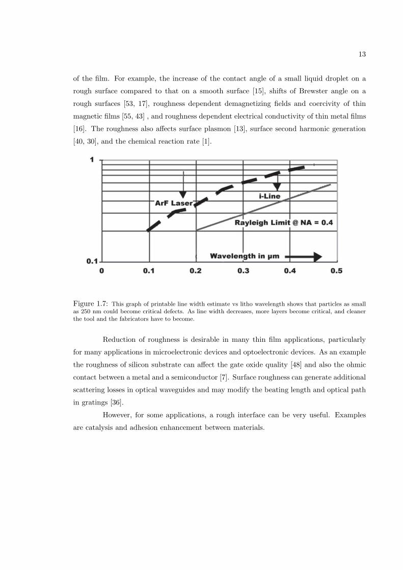
Figure 1.7: This graph of printable line width estimate vs litho wavelength shows that particles as smallas 250 nm could become critical defects. As line width decreases, more layers become critical, and cleanerthe tool and the fabricators have to become.
Reduction of roughness is desirable in many thin film applications, particularly
for many applications in microelectronic devices and optoelectronic devices. As an example
the roughness of silicon substrate can affect the gate oxide quality [48] and also the ohmic
contact between a metal and a semiconductor [7]. Surface roughness can generate additional
scattering losses in optical waveguides and may modify the beating length and optical path
in gratings [36].
However, for some applications, a rough interface can be very useful. Examples
are catalysis and adhesion enhancement between materials.

14
Chapter 2
Roughness Characterizations
Rough surfaces can be found everywhere, and are the research objects in many
fields including tribology, geophysics, remote sensoring, acoustics, etc.
Before proceeding, it is necessary to define precisely what is meant by the term
surface roughness. A surface can be regarded as the boundary of a connected two dimen-
sional space. We will assume that the surface can be described by a height function h(x).
The surface will then be the boundary where y < h(x).
2.0.1 Types of rough surfaces
Before introducing quantitative parameters for describing rough surfaces , it is first
necessary to introduce the general classes of rough surfaces. First, any surface that deviates
from being perfectly flat will be be called rough. There are two different kinds of rough
surfaces of particular interest: mounded surfaces and self-affine surfaces. Two examples of
real rough surfaces can be seen in figures 2.0.1,2.0.1.
Self-Affine and Self Similar surfaces
An approach to the understanding of surface evolution employs the concept of
topographical scaling . The most familiar type of scaling is self-similarity , which is a
restricted case of a more general class, self affinity. A surface h(x) is said to be self-similar
if kh(kx) is indistinguishable from h(x),but if the y-axis must be multiplied by a different
factor, i.e. kh(bx), then h is self-affine.
Many real surfaces appear to be self-affine over a restricted range of length scales

15
Figure 2.1: Example of a rough surface and its 2d projection produced by a linescan as the result of anthe etching of a silicon wafer in SF6 plasma.
(32, 35, 36),and this observation has stimulated the application of fractal geometry to the
study of surface growth (37-39).
The patterns that form during the growth of surfaces are similar for very different
materials and over many orders of magnitude in film thickness for the case of deposition.
Different communities of researchers have discovered the fractal-like nature of these patterns
and have developed quantitative means for analyzing the structure and understanding the
origins of the patterns, often in complete isolation from one another.
Mounded Surfaces
A mounded surface needn’t actually be composed of mounds; a surface consisting
of regularly spaced holes could also be called mounded. The key element that characterizes
a mounded surface is the existance of a geometric structure acting as a building element
that gets repeated over the entire profile with a characteristic spacing ζ. The arrangement
of mounds isn’t perfectly periodic. Furthermore the mounds needn’t be identical to each
other. An example of a mounded surface can be seen in 2.0.1.
Dual Surfaces
A third class of surfaces than can be introduced is those having a dual morphology.
These surfaces exhibit both the characteristics of a mounded surface and of a self affine

16
Figure 2.2: Example of a mounded surface.Note the characteristic spacing unit ζ.
surface. They have large mounds but at the same time needle-like topologies stick out
everywhere breaking down the mound symmetry. Their height distribution is usually very
skewed showing a large tail of big heights, the needles, whereas they also have a distinct
periodic component of larger wavelength, the pits. For an example of such a surface see
figure 2.0.1.
Figure 2.3: Example of a rough surface with dual morphology produced by the etching of a silicon waferin SF6 plasma.
2.1 Roughness Parameters
Once it is known what class a surface belongs to, there still remains the task of
finding a suitable quantitative description to the surface. This can be accomplished by
using an appropriate set of roughness parameters. Which set of parameters is appropriate

17
will, in general, depend on the specific class to which the surface belongs.
2.1.1 Surface Statistical Functions
Before introducing the roughness parameters, it is helpfull to first introduce the
various statistical functions that we will use to describe rough surfaces.
The first function is the Height-Height correlation function H(x) which is defined
as :
H(x) =⟨
[h(x0 + x) − h(x)]2⟩
(2.1)
Note that the braces denote a statistical average over all x0.
Another usefull function that is used is the autocorrelation function, defined by
G(x) =⟨[
h(x0 + x) − h] [
h(x0) − h]⟩
(2.2)
The power spectrum density is defined as:
P (k) =∣
∣
∣
⟨
[
h(x0) − h]
eik·x0
⟩∣
∣
∣
2(2.3)
2.1.2 Scaling of the Interface Width for Self Affine and Self Similar Sur-
faces
In 1985, Family and Vicsek ,[12] ,analyzed the behavior of growing surfaces by
assuming that they were self-affine. They showed that the standard deviation of the surface
height w, also called the interface width, of a growing self-affine surface can be expressed
in the form (2.4)
w(L, t) = Laf(t/Lz) (2.4)
where f(x) is a function that behaves as a for x << 1 and as a constant for x >> 1.
This reduces to w(L, t) ∝ tβ for t/Lz << l and to w(L, t) ∝ La for t/Lz >> 1 where
L is the length scale over which the roughness is measured and t is the elapsed time of
growth (or etching), which is usually proportional to the amount of material deposited (or
removed). The two new parameters α and β are called the static (or spatial) and dynamic
(or temporal) scaling exponents, respectively, and z isα
β.
As illustrated in Figure 2.4 the rms roughness of a surface is actually a function of
the length scale L over which it is measured until the roughness saturates at some critical
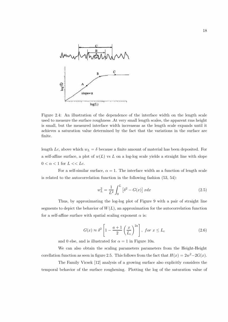
18
Figure 2.4: An illustration of the dependence of the interface width on the length scaleused to measure the surface roughness .At very small length scales, the apparent rms heightis small, but the measured interface width increaseas as the length scale expands until itachieves a saturation value determined by the fact that the variations in the surface arefinite.
length Lc, above which wL = δ because a finite amount of material has been deposited. For
a self-affine surface, a plot of w(L) vs L on a log-log scale yields a straight line with slope
0 < α < 1 for L << Lc.
For a self-similar surface, α = 1. The interface width as a function of length scale
is related to the autocorrelation function in the following fashion (53, 54):
w2L =
1
L2
∫ L
0
[
δ2 − G(x)]
xdx (2.5)
Thus, by approximating the log-log plot of Figure 9 with a pair of straight line
segments to depict the behavior of W (L), an approximation for the autocorrelation function
for a self-affine surface with spatial scaling exponent α is:
G(x) ≈ δ2
[
1 − a + 1
2
(
x
Lc
)2a]
, for x ≤ Lc (2.6)
and 0 else, and is illustrated for α = 1 in Figure 10a.
We can also obtain the scaling parameters parameters from the Height-Height
corellation function as seen in figure 2.5. This follows from the fact that H(x) = 2w2−2G(x).
The Family Vicsek [12] analysis of a growing surface also explicitly considers the
temporal behavior of the surface roughening. Plotting the log of the saturation value of
19
Figure 2.5: A log-log plot of the surface height-height correlation function for a self affinesurface. The interface width w , the correlation length ξ , and the roughness exponent αare indicated by the dashed lines [9]
w(L) vs log(t) yields a straight line with a slope of β for a growing self-affine surface (inset
of 2.6). Thus, the time dependence of the surface rms is determined from equation δ ∝ tβ
if β is known. Moreover, because the critical length for scaling and the deposition time are
related to each other by t/Lzc ∝ 1 , the time dependence of the lateral correlation length is
also known to be ξ ∝ β/α. Figure 2.6 shows how the temporal dependence of δ and ξ can
be determined from the spatial and temporal dependence of W (L).
If the growing surface is self-similar (α = 1) at any time, then the correlation
length and the surface rms have the same time dependence, and thus the surface will be
self-similar at all times. However if the surface is self-affine, then the correlation length of
the surface must increase faster than the surface rms, and thus the ratio δ/ξ will decrease
with time. The amplitude of the rms of a self-affine surface will increase, but the corrugation
will decrease as the surface is being etched.
The parameters α and β provide a pair of numbers that can be used to classify
the spatial and temporal scaling of growing surfaces quantitatively, and thereby identify
the etching process according to its symmetry in a renormalization group sense. If the two
system-dependent parameters δ and Lc are also known at some time z, the surface rms and

20
Figure 2.6: A log log plot of the saturation value ξ versus the surface dimension
the correlation length can be predicted for all times during the growth of the surface:
δ(t) = δ(τ)
(
t
τ
)β
and Lc(t) = Lc(τ)
(
t
τ
)β
(2.7)
Thus, if growing surfaces are truly self-affine, they can, in principle, be completely charac-
terized in space and time by only five numbers: The scaling exponents should be universal
and predictable from theory,whereas the surface rms and correlation length are system de-
pendent and must be measured at least once for each particular set of growth conditions.
In some cases predicted by theory , additional constraints relate α and β, so that in fact
the entire spatial and temporal evolution of a growing surface may be determined from only
four independent parameters, which reveals a remarkable simplicity underlying the complex
process of surface etching.
2.1.3 Anomalous roughening
It is quite easily understood that the Family-Viscek scaling theory is not the most
general for a surface displaying kinetic roughening. Thus, it might be the case that, at
least in some systems , the values attributed to the scaling exponents were not correct but,
rather, originated in trying to t the data using the wrong scaling theory. This type of scaling
21
has been termed anomalous. At least in many cases studied, it originates in slow dynamics
of the surface slopes, which do not reach a stationary state simultaneously with the surface
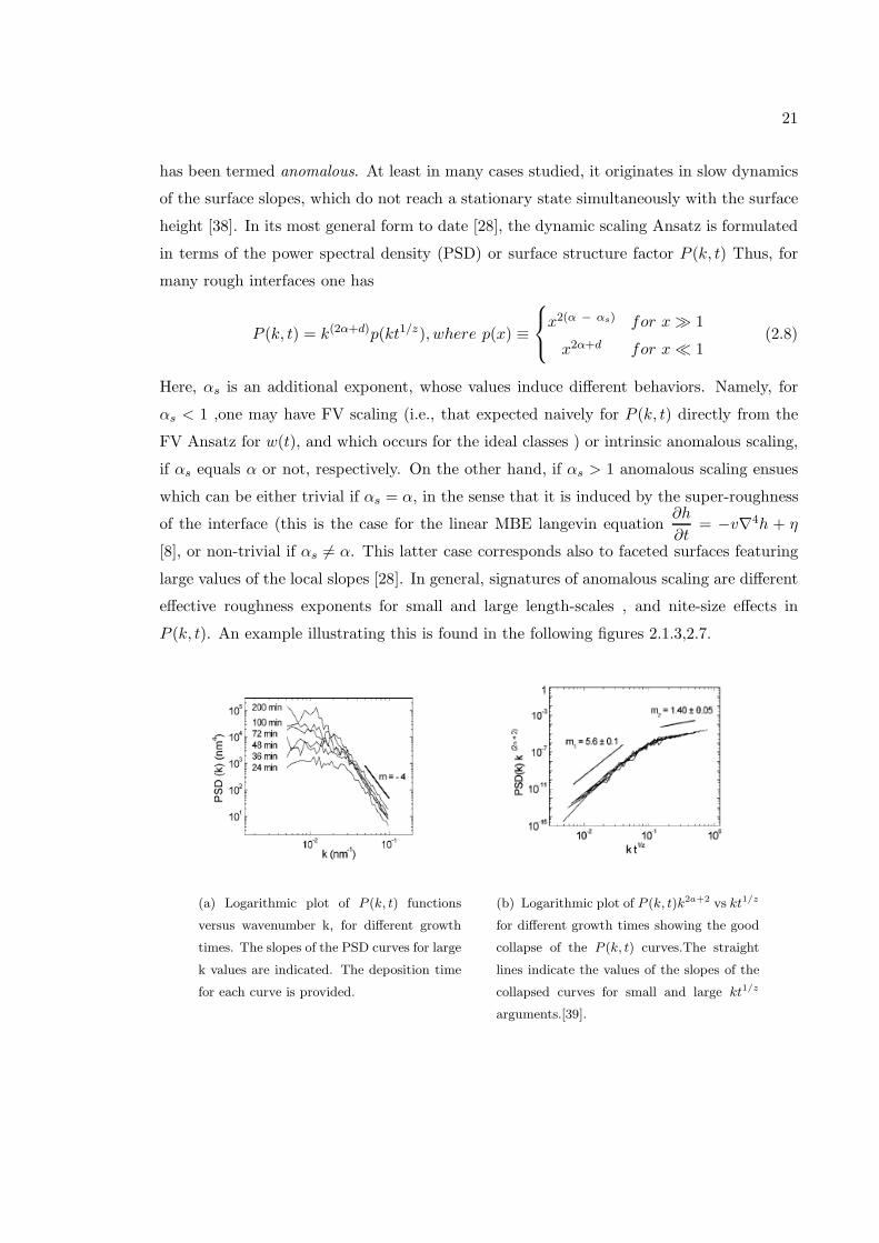
height [38]. In its most general form to date [28], the dynamic scaling Ansatz is formulated
in terms of the power spectral density (PSD) or surface structure factor P (k, t) Thus, for
many rough interfaces one has
P (k, t) = k(2α+d)p(kt1/z), where p(x) ≡
x2(α − αs) for x ≫ 1
x2α+d for x ≪ 1(2.8)
Here, αs is an additional exponent, whose values induce different behaviors. Namely, for
αs < 1 ,one may have FV scaling (i.e., that expected naively for P (k, t) directly from the
FV Ansatz for w(t), and which occurs for the ideal classes ) or intrinsic anomalous scaling,
if αs equals α or not, respectively. On the other hand, if αs > 1 anomalous scaling ensues
which can be either trivial if αs = α, in the sense that it is induced by the super-roughness
of the interface (this is the case for the linear MBE langevin equation∂h
∂t= −v∇4h + η
[8], or non-trivial if αs 6= α. This latter case corresponds also to faceted surfaces featuring
large values of the local slopes [28]. In general, signatures of anomalous scaling are different
effective roughness exponents for small and large length-scales , and nite-size effects in
P (k, t). An example illustrating this is found in the following figures 2.1.3,2.7.
(a) Logarithmic plot of P (k, t) functions
versus wavenumber k, for different growth
times. The slopes of the PSD curves for large
k values are indicated. The deposition time
for each curve is provided.
(b) Logarithmic plot of P (k, t)k2a+2 vs kt1/z
for different growth times showing the good
collapse of the P (k, t) curves.The straight
lines indicate the values of the slopes of the
collapsed curves for small and large kt1/z
arguments.[39].

22
Figure 2.7: Power spectral density behaviour vs exposure time. The times are from theuppermost curve in descending order:600s,240s,120s,30s,[47]
Note that as time evolves small length-scales play a crucial role in the roughening.
For another example and more details see either [8] section 3,[29].
To date, there is no general argument as to what kind of scaling eld controls the
value of the exponent αs in those cases in which it is actually independent from α, z and
geometrical constants. In some examples such as interfaces generated in invasion percolation
models, the value of αs can be related with the fractal properties of the underlying cluster.
This may provide a physical interpretation for the anomalous scaling properties. Since
inhibiting species contaminating the wafer resemble invasion percolation models in a way,
we will therefore try to prove that the plasma reaction’s condition and contamination leads
to anomalous roughness scaling in the wafer.
2.1.4 Scaling of the Interface Width for Mounded Surfaces
The scaling relations presented above will not hold for mounded surfaces. One can
still obtain values for w and ξ as in the self affine case, but if one attempts to find a value
for the α this value will usually be close to unity, noting the fact that these surfaces have
a strong generic periodicity . It is much more convenient to use the power spectral density
for these surfaces. Note, this implies that all three statistical functions described in 2.1.1
ultimately contain the same information.
23
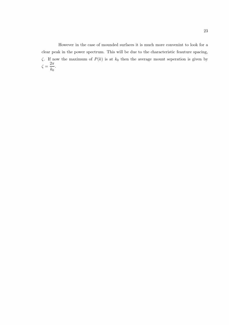
However in the case of mounded surfaces it is much more convenint to look for a
clear peak in the power spectrum. This will be due to the characteristic feauture spacing,
ζ. If now the maximum of P (k) is at k0 then the average mount seperation is given by
ζ =2π
k0.
24
Chapter 3
Previous Work
The subject of kinetic roughening and non-equilibrium growths, have been in the
center of interest of far-from equilibrium physics for more than two decades now. Although
the processes which have been probed so far, have mostly been concerned only with local
effects, such as molecular-beam epitaxy (MBE) growth, conventional diffusive growths, etc,
the importance of the non-local effects, have been known as early as the 1950s [32]. Whereas
in standard MBE type of growths, the vapor atoms are targetted in a direction normal to
the substrate, so that growth is decided by the local environment only, in case of shadowing
growths by sputter deposition, vapor atoms are incident at random angles to the surface,
so that non-local factors gain prominence in this case [32, 46, 45, 2, 58]. There have been
several experimental follow-ups too of this sputtering mechanism [20, 62].
There are 2 main simulation techniques used in literature. Continuum modelling
of the surface using PDE’s or Discrete representations of the surface and change of the
according to a monte carlo procedure.
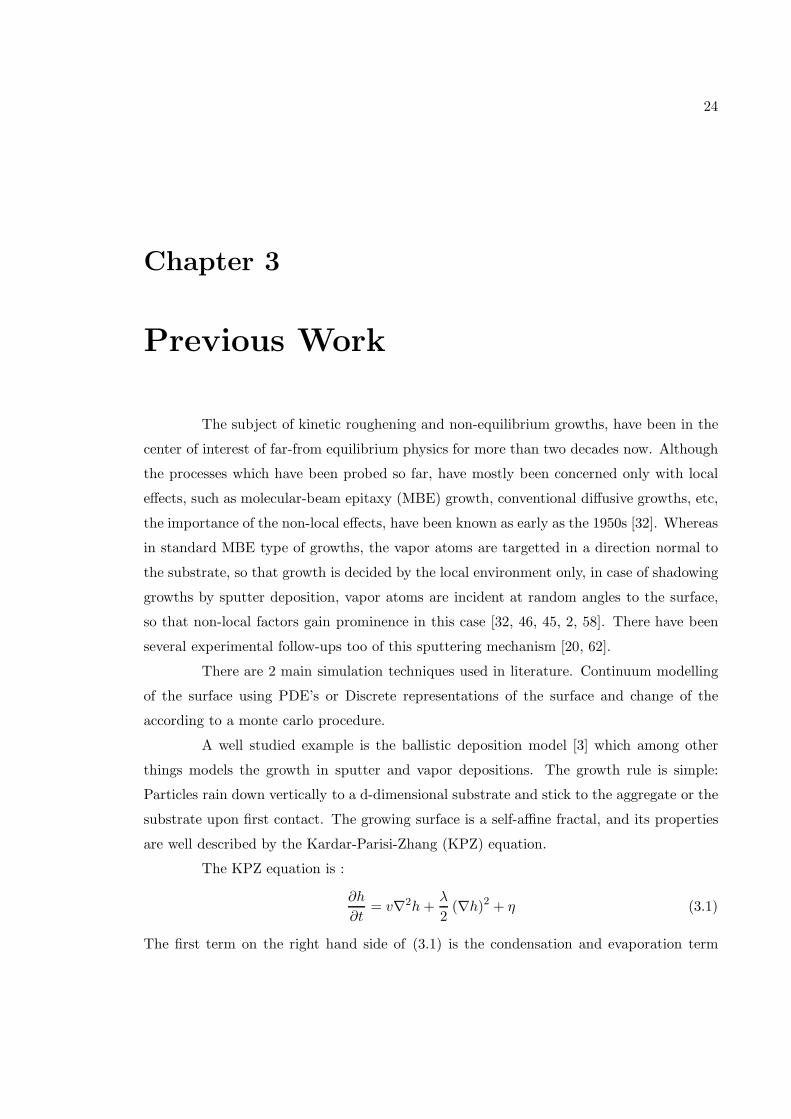
A well studied example is the ballistic deposition model [3] which among other
things models the growth in sputter and vapor depositions. The growth rule is simple:
Particles rain down vertically to a d-dimensional substrate and stick to the aggregate or the
substrate upon first contact. The growing surface is a self-affine fractal, and its properties
are well described by the Kardar-Parisi-Zhang (KPZ) equation.
The KPZ equation is :
∂h
∂t= v∇2h +
λ
2(∇h)2 + η (3.1)
The first term on the right hand side of (3.1) is the condensation and evaporation term
25
whereas the second grows the surface proportionally to the local curvature.The third term
is quenched noise.
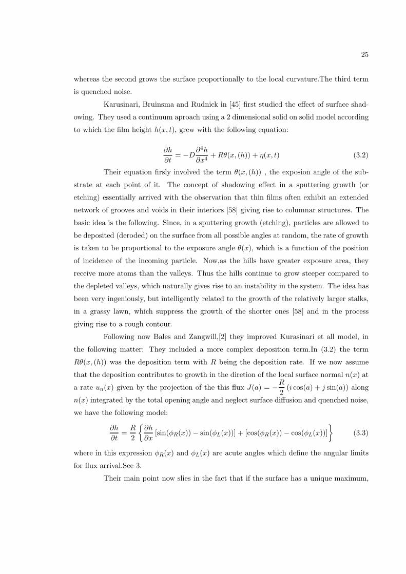
Karusinari, Bruinsma and Rudnick in [45] first studied the effect of surface shad-
owing. They used a continuum aproach using a 2 dimensional solid on solid model according
to which the film height h(x, t), grew with the following equation:
∂h
∂t= −D
∂4h
∂x4+ Rθ(x, (h)) + η(x, t) (3.2)
Their equation firsly involved the term θ(x, (h)) , the exposion angle of the sub-
strate at each point of it. The concept of shadowing effect in a sputtering growth (or
etching) essentially arrived with the observation that thin films often exhibit an extended
network of grooves and voids in their interiors [58] giving rise to columnar structures. The
basic idea is the following. Since, in a sputtering growth (etching), particles are allowed to
be deposited (deroded) on the surface from all possible angles at random, the rate of growth
is taken to be proportional to the exposure angle θ(x), which is a function of the position
of incidence of the incoming particle. Now,as the hills have greater exposure area, they
receive more atoms than the valleys. Thus the hills continue to grow steeper compared to
the depleted valleys, which naturally gives rise to an instability in the system. The idea has
been very ingeniously, but intelligently related to the growth of the relatively larger stalks,
in a grassy lawn, which suppress the growth of the shorter ones [58] and in the process
giving rise to a rough contour.
Following now Bales and Zangwill,[2] they improved Kurasinari et all model, in
the following matter: They included a more complex deposition term.In (3.2) the term
Rθ(x, (h)) was the deposition term with R being the deposition rate. If we now assume
that the deposition contributes to growth in the diretion of the local surface normal n(x) at
a rate un(x) given by the projection of the this flux J(a) = −R
2(i cos(a) + j sin(a)) along
n(x) integrated by the total opening angle and neglect surface diffusion and quenched noise,
we have the following model:
∂h
∂t=
R
2
∂h
∂x[sin(φR(x)) − sin(φL(x))] + [cos(φR(x)) − cos(φL(x))]
(3.3)
where in this expression φR(x) and φL(x) are acute angles which define the angular limits
for flux arrival.See 3.
Their main point now slies in the fact that if the surface has a unique maximum,

26
this will advance with respect to the Huygen’s principle and spread out like an optical wave
front,possibly explaining microstructures observed in many cases of thin film growth.
Roland and Guo, [52] ,where the first to explore the shadowing effect using a monte
carlo approach. Again, they used the SOS (Solid On Solid) approximation to exclude over-
hangs. They used a kinetic lattice monte carlo approach since they follow the trajectories
of the particles inside a square lattice. They were the first to calculate the parameter ζ(t).
There control parametes for the SOS Hamiltonian also included the Temperature T and
θmax, an angle ,whith which the particles were not allowed to surpass when they started
their ballistic trajectory above the substrate. This angle measured the relative importance
of the shadowing effect.They also further predicted that in the low temperature phase, the
system resembles a KPZ universality class . Finally in [21], they exploited the properties
of a three dimensional continuum model for shadowing growth that was
∂h
∂t= v∇2h + RΩ(r, h) + η (3.4)
where the second term on the right hand side is the three dimensinal analogue to (3.2).
Krug and Meakin, [33] used a simple SOS grass model for sputter deposition, as
an extension to [46] in order to exploit the long time coarsening dynamics of the columnar
microstructure. They modelled the surface as being a discrete set of columns each with a
different height. The dynamics that governed the growth rate of each column was given by:
dhi
dt= V (θi) (3.5)
where V is a monotonically increasing function of the angle with V(0)=0. They agree with
[52] in their coarsening exponent but their model did not incorporate any noise, rather than
an assumption for the distribution of the heights of the initial surface.
Tang and Liang, [59] used also a 2 dimensional kinetic monte carlo method with
a triangular grid . They studied the ballistic deposition model in which incoming particles

27
come from a range of random angles. They have found two distinct morphological regimes
with respect to a possible bifuraction of the dynamics of the model when the angle grows
bigger than a given angle. For small angles the dynamics are KPZ dominated, whereas for
larger angles the morphology is characterized by stable wedges.
Ko and Seno, [31] tried by using multi-dimensional Monte Carlo simulations on a
square lattice to exploit the possible importance of overhangs in the scaling of the deposition
growth process. They actually found that the presence of overhangs is an important factor
in determining the scaling properties of deposition growth, since when overhangs form , the
surface no longer grows on the direction of its gradient, but rather grows anisotropically.
Later on, the domain of 2+1 dimension was also probed with the advent of ad-
vanced numerical integration algorithms and Monte-Carlo simulations [58, 22, 23]. These
were the works of Jason Drotar [9] with the group of G.C. Wang. They used both a con-
tinuum approach as well as a 3 dimensional kinetic monte carlo on a cubic lattice. The
equation they used to model the shadowing growth-etching is the following:
∂h
∂t= v∇2h − k∇4h ±
√
1 + (∇h)2η (3.6)
The factor√
1 + (∇h)2 is present because the growth and etching are normal to
the local surface.
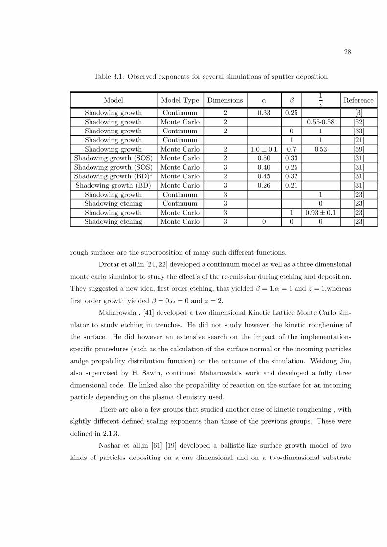
To sum up, all the important information regarding the shadowing growth and
etching simulations are given in the following table:
Another important class of simulations were the ones that included re-emission
effects .
Dew et all, presented in [57] a monte carlo sumulation a ballistic deposition model
including re-emission effects (SIMBAD). They used a string algorithm to evolve the surface
. In addition, they studied the effect of the sticking coefficients on the sidewall coverage of
deep trenches , and also succesfully linked the incident angular distribution function with
the columnar microstructure morphology .
Singh and Shaqfeh [34], used a continuum approach ,solving a complex integral
equation containing the re-emitted flux from all the surface on any possble point of it.
They also studied the effect of the sticking coefficient to the actuall evolution of the surface.
Finally , they provides an insight of the evolution of rough surfaces under LPCVD, by
examining the evolution of sinusoidal funtions with different wavenumbers and stating that
28
Table 3.1: Observed exponents for several simulations of sputter deposition
Model Model Type Dimensions α β1
zReference
Shadowing growth Continuum 2 0.33 0.25 [3]
Shadowing growth Monte Carlo 2 0.55-0.58 [52]
Shadowing growth Continuum 2 0 1 [33]
Shadowing growth Continuum 1 1 [21]
Shadowing growth Monte Carlo 2 1.0 ± 0.1 0.7 0.53 [59]
Shadowing growth (SOS) Monte Carlo 2 0.50 0.33 [31]
Shadowing growth (SOS) Monte Carlo 3 0.40 0.25 [31]
Shadowing growth (BD)1 Monte Carlo 2 0.45 0.32 [31]
Shadowing growth (BD) Monte Carlo 3 0.26 0.21 [31]
Shadowing growth Continuum 3 1 [23]
Shadowing etching Continuum 3 0 [23]
Shadowing growth Monte Carlo 3 1 0.93 ± 0.1 [23]
Shadowing etching Monte Carlo 3 0 0 0 [23]
rough surfaces are the superposition of many such different functions.
Drotar et all,in [24, 22] developed a continuum model as well as a three dimensional
monte carlo simulator to study the effect’s of the re-emission during etching and deposition.
They suggested a new idea, first order etching, that yielded β = 1,α = 1 and z = 1,whereas
first order growth yielded β = 0,α = 0 and z = 2.
Maharowala , [41] developed a two dimensional Kinetic Lattice Monte Carlo sim-
ulator to study etching in trenches. He did not study however the kinetic roughening of
the surface. He did however an extensive search on the impact of the implementation-
specific procedures (such as the calculation of the surface normal or the incoming particles
andge propability distribution function) on the outcome of the simulation. Weidong Jin,
also supervised by H. Sawin, continued Maharowala’s work and developed a fully three
dimensional code. He linked also the propability of reaction on the surface for an incoming
particle depending on the plasma chemistry used.
There are also a few groups that studied another case of kinetic roughening , with
slghtly different defined scaling exponents than those of the previous groups. These were
defined in 2.1.3.
Nashar et all,in [61] [19] developed a ballistic-like surface growth model of two
kinds of particles depositing on a one dimensional and on a two-dimensional substrate
29
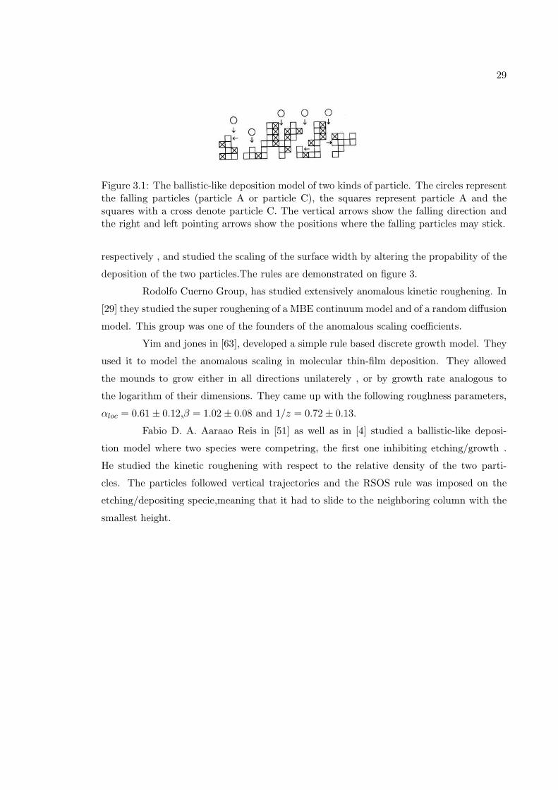
Figure 3.1: The ballistic-like deposition model of two kinds of particle. The circles representthe falling particles (particle A or particle C), the squares represent particle A and thesquares with a cross denote particle C. The vertical arrows show the falling direction andthe right and left pointing arrows show the positions where the falling particles may stick.
respectively , and studied the scaling of the surface width by altering the propability of the
deposition of the two particles.The rules are demonstrated on figure 3.
Rodolfo Cuerno Group, has studied extensively anomalous kinetic roughening. In
[29] they studied the super roughening of a MBE continuum model and of a random diffusion
model. This group was one of the founders of the anomalous scaling coefficients.
Yim and jones in [63], developed a simple rule based discrete growth model. They
used it to model the anomalous scaling in molecular thin-film deposition. They allowed
the mounds to grow either in all directions unilaterely , or by growth rate analogous to
the logarithm of their dimensions. They came up with the following roughness parameters,
αloc = 0.61 ± 0.12,β = 1.02 ± 0.08 and 1/z = 0.72 ± 0.13.
Fabio D. A. Aaraao Reis in [51] as well as in [4] studied a ballistic-like deposi-
tion model where two species were competring, the first one inhibiting etching/growth .
He studied the kinetic roughening with respect to the relative density of the two parti-
cles. The particles followed vertical trajectories and the RSOS rule was imposed on the
etching/depositing specie,meaning that it had to slide to the neighboring column with the
smallest height.
30
3.1 Thesis Goals
The goals of this thesis are:
1. To simulate , model and evaluate various roughnening mechanisms.
2. To categorize and characterize various rough profiles .
3. To find scaling laws differentiating between the various roughening processes.
4. To find limiting behaviour of some of the roughness parameters.
5. To establish plasma etching in a contaminated reactor as an anomalous-roughening
inducing procedure.
To be more precise, we will use a kinetic lattice monte carlo approach in order
to evaluate the shadowing effect in an etching process, and also try to investigate Drotar’s
et all re-emission dominated etching approach. We will try to explain and quantify our
experimental results, showing a linear dependance of roughness to time , (and thus a β = 1)
by using a new approach based on the simultaneous existence of inhibiting and etching
precursors.
We will also use the fractal analysis of surfaces to characterize the outcome of our
simulation’s and compare our results with previous works as long as with our experimental
work.
31
Part II
Monte Carlo Simulation

32
3.2 Description of the the simulation method
The method we have implemented in this thesis is Kinetic Lattice Monte
Carlo .
• Kinetic because we follow the trajectories of particles until they either interact with
the substrate or bounce off back to the plasma bulk.
• Lattice because we discretized the simulation domain using a square lattice. In
order to calibrate our results we will perform the following calculations based on
experimental results:
Etch Rate =Etched Depth
T ime Elapsed(3.7)
Etch Rate =Mlayers · layer width
Ncycles · T ime step=
Mlayers · xNcycles · y
(3.8)
In order to simplify our calculations somewhat, let x be measured in µm and y in min-
utes (min). The numbers M,N are calculated every time we perform our simulation.
However we still need a second equation to solve for our unknown quantities.
Particle F lux =Number of incident particles
Area · Unit T ime step(3.9)
Our surface however is a 1-d line in the plane . Bearing this in mind we will try to
correlate the flux received by a line in the plane with the flux received by a 2-d area.
The silicon lattice consists of many sites, which are however due to the nature of the
crystallic lattice discrete. We assume that they have the following form:
· · ·· · ·· · ·
(3.10)
Each horizontal line consists of M active lattice sites. Therefore, due to the square
natute of the lattice , the whole are consists of M2 sites. This yields the following
argument:

33
Particle F lux2d =Number of particles
cm2 · sec ⇔ Particle F lux1d =
√Number of particles
cm · sec(3.11)
So if we use the above defined quantities ,we arrive in the following relations between
the simulation time unit and the experimental:
SimulationT imeUnit = 0.08seconds (3.12)
LatticepixelUnit = 0.27nanometers (3.13)
Note that the distance of two Silicon atoms in the silicon crystal is measured approx-
imately at 0.255nm. This comes in very good agreements with our simulation since
each square pixel represents in the x direction a silicon atom.
• Monte-Carlo because every trajectory and every interaction is decided upon a ran-
dom toss of a coin. More specifically, (a) the particles are considered to strike the
surface randomly,both in nature and orientation, (b) the process that describes the
future of a particle is selected according to its relative probability of occurunce .
In our implementation , the silicon lattice is represented by a rectangular matrix
where every element is represented with a different number.
• 0 represents an empty cell occupied by the gas inside the chamber
• 1 represents an occupied site by Si.
• 2 represents an occupied site by an inhibitor molecule.
Each time step is calculated on a fixed number of particles equal with the size of
the lattice used in the simulation. Every particle is included in the calculation of the time
step regardless of its fate.
Each particle begins form a randomly selected x coordinate of our square lattice
domain and with a tuneable distance from the maximum point of the surface. This is done
to save computing time since if each particle started from the same height, no matter where
the surface had evolved, a great lot of iterations would be wasted tracking the particle
34
−2 −1.5 −1 −0.5 0 0.5 1 1.5 20
0.1
0.2
0.3
0.4
0.5
0.6
0.7
0.8
0.9
1Initial ejection angle ditribution function for the ballistic trjectory of a neutral near the surface
degrees in radians
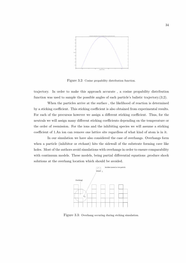
Figure 3.2: Cosine propability distribution function.
trajectory. In order to make this approach accurate , a cosine propability distribution
function was used to sample the possible angles of each particle’s balistic trajectory.(3.2).
When the particles arrive at the surface , the likelihood of reaction is determined
by a sticking coefficient. This sticking coefficient is also obtained from experimental results.
For each of the precursos however we assign a different sticking coefficient. Thus, for the
neutrals we will assign many different sticking coefficients depending on the temperature or
the order of reemission. For the ions and the inhibiting species we will assume a sticking
coefficient of 1.An ion can remove one lattice site regardless of what kind of atom is in it.
In our simulation we have also considered the case of overhangs. Overhangs form
when a particle (inhibitor or etchant) hits the sidewall of the substrate forming cave like
holes. Most of the authors avoid simulations with overhangs in order to ensure comparability
with continuum models. These models, being partial differential equations ,produce shock
solutions at the overhang location which should be avoided.
1
Incident neutral or ion particle
2
Overhang!
Figure 3.3: Overhang occuring during etching simulation.

35
In order to prevent overhangs from hanging we imping the following 2 additional
rules to our simulation:
1. if a depositing particle hits the sidewall ,it is allowed to slide down.
2. if an etchant etches the sidewall we remove the top lattice site of the x-coordinate
where the hit occured.
The following figures clarify the above mentioned procedure: 3.2. Whereas for the
deposition procedure, the incoming particle (1), hits the sidewall (2) and ”diffuses” to the
top of that column (3), in the etching simulation , the incoming etchant (1) doesnt remove
the cell where it actually hit (2), but the top cell of that column indeed (3).
1
2
3
Incident Inhibitor
(a) deposition
1
Incident neutral or ion particle
2
3
(b) etching
Figure 3.4: Monte Carlo procedure for modelling of etching or deposition processes.
The output of the program appart from statistical information , is the actual
surface at the end of the simulation written in a .dat file. This file looks like this:

36
Figure 3.5: view of a typical lattice outpute

37
Chapter 4
Dry isotropic etching using
reactive neutrals
4.1 Shadowing Effect
In this chapter, we will assume that the only precursors involved in the etching
process are neutrals, with a sticking propability of unity.
Geometrical Shadowing is a term used to characterize the effect of some areas of
the wafer receiving less incoming particle flux from the others because the are ”‘shadowed”’
by the surrounding areas of the wafer. Since we assume that our particles travel ballistically
from the bulk into the substrate, higher peaks receive significantly more flux than valleys,
since their line of sight angle into the ”‘sky”’ of particles above them is greater. See 4.1.
Shadowing is a non-local effect in the following sense: A big mountain-like struc-
ture inside the wafer shadows the entire area of the wafer. Thus, every point in the wafer
affects all the others. To add on, shadowing is a smoothing process with respect to the
roughening of the profile. Since hills are being etched more quickly than the valleys, all
height differences tend to diminish, leaving only the influence of the random effect of incom-
ing particles as the dominant roughening mechanism. This phenomena are cleary illustrated
in the following figures : 4.1
We will try to compare our simulation results with those of Drotar et all [25] in
order to validate our code. Their simulation however is three dimensional, and thus we
can’t explicitly though compare the outcome of our simluations . A time of 109 particles in

38
Figure 4.1: Shadowing effect
(a) rms vs time [25]
100
101
102
103
104
10−2
10−1
100
101
rms vs time
time (Latt units)
rms
(pix
els)
(b) rms vs time, our impementation
Figure 4.2: Surface Width vs Time for Shadowing Etching

39
the three dimensional simulation on a 1028× 1028 lattice can be said to be equivalent with√
109 particles on our 1024 lattice. However a qualitative comparison can be done to show
some important features.
Shadowing Etching is a stationary process, reaching an dynamic equilibrium
point.After the initial stochastically driven regime, rms becomes linearly dependent on
Log(t) which implies that β = 0. This is obviously seen in [25] simulation, but not quite on
our’s , since we find β to be small,β = 0.17 but not zero.
The height-height correlation functions (figure 4.1) strenthens our argument, since
for small distances they tend to overlap .This means that after some initial roughening
time, the small distance height differences remain the same, thus no mounded nor columnar
surfaces arise. In addition, the power spectral density functions show a clear peak near 0.6
which value scales with time as shown in 4.1.Roughness scales down with the sample size
very slowly because the interface is almost non rough and it is self similar. For an example
wafer see 4.3. Note the small roughness of the surface, clearly showing that shadowing
ethcing is a smoothing effect.
The etched depth is linear with time (figure 4.4),which means that the etching
occurs without any change due the surface.
0 200 400 600 800 1000 1200 1400 1600 1800 20004992
4994
4996
4998
5000
5002
5004
5006
5008
5010profile of the wafer
wafer size
heig
ht
Figure 4.3: Profile of the wafer,under shadowing etching,etched for 106 particles
Another comment could be made from the figures 4.1. The parameter α is small,

40
0 500 1000 1500 2000 2500 3000 3500 4000 4500 50005000
5500
6000
6500
7000
7500
8000
8500
9000
9500
10000etched depth vs time
time (Latt units)
Etc
hed
dept
h
Figure 4.4: Etched depth of the wafer,under shadowing etching
(a) hhcf evolution [25]
100
101
102
103
100
Height Heigth Correlation Function
r (in pixels)
hhcf
t=106 particles
t=2*106
t=4*106
t=6*106
t=8*106
Note the overapping!
(b) hhcf evolution, our impementation
Figure 4.5: hhcf evolution during shadowing etching.
due to the surface self affinity, and remain nearly constant throughout the procedure,showing
that the surface has reached a near-equilibrium state.
We are finally ready now to prove the existence of the FV scaling ansatz in the
case of shadowing etching. We have obtained the following results from our simulations:
α = 0.25, β = 0.17,1
z= 1.45
A quick division proves the FV scaling , within a 95 percent confidence interval.
In this paragraph , we dealt with the shadowing effect. For an etching process,
we proved that it has a smoothing effect on the surface. The resulting morphology

41
1 1.5 2 2.5 3 3.5 4 4.5 50.2
0.21
0.22
0.23
0.24
0.25
0.26
0.27
0.28
0.29
number of particles (106)
alph
a
evolution of alpha vs time
(a) α vs time
100
101
102
103
ξ evolution vs time
Number of particles (2*106)
/xi
y=2.7331x1.4425
(b) ξ vs time
Figure 4.6: Surface fractal parameters evolution under shadowing etching.
are non-rough, self-affine surfaces. Under no circumstances the shadow effect alone
can satisfactory explain the experimentally observed rough mounded surfaces,let alone the
increase of the rms of the surface with exposure time. We also proved the existence of
scaling, and more specifically, in agreement with past works (e.x [9]), FV scaling.
42
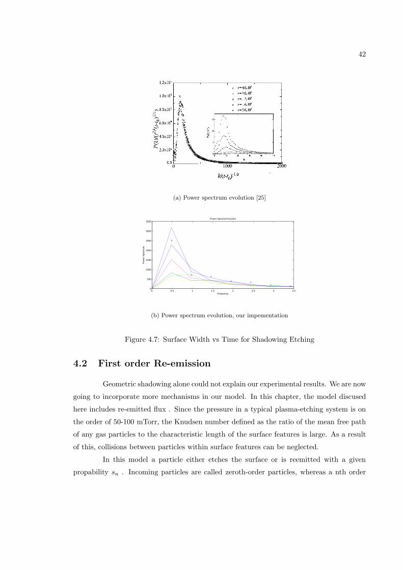
(a) Power spectrum evolution [25]
0 0.5 1 1.5 2 2.5 3 3.50
500
1000
1500
2000
2500
3000
3500Power Spectral Function
Frequency
Pow
er S
pect
rum
(b) Power spectrum evolution, our impementation
Figure 4.7: Surface Width vs Time for Shadowing Etching
4.2 First order Re-emission
Geometric shadowing alone could not explain our experimental results. We are now
going to incorporate more mechanisms in our model. In this chapter, the model discused
here includes re-emitted flux . Since the pressure in a typical plasma-etching system is on
the order of 50-100 mTorr, the Knudsen number defined as the ratio of the mean free path
of any gas particles to the characteristic length of the surface features is large. As a result
of this, collisions between particles within surface features can be neglected.
In this model a particle either etches the surface or is reemitted with a given
propability sn . Incoming particles are called zeroth-order particles, whereas a nth order

43
particle has been re-emitted n times.
The choice of the propabilities sn have a crucial effect on the etched profile and
its first and second order characteristics, therefore a thorough understanding of its effects
must be made.
In the case where the zeroth order sticking coefficient in near zero (s0 ≃ 0) and
the first is near unity (s1 ≃ 1) we have first order etching. In a similar fashion we will define
nth order etching if s0...n1≃ 0,sn ≃ 1.
Incident neutral or ion particle1
2
3
4
First reemission
Second reemission
Figure 4.8: illustration of a reemitted particle
The redistribution of the incoming flux is the result of the gas-solid interactions.
The solid surface imposes a boundary which affects the behaviour of the gas transport.
Therefire the redistribution heavily depends on surface conditions such as roughness , phys-
ical or chemical absorption, and surface chemical reaction.
We must therefore dwell upon the re-emission mode , which is actually controlled
by the p.d.f that assignes the particle’s new ballistic travell angle with respect to the surface
44
normal. There are many re-emission modes proposed,but we will confine ourselfes to the
cases of thermal and uniform re-emission.
1. Thermal re-emission means that all incoming particles reach thermal equilibrium with
the surface instantly and they are then re-emitted from the surface back to the plasma
bulk with a maxwellian distribution of velocities. Following the analysis of drotar et
al ([25]) we will use again a cosine distribution function for the angle of re-emission
with respect to the surface normal.
2. Uniform re-emission means that by using similar arguments as before we will treat
the re-emission angle as being uniformly distributed from −90o to 90o with respect to
the surface normal.
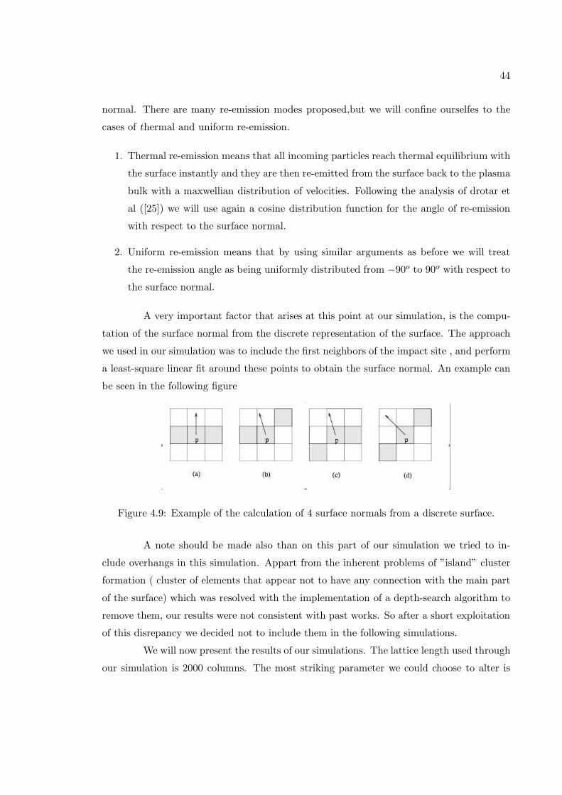
A very important factor that arises at this point at our simulation, is the compu-
tation of the surface normal from the discrete representation of the surface. The approach
we used in our simulation was to include the first neighbors of the impact site , and perform
a least-square linear fit around these points to obtain the surface normal. An example can
be seen in the following figure
Figure 4.9: Example of the calculation of 4 surface normals from a discrete surface.
A note should be made also than on this part of our simulation we tried to in-
clude overhangs in this simulation. Appart from the inherent problems of ”island” cluster
formation ( cluster of elements that appear not to have any connection with the main part
of the surface) which was resolved with the implementation of a depth-search algorithm to
remove them, our results were not consistent with past works. So after a short exploitation
of this disrepancy we decided not to include them in the following simulations.
We will now present the results of our simulations. The lattice length used through
our simulation is 2000 columns. The most striking parameter we could choose to alter is
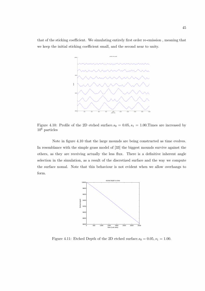
45
that of the sticking coefficient. We simulating entirely first order re-emission , meaning that
we keep the initial sticking coefficient small, and the second near to unity.
0 200 400 600 800 1000 1200 1400 1600 1800 20008500
9000
9500
10000profile of the wafer
wafer size
heig
ht
Figure 4.10: Profile of the 2D etched surface.s0 = 0.05, s1 = 1.00.Times are increased by106 particles
Note in figure 4.10 that the large mounds are being constructed as time evolves.
In resemblance with the simple grass model of [33] the biggest mounds survive against the
others, as they are receiving actually the less flux. There is a definitive inherent angle
selection in the simulation, as a result of the discretized surface and the way we compute
the surface nomal. Note that this behaviour is not evident when we allow overhangs to
form.
0 500 1000 1500 2000 2500 3000 35008600
8800
9000
9200
9400
9600
9800
10000etched depth vs time
time (Latt units)
Etc
hed
dept
h
Figure 4.11: Etched Depth of the 2D etched surface.s0 = 0.05, s1 = 1.00.
46
The etched depth (figure 4.11) is linear with time, after a very short initial regime
which is sublinear due to the fact that our initial surface is flat, and due to the very low s0
most particles are re-emitted back to the plasma bulk.
8500 8550 8600 8650 8700 8750 88000
50
100
150
200
250
300Histogram of the heights of the final profile
heights Bins
Num
ber
of h
eigh
ts in
the
bins
Figure 4.12: Heights distribution for the final profile after 8 · 106 particles.s0 = 0.05, s1 =1.00.
The heights density distribution are shown in figure 4.12. We must note that the
heights are quite uniformly distributed. This is a striking difference between these and the
experimentally observed ones, which have a distinct tail. This uniformity can be explained
from the fact that the slopes created from the mechanism we use can only create smooth
and small neighbooring columns height differences. In fact, identical mounds of different
size tend to evolve on the whole profile, with the same however slopes.
0 1000 2000 3000 4000 5000 60000
20
40
60
80
100
120
140
160
t in Latt units (Latt=2000 cells)
rms
rms(t) ,6000 Time units,S1=1,thermal reemission
S0=0.001
S0=0.005
S0=0.01
S0=0.03
S0=07
S0=0.10
S0=0.15
S0=0.001
S0=0.05
Figure 4.13: Rms for various first sticking coefficients,no overhangs
The fact that there is a clear difference in our simulations when overhangs are

47
0 1000 2000 3000 4000 5000 60000
20
40
60
80
100
120
rms(t) for S0=various S
1=0.95,including overhangs
t in Latt units (Latt=2000 cells)
rms
S0=0.005
S0=0.02
S0=0.01
S0=0.03
Figure 4.14: Rms for various first sticking coefficients,including overhangs
allowed to form is also seen from the 4.13 ,4.14.
There are two striking differences between the two simulations that are to be
noted:Firstly, the profile neglecting overhangs is much smoother than the one allowing
them. Secondly, rms seems to have a power law dependance with time with an exponent
β = 0.6 rather that unity. This behaviour is treated only when lowering the first sticking
coefficient by a magnitute of 7.
The reason for this phenomenon can be found in the fact that when overhangs are
formed, re-emitting particles tend to be trapped in the profiles local features , rather than
re-emitting globally among the profile, thus leading to an effective sticking coefficient much
larger than specified initially by the user. This disrepancy fades out when we decrease the
initial sticking coefficient,returning the effective value to the user-supplied one.
There are two important features about figure 4.15. The first is that even though
we decrease the first sticking coefficient as low as we can, we cannot get a hyperlinear
rms increase. Roughness generated from first order re-emission yields b ≈ 1. Secondly, it
makes evident that even small changes in the sticking coefficients have critical changes in
the surface roughness.
In figure 4.16 we follow the evolution of the height height correlation functions.
The overlapping of the functions is not very clear for the small length scales. To add on the
resemblance is obvious with those calculated by drotar (figure 4.17in [9].There is however
a nearly linear dependance of ξ as depicted from the study of these curves. finally the
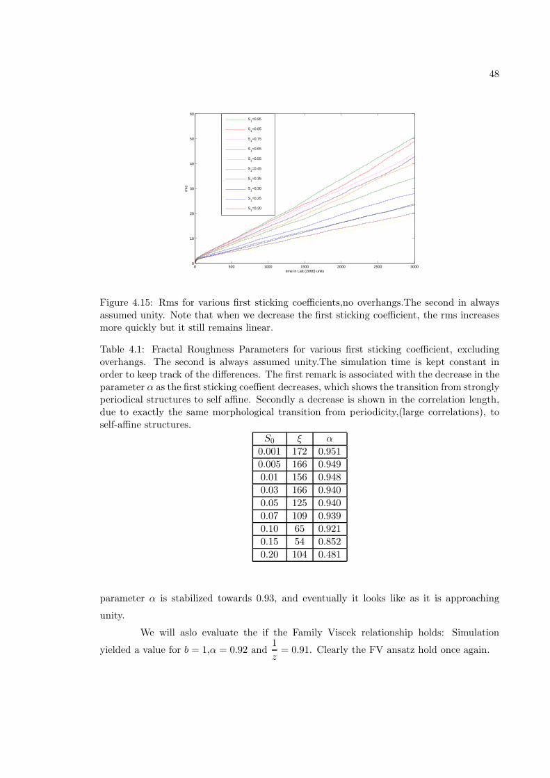
48
0 500 1000 1500 2000 2500 30000
10
20
30
40
50
60
time in Latt (2000) units
rms
S1=0.95
S1=0.85
S1=0.75
S1=0.65
S1=0.55
S1=0.45
S1=0.35
S1=0.30
S1=0.25
S1=0.20
Figure 4.15: Rms for various first sticking coefficients,no overhangs.The second in alwaysassumed unity. Note that when we decrease the first sticking coefficient, the rms increasesmore quickly but it still remains linear.
Table 4.1: Fractal Roughness Parameters for various first sticking coefficient, excludingoverhangs. The second is always assumed unity.The simulation time is kept constant inorder to keep track of the differences. The first remark is associated with the decrease in theparameter α as the first sticking coeffient decreases, which shows the transition from stronglyperiodical structures to self affine. Secondly a decrease is shown in the correlation length,due to exactly the same morphological transition from periodicity,(large correlations), toself-affine structures.
S0 ξ α
0.001 172 0.951
0.005 166 0.949
0.01 156 0.948
0.03 166 0.940
0.05 125 0.940
0.07 109 0.939
0.10 65 0.921
0.15 54 0.852
0.20 104 0.481
parameter α is stabilized towards 0.93, and eventually it looks like as it is approaching
unity.
We will aslo evaluate the if the Family Viscek relationship holds: Simulation
yielded a value for b = 1,α = 0.92 and1
z= 0.91. Clearly the FV ansatz hold once again.

49
Table 4.2: Fractal Roughness Parameters for various sticking coefficients.Note that we usea bigger first sticking coefficient than the second, which is the inverse of drotar et allsimulation.
S0 S1 ξ α
0.9 0.5 53 0.24
0.7 0.5 65 0.23
0.5 0.3 60 0.24
100
101
102
103
10−1
100
101
102
103
Height Heigth Correlation Function
r (in pixels)
hhcf
Figure 4.16: Height Height Correlation Functions,no overhangs.Time evolves per 106
particles.
4.3 Mixed order Re-emission
We have already tried to change the sticking coefficients and track the outcome
in section 4.2 . However, we sticked to the first-order re-emission mechanisms ,confining
ourselves about the range we could alter them.
In this section we will explore and try to map the effect of the sticking probabilities
when they change from the first hit to the second, but therein remain constant. The
following two figures (4.3)summarize all the information into two contour plots.
The x, y dimensions in the contours characterize the first and second sticking
coefficient respectively, with unity at the bottom right corner. We can therefore extract the
following information from the graphs:
1. Roughness instability as defined by drotar et all, a linear scaling of roughness with
respect to time (β = 1) is not found only in first order re-emission modes. A small

50
Figure 4.17: Height Height Correlation Functions,no overhangs.[9]
1 2 3 4 5 6 7 80.82
0.84
0.86
0.88
0.9
0.92
0.94α evolution
time (106 particles)
α va
lue
(a) α vs time
100
101.1
101.2
101.3
101.4
101.5
101.6
101.7
101.8
ξ evolution
time (106 particles)
ξ va
lue y=2.43x0.9108
(b) ξ vs time
Figure 4.18: Kinetic roughening
increase between the first and the second sticking coefficient, as long as the first is
small two, can result in roughness instability and exactly the same morphologies as
observed by drotar et al.
2. For small and constant sticking coefficients, we find β = 0.25, a scaling exponent in
agreement with the kuramoto-shivashinki equation, and for large times the same as

51
(a) Effect of sticking propabilities in the dynamic exponent
2 4 6 8 10 12 14 16 18 20
2
4
6
8
10
12
14
16
18
20
(b) Effect of sticking propabiliies in the etched Depth
Figure 4.19: sticking propabilities effect on etching parameters

52
0 1000 2000 3000 4000 5000 6000 7000 8000 9000 100000
0.5
1
1.5
2
2.5
3
3.5
4
4.5rms vs time
time (Latt units)
rms
(pix
els)
(a) rms vs time (linear plot)
100
101
102
103
104
10−2
10−1
100
101
rms vs time
time (Latt units)
rms
(pix
els)
(b) rms vs time (loglog plot)
the Kardar-Paris-Zhang (KPZ) equation.
3. The etched depth is more sensitive to the first coefficient, a results which is sound,
meaning that the biggest contribution to the etching comes from the direct flux.
We will also demonstrate the example of a constant sticking re-emission of 0.5.
As seen from 4.3 roughness is again linear with log(t) resulting in a very small
kinetic roughening exponent. The etching rate is constant , and finally the resulting profile
satisfies every criterion as to be characterized as self-affine as seen from the plots 4.20 and
4.3.
10−1
100
101
102
103
10−1
100
101
102
103
104
Power Spectral Function
Frequency
Pow
er S
pect
rum
(c) power spectrum (loglog plot)
0 0.2 0.4 0.6 0.8 1 1.2 1.4 1.6 1.8 20
500
1000
1500
2000
2500
3000
3500Power Spectral Function
Frequency
Pow
er S
pect
rum
(d) power spectrum (linear plot)
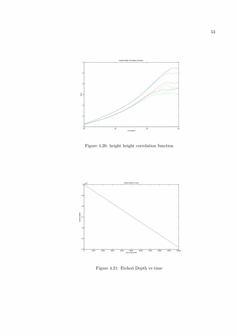
53
100
101
102
103
1
2
3
4
5
6
7Height Heigth Correlation Function
r (in pixels)
hhcf
Figure 4.20: height height correlation function
0 1000 2000 3000 4000 5000 6000 7000 8000 9000 100001.4
1.5
1.6
1.7
1.8
1.9
2x 10
4 etched depth vs time
time (Latt units)
Etc
hed
dept
h
Figure 4.21: Etched Depth vs time
54
Chapter 5
Ion enchanced etching
Typically in a plasma reactor, apart from the existence of reactive neutrals, ionized
particles are present. These particles activate the bonds between the surface atoms, and
thus enhancing the effect of the neutrals.
In our simulation, we will assume that the ions travel anisotropically, following
vertical trajectories. When they collide with the surface , they will always etch one lattice
site. We will gradually increase the ions to neutral ratio (IN ratio) on the surface and track
down the differences.
If we assumed that the surface was hit only with ions, it would be easy to show [3]
that the rms would yield a β =1
2, the signature of a random walk process.This additional
random effect that the ions introduce will brake down the power law of the kinetic rough-
ening. They ions will initiate random roughening in addition to the standard roughening
occurring by the re-emitted neutrals.
In the following simulations, we have used a 2000 column lattice. The sticking
coefficient for the neutrals , is set to be constant for all re-emissions and equal with 0.2.
5.1 IN ration 1:100
A IN ration of1
100is assumed in this simulation. Not much to be said though,
since the ions only have a very mild effect, not noticeable on the surface characteristics.

55
0 500 1000 1500 2000 2500 3000 3500 4000 4500 50000
0.5
1
1.5
2
2.5
3
3.5
4rms vs time
time (Latt units)
rms
(pix
els)
(a) Rms evolution vs time
100
101
102
103
100
Height Heigth Correlation Function
r (in pixels)
hhcf
(b) hhcf evolution
0 200 400 600 800 1000 1200 1400 1600 1800 20009180
9185
9190
9195
9200
9205
9210profile of the wafer
wafer size
heig
ht
(c) Final profile
9180 9185 9190 9195 9200 9205 92100
100
200
300
400
500
600histogram of the heights of the etched surface
Heights
Num
ber
of e
ntrie
s in
the
bins
(d) Height distribution for the
final profile
Figure 5.1: Ion enchanced etching IN ratio=1:100
5.2 IN ration 2:100
5.3 IN ration 5:100
5.4 IN ration 10:100
We must note that the effect of the ions are evident on the etch rate. Since they
have a sticking coefficient of unity, they contribute more on the surface etch. Moreover, the

56
0 200 400 600 800 1000 1200 1400 1600 1800 20009100
9200
9300
9400
9500
9600
9700
9800
9900profile of the wafer
wafer size
heig
ht
Figure 5.2: Profile evolution
more we increase the IN ratio, the more the height-height correlation function tends not to
follow a power law, as in the case of isotropic etching purely by neutrals, but is affected by
the random character of the ions.

57
0 500 1000 1500 2000 2500 3000 3500 40000
0.5
1
1.5
2
2.5
3
3.5
4rms vs time
time (Latt units)rm
s (p
ixel
s)
(a) rms vs time
100
101
102
103
100
Height Heigth Correlation Function
r (in pixels)
hhcf
(b) hhcf evolution
0 200 400 600 800 1000 1200 1400 1600 1800 20008880
8885
8890
8895
8900
8905
8910profile of the wafer
wafer size
heig
ht
(c) final proflie
8880 8885 8890 8895 8900 8905 89100
100
200
300
400
500
600
Num
ber
of e
ntrie
s in
the
bins
histogram of the heights of the etched surface
Heights
(d) heights distribution for the
final profile
Figure 5.3: Ion enchanced etching IN ratio=2:100

58
0 200 400 600 800 1000 1200 1400 1600 1800 20008800
9000
9200
9400
9600
9800
10000profile of the wafer
wafer size
heig
ht
Figure 5.4: A Profile evolution
0 500 1000 1500 2000 2500 3000 3500 40000
0.5
1
1.5
2
2.5
3
3.5
4rms vs time
time (Latt units)
rms
(pix
els)
(a) sc = 0.20
0 200 400 600 800 1000 1200 1400 1600 1800 20008785
8790
8795
8800
8805
8810
8815profile of the wafer
wafer size
heig
ht
(b) sc = 0.20
8785 8790 8795 8800 8805 8810 88150
50
100
150
200
250
300
350
400
450
500histogram of the heights of the etched surface
Heights
Num
ber
of e
ntrie
s in
the
bins
(c) sc = 0.20
Figure 5.5: Ion enchanced etching IN ratio=5:100.

59
0 500 1000 1500 2000 2500 3000 3500 40000
0.5
1
1.5
2
2.5
3
3.5
4rms vs time
time (Latt units)
rms
(pix
els)
(a) sc = 0.20
0 200 400 600 800 1000 1200 1400 1600 1800 20008634
8636
8638
8640
8642
8644
8646
8648
8650
8652
8654profile of the wafer
wafer size
heig
ht
(b) sc = 0.20
8634 8636 8638 8640 8642 8644 8646 8648 8650 8652 86540
50
100
150
200
250
300
350
400
450
Heights
Num
ber
of e
ntrie
s in
the
bins
histogram of the heights of the etched surface
(c) sc = 0.20
Figure 5.6: Ion enchanced etching IN ratio=10:100
0 500 1000 1500 2000 2500 3000 3500 40008600
8800
9000
9200
9400
9600
9800
10000etched depth vs time
time (Latt units)
Etc
hed
dept
h
2% ions1% ions5%ions10%ions
Figure 5.7: Profile evolution
60
Chapter 6
An Etching model using Inhibitors
In this section we will study the effects of impurities in the film synthesis.
Surface contamination plays a very important role in dry etching reactions ei-
ther because new layers can deposit on the samples or because the structure and chemical
composition of existing surfaces can be modified.
If one has to tell the story of contaminants and of non volatile layers in the chem-
istry of etching processes and in the overall etching kinetics, a fairly good example to start
with is that of aluminum etching. Aluminum thin films are always covered by an inert
surface layer of Al2O3, which causes the well known delay between discharge ignition and
the etching process start (induction time).
To remove the surface contaminant layer strong ion bombardment and/or the
appropriate chemistry are required (e.g. CC14 or BCI3 addition to the feed). When the
induction time is over, etching can proceed in chlorine by the reaction of chlorine molecules
and/or atoms as a function of the experimental conditions.
The thickness of this deposit increases with time particularly at low temperature
(film deposition is generally favoured by low temperatures). The contaminant layer does
interfere with the etching kinetics since it acts as a barrier to the ingoing etchant species
and/or the out-going etch products. At higher temperatures the phenomenon is much
reduced because the thickness of the contaminant film becomes very small. This means
that what is usually measured is not the real chemical Al-etch rate, that is to say the value
in the absence of barrier films of contaminant chlorocarbon polymer and etch products, but
an ’apparent’ physico-chemical rate which includes through-film diffusion effects.
The presence of a contaminant film, called inhibitor or side wall blocking agent,

61
is often required to promote directional etching as in the case of tungsten dry etching in
fluorocarbon mixtures. In this case in situ Auger spectroscopy has been utilized to study
the effect of low energy ion bombardment on the formation of a fluorocarbon contaminant
film in a triode-reactor fed with CF4 − H2 (and CF4 − 02) [11]. It has been shown that
on the surfaces interested by ion bombardment the etching process occurs even at high
hydrogen concentration, conditions known to be suitable for deposition and not for etching.
These surfaces, in fact, are not completely covered by fluoropolymers and bare tungsten is
available for reaction with fluorine atoms.
On the other hand, surfaces which are not subjected to ion bombardment are
covered by a thick film of contaminant and the etching process completely stops.
The formation of contaminant layers is not only a peculiarity of those processes
characterized by low volatile etch products and/or polymerizing etching mixtures as in the
previous examples.
During titanium dry etching in CF4 − 02 , for instance, the substrate surface is
covered by a thick hyperfluorinated layer of titanium fluorides [44], which is able to trap
some fluorine (F2, and/or F−). The thickness of this layer strongly depends on the working
conditions but it has never been found to be less than 5 − 6nm. The presence of trapped
species in the surface of etched samples has also been revealed in the case of tungsten etching
in fluorine containing plasmas, in this case the surface contains WF4, WF5, and as trapped
species WF6 (the etch product) and F2(0r F−).
Bearing all the previous in mind, we will assume now that there will be an incoming
flux of inhibiting species, as well as a flux of ions.
There are now 3 species in our simulation.The new rules for the simulation are
now:
1. Etchants (neutral particles)
• They travel ballistically with a cosine angle distribution function.
• They are re-emmitted with a given constant propability (e.x s0 = s1 = . . . =
s50 = 0.2).
• They are re-emmitted with a cosine angle distribution function around the surface
normal.
• They treat inhibitors as non-etchable lattice sites.

62
2. Ions
• They travel anisotropically,with a gaussian angle distribution with s.t.d=2.5o.
• They remove one inhibitor or one silicon lattice site.
• They are never re-emmitted from the surface.
3. Inhibitors
• They travel ballistically with a cosine angle distribution function.
• They are rarely re-emmitted with a given constant propability (e.x s0 = s1 =
. . . = s50 = 0.8).
• They are re-emmitted with a cosine angle distribution function around the surface
normal.
No overhangs are allowed to form. Thus, when an inhibitor deposits in a way that
allows an overhang to be formed, we allow him to slide down to the columns top.
There is a new quanity which has to be defined ,since there are more than one
species involved in the simulation and are present on the film. We shall define this new
parameter as Surface Coverage and it will be the ratio between the inhibitors and the
neutrals evident on the top pixel of the surface profile.
We will present an example using figure 6.1. There are 12 top lattice sites. Out
of these 12 , 5 of them are covered with an inhibitor. Therefore coverage =5
12= 0.41667.
Notice that the existence of more inhibiting species,not on the top site of each column, does
not alter the surface coverage.
Figure 6.1: An illustration of the calculation of the surface coverage.

63
We will know present a variety of etched profiles using our inhibitor model. Each
column shows a fixed sticking coeffient for the neutrals. Each line shows a fixed ratio of
incoming particles. Thus, the first line shows a flux combining of 0.5 percent inhibitors and
1 percent ions. The second line shows a flux combining of 1 percent inhibitors and 2 percent
ions. Finally the third shows a flux combining of 2 percent inhibitors and 3 percent ions.
(a) sc = 0.10 (b) sc = 0.15 (c) sc = 0.20
(d) sc = 0.10 (e) sc = 0.15 (f) sc = 0.20
(g) sc = 0.10 (h) sc = 0.15 (i) sc = 0.20
Figure 6.2: Profile of the 2D etched surfaces, using inhibitors.

64
(a) sc = 0.10 (b) sc = 0.15 (c) sc = 0.20
(d) sc = 0.10 (e) sc = 0.15 (f) sc = 0.20
(g) sc = 0.10 (h) sc = 0.15 (i) sc = 0.20
Figure 6.3: Rms roughness of the 2D etched surfaces,using inhibitors.

65
(a) sc = 0.10 (b) sc = 0.15 (c) sc = 0.20
(d) sc = 0.10 (e) sc = 0.15 (f) sc = 0.20
(g) sc = 0.10 (h) sc = 0.15 (i) sc = 0.20
Figure 6.4: Etched Depth of the 2D etched surfaces,using inhibitors.

66
(a) sc = 0.10 (b) sc = 0.15 (c) sc = 0.20
(d) sc = 0.10 (e) sc = 0.15 (f) sc = 0.20
(g) sc = 0.10 (h) sc = 0.15 (i) sc = 0.20
Figure 6.5: coverage of the 2D etched surfaces,No Overhangs,using inhibitors.

67
(a) sc = 0.10 (b) sc = 0.15 (c) sc = 0.20
(d) sc = 0.10 (e) sc = 0.15 (f) sc = 0.20
(g) sc = 0.10 (h) sc = 0.15 (i) sc = 0.20
Figure 6.6: HHCF of the 2D etched surfaces,No Overhangs,using inhibitors.
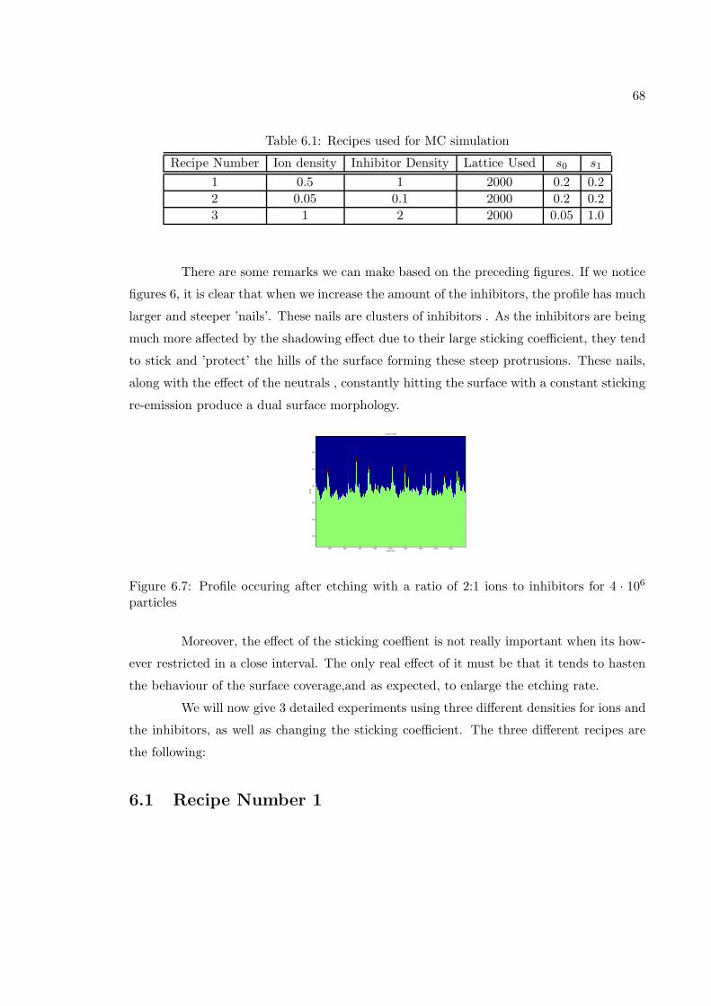
68
Table 6.1: Recipes used for MC simulation
Recipe Number Ion density Inhibitor Density Lattice Used s0 s1
1 0.5 1 2000 0.2 0.2
2 0.05 0.1 2000 0.2 0.2
3 1 2 2000 0.05 1.0
There are some remarks we can make based on the preceding figures. If we notice
figures 6, it is clear that when we increase the amount of the inhibitors, the profile has much
larger and steeper ’nails’. These nails are clusters of inhibitors . As the inhibitors are being
much more affected by the shadowing effect due to their large sticking coefficient, they tend
to stick and ’protect’ the hills of the surface forming these steep protrusions. These nails,
along with the effect of the neutrals , constantly hitting the surface with a constant sticking
re-emission produce a dual surface morphology.
lattice site
heig
ht
surface profile
200 400 600 800 1000 1200 1400 1600 1800
450
500
550
600
650
700
Figure 6.7: Profile occuring after etching with a ratio of 2:1 ions to inhibitors for 4 · 106
particles
Moreover, the effect of the sticking coeffient is not really important when its how-
ever restricted in a close interval. The only real effect of it must be that it tends to hasten
the behaviour of the surface coverage,and as expected, to enlarge the etching rate.
We will now give 3 detailed experiments using three different densities for ions and
the inhibitors, as well as changing the sticking coefficient. The three different recipes are
the following:
6.1 Recipe Number 1
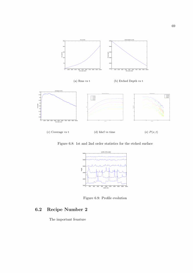
69
0 1000 2000 3000 4000 5000 6000 7000 8000 9000 100000
50
100
150
200
250rms vs time
time (Latt units)
rms
(pix
els)
(a) Rms vs t
0 1000 2000 3000 4000 5000 6000 7000 8000 9000 100003500
4000
4500
5000
5500
6000etched depth vs time
time (Latt units)
Etc
hed
dept
h
(b) Etched Depth vs t
0 1000 2000 3000 4000 5000 6000 7000 8000 9000 100000
0.05
0.1
0.15
0.2
0.25
0.3
0.35
0.4
0.45
0.5coverage vs time
time (latt units)
Cov
erag
e
(c) Coverage vs t
100
101
102
103
100
101
102
103
Height Heigth Correlation Function
r (in pixels)
hhcf
20m particles
16m particles
12m particles
8m particles
4m particles
2m particles
(d) hhcf vs time
10−1
100
101
102
101
102
103
104
105
106
107
Power Spectral Function
Frequency
Pow
er S
pect
rum
20m particles16m particles12m particles8m particles4m particles2m particles
(e) P (x, t)
Figure 6.8: 1st and 2nd order statistics for the etched surface
0 200 400 600 800 1000 1200 1400 1600 1800 20003500
4000
4500
5000
5500
6000profile of the wafer
wafer size
heig
ht
Figure 6.9: Profile evolution
6.2 Recipe Number 2
The important feuature
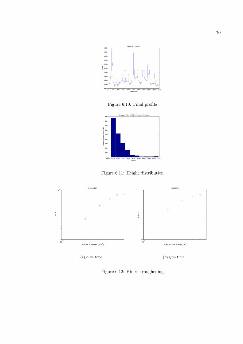
70
0 200 400 600 800 1000 1200 1400 1600 1800 20004450
4500
4550
4600
4650
4700
4750
4800
4850
4900
4950profile of the wafer
wafer size
heig
ht
Figure 6.10: Final profile
4450 4500 4550 4600 4650 4700 4750 4800 4850 4900 49500
100
200
300
400
500
600
700
800
900histogram of the heights of the etched surface
Heights
Num
ber
of e
ntrie
s in
the
bins
Figure 6.11: Height distribution
100
100
α evolution
Number of particles (4*106)
α va
lue
(a) α vs time
100
101
Number of particles (2*106)
ξ va
lue
ξ evolution
(b) ξ vs time
Figure 6.12: Kinetic roughening
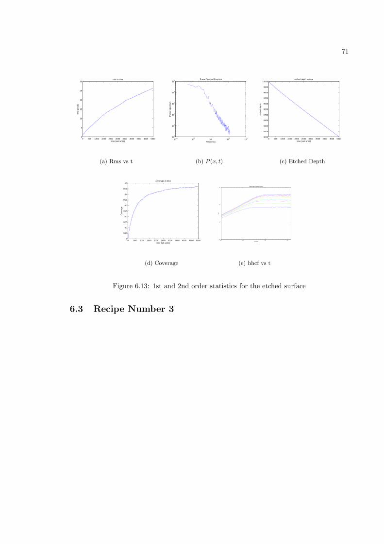
71
0 500 1000 1500 2000 2500 3000 3500 4000 4500 50000
5
10
15
20
25
30rms vs time
time (Latt units)
rms
(pix
els)
(a) Rms vs t
10−1
100
101
102
103
100
101
102
103
104
105
Power Spectral Function
Frequency
Pow
er S
pect
rum
(b) P (x, t)
0 500 1000 1500 2000 2500 3000 3500 4000 4500 50009000
9100
9200
9300
9400
9500
9600
9700
9800
9900
10000etched depth vs time
time (Latt units)
Etc
hed
dept
h
(c) Etched Depth
0 500 1000 1500 2000 2500 3000 3500 4000 4500 50000
0.05
0.1
0.15
0.2
0.25
0.3
0.35
0.4
0.45
0.5coverage vs time
time (latt units)
Cov
erag
e
(d) Coverage
100
101
102
103
10−1
100
101
102
Height Heigth Correlation Function
r (in pixels)
hhcf
(e) hhcf vs t
Figure 6.13: 1st and 2nd order statistics for the etched surface
6.3 Recipe Number 3
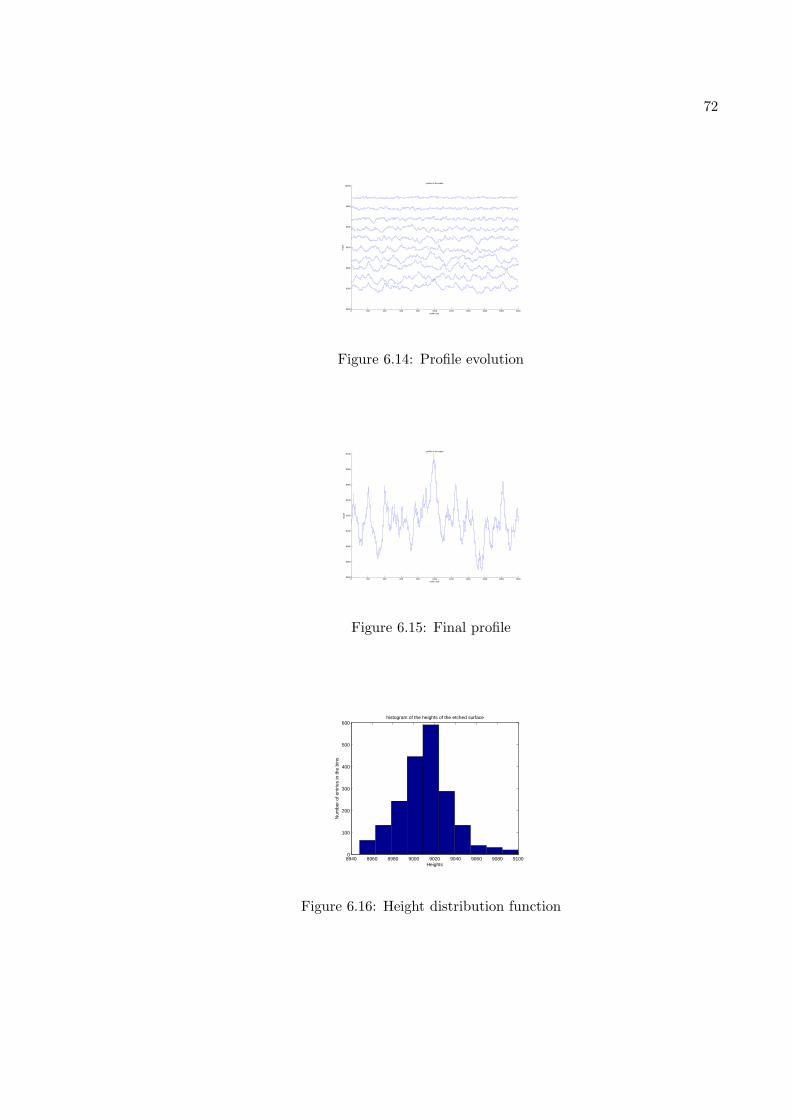
72
0 200 400 600 800 1000 1200 1400 1600 1800 20008800
9000
9200
9400
9600
9800
10000profile of the wafer
wafer size
heig
ht
Figure 6.14: Profile evolution
0 200 400 600 800 1000 1200 1400 1600 1800 20008940
8960
8980
9000
9020
9040
9060
9080
9100profile of the wafer
wafer size
heig
ht
Figure 6.15: Final profile
8940 8960 8980 9000 9020 9040 9060 9080 91000
100
200
300
400
500
600histogram of the heights of the etched surface
Heights
Num
ber
of e
ntrie
s in
the
bins
Figure 6.16: Height distribution function

73
100
101
102
103
104
10−3
10−2
10−1
100
101
102
rms vs time
time (Latt units)
rms
(pix
els)
(a) Rms vs t
0 500 1000 1500 2000 25009200
9300
9400
9500
9600
9700
9800
9900
10000etched depth vs time
time (Latt units)
Etc
hed
dept
h
(b) Etched Depth
0 500 1000 1500 2000 25000
0.05
0.1
0.15
0.2
0.25
0.3
0.35
0.4
0.45
0.5coverage vs time
time (latt units)
Cov
erag
e
(c) Coverage vs t
100
101
102
103
100
101
102
Height Heigth Correlation Function
r (in pixels)
hhcf
(d) hhcf vs t
Figure 6.17: 1st and 2nd order statistics for the etched surface
0 200 400 600 800 1000 1200 1400 1600 1800 20009100
9200
9300
9400
9500
9600
9700
9800
9900profile of the wafer
wafer size
heig
ht
Figure 6.18: Profile evolution
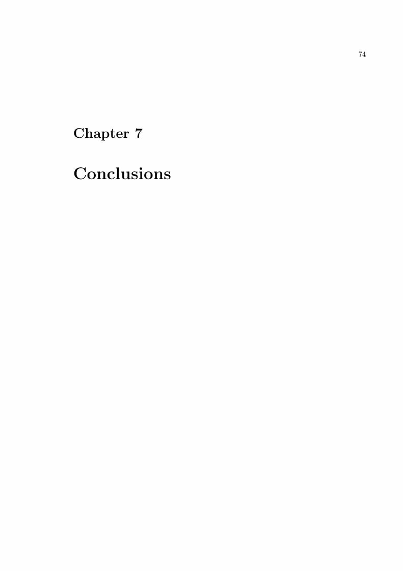
74
Chapter 7
Conclusions
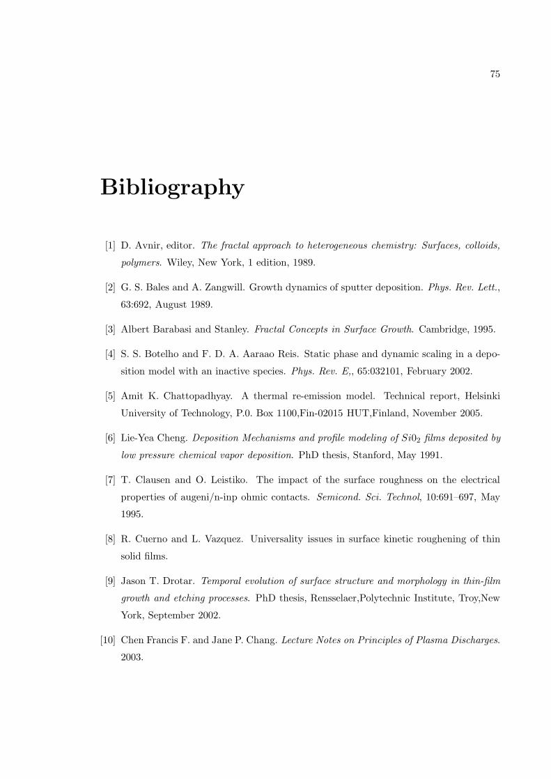
75
Bibliography
[1] D. Avnir, editor. The fractal approach to heterogeneous chemistry: Surfaces, colloids,
polymers. Wiley, New York, 1 edition, 1989.
[2] G. S. Bales and A. Zangwill. Growth dynamics of sputter deposition. Phys. Rev. Lett.,
63:692, August 1989.
[3] Albert Barabasi and Stanley. Fractal Concepts in Surface Growth. Cambridge, 1995.
[4] S. S. Botelho and F. D. A. Aaraao Reis. Static phase and dynamic scaling in a depo-
sition model with an inactive species. Phys. Rev. E,, 65:032101, February 2002.
[5] Amit K. Chattopadhyay. A thermal re-emission model. Technical report, Helsinki
University of Technology, P.0. Box 1100,Fin-02015 HUT,Finland, November 2005.
[6] Lie-Yea Cheng. Deposition Mechanisms and profile modeling of Si02 films deposited by
low pressure chemical vapor deposition. PhD thesis, Stanford, May 1991.
[7] T. Clausen and O. Leistiko. The impact of the surface roughness on the electrical
properties of augeni/n-inp ohmic contacts. Semicond. Sci. Technol, 10:691–697, May
1995.
[8] R. Cuerno and L. Vazquez. Universality issues in surface kinetic roughening of thin
solid films.
[9] Jason T. Drotar. Temporal evolution of surface structure and morphology in thin-film
growth and etching processes. PhD thesis, Rensselaer,Polytechnic Institute, Troy,New
York, September 2002.
[10] Chen Francis F. and Jane P. Chang. Lecture Notes on Principles of Plasma Discharges.
2003.
76
[11] J.W. Coburn F. Fracassi. J. Appl.Phys., 63:1758, 1998.
[12] F. Family and T. Viscek. Mechanisms for plasma and reactive ion etch-front roughen-
ing. J. Phys. A, 18:L75, 1985.
[13] Gil A. Farias and Alexei A. Maradudin. Surface plasmons on a randomly rough surface.
Phys. Rev. B, 28:5675–5687, November 1983.
[14] D. L. Flamm and V. M. Donnelly. Plasma Chem. Plasma Process. 1981.
[15] P.G.de Gennes. Wetting: statics and dynamics. Rev. Mod. Phys., 57:827–863, July
1985.
[16] G.Palasantzas and J. Barnas. Surface-roughness fractality effects in electrical con-
ductivity of single metallic and semiconducting films. Phys. Rev. B, 56:7726–7731,
September 1997.
[17] Jean-Jacques Greffet. Theoretical model of the shift of the brewster angle on a rough
surface. Opt. Lett., 17:238, 1992.
[18] M. J. Gordon T. A. Moore T. K. Minton G.S Hwang, C. M. Anderson and K.P. Giapis.
Gas-surface dynamics and profile evolution during etching of silicon. Physical review
letters, 77(14):3049–3052, September 1996.
[19] W. Wang H. F. El-Nashar and Hilda A Cerdeira. Surface growth kinetics and mor-
phological structural transition in a (2+1)-dimensional deposition model. J. Phys:
Condens. Matter, 8:3271–3283, December 1996.
[20] H. K. Kim H. You, R. P. Chiarello and K. G. Vandervoort. X-ray reflectivity and
scanning-tunneling-microscope study of kinetic roughening of sputter-deposited gold
films during growth. Phys. Rev. Lett., 70:2900–2903, May 1993.
[21] C. Roland J. H. Yao and H. Guo. Interfacial dynamics with long-range screening. Phys.
Rev. A, 45:3903–3912, March 1992.
[22] T.M. Lu J. T. Drotar, Y.P. Zhao and G.C. Wang. Mechanisms for plasma and reactive
ion etch-front roughening. Phys. Rev. B, 61:3012–3021, January 2000.
[23] T.M. Lu J. T. Drotar, Y.P. Zhao and G.C. Wang. Surface roughening in shadowing
growth and etching in 2+1 dimensions. Phys. Rev. B, 62:2118–2125, July 2000.
77
[24] T.M. Lu J. T. Drotar, Y.P. Zhao and G.C. Wang. Surface roughening in low-pressure
chemical vapor deposition. Phys. Rev. B, 64:125411, September 2001.
[25] T.-M. Lu Jason T. Drotar, Y.-P. Zhao and G.-C. Wang. Mechanisms for plasma and
reactive ion etch-front roughening. Phys. Rev. B, 61:3012–3020, January 2000.
[26] T.-M. Lu Jason T. Drotar, Y.-P. Zhao and G.-C. Wang. Mechanisms for plasma and
reactive ion etch-front roughening. Phys. Rev. B, 61:3012–3020, January 2000.
[27] Weidong Jin. Study of Plasma-Surface Kinetics and Feature Profile Simulation of
Poly-silicon Etching in Cl2/HBr plasmas. PhD thesis, MIT, December 2004.
[28] J.M. Lopez J.J. Ramasco and M.A. Rodriguez. Generic dynamic scaling in kinetic
roughening. Phys. Rev. Lett, 84:2199, March 2000.
[29] M.A. Rodriguez J.M. Lopez and R. Cuerno. Power spectrum scaling in anomalous
kinetic roughening of surfaces. Physica A, 246:329–347, 1997.
[30] K.A.O’Donnell and R.Torre. Second-harmonic generation from a strongly rough metal
surface. Optics Commun., 184:341–344, 1997.
[31] David Y. K. Ko and Flavio Seno. Simulations of deposition growth models in vari-
ous dimensions: The possible importance of overhangs. Phys. Rev. E, 50(3):R1741,
September 1994.
[32] H. Konig and T. Helwig. Optik (Stuttgart), 6:111, 1950.
[33] J. Krug and P. Meakin. Scaling properties of the shadowing model for sputter deposi-
tion. Phys. Rev. E, 47(1):R17–R20, January 1993.
[34] Vivek K.Singh and Eric S. G. Shaqfeh. Effect of surface re-emission on the surface
roughness of film growth in lpcvd. J. Vac. Sci. Technol. A, 11(6):557, 1993.
[35] C. L. Standley L. l. Maissel, R. E. Jones. Re-emission of sputtered sio2 during growth
and its relation to film quality. IBM J. RES. DEVELOP., 14:176–181, 1970.
[36] F. Ladouceur and J. D. Love. Silica-based Buried Channel Waveguides and Devices.
Chapman and Hall, London, 1996.

78
[37] A. Michael Lieberman and Allan J. Lichtenberg. Principles of Plasma Discharges and
Materials Processing. Wiley, 2005.
[38] J.M. Lopez. Phys. Rev. Lett, 83:4594, 1999.
[39] R. Cuerno M. Castro M. Jergel M. A. Auger, L.Vazquez and O. Sanchez. Intrinsic
anomalous surface roughening of tin films deposited by reactive sputtering. Phys. Rev.
B, 73:045436, January 2006.
[40] T. Leskova A. Maradudin M. Leyva-Lucero, E. Mendez and J. Lu. Multiple-scattering
effects in the second-harmonic generation of light in reflection from a randomly rough
metal surface. Opt. Lett., 21:1809, 1996.
[41] A. P. Maharowala. Dynamics of Ion-assisted Etching. PhD thesis, MIT, 1999.
[42] G. Oehrlein. Handbook of Plasma Processing Technology. Noyes Publications, 1990.
[43] H.-N. Yang Q. Jiang and G.-C. Wang. Effect of interface roughness on hysteresis loops
of ultrathin co films from 2 to 30 ml on cu(001) surfaces. Surf.Sci., 373(2-3):181–194,
March 1997.
[44] C. Pacifico R. d’Agostino, F. Fracassi and P. Capezzuto. J. Appl. Phys., 71:462, 1992.
[45] R. Bruinsma R. P. U. Karunasiri and J. Rudnick. Karunasiri, bruinsma, and rudnick
reply. Phys. Rev. Lett., 63:693, August 1989.
[46] R. Bruinsma R. P. U. Karunasiri and J. Rudnick. Thin-film growth and the shadow
instability. Phys. Rev. Lett., 62:788, 1989.
[47] O. Vatel D. Henry E. Andre P. Dumas F. Salvan R. Petri, P. Brault. Silicon roughness
induced by plasma etching. J. Appl. Phys., 75:7498, June 1994.
[48] Mark A. Chonko Rama I. Hegde and Philip J. Tobin. Effect of silicon substrate micro-
roughness on gate oxide quality. J. Vac. Sci. Technol. B, 14:3299–3304, 1996.
[49] E. Stanley et. al. R.Cuerno, H.A.Makse. Stochastic model for surface erosion via
ion sputtering : Dynamical evolution from ripple morphology to rough morphology.
Physical Review Letters, 75(24):4464–4467, December 1995.
79
[50] R. Lamendola R.d’Agostino, F. Fracassi. The chemistry of etching and deposition
processes. Pure and Appl.Chem., 66(6):1185–1194, 1994.
[51] Fabio D. A. Aaraao Reis. Depinning transitions in interface growth models. Brazilian
Journal of Physics, 33(3):501, September 2003.
[52] Christopher Roland and Hong Guo. Interface growth with a shadow instability. Phys.
Rev. Lett., 66:2104–2107, April 1991.
[53] M. Saillard and D. Maystre. Scattering by metallic and dielectric rough surfaces: an
integral method and its applications. Proc. SPIE, 1319:594, 1990.
[54] M. Santos and W.Figueiredo. Growth surface model with non active sites. Brazilian
Journal of Physics, 34:429, June 2004.
[55] Ernst Sclomann. Demagnetizing fields in thin magnetic films due to surface roughness.
Journal of Applied Physics, 41(4):1617–1622, 1970.
[56] Petrus Gerardus Maria Sebel. Dynamics of Ion-assisted Etching. PhD thesis, University
of Eindhoven, December 1999.
[57] T. Smy S.K. Dew and M.J. Brett. Simulation of the microstructure of chemical vapor
deposited refractory thin fimls. J. Vac. Sci. Technol. B, 10(2):618, 1992.
[58] R. Eklund E.A. Karunasiri R.P.U. Rudnick J. Zangwill A. Steven Bales, G. Bruinsma.
Growth and erosion of thin solid films. Science, 249(4966):264–268, July 1990.
[59] Chao Tang and Shoudan Liang. Patterns and scaling properties in a ballistic deposition
model. Phys. Rev. Lett., 71:2792, October 1993.
[60] Jose Ignacio Ulacia-Fresnedo. Theoretical and experimnetal considerations necessary
to build a dry-etching process simulator. PhD thesis, Stanford, June 1988.
[61] W. Wang and Hilda A. Cerdeira. Surface growth of two kinds of particle deposition
models. Phys. Rev. E, 52:6308, December 1995.
[62] G.-C. Wang Y.-P. Zhao, Jason T. Drotar and T.-M. Lu. Roughening in plasma etch
fronts of si(100). Phys. Rev. Lett., 82:4882–4885, June 1999.

80
[63] S. Yim and T.S. Jones. Anomalous scaling behavior and surface roughening in molec-
ular thin film deposition. Phys. Rev. B, 73:161305, April 2006.
[64] Yiping Zhao. In-plane light scattering from fractal surfaces-principles and experiments.
PhD thesis, Rensselaer,Polytechnic Institute, Troy,New York, June 1999.

81
Appendix A
Some Ancillary Stuff
Ancillary material should be put in appendices, which appear after the bibliogra-
phy.