Monochromators and Aberration Correctors: Taking EELS to
7
Journal of Physics: Conference Series OPEN ACCESS Monochromators and Aberration Correctors: Taking EELS to New Levels of Energy and Spatial Resolution To cite this article: N D Browning et al 2006 J. Phys.: Conf. Ser. 26 014 View the article online for updates and enhancements. You may also like Super-resolution X-ray imaging with hybrid pixel detectors using electromagnetic source stepping T. Dreier, U. Lundström and M. Bech - Simulation study of spatial resolution and sensitivity for the tapered depth of interaction PET detectors for small animal imaging Sara St James, Yongfeng Yang, Spencer L Bowen et al. - Quasistatic zooming for regional hyperthermia treatment planning J B Van de Kamer, A A C De Leeuw, H Kroeze et al. - Recent citations Characterizing Localized Surface Plasmons Using Electron Energy-Loss Spectroscopy Charles Cherqui et al - Performances of an 80–200 kV microscope employing a cold-FEG and an aberration-corrected objective lens Christian Ricolleau et al - Damien Alloyeau - This content was downloaded from IP address 45.177.200.218 on 05/01/2022 at 08:09
Transcript of Monochromators and Aberration Correctors: Taking EELS to
Journal of Physics Conference Series
OPEN ACCESS
Monochromators and Aberration CorrectorsTaking EELS to New Levels of Energy and SpatialResolutionTo cite this article N D Browning et al 2006 J Phys Conf Ser 26 014
View the article online for updates and enhancements
You may also likeSuper-resolution X-ray imaging with hybridpixel detectors using electromagneticsource steppingT Dreier U Lundstroumlm and M Bech
-
Simulation study of spatial resolution andsensitivity for the tapered depth ofinteraction PET detectors for small animalimagingSara St James Yongfeng Yang SpencerL Bowen et al
-
Quasistatic zooming for regionalhyperthermia treatment planningJ B Van de Kamer A A C De Leeuw HKroeze et al
-
Recent citationsCharacterizing Localized SurfacePlasmons Using Electron Energy-LossSpectroscopyCharles Cherqui et al
-
Performances of an 80ndash200 kVmicroscope employing a cold-FEG and anaberration-corrected objective lensChristian Ricolleau et al
-
Damien Alloyeau-
This content was downloaded from IP address 45177200218 on 05012022 at 0809
Monochromators and Aberration Correctors Taking EELS to New Levels of Energy and Spatial Resolution
N D Browning12 I Arslan3 R Erni2 J C Idrobo2 A Ziegler24 J Bradley4 Z Dai4
E A Stach5 A Bleloch6
1National Center for Electron Microscopy MS 72-150 Lawrence Berkeley National Laboratory Berkeley CA 94720 USA 2Department of Chemical Engineering and Materials Science University of California-Davis 1 Shields Ave Davis Ca 95616 USA 3Department of Materials Science and Metallurgy University of Cambridge Pembroke Street Cambridge CB2 3QZ UK 4Lawrence Livermore National Laboratory Institute for Geophysics and Planetary Physics 7000 East Avenue Livermore CA 94551 USA 5School of Materials Engineering Purdue University West Lafayette IN 47907 USA 6UK SuperSTEM Daresbury Laboratory Daresbury Cheshire WA4 4AD UK
nbrowningucdavisedu
Abstract The development of monochromators and aberration correctors for transmission electron microscopes (TEM) has paved the way for a level of imaging and analysis that is unmatched by other methods While current instrumentation does not permit the optimum spatial resolution of the microscope to be coupled with this high energy resolution detailed spectroscopic analyses can be performed with ~1nm spatial resolution Combined with ~01 eV energy resolution this is particularly useful for the analysis of the low-loss region of the spectrum permitting quantum confinement effects and optical responses of individual nanostructures to be measured Higher spatial resolution can be obtained from aberration corrected STEM where spectral resolution of ~04eV can be coupled with a spatial resolution of lt01 nm Such resolution is particularly useful for analyzing core-loss signals at defects and interfaces where localized structural and compositional modulations are expected to have a large effect on the structure-property relationships Results from aberration corrected and monochromated systems will be presented to highlight the application of EELS to the study of Si3N4 GaN and extraterrestrial particles
1 Introduction
The ability to use Z-contrast images in the scanning transmission electron microscope (STEM) to position the electron beam for electron energy loss spectroscopy (EELS) provides a powerful tool to characterize individual nanostructures defects and interfaces [1-3] Knowledge of the exact location of the beam (to ~01 nm precision) enables the local electronic structure to be correlated precisely with the atomic structure and composition of the feature being investigated Although EELS has been used
Institute of Physics Publishing Journal of Physics Conference Series 26 (2006) 59ndash64doi1010881742-6596261014 EMAGndashNANO 05 Imaging Analysis and Fabrication on the Nanoscale
59copy 2006 IOP Publishing Ltd
for decades to investigate the local electronic properties of materials [see for example 4] the recent development of monochromators and aberration correctors has significantly extended both the sensitivity of the method and its spatial resolution In this paper recent results from both monochromated and aberration corrected instruments will be presented that highlight the increases in sensitivity and resolution that have been achieved
2 Instrumentation
21 Monochromated Schottky Field Emission FEI Tecnai F20
The results described here were obtained on the FEI monochromated Tecnai F20 operating at 200kV [5-8] in the National Center for Electron Microscopy (NCEM) at Lawrence Berkeley National Laboratory (LBNL) Spectra are recorded on a post-column Gatan electron energy-loss spectrometer with an insertable annular detector being used for STEM imaging For the Tecnai F20 at NCEM an electron probe of 014 nm in diameter has been demonstrated [9] In this high spatial resolution mode with the monochromator off an energy resolution of 05 eV is achieved The current system does not achieve such small probes when the monochromator is on (~05 to 1 nm probes have been achieved [10]) The reason is that the position of the virtual source does not allow the condenser lens system to achieve the level of demagnification necessary for the smallest probe However as the main benefit of the monochromator is for low-loss EELS this is not a major limitation as the spatial resolution of EELS at energy losses below ~20 eV is hardly affected by the actual size of the probe [5]
22 Nion Aberration Corrected Cold Field Emission VG HB501
The ability to obtain high spatial resolution EELS (lt01nm) has arisen through aberration correction of a VG dedicated STEM [11] The high spatial resolution studies in this paper [12] were performed at the UK superSTEM laboratory on a VG HB501 dedicated STEM fitted with a 2nd generation spherical aberration corrector a spectroscopy coupling module (both manufactured by Nion Co) and a Gatan Enfina electron energy loss spectrometer The spectroscopy-coupling module is necessary to compress the angular range of the bright field disk (which is large due to the convergence angle required for the 01 nm resolution) so that the 2mm entrance aperture to the spectrometer can collect a reasonable fraction of the electrons that pass through the sample while maintaining 04 eV spectral resolution Particular care was taken with the environment resulting in a spatial resolution of 01 nm with about 60 pA probe current and a drift stability of 005nm in 100s The convergence semi-angle of the electron probe was 24 mrad for both imaging and spectroscopy The collection semi-angle for the EELS spectra was 15 mrad and for the Z-contrast imaging was 70 to 200 mrad
3 Results
31 Si3N
4 Grain Boundaries
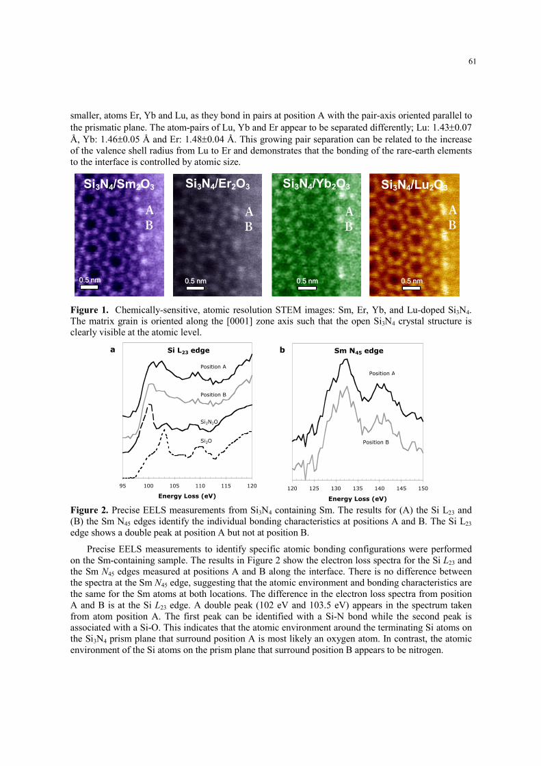
As an example of the use of the FEI Tecnai F20 in the high spatial resolution mode here we discuss results from the analysis of grain boundaries in Si3N4 Bulk Si3N4 ceramics are currently limited by a brittleness that reduces their reliability Such properties can be improved by the incorporation of an intergranular phase An understanding of how this phase governs the macroscopic mechanical properties has been limited because the amorphous morphology of the phase and its small dimension makes analysis difficult However the ability of the scanning transmission electron microscope to probe the interface structure offers the potential to understand the atomic scale phenomena occurring in these materials Figure 1 shows the interface between the intergranular phase and a Si3N4 matrix grain for each of four sintering additive types Sm2O3 Er2O3 Yb2O3 and Lu2O3 [9] The bright spots that appear at the interface in the amorphous intergranular phase are attributed to columns of Sm Er Yb and Lu atoms respectively These images clearly show that the atomic bonding of those atoms along the Si3N4 prismatic plane is periodic and occurs at very specific atomic sites Sm atoms bond in single-atom configuration to both positions A and B This changes with the slightly heavier but
60
smaller atoms Er Yb and Lu as they bond in pairs at position A with the pair-axis oriented parallel to the prismatic plane The atom-pairs of Lu Yb and Er appear to be separated differently Lu 143plusmn007 Aring Yb 146plusmn005 Aring and Er 148plusmn004 Aring This growing pair separation can be related to the increase of the valence shell radius from Lu to Er and demonstrates that the bonding of the rare-earth elements to the interface is controlled by atomic size
Figure 1 Chemically-sensitive atomic resolution STEM images Sm Er Yb and Lu-doped Si3N4 The matrix grain is oriented along the [0001] zone axis such that the open Si3N4 crystal structure is clearly visible at the atomic level
Figure 2 Precise EELS measurements from Si3N4 containing Sm The results for (A) the Si L23 and (B) the Sm N45 edges identify the individual bonding characteristics at positions A and B The Si L23 edge shows a double peak at position A but not at position B
Precise EELS measurements to identify specific atomic bonding configurations were performed on the Sm-containing sample The results in Figure 2 show the electron loss spectra for the Si L23 and the Sm N45 edges measured at positions A and B along the interface There is no difference between the spectra at the Sm N45 edge suggesting that the atomic environment and bonding characteristics are the same for the Sm atoms at both locations The difference in the electron loss spectra from position A and B is at the Si L23 edge A double peak (102 eV and 1035 eV) appears in the spectrum taken from atom position A The first peak can be identified with a Si-N bond while the second peak is associated with a Si-O This indicates that the atomic environment around the terminating Si atoms on the Si3N4 prism plane that surround position A is most likely an oxygen atom In contrast the atomic environment of the Si atoms on the prism plane that surround position B appears to be nitrogen
Si3N4Sm2O3 Si3N4Er2O3 Si3N4Yb2O3 Si3N4Lu2O3
0055 nnmm 0055 nnmm 0055 nnmm 0055 nnmm
95 100 105 110 115 120
Energy Loss (eV)
Position A
Position B
Si2N2O
Si2O
Si L23 edgea
120 125 130 135 140 145 150
Energy Loss (eV)
Position A
Position B
Sm N45 edgeb
A
B AB
AB
AB
61
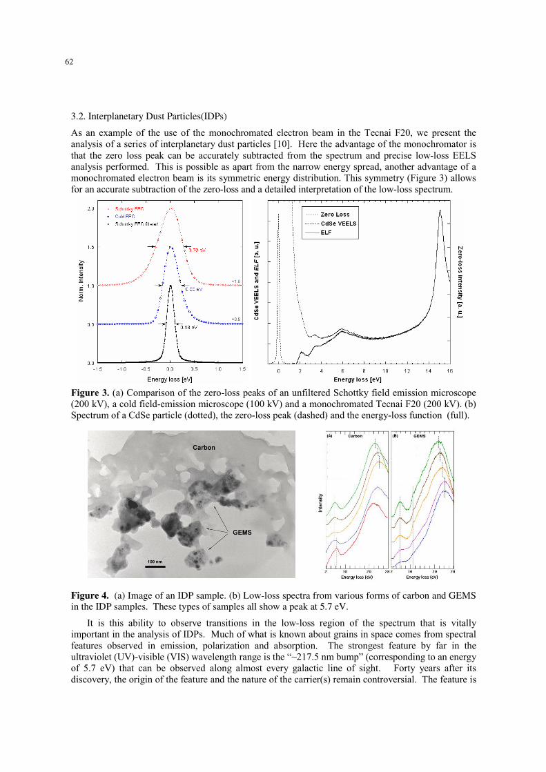
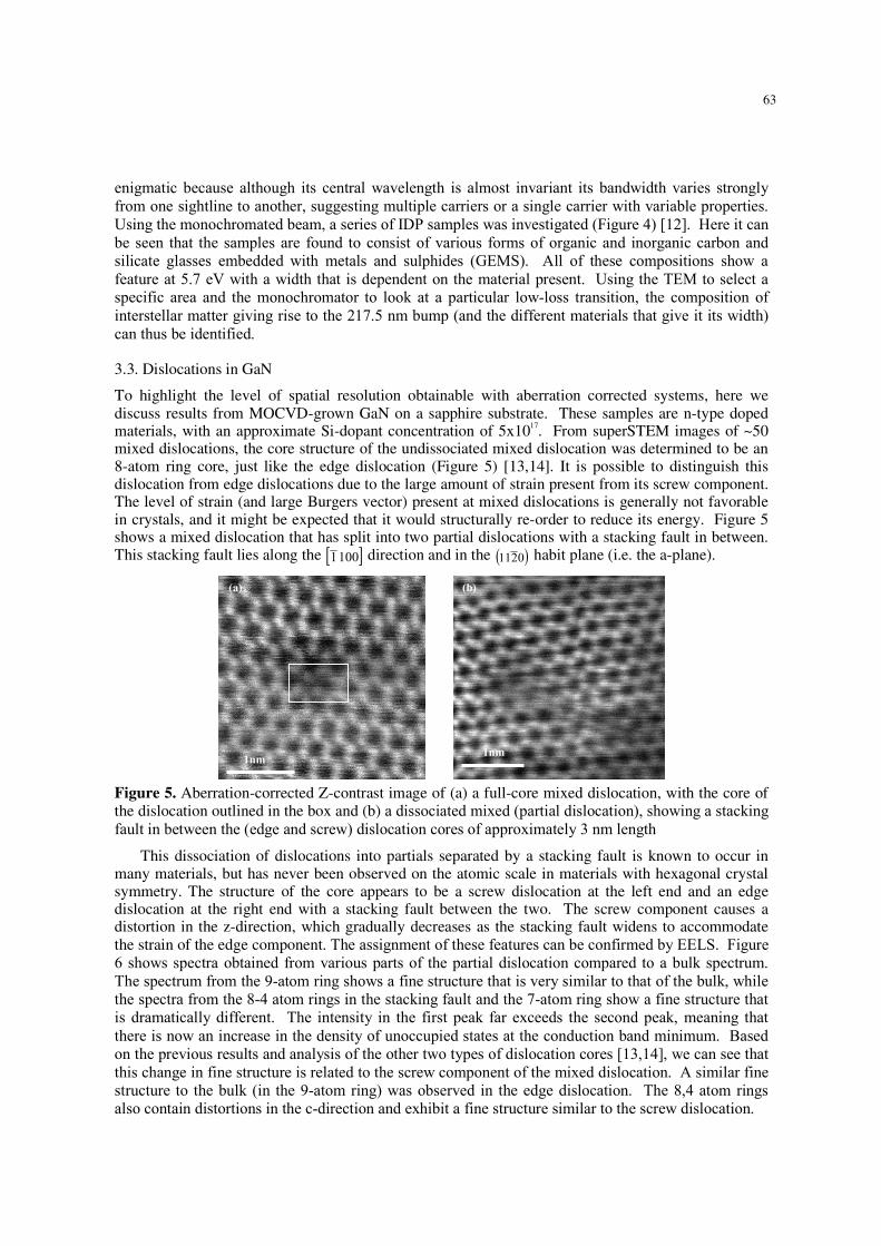
32 Interplanetary Dust Particles(IDPs)
As an example of the use of the monochromated electron beam in the Tecnai F20 we present the analysis of a series of interplanetary dust particles [10] Here the advantage of the monochromator is that the zero loss peak can be accurately subtracted from the spectrum and precise low-loss EELS analysis performed This is possible as apart from the narrow energy spread another advantage of a monochromated electron beam is its symmetric energy distribution This symmetry (Figure 3) allows for an accurate subtraction of the zero-loss and a detailed interpretation of the low-loss spectrum
Figure 3 (a) Comparison of the zero-loss peaks of an unfiltered Schottky field emission microscope (200 kV) a cold field-emission microscope (100 kV) and a monochromated Tecnai F20 (200 kV) (b) Spectrum of a CdSe particle (dotted) the zero-loss peak (dashed) and the energy-loss function (full)
Figure 4 (a) Image of an IDP sample (b) Low-loss spectra from various forms of carbon and GEMS in the IDP samples These types of samples all show a peak at 57 eV
It is this ability to observe transitions in the low-loss region of the spectrum that is vitally important in the analysis of IDPs Much of what is known about grains in space comes from spectral features observed in emission polarization and absorption The strongest feature by far in the ultraviolet (UV)-visible (VIS) wavelength range is the ldquo~2175 nm bumprdquo (corresponding to an energy of 57 eV) that can be observed along almost every galactic line of sight Forty years after its discovery the origin of the feature and the nature of the carrier(s) remain controversial The feature is
62
enigmatic because although its central wavelength is almost invariant its bandwidth varies strongly from one sightline to another suggesting multiple carriers or a single carrier with variable properties Using the monochromated beam a series of IDP samples was investigated (Figure 4) [12] Here it can be seen that the samples are found to consist of various forms of organic and inorganic carbon and silicate glasses embedded with metals and sulphides (GEMS) All of these compositions show a feature at 57 eV with a width that is dependent on the material present Using the TEM to select a specific area and the monochromator to look at a particular low-loss transition the composition of interstellar matter giving rise to the 2175 nm bump (and the different materials that give it its width) can thus be identified
33 Dislocations in GaN
To highlight the level of spatial resolution obtainable with aberration corrected systems here we discuss results from MOCVD-grown GaN on a sapphire substrate These samples are n-type doped materials with an approximate Si-dopant concentration of 5x10¹⁷ From superSTEM images of ~50 mixed dislocations the core structure of the undissociated mixed dislocation was determined to be an 8-atom ring core just like the edge dislocation (Figure 5) [1314] It is possible to distinguish this dislocation from edge dislocations due to the large amount of strain present from its screw component The level of strain (and large Burgers vector) present at mixed dislocations is generally not favorable in crystals and it might be expected that it would structurally re-order to reduce its energy Figure 5 shows a mixed dislocation that has split into two partial dislocations with a stacking fault in between This stacking fault lies along the [ ]1001 direction and in the ( )0211 habit plane (ie the a-plane)
Figure 5 Aberration-corrected Z-contrast image of (a) a full-core mixed dislocation with the core of the dislocation outlined in the box and (b) a dissociated mixed (partial dislocation) showing a stacking fault in between the (edge and screw) dislocation cores of approximately 3 nm length
This dissociation of dislocations into partials separated by a stacking fault is known to occur in many materials but has never been observed on the atomic scale in materials with hexagonal crystal symmetry The structure of the core appears to be a screw dislocation at the left end and an edge dislocation at the right end with a stacking fault between the two The screw component causes a distortion in the z-direction which gradually decreases as the stacking fault widens to accommodate the strain of the edge component The assignment of these features can be confirmed by EELS Figure 6 shows spectra obtained from various parts of the partial dislocation compared to a bulk spectrum The spectrum from the 9-atom ring shows a fine structure that is very similar to that of the bulk while the spectra from the 8-4 atom rings in the stacking fault and the 7-atom ring show a fine structure that is dramatically different The intensity in the first peak far exceeds the second peak meaning that there is now an increase in the density of unoccupied states at the conduction band minimum Based on the previous results and analysis of the other two types of dislocation cores [1314] we can see that this change in fine structure is related to the screw component of the mixed dislocation A similar fine structure to the bulk (in the 9-atom ring) was observed in the edge dislocation The 84 atom rings also contain distortions in the c-direction and exhibit a fine structure similar to the screw dislocation
1nm
(a) (b)
1nm
63
Figure 6 (a) schematic of the dissociated dislocation (b) spectra taken from points around the core
4 Conclusions
Monochromators and aberration correctors have significantly increased the sensitivity of energy loss spectroscopy its applicability to the low-loss spectroscopy and its spatial resolution for core-loss spectroscopy When monochromators and aberration correctors are incorporated into the same instrument in the future spatial resolution of 01 nm and energy resolution of 01 eV can be expected
Acknowledgements
Aspects of this work were performed in collaboration with C F Kisielowski R O Ritchie and M K Cinibulk Work performed at the National Center for Electron Microscopy Lawrence Berkeley National Laboratory was supported by the Director Office of Science of the US Department of Energy (DoE) under Contract No DE-AC03-76SF00098 and by grant No DE-FG02-03ER46057
References
[1] Browning N D Chisholm M F and Pennycook S J 1993 Nature 366 143-146 [2] Batson P E 1993 Nature 366 727-728 [3] Muller D A Tzou Y Ray R and Silcox J 1993 Nature 366 725-727 [4] Egerton R F 1996 Electron Energy Loss Spectroscopy in the Electron Microscope (Plenum) [5] Erni R and Browning N D in press Ultramicroscopy [6] Erni R and Browning N D submitted Applied Physics Letters [7] Erni R Browning N D Dai Z and Bradley J P 2005 Micron 36 369-379 [8] Browning N D Erni R Lopatin S Ziegler A Idrobo J C Kisielowski C F Cinibulk M K and
Ritchie R O 2005 FEI Applied Solutions 1 16-27 [9] Ziegler A Idrobo J C Cinibulk M K Kisielowski C F Browning N D and Ritchie R O 2004
Science 306 1768-1770 [10] Bradley J P Dai Z Erni R Browning N D Graham G Weber P Smith J Hutcheon I Ishii H
Bajt S Floss C and Stadermann F 2005 Science 307 244-247 [11] Klie R F Buban J P Varela M Franceschetti A Joos C Zhu Y Browning N D Pantelides S T
and Pennycook S J 2005 Nature435 475-478 [12] Arslan I Bleloch A Stach E A and Browning N D 2005 Physical Review Letters 94 025504 [13] Arslan I and Browning N D 2003 Physical Review Letters 91 165501 [14] Arslan I and Browning N D 2002 Physical Review B 65 075310
1
0
400
800
1200
1600
2000
2400
2800
3200
400 410 420 430 440 450
Energy (eV)
Bulk
7-atom ring
8-4 atom rings
9-atom ring
64
Monochromators and Aberration Correctors Taking EELS to New Levels of Energy and Spatial Resolution
N D Browning12 I Arslan3 R Erni2 J C Idrobo2 A Ziegler24 J Bradley4 Z Dai4
E A Stach5 A Bleloch6
1National Center for Electron Microscopy MS 72-150 Lawrence Berkeley National Laboratory Berkeley CA 94720 USA 2Department of Chemical Engineering and Materials Science University of California-Davis 1 Shields Ave Davis Ca 95616 USA 3Department of Materials Science and Metallurgy University of Cambridge Pembroke Street Cambridge CB2 3QZ UK 4Lawrence Livermore National Laboratory Institute for Geophysics and Planetary Physics 7000 East Avenue Livermore CA 94551 USA 5School of Materials Engineering Purdue University West Lafayette IN 47907 USA 6UK SuperSTEM Daresbury Laboratory Daresbury Cheshire WA4 4AD UK
nbrowningucdavisedu
Abstract The development of monochromators and aberration correctors for transmission electron microscopes (TEM) has paved the way for a level of imaging and analysis that is unmatched by other methods While current instrumentation does not permit the optimum spatial resolution of the microscope to be coupled with this high energy resolution detailed spectroscopic analyses can be performed with ~1nm spatial resolution Combined with ~01 eV energy resolution this is particularly useful for the analysis of the low-loss region of the spectrum permitting quantum confinement effects and optical responses of individual nanostructures to be measured Higher spatial resolution can be obtained from aberration corrected STEM where spectral resolution of ~04eV can be coupled with a spatial resolution of lt01 nm Such resolution is particularly useful for analyzing core-loss signals at defects and interfaces where localized structural and compositional modulations are expected to have a large effect on the structure-property relationships Results from aberration corrected and monochromated systems will be presented to highlight the application of EELS to the study of Si3N4 GaN and extraterrestrial particles
1 Introduction
The ability to use Z-contrast images in the scanning transmission electron microscope (STEM) to position the electron beam for electron energy loss spectroscopy (EELS) provides a powerful tool to characterize individual nanostructures defects and interfaces [1-3] Knowledge of the exact location of the beam (to ~01 nm precision) enables the local electronic structure to be correlated precisely with the atomic structure and composition of the feature being investigated Although EELS has been used
Institute of Physics Publishing Journal of Physics Conference Series 26 (2006) 59ndash64doi1010881742-6596261014 EMAGndashNANO 05 Imaging Analysis and Fabrication on the Nanoscale
59copy 2006 IOP Publishing Ltd
for decades to investigate the local electronic properties of materials [see for example 4] the recent development of monochromators and aberration correctors has significantly extended both the sensitivity of the method and its spatial resolution In this paper recent results from both monochromated and aberration corrected instruments will be presented that highlight the increases in sensitivity and resolution that have been achieved
2 Instrumentation
21 Monochromated Schottky Field Emission FEI Tecnai F20
The results described here were obtained on the FEI monochromated Tecnai F20 operating at 200kV [5-8] in the National Center for Electron Microscopy (NCEM) at Lawrence Berkeley National Laboratory (LBNL) Spectra are recorded on a post-column Gatan electron energy-loss spectrometer with an insertable annular detector being used for STEM imaging For the Tecnai F20 at NCEM an electron probe of 014 nm in diameter has been demonstrated [9] In this high spatial resolution mode with the monochromator off an energy resolution of 05 eV is achieved The current system does not achieve such small probes when the monochromator is on (~05 to 1 nm probes have been achieved [10]) The reason is that the position of the virtual source does not allow the condenser lens system to achieve the level of demagnification necessary for the smallest probe However as the main benefit of the monochromator is for low-loss EELS this is not a major limitation as the spatial resolution of EELS at energy losses below ~20 eV is hardly affected by the actual size of the probe [5]
22 Nion Aberration Corrected Cold Field Emission VG HB501
The ability to obtain high spatial resolution EELS (lt01nm) has arisen through aberration correction of a VG dedicated STEM [11] The high spatial resolution studies in this paper [12] were performed at the UK superSTEM laboratory on a VG HB501 dedicated STEM fitted with a 2nd generation spherical aberration corrector a spectroscopy coupling module (both manufactured by Nion Co) and a Gatan Enfina electron energy loss spectrometer The spectroscopy-coupling module is necessary to compress the angular range of the bright field disk (which is large due to the convergence angle required for the 01 nm resolution) so that the 2mm entrance aperture to the spectrometer can collect a reasonable fraction of the electrons that pass through the sample while maintaining 04 eV spectral resolution Particular care was taken with the environment resulting in a spatial resolution of 01 nm with about 60 pA probe current and a drift stability of 005nm in 100s The convergence semi-angle of the electron probe was 24 mrad for both imaging and spectroscopy The collection semi-angle for the EELS spectra was 15 mrad and for the Z-contrast imaging was 70 to 200 mrad
3 Results
31 Si3N
4 Grain Boundaries
As an example of the use of the FEI Tecnai F20 in the high spatial resolution mode here we discuss results from the analysis of grain boundaries in Si3N4 Bulk Si3N4 ceramics are currently limited by a brittleness that reduces their reliability Such properties can be improved by the incorporation of an intergranular phase An understanding of how this phase governs the macroscopic mechanical properties has been limited because the amorphous morphology of the phase and its small dimension makes analysis difficult However the ability of the scanning transmission electron microscope to probe the interface structure offers the potential to understand the atomic scale phenomena occurring in these materials Figure 1 shows the interface between the intergranular phase and a Si3N4 matrix grain for each of four sintering additive types Sm2O3 Er2O3 Yb2O3 and Lu2O3 [9] The bright spots that appear at the interface in the amorphous intergranular phase are attributed to columns of Sm Er Yb and Lu atoms respectively These images clearly show that the atomic bonding of those atoms along the Si3N4 prismatic plane is periodic and occurs at very specific atomic sites Sm atoms bond in single-atom configuration to both positions A and B This changes with the slightly heavier but
60
smaller atoms Er Yb and Lu as they bond in pairs at position A with the pair-axis oriented parallel to the prismatic plane The atom-pairs of Lu Yb and Er appear to be separated differently Lu 143plusmn007 Aring Yb 146plusmn005 Aring and Er 148plusmn004 Aring This growing pair separation can be related to the increase of the valence shell radius from Lu to Er and demonstrates that the bonding of the rare-earth elements to the interface is controlled by atomic size
Figure 1 Chemically-sensitive atomic resolution STEM images Sm Er Yb and Lu-doped Si3N4 The matrix grain is oriented along the [0001] zone axis such that the open Si3N4 crystal structure is clearly visible at the atomic level
Figure 2 Precise EELS measurements from Si3N4 containing Sm The results for (A) the Si L23 and (B) the Sm N45 edges identify the individual bonding characteristics at positions A and B The Si L23 edge shows a double peak at position A but not at position B
Precise EELS measurements to identify specific atomic bonding configurations were performed on the Sm-containing sample The results in Figure 2 show the electron loss spectra for the Si L23 and the Sm N45 edges measured at positions A and B along the interface There is no difference between the spectra at the Sm N45 edge suggesting that the atomic environment and bonding characteristics are the same for the Sm atoms at both locations The difference in the electron loss spectra from position A and B is at the Si L23 edge A double peak (102 eV and 1035 eV) appears in the spectrum taken from atom position A The first peak can be identified with a Si-N bond while the second peak is associated with a Si-O This indicates that the atomic environment around the terminating Si atoms on the Si3N4 prism plane that surround position A is most likely an oxygen atom In contrast the atomic environment of the Si atoms on the prism plane that surround position B appears to be nitrogen
Si3N4Sm2O3 Si3N4Er2O3 Si3N4Yb2O3 Si3N4Lu2O3
0055 nnmm 0055 nnmm 0055 nnmm 0055 nnmm
95 100 105 110 115 120
Energy Loss (eV)
Position A
Position B
Si2N2O
Si2O
Si L23 edgea
120 125 130 135 140 145 150
Energy Loss (eV)
Position A
Position B
Sm N45 edgeb
A
B AB
AB
AB
61
32 Interplanetary Dust Particles(IDPs)
As an example of the use of the monochromated electron beam in the Tecnai F20 we present the analysis of a series of interplanetary dust particles [10] Here the advantage of the monochromator is that the zero loss peak can be accurately subtracted from the spectrum and precise low-loss EELS analysis performed This is possible as apart from the narrow energy spread another advantage of a monochromated electron beam is its symmetric energy distribution This symmetry (Figure 3) allows for an accurate subtraction of the zero-loss and a detailed interpretation of the low-loss spectrum
Figure 3 (a) Comparison of the zero-loss peaks of an unfiltered Schottky field emission microscope (200 kV) a cold field-emission microscope (100 kV) and a monochromated Tecnai F20 (200 kV) (b) Spectrum of a CdSe particle (dotted) the zero-loss peak (dashed) and the energy-loss function (full)
Figure 4 (a) Image of an IDP sample (b) Low-loss spectra from various forms of carbon and GEMS in the IDP samples These types of samples all show a peak at 57 eV
It is this ability to observe transitions in the low-loss region of the spectrum that is vitally important in the analysis of IDPs Much of what is known about grains in space comes from spectral features observed in emission polarization and absorption The strongest feature by far in the ultraviolet (UV)-visible (VIS) wavelength range is the ldquo~2175 nm bumprdquo (corresponding to an energy of 57 eV) that can be observed along almost every galactic line of sight Forty years after its discovery the origin of the feature and the nature of the carrier(s) remain controversial The feature is
62
enigmatic because although its central wavelength is almost invariant its bandwidth varies strongly from one sightline to another suggesting multiple carriers or a single carrier with variable properties Using the monochromated beam a series of IDP samples was investigated (Figure 4) [12] Here it can be seen that the samples are found to consist of various forms of organic and inorganic carbon and silicate glasses embedded with metals and sulphides (GEMS) All of these compositions show a feature at 57 eV with a width that is dependent on the material present Using the TEM to select a specific area and the monochromator to look at a particular low-loss transition the composition of interstellar matter giving rise to the 2175 nm bump (and the different materials that give it its width) can thus be identified
33 Dislocations in GaN
To highlight the level of spatial resolution obtainable with aberration corrected systems here we discuss results from MOCVD-grown GaN on a sapphire substrate These samples are n-type doped materials with an approximate Si-dopant concentration of 5x10¹⁷ From superSTEM images of ~50 mixed dislocations the core structure of the undissociated mixed dislocation was determined to be an 8-atom ring core just like the edge dislocation (Figure 5) [1314] It is possible to distinguish this dislocation from edge dislocations due to the large amount of strain present from its screw component The level of strain (and large Burgers vector) present at mixed dislocations is generally not favorable in crystals and it might be expected that it would structurally re-order to reduce its energy Figure 5 shows a mixed dislocation that has split into two partial dislocations with a stacking fault in between This stacking fault lies along the [ ]1001 direction and in the ( )0211 habit plane (ie the a-plane)
Figure 5 Aberration-corrected Z-contrast image of (a) a full-core mixed dislocation with the core of the dislocation outlined in the box and (b) a dissociated mixed (partial dislocation) showing a stacking fault in between the (edge and screw) dislocation cores of approximately 3 nm length
This dissociation of dislocations into partials separated by a stacking fault is known to occur in many materials but has never been observed on the atomic scale in materials with hexagonal crystal symmetry The structure of the core appears to be a screw dislocation at the left end and an edge dislocation at the right end with a stacking fault between the two The screw component causes a distortion in the z-direction which gradually decreases as the stacking fault widens to accommodate the strain of the edge component The assignment of these features can be confirmed by EELS Figure 6 shows spectra obtained from various parts of the partial dislocation compared to a bulk spectrum The spectrum from the 9-atom ring shows a fine structure that is very similar to that of the bulk while the spectra from the 8-4 atom rings in the stacking fault and the 7-atom ring show a fine structure that is dramatically different The intensity in the first peak far exceeds the second peak meaning that there is now an increase in the density of unoccupied states at the conduction band minimum Based on the previous results and analysis of the other two types of dislocation cores [1314] we can see that this change in fine structure is related to the screw component of the mixed dislocation A similar fine structure to the bulk (in the 9-atom ring) was observed in the edge dislocation The 84 atom rings also contain distortions in the c-direction and exhibit a fine structure similar to the screw dislocation
1nm
(a) (b)
1nm
63
Figure 6 (a) schematic of the dissociated dislocation (b) spectra taken from points around the core
4 Conclusions
Monochromators and aberration correctors have significantly increased the sensitivity of energy loss spectroscopy its applicability to the low-loss spectroscopy and its spatial resolution for core-loss spectroscopy When monochromators and aberration correctors are incorporated into the same instrument in the future spatial resolution of 01 nm and energy resolution of 01 eV can be expected
Acknowledgements
Aspects of this work were performed in collaboration with C F Kisielowski R O Ritchie and M K Cinibulk Work performed at the National Center for Electron Microscopy Lawrence Berkeley National Laboratory was supported by the Director Office of Science of the US Department of Energy (DoE) under Contract No DE-AC03-76SF00098 and by grant No DE-FG02-03ER46057
References
[1] Browning N D Chisholm M F and Pennycook S J 1993 Nature 366 143-146 [2] Batson P E 1993 Nature 366 727-728 [3] Muller D A Tzou Y Ray R and Silcox J 1993 Nature 366 725-727 [4] Egerton R F 1996 Electron Energy Loss Spectroscopy in the Electron Microscope (Plenum) [5] Erni R and Browning N D in press Ultramicroscopy [6] Erni R and Browning N D submitted Applied Physics Letters [7] Erni R Browning N D Dai Z and Bradley J P 2005 Micron 36 369-379 [8] Browning N D Erni R Lopatin S Ziegler A Idrobo J C Kisielowski C F Cinibulk M K and
Ritchie R O 2005 FEI Applied Solutions 1 16-27 [9] Ziegler A Idrobo J C Cinibulk M K Kisielowski C F Browning N D and Ritchie R O 2004
Science 306 1768-1770 [10] Bradley J P Dai Z Erni R Browning N D Graham G Weber P Smith J Hutcheon I Ishii H
Bajt S Floss C and Stadermann F 2005 Science 307 244-247 [11] Klie R F Buban J P Varela M Franceschetti A Joos C Zhu Y Browning N D Pantelides S T
and Pennycook S J 2005 Nature435 475-478 [12] Arslan I Bleloch A Stach E A and Browning N D 2005 Physical Review Letters 94 025504 [13] Arslan I and Browning N D 2003 Physical Review Letters 91 165501 [14] Arslan I and Browning N D 2002 Physical Review B 65 075310
1
0
400
800
1200
1600
2000
2400
2800
3200
400 410 420 430 440 450
Energy (eV)
Bulk
7-atom ring
8-4 atom rings
9-atom ring
64
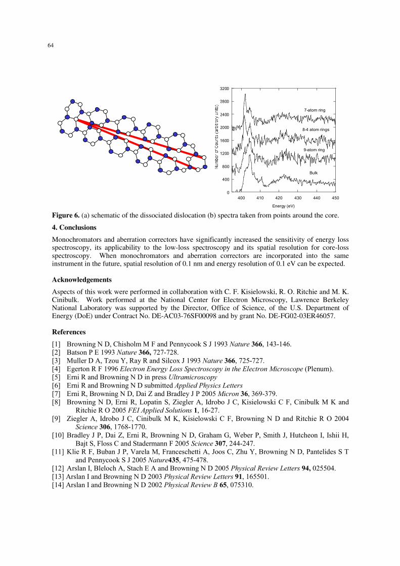