
Molecular Lithography through DNA-Mediated Etching … · 1 Molecular Lithography through...
4
1 Molecular Lithography through DNA-Mediated Etching and 2 Masking of SiO 2 3 Sumedh P. Surwade, †,§ Shichao Zhao, †,‡,§ and Haitao Liu* ,† 4 † Department of Chemistry, University of Pittsburgh, Pittsburgh, Pennsylvania 15260, United States 5 ‡ College of Materials & Environmental Engineering, Hangzhou Dianzi University, Hangzhou 310018, P. R. China 6 b S Supporting Information 7 ABSTRACT: We demonstrate a new approach to pattern 8 transfer for bottom-up nanofabrication. We show that DNA 9 promotes/inhibits the etching of SiO 2 at the single-molecule 10 level, resulting in negative/positive tone pattern transfers from DNA to the SiO 2 substrate. 12 13 S tate-of-the-art photolithography processes use 193 nm light 14 to produce diffraction-limited features as small as 32 nm. 1 15 The use of even shorter wavelengths of light faces significant 16 technological and economic challenges because of the cost and 17 complexity of the exposure optics and the high-energy light 18 source. Thus, over the past few years, significant efforts have been 19 dedicated toward alternative lithography processes that can 20 produce features with sizes in the range of tens of nanometers. 21 In recent years, self-assembly of DNA, especially of scaffolded 22 DNA origami, has matured to a stage where arbitrary two- and 23 three-dimensional shapes with controlled dimensions at the 24 nanoscale can easily be constructed. 2,3 These DNA nanostruc- 25 tures have been used to direct the assembly of nanoparticles, 26 carbon nanotubes, and biological molecules. 415 With a pat- 27 terned substrate, they can be deposited with precise control 28 over their location and orientation, opening up the possibility 29 that they can be fully integrated with conventional lithography 30 processes. 5,14,16,17 31 In view of the degree of control over their sizes and shapes, 32 these DNA nanostructures should be ideal templates for bottom- 33 up nanofabrication. Unfortunately, DNA nanostructures have 34 limited chemical stability and poor adhesion to common inor- 35 ganic substrates, both of which make it difficult to transfer their 36 shape to the substrate. Traditional pattern transfer processes are 37 based on the concept of masking, in which the mask protects the 38 substrate from reacting with the harsh etchant. This approach 39 requires that the mask be chemically and mechanically stable 40 during the etching reaction. Molecular-scale templates such as 41 DNA nanostructures are inherently incompatible with this pattern 42 transfer approach. For example, two of the most often used 43 methods to etch silicon oxide (SiO 2 ) are dry etching using plasma 44 and wet etching using buffered HF solution. The plasma would 45 instantly destroy the DNA, while the buffered HF solution would 46 immediately lift the DNA off the substrate. Indeed, while DNA 47 nanostructures have been used as templates for nanofabri- 48 cation, 18,19 these processes have inevitably used an evaporated 49 metal film as the intermediate etching mask. A one-step pattern 50 transfer from DNA to an inorganic substrate has not been reported. 51 Herein we propose a new approach to pattern transfer in 52 which the DNA modulates the vapor-phase etching of SiO 2 at the 53 single-molecule level, resulting in a direct pattern transfer from 54 DNA to SiO 2 . 55 Vapor-phase etching has been known to produce selective, 56 reproducible, and uniform etching of various inorganic sub- 57 strates. Relative to the wet-etching and plasma-etching processes, 58 it offers much more versatility in the range of process variables, 20,21 59 and most important of all, vapor-phase etching can be carried out 60 under very mild conditions that will not lift off or destroy the 61 DNA-based templates. 62 The vapor-phase etching of SiO 2 using HF gas is characterized 63 by the thermodynamically favorable reaction between SiO 2 and 64 HF gas to produce SiF 4 and H 2 O: 21 SiO 2 ðsÞþ 4HFðgÞ f SiF 4 ðgÞþ 2H 2 OðgÞ 65 However, to overcome the kinetic barrier, water is needed as a 66 catalyst in the reaction, since HF alone does not etch SiO 2 . 67 Experimental evidence based on in situ FTIR spectroscopy has 68 suggested that HF and H 2 O molecules form a HFH 2 O 69 complex that adsorbs on the SiO 2 surface more strongly than 70 either molecule alone. 21,22 Other mechanistic studies 21 have 71 suggested that the etching reaction starts with the deprotonation 72 of HF by water to generate HF 2 ions: 6HF þ 3H 2 O f 3HF 2 þ 3H 3 O þ 73 These ions then etch away SiO 2 to produce water and other 74 gaseous products: 3HF 2 þ 3H 3 O þ þ SiO 2 f 2HF þ SiF 4 þ 5H 2 O 75 The reaction is usually initiated by the trace amount of surface- 76 adsorbed water on the oxide substrate. Notably, more water 77 (5 equiv) is produced in the etching step than initially consumed 78 (3 equiv) in the deprotonation step. As the reaction progresses, 79 both the surface water concentration and the reaction rate 80 increase; the overall reaction is autocatalytic. 81 All of this information suggests that the etching rate of SiO 2 is 82 positively correlated with the concentration of surface-adsorbed 83 water. We hypothesized that if the adsorption of water on the 84 SiO 2 surface could be controlled with nanometer-scale resolu- 85 tion, it would be possible to modulate the etching of SiO 2 at the 86 same length scale. The spatial variation in the concentration of 87 surface-adsorbed water would not need to be very high: since the 88 etching reaction is autocatalytic, small variations in the initial Received: April 27, 2011 Journal of the American Chemical Society | 3b2 | ver.9 | 14/7/011 | 8:23 | Msc: ja-2011-038886 | TEID: rdk00 | BATID: 00000 | Pages: 3.25 COMMUNICATION pubs.acs.org/JACS rXXXX American Chemical Society A dx.doi.org/10.1021/ja2038886 | J. Am. Chem. Soc. XXXX, XXX, 000–000
Transcript of Molecular Lithography through DNA-Mediated Etching … · 1 Molecular Lithography through...

1 Molecular Lithography through DNA-Mediated Etching and2 Masking of SiO2
3 Sumedh P. Surwade,†,§ Shichao Zhao,†,‡,§ and Haitao Liu*,†
4†Department of Chemistry, University of Pittsburgh, Pittsburgh, Pennsylvania 15260, United States
5‡College of Materials & Environmental Engineering, Hangzhou Dianzi University, Hangzhou 310018, P. R. China
6 bS Supporting Information
7 ABSTRACT: We demonstrate a new approach to pattern8 transfer for bottom-up nanofabrication. We show that DNA9 promotes/inhibits the etching of SiO2 at the single-molecule10 level, resulting in negative/positive tone pattern transfers
11
from DNA to the SiO2 substrate.12
13 State-of-the-art photolithography processes use 193 nm light14 to produce diffraction-limited features as small as 32 nm.1
15 The use of even shorter wavelengths of light faces significant16 technological and economic challenges because of the cost and17 complexity of the exposure optics and the high-energy light18 source. Thus, over the past few years, significant efforts have been19 dedicated toward alternative lithography processes that can20 produce features with sizes in the range of tens of nanometers.21 In recent years, self-assembly of DNA, especially of scaffolded22 DNA origami, has matured to a stage where arbitrary two- and23 three-dimensional shapes with controlled dimensions at the24 nanoscale can easily be constructed.2,3 These DNA nanostruc-25 tures have been used to direct the assembly of nanoparticles,26 carbon nanotubes, and biological molecules.4�15 With a pat-27 terned substrate, they can be deposited with precise control28 over their location and orientation, opening up the possibility29 that they can be fully integrated with conventional lithography30 processes.5,14,16,17
31 In view of the degree of control over their sizes and shapes,32 these DNA nanostructures should be ideal templates for bottom-33 up nanofabrication. Unfortunately, DNA nanostructures have34 limited chemical stability and poor adhesion to common inor-35 ganic substrates, both of which make it difficult to transfer their36 shape to the substrate. Traditional pattern transfer processes are37 based on the concept of masking, in which the mask protects the38 substrate from reacting with the harsh etchant. This approach39 requires that the mask be chemically and mechanically stable40 during the etching reaction. Molecular-scale templates such as41 DNA nanostructures are inherently incompatible with this pattern42 transfer approach. For example, two of the most often used43 methods to etch silicon oxide (SiO2) are dry etching using plasma44 and wet etching using buffered HF solution. The plasma would45 instantly destroy the DNA, while the buffered HF solution would46 immediately lift the DNA off the substrate. Indeed, while DNA47 nanostructures have been used as templates for nanofabri-48 cation,18,19 these processes have inevitably used an evaporated49 metal film as the intermediate etching mask. A one-step pattern50 transfer fromDNA to an inorganic substrate has not been reported.
51Herein we propose a new approach to pattern transfer in52which the DNAmodulates the vapor-phase etching of SiO2 at the53single-molecule level, resulting in a direct pattern transfer from54DNA to SiO2.55Vapor-phase etching has been known to produce selective,56reproducible, and uniform etching of various inorganic sub-57strates. Relative to the wet-etching and plasma-etching processes,58it offers much more versatility in the range of process variables,20,21
59and most important of all, vapor-phase etching can be carried out60under very mild conditions that will not lift off or destroy the61DNA-based templates.62The vapor-phase etching of SiO2 using HF gas is characterized63by the thermodynamically favorable reaction between SiO2 and64HF gas to produce SiF4 and H2O:
21
SiO2ðsÞ þ 4HFðgÞ f SiF4ðgÞ þ 2H2OðgÞ65However, to overcome the kinetic barrier, water is needed as a66catalyst in the reaction, since HF alone does not etch SiO2.67Experimental evidence based on in situ FTIR spectroscopy has68suggested that HF and H2O molecules form a HF�H2O69complex that adsorbs on the SiO2 surface more strongly than70either molecule alone.21,22 Other mechanistic studies21 have71suggested that the etching reaction starts with the deprotonation72of HF by water to generate HF2
� ions:
6HF þ 3H2O f 3HF2� þ 3H3O
þ
73These ions then etch away SiO2 to produce water and other74gaseous products:
3HF2� þ 3H3O
þ þ SiO2 f 2HF þ SiF4 þ 5H2O
75The reaction is usually initiated by the trace amount of surface-76adsorbed water on the oxide substrate. Notably, more water77(5 equiv) is produced in the etching step than initially consumed78(3 equiv) in the deprotonation step. As the reaction progresses,79both the surface water concentration and the reaction rate80increase; the overall reaction is autocatalytic.81All of this information suggests that the etching rate of SiO2 is82positively correlated with the concentration of surface-adsorbed83water. We hypothesized that if the adsorption of water on the84SiO2 surface could be controlled with nanometer-scale resolu-85tion, it would be possible to modulate the etching of SiO2 at the86same length scale. The spatial variation in the concentration of87surface-adsorbed water would not need to be very high: since the88etching reaction is autocatalytic, small variations in the initial
Received: April 27, 2011
Journal of the American Chemical Society | 3b2 | ver.9 | 14/7/011 | 8:23 | Msc: ja-2011-038886 | TEID: rdk00 | BATID: 00000 | Pages: 3.25
COMMUNICATION
pubs.acs.org/JACS
rXXXX American Chemical Society A dx.doi.org/10.1021/ja2038886 | J. Am. Chem. Soc. XXXX, XXX, 000–000
89 water concentration would be amplified by the reaction and90 could have a significant impact on the etching kinetics in the91 long run.92 To verify this hypothesis experimentally, we used DNA93 nanostructures as templates for spatial modulation of the adsorp-94 tion of water on a SiO2 surface. DNA molecules contain phos-95 phate groups as well as nitrogen and oxygen atoms that can96 hydrogen bondwith water.23When aDNAmolecule is deposited97 onto a SiO2 surface, its presence undoubtedly affects the water98 adsorption around it. Since the SiO2 surface also absorbs water by99 itself, the difference between the concentrations of surface-100 absorbed water on the clean SiO2 surface and the SiO2 under101 DNA depends on, amongmany other factors, the relative humidity102 of the environment and the temperature of the substrate. Though103 we cannot predict the exact spatial profile of the water concen-104 tration, we expect the DNA molecule to provide local modula-105 tion of the etching rate of SiO2, producing nanoscale patterns106 that duplicate its shape.107 There are twomajor differences between the water adsorption108 isotherms on DNA23 and on SiO2
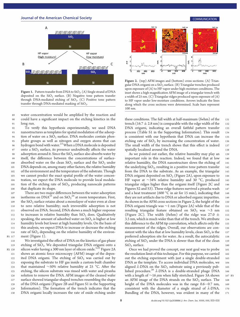
24 at room temperature. First,109 the SiO2 surface retains about a monolayer of water even at close110 to zero relative humidity; such irreversible adsorption is not111 observed on DNA. Second, DNA shows a much higher response112 to increases in relative humidity than SiO2 does. Qualitatively113 speaking, the amount of adsorbed water on SiO2 is higher at low114 humidity levels but lower at high humidity levels. On the basis of115 this analysis, we expect DNA to increase or decrease the etching116 rate of SiO2 depending on the relative humidity of the environ-117 ment (Figure 1F1 ).118 We investigated the effect of DNA on the kinetics of gas-phase119 etching of SiO2. We deposited triangular DNA origami onto a120 silicon wafer having a 300 nm layer of silicon oxide.5,25 Figure 2F2 A121 shows an atomic force microscopy (AFM) image of the depos-122 ited DNA origami. The etching of SiO2 was carried out by123 exposing the substrate to HF gas inside a custom-built chamber124 that maintained ∼50% relative humidity at 25 �C. After the125 etching, the silicon substrate was rinsed with water and piranha126 solution to remove the DNA. AFM images of the cleaned wafer127 surface showed triangular-shaped trenches resembling the shape128 of the DNA origami (Figure 2B and Figure S1 in the Supporting129 Information). The formation of the trench indicates that the130 DNA origami locally increases the rate of oxide etching under
131these conditions. The full width at half-maximum (fwhm) of the132trench (16.7( 2.8 nm) is comparable with the edge width of the133DNA origami, indicating an overall faithful pattern transfer134process (Table S1 in the Supporting Information). This result135is consistent with our hypothesis that DNA can increase the136etching rate of SiO2 by increasing the concentration of water.137The small width of the trench shows that this effect is indeed138spatially localized around the DNA.139As we pointed out earlier, the relative humidity may play an140important role in this reaction. Indeed, we found that at low141relative humidity, the DNA nanostructure slows the etching of142the underlying SiO2, resulting in a positive tone pattern transfer143from the DNA to the substrate. As an example, the triangular144DNA origami deposited on SiO2 (Figure 2A), upon exposure to145HF vapor at ∼34% relative humidity and 30 �C, produced146triangular ridges higher than the origami itself (Figure 2C and147Figures S2 and S3). These ridge features survived a piranha wash148and a heat treatment (600 �C in air for 15 min), indicating that149they are not artifacts due to DNA or adsorbed organic impurities.150As shown in the AFM cross sections in Figure 2, the height of the151DNA origami triangle was ∼1 nm (Figure 2A) while that of the152resulting triangular feature obtained on SiO2 was ∼3 nm153(Figure 2C). The width (fwhm) of the ridge was 27.0 (1543.5 nm, which is much wider than that of the trench.We attribute155this difference to the AFM tip convolution, which affects only the156measurement of the ridges. Overall, our observations are con-157sistent with the idea that at low humidity levels, clean SiO2 is the158preferred adsorption site for water. As a result, the autocatalytic159etching of SiO2 under the DNA is slower than that of the clean160SiO2 surface.161Once we had proved the concept, our next goal was to probe162the resolution limit of this technique. For this purpose, we carried163out the etching experiment with just a single double-stranded164DNA as the template. To access individual DNA molecules, we165aligned λ-DNA on the SiO2 substrate using a previously pub-166lished procedure.26 λ-DNA is a double-stranded phage DNA167with a length of ∼16 μm when fully stretched. Figure 3 F3A shows168an AFM image of the DNA strands on the SiO2 surface. The169height of the DNA molecules was in the range 0.6�0.7 nm,170consistent with the diameter of a single strand of λ-DNA.171Bundling of the DNA, however, was evident in many of the
Figure 1. Pattern transfer fromDNA to SiO2. (A) Single strand of DNAdeposited on the SiO2 surface. (B) Negative tone pattern transferthrough DNA-mediated etching of SiO2. (C) Positive tone patterntransfer through DNA-mediated masking of SiO2.
Figure 2. (top) AFM images and (bottom) cross sections: (A) Trian-gular DNA origami on a SiO2 surface. (B) Triangular trenches producedupon exposure of (A) to HF vapor under high-moisture conditions. Theinset shows a high-magnification AFM image of a triangular trench witha width of 25 nm. (C) Triangular ridges produced upon exposure of (A)to HF vapor under low-moisture conditions. Arrows indicate the linesalong which the cross sections were determined. Scale bars represent100 nm.
Journal of the American Chemical Society COMMUNICATION
B dx.doi.org/10.1021/ja2038886 |J. Am. Chem. Soc. XXXX, XXX, 000–000

172 strands. After the etching under high-moisture conditions173 (∼50% relative humidity), long trenches were observed on the174 SiO2 surface (Figure 3B). The width of the trenches was mea-175 sured to be 23.5 ( 4.2 nm (Figure S4 and Table S1) though176 trenches with widths of less than 10 nmwere located (Figure S5).177 We believe that the bundled DNA strands produced the wide178 trenches while the narrower ones were formed by the single179 DNA strands.180 The etching experiment with the stretched λ-DNA was also181 carried out under low-moisture conditions (∼34% relative182 humidity). It was observed that even a single strand of λ-DNA183 can slow the etching of SiO2 underneath it. In one experiment,184 we imaged the exact same location before (Figure 3A) and after185 the etching (Figure 3C). The height of the ridge features after the186 etching was 2�4 nm, representing a 3�6� amplification of the187 height of the DNA template. More importantly, we observed a188 very faithful pattern transfer from the DNA template to the SiO2
189 substrate.190 Our proposed mechanism is supported by a kinetics study of191 the etching reaction under the low-moisture conditions (Figure 4F4 ).192 SiO2 substrates with aligned λ-DNA on the surface were etched193 for 5, 10, 15, and 20 min and imaged using tapping-mode AFM194 before and after the cleaning (piranha/heat-treatment) process.195 The difference in the twomeasurements (∼0.7 nm) indicates the
196presence of the DNA template throughout the reaction. An197induction period (∼5 min) was observed, and this was followed198by a rapid buildup of the ridge height, signifying the autocatalytic199nature of the reaction.21 At longer reaction times, however,200enough water was produced by the reaction to saturate the201surface, leading to an eventual decrease in the contrast. The202substrate temperature also plays a significant role in determining203the etching kinetics. We observed that the etching rate decreased204with increasing substrate temperature, likely as a result of the205decrease in water adsorption on the SiO2 surface. This observa-206tion further confirms our working hypothesis that the pattern207transfer from DNA to SiO2 substrate is due to the spatial208variation in the concentration of surface-adsorbed water.209In conclusion, we have demonstrated a new approach to210pattern transfer from DNA to SiO2. DNA was used to increase211or decrease the etching rate of SiO2, resulting in negative or212positive tone pattern transfers to the substrate, respectively. Our213still unoptimized conditions routinely produce 20 nm wide214trenches, which may be useful as nanofluidic channels.27,28 This215method, if applied to a much thinner SiO2 film, would produce a216patterned SiO2 layer that could be used as a mask for etching of217the underlying silicon substrate. We believe that this methodol-218ogy will open up new opportunities in using self-assembled soft219materials as templates for bottom-up nanofabrication, with the220possibility of achieving molecular-scale resolution.
221’ASSOCIATED CONTENT
222bS Supporting Information. Experimental details, additional223figures, and a table. This material is available free of charge via the224Internet at http://pubs.acs.org.
225’AUTHOR INFORMATION
226Corresponding [email protected]
228Author Contributions229
§These authors contributed equally.
230’ACKNOWLEDGMENT
231Financial support from the University of Pittsburgh is acknow-232ledged. We thank Keith Jones of Asylum Research for acquiring233some of the AFM images.
234’REFERENCES
235(1) http://www.itrs.net/Links/2007ITRS/Home2007.htm236(accessed April 2011).237(2) Seeman, N. C. Annu. Rev. Biochem. 2010, 79, 65–87.238(3) Hung, A. M.; Noh, H.; Cha, J. N.Nanoscale 2010, 2, 2530–2537.239(4) Voigt, N. V.; Tørring, T.; Rotaru, A.; Jacobsen, M. F.; Ravnsbæk,240J. B.; Subramani, R.; Mamdouh, W.; Kjems, J.; Mokhir, A.; Besenbacher,241F.; Gothelf, K. V. Nat. Nanotechnol. 2010, 5, 200–203.242(5) Hung, A. M.; Micheel, C. M.; Bozano, L. D.; Osterbur, L. W.;243Wallraff, G. M.; Cha, J. N. Nat. Nanotechnol. 2010, 5, 121–126.244(6) Sharma, J.; Chhabra, R.; Cheng, A.; Brownell, J.; Liu, Y.; Yan, H.245Science 2009, 323, 112–116.246(7) Maune, H. T.; Han, S.-p.; Barish, R. D.; Bockrath, M.; Goddard,247W. A., III; Rothemund, P. W. K.; Winfree, E. Nat. Nanotechnol. 2010,2485, 61–66.249(8) Zhang, J.; Liu, Y.; Ke, Y.; Yan, H. Nano Lett. 2006, 6, 248–251.250(9) Keren, K.; Berman, R. S.; Buchstab, E.; Sivan, U.; Braun, E.251Science 2003, 302, 1380–1382.
Figure 4. Temporal evolution of the height of the ridges obtained underlow-moisture conditions.Measurements were carried out before (SiO2 +DNA; black) and after (SiO2 only; red) cleaning of the surface.
Figure 3. (top) AFM images and (bottom) cross sections: (A) λ-DNAaligned on the SiO2 substrate. (B) Trenches produced after exposure of(A) to HF vapor under high-moisture conditions. The inset shows ahigh-magnification image of the trench. (C) Ridges produced afterexposure of (A) to HF vapor under low-moisture conditions. It shouldbe noted that this AFM image was obtained at exactly the same locationas the one in (A). Arrows indicate lines along which the cross sectionswere determined. Scale bars represent 1 μm.
Journal of the American Chemical Society COMMUNICATION
C dx.doi.org/10.1021/ja2038886 |J. Am. Chem. Soc. XXXX, XXX, 000–000

252 (10) Ding, B.; Deng, Z.; Yan, H.; Cabrini, S.; Zuckermann, R. N.;253 Bokor, J. J. Am. Chem. Soc. 2010, 132, 3248–3249.254 (11) Xin, H.;Woolley, A. T. J. Am. Chem. Soc. 2003, 125, 8710–8711.255 (12) Pal, S.; Deng, Z.; Ding, B.; Yan, H.; Liu, Y.Angew. Chem., Int. Ed.256 2010, 49, 2700–2704.257 (13) Yan, H.; Park, S. H.; Finkelstein, G.; Reif, J. H.; LaBean, T. H.258 Science 2003, 301, 1882–1884.259 (14) Ding, B.; Wu, H.; Xu, W.; Zhao, Z.; Liu, Y.; Yu, H.; Yan, H.260 Nano Lett. 2010, 10, 5065–5069.261 (15) He, Y.; Chen, Y.; Liu, H.; Ribbe, A. E.; Mao, C. J. Am. Chem. Soc.262 2005, 127, 12202–12203.263 (16) Kershner, R. J.; Bozano, L. D.; Micheel, C. M.; Hung, A. M.;264 Fornof, A. R.; Cha, J. N.; Rettner, C. T.; Bersani, M.; Frommer, J.;265 Rothemund, P. W. K.; Wallraff, G. M. Nat. Nanotechnol. 2009,266 4, 557–561.267 (17) Gerdon, A. E.; Oh, S. S.; Hsieh, K.; Ke, Y.; Yan, H.; Soh, H. T.268 Small 2009, 5, 1942–1946.269 (18) Becerril, H. A.; Woolley, A. T. Small 2007, 3, 1534–1538.270 (19) Deng, Z.; Mao, C. Angew. Chem., Int. Ed. 2004, 43, 4068–4070.271 (20) Lee, Y.-I.; Park, K.-H.; Lee, J.; Lee, C.-S.; Yoo, H. J.; Kim, C.-J.;272 Yoon, Y.-S. J. Microelectromech. Syst. 1997, 6, 226–233.273 (21) Handbook of Silicon Wafer Cleaning Technology, 2nd ed.;274 Reinhardt, K. A., Kern, W., Eds.; William Andrew: Norwich, NY,275 2008; pp 281�304.276 (22) Montano-Miranda, G.; Muscat, A. J. Diffus. Defect Data, Pt. B277 2003, 92, 207–210.278 (23) Balkose, D.; Alp, B.; Ulku, S. J. Therm. Anal. Calorim. 2008, 94,279 695–698.280 (24) Mizushima, S. Metrologia 2004, 41, 137–144.281 (25) Please see the Supporting Information for experimental details.282 (26) Deng, Z.; Mao, C. Nano Lett. 2003, 3, 1545–1548.283 (27) Xia, Q. F.; Morton, K. J.; Austin, R. H.; Chou, S. Y. Nano Lett.284 2008, 8, 3830–3833.285 (28) Nam, S.-K.; Lee, M.-H.; Lee, S.-H.; Lee, D.-J.; Rossnagel, S. M.;286 Kim, K.-B. Nano Lett. 2010, 10, 3324–3329.
Journal of the American Chemical Society COMMUNICATION
D dx.doi.org/10.1021/ja2038886 |J. Am. Chem. Soc. XXXX, XXX, 000–000


