Mold Design and Temperature Field Analysis on Electrical Current Sintering of Electrically...
6
Section 4 Others MOLD DESIGN AND TEMPERATURE FIELD ANALYSIS ON ELECTRIC CURRENT SINTERING OF ELECTRICALLY CONDUCTIVE POWDERS YANG Junyi, LI Yuanyuan, LI Xiaoqiang, Guo Liang *School of Mechani cal Engi neer ing, South China University o f Technology, Guangzhou 510640, China Fax: (86) 20-87112948, E-mail: [email protected] Keywords: Field activated sintering, temper ature field, fini te element modelling, powder metallurgy. Abstract In order to probe and improve temperature field during elect ric current sintering, high st ren gth ceramic and graphite were used respectively as female die during sintering. Experiments and finite element method (FEM) were conducted to characterize the electric current density, resistance heati g and temperature distribution in the s pe ci me n/ di e/ pu nc h. O bv io us ly higher heating r at e, higher final sintering temperature and higher gradient temperature w er e f oun d in sp ec im en s w he n h ig h st re ng th c er am ic s w as used as female die, compared with graphite female die under t he c on di ti on s of the same die dimension and sintering eliminate the differences as well as to improve heating rate of the specimen. The experimental res ults are in good agreement with calculated values by FEM, which indicates that FEM may be an effective analysis method to simulate temperature field o f electric current sintering. 1 Introduction Electric current sintering (ECS) techniques, especially spark plasma sintering (SPS), have shown some great mer its such as faster heating and cooling, shorter holding time, fewer p ro ce ssi ng steps, l owe r si nt er in g t em pe ra tu re , c on tr ol le d a tm os ph er e a nd e xt er na l p re ss , e li mi na ti on of the need for s in te ri ng a id s, a nd n ea r n et s ha pe c ap ab il it y [1]. T he y h av e been widely used in fabrication and investigation of magnetic m ate ria ls, C er am ic s, b ul k a mo rp ho us al loy , i nt er me ta ll ic c om po un ds , m eta l m at ri x c om pos it es , fu nc ti ona l g ra di en t materials (FGM), ultra-fine grained and nano st ruc tu re materials, and so on, which have shown excellent performance [2- 8]. Currently, the main die material for ECS is graphite because of its benefits such as high melting point, medium electric resistance, low cost and so on. However, graphite has d is ad va nt ag es f or s in te ri ng . It s l ow s tr en gt h m ak es g ra ph it e punch not bear a relatively high uniaxial-pressure, otherwise the horizontal pressure generated by uniaxial-press can destroy the female die or shorten its working- life. In addition, s in te ri ng v el oc it y is a ls o l ow er ed by l ow s in te ri ng p re ss ur e. A no th er a dv er se fa ct or o f graphite is its high thermal conductivity ( abo ut three times t ha n t ha t o f st ee l) w he n graphite is used in female die. Due to the high thermal c on du ct iv it y, its h ea t t ra ns fe r is fast, wh ic h a cc el er at es t he h ea t lo ss o f d ie s ur fa ce . So , w it ho ut a pp ro pr ia te i ns ul at ed measures, the temperature of g ra ph it e d ie is d if fi cu lt t o r is e, which the maximal pulsed electric current is relatively low. It can also be imagined that the heat transfer in powders, which c on ta ct i nt er io r di e su rf ac e, is a lso fa st b ec au se o f t he h igh thermal conductivity of graphite, this is one o f the causes that result in large te perature gradient in powders [9], in particular for SPS which has fast heating rate. It is known that the heat energy in powder specimen during ECS is transferred from graphite punches and comes from its Joule heat [10,11]. Hence, the heating rate may be greater when using high strength ceramic die, becaus of its lower thermal conductivity and higher electrical resistance compared with graphite material . This makes lower electric current sintering possible. In this paper, to further clarify the advantages of cer amics die , both experime ts and FEM were adopted to ana yse the temperature field during electric current sintering of electrically conductive powders. 2 E xp er im en ta l s tu dy Experiments were carried out using an e le ct ri c c ur re nt sintering equipment, which had a maximal uniaxial-pressure o f 1 OOOKN. T he p ow er sup pl y c ou ld p ro vi de a p ul se d d ire ct e le ct ri c c ur re nt u p t o 3 00 0 A t hr ou gh t he r am s i nt o t he d ie se t that contained specimen. Fig.l shows the Schematic diagram o f heating system. A 5 mm thick celluloid plane was used to separate graphite punch electrode from the system. Graphite and alumina ceramic were adopted as female die materials respectively. Since the thermal stress generated by the temperature difference between int erior and outer die surface can destroy the die when it is beyond the ceramics thermal shock resistance [11]. In this paper alumina ceramic die surface was enveloped by iron sheath by thermal interference fit. A thermocouple was placed 3mm away from the top of the lower punch. E xpe ri me nt al p ar am et er s: t he ba se , d ut y r at io, f re que ncy , holding time and peak of pulsed direct current were 360 A, 50 %, 50Hz, 6minutes and 2400 A, respectively. Uniaxial
Transcript of Mold Design and Temperature Field Analysis on Electrical Current Sintering of Electrically...
8/2/2019 Mold Design and Temperature Field Analysis on Electrical Current Sintering of Electrically Conductive Powders
http://slidepdf.com/reader/full/mold-design-and-temperature-field-analysis-on-electrical-current-sintering 1/6
Section 4 Others
MOLD DESIGNAND TEMPERATURE FIELD ANALYSIS ON
ELECTRIC CURRENT SINTERING OF ELECTRICALLY
CONDUCTIVE POWDERS
YANG Junyi, LI Yuanyuan, LI Xiaoqiang, Guo Liang
*School ofMechanical Engineering, South China University ofTechnology, Guangzhou 510640, China
Fax: (86) 20-87112948, E-mail: [email protected]
Keywords: Field activated sintering, temperature field, finite
element modelling, powder metallurgy.
Abstract
In order to probe and improve temperature field during
electric current sintering, high strength ceramic and graphite
were used respectively as female die during sintering.
Experiments and finite element method (FEM) were
conducted to characterize the electric current density,
resistance heating and temperature distribution in the
specimen/die/punch. Obviously higher heating rate, higher
final sintering temperature and higher gradient temperature
were found in specimens when high strength ceramics was
used as female die, compared with graphite female die under
the conditions of the same die dimension and sintering
parameters. A composite die was proposed to reduce and even
eliminate the differences as well as to improve heating rate ofthe specimen. The experimental results are in good agreement
with calculated values by FEM, which indicates that FEM
may be an effective analysis method to simulate temperature
field of electric current sintering.
1 Introduction
Electric current sintering (ECS) techniques, especially spark
plasma sintering (SPS), have shown some great merits such as
faster heating and cooling, shorter holding time, fewer
processing steps, lower sintering temperature, controlled
atmosphere and external press, elimination of the need for
sintering aids, and near net shape capability [1]. They have
been widely used in fabrication and investigation of magneticmaterials, Ceramics, bulk amorphous alloy, intermetallic
compounds, metal matrix composites , functional gradient
materials (FGM), ul tra-fine grained and nanostructured
materials, and so on, which have shown excellent
performance [2-8].
Currently, the main die material for ECS is graphite because
of its benefits such as high melting point, medium electric
resistance, low cost and so on. However, graphite has
disadvantages for sintering. Its low strength makes graphite
punch not bear a relatively high uniaxial-pressure, otherwise
the horizontal pressure generated by uniaxial-press can
destroy the female die or shorten its working-life. In addition,
sintering velocity is also lowered by low sintering pressure.
Another adverse factor of graphite is its high thermal
conductivity (about three t imes than that of steel) when
graphite is used in female die. Due to the high thermal
conductivity, its heat transfer is fast, which accelerates theheat loss of die surface. So, without appropriate insulated
measures, the temperature of graphite die is difficult to rise,
particularly for those electrical current sintering techniques in
which the maximal pulsed electric current is relatively low. It
can also be imagined that the heat transfer in powders, which
contact interior die surface, is also fast because of the high
thermal conductivity of graphite, this is one of the causes that
result in large temperature gradient in powders [9], in
particular for SPS which has fast heating rate. It is known that
the heat energy in powder specimen during ECS is transferred
from graphite punches and comes from its Joule heat [10,11].
Hence, the heating rate may be greater when using high
strength ceramic die, because of its lower thermal
conductivity and higher electrical resistance compared withgraphite material. This makes lower electric current sintering
possible.
In this paper, to further clarify the advantages of ceramics die,
both experiments and FEM were adopted to analyse the
temperature field during electric current sintering of
electrically conductive powders.
2 Experimental study
Experiments were carried out using an electric current
sintering equipment, which had a maximal uniaxial-pressure
of 1OOOKN. The power supply could provide a pulsed direct
electric current up to 3000 A through the rams into the die set
that contained specimen. Fig.l shows the Schematic diagramof heating system. A 5 mm thick celluloid plane was used to
separate graphite punch electrode from the system. Graphite
and alumina ceramic were adopted as female die materia ls
respectively. Since the thermal stress generated by the
temperature difference between interior and outer die surface
can destroy the die when it is beyond the ceramics thermal
shock resistance [11]. In this paper alumina ceramic die
surface was enveloped by iron sheath by thermal interference
fit. A thermocouple was placed 3mm away from the top of the
lower punch.
Experimental parameters: the base, duty ratio, frequency,
holding time and peak of pulsed direct current were 360 A, 50
%, 50Hz, 6minutes and 2400 A, respectively. Uniaxial
8/2/2019 Mold Design and Temperature Field Analysis on Electrical Current Sintering of Electrically Conductive Powders
http://slidepdf.com/reader/full/mold-design-and-temperature-field-analysis-on-electrical-current-sintering 2/6
International Technology and Innovation Conference 2006
pressure was 30MPa and was supplied throughout sintering.
The sintering temperature was measured every 30 seconds via
the thermocouple. And the whole sintering was carried out in
the air.CelluloidPlane
/ Upper PunchElectrode
Lower PunchEletrode
Fig.l: schematic diagram of heating system
of electric current sintering equipment.
3 Finite element simulation
The heat transfer during electric current sintering can be
considered as three dimensional transient heat transfer in a
long cylinder which had heat source. Due to its symmetry, it
can be simplified to two dimensional axisymmetric transient
heat transfer, and the heat energy was offered by Joule heat
generated by electric current through it.
The transient heat transfer equation was described by the
energy balance equation [12]:
!.-(re r) .!.!..(n 8r)+!..(A 8 r ) + ~ (I )at rOr Or Oz Oz
Where p, p ' t , T and A represents the density, specific
heat, time, temperature, thermal conductivity, respectively.
#fis the heat produced by an internal heat source in unit time
and volume.
The current distribution is expressed by Kirchhoffs law
8(rir ) z =r az
Where irand iz represent the current density in the radial and
axial directions, respectively. The specific power #fis related
to the current density by Ohm's law
#f= irPr izpz
Where Pr and Pzare the electrical resistivity in radial and
axial directions, respectively.
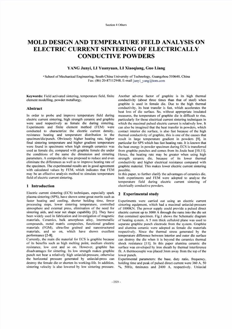
In order to simplify problem and save solved time, we
assumed that temperature and the electric potential were
continuous at the interface, that was to say, the thermal and
electric contact resistance can be ignored. Thermal
conductivity and electrical resistivity were functions of
temperature only. Due to powder volume change derived
from densification process, which was an extremely
complicated process, we assumed there was no volume
change but only density change. So, density change of
powders can be considered as volume change. Fig.2 shows
FE model, the thermoelectrical properties of materials were
given in table.1 [8,9,13]. The boundary conditions for
temperature and electric field were given as follows.
Initial and boundary conditions for temperature field: (a)
T(to) =293 K; (b) At the interface between upper (lower)
punch and celluloid plane, - 0; (c) At the
outer surfaces of all parts,
- n· £a s4amb -
4) •
Where n is the normal vector; h denotes nature convection
heat transfer coefficient, being 50 W/m K; ~ n and Tamb
represent the external and ambient temperature,
~ n =Tamb =293K; is emissivity, being 0.85; as is the
Stefan-Boltzmann constant, being 5.669 xIO-8W/m2K4•
Initial and boundary conditions for electric field: (a)
(t0) (b) At the interface between upper punch and
celluloid plane, - = where is current density,
J is inward current density; (c) At the interface between
lower punch and celluloid plane, V=O; (d) At the outer
surfaces of all components, n · =The model of temperature field during electric current
sintering was built by Electro-Thermal Interaction module in
FEM analysis software COMSOL Multiphysics. The virtual
modeling was set up by Drawing functional module in two
dimensional axisymmetric coordinates. Sintering variables,
material properties and boundary conditions were set in
Expressions, Subdomain Settings and Boundary Settings
functional modules, respectively. And the meshing (Fig.2)
was executed by mesh menu.
Fig.2: mesh partition.
4 Results and discussion
4.1 Electric current distribution
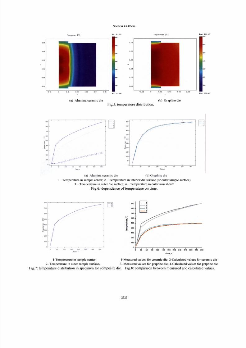
A series of simulations were performed. Fist the results
without thermal contact resistance at the interface were
presented. Current density distribution played a very
important role during electric current sintering since it
directly effected the distributions of heating rate and
temperature. Fig. 3 shows the magnitude of electric current in
the electrode/graphite plate/specimen/die/punch. The results
showed that the direction of the current in punches was
vertical for both alumina ceramic die and graphite die.
However, for alumina ceramic die, the electric current density
8/2/2019 Mold Design and Temperature Field Analysis on Electrical Current Sintering of Electrically Conductive Powders
http://slidepdf.com/reader/full/mold-design-and-temperature-field-analysis-on-electrical-current-sintering 3/6
Section 4 Others
was higher in the punches and exhibited a maximum at the
outside r i m ~ fewer electric current went through the alumina
ceramic die and iron sheath. For graphite d i e ~ the area with a
current flow in the horizontal direction was at the top of the
punch and at the contact of the punch with the top surface of
the d i e ~ electric current density was approximate except
outside rim of graphite punches which exhibited a m a x i m u m ~the specimen and the die were essentially in a parallel electric
network. The current path depended primarily on the ratio of
resistance of punch and d i e ~ i . e . ~ the electric conductivity of
the die and punch and the conductive cross section areas of
each component. Because the graphite punch was equally
conductive as the d i e ~ the majority of the current was diverted
to that which had a larger cross section area. As a w h o l e ~electric current density in punch for graphite die was less than
that of alumina ceramic die under the same conditions of die
dimension and sintering parameters. As shown in F i g . 3 ~ it was
also seen that the total valueof
current density in punch foralumina ceramic die was larger than that of graphite die.
4.2 Joule heat distribution
Fig. 4 depicts the Joule heat generation in punch/sample/die.
For alumina ceramic die, the amount of Joule heat caused by
the punches was obviously higher than those by specimen and
die. Since the most of the Joule heat energy formed in the
p u n c h e s ~ the specimen was indirectly heated by thermal
conduction from the punches. However, for graphite d i e ~ the
values of the Joule heat in p u n c h e s ~ specimen and die were
approximate except for in the part of punches unenveloped by
the die, and the specimen was heated mainly by thermal
conduction from the punches and die. As shown in F i g . 3 ~ the
amount of the Joule heat in punches was larger when alumina
ceramic was used as die material replacing graphite.
From Fig.3 and F i g . 4 ~ the components were found having a
higher current density and correspondingly higher Joule
heating.
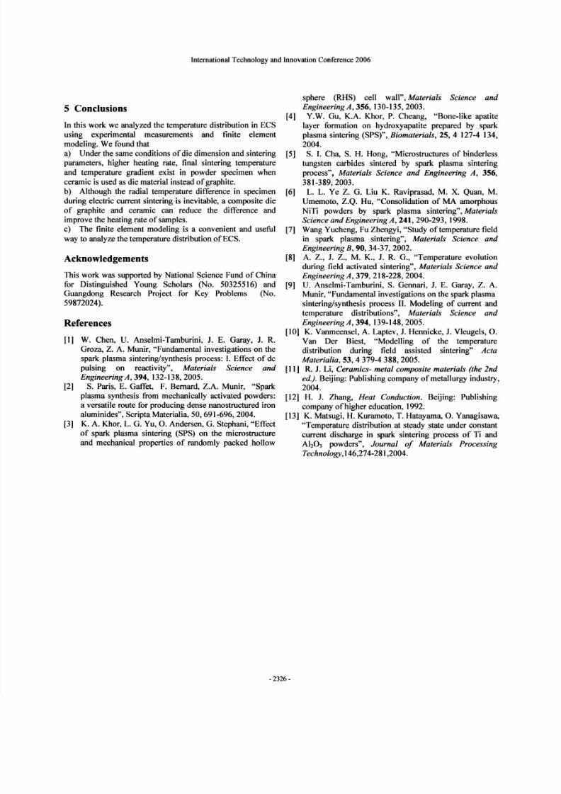
4.3 Temperature distribution
The temperature distribution in punch/specimen/die assembly
was characterized by the interplay of Joule heat generation
and heat transfer. Heat was mostly removed from the
punch/die/sample assembly via radiation and convection to
the ambient. As shown in Fig.5, for respectively alumina
ceramic die and graphite die, the part of punches close to the
specimen experienced the highest t e m p e r a t u r e ~ the specimen
experienced the medium temperature and the minimum
temperature was the one placed on the out die surface. is
implicit that Ti powder specimen is indirectly heated by
thermal conduction from the punches. For alumina ceramic
die, the highest temperature was about 900 °C the mean
temperature of specimen was above 850°C ;But for graphite
d i e ~ the maximum of temperature was about 500°C ~ t h e mean
temperature of specimen was less than 500°C .From Fig.5, we
also can see, temperature gradients were evidently in
punch/specimen/die for alumina ceramic d i e ~ compared with
graphite die.
Fig.6 shows temperature distribution in sample c e n t e r ~interior and outer die surface, outer iron sheath surface in
radial direction with time. For respectively alumina ceramic
die and graphite d i e ~ heating rate in the sample center and
interior die surface was very fast in the initial stage of
sintering. With prolonging of sintering t i m e ~ heating rate
reduced s l o w l y ~ but still remained a high value. As shown in
F i g . 6 ~ for alumina ceramics d i e ~ heating rate was obviously
higher than that of graphite d i e ~ but larger temperature
difference (about II 2°C) between center and outer sample
surface was found. This larger temperature difference may be
influence the consistency of the structure and performance of
the s a m p l e ~ in particular in the intermediate and final stage of
sintering.
From above results of temperature distribution, we knew that
alumina ceramic with lower electrical conductivity and lower
thermal conductivity may obviously improve heating rate andfinal sintering temperature in s p e c i m e n ~ but bring larger radial
temperature gradient in the sample. The reason may b e based
on above analysis of electrical current and Joule heat, the
punches experienced larger current density and Joule heat
generation for alumina c e r a m i c ~ resulting in faster heating
rate in specimen compared with graphite die; On the other
h a n d ~ heat loss of outer specimen was not supplied enough by
alumina ceramics die because of its fewer Joule heat
generation, this may result in relatively larger temperature
difference between center and surface of sample. When using
graphite d i e ~ due to existing Joule heat in graphite die
enveloping s p e c i m e n ~ the heat loss outer specimen was less
and resulting in lower temperature gradient in sample.
In this way, if combining the merits of graphite and c e r a m i c s ~we can design composite die which can not only improve
heating rate but also decrease temperature gradient under the
conditions of the same die dimension and sintering
p a r a m e t e r s ~ compared with graphite die and ceramics die.
Fig.7 shows temperature distribution of the specimen with
time using a composite die of graphite and ShN4 ceramic,
temperature difference between center and outer surface of
the sample was obviously lower (about 3 0 ° c ) ~ and the heating
rate was higher, compared with single ceramic die and
graphite die.
Fig.8 depicts the contrast between measured value and
calculated value by FEM. The finite element simulation with
no thermal contact resistance was found to be in reasonably
good agreement with experimental value in the range ofallowable error. Experimental observation and model results
showed that an almost linear increase of inside temperatures
on surface in the intermediate and final stage of sintering. In
the initial stage of s i n t e r i n g ~ the heating rates by experiment
and simulation were very fast due to large Joule heating
generated by large resistance. The measure value was higher
than calculation, the reason may be that: (I ) Overestimation
of air convection heat transfer coefficient between heating
system surface and ambient;(2) the effect of thermal contact
resistance on heat transfer had no not been considered.
8/2/2019 Mold Design and Temperature Field Analysis on Electrical Current Sintering of Electrically Conductive Powders
http://slidepdf.com/reader/full/mold-design-and-temperature-field-analysis-on-electrical-current-sintering 4/6
International Technology and Innovation Conference 2006
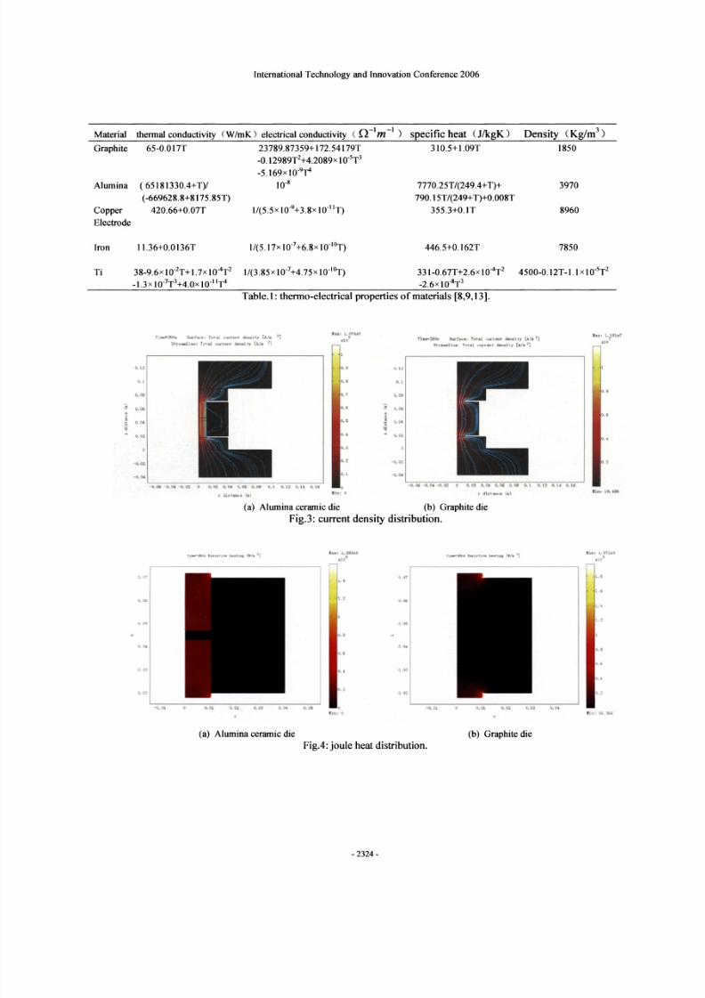
Material thermal conductivity (W/mK) electrical conductivity specific heat (J/kgK) Density3
)
3970
8960
1850
7770.25T/(249.4+T)+
790.15T/(249+T)+0.008T
355.3+0.IT/(5.5X 10-9+3.8x 10·IIT)
( 65181330.4+T)/
(-669628.8+8175.85T)
420.66+0.07T
Alumina
Graphite 65-0.0l7T 23789.87359+172.54179T 310.5+1.09T
-0.12989T
2
+4.2089x 10⁻⁵T3
-5.169x10⁻⁹y4
10-8
Copper
Electrode
[ron 11.36+0.0136T 446.5+0.162T 7850
Ti 38-9.6x 10⁻²T+1.7x 10⁻⁴T2
-1.3x I0-7T3+4.Ox 10·IIT4
1I(3.85x 10⁻⁷+4.75x 10-IOT) 331-0.67T+2.6x 10⁻⁴T2
-2.6x 10⁻⁸T3
4500-0.12T-1.1 x10⁻⁵T2
Table. 1: thermo-electrical properties ofmaterials [8,9,13].
In :lu :
CUi
0.6
(a) Alumina ceramic die (b) Graphite die
Fig.3: current density distribution.
In :
\t.i)$
lin:
lu :
1. 2
O.!
0.2
O.·fX
I.i!j;
(a) Alumina ceramic die
Fig.4: joule heat distribution.
(b) Graphite die
8/2/2019 Mold Design and Temperature Field Analysis on Electrical Current Sintering of Electrically Conductive Powders
http://slidepdf.com/reader/full/mold-design-and-temperature-field-analysis-on-electrical-current-sintering 5/6
8/2/2019 Mold Design and Temperature Field Analysis on Electrical Current Sintering of Electrically Conductive Powders
http://slidepdf.com/reader/full/mold-design-and-temperature-field-analysis-on-electrical-current-sintering 6/6
International Technology and Innovation Conference 2006
5 Conclusions
In this work we analyzed the temperature distribution in ECS
using experimental measurements and finite element
modeling. We found that
a) Under the same conditions of die dimension and sintering
parameters, higher heating rate, final sintering temperature
and temperature gradient exist in powder specimen when
ceramic is used as die material instead ofgraphite.
b) Although the radial temperature difference in specimen
during electric current sintering is inevitable, a composite die
of graphite and ceramic can reduce the difference and
improve the heating rate of samples.
c) The finite element modeling is a convenient and useful
way to analyze the temperature distributionof ECS.
AcknowledgementsThis work was supported by National Science Fund of China
for Distinguished Young Scholars (No. 50325516) and
Guangdong Research Project for Key Problems (No.
59872024).
References
[1] W. Chen, U. Anselmi-Tamburini, 1. E. Garay, 1. R.
Groza, Z. A. Munir, "Fundamental investigations on the
spark plasma sintering/synthesis process: Effect of dc
pulsing on reactivity", Materials Science and
Engineering A, 394, 132-138,2005.
[2] S. Paris, E. Gaffet, F. Bernard, Z.A. Munir, "Spark
plasma synthesis from mechanically activated powders:
a versatile route for producing dense nanostructured iron
aluminides", ScriptaMaterialia, 50,691-696, 2004.
[3] K. A. Khor, L. G. Yu, Andersen, G. Stephani, "Effect
of spark plasma sintering (SPS) on the microstructure
and mechanical properties of randomly packed hollow
sphere (RHS) cell wall", Materials Science and
Engineering A, 356, 130-135, 2003.
[4] Y.W. Gu, K.A. Khor, P. Cheang, "Bone-like apatite
layer formation on hydroxyapatite prepared by spark
plasma sintering (SPS)", Biomaterials, 25, 4 127-4 134,
2004.
[5] S. Cha, S. H. Hong, "Microstructures of binderless
tungsten carbides sintered by spark plasma sintering
process", Materials Science and Engineering A, 356,
381-389, 2003.
[6] L. L. Ye Z. G. Liu K. Raviprasad, M. X. Quan, M.
Umemoto, Z.Q. Hu, "Consolidation of amorphous
NiTi powders by spark p lasma sintering", Materials
Science andEngineeringA, 241, 290-293, 1998.
[7] Wang Yucheng, Fu Zhengyi, "Study of temperature field
in spark plasma sintering", Materials Science and
Engineering 90, 34-37, 2002.
[8] A. Z., 1. Z., M. K., J. R. G., "Temperature evolutionduring field activated sintering", Materials Science and
Engineering A, 379, 218-228, 2004.
[9] U. Anselmi-Tamburini, S. Gennari, 1. E. Garay, Z. A.
Munir, "Fundamental investigations on the spark plasma
sintering/synthesis process Modeling of current and
temperature distributions", Materials Science and
Engineering A, 394, 139-148, 2005.
[10] K. Vanmeensel, A. Laptev, 1. Hennicke, 1. Vleugels, O.
Van Der Biest, "Modelling of the temperature
distribution during field assisted sintering" Acta
Materialia, 53, 4 379-4 388, 2005.
[11] R. J. Li, Ceramics- metal composite materials (the 2nd
ed.). Beijing: Publishing company ofmetallurgy industry,
2004.[12] H. 1. Zhang, Heat Conduction. Beijing: Publishing
company ofhigher education, 1992.
[13] K. Matsugi, H. Kuramoto, T. Hatayama, O. Yanagisawa,
"Temperature distribution at steady state under constant
current discharge in spark sintering process of Ti and
Ah03 powders", Journal of Materials Processing
Technology,146,274-281,2004.


![Effect of sintering temperature on microstructure and electrical ... · sintered SrBi 2Ta 2O 9 ceramic was reported [30]. Hydrothermal synthesis of ceramic powders has gained considerable](https://static.fdocuments.net/doc/165x107/5e4c4aff753cfb3ad22691fb/effect-of-sintering-temperature-on-microstructure-and-electrical-sintered-srbi.jpg)
![Morphology of polymeric powders in Laser Sintering (LS ... · mechanical properties, elevated thermal stability and outstanding chemical resistance[28]. PA2200 is a polyamide 12 polymer.](https://static.fdocuments.net/doc/165x107/5f7604a001991c39e7656416/morphology-of-polymeric-powders-in-laser-sintering-ls-mechanical-properties.jpg)