MOHAMAD RIJAL HAMID Doctor of Philosophy...
276
WIDEBAND RECONFIGURABLE ANTENNAS by MOHAMAD RIJAL HAMID A Thesis submitted to The University of Birmingham For the degree of Doctor of Philosophy (PhD) School of Electronic, Electrical and Computer Engineering College of Engineering and Physical Sciences The University of Birmingham May 2011
Transcript of MOHAMAD RIJAL HAMID Doctor of Philosophy...

WIDEBAND RECONFIGURABLE
ANTENNAS
by
MOHAMAD RIJAL HAMID
A Thesis submitted to
The University of Birmingham
For the degree of
Doctor of Philosophy (PhD)
School of Electronic, Electrical and
Computer Engineering
College of Engineering and Physical
Sciences
The University of Birmingham
May 2011

University of Birmingham Research Archive
e-theses repository This unpublished thesis/dissertation is copyright of the author and/or third parties. The intellectual property rights of the author or third parties in respect of this work are as defined by The Copyright Designs and Patents Act 1988 or as modified by any successor legislation. Any use made of information contained in this thesis/dissertation must be in accordance with that legislation and must be properly acknowledged. Further distribution or reproduction in any format is prohibited without the permission of the copyright holder.
ii
ABSTRACT
The work described in this thesis concerns the combining of wideband and reconfigurable
narrow band functionality into a single antenna. This concept may be useful in reducing
size and to give flexibility to a wireless terminal to operate in several different modes. The
approach also offers additional pre-filtering to the front-end, which reduces the
interference levels at the receiver, giving them a significant advantage over fixed non
reconfigurable transceivers. Wideband-narrowband reconfiguration is potentially useful for
future wireless communications such as software defined radio and cognitive radio, since
they may employ wideband sensing and reconfigurable narrowband communications.
Five novel reconfigurable antennas are presented. One is a switchable log periodic patch
array and four are Vivaldi antennas with various forms of reconfiguration. The log periodic
is reconfigured by placing switches between the patches and the feed line whilst the
Vivaldi antenna has switched resonators controlling the current in the edges of the tapered
slots. Wideband to various narrowband functions, wideband with a tunable band rejection
having a very wide tuning ratio, and combined three function wide, narrow and tunable
band rejection in a single antenna are demonstrated. Prototypes are presented with PIN
diode switches, varactors, fixed capacitor or hard wire switches. Measured and simulated
results with a very good agreement are presented, thus verifying the proposed concepts.

iii
ACKNOWLEDGMENTS
I would like to express my deepest gratitude to my supervisors Dr Peter Gardner, Reader in
Microwave Engineering and Prof Peter S. Hall, Electronic Electrical Computer
Engineering, University of Birmingham for their valuable guidance, advice, understanding
and excellent support. It has been an honour for me to be supervised by people with such
wide knowledge and top notch ideas.
I also wish to thank my colleagues Dr James Kelly, Dr Yuriy Nechayev, Dr Farid Ghanem
and everyone in the Cognitive Radio group, University of Birmingham, for sharing ideas
and discussions during the period of completing the studies.
It is a pleasure to thank Mr Alan Yates for his technical support and for teaching me how
to fabricate my own antennas.
I owe my loving and sincere thanks to my mother Sadariah Husin, my wife Zuhaidah
Shahrin, my children Fatih, Fawwaz, Anis and Khalis. My special gratitude and loving
thanks are also due to my sisters. Their prays and duas, support, encouragement,
understanding and sacrifices have helped and motivated me a lot throughout the entire time
I worked on my thesis.
Last but not least, I am also grateful to the Universiti Teknologi Malaysia (UTM) for the
financial support and PhD sponsorship.

iv
PUBLICATIONS
Journals
1. Hamid M. R., Gardner P., Hall P. S., and Ghanem F., "Vivaldi Antenna with
Integrated Switchable Pass Band Resonator," in press, IEEE Transactions on
Antennas and Propagation, 2011.
2. Hamid, M R, Gardner, P, Hall, P S and Ghanem, F, “Switched Band Vivaldi
Antenna”, IEEE Transactions on Antennas and Propagation, Volume 53, No. 5,
2011
3. Hamid, M R, Gardner, P, Hall, P S and Ghanem, F, “Vivaldi with Tunable Narrow
band Rejection”, Microwave and Optical Technology Letters, Volume 53, No 5,
2011
4. Hamid, M R, Hall, P S and Gardner, P, “Frequency Reconfigurable Log Periodic
Patch Array”, Electronics Letters Volume 46, Issue 25, Dec 2010
5. Hamid, M R, Gardner, P, Hall, P S and Ghanem, F, “Multi-Mode Vivaldi
Antenna”, Electronics Letters Volume 46, Issue 21, Oct 2010
6. Hamid, M R, Hall, P S, Gardner, P and Ghanem, F, “Switchable Filtering in
Vivaldi Antenna”, Electronics Letters Volume 46, Issue 7, April 2010
7. Hamid, M R, Gardner, P, Hall, P S and Ghanem, F, “Reconfigurable Vivaldi
Antenna”, Microwave and Optical Technology Letters, Volume 52, Issue 4, April
2010
8. Hamid, M R, Hall, P S, Gardner, P and Ghanem, F, “Switched WLAN-Wideband
Tapered Slot Antenna”, Electronics Letters Volume 46, Issue 1, Jan 2010
Conferences
1. Hamid, M R, Gardner, P, Hall, P S and Ghanem, F, “Reconfigurable Vivaldi
Antenna with Tunable Band Stop”, IEEE International Workshop on Antenna
Technology 7-9 March, 2011, Hong Kong
2. Hamid, M R, Gardner, P, Hall, P S and Ghanem, F, “Review of Reconfigurable
Vivaldi Antenna”, IEEE International Symposium on Antennas and Propagation,
APS 2010, Toronto, Canada, July 2010
3. Hamid, M R, Gardner, P, Hall, P S and Ghanem, F, “Reconfigurable Slot Line
Filter”, The IET seminar on Passive RF and Microwave Components, Birmingham,
UK, April 2010
4. Hamid, M R, Hall, P S, Gardner, P and Ghanem, F, “Frequency Reconfigurable
Vivaldi Antenna”, European Conference on Antennas and Propagation, Eucap 2010
Barcelona, Spain, April 2010
5. Hamid, M R, Gardner, P and Hall, P S, Ghanem, F, “Switchable Wideband-
Narrowband Tapered Slot Antenna”, Loughborough Antenna and Propagation
Conference, Loughborough, UK, 16-17 Nov 2009

v
6. Hamid, M R, Gardner, P and Hall, P S, “Reconfigurable Log Periodic Aperture
Fed Microstrip Antenna”, Loughborough Antenna and Propagation Conference,
Loughborough, UK, 16-17 Nov 2009
7. Tariq A., Hamid M.R. and Shiraz H.G., “Reconfigurable Monopole Antenna”,
accepted in European Conference on Antennas and Propagation, Eucap 2011
Rome, Italy, 11-15 April 2011
8. Hall P S, Hamid M R, Ghanem F, Mirkamali A and Gardner P
“RECONFIGURATION OF VIVALDI AND LOG PERIODIC ANTENNAS” in
Proc. Allerton Antenna Symposium 09, USA, 22-23 Sept 2009,
9. Gardner P., Hamid M. R., Hall P. S., Kelly J., Ghanem F., and Ebrahimi E.,
"Reconfigurable antennas for cognitive radio: requirements and potential design
approaches," in The IET seminar on Wideband, multiband antennas and arrays for
defence or civil applications, London, UK, Mar. 2008.
10. P. Hall, Z. H. Hu, P. Song, M. R. Hamid, and Z. Wang, “Creating reconfigurable
adaptive antennas for cognitive radio applications considering cost and portability”,
The IET Seminar on Cognitive Radio Communications, 4th Oct. 2010, London,
U.K.
11. Hall P S, Gardner P., Hu Z., Song P., Kelly J., Hamid M.R., ‘Reconfigurable
antennas for wideband wireless systems’ Adaptable and Tunable Antenna
Technology for Handsets and Mobile Computing Products Savoy Place, London,
22 Oct 2009,
12. Hall P. S., Gardner P., Kelly J., Ebrahimi E., Hamid M. R., Ghanem F., Herraiz-
Martinez F. J. and Segovia-Vargas D., “Reconfigurable Antenna Challenges for
Future Radio Systems," in Proc. EuCAP 09, Berlin, Germany, Mar. 2009.
13. Hall P. S., Gardner P., Kelly J., Ebrahimi E., Hamid M. R., and Ghanem F.,
"Antenna challenges in cognitive radio," (invited paper) in Proc. ISAP 08, Taiwan,
Oct. 2008.

vi
TABLE OF CONTENTS
CHAPTER 1 ......................................................................................................................... 1
INTRODUCTION ............................................................................................................... 1
1.1 Introduction ................................................................................................................ 1
1.2 Motivation ................................................................................................................... 2
1.3 Objective ..................................................................................................................... 2
1.4 Thesis outline .............................................................................................................. 3
CHAPTER 2 ......................................................................................................................... 6
BACKGROUND AND LITERATURE REVIEW ........................................................... 6
2.1 Introduction ................................................................................................................ 6
2.2 Wideband Antenna .................................................................................................... 8
2.2.1 Log Periodic Array ............................................................................................. 8
2.2.2 Vivaldi Antenna ............................................................................................... 13
2.3 Reconfigurable Antennas ........................................................................................ 17
2.3.1 Narrowband to narrowband reconfiguration .................................................... 18
2.3.2 Wideband to narrowband reconfiguration ........................................................ 24
2.3.3 Wideband to notch band reconfiguration ......................................................... 31
2.3.4 Wideband to wideband reconfiguration ........................................................... 36
2.4 Summary ................................................................................................................... 37
CHAPTER 3 ....................................................................................................................... 39
RECONFIGURABLE LOG PERIODIC APERTURE COUPLED PATCH ARRAY
............................................................................................................................................. 39
3.1 Introduction .............................................................................................................. 39
3.2 Motivation ................................................................................................................. 40
3.3 Structural Stop Band ............................................................................................... 42
3.4 Eliminating Structural Stop Band .......................................................................... 49
3.5 Scaling Factor and Element Bandwidth ................................................................ 53
3.6 Reconfigurable Log Periodic Aperture Coupled Patch Array Design ............... 55
3.7 Simulation Results ................................................................................................... 58
3.7.1 Improving Low Band Performances ................................................................ 63

vii
3.8 Measurement result ................................................................................................. 70
3.9 Summary ................................................................................................................... 79
CHAPTER 4 ....................................................................................................................... 81
WIDE-NARROW RECONFIGURABLE BAND MULTIPLE RING VIVALDI
ANTENNA .......................................................................................................................... 81
4.1 Introduction .............................................................................................................. 81
4.2 Wideband Antenna Design ..................................................................................... 82
4.3 Narrowband Agile Antenna Design ....................................................................... 84
4.4 Four Mode Reconfigurable Configuration ............................................................ 93
4.4.1 Narrow low band mode .................................................................................... 95
4.4.2 Narrow mid band mode .................................................................................... 96
4.4.3 Narrow high band mode ................................................................................... 97
4.5 Prototype Antenna ................................................................................................. 102
4.6 Results ..................................................................................................................... 104
4.7 Summary ................................................................................................................. 113
CHAPTER 5 ..................................................................................................................... 114
VIVALDI WITH SINGLE RING RESONATOR ........................................................ 114
5.1 Introduction ............................................................................................................ 114
5.2 Wideband Antenna Design ................................................................................... 115
5.3 Slot Line Resonator Design ................................................................................... 116
5.4 Seven Mode Reconfigurable Configuration ........................................................ 126
5.5 Antenna Construction and Measurements .......................................................... 141
5.6 Results ..................................................................................................................... 142
5.7 Summary ................................................................................................................. 155
CHAPTER 6 ..................................................................................................................... 156
VIVALDI WITH TUNABLE NARROW BAND REJECTION ................................. 156
6.1 Introduction ............................................................................................................ 156
6.2 Band Notch Resonator Design .............................................................................. 158
6.2.1 Length and width of the resonator .................................................................. 159
6.2.2 Resonator positions ........................................................................................ 160
6.2.3 Varactor positions ........................................................................................... 162

viii
6.3 Simulations and Experiments ............................................................................... 167
6.3.1 Fixed band notch ............................................................................................ 167
6.3.2 Tunable Notch ................................................................................................ 171
6.3.3 Multiple Varactor for Wider Tuning Range ................................................... 177
6.4 Electronic tuning .................................................................................................... 186
6.5 Summary ................................................................................................................. 189
CHAPTER 7 ..................................................................................................................... 191
COMBINED WIDE-NARROW-NOTCH BAND VIVALDI ANTENNA ................. 191
7.1 Introduction ............................................................................................................ 191
7.2 Antenna Design ...................................................................................................... 192
7.3 Antenna Operations and Results .......................................................................... 194
7.4 Summary ................................................................................................................. 207
CHAPTER 8 ..................................................................................................................... 208
CONCLUSIONS AND FUTURE WORK ..................................................................... 208
8.1 Conclusions ............................................................................................................. 208
8.1.1 Reconfigurable Log Periodic Patch Array [80, 81] ........................................ 208
8.1.2 Reconfigurable Vivaldi Antenna .................................................................... 209
8.1.2.1 Multiple position slot ring resonators [83-86] ........................................... 210
8.1.2.2 Single position switchable length slot ring resonators [87, 92] ................. 210
8.1.2.3 Microstrip line resonator [75, 88] .............................................................. 210
8.1.2.4 Combined ring and rectangular slot resonators [89, 93] ............................ 211
8.2 Future work ............................................................................................................ 212
REFERENCES ................................................................................................................. 217
APPENDICES ........................................................................ Error! Bookmark not defined.

ix
LIST OF FIGURES
Figure 2.1 Log periodic arrays (a) printed dipole [18] (solid conductors on top of substrate,
dotted on lower) (b) monopole array [19] (series feed on top of substrate, ground plane on
lower) ................................................................................................................................... 10
Figure 2.2 Log periodic patch array (a) electromagnetic coupled feed [21]- , (b) series
branch lines feed -[22] , and (c) aperture coupled feed - [23] types .................................... 11
Figure 2.3 Reconfigurable log periodic antenna (a) [18] (only conductors on top of
substrate shown), (b) [25] (only conductors on top of substrate shown), (c) [26] (grey-
conductors on top of substrate, light grey - on lower) ......................................................... 12
Figure 2.4 Band notch log periodic antennas, (a) [27], (b) [28] and (c) [29] (only
conductors on top of substrate shown) ................................................................................ 13
Figure 2.5 Vivaldi antenna showing microstrip feed (dash line) on the reverse side .......... 15
Figure 2.6 Antipodal Vivaldi [37] (black conductor on front of substrate, grey on back) .. 15
Figure 2.7 Typical simulated surface current distributions in Vivaldi excited at 3 GHz .... 16
Figure 2.8 Band notch Vivaldi antennas (a) slot stubs in edge [38], (b) u shaped slot in
conductors [39] .................................................................................................................... 17
Figure 2.9 Rotation controlled antenna (dark grey-conductor on top of substrate, light grey-
conductor on back) [7] ......................................................................................................... 24
Figure 2.10 Two ports wideband monopole (microstrip feed on top of substrate, CPW feed
and meandered slot on back [8] ........................................................................................... 25
Figure 2.11 Integrated PIFA and wideband monopole (grey – conductor on top of
substrate, dash- conductor on back) [53] ............................................................................. 26
Figure 2.12 Integrated slot antenna and wideband monopole (black-conductor on top of
substrate, grey-conductor on back [54] ................................................................................ 27
Figure 2.13 Integrated left hand loop and wideband monopole (dark grey-conductor on top
of substrate, light grey-conductor on back) [55] .................................................................. 27
Figure 2.14 Integrated narrow and wideband monopole (a) [56] and (b) [57] .................... 28
Figure 2.15 Switched ground plane patch antenna (grey- conductor on top of substrate,
black-conductor on back, S1, S2, S3 – switches) [58] .......................................................... 29

x
Figure 2.16 Switched annuli wideband slot antenna (black-conductor, grey-non conductor)
[59] ....................................................................................................................................... 29
Figure 2.17 Coupled resonator and feed line wideband monopole (light grey-conductor on
top of substrate, grey-conductor on back) [60] ................................................................... 30
Figure 2.18 RF impedance tuner [61] .................................................................................. 31
Figure 2.19 Integrated rectangular slot and wideband slot bow-tie [68] ............................. 33
Figure 2.20 (a) Circular monopole with switchable stubs [69] and (b) Rectangular
monopole with parasitic patch at the back (left-front view, right- rear view) [70] ............. 34
Figure 2.21 Planar wideband monopole perpendicular to ground plane (black-conductor,
white-non conductor, light grey-bias line at the back) [71] ................................................. 34
Figure 2.22 Planar monopole with short circuited microstrip stub [72] .............................. 35
Figure 2.23 (a) Pyramidal monopole with four slots [73], (b) Planar monopole with two
slot [74] ................................................................................................................................ 35
Figure 2.24 Wideband reconfigurable rolled planar monopole antenna (top – 3D view,
bottom – Side view with different spiral tightness) [76] ..................................................... 37
Figure 3.1 LPA arrangement on the taper shaped cylinder ................................................. 41
Figure 3.2 LPA arrangement on the straight shaped cylinder ............................................. 42
Figure 3.3 Simplified equivalent circuit of series patch in the transmission line ................ 43
Figure 3.4 Log periodic aperture coupled patch array, wf - feed line width, hf - feed line
substrate thickness, hp - patch substrate thickness, d – excess length, σ - free space spacing,
w - patch width, l - patch length, ws - aperture width, ls - aperture length ........................... 44
Figure 3.5 Single cell with a shunt load of periodic structure ............................................. 45
Figure 3.6 (a) Image impedance, Zi, (b) Attenuation, dα , (c) Phase, bd, ............................ 47
Figure 3.7 (a) Image impedance, |Zi| (b) Attenuation, dα (c) Phase, bd, ............................ 48
Figure 3.8 A cascaded single cells forming a log periodic structure ................................... 49
Figure 3.9 Transmission line with impedance modulation .................................................. 49
Figure 3.10 (a) Single cell of aperture coupled fed structure without impedance
modulation, (b) simulated S11 and S21, (c) Image impedance, |Zi|, (d) Attenuation, ad ....... 51

xi
Figure 3.11 (a) Single cell of aperture coupled fed structure with impedance modulation,
(b) Image impedance, |Zi|, (c) Attenuation, ad ..................................................................... 53
Figure 3.12 Efficiency of 10 elements array, 2.2=rε , wf = 2.38 mm, hf = 0.787 mm, hp =
1.575 mm, (d1 = 53.31 mm, 14.35=σ mm for 015.1=τ ), (d1 = 53.7 mm, 54.35=σ mm for
03.1=τ ), w1 = 20.25 mm, l1 = 27 mm, see Figure 2.4 for definition of the dimensional
parameters ............................................................................................................................ 54
Figure 3.13 Cross section of microstrip patch log periodic array with rohacell in the
middle to increase individual bandwidth ............................................................................. 55
Figure 3.14 Efficiency of 5 element array, 02.1=τ , 2.2=rε (for hf and hp), 09.1=rε (for
rohacell), wf = 2.38 mm, hf = 0.787 mm, hp = 0.254 mm, rohacell = 2 mm, d1 = 23.72 mm,
86.15=σ mm, w1 = 10.4 mm, l1 = 16 mm, ............................................................................ 55
Figure 3.15 Proposed antenna structure (a) Perspective view (b) Side view (c) Top
view, 02.1=τ , 2.2=rε (for hf and hp), 09.1=rε (for rohacell), wf = 2.38 mm, hf = 0.787
mm, hp = 0.254 mm, rohacell = 2 mm, d1 = 16.1 mm, 86.15=σ mm, w1 = 7 mm, l1 = 10.77
mm, ...................................................................................................................................... 57
Figure 3.16 Simulated wideband mode, (a) scattering parameters (b) efficiency ............... 59
Figure 3.17 Simulated effects of screening box on radiation pattern (H-plane) excited at 8.2
GHz, (a) without-, (b) with screening box ........................................................................... 60
Figure 3.18 Simulated wideband radiation pattern (H-plane) excited at (a) 7.1-, (b) 8.2-, (c)
9.4 GHz ................................................................................................................................ 61
Figure 3.19 Simulated efficiency for selected three frequency bands ................................. 62
Figure 3.20 Simulated radiation pattern (H-plane) for selected three frequency bands (a)
Low -, (b) Mid- and (c) High band ...................................................................................... 63
Figure 3.21 Modulated impedance feeder and the equivalent circuits ................................ 64
Figure 3.22 Pi equivalent circuits after slot is bridged, Sa – switch on slot ........................ 64
Figure 3.23 (a) A structural stop band and (b) an image impedance of a cell when slot is
closed ................................................................................................................................... 66
Figure 3.24 Modified line and its equivalent circuit, Sa – switch on slot ............................ 66

xii
Figure 3.25 (a) An image impedance and, (b) a structural stop band for the modified lines
of cell 19th
after slot is closed .............................................................................................. 67
Figure 3.26 Simulated low band mode efficiency before and after improvement .............. 68
Figure 3.27 Switch position, Sf – switch on feed, Sa – switch on slot ................................. 68
Figure 3.28 Simulated wideband efficiency before and after improvement of low band
mode ..................................................................................................................................... 69
Figure 3.29 Three selected narrow band of the proposed reconfigurable log periodic patch
array ..................................................................................................................................... 69
Figure 3.30 Measured wideband mode scattering parameters ............................................. 70
Figure 3.31 Wideband mode efficiency ............................................................................... 71
Figure 3.32 The selected three narrowband mode, (a) High band, (b) Mid band, and (c)
Low band ............................................................................................................................. 73
Figure 3.33 Out of band rejection in mid band mode .......................................................... 73
Figure 3.34 Proposed screening box where a copper tape is used to reasonably enclose the
lower substrate, hf into the shielding box ............................................................................. 74
Figure 3.35 Measured efficiency of the reconfigurable log periodic patch array ................ 74
Figure 3.36 Measured wideband efficiency on modified and unmodified line ................... 75
Figure 3.37 Wideband mode radiation pattern excited at (a) 7.1 GHz, (b) 8.2 GHz and (c)
9.4 GHz ................................................................................................................................ 77
Figure 3.38 Narrow band mode radiation pattern (a) Low band mode excited at 7.1 GHz,
(b) Mid band mode excited at 8.2 GHz and (c) High band mode excited at 9.4 GHz ......... 78
Figure 4.1 Non reconfigurable Vivaldi antenna, (a) front view, (b) rear view showing
microstrip feed ..................................................................................................................... 83
Figure 4.2 Simulated wideband non reconfigurable Vivaldi antenna ................................. 83
Figure 4.3 Simulated surface current distributions excited at 3GHz ................................... 84
Figure 4.4 Simulated surface current distributions after perturbation excited at 3GHz ...... 84
Figure 4.5 Slot shapes (a) ring-, (b) triangle-, (c) rectangle-, (d) thin rectangle shape ....... 85
Figure 4.6 Simulated admittance, |Y| of various slot shapes ............................................... 86
Figure 4.7 Simulated |S21| of various slot shapes ................................................................. 86
xiii
Figure 4.8 Simulated S21 of ring slot resonator (a) band stop (b) band pass (c) low pass;
(slot line width = 2 mm, ring outer radius = 10 mm, ring inner radius = 6 mm, small
connecting gap = 4 mm x 3.48 mm, small bridge[case (c) only] = 4 mm x 2 mm) ............ 88
Figure 4.9 Ring slot resonator (a) band stop (b) band pass (c) low pass ............................. 89
Figure 4.10 Simulated S11 of low band configurations (x = 9.55 mm) ................................ 89
Figure 4.11 Simulated S11 of high band configurations (x = 56.2 mm) ............................... 90
Figure 4.12 (a) Simulated antenna S11 when resonators at matched position, x = 23.69 (b)
resonators at x = 43.77 mm .................................................................................................. 91
Figure 4.13 Impedances associated in finding optimum ring slot position, ideal condition
when ZRS = ZSLOT .................................................................................................................. 92
Figure 4.14 (a) Vivaldi with different band pass ring slots; RS1 (ring outer radius = 12 mm,
ring inner radius = 8 mm, small connecting gap = 4 mm x 2.5 mm, x1 = 33.68 mm), RS2
(ring outer radius = 10 mm, ring inner radius = 6 mm, small connecting gap = 4 mm x 2.88
mm, x2 = 23.69 mm), RS3 (ring outer radius = 8.5 mm, ring inner radius = 5.5 mm, small
connecting gap = 3 mm x 2.5 mm, x3 = 18.59 mm), and RS4 (ring outer radius = 7 mm,
ring inner radius = 4 mm, small connecting gap = 3 mm x 2.32 mm, x4 = 10.37 mm), (b)
Simulated S11 of four band pass configurations at matched position .................................. 93
Figure 4.15 Four band reconfigurable antenna, (ring outer radius = 10 mm, ring inner
radius = 6 mm, small connecting gap = 4 mm x 3.5 mm, x1 = 9.55 mm, x2 = 33.73 mm, x3
= 56.2 mm, small bridge [the lowest slot only] = 4 mm x 2 mm) ....................................... 94
Figure 4.16 (a) Low band- (b) Mid band- (c) High band configuration .............................. 95
Figure 4.17 Tapered slot line voltages ................................................................................. 95
Figure 4.18 Low band dispersions curve, (attenuation and phase) ...................................... 96
Figure 4.19 Mid band dispersions curve, (attenuation and phase) ...................................... 97
Figure 4.20 High band dispersions curve, (attenuation and phase) ..................................... 97
Figure 4.21 Gain comparison between WR and ID antennas .............................................. 98
Figure 4.22 Gain comparison between PIN and ID antennas .............................................. 99
Figure 4.23 Simulated surface current distributions for (a) Wideband configuration excited
at 1.1GHz, (b) Low band configuration excited at 1.1GHz, (c) Wideband configuration

xiv
excited at 2.2GHz, (d) Mid band configuration excited at 2.2GHz, (e) Wideband
configuration excited at 3.1GHz, (d) High band configuration excited at 3.1GHz ........... 100
Figure 4.24 Simulated current distributions for the low band configuration excited at (a) 2
GHz and (b) 3 GHz ............................................................................................................ 101
Figure 4.25 Simulated current distributions for the mid band configuration excited at (a)
1.1 GHz and (b) 3 GHz ...................................................................................................... 101
Figure 4.26 Simulated current distributions for the high band configuration excited at (a)
1.1 GHz and (b) 2 GHz ...................................................................................................... 101
Figure 4.27 Prototype ........................................................................................................ 103
Figure 4.28 Spurious in S11 responses as a function of gap sizes. ..................................... 104
Figure 4.29 Simulated wideband mode S11 response of antenna with and without ring slots
........................................................................................................................................... 105
Figure 4.30 Simulated and measured wideband mode S11 ................................................ 105
Figure 4.31 Simulated and measured S11 of antenna in narrowband modes (a) Low band
state (b) Mid band state (c) High band state. ..................................................................... 107
Figure 4.32 Rejection in S11 as a function of substrate loss .............................................. 108
Figure 4.33 Rejection in S11 as a function of switch loss ................................................. 108
Figure 4.34 Measured low band gain of the proposed antenna ......................................... 109
Figure 4.35 Measured mid band gain of the proposed antenna ......................................... 110
Figure 4.36 Measured high band gain of the proposed antenna ........................................ 110
Figure 4.37 Radiation pattern. (a) Low band mode excited at 1.1 GHz, E-plane (left), H-
plane (right). (b) Mid band mode exited at 2.2 GHz, E-plane (left) , H-plane (right). (c)
High band mode excited at 3.1 GHz E-plane (left) , H-plane (right). (d) Wideband mode
excited at 2.0 GHz, E-plane (left) , H-plane (right). .......................................................... 112
Figure 5.1 Vivaldi antenna, (a) front view, (b) rear view showing microstrip feed. ........ 115
Figure 5.2 S11 of Vivaldi antenna in Figure 5.1 ................................................................. 116
Figure 5.3 Simulated surface current distribution at 2 GHz .............................................. 116
Figure 5.4 Slot ring resonator ............................................................................................ 117
Figure 5.5 RLC shunt circuits in series .............................................................................. 118

xv
Figure 5.6 Simulated s-parameters of RLC shunt circuits in series ................................... 118
Figure 5.7 Single stop band filter, (a) the configuration, (b) the responses ....................... 119
Figure 5.8 Band pass filter, (a) the configuration, (b) the responses ................................. 120
Figure 5.9 Band pass filter, (a) the configuration, (b) the responses ................................ 121
Figure 5.10 Pass band configuration using a half wavelength short circuited stub ........... 122
Figure 5.11 Bridge position for various pass band centre frequencies .............................. 122
Figure 5.12 2 port (a) Asymmetric, and (b) Symmetric position on (c) S11 responses ...... 124
Figure 5.13 Effect of slot ring radius (a) configuration, (b) responses for outer radius, r =
12mm and 8 mm, with inner radius = 8mm and 4 mm respectively ................................. 125
Figure 5.14 Effect of slot ring width (a) configuration, inner radius, = 8 mm, (b) responses
for gap, G = 4 mm and 1 mm, with outer radius = 12 mm and 9 mm respectively ........... 126
Figure 5.15 Band 2 configuration, x1 = 21.26 mm ............................................................ 127
Figure 5.16 Simulated S11 of band 2 configuration ........................................................... 127
Figure 5.17 Current distributions (a) excited at 1.7 GHz, (b) excited at 1.0 GHz, (c) excited
at 3.0 GHz. ......................................................................................................................... 128
Figure 5.18 Asymmetric vs symmetric type A, (a) symmetric type A arrangement and (b)
the S11 ................................................................................................................................. 129
Figure 5.19 Asymmetric vs symmetric type B, (a) symmetric type B arrangement and (b)
the S11 ................................................................................................................................. 130
Figure 5.20 Effects of symmetric and asymmetric slot configuration on the matching .... 133
Figure 5.21 3-D pattern for Band 2 excited at 1.65 GHz, (a) asymmetric-, (b) symmetric
arrangement ....................................................................................................................... 134
Figure 5.22 Polar plot for Band 2 excited at 1.65 GHz, (a) E-plane, (b) H-plane ............. 135
Figure 5.23 (a) Band 2 configurations, x2 = 36.26 mm (b) simulated S11 when ring slot at
x1 and x2. ............................................................................................................................ 136
Figure 5.24 Simulated S11 (a) Band 1, (b) Band 3, (c) Band 4, (d) Band 5, (e) Band 6 when
ring slot at x1 and x2 position. ............................................................................................ 139
Figure 5.25 Effects of On state resistance on S11 .............................................................. 140
Figure 5.26 Effects of PIN diode and MEMs switches on S11 responses .......................... 140

xvi
Figure 5.27 The proposed antenna diagram ....................................................................... 141
Figure 5.28 Simulated wideband mode S11 response with and without ring slots ............. 143
Figure 5.29 Wideband mode S11 response of the proposed antenna ................................. 144
Figure 5.30 Measured narrow band mode S11 of the proposed antenna ............................ 144
Figure 5.31 Measured and simulated narrow band mode S11 (a) Band 1-, (b) Band 2-, (c)
Band 3-, (d) Band 4-, (e) Band 5-, (f) Band 6 of the proposed antenna ............................ 147
Figure 5.32 Measured gain and S11 for wideband and (a) Band 1, (b) Band 2, (c) Band 3,
(d) Band 4, (e) Band 5, and (f) Band 6 .............................................................................. 150
Figure 5.33 Wideband radiation pattern. (a) excited at 1.45 GHz, E-plane (left), H-plane
(right), (b) exited at 1.92 GHz, E-plane (left) , H-plane (right) ......................................... 151
Figure 5.34 Narrow band radiation patterns. (a) Band 1 excited at 1.45 GHz, E-plane
(left), H-plane (right), (b) Band 2 exited at 1.53 GHz, E-plane (left) , H-plane (right), (c)
Band 3 excited at 1.68 GHz E-plane (left) , H-plane (right), (d) Band 4 excited at 1.92
GHz, E-plane (left) , H-plane (right), (e) Band 5 excited at 2.1 GHz, E-plane (left) , H-
plane (right) and (f) Band 6 excited at 2.2 GHz, E-plane (left) , H-plane (right). ............. 154
Figure 6.1 Vivaldi antenna with band notch resonator ...................................................... 158
Figure 6.2 Simulated S11 of antenna of Figure 6.1 with different resonator length on band
rejection centre frequency .................................................................................................. 160
Figure 6.3 Simulated S11 of antenna of Figure 6.1 with different resonator width on quality
factor .................................................................................................................................. 160
Figure 6.4 Stub position in x and y-direction ..................................................................... 161
Figure 6.5 S11 vs frequency for different x-positions showing the change in Q factor ..... 162
Figure 6.6 S11 vs frequency for different y-positions showing the change in Q factor ..... 162
Figure 6.7 Current distribution in the resonator at notch frequency of 5.73 GHz ............. 163
Figure 6.8 Simulated S11 of antenna of Figure 6.1 for different varactor position in the line,
(a) Mid (b) ¼ of the line length away from the mid point of the resonator ....................... 164
Figure 6.9 Simulated S11 of antenna of Figure 6.1 for capacitance more than 5.6 pF ....... 164
Figure 6.10 Resonator equivalent circuit ........................................................................... 165

xvii
Figure 6.11 S-parameters of equivalent circuit of the resonator when capacitor is set to (a)
0.1 pF, (b) 5.6 pF ............................................................................................................... 166
Figure 6.12 VSWR of equivalent circuit of the resonator when capacitor is set to 0.1 pF
and 5.6 pF .......................................................................................................................... 167
Figure 6.13 Frequency response (S11), without the resonator ............................................ 168
Figure 6.14 S11 characteristic of the antenna with stop-band resonator ............................ 169
Figure 6.15 Band notch and reference antenna performances, (a) S11, and (b) gain ......... 170
Figure 6.16 H-plane radiation pattern excited at pass band at 4 and 6.5 GHz, and notch
band at 5.75 GHz, (a) simulated, and (b) measured .......................................................... 171
Figure 6.17 S11 responses, (a) measured, (b) simulated ..................................................... 173
Figure 6.18 S11 responses with 0.1 pF capacitance ............................................................ 174
Figure 6.19 Gain with 0.1 pF capacitance ......................................................................... 174
Figure 6.20 Measured gain of the proposed antenna with fixed capacitors ...................... 175
Figure 6.21 Antenna gain without resonator and with resonator using 0.1 pF .................. 175
Figure 6.22 Simulated E-plane radiation pattern excited at pass band at 4.5 and 6 GHz, and
notch band at 5.46 GHz ..................................................................................................... 176
Figure 6.23 Measured E-plane radiation pattern excited at pass band at 4.5 and 6 GHz, and
notch band at 5.32 GHz ..................................................................................................... 176
Figure 6.24 Proposed resonator with three gaps ................................................................ 177
Figure 6.25 Current distribution at the third harmonic frequency showing current zero
occurs at varactor C2 position ............................................................................................ 179
Figure 6.26 Simulated notch band frequency response (S11), (a) 2L2-(m1-m5), (b) L2-(m6-
m10), (c) L1-(m11-m17) active .......................................................................................... 180
Figure 6.27 Simulated notch band frequency response (S11) ............................................. 181
Figure 6.28 Measured notch band frequency response (S11) ............................................. 182
Figure 6.29 Notch band using L2 and 2L2 active resonator ............................................... 182
Figure 6.30 Measured gain ................................................................................................ 183
Figure 6.31 Measured E-plane radiation pattern excited at (a) 2.18 GHz (m1), and (b) 4.30
GHz (m8), before and after notching ................................................................................. 184

xviii
Figure 6.32 Measured E-plane radiation pattern in m1 mode excited at pass band at 4.3 and
6.18 GHz, and notch band at 2.18 and 5.78 GHz .............................................................. 185
Figure 6.33 Simulated E-plane radiation pattern in m1 mode excited at pass band at 4.3 and
6.18 GHz, and notch band at 2.2 and 5.89 GHz ................................................................ 185
Figure 6.34 Dc bias configuration ..................................................................................... 186
Figure 6.35 Simulated S11 of the antenna with varactor controlled stop band resontor ..... 187
Figure 6.36 Tunable notch band using varactor ................................................................ 187
Figure 6.37 S11 plot with varactor and fixed capacitor ...................................................... 188
Figure 6.38 Measured gain of the proposed antenna with varactor ................................... 188
Figure 6.39 Varactor and fixed capacitor on gain ............................................................. 189
Figure 7.1 Antenna configuration (a) Front view, (b) Rear view ...................................... 193
Figure 7.2 Pass band switch configuration ........................................................................ 194
Figure 7.3 Frequency notch using 0.1 pF .......................................................................... 196
Figure 7.4 The effects of the notch band as a function of resistor value ........................... 196
Figure 7.5 Wideband mode response ................................................................................. 197
Figure 7.6 Measured S11 with and without 100 Ω ............................................................. 197
Figure 7.7 Resistor effects on gain .................................................................................... 198
Figure 7.8 Equivalent circuit of the resonator where a single port is used to extract VSWR
at the coupling point .......................................................................................................... 198
Figure 7.9 S-parameters of the resonator equivalent circuit when 100 Ω resistor is (a)
disconnected, and (b) connected ........................................................................................ 199
Figure 7.10 Resistor effects on VSWR, with and without R = 100 Ω ............................... 200
Figure 7.11 Notch band mode response, (a) Simulated, (b) Measured ............................. 201
Figure 7.12 Measured gain in notch band mode ................................................................ 202
Figure 7.13 Frequency response (S11) in narrow pass band and wideband modes (a)
simulated, (b) measured ..................................................................................................... 204
Figure 7.14 Simulated frequency response (S11) in Band1 when microstrip line resonator is
not deactivated ................................................................................................................... 204

xix
Figure 7.15 Measured gain of the proposed Vivaldi in wideband mode and reference
Vivaldi without any reconfiguration .................................................................................. 205
Figure 7.16 Measured radiation pattern (a) H-plane (b) E-plane, excited at 5.5 GHz ...... 206
Figure 8.1 Proposed pins box (a) side view 1 (b) side view 2 ........................................... 213
Figure 8.2 Simulated efficiency using pin box .................................................................. 213
Figure 8.3 Selective feed method on LPA to frequency band control ............................... 214

xx
LIST OF TABLES
Table 2.1 Narrowband-Narrowband Reconfiguration ......................................................... 20
Table 2.2 Tunable band notch antenna ................................................................................ 36
Table 3.1 Switches location ................................................................................................. 58
Table 3.2 Gain of the proposed antenna in wideband mode ................................................ 79
Table 3.3 Gain of the proposed antenna in narrow band mode ........................................... 79
Table 4.1 Gain of the proposed antenna ............................................................................ 112
Table 5.1 Simulated Antenna Efficiency and Gain for Band 2 Configuration with Different
ON State Resistance Values .............................................................................................. 140
Table 5.2 Simulated Efficiency and Gain for Band 2 and Band 5 Configuration for
Different Type of Switches ................................................................................................ 141
Table 5.3 Gain in wideband mode ..................................................................................... 154
Table 5.4 Gain in narrow band mode ................................................................................ 154
Table 5.5 Beamwidth in narrow and wideband mode at 2.2 GHz ..................................... 155
Table 6.1 Simulated total efficiency .................................................................................. 171
Table 6.2 Varactor capacitance settings for various modes ............................................... 181
Table 7.1 Antenna gain in narrow pass band and wideband modes .................................. 205
Table 7.2 Added losses to the antenna from the reconfiguration ...................................... 205

xxi
LIST OF ABBREVIATIONS
CPW – Co-Planar Waveguide
CR – Cognitive Radio
dB - decibel
DC – Direct Current
EM – Electro Magnetic
GaAs FET – Gallium Arsenide Field Effect Transistor
GPS – Global Positioning System
GSM – Global Systems for Mobile Communications
ID – with the ring slots using ideal switches
IEEE – Institute of Electrical and Electronics Engineers
LPA – Log Periodic Array
MEMS – Micro Electro Mechanical system
PD – with the ring slots using PIN Diode switches
PIFA – Planar Inverted F Antenna
PIN DIODE – Positive Intrinsic Negative Diode
Q factor – Quality factor
RF – Radio Frequency
SMD – Surface Mount Device
TV - Television
UWB – Ultra Wideband
VSWR – Voltage Standing Wave Ratio
WLAN – Wireless Local Area Network
WR – without the ring slots

1
CHAPTER 1
INTRODUCTION
1.1 Introduction
Recent trends have seen the development of wideband antennas, multi-band
antennas or reconfigurable antennas receiving much attention to fulfil different
applications in just one single terminal. Single terminals or devices could have many
applications such as, GPS, GSM, WLAN, Bluetooth, etc. To suit such applications
wideband, multi-band or reconfigurable antennas have been developed [1]. The
reconfigurable approach offers significant advantages of compactness and flexibility.
Moreover, when considering the interference levels at the receiver, they are the best option
since only one single band is used at a given time.
A significant number of reconfigurable antennas capable of switching between two
particular narrow bands have been reported such as in [2-5]. Recently, wide to narrow band
reconfigurable antennas have also received attention [6-8] as they offer multi-functionality.
Wideband-narrowband reconfiguration is also essential for multi-mode applications that

2
include UWB or wideband system, and for future wireless communication concepts such
as cognitive radio (CR), which employs wideband sensing and reconfigurable narrowband
communications [9].
1.2 Motivation
Combining wide and narrowband functionality is useful to reduce size and to give
flexibility to a terminal to operate in a multi-function mode, such as, wideband to
reconfigured narrowband. The approach also offers additional pre-filtering, which reduces
the interference levels at the receiver, giving them a significant advantage over fixed non
reconfigurable transceivers. There are significant potential benefits in combining wideband
and reconfigurable narrow band functionality into a single antenna. With a wideband
antenna, multiple standards can be supported simultaneously but the receiver is vulnerable
to out of band interference. To overcome this, more antennas that can be reconfigured from
wideband to single narrow band or vice versa and can be operated with or without band
rejection need to be studied and developed. The solutions including wideband to
narrowband, and band notch reconfiguration are proposed here by the inclusion of diodes
or by means of resonators that are switched in or out to interrupt the flow of currents in
antenna structures.
1.3 Objective
The objectives of this thesis are:

3
i. To develop reconfigurable antennas to switch from wide to narrow bandwidth or vice
versa, by reconfiguring an inherently wideband antenna i.e. a log periodic patch array
and a Vivaldi antenna.
ii. To develop a high degree of flexibility in a reconfigurable antenna by combining
wide, narrow and notch band functionality in one single antenna.
1.4 Thesis outline
A brief introduction to the systems that potentially require wide-narrow band
reconfiguration and the principle motivation and objective of this thesis is presented here
in chapter 1.
In chapter 2 the background of log periodic antenna and Vivaldi antenna is
discussed. Previous works on reconfigurable antennas which includes narrowband to
narrowband, wideband to narrowband, wideband with notch band and wideband to
wideband reconfiguration are reported and summarised.
In chapter 3 a novel log periodic antenna with added switched band functionality to
operate in a wideband or narrowband mode is presented. The antenna reconfiguration is
realized by inserting switches into the slot aperture of the structure. A wide bandwidth
mode is demonstrated from 7.0 – 10 GHz and three narrowband modes at 7.1, 8.2 and
9.4 GHz can be selected. A prototype with ideal switches is developed.
In chapter 4, a novel switched band Vivaldi antenna is proposed. It is relatively
small, simple to manufacture and less complex in its biasing (fewer switches) compared to
the reconfigurable log periodic patch array described in chapter 3. To demonstrate its
functionality, the proposed antenna shows reconfiguration between a single wideband
mode (1.0 - 3.2 GHz) and three narrowband modes. To achieve switched band properties,

4
eights ring slots which form filters were inserted in the antenna. The overall operating band
can be switched by coupling each ring slot into the slot edges through the gaps controlled
by means of PIN diode switches, which stop or pass the edge current to obtain frequency
reconfiguration capability.
In chapter 5, a new design method of band switching in the Vivaldi antenna that
allows a better control of the narrow operating bands is proposed. By incorporating only a
single pair of slot resonators, six different narrow frequency bands can be switched within
the wideband operation, double the number reported in the chapter 4. To achieve switched
band properties, the proposed approach reconfigures the operating band by varying the
electrical length of the slot resonators by means of PIN diode switches. This selectively
stops, or passes, current at different frequencies.
In chapter 6, a Vivaldi antenna is presented with narrow band rejection
characteristics within the 2 -7 GHz operating bandwidth. The band rejection is realised by
incorporating a microstrip line resonator printed on the reverse side of the radiating
element. The method, using a microstrip line resonator is proposed by Dr F. Ghanem [10],
a Research Visitor at the University of Birmingham. A significant improvement from the
original idea has been proposed. The original idea has a limited tuning range. A new idea
has been developed to achieve a tuning capability within the whole band of operation,
resulting in a very wide tuning range. To give a narrow tunable stop band action, the
resonator is loaded with varactors. Three methods are presented. One with fixed band
notching at 5.75 GHz, one with a single varactor to give a tunable band notch between 4.2
– 5.5 GHz and another with 3 varactors and a shorting post to the ground widening the stop
band in the frequency range between 2 GHz and 7 GHz, giving a tuning ratio of 3.5:1. The
proposed antennas have a capability of rejecting not only WLAN frequency but also any
other band within the antenna operating bandwidth.

5
In chapter 7, a Vivaldi antenna with a high degree of multi-functionality is
proposed. It can switch between wideband, notch band and narrowband mode by
combining the concepts described in chapters 5 and 6. The antenna in a wideband mode is
designed to have a bandwidth of 2 – 8 GHz. In the notch band mode, the antenna has
tunable narrowband rejection between 5.2 GHz and 5.7 GHz. The Vivaldi can also operate
in five narrow pass band modes centred on 3.6, 3.9, 4.8, 5.5 and 6.5 GHz.
Finally, chapter 8 concludes the thesis and suggests the future work.

6
CHAPTER 2
BACKGROUND AND LITERATURE REVIEW
2.1 Introduction
Frequency reconfigurable antennas are useful to support many wireless
applications, where they can reduce the size of the front end circuitry and also allow some
additional receiver pre-filtering. However they are limited to one service at one time and
have additional loss resulting from the switches. Wideband antennas on the other hand can
also support all the standards and have additional advantages operating simultaneous
multiple services. This is good but since they have inherently poor out of band rejection,
additional filtering is required, compromising the front end complexity. To overcome this,
work on integration with interference rejection filters within the antennas, increasing the
system versatility, has received attention and been published in the open literature.
Combining wideband and reconfigurable narrow band functionality is a new idea.
The combination is important to achieve both benefits from wideband and frequency
reconfigurable antennas. Wideband-narrowband reconfiguration is potentially useful for
7
military applications [11] where the primary use of wideband antennas is in Electronic
Surveillance Measures (listening over very wide bandwidths) and Electronic Warfare
(which may involve jamming or deception at any frequency which the enemy is using
within a very wide bandwidths). The combination is also potentially useful for future
wireless communications such as software defined or cognitive radio [9], since they may
employ wideband sensing and reconfigurable narrowband antennas. A standard for fixed
access using cognitive radio concepts has been established in IEEE 802.22 [12] which will
operate in the TV bands. Two separate antennas are suggested with one directional for
communications and the other omni-directional with gain of 0 dBi or higher for sensing.
Single antenna cognitive radio platforms have also been proposed in [13], where the
sensing and communications block is separated. The antenna used is a non-reconfigurable
wideband one and is used both for sensing and communication. Frequency agile
functionality is achieved using a tunable filter. The use of a single antenna in an integrated
sensing and communication architecture has also been recently reported [14].
Instead of multiple antennas or a single wideband antenna, reconfigurable antennas
are likely to be useful by combining wide and narrowband functionality and also allowing
some additional pre-filtering, which is now considered to be potentially vital to successful
cognitive radio operation [15]. In a fixed radio system, antennas with high gain can be used
and their larger size can be handled in the big antenna assembly. A log periodic array and a
Vivaldi antenna, both inherently wideband, are good prospects for this and also for
achieving wide to narrow band reconfiguration.
Log-periodic antennas have multiple elements, which resonate in a log-periodic
fashion. This thesis investigates the idea that a frequency reconfigurable log periodic
antenna function can be achieved by switching off some of the elements. In the Vivaldi
antenna, most of the current is flowing at the very edge of the tapered slot. Therefore

8
stopping the current can be done by perturbing the tapered slot edge. To provide the
background for this study, in this chapter a brief review of log periodic arrays and Vivaldi
antennas is given in section 2.2. Work on reconfigurable antennas which includes
narrowband to narrowband, wideband to narrowband, wideband with notch band, and
wideband to wideband reconfiguration is reported in section 2.3. Section 2.4 summarises
the chapter.
2.2 Wideband Antenna
Wideband antennas like the Vivaldi, horn, log periodic arrays and wideband
dipoles or monopoles are usually found in wideband systems. Vivaldis and horns are also
widely used in positioning systems, imaging, through the walls radar, and cancer detection.
These antennas are designed specifically for such systems and the possibilities for wide to
narrow bandwidth reconfiguration are currently limited. This section describes a brief
overview of log periodic arrays and Vivaldi antennas that have been chosen as candidates
for wideband to narrowband reconfiguration.
2.2.1 Log Periodic Array
The log periodic is one of the earliest antennas proposed to achieve wideband
performance. Generally, it is in a class of frequency independent antennas. A “frequency
independent antenna”, as explained in reference [16], is an antenna that is specified
entirely by angles; hence when the dimensions in the radiating region are expressed in
wavelengths, they are the same at every frequency. (See also section 2.2.2)

9
However log periodic arrays are not smoothly scaled but are discretised. The most
well known type is the log periodic dipole array [17]. It has multiple elements that are
scaled in a log periodic fashion. All the dimensions such as length, width (radius) and
spacing are also scaled. If frequency element one, f1, and frequency element two, f2 are one
period apart, the scale factor is defined as 1
2
f
f=τ . The log periodic antenna has an end fire
beam where it is fed from the high frequency element end and has relatively high gain, of
the order 10 dBi. Figure 2.1 shows a log periodic printed dipole [18] and monopole array
[19]. They have multiple arms which are scaled log periodically, where each element
operates at a different frequency but close to that of its neighbours, depending on the scale
factor used. A typical value of τ is in between 1.05 and 1.43 [20]. As τ gets larger, a
smaller number of elements will result. On the other hand, as τ gets smaller, more
elements that are close together will result. A successful log periodic antenna however
depends also on the individual element bandwidth. Smaller individual bandwidth will
require smaller value of τ in order to maintain a smooth transition between elements. In
contrast, larger individual bandwidth can afford to have appropriate larger value of τ and
will result in more compact design.
(a)

10
(b)
Figure 2.1 Log periodic arrays (a) printed dipole [18] (solid conductors on top of
substrate, dotted on lower) (b) monopole array [19] (series feed on top of substrate,
ground plane on lower)
A low profile log periodic array can be constructed from microstrip patch elements,
as has been presented in [21-23]. Different feed techniques can be used such as an
electromagnetic coupled feed [21], a series branch lines feed [22] and an aperture coupled
feed [23]. Figure 2.2 shows the configurations.
(a)
(b)

11
(c)
Figure 2.2 Log periodic patch array (a) electromagnetic coupled feed [21]- , (b) series
branch lines feed -[22] , and (c) aperture coupled feed - [23] types
With multiple elements in log periodic array, wide to narrowband reconfiguration
can be performed by switching off some of the elements. Recently, work on reconfigurable
log periodic antennas has been reported, but in a dipole array type. The first idea proposing
reconfigurable log periodic dipole array is presented in [24]. In the log periodic dipole
array described in [18], ideal switches are used to control each pair of dipole arms of the
antenna. This can switch from a wideband of 1 – 3 GHz, to several narrow bands.
However, the proposed antenna needs to use two switches for each deactivated radiating
element. Furthermore, application of dc bias is difficult and has not been demonstrated yet.
Similar work on this has also been reported in [25, 26] as shown in Figure 2.3. As opposed
to wideband to narrowband reconfiguration, work in [27-29] demonstrates a band notch
method for log periodic antennas as shown in Figure 2.4.

12
(a)
(b) (c)
Figure 2.3 Reconfigurable log periodic antenna (a) [18] (only conductors on top of
substrate shown), (b) [25] (only conductors on top of substrate shown), (c) [26] (grey-
conductors on top of substrate, light grey - on lower)
(a)

13
(b)
(c)
Figure 2.4 Band notch log periodic antennas, (a) [27], (b) [28] and (c) [29] (only
conductors on top of substrate shown)
2.2.2 Vivaldi Antenna
The Vivaldi antenna is a well known structure that operates over a wide bandwidth.
One form is shown in Figure 2.5. It achieves wideband performance by means of a gradual
taper in a slot transmission line that forms a transition from a guided wave medium to free
space radiation. In addition, it also has a well defined radiation mechanism in which it
14
radiates different frequencies from different parts. Radiation at high frequencies occurs
closer to the narrower end and lower frequencies closer to the wider end of the slot. The
radiating area size relative to the corresponding wavelength is constant and the structure
expansion is smooth, and therefore the Vivaldi antenna is also classified as a frequency
independent antenna. As such, the Vivaldi antenna can be divided into two regions i)
transmission line region, and ii) radiating region. The transmission line region is the area
where the slot line width < 20λ and the radiating region is the area where the slot line
width > 20λ .
The printed Vivaldi is formed by a tapered slot structure etched on substrate. It has
been invented by Gibson [30]. Generally, it has a symmetrical end-fire beam, good gain,
low side lobes and wide bandwidth [31]. These properties depend on flare geometry [32],
dimensions (i.e. length, aperture size), and also the transition from the input to the slot line.
In the Vivaldi antenna shown in Figure 2.5, the radiating element is etched on a single side
of the substrate and fed by microstrip line. Other feeding techniques such as coaxial feed
[33] and co-planar waveguide feed [34] are also used. The feed line to radiating slot
transition has a significant effect on the bandwidth. There is also another type called the
antipodal Vivaldi. In this type, the radiating element or slot line is etched symmetrically,
half on each side of the substrate [35-37] as shown in Figure 2.6. This configuration
removes the feed line transition to slot line and improves further the wide bandwidth of the
Vivaldi.

15
Figure 2.5 Vivaldi antenna showing microstrip feed (dash line) on the reverse side
e
Figure 2.6 Antipodal Vivaldi [37] (black conductor on front of substrate, grey on
back)
During Vivaldi operation, most of the current is flowing at the very edge of the
tapered profile as shown in Figure 2.7. These characteristics help in designing a wideband-

16
narrowband reconfiguration. By knowing this, stopping the current can easily be done by
perturbing the tapered slot edge. An example is shown in [38] where a quarter wavelength
short stub was inserted into a radiating region as shown in Figure 2.8a, to cut-off the 5.05-
5.93 GHz band. Other work on band notching of a Vivaldi antenna has also been reported
in [39] where a U-shaped slot was employed to notch out the 5.1 – 5.8 GHz WLAN band.
Figure 2.8b shows this.
Figure 2.7 Typical simulated surface current distributions in Vivaldi excited at 3 GHz
(current I2 = Ix
2+ Iy
2 shown)

17
(a) (b)
Figure 2.8 Band notch Vivaldi antennas (a) slot stubs in edge [38], (b) u shaped slot in
conductors [39]
2.3 Reconfigurable Antennas
Reconfigurable antennas exhibit many advantages over their traditional
counterparts. The antenna can be used to support multiple functions at multiple frequency
bands. This will significantly reduce the hardware size and cost. Antenna reconfiguration is
normally achieved in one of three ways: (a) switching parts of the antenna structure in or
out using electronic switches (b) adjusting the loading or matching of the antenna
externally and (c) changing the antenna geometry by mechanical movement. Switching or
tuning within an antenna or in an external circuit can be achieved by means of PIN diodes,
GaAs FETs, MEMs devices or varactors[40, 41]. MEMS devices have the advantage of
very low loss, but the disadvantages are high operating voltage, high cost and lower

18
reliability than semiconductor devices [42]. GaAs FETs used in switching mode, with zero
drain to source bias current, have low power consumption but poorer linearity and higher
loss. PIN diodes can achieve low loss at low cost, but the disadvantage is that in the on
state there is a forward bias dc current, which degrades the overall power efficiency.
Varactor diodes have the advantage of providing continuous reactive tuning rather than
switching, but suffer from poor linearity. These devices have been used and deployed in
many antennas in a number of ways as reported in many publications [43-46]. There are
four types of reconfigurable antennas reviewed here. One is capable of switching between
two particular narrow bands or a multiband and the other one is capable of switching
between wide and narrow bands. Also reviewed is a wideband antenna with band rejection
and wideband to wideband capability.
2.3.1 Narrowband to narrowband reconfiguration
A significant number of reconfigurable antennas have been reported which are
capable either of switching between two particular narrow bands or of multiband
operation. Examples reviewed in this section are just a few selected from an extensive
literature. Recently, a reconfigurable monopolar patch antenna was presented in [3]. Using
four open stubs attached to a rectangular patch through four PIN diodes, eight different
patch sizes are achieved and consequently configure eight operating frequencies. PIN
diodes also can be used to change the antenna structure, as in the E shaped patch, [47],
which can switch from a band covering 9.2 – 15.0 GHz to 7.5 – 10.7 GHz with 15
switches, by varying the width of the E-shape. Switching from a patch to a PIFA
configuration, [48], with 3 switches, changed the frequency from 0.688 to 1.75 GHz. A
monopole with switched length, using 2 switches, tuned from 2 to 5 GHz, [49]. Use of 2

19
switches in a slot in a patch shifted the operating frequency from 3.11 to 3.43 GHz, [50].
External control can take the form of switching or matching. An external re-matching
circuit, [51], was used to switch a 0.748 to 0.912 GHz antenna to operate over a 1.84 to
2.185 GHz band. In [4], a matching circuit is used in the 50 Ω feed line near to the
microstrip patch input to tune operation from 2.6 to 3.35 GHz. Switching between ports in
a PIFA, [52], giving coverage in either the 0.85, 0.9 and 1.8 GHz bands or the 0.9, 1.9 and
2.05 bands has been demonstrated. Similarly, switching from open to short circuit, [52],
allowed operation in the 0.85, 0.9, 1.8 and 1.9 GHz bands or 1.8, 1.9, 2.05 and 2.45 bands.
A two port combination of a PIFA and a monopole [2] switches frequency from 0.75 to
0.92 GHz in the PIFA, and 1.92 and 3.6 GHz to 3.6 and 5.25 GHz in the monopole when a
switch is used in the PIFA, to change the effective electrical length of both antennas. These
antennas are summarised in Table 2.1.
There are a number of ways, as described above, to reconfigure the antenna
frequency. However examples shown in this section are only capable of switching between
two particular narrow bands or multiband operation. These antennas are specifically
designed for such systems and possibilities for narrow to wide bandwidth reconfiguration
are limited. Wide to narrow band reconfiguration are potentially important for systems that
combine UWB and multi-radio applications. A number of reconfigurable antennas have
been demonstrated that combine wideband and narrowband functionality, recently. This is
reviewed in the next section.

20
Table 2.1 Narrowband-Narrowband Reconfiguration
Ref. Antenna Figure Antenna structure Switching band
(GHz)
Frequency
switching
technique
Switch
type
Number
of
switch
[3]
Rectangular patch Mode 1 to Mode 8
(1.82-2.48)
Varying the
patch size
PIN
diode
4
[47]
E-shaped structure Mode1: 9.2-15
Mode2: 7.5-10.7
Varying the
width of E-
shape.
PIN
diode
15
Cont….

21
Ref. Antenna Figure Antenna structure Switching band
(GHz)
Frequency
switching
technique
Switch
type
Number
of
switch
[48]
Stacked square
microstrip patch
Mode1: 1.75
Mode2: 0.688
Switching from
stacked square to
PIFA type
antenna
PIN
diode
3
[49]
Microstrip
monopole antenna
Mode1: 2.0
Mode2: 5.0
Reconfigure the
geometric
structure
(antenna length)
PIN and
Varactor
diode
2
[50]
Microstrip planar
antenna with a
rectangular slot
Mode1: 3.43 (SC)
Mode2: 3.11 (OC)
Controlling the
effective path
length
PIN
diode
2
Cont…

22
Ref. Antenna Figure Antenna structure Switching band
(GHz)
Frequency
switching
technique
Switch
type
Number
of
switch
[51]
PIFA Mode1: 0.748-0.912
Mode2: 1.84-
2.151,1.849-
2.156,1.9-2.185
Re-matching
antenna
externally
MEMS 2
[4]
Rectangular patch Tunable: 2.6 – 3.35 Controlling the
impedance
matching
Varactor 1
[52]
PIFA Mode 1: 0.85,0.9,1.8
Mode 2:
0.9,1.9,2.05
i) Switched feed
PIN
diode
2
Cont…

23
Ref. Antenna Figure Antenna structure Switching band
(GHz)
Frequency
switching
technique
Switch
type
Number
of
switch
[52]
PIFA Mode 1:
0.85,0.9,1.8,1.9
Mode 2:
1.8,1.9,2.05,2.45
ii) Switched
ground
PIN
diode,
1
[2]
PIFA and monopole Mode 1: 0.75-0.92
Mode 2: 1.92 &3.6 –
3.6 &5.25
Two port and
switched length
PIN
diode
1

24
2.3.2 Wideband to narrowband reconfiguration
In general, there are two ways to achieve wideband to narrowband reconfiguration.
One approach is to integrate a wideband with a narrowband antenna using separate
excitation ports. A second approach is to reconfigure an inherently wideband antenna
either by switching parts of the antenna structure in or out or altering the loading of the
antenna internally or externally.
There are six published works [7, 8, 53-57] at the time this thesis was written that
integrate a wideband with a narrowband antenna using separate excitation ports. In [7], a
switched sub-band antenna was integrated with a wideband antenna onto the same
substrate as shown in Figure 2.9. The central part of the antenna is rotated through 1800 by
means of an electrical motor to transform between two antenna structure causing two
different sub-band. The idea is good but the number of the sub-bands achieved is limited to
the number of radiating patches printed on the rotating circular part. Furthermore, a
rotational motor will increase the complexity of the antenna structure and also the cost.
Switching time is also usually slower compared to electronic switches.
u-slot
wideband port
narrow-band port
rotate 180 degrees
rotating section
Figure 2.9 Rotation controlled antenna (dark grey-conductor on top of substrate,
light grey-conductor on back) [7]

25
In [8], a single disc monopole, excited from two ports at opposite sides, is proposed
and shown in Figure 2.10. One side was fed with coplanar waveguide (CPW) and the other
with microstrip line. The CPW port is kept wideband. The second port is operated in a
narrow band mode and can be reconfigured by varying the meandered rectangular slot
length inserted in the ground plane. However, since the slot is within the ground plane of
the monopole, one could argue that the filtering function, is being carried out by a separate
filter and hence not integrated with the antenna.
Figure 2.10 Two ports wideband monopole (microstrip feed on top of substrate, CPW
feed and meandered slot on back [8]
In [53] a wideband monopole has been integrated with a planar inverted F antenna
(PIFA) as shown in Figure 2.11. The PIFA used the monopole radiator as part of its ground
plane and it can be reconfigured to various frequencies by external matching circuits. The

26
PIFA is designed to operate at 5.2 GHz. Owing to the external matching circuits, the
efficiency decreased when the PIFA is tuned to other frequencies.
Figure 2.11 Integrated PIFA and wideband monopole (grey – conductor on top of
substrate, dash- conductor on back) [53]
In [54], an ultrawide band disk monopole antenna is integrated with a narrowband
slot antenna as shown in Figure 2.12. A microstrip resonator is also employed in order to
produce a notch band at 5.2 GHz in the UWB frequency response. The slot antenna is
designed to operate at 9.3 GHz. An external matching circuit could be used to alter the
operating frequency of the antenna.

27
Figure 2.12 Integrated slot antenna and wideband monopole (black-conductor on top
of substrate, grey-conductor on back [54]
The best configuration so far in terms of narrow-band tunability is described in [55]
where a combination of a narrow band left-handed loop antenna and a printed wideband
monopole is demonstrated. The left-handed loop is made tunable between 1.5 and 3 GHz
using variable capacitances. Figure 2.13 shows the proposed structure.
Figure 2.13 Integrated left hand loop and wideband monopole (dark grey-conductor
on top of substrate, light grey-conductor on back) [55]

28
Other methods are described in [56] and [57], where two monopoles are fabricated
on the same substrate and spaced apart side by side as shown in Figure 2.14. The monopole
on the left provides wideband performance whilst the second monopole gave tunable
narrow multi-band operation. The multi-band is due to harmonics. The antenna integration
method suggested here may not be considered as a truly integrated, unlike the antennas
presented in [7, 8, 53-55] as they do not occupy the same area.
(a) (b)
Figure 2.14 Integrated narrow and wideband monopole (a) [56] and (b) [57]
The above antennas use two separate excitation ports. In the following paragraphs,
a second approach using a single excitation port, is reviewed.
In [58] a reconfigurable planar monopole to microstrip patch antenna is proposed as
shown in Figure 2.15. The transformation from wide to fixed narrowband operation is
rather straight forward and demonstrated by switching “in” and “out” the ground plane
beneath the patch. However switching to a different narrowband operation was found to be

29
more difficult and the structure may need to be altered to reconfigure the frequency of the
fixed narrowband mode.
Figure 2.15 Switched ground plane patch antenna (grey- conductor on top of
substrate, black-conductor on back, S1, S2, S3 – switches) [58]
In [59], the same author proposed a circular slot antenna nested with two circular
annuli shown in Figure 2.16. By connecting the annuli to the feed line at specific locations,
it is possible to reconfigure the antenna between two wideband modes and one single
narrowband mode.
Figure 2.16 Switched annuli wideband slot antenna (black-conductor, grey-non
conductor) [59]
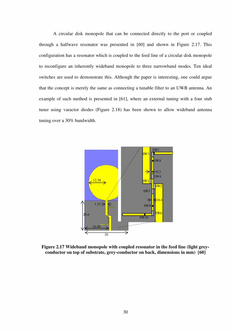
30
A circular disk monopole that can be connected directly to the port or coupled
through a halfwave resonator was presented in [60] and shown in Figure 2.17. This
configuration has a resonator which is coupled to the feed line of a circular disk monopole
to reconfigure an inherently wideband monopole to three narrowband modes. Ten ideal
switches are used to demonstrate this. Although the paper is interesting, one could argue
that the concept is merely the same as connecting a tunable filter to an UWB antenna. An
example of such method is presented in [61], where an external tuning with a four stub
tuner using varactor diodes (Figure 2.18) has been shown to allow wideband antenna
tuning over a 30% bandwidth.
Figure 2.17 Wideband monopole with coupled resonator in the feed line (light grey-
conductor on top of substrate, grey-conductor on back, dimensions in mm) [60]

31
Figure 2.18 RF impedance tuner [61]
Other antennas that have been proposed for cognitive radio systems include an L-
shaped slot antenna [62] where wideband-narrowband reconfiguration has been achieved
by using microelectromechanical switches. The switchable quad-band antenna described in
[6] used four ports to achieve four different bands and in [63] a switched wideband-dual
band antenna has been described.
2.3.3 Wideband to notch band reconfiguration
A combined wideband and narrowband antenna using separate excitation ports has
an advantage for systems that need two modes (wideband and narrowband) to
communicate simultaneously. In this type, the challenge is to provide good isolation
between ports. For a system that just requires one mode at one time, single port wide to
narrowband reconfiguration can be used. Multiple communications can also be supported
in the wideband mode, however it may suffer from adjacent channel interference. In this
condition, alternatively, a wideband mode with a notch band capability could be useful.
Work on this will now be reviewed in this section.
32
Work on the integration of wideband antennas with integrated fixed band
interference rejection filters hence, increasing the system versatility, has appeared in the
literature [64-67]. Work on fixed band notching of a Vivaldi antenna has also been
reported in [39] and [38]. In [39] a U-shaped slot was employed to notch out the 5.1 – 5.8
GHz WLAN band while in [38] a quarter wavelength short stub was inserted into a
radiating region to cut-off the 5.05-5.93 GHz band. The structure is shown in Figure 2.8.
Considering the future wireless applications, such as cognitive radio, achieving a
reconfigurable band notch operation could make an important contribution to the reduction
in the level of interference reaching the RF front end [9]. Reconfiguring the notch band is
useful for systems where the possibility of interference between users has been recognized
as an expected issue causing degradation of the performance. Some work on
reconfigurable band notch operation has been reported recently. Switched band notch
operation can be obtained using switches such as PIN diode or MEMS switches as
described in [68-70]. In [68], a CPW-fed wideband slot bow-tie, etched with a rectangular
slot, is proposed and is shown in Figure 2.19. The antenna provides wide band rejection
and is switched using PIN diode switches. Creating a slot within the radiator element will
usually change or disturb the current properties either in a pass band region or in a stop
band. Therefore, changing the electrical length of the slot will change the pass band
performance accordingly. The method proposed here creates a reasonably wide band-
notch that covers more than 1 GHz. Because the band rejection is wide, the three states can
cover approximately 2 – 4.5 GHz. The band notches were switched off by shifting them
out of band.

33
Figure 2.19 Integrated rectangular slot and wideband slot bow-tie [68]
In [69], the proposed antenna also has an on and off narrow band rejection
functionality, using MEMS switches to connect and disconnect the stub into the radiator as
shown in Figure 2.20a. However the band notch is fixed at one particular frequency. The
switching on and off of the band rejection has also been proposed in [70] where a parasitic
patch is added in the back of the rectangular monopole to obtain the band notch, as shown
in Figure 2.20b.
(a)

34
(b)
Figure 2.20 (a) Circular monopole with switchable stubs [69] and (b) Rectangular
monopole with parasitic patch at the back (left-front view, right- rear view) [70]
A tunable band notch is usually achieved by using varactors as in [71-74]. In [71] a
square ring slot is etched in a planar monopole to create band rejections. The monopole is
perpendicular to the ground plane as shown in Figure 2.21. A varactor diode is used to
obtain a tunable band rejection capability from 5.2 – 5.8 GHz.
Figure 2.21 Planar wideband monopole perpendicular to ground plane (black-
conductor, white-non conductor, light grey-bias line at the back) [71]

35
In [72], a short circuited quarter wavelength stub with a varactor is applied to a
wideband planar monopole as shown in Figure 2.22. A tuning range from 4.6 – 6.5 GHz
was achieved using two varactors.
Figure 2.22 Planar monopole with short circuited microstrip stub [72]
In [73], a pyramidal monopole with slots in each face, as shown in Figure 2.23a,
provides 4.8 – 7.47 GHz tunable band rejection with four varactors. In [74] a planar
monopole as shown in Figure 2.23b used two slots, to demonstrate dual band notches. One
capacitor is used in each slot to tune the corresponding band notch.
Figure 2.23 (a) Pyramidal monopole with four slots [73], (b) Planar monopole with
two slot [74]

36
These antennas are only capable to tune the notch band over a limited range and the
possibilities for a very wide tuning range are limited. In this thesis, an antenna with a notch
capable of a 3.5:1 tuning ratio, or 2 – 7 GHz tuning range is proposed [75]. Table 2.2
compares the performance of the tunable notch antennas reviewed in this section [71-74]
with that of the new configuration proposed in this thesis [75].
Table 2.2 Tunable band notch antenna
Antenna Band notch
technique
Number of
Varactor
Rejection
tuning ratio
Gain
suppresion, dB
[71] 1-slot ring 1 1.11:1 7.5
(with varactors)
[72] λ/4 short circuit
microstrip line
2 1.41:1 -
[73] 4 – oval slot ring 4 1.56:1 10
(with fixed
capacitors)
[74] 2- U slot shaped 2 1.26:1 (approx) 8
(with fixed
capacitors)
[75] λ/2 open circuit
microstrip line
3
(in series)
3.5:1 7 – 14
(with fixed
capacitors)
2.3.4 Wideband to wideband reconfiguration
Other concepts show wideband to wideband reconfiguration as presented in [76],
where a wideband reconfigurable rolled planar monopole antenna demonstrated a shift in
the resonant frequency by adjusting the degree of spiral tightness. The reconfiguration
shows different and multiple 10-dB return loss bandwidth as opposed to a single
narrowband operation. Figure 2.24 shows the antenna structure.
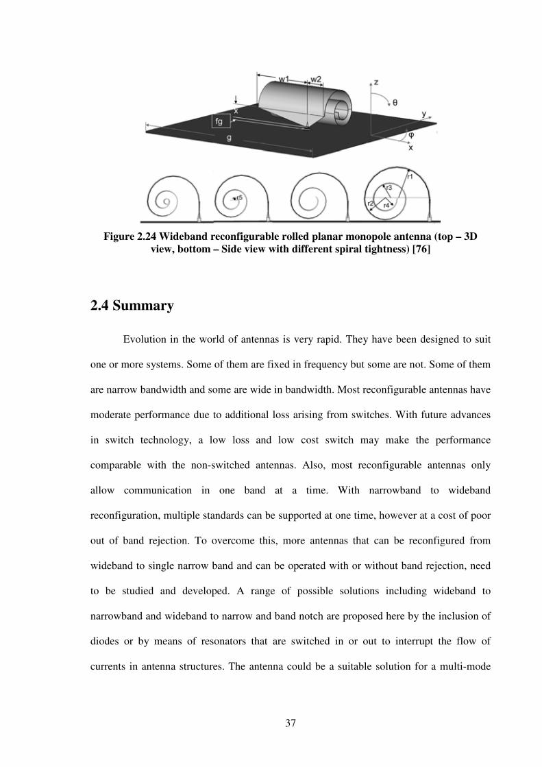
37
Figure 2.24 Wideband reconfigurable rolled planar monopole antenna (top – 3D
view, bottom – Side view with different spiral tightness) [76]
2.4 Summary
Evolution in the world of antennas is very rapid. They have been designed to suit
one or more systems. Some of them are fixed in frequency but some are not. Some of them
are narrow bandwidth and some are wide in bandwidth. Most reconfigurable antennas have
moderate performance due to additional loss arising from switches. With future advances
in switch technology, a low loss and low cost switch may make the performance
comparable with the non-switched antennas. Also, most reconfigurable antennas only
allow communication in one band at a time. With narrowband to wideband
reconfiguration, multiple standards can be supported at one time, however at a cost of poor
out of band rejection. To overcome this, more antennas that can be reconfigured from
wideband to single narrow band and can be operated with or without band rejection, need
to be studied and developed. A range of possible solutions including wideband to
narrowband and wideband to narrow and band notch are proposed here by the inclusion of
diodes or by means of resonators that are switched in or out to interrupt the flow of
currents in antenna structures. The antenna could be a suitable solution for a multi-mode

38
application requiring wideband and frequency reconfigurable antennas, such as in
cognitive radio and military applications. Two types of antennas are chosen, namely a log
periodic patch array and a Vivaldi antenna, as candidates to demonstrate wide to
reconfigured narrowband operation which are potentially useful for fixed CR radio systems
where a reasonably high gain antenna is needed for sensing purposes. From the literature
shown in this chapter, no attempt yet has been reported to reconfigure wide to narrowband
using a log periodic patch array. Also no attempt has been reported to reconfigure wide to
narrowband or tunable band rejection using a Vivaldi antenna. This will now be described
in the five following chapters.

39
CHAPTER 3
RECONFIGURABLE LOG PERIODIC APERTURE
COUPLED PATCH ARRAY
3.1 Introduction
Log-periodic antennas have multiple elements, which are scaled in a log-periodic
fashion. Using this property, and by inserting switches, a frequency reconfigurable log
periodic antenna is proposed. Recently, work on reconfigurable log periodic antennas has
been reported. In the log periodic dipole array described in [18], ideal switches are used to
control each pair of dipole arms of the antenna. This can switch from a wideband of
1 – 3 GHz, to several narrow bands. Similar work on this has also been reported in [25,
26]. As opposed to wideband to narrowband reconfiguration, work in [27-29] demonstrates
band notch method for log periodic antennas. In this chapter a novel log periodic antenna
with added switched band functionality to operate in a wideband or narrowband mode is
presented. The antenna is based on the log periodic monopole array [19], but the monopole
is replaced by a patch with an aperture coupled feed which makes the proposed antenna
very low profile yet has the added functionality to reconfigure into a narrow band mode.

40
The patch arrangement is similar to that of the uniform series feed aperture coupled leaky
wave antenna presented in [77]. The antenna reconfiguration is realized by inserting
switches into the slot aperture of the structure. A wide bandwidth mode demonstrated from
7.0 – 10 GHz and three narrowband modes at 7.1, 8.2 and 9.4 GHz can be selected. A
prototype with ideal switches has been developed. Measured results show good
performance of the proposed designs. Section 3.2 discusses the advantages in choosing an
aperture coupled log periodic patch array as a candidate for reconfiguration. Section 3.3
and 3.4 discuss the problem of the structural stop band and the procedure for eliminating it.
The effect of the scaling factor and element bandwidth are explained in section 3.5. The
fabricated antenna is discussed in section 3.6. Finally the results are presented in section
3.7 and 3.8, followed by summary in section 3.9.
3.2 Motivation
The criteria defining the best reconfigurable design, such as the number of switches
used to reconfigure the structure and the design simplicity, are investigated here. For that
purpose, the structure of the log periodic printed dipole, an electromagnetic coupled patch
array and an aperture coupled patch array are compared. Potentially, the aperture coupled
log periodic patch array (LPA) is a good candidate. The configuration allows each
radiating element to be controlled using one switch, thus, offering fewer switches
compared to a log periodic printed dipole [18]. This thus reduces the problems of biasing
many switches. In addition, because each patch is coupled to the feed line through a slot
aperture in a ground plane, switching on or off the radiating element can be achieved
relatively easyly by allowing a single switch to be placed at the centre of the aperture. On
the other hand, an electromagnetic coupled structure such as that reported by [21] will be

41
very hard to switch because there is no specific coupling mediator between the patch and
the feed line, like the slot aperture as proposed here. Furthermore, biasing for the switches
can be located within the ground plane and therefore coupling to radiation will be small. In
this chapter the design of a wideband log periodic aperture coupled microstrip antenna and
its reconfigurable version is proposed. Because of the structure size, the proposed antenna
is designed to operate from 7 – 10 GHz. A wider bandwidth can be obtained but with more
elements and bigger in size. A nearly omnidirectional pattern could be achievable by
placing a set of LPA’s around a tapered shape cylinder where each of the LPA’s has a
beam in forward fire direction. To feed a circular array in order to get a nearly
omnidirectional pattern, one can use a ‘1 to N’ power splitter, where N is the number of
power splitter output ports, each output port being connected to an LPA. The number of
LPA’s will determine how smooth or rippled the omni pattern will be. The tapered
cylindrical shape is shown in Figure 3.1. It can be seen that the patches are log periodically
distributed around the cylinder, where Dn-1 = τ(Dn), and τ is the expansion factor. This
arrangement may not be possible if made on a straight shaped cylinder. Figure 3.2 explains
this.
Figure 3.1 LPA arrangement on the taper shaped cylinder

42
Figure 3.2 LPA arrangement on the straight shaped cylinder
3.3 Structural Stop Band
To achieve a broadside direction, the feeding phase should be either set to 00 or
3600. The physical spacing between adjacent elements can be of any value but should be
less than one wavelength to avoid grating lobes [20]. The simulation results however show
that high VSWR occurs when the phasing is one wavelength between elements in the log
periodic aperture coupled patch array. This can be explained as in Figure 3.3, showing a
transmission line loaded with patches. Generally, each patch creates a small mismatch in
the line. Therefore if phasing of 00 or 360
0 between each element is employed, the
reflections will add up in phase and thus poor input return loss will result.
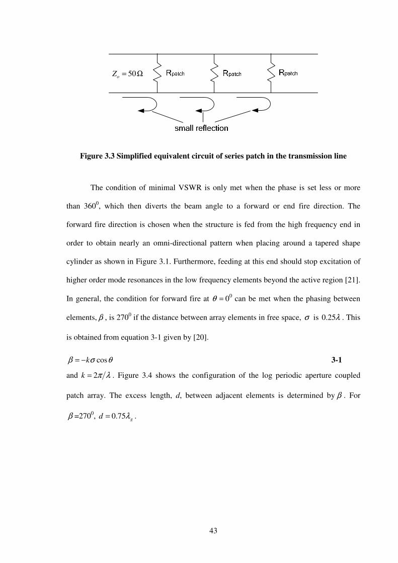
43
Ω= 50oZ
Figure 3.3 Simplified equivalent circuit of series patch in the transmission line
The condition of minimal VSWR is only met when the phase is set less or more
than 3600, which then diverts the beam angle to a forward or end fire direction. The
forward fire direction is chosen when the structure is fed from the high frequency end in
order to obtain nearly an omni-directional pattern when placing around a tapered shape
cylinder as shown in Figure 3.1. Furthermore, feeding at this end should stop excitation of
higher order mode resonances in the low frequency elements beyond the active region [21].
In general, the condition for forward fire at =θ 00 can be met when the phasing between
elements, β , is 2700 if the distance between array elements in free space, σ is λ25.0 . This
is obtained from equation 3-1 given by [20].
θσβ cosk−= 3-1
and λπ2=k . Figure 3.4 shows the configuration of the log periodic aperture coupled
patch array. The excess length, d, between adjacent elements is determined by β . For
β =2700, gd λ75.0= .
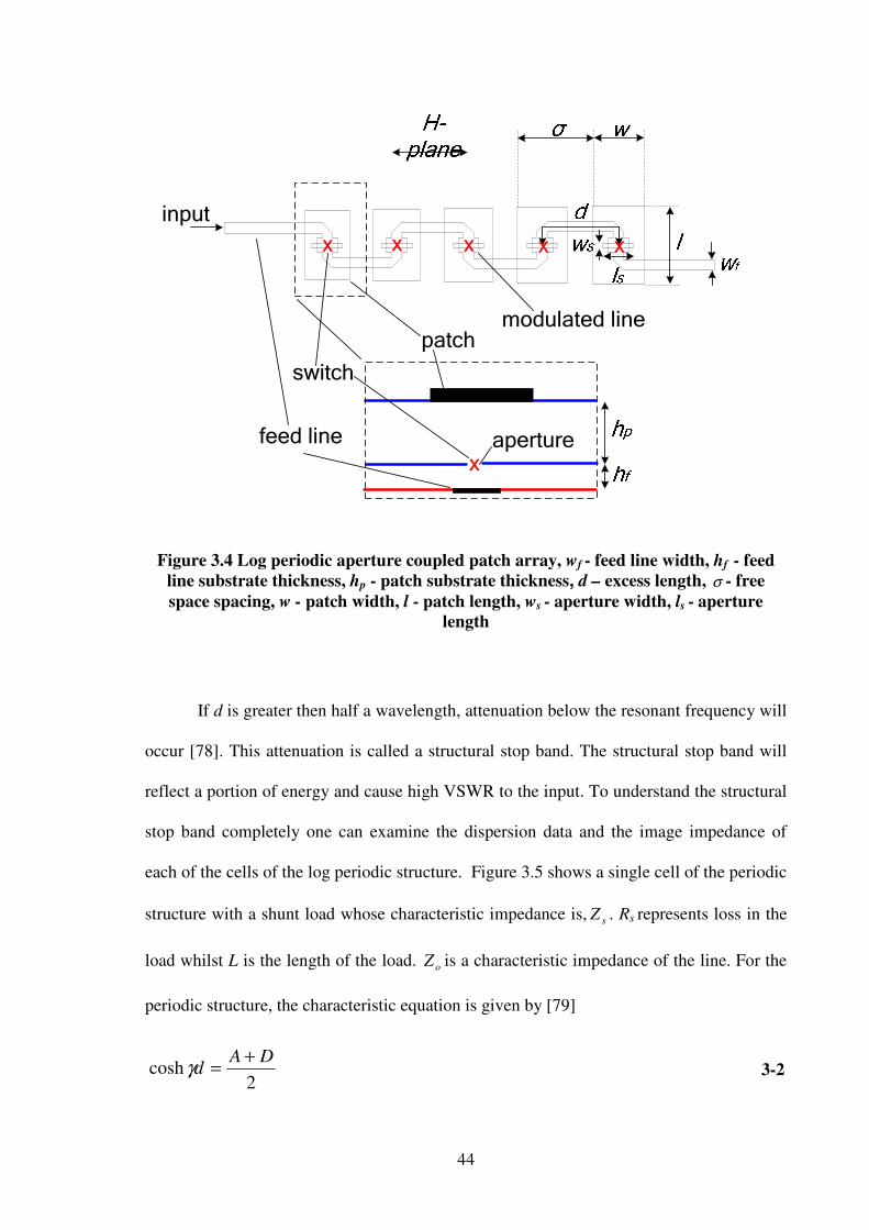
44
input
patch
feed line
modulated line
aperturex
switch
x x x x x
Figure 3.4 Log periodic aperture coupled patch array, wf - feed line width, hf - feed
line substrate thickness, hp - patch substrate thickness, d – excess length, σ - free
space spacing, w - patch width, l - patch length, ws - aperture width, ls - aperture
length
If d is greater then half a wavelength, attenuation below the resonant frequency will
occur [78]. This attenuation is called a structural stop band. The structural stop band will
reflect a portion of energy and cause high VSWR to the input. To understand the structural
stop band completely one can examine the dispersion data and the image impedance of
each of the cells of the log periodic structure. Figure 3.5 shows a single cell of the periodic
structure with a shunt load whose characteristic impedance is, sZ . Rs represents loss in the
load whilst L is the length of the load. oZ is a characteristic impedance of the line. For the
periodic structure, the characteristic equation is given by [79]
2cosh
DAd
+=γ 3-2

45
where djbad )( +=γ and A and D are parameters of the ABCD matrix for the cell.
Strong attenuation, ad, occurs when bd = 00 or 180
0 where |
2|cosh 1 DA
ad+
= −. For a
symmetric cell, the image impedance is given by [79]
C
BZ i = 3-3
Figure 3.5 Single cell with a shunt load of periodic structure
The shunt load sY is given by [78]
kLjZRY
ss
scot
1
−= 3-4
and
kdZY
jkdA os sin2
cos += 3-5
( )
−+= kd
ZYjkdjZB os
o cos12
sin 3-6
( )
+−= kd
ZYjkdjYC os
o cos12
sin 3-7
kdZY
jkdD os sin2
cos += 3-8
For a case (case 1) where d is a quarter of the guided wavelength, it is observed that the
image impedance calculated from equation 3.3, 3.6 and 3.7 does not vary much from 50 Ω
below the resonant frequency (see Figure 3.6a). The concept of “image impedance” is

46
explained in reference [79]. It is the impedance that occurs when the section is embedded
in an infinite line of similar sections. In other word it can also be defined as the terminating
impedance on the output port which leads to an input impedance that has the same value.
An attenuation owing to radiation, copper and dielectric loss can be seen in Figure
3.6b. This attenuation occurs when bd reaches 1800 (see Figure 3.6c). However for a case
(case 2) where excess length is used (i.e d ≥ half of the guided wavelength) the image
impedance varies from 50 Ω and the structural stop band exists because bd reaches 1800
before resonance (see Figure 3.7). When feeding from the high frequency end, energy goes
to the resonant region and is mostly radiated. Beyond that there is not much energy left and
therefore the stop band at high frequency will not affect the antenna operation too much.
However the stop band below the resonant frequency is really the problem.
0 0.5 1 1.5 20
50
100
150
200
250
f/f
Zi,
oh
m
below resonant frequency
(a)

47
0 0.2 0.4 0.6 0.8 10
0.5
1
1.5
2
ad, neper
f/f
(b)
0 0.5 1 1.5 2 2.5 3 3.50
0.5
1
1.5
2
bd, radian
f/fr
pi
(c)
Figure 3.6 (a) Image impedance, Zi, (b) Attenuation, dα , (c) Phase, bd,
Case1, gd λ25.0=

48
0 0.5 1 1.5 20
50
100
150
200
250
f/f
Zi,
oh
m
(a)
0 0.2 0.4 0.6 0.8 10
0.5
1
1.5
2
ad, neper
f/f
(b)
0 0.5 1 1.5 2 2.5 3 3.50
0.5
1
1.5
2
bd, radian
f/fr
pi
Figure 3.7 (a) Image impedance, |Zi| (b) Attenuation, dα (c) Phase, bd,
Case2, gd λ75.0=

49
A cascade of single cells forming a log periodic structure loading by shunt loads
with an expansion factor, τ , is shown in Figure 3.8. If each cell has at least one structural
stop band as shown in Figure 3.7b, a limited bandwidth (<2:1) log periodic array will
result. To overcome this, the variation of image impedance must be minimal as in case 1 to
eliminate the structural stop band.
Zc
Figure 3.8 A cascaded single cells forming a log periodic structure
3.4 Eliminating Structural Stop Band
A method suggested by [78] for minimizing the variation of image impedance is
applied here. The minimization is achieved when the impedance of the line is modulated.
Figure 3.9 shows how the line is modulated by changing the characteristic impedance on a
small part of the line. 212 5.05.0 dddd ++= as in Figure 3.9.
.
Figure 3.9 Transmission line with impedance modulation

50
An example of eliminating the structural stop band is now described. A two-port
section representing a single element of the structure is shown in Figure 3.10a. d is gλ75.0 .
The structure resonates at 9.583 GHz as shown in Figure 3.10b. Figure 3.10c shows the
calculated image impedance. It shows the image impedance is very different from 50 Ω
between 6.65 and 7.84 GHz. This causes a stop band between those frequencies, as shown
in Figure 3.10d. It occurs below the resonant frequency of 9.583 GHz. The magnitude of
the image impedance at this frequency is 31 Ω.
(a)
0 2 4 6 8 10 12-50
-40
-30
-20
-10
0
9.583 GHz
s-p
ara
me
ter,
dB
frequency, GHz
S11
S21
(b)

51
0 2 4 6 8 10 120
50
100
150
200
250
9.583 GHz,(31 Ω)
|Zi|,
Ω
frequency, GHz
(c)
0.00 0.05 0.10 0.15 0.20 0.25 0.300
2
4
6
8
10
12
fre
qu
en
cy,
GH
z
ad, neper
(d)
Figure 3.10 (a) Single cell of aperture coupled fed structure without impedance
modulation, (b) simulated S11 and S21, (c) Image impedance, |Zi|, (d) Attenuation, ad
To eliminate the stop band, the variation of image impedance has to be minimized.
This is done by modulating the impedance of the line. Figure 3.11a shows the line, where
the modulated part has a width, w and a length d1. In this example the line width, w, is set

52
according to the value of image impedance at 9.583 GHz, when the feeder is unmodulated.
d1 is then optimised until the variation of the image impedance is minimised. Figure 3.11b
shows the image impedance and Figure 3.11c shows the stop band response after the
modulation. The variation of image impedance below the resonant frequency is now small
and it is now 44.28 Ω at the resonant frequency. The attenuation plot shows ad = 0, from 0
to 12 GHz, demonstrating that no stop band occurs. This method is applied for each
element that produces a stop band within the operating frequency of 7 – 10 GHz.
(a)
0 2 4 6 8 10 120
50
100
150
200
250
9.583 GHz,(44.28 Ω)
|Zi|,
Ω
frequency, GHz
(b)

53
0.00 0.05 0.10 0.15 0.20 0.25 0.300
2
4
6
8
10
12
ad = 0
fre
qu
en
cy,
GH
z
ad,neper
(c)
Figure 3.11 (a) Single cell of aperture coupled fed structure with impedance
modulation, (b) Image impedance, |Zi|, (c) Attenuation, ad
3.5 Scaling Factor and Element Bandwidth
The first two criteria needed to design a very wideband log periodic aperture
coupled fed array have been described. A good match can only be achieved if the radiation
pattern is set to forward or backward fire, whilst a very wideband response is achieved by
employing a modulated impedance feeder, eliminating the structure stop bands. In this
section, two other criteria are further discussed.
The relation between element bandwidth and scaling factor is studied. The scaling
factor must suit the bandwidths of individual elements in order to obtain a reasonable
efficiency. Figure 3.12 shows the calculated efficiency of a ten element array with 1.03 and
1.015 expansion factors simulated on Duroid substrate.
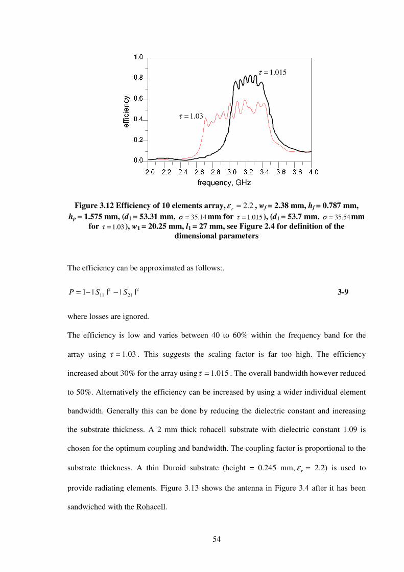
54
03.1=τ
015.1=τ
Figure 3.12 Efficiency of 10 elements array, 2.2=rε , wf = 2.38 mm, hf = 0.787 mm,
hp = 1.575 mm, (d1 = 53.31 mm, 14.35=σ mm for 015.1=τ ), (d1 = 53.7 mm, 54.35=σ mm
for 03.1=τ ), w1 = 20.25 mm, l1 = 27 mm, see Figure 2.4 for definition of the
dimensional parameters
The efficiency can be approximated as follows:.
2
21
2
11 ||||1 SSP −−= 3-9
where losses are ignored.
The efficiency is low and varies between 40 to 60% within the frequency band for the
array using 03.1=τ . This suggests the scaling factor is far too high. The efficiency
increased about 30% for the array using 015.1=τ . The overall bandwidth however reduced
to 50%. Alternatively the efficiency can be increased by using a wider individual element
bandwidth. Generally this can be done by reducing the dielectric constant and increasing
the substrate thickness. A 2 mm thick rohacell substrate with dielectric constant 1.09 is
chosen for the optimum coupling and bandwidth. The coupling factor is proportional to the
substrate thickness. A thin Duroid substrate (height = 0.245 mm, =rε 2.2) is used to
provide radiating elements. Figure 3.13 shows the antenna in Figure 3.4 after it has been
sandwiched with the Rohacell.
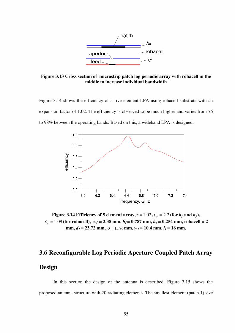
55
Figure 3.13 Cross section of microstrip patch log periodic array with rohacell in the
middle to increase individual bandwidth
Figure 3.14 shows the efficiency of a five element LPA using rohacell substrate with an
expansion factor of 1.02. The efficiency is observed to be much higher and varies from 76
to 98% between the operating bands. Based on this, a wideband LPA is designed.
Figure 3.14 Efficiency of 5 element array, 02.1=τ , 2.2=rε (for hf and hp),
09.1=rε (for rohacell), wf = 2.38 mm, hf = 0.787 mm, hp = 0.254 mm, rohacell = 2
mm, d1 = 23.72 mm, 86.15=σ mm, w1 = 10.4 mm, l1 = 16 mm,
3.6 Reconfigurable Log Periodic Aperture Coupled Patch Array
Design
In this section the design of the antenna is described. Figure 3.15 shows the
proposed antenna structure with 20 radiating elements. The smallest element (patch 1) size

56
is w1 = 7 mm and l1 = 10.77 mm. The expansion factor of 1.02 is used. The patches are
printed on a 0.254 mm thick Duroid 5880 substrate with the dielectric constant of 2.2. The
meandered 50 Ω feed line and slot apertures are etched on a similar 0.787 mm thick
substrate. The array is terminated with a matched load at the end of the line to prevent
reflections. Each aperture is spaced a quarter wavelength apart and fed with 2700 phasing
thus giving a forward fire radiation pattern. A single switch, denoted as ‘x’ in Figure 3.15b
and Figure 3.15c, is placed at the centre of each aperture. Rohacell foam with a dielectric
constant of 1.09 and thickness of 2 mm is sandwiched between the patch and feed
substrates. The patch configuration is arranged in the H-plane axis. The feed line is
enclosed with a screening box size of hb x lb. This is important to reduce back radiation.
The box size (hb is 4.18 mm and lb is 12.7 mm) is designed so that the cut off frequency is
at 11.8 GHz which is above the top end operating band of 10 GHz. In the simulation, metal
pads, of size 1 mm x 1 mm, have been used to approximate switching devices. The
presence of the metal pad represents the switch on state and their absence represents the off
state. This is believed acceptable and suitable to demonstrate the basic switching concept.
For a twenty element LPA, twenty switches are employed. Wideband operation is achieved
when all the switches are in off states thus making the antenna act as a normal log periodic
antenna. To provide narrow band operation, such as high band mode, the four most high
frequency slots were kept open. The rest of the slots are closed by bridging them with the
switches. The other sub bands are achieved by bridging a group of slots of the antenna as
shown in Table 3.1. The design has been simulated by CST simulation software. The
boundary has been set to open add space and the port used in the model is a waveguide
port. All details of the box, excluding the screw as seen in the photograph of Figure 3.15
for clamping the box, were included in the simulation. Details of box dimensions are
presented in Appendix E.

57
patch1
input
matched
load
H-plane
m=50 mm
x
z
y
n=280 mm
patch20
screws
(a)
(b)
(c)
Figure 3.15 Proposed antenna structure (a) Perspective view (b) Side view (c) Top
view, 02.1=τ , 2.2=rε (for hf and hp), 09.1=rε (for rohacell), wf = 2.38 mm,
hf = 0.787 mm, hp = 0.254 mm, rohacell = 2 mm, d1 = 16.1 mm, 86.15=σ mm,
w1 = 7 mm, l1 = 10.77 mm,

58
Table 3.1 Switches location
No of Slot Wide band High band Mid band Low band
1 o o x x
2 o o x x
3 o o x x
4 o o x x
5 o x x x
6 o x x x
7 o x x x
8 o x o x
9 o x o x
10 o x o x
11 o x o x
12 o x o x
13 o x o x
14 o x x x
15 o x x x
16 o x x o
17 o x x o
18 o x x o
19 o x x o
20 o x x o
o-, OFF states (open); x-, ON states (closed)
3.7 Simulation Results
In this section, simulation results are first presented to demonstrate the concepts.
The simulated wideband mode scattering parameters and the simulated efficiency are
shown in Figure 3.16a and Figure 3.16b. The antenna operates over a frequency range of 7
to 10 GHz with efficiency ranging from 70 to 95%. Figure 3.17 shows the effects on the
radiation patterns with and without the screening box. There is strong back radiation from
the feed line in Figure 3.17a when the screening box is absent. The back radiation is
effectively reduced as in Figure 3.17b after the screening box is in place. Figure 3.18

59
shows the simulated radiation pattern in wideband mode. The pattern is forward fire of 600
at 7.1GHz, 550 at 8.2 GHz and 50
0 at 9.4 GHz.
6 7 8 9 10-35
-30
-25
-20
-15
-10
-5
0
s-p
ara
me
ter,
dB
frequency, GHz
|S11
|
|S21
|
(a)
6.0 6.5 7.0 7.5 8.0 8.5 9.0 9.5 10.00.1
0.2
0.3
0.4
0.5
0.6
0.7
0.8
0.9
1.0
eff
icie
ncy
frequency, GHz
(b)
Figure 3.16 Simulated wideband mode, (a) scattering parameters (b) efficiency
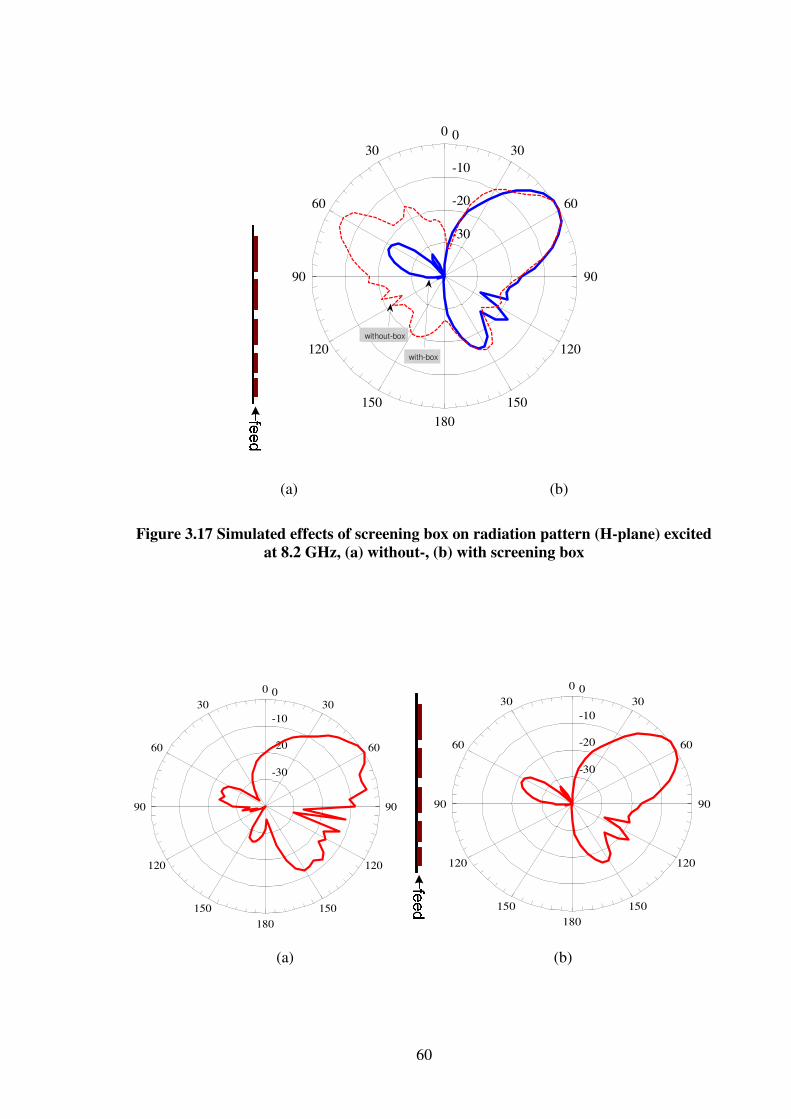
60
-30
-20
-10
0
60
120
30
150
0
180
30
150
60
120
90 90
without-box
with-box
(a) (b)
Figure 3.17 Simulated effects of screening box on radiation pattern (H-plane) excited
at 8.2 GHz, (a) without-, (b) with screening box
(a) (b)
-30
-20
-10
0
60
120
30
150
0
180
30
150
60
120
90 90
-30
-20
-10
0
60
120
30
150
0
180
30
150
60
120
90 90
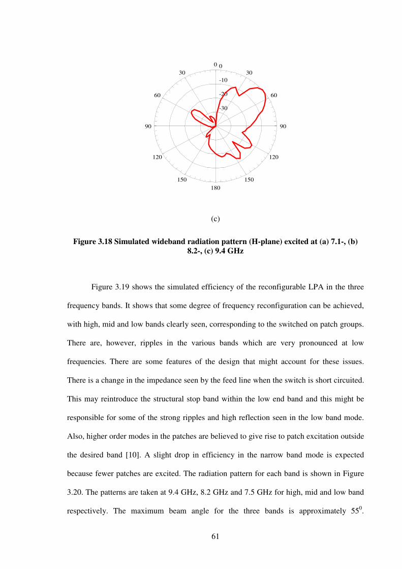
61
(c)
Figure 3.18 Simulated wideband radiation pattern (H-plane) excited at (a) 7.1-, (b)
8.2-, (c) 9.4 GHz
Figure 3.19 shows the simulated efficiency of the reconfigurable LPA in the three
frequency bands. It shows that some degree of frequency reconfiguration can be achieved,
with high, mid and low bands clearly seen, corresponding to the switched on patch groups.
There are, however, ripples in the various bands which are very pronounced at low
frequencies. There are some features of the design that might account for these issues.
There is a change in the impedance seen by the feed line when the switch is short circuited.
This may reintroduce the structural stop band within the low end band and this might be
responsible for some of the strong ripples and high reflection seen in the low band mode.
Also, higher order modes in the patches are believed to give rise to patch excitation outside
the desired band [10]. A slight drop in efficiency in the narrow band mode is expected
because fewer patches are excited. The radiation pattern for each band is shown in Figure
3.20. The patterns are taken at 9.4 GHz, 8.2 GHz and 7.5 GHz for high, mid and low band
respectively. The maximum beam angle for the three bands is approximately 550.
-30
-20
-10
0
60
120
30
150
0
180
30
150
60
120
90 90
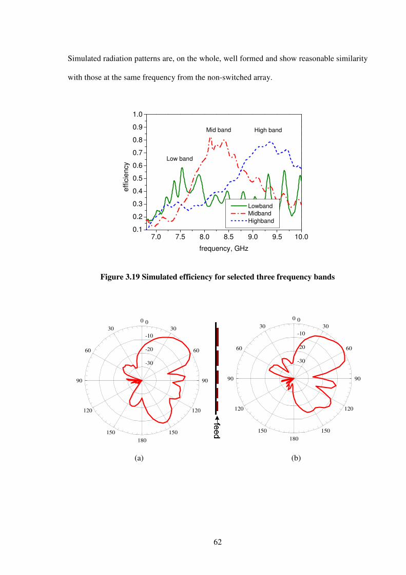
62
Simulated radiation patterns are, on the whole, well formed and show reasonable similarity
with those at the same frequency from the non-switched array.
7.0 7.5 8.0 8.5 9.0 9.5 10.00.1
0.2
0.3
0.4
0.5
0.6
0.7
0.8
0.9
1.0
High bandMid band
Low band
eff
icie
ncy
frequency, GHz
Lowband
Midband
Highband
Figure 3.19 Simulated efficiency for selected three frequency bands
(a) (b)
-30
-20
-10
0
60
120
30
150
0
180
30
150
60
120
90 90
-30
-20
-10
0
60
120
30
150
0
180
30
150
60
120
90 90

63
(c)
Figure 3.20 Simulated radiation pattern (H-plane) for selected three frequency bands
(a) Low -, (b) Mid- and (c) High band
3.7.1 Improving Low Band Performances
When the high frequency slot is short circuited, there will be a change in the
impedance seen by the feed line. This will upset the image impedance and will again
introduce the structural stop band and resulting high reflection in low band mode. To
compensate for the change, the impedance of the modulated line is modified. Figure 3.21
shows the modulated impedance line and its pi equivalent circuit. Figure 3.22a shows the
structure when the slot is short circuited with Sa switch. As a convenient first
approximation, the inductor in the equivalent circuit can be assumed zero as shown in
Figure 3.22b. This can be explained as the current path, i is shorten when the slot is
bridged. This has changed the image impedance and produces a structural stop band.
-30
-20
-10
0
60
120
30
150
0
180
30
150
60
120
90 90

64
(a)
INDQ
L1
C
C2
C
C1
(b)
Figure 3.21 Modulated impedance feeder and the equivalent circuits
(a)
INDQ
L1
C
C2
C
C1
(b)
Figure 3.22 Pi equivalent circuits after slot is bridged, Sa – switch on slot

65
Elimination of the structural stop band of the second cell of the 20 element array is
now described. Figure 3.23a shows the structural stop band and Figure 3.23b shows the
image impedance of the second cell after the slot is bridged as shown in Figure 3.22. To
eliminate the stop band, the modulated line is modified somewhat as shown in Figure
3.24a. Figure 3.24b shows its equivalent circuit. This modification makes the equivalent
circuit similar to that Figure 3.21b. To simplify the design process, Lm is set equal to the
aperture width and therefore by choosing the Wm appropriately, the variation of image
impedance can be minimised and the structural stop band will be eliminated. In this
example, the structural stop band is zero when Lm is 0.8 mm and Wm is 1 mm. Figure 3.25
shows an image impedance and a structural stop band of the cell when the slot is bridged
for the modified lines as in Figure 3.24. It is observed that the structural stop band is
eliminated.
(a)
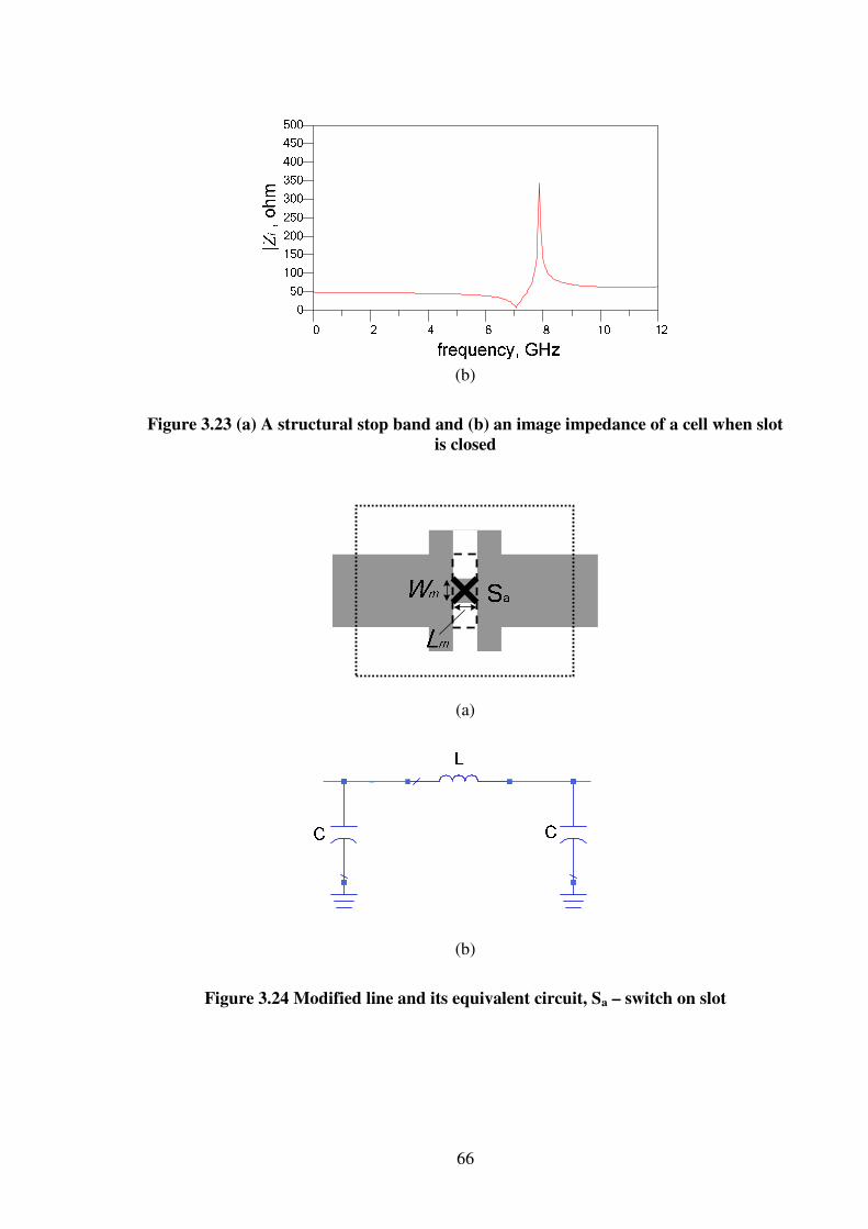
66
(b)
Figure 3.23 (a) A structural stop band and (b) an image impedance of a cell when slot
is closed
(a)
INDQ
L1
C
C2
C
C1
(b)
Figure 3.24 Modified line and its equivalent circuit, Sa – switch on slot

67
|Zi|, ohm
(a)
(b)
Figure 3.25 (a) An image impedance and, (b) a structural stop band for the modified
lines of cell 19th
after slot is closed
The improvement of low band mode efficiency is shown in Figure 3.26. To
maintain the performance of the other band, two Sf switches are added to the line as shown
in Figure 3.27. The Sf switches are open when the Sa switch is closed to improve low band
mode efficiency. On the other hand, the Sf switches are closed when the Sa switch is open,
to keep reasonably similar performances in the other mode. Simulated wideband efficiency
with the Sf and Sa switches present is shown in Figure 3.28. The wideband performance is
approximately similar in both cases. The selected three narrow band modes shown in

68
Figure 3.29 verify that the proposed concepts of reconfigurable log periodic patch array
can be achieved.
7.0 7.5 8.0 8.5 9.0 9.5 10.00.1
0.2
0.3
0.4
0.5
0.6
0.7
0.8
0.9
1.0
e
ffic
ien
cy
frequency, GHz
Lowband
Improved Lowband
Figure 3.26 Simulated low band mode efficiency before and after improvement
Figure 3.27 Switch position, Sf – switch on feed, Sa – switch on slot

69
7.0 7.5 8.0 8.5 9.0 9.5 10.00.1
0.2
0.3
0.4
0.5
0.6
0.7
0.8
0.9
1.0
eff
icie
ncy
frequency, GHz
Normal modulated line
Modified modulated line
Figure 3.28 Simulated wideband efficiency before and after improvement of low band
mode
7.0 7.5 8.0 8.5 9.0 9.5 10.00.1
0.2
0.3
0.4
0.5
0.6
0.7
0.8
0.9
1.0
Low band Mid band High band
eff
icie
ncy
frequency, GHz
Lowband
Midband
Highband
Figure 3.29 Three selected narrow band of the proposed reconfigurable log periodic
patch array

70
3.8 Measurement result
The measured wideband mode scattering parameters are shown in Figure 3.30. The
measured and simulated efficiency is presented in Figure 3.31. The antenna operates over a
frequency range of 7 to 10 GHz with efficiency ranging from 80-95%. Good agreement is
achieved although there are small differences. At some frequencies the measured
efficiency is higher than simulated. This may be accounted for by improper shielding
between hf substrate and the box. Leakage from the gap between the ground plane and the
box was found to be a significant problem which was solved by improving the electrical
connection between the two. In the simulation, no leakage occurs.
6.0 6.5 7.0 7.5 8.0 8.5 9.0 9.5 10.0-50
-40
-30
-20
-10
0
s-p
ara
me
ter,
dB
frequency, GHz
|S11
|
|S21
|
Figure 3.30 Measured wideband mode scattering parameters

71
7.0 7.5 8.0 8.5 9.0 9.5 10.00.1
0.2
0.3
0.4
0.5
0.6
0.7
0.8
0.9
1.0
eff
icie
ncy
frequency, GHz
Sim
Meas
Figure 3.31 Wideband mode efficiency
Figure 3.32 shows the measured and simulated efficiency of the reconfigurable
LPA for each selected three frequency bands. It shows that a good agreement is achieved,
with the three bands clearly seen, corresponding to the switched on patch groups. In Figure
3.32b (mid band mode) the measured efficiency in the high band is higher than the
simulated efficiency, suggesting that less rejection is being achieved. Similarly, in Figure
3.32c (low band mode), the measured efficiency in mid and high bands is higher than in
the simulation, again suggesting reduced rejection. This may be accounted for by improper
shielding between hf substrate and the box. Leakage from the gap between the ground
plane and the box was found to be a significant problem which was solved by improving
the electrical connection between the two. Figure 3.33 shows a better rejection out of band
is achieved if the copper tape is soldered to the substrate and the box as shown in Figure
3.34. Figure 3.35 shows the measured efficiency of the three narrowband modes of the
proposed reconfigurable log periodic patch array.

72
7.0 7.5 8.0 8.5 9.0 9.5 10.00.1
0.2
0.3
0.4
0.5
0.6
0.7
0.8
0.9
1.0
eff
icie
ncy
frequency, GHz
Sim
Meas
(a)
7.0 7.5 8.0 8.5 9.0 9.5 10.00.1
0.2
0.3
0.4
0.5
0.6
0.7
0.8
0.9
1.0
eff
icie
ncy
frequency, GHz
Sim
Meas
(b)

73
7.0 7.5 8.0 8.5 9.0 9.5 10.00.1
0.2
0.3
0.4
0.5
0.6
0.7
0.8
0.9
1.0
eff
icie
ncy
frequency, GHz
Sim
Meas
(c)
Figure 3.32 The selected three narrowband mode, (a) High band, (b) Mid band, and
(c) Low band
7.0 7.5 8.0 8.5 9.0 9.5 10.00.1
0.2
0.3
0.4
0.5
0.6
0.7
0.8
0.9
1.0
rejection difference
eff
icie
ncy
frequency, GHz
Glued copper tape
Soldered copper tape
Figure 3.33 Out of band rejection in mid band mode

74
Figure 3.34 Proposed screening box where a copper tape is used to reasonably enclose
the lower substrate, hf into the shielding box
7.0 7.5 8.0 8.5 9.0 9.50.1
0.2
0.3
0.4
0.5
0.6
0.7
0.8
0.9
1.0
Low band Mid band High band
eff
icie
ncy
frequency, GHz
Lowband
Midband
Highband
Figure 3.35 Measured efficiency of the reconfigurable log periodic patch array
The modification of the line to improve low band performance shows minimal
effect on the other bands. An example of wideband performance with and without line
modification is shown in Figure 3.36.
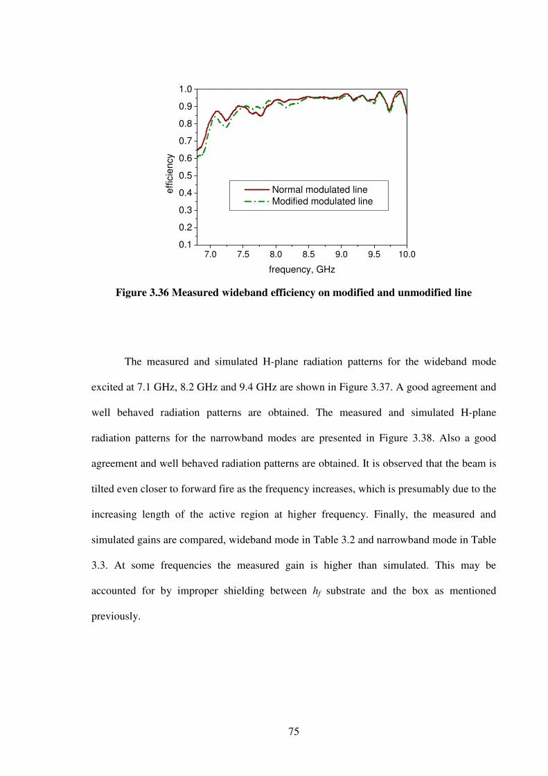
75
7.0 7.5 8.0 8.5 9.0 9.5 10.00.1
0.2
0.3
0.4
0.5
0.6
0.7
0.8
0.9
1.0
eff
icie
ncy
frequency, GHz
Normal modulated line
Modified modulated line
Figure 3.36 Measured wideband efficiency on modified and unmodified line
The measured and simulated H-plane radiation patterns for the wideband mode
excited at 7.1 GHz, 8.2 GHz and 9.4 GHz are shown in Figure 3.37. A good agreement and
well behaved radiation patterns are obtained. The measured and simulated H-plane
radiation patterns for the narrowband modes are presented in Figure 3.38. Also a good
agreement and well behaved radiation patterns are obtained. It is observed that the beam is
tilted even closer to forward fire as the frequency increases, which is presumably due to the
increasing length of the active region at higher frequency. Finally, the measured and
simulated gains are compared, wideband mode in Table 3.2 and narrowband mode in Table
3.3. At some frequencies the measured gain is higher than simulated. This may be
accounted for by improper shielding between hf substrate and the box as mentioned
previously.

76
(a)
(b)
-30
-20
-10
0
60
120
30
150
0
180
30
150
60
120
90 90
-30
-20
-10
0
60
120
30
150
0
180
30
150
60
120
90 90

77
(c)
–––––– simulated, –– - –– measured
Figure 3.37 Wideband mode radiation pattern excited at (a) 7.1 GHz, (b) 8.2 GHz and
(c) 9.4 GHz
(a)
-30
-20
-10
0
60
120
30
150
0
180
30
150
60
120
90 90
-30
-20
-10
0
60
120
30
150
0
180
30
150
60
120
90 90
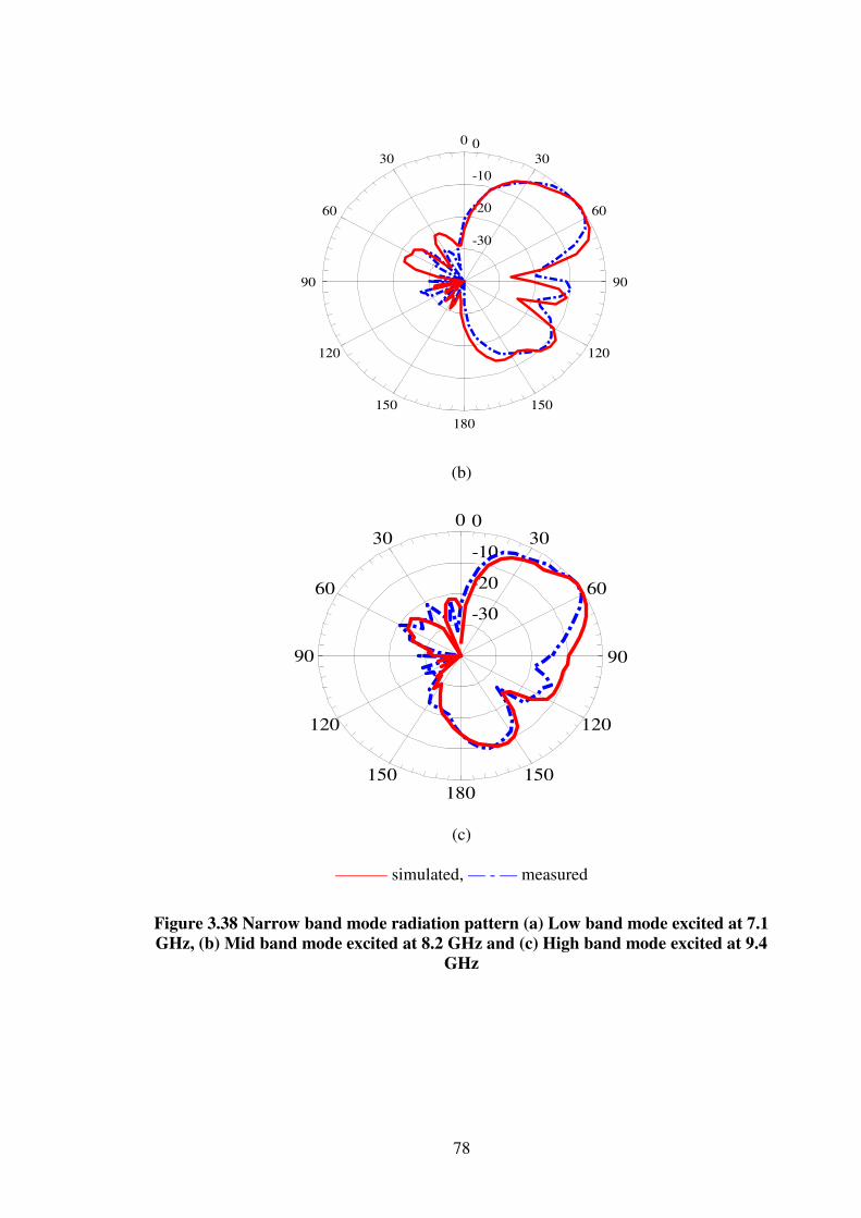
78
(b)
(c)
–––––– simulated, –– - –– measured
Figure 3.38 Narrow band mode radiation pattern (a) Low band mode excited at 7.1
GHz, (b) Mid band mode excited at 8.2 GHz and (c) High band mode excited at 9.4
GHz
-30
-20
-10
0
60
120
30
150
0
180
30
150
60
120
90 90
-30
-20
-10
0
60
120
30
150
0
180
30
150
60
120
90 90

79
Table 3.2 Gain of the proposed antenna in wideband mode
Gain, dBi 7.1 GHz 8.2 GHz 9.4 GHz
Simulated 11.64 13.60 13.08
Measured 9.83 16.42 14.54
Table 3.3 Gain of the proposed antenna in narrow band mode
Gain, dBi Low band Mid band High band
Simulated 10.91 10.74 10.61
Measured 8.08 13.69 11.56
3.9 Summary
A novel reconfigurable log periodic patch array has been proposed by inserting the
switch within the aperture slots. Three modes of reconfiguration are shown, when three
groups of patches were selected within the array. The design guideline has been derived to
allow some optimizing of the low band performances. More sub-bands could be achieved
with different patches group selection. Nevertheless, in the relatively simple example
shown, good efficiency has been obtained for each of the sub bands. The antenna is low
profile and can be easily mounted to any structure such as in the body of an aircraft.
Furthermore the bias circuit can be implemented easily in the ground plane which will help
to reduce coupling to radiation. The proposed antenna could be a suitable solution for
applications requiring wideband sensing and dynamic band switching, such as in military
applications or cognitive radio. The work described here has been published in [80, 81].
However there are some drawbacks. Ideally there should be only one single switch needed
to switch off one element, however because of the reintroduction of the stopband in the
low band mode, two extra switches are needed to improve the performance. The need for a
screening box also makes the structure more complex. Furthermore, because individual

80
elements have narrow bandwidth, a smaller scale factor is used which results in more
elements. This then will increase the complexity of the bias circuits.
Now it has been shown that for a frequency independent antenna, where radiation
occurs at different parts at different frequencies, a frequency reconfigurable antenna can be
achieved by switching off some of the radiating elements. In the next chapter, the same
general idea is applied but in a Vivaldi antenna, since they also radiate from different parts
at different frequencies.

81
CHAPTER 4
WIDE-NARROW RECONFIGURABLE BAND
MULTIPLE RING VIVALDI ANTENNA
4.1 Introduction
In this chapter, a novel switched band Vivaldi antenna is proposed. It is relatively
small, simple to manufacture (no shielding box) and less complex in biasing circuit (fewer
switches) compared to the reconfigurable log periodic patch array described in the previous
chapter. To demonstrate its functionality, the proposed antenna shows reconfiguration
between a single wideband mode (1.0 - 3.2 GHz) and three narrowband modes. Potentially,
it can be designed to cover a very wide bandwidth and can have a wide range of frequency
reconfiguration. To achieve switched band properties, eight ring slots which form filters
were inserted to the antenna. The overall operating band can be switched by coupling each
ring slot into the slot edges through the gaps controlled by means of PIN diode switches,
which stop or pass the edge current to obtain frequency reconfiguration capability. Details
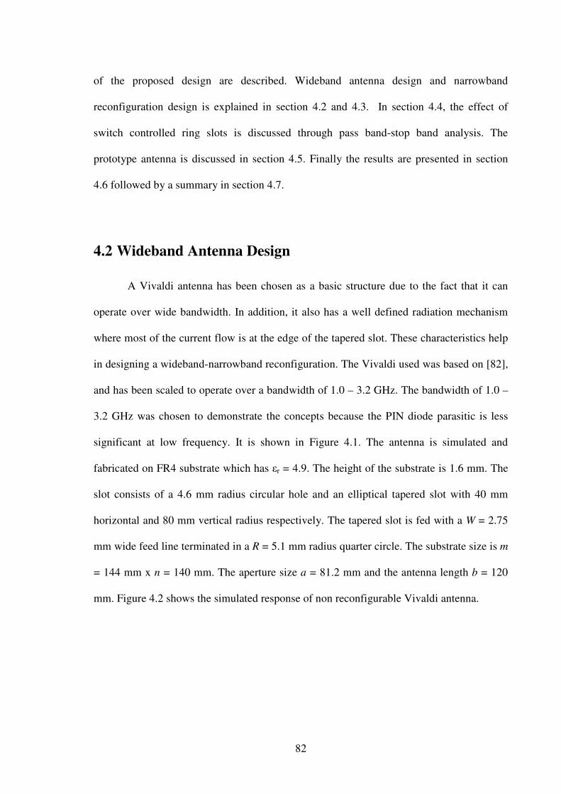
82
of the proposed design are described. Wideband antenna design and narrowband
reconfiguration design is explained in section 4.2 and 4.3. In section 4.4, the effect of
switch controlled ring slots is discussed through pass band-stop band analysis. The
prototype antenna is discussed in section 4.5. Finally the results are presented in section
4.6 followed by a summary in section 4.7.
4.2 Wideband Antenna Design
A Vivaldi antenna has been chosen as a basic structure due to the fact that it can
operate over wide bandwidth. In addition, it also has a well defined radiation mechanism
where most of the current flow is at the edge of the tapered slot. These characteristics help
in designing a wideband-narrowband reconfiguration. The Vivaldi used was based on [82],
and has been scaled to operate over a bandwidth of 1.0 – 3.2 GHz. The bandwidth of 1.0 –
3.2 GHz was chosen to demonstrate the concepts because the PIN diode parasitic is less
significant at low frequency. It is shown in Figure 4.1. The antenna is simulated and
fabricated on FR4 substrate which has εr = 4.9. The height of the substrate is 1.6 mm. The
slot consists of a 4.6 mm radius circular hole and an elliptical tapered slot with 40 mm
horizontal and 80 mm vertical radius respectively. The tapered slot is fed with a W = 2.75
mm wide feed line terminated in a R = 5.1 mm radius quarter circle. The substrate size is m
= 144 mm x n = 140 mm. The aperture size a = 81.2 mm and the antenna length b = 120
mm. Figure 4.2 shows the simulated response of non reconfigurable Vivaldi antenna.

83
(a)
(b)
Figure 4.1 Non reconfigurable Vivaldi antenna, (a) front view, (b) rear view showing
microstrip feed
0.8 1.2 1.6 2.0 2.4 2.8 3.2-40
-30
-20
-10
0
|S11|, d
B
frequency, GHz
Figure 4.2 Simulated wideband non reconfigurable Vivaldi antenna
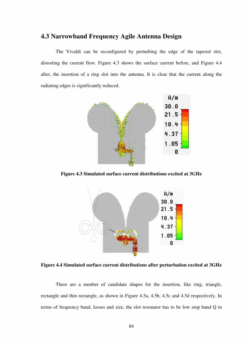
84
4.3 Narrowband Frequency Agile Antenna Design
The Vivaldi can be reconfigured by perturbing the edge of the tapered slot,
distorting the current flow. Figure 4.3 shows the surface current before, and Figure 4.4
after, the insertion of a ring slot into the antenna. It is clear that the current along the
radiating edges is significantly reduced.
Figure 4.3 Simulated surface current distributions excited at 3GHz
Figure 4.4 Simulated surface current distributions after perturbation excited at 3GHz
There are a number of candidate shapes for the insertion, like ring, triangle,
rectangle and thin rectangle, as shown in Figure 4.5a, 4.5b, 4.5c and 4.5d respectively. In
terms of frequency band, losses and size, the slot resonator has to be low stop band Q in

85
order to have wide stop band ranges, have low pass band loss and high stop band loss and
be small in size. Figure 4.6 shows the simulated admittance showing that the Q factor is
almost similar for ring, triangle and rectangle shape but slightly higher in the thin
rectangle. A similar behaviour is also observed in the insertion loss plot shown in Figure
4.7. The loss is almost similar for ring, triangle and rectangle shape but slightly lower in
the thin rectangle. In term of Q factor, ring, triangle or rectangle shapes are good
candidates. Nevertheless, the ring shape slot, Figure 4.5a, has been chosen because it’s
relatively easy to design. The Q factor of the ring slot is 1.16.
(a) (b)
(c) (d)
Figure 4.5 Slot shapes (a) ring-, (b) triangle-, (c) rectangle-, (d) thin rectangle shape

86
0.4 0.6 0.8 1.0 1.2 1.4 1.60.000
0.005
0.010
|Y|, S
frequency, f/fstop
rectangle
ring
thinrect
triangle
Figure 4.6 Simulated admittance, |Y| of various slot shapes
0.0 0.2 0.4 0.6 0.8 1.0 1.2 1.4 1.6 1.8 2.0-14
-12
-10
-8
-6
-4
-2
|S2
1|, d
B
frequency, f/fpass
rectangle
ring
thinrect
triangle
Figure 4.7 Simulated |S21| of various slot shapes
The Vivaldi can be divided into two regions, namely the propagation and active
regions. The propagation region is the area which acts like a transmission line and the
active region is the area where the signals start to radiate. The radiation occurs when the
slot width is approximately half of the wavelength, which makes each part of the Vivaldi
radiate at different frequencies. The radiation at lower frequencies occurs closer to the
wider end of the slot whilst higher frequencies occur at the narrower end. This suggests

87
that the ring slots should be placed at various positions along the tapered slot to control the
frequency performance. The way this is done is now described.
Wideband to narrowband reconfiguration can be made by integrating a switched
ring slot in the Vivaldi. For simplification purposes three narrowband modes were selected,
namely low band, mid band and high band. Ideally the frequency response of each ring slot
should be chosen depending on which narrowband configurations it is designed for. For
example a low pass filter response is used in selecting low band mode while a band pass
response can be used to select mid band mode. Figure 4.8 shows the geometry and
simulated response of the ring slots on a uniform slot line. A single ring slot produced a
stop band response while cascaded ring slots produced a pass band response. In addition,
adding bridges as shown in Figure 4.8c transformed the band stop to low pass response.
The equivalent transmission line models of the ring slot resonator are now
described. The average circumference of the single ring slot in Figure 4.9a is 52.3 mm
which is approximately a half wavelength at 2.3 GHz. The differential operation of the slot
line creates a virtual short circuit, denoted as sc, at the middle point of the structure as
shown in the figure. The short circuit transforms over a quarter wavelength to an open
circuit at the excitation point which produces a stop band at 2.3 GHz. On the other hand,
the cascaded ring slots in Figure 4.9b make the length approximately half wavelength long
at 2.2 GHz. This thus makes a short circuit at the excitation point, which produces a pass
band around 2.2 GHz. Finally, with added bridges, the ring slot shown in Figure 4.9c
becomes a very short slot, an eighth wavelength long. This transforms to a stop band at 4.6
GHz or to an inductance at a low band 1.2 GHz at the excitation point.

88
-40
-30
-20
-10
0
1 1.2 1.4 1.6 1.8 2 2.2 2.4 2.6 2.8 3 3.2
frequency, GHz|(
S21)|
, dB
(a)
-30
-20
-10
0
1 1.2 1.4 1.6 1.8 2 2.2 2.4 2.6 2.8 3 3.2
frequency, GHz
|(S
21)|
, dB
(b)
-30
-20
-10
0
1 1.2 1.4 1.6 1.8 2 2.2 2.4 2.6 2.8 3 3.2
frequency, GHz
|(S
21)|
, dB
(c)
Figure 4.8 Simulated S21 of ring slot resonator (a) band stop (b) band pass (c) low
pass; (slot line width = 2 mm, ring outer radius = 10 mm, ring inner radius = 6 mm,
small connecting gap = 4 mm x 3.48 mm, small bridge[case (c) only] = 4 mm x 2 mm)

89
4λ
2λ
8λ
(a) (b) (c)
Figure 4.9 Ring slot resonator (a) band stop (b) band pass (c) low pass
Since the Vivaldi radiates from different parts of the structure at different
frequencies, the narrower end area will become the radiating region for high frequency
signals. It is thus appropriate to locate the ring slot there, in order to get the low band
mode. Figure 4.10 shows a pair of low pass ring slots at the lower end. From the S11 it is
clear that this produces a low band response. In order to stop the low band, the top end of
the antenna has the band stop ring slot. Figure 4.11 shows the effect of ring slot radius on
the Vivaldi S11. With r =15 mm good return loss of top end band is achieved. This is
because the larger the value of r, the lower is stop-band, resulting in less perturbation of
the pass-band thus giving better S11.
0.6 1 1.4 1.8 2.2 2.6 3 3.4
frequency, GHz
-20
-15
-10
-5
0
|(S
11)|, dB
Figure 4.10 Simulated S11 of low band configurations (x = 9.55 mm)

90
1 1.5 2 2.5 3
frequency, GHz
-15
-10
-5
0
|S(1
1)|, dB
r=10 mm
r=12 mm
r=15 mm
Figure 4.11 Simulated S11 of high band configurations (x = 56.2 mm)
Mid band operation is selected by using a band pass ring slot configuration. The
position of the ring slot section has an effect on the frequency response. Figure 4.12
compares the performance for optimally and non optimally positioned 2.2 GHz ring slot
resonators. Theoretically, to minimize the perturbation of the travelling wave on the
tapered slot at the pass band frequency, the ring slot section should be positioned at a point
on the line where its image impedance, ZRS, is equal to the characteristic impedance of the
line, ZSLOT. The image impedance of a short section of line containing the ring slot
resonator (Figure 4.13) is defined as the terminating impedance on the output port (AA’)
which leads to an input impedance (at BB’) that has the same value. In Figure 4.14,
resonators causing four different pass bands have all been optimally positioned to achieve
good pass band match.
The frequency of the pass band can be selected by designing the ring slot as shown
in Figure 4.14a. If reconfiguration from a wideband to a single narrow band is required the
narrowband frequency can be chosen in this way. However there are size constraints if, as

91
in the demonstration described in this chapter, wideband and low, middle and high pass
modes are integrated together.
1 1.5 2 2.5 3
frequency, GHz
-20
-15
-10
-5
0
|(S
11)|
, d
B
(a)
1 1.5 2 2.5 3
frequency, GHz
-20
-15
-10
-5
0
|(S
11
)|, d
B
(b)
Figure 4.12 (a) Simulated antenna S11 when resonators at matched position, x = 23.69
(b) resonators at x = 43.77 mm

92
Figure 4.13 Impedances associated in finding optimum ring slot position, ideal
condition when ZRS = ZSLOT
x1
RS1
x3
RS3x4
RS4
x2
RS2
(a)
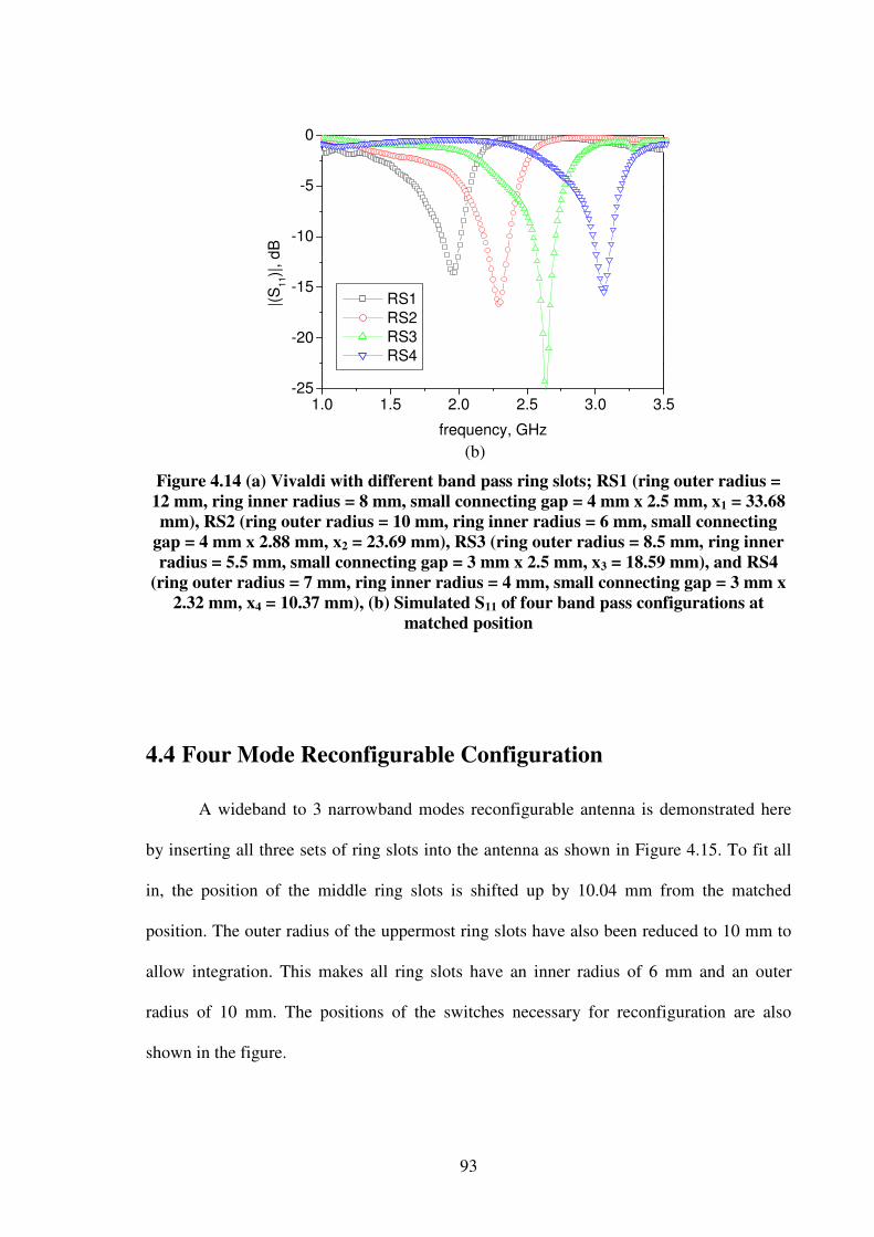
93
1.0 1.5 2.0 2.5 3.0 3.5-25
-20
-15
-10
-5
0
|(S
11)|
, d
B
frequency, GHz
RS1
RS2
RS3
RS4
(b)
Figure 4.14 (a) Vivaldi with different band pass ring slots; RS1 (ring outer radius =
12 mm, ring inner radius = 8 mm, small connecting gap = 4 mm x 2.5 mm, x1 = 33.68
mm), RS2 (ring outer radius = 10 mm, ring inner radius = 6 mm, small connecting
gap = 4 mm x 2.88 mm, x2 = 23.69 mm), RS3 (ring outer radius = 8.5 mm, ring inner
radius = 5.5 mm, small connecting gap = 3 mm x 2.5 mm, x3 = 18.59 mm), and RS4
(ring outer radius = 7 mm, ring inner radius = 4 mm, small connecting gap = 3 mm x
2.32 mm, x4 = 10.37 mm), (b) Simulated S11 of four band pass configurations at
matched position
4.4 Four Mode Reconfigurable Configuration
A wideband to 3 narrowband modes reconfigurable antenna is demonstrated here
by inserting all three sets of ring slots into the antenna as shown in Figure 4.15. To fit all
in, the position of the middle ring slots is shifted up by 10.04 mm from the matched
position. The outer radius of the uppermost ring slots have also been reduced to 10 mm to
allow integration. This makes all ring slots have an inner radius of 6 mm and an outer
radius of 10 mm. The positions of the switches necessary for reconfiguration are also
shown in the figure.
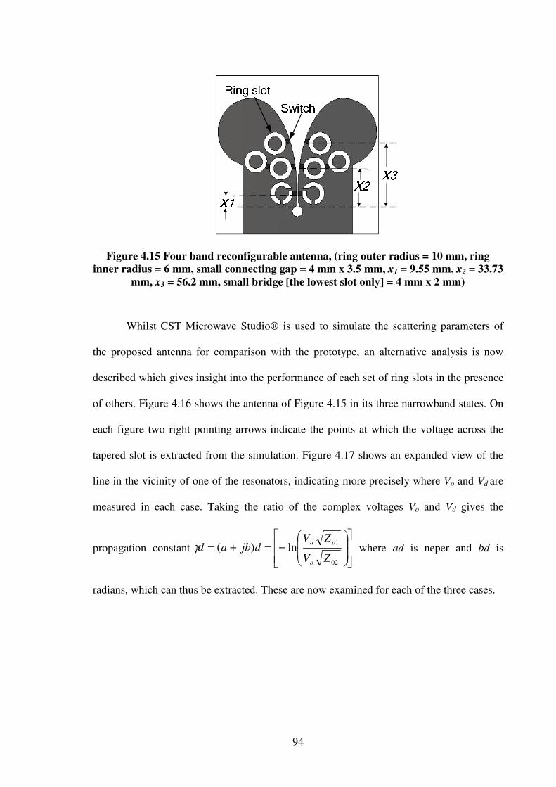
94
Figure 4.15 Four band reconfigurable antenna, (ring outer radius = 10 mm, ring
inner radius = 6 mm, small connecting gap = 4 mm x 3.5 mm, x1 = 9.55 mm, x2 = 33.73
mm, x3 = 56.2 mm, small bridge [the lowest slot only] = 4 mm x 2 mm)
Whilst CST Microwave Studio® is used to simulate the scattering parameters of
the proposed antenna for comparison with the prototype, an alternative analysis is now
described which gives insight into the performance of each set of ring slots in the presence
of others. Figure 4.16 shows the antenna of Figure 4.15 in its three narrowband states. On
each figure two right pointing arrows indicate the points at which the voltage across the
tapered slot is extracted from the simulation. Figure 4.17 shows an expanded view of the
line in the vicinity of one of the resonators, indicating more precisely where Vo and Vd are
measured in each case. Taking the ratio of the complex voltages Vo and Vd gives the
propagation constant
−=+=
02
1ln)(
ZV
ZVdjbad
o
odγ where ad is neper and bd is
radians, which can thus be extracted. These are now examined for each of the three cases.

95
(a) (b) (c)
Figure 4.16 (a) Low band- (b) Mid band- (c) High band configuration
Figure 4.17 Tapered slot line voltages
4.4.1 Narrow low band mode
The low band mode characteristic is shown in Figure 4.18. It can be seen that a
very high attenuation occurs from 1.25 to 3.2 GHz, and thus the structure prevents any
signals beyond 1.25 GHz propagating up the tapered slot. The minimum attenuation occurs
at 1.15 GHz. The positive value of ad, neper (ad > 0) means loss and/or standing waves

96
and a minima in ad or ad = 0, means a pass band or low loss travelling wave. Small
negative values of ad are due to small inaccuracies in the Zo1/Zo2 calculation, due to the slot
line impedance expressions having width limits below the slot width in the antenna. The
maximum attenuation in the rejection band depends on how lossy is the structure. Higher
loss in the structure reduces the attenuation in the stop band [78]. One way to increase the
rejection is by using a very low loss material such as superconductor.
0.8 1.0 1.2 1.4 1.6 1.8 2.0 2.2 2.4 2.6 2.8 3.0 3.2-1.5
-1.0
-0.5
0.0
0.5
1.0
1.5
2.0
2.5
frequency, GHz
ad
, n
ep
er
-180
-120
-60
0
60
120
180
ad
bd
bd, d
egre
e
Figure 4.18 Low band dispersions curve, (attenuation and phase)
4.4.2 Narrow mid band mode
Figure 4.19 shows the characteristic of the mid band mode structure. Its shows that
minimum attenuation occurs from 2.05 to 2.22. A high value of ad in the pass band region
reflects the low gain noticed in the Table 4.1. There is evidence of a pass band above
3.2 GHz, which is also noticed in the S11 plots shown in Figure 4.31b.
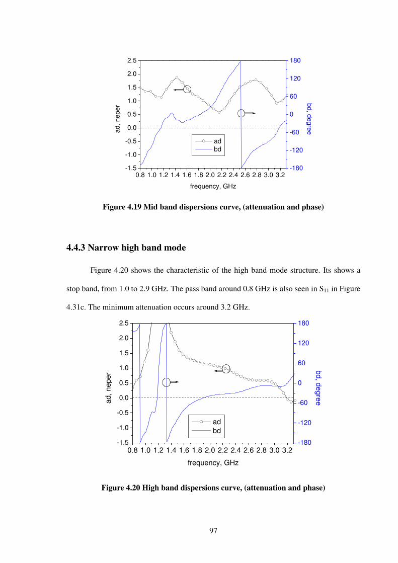
97
0.8 1.0 1.2 1.4 1.6 1.8 2.0 2.2 2.4 2.6 2.8 3.0 3.2-1.5
-1.0
-0.5
0.0
0.5
1.0
1.5
2.0
2.5
ad
bd
frequency, GHz
ad
, ne
pe
r
-180
-120
-60
0
60
120
180
bd
, de
gre
e
Figure 4.19 Mid band dispersions curve, (attenuation and phase)
4.4.3 Narrow high band mode
Figure 4.20 shows the characteristic of the high band mode structure. Its shows a
stop band, from 1.0 to 2.9 GHz. The pass band around 0.8 GHz is also seen in S11 in Figure
4.31c. The minimum attenuation occurs around 3.2 GHz.
0.8 1.0 1.2 1.4 1.6 1.8 2.0 2.2 2.4 2.6 2.8 3.0 3.2-1.5
-1.0
-0.5
0.0
0.5
1.0
1.5
2.0
2.5
ad
bd
frequency, GHz
ad
, n
ep
er
-180
-120
-60
0
60
120
180
bd
, de
gre
e
Figure 4.20 High band dispersions curve, (attenuation and phase)

98
The effects of the ring slots on the gain of the antenna can be analyzed by
comparing three antenna configurations, one without the ring slots (WR), as indicated in
Figure 4.1, one with the ring slots using ideal switches (ID), as shown in Figure 4.15, and
one with the ring slots using PIN diode switches (PD), as shown in Figure 4.27. Even
though the ring slots occupy a substantial part of the antenna surface, it is observed that the
difference in the gain between WR and ID antennas is small except from 2.6 to 3.2 GHz as
shown in Figure 4.21. On the other hand, Figure 4.22 compares the measured gain of the
ID and PD antennas in wideband mode. It is observed that the PIN diode switches have
effects on the gain degradation.
1.0 1.2 1.4 1.6 1.8 2.0 2.2 2.4 2.6 2.8 3.0 3.2-1
0
1
2
3
4
5
6
7
8
9
ga
in,
dB
i
frequency, GHz
ID
WR
Figure 4.21 Gain comparison between WR and ID antennas

99
1.0 1.2 1.4 1.6 1.8 2.0 2.2 2.4 2.6 2.8 3.0 3.2-1
0
1
2
3
4
5
6
7
8
ga
in,
dB
i
frequency, GHz
PIN
ID
Figure 4.22 Gain comparison between PIN and ID antennas
Further insight may be gained by examining the current distributions in the various
modes. The comparison between the simulated surface current distributions in the three
narrowband operative states and the wideband mode are shown in Figure 4.23. In general a
similar current distribution is observed between the low band and wideband configurations
when excited at the same frequency. The same behaviour is also observed between the
mid- and high band configuration. The current distributions excited beyond the operating
frequencies for low band configurations are also shown in Figure 4.24. It is clearly
observed that the current at the resonant frequency, 1.1 GHz, propagates through the upper
part of the antenna, as shown in Figure 4.23b. However most of the current at 2 and 3 GHz
is cut off by the lower ring slots, therefore stopping high frequency band operation. Figure
4.25 shows the current distributions for the mid band configuration excited at 1.1GHz and
3 GHz, and Figure 4.26 shows the current distributions for the high band configuration

100
excited at 1.1GHz and 2 GHz. It can clearly be seen that there is less current in the stop
band.
(a) (b)
(c) (d)
(e) (f)
Figure 4.23 Simulated surface current distributions for (a) Wideband configuration
excited at 1.1GHz, (b) Low band configuration excited at 1.1GHz, (c) Wideband
configuration excited at 2.2GHz, (d) Mid band configuration excited at 2.2GHz, (e)
Wideband configuration excited at 3.1GHz, (d) High band configuration excited at
3.1GHz

101
(a) (b)
Figure 4.24 Simulated current distributions for the low band configuration excited at
(a) 2 GHz and (b) 3 GHz
(a) (b)
Figure 4.25 Simulated current distributions for the mid band configuration excited at
(a) 1.1 GHz and (b) 3 GHz
(a) (b)
Figure 4.26 Simulated current distributions for the high band configuration excited at
(a) 1.1 GHz and (b) 2 GHz

102
4.5 Prototype Antenna
In the CST simulation, the PIN diode was modeled in its on state as a 2 Ω
resistance and in its off state using an S-parameter file supplied by the diode manufacturer.
The dc lines and dc decoupling components are included in the simulation. The practical
antenna is shown in Figure 4.27. To give a minimal effect on the radiation pattern, four
very thin dc lines were printed parallel to the beam direction on either side of the antenna.
Therefore if there are any RF leakages through the dc line, the effect will be negligible.
The dc line was isolated from the RF signal by using 27 nH SMD inductors. The tapered
slot is dc isolated into four sections with 0.3 mm width slots. To preserve RF continuity, 22
pF SMD capacitors bridged the slots every 10 mm. Each switch in Figure 4.15 consists of
two in-series Infineon PIN diodes, BAR50-02V. Two diodes are used in series because a
single diode having 1.2 mm length is unable to bridge the 4 mm gaps. Gaps of 4 mm are
used to reduce spurious resonances at higher frequency due to parasitic capacitance across
the gap sides. Figure 4.28 shows the simulated S11 with different sized gaps used for low
band operation. There is very small spurious when 4 mm gaps are used. Nevertheless,
further work might reveal alternative ways to design the gap that could be bridged by a
single diode having 1.2 mm length while avoiding spurious resonance problems. The
diodes were forward biased appropriately with dc voltage to obtain 100 mA on state bias
current. To obtain the off state, the diodes were left unbiased.

103
Figure 4.27 Prototype
(a)

104
0.5 1.0 1.5 2.0 2.5 3.0 3.5-20
-15
-10
-5
0
|S11|, d
B
frequency, GHz
Gap=1mm
Gap=1mm and tapered
Gap=1mm x 1mm
Gap=4mm
(b)
Figure 4.28 Spurious in S11 responses as a function of gap sizes.
4.6 Results
Figure 4.29 compares the simulated return loss for wideband operation with and
without the ring slots. It is noticed that the S11 between 1.8 and 3.0 GHz has been improved
by the ring slots. The simulated and the measured wideband responses with ring slots are
shown in Figure 4.30. Good agreement can be seen between them. The results show that a
good matching for wideband operation is achieved over a 1.0 – 3.2 GHz bandwidth. The
return loss for the other three states, low band 1.1 GHz, mid band 2.25 GHz and high band
3.1 GHz are shown in Figure 4.31. A small frequency shift between the measurement and
simulation is presumably due to the effect of parasitics in the PIN diodes, fabrication
tolerances and biasing components. However, in general, a good agreement has been
achieved.

105
0.8 1.0 1.2 1.4 1.6 1.8 2.0 2.2 2.4 2.6 2.8 3.0 3.2-40
-35
-30
-25
-20
-15
-10
-5
0
|S1
1|, d
B
frequency, GHz
simulated without ring slot
simulated with ring slot
Figure 4.29 Simulated wideband mode S11 response of antenna with and without ring
slots
0.8 1.0 1.2 1.4 1.6 1.8 2.0 2.2 2.4 2.6 2.8 3.0 3.2-40
-35
-30
-25
-20
-15
-10
-5
0
|S1
1|, d
B
frequency, GHz
measured
simulated
Figure 4.30 Simulated and measured wideband mode S11

106
0.8 1.0 1.2 1.4 1.6 1.8 2.0 2.2 2.4 2.6 2.8 3.0 3.2-30
-25
-20
-15
-10
-5
0
|S1
1|, d
B
frequency, GHz
measured
simulated
(a)
0.8 1.0 1.2 1.4 1.6 1.8 2.0 2.2 2.4 2.6 2.8 3.0 3.2-30
-25
-20
-15
-10
-5
0
|S1
1|, d
B
frequency, GHz
measured
simulated
(b)

107
0.8 1.0 1.2 1.4 1.6 1.8 2.0 2.2 2.4 2.6 2.8 3.0 3.2 3.4-30
-25
-20
-15
-10
-5
0
|S1
1|, d
B
frequency, GHz
measured
simulated
(c)
Figure 4.31 Simulated and measured S11 of antenna in narrowband modes (a) Low
band state (b) Mid band state (c) High band state.
The out of band rejection is relatively poor. This can only be expected as the
filtering or reconfiguration is achieved with single resonator which has relatively low Q
due to being mounted in an antenna, as well as the switch losses. However the main factor
of that relatively poor rejection in S11 mainly comes from the dielectric losses of the FR4
substrate. Figure 4.32 shows this, where the simulated S11 of lossy FR4 substrate of low
band mode is compared with the lossless case. The effect of the ideal and real switches on
the S11 is also compared as shown in Figure 4.33. It is seen that the loss that contributed to
poor rejection is small from the switch but very pronounced from the FR4 substrate.

108
0.8 1.0 1.2 1.4 1.6 1.8 2.0 2.2 2.4 2.6 2.8 3.0 3.2-20
-15
-10
-5
0
|S1
1|, d
B
frequency, GHz
sim lossless Ideal SW
sim lossy Ideal SW
Figure 4.32 Rejection in S11 as a function of substrate loss
0.8 1.0 1.2 1.4 1.6 1.8 2.0 2.2 2.4 2.6 2.8 3.0 3.2-25
-20
-15
-10
-5
0
|S1
1|, d
B
frequency, GHz
sim Ideal SW
sim lossy Real SW
Figure 4.33 Rejection in S11 as a function of switch loss
To give a better measure of out of band rejection, the measured return loss and gain
vs frequency for each narrow band mode and the wideband mode is presented. The low
band mode achieved a comparable gain with the wideband mode at the pass band region
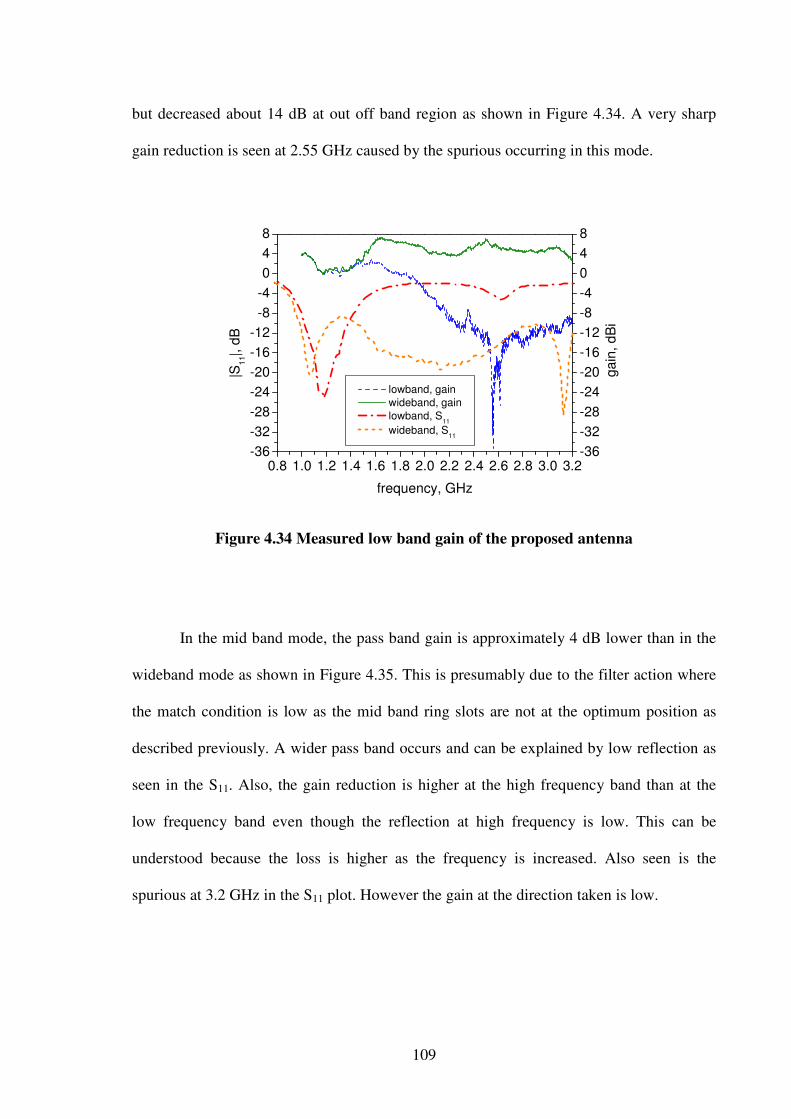
109
but decreased about 14 dB at out off band region as shown in Figure 4.34. A very sharp
gain reduction is seen at 2.55 GHz caused by the spurious occurring in this mode.
0.8 1.0 1.2 1.4 1.6 1.8 2.0 2.2 2.4 2.6 2.8 3.0 3.2-36
-32
-28
-24
-20
-16
-12
-8
-4
0
4
8
-36
-32
-28
-24
-20
-16
-12
-8
-4
0
4
8
ga
in,
dB
i
|S1
1|, d
B
frequency, GHz
lowband, gain
wideband, gain
lowband, S11
wideband, S11
Figure 4.34 Measured low band gain of the proposed antenna
In the mid band mode, the pass band gain is approximately 4 dB lower than in the
wideband mode as shown in Figure 4.35. This is presumably due to the filter action where
the match condition is low as the mid band ring slots are not at the optimum position as
described previously. A wider pass band occurs and can be explained by low reflection as
seen in the S11. Also, the gain reduction is higher at the high frequency band than at the
low frequency band even though the reflection at high frequency is low. This can be
understood because the loss is higher as the frequency is increased. Also seen is the
spurious at 3.2 GHz in the S11 plot. However the gain at the direction taken is low.

110
0.8 1.0 1.2 1.4 1.6 1.8 2.0 2.2 2.4 2.6 2.8 3.0 3.2-36
-32
-28
-24
-20
-16
-12
-8
-4
0
4
8
-36
-32
-28
-24
-20
-16
-12
-8
-4
0
4
8
ga
in,
dB
i
|S1
1|, d
Bi
frequency, GHz
midband, gain
wideband, gain
midband, S11
wideband, S11
Figure 4.35 Measured mid band gain of the proposed antenna
The pass band gain in the high band mode shown in Figure 4.36 is nearly
comparable with the wideband gain as the matching is good. The gain is gradually dropped
as the reflection is slowly increased in the rejection band. Also the gain is seen to increase
below 1.0 GHz where the pass band occurs at 0.9 GHz. Table 4.1 compares the measured
and simulated gains for each state. In the narrowband state, the roll off at the edge of the
pass bands is not fast. This is presumably related to the fact that the antenna itself is
inherently wideband and also as expected since the antenna is a low Q radiator.
0.8 1.0 1.2 1.4 1.6 1.8 2.0 2.2 2.4 2.6 2.8 3.0 3.2 3.4-36
-32
-28
-24
-20
-16
-12
-8
-4
0
4
8
-36
-32
-28
-24
-20
-16
-12
-8
-4
0
4
8
ga
in,
dB
i
|S11|, d
B
frequency, GHz
highband, gain
wideband, gain
highband, S11
wideband, S11
Figure 4.36 Measured high band gain of the proposed antenna

111
The E- and H-plane simulated and measured radiation patterns are presented in
Figure 4.37. Good agreement between simulation and measurement has been achieved. It
can be concluded that the biasing circuit has a small effect on the antenna performance. It
is also observed that the 3 dB beam width becomes narrower as the frequency increases,
which is usual for the Vivaldi antenna. The cross-polar radiation pattern in particular the
main direction is lower than -10 dB. It is suggested that the ring slot resonators have some
effect on cross polar radiation performance.
-30
-20
-10
0
60
120
30
150
0
180
30
150
60
120
90 90
-30
-20
-10
0
60
120
30
150
0
180
30
150
60
120
90 90
(a)
-30
-20
-10
0
60
120
30
150
0
180
30
150
60
120
90 90
-30
-20
-10
0
60
120
30
150
0
180
30
150
60
120
90 90
(b)

112
-30
-20
-10
0
60
120
30
150
0
180
30
150
60
120
90 90
-30
-20
-10
0
60
120
30
150
0
180
30
150
60
120
90 90
(c)
-30
-20
-10
0
60
120
30
150
0
180
30
150
60
120
90 90
-30
-20
-10
0
60
120
30
150
0
180
30
150
60
120
90 90
(d)
co-polar simulated ----- co-polar measured
-o-o- cross-polar simulated -x-x- cross-polar measured
Figure 4.37 Radiation pattern. (a) Low band mode excited at 1.1 GHz, E-plane (left),
H-plane (right). (b) Mid band mode exited at 2.2 GHz, E-plane (left) , H-plane (right).
(c) High band mode excited at 3.1 GHz E-plane (left) , H-plane (right). (d) Wideband
mode excited at 2.0 GHz, E-plane (left) , H-plane (right).
Table 4.1 Gain of the proposed antenna
Gain, dBi Wide band
(at 2 GHz) High band Mid band Low band
Simulated 3.61 3.31 0.57 1.75
Measured 3.27 1.56 0.28 1.47

113
4.7 Summary
A novel switched band Vivaldi antenna has been proposed by introducing the ring
slots. Three modes of reconfiguration are shown, when three pairs of ring slots were
employed in three different positions within the Vivaldi. The design guideline has been
derived and allows some optimizing of the band positions. More sub-bands could be
achieved with additional resonators, in a longer version of the antenna. Nevertheless, in the
relatively simple example shown, good return loss has been obtained for each of the sub
bands. The proposed antenna could be a suitable solution for applications requiring
wideband sensing and dynamic band switching, such as in military application or cognitive
radio. The work described here has been published in [83-86].

114
CHAPTER 5
VIVALDI WITH SINGLE RING RESONATOR
5.1 Introduction
In the previous chapter, a Vivaldi antenna incorporating multiple rings has been
demonstrated. The antenna shows band switching between a wideband mode (1.0 - 3.2
GHz) and three narrowband modes. In that configuration, the number of frequency bands
controlled depends on the number of resonators incorporated. This means that if more
bands were desired, the antenna has to be much longer to incorporate more resonators. In
this chapter a new design method of band switching in the Vivaldi antenna, that allows a
better control of the narrow operating bands, is proposed. By incorporating only a single
pair of slot resonators, six different narrow frequency bands can be switched within the
wideband operation, double the number reported in the previous chapter. To achieve the
switched band properties, the proposed approach reconfigures the operating band by
varying the electrical length of the slot resonators by means of PIN diode switches. This
effectively stops, or passes, current at different frequencies. The design principles of the

115
proposed antenna are described. Section 5.2 and 5.3 discuss the initial design of the
Vivaldi antenna and the switchable slot line resonator. In section 5.4, the switchable
narrowband antenna configuration is explained. The fabricated antenna is discussed in
section 5.5. Finally the results are presented in section 5.6 and followed by conclusions in
section 5.7.
5.2 Wideband Antenna Design
The reconfigurable antenna is based on the same wideband Vivaldi antenna
operating from 1 to 3 GHz as described in previous chapter. The Vivaldi is illustrated in
Figure 5.1. The simulated S11, in Figure 5.2, shows that 1 – 3 GHz wideband operation is
achieved.
(a)
(b)
Figure 5.1 Vivaldi antenna, (a) front view, (b) rear view showing microstrip feed.

116
0.8 1.2 1.6 2.0 2.4 2.8 3.2-40
-30
-20
-10
0
|S11|, d
B
frequency, GHz
Figure 5.2 S11 of Vivaldi antenna in Figure 5.1
5.3 Slot Line Resonator Design
In principle, distorting the current distributions along the antennas current path will
change the radiation properties. The Vivaldi has currents that propagate near the edge of
the tapered slot, as shown in Figure 5.3. The narrower end is acting as a transmission
region whilst the wider end is acting as a radiation region. It is thus appropriate to locate
the filter in the narrower end. A slot ring resonator with a perimeter, Ps as shown in Figure
5.4 is chosen for this. The basic principle of the reconfigurable ring slot band pass
resonator is described below.
Figure 5.3 Simulated surface current distribution at 2 GHz

117
Figure 5.4 Slot ring resonator
A pass band response can be obtained either by cascading two different quarter
wavelength short circuit stubs in series to form two different stop band filters or by having
a single half wavelength short circuit stub. A possible equivalent circuit of two different
stop band filters in series is shown in Figure 5.5. Two parallel RLC circuits are arranged in
series, where each parallel RLC circuit represents a stop band filter. Figure 5.6 shows the
response simulated using Microwave Office AWR software when L1, C1, R1 and L2, C2, R2
are set to (45 nH, 0.41 pF, 82.9 kΩ) and (24.61 nH, 0.154 pF, 21.15 kΩ) respectively. It is
clearly seen that two stop bands occur at 1.17 GHz and 2.59 GHz which correspond to the
resonances of circuit one and two respectively. Together, the circuits form a band pass
filter at 1.68 GHz. Therefore, the slot ring resonator is designed in such a way to form two
stop band filters in series. The slot ring design is now described.

118
CAPID=C1
PORTP=2
PORTP=1
RESID=R2
RESID=R1
INDID=L2
INDID=L1
CAPID=C2
Figure 5.5 RLC shunt circuits in series
1 1.2 1.4 1.6 1.8 2 2.2 2.4 2.6 2.8 3
frequency, GHz
-60
-50
-40
-30
-20
-10
0
s-p
ara
me
ters
, d
B
2.59 GHz-46.55 dB
1.68 GHz-19.49 dB
1.17 GHz-56.33 dB
|(S1,1)|
|(S2,1)|
Figure 5.6 Simulated s-parameters of RLC shunt circuits in series
The shape of the ring slots is chosen so that two tunable stop band filter in series can be
easily designed. They have an inner radius of 8 mm and an outer radius of 12 mm. Small
gaps, of size 3.67 mm x 4 mm are used to couple the resonator to the slot line. Figure 5.7a
shows a single stop band filter configuration, stopping at 1.69 GHz. The ring slot is acting

119
as an open circuit stub, where its average perimeter Ps = 72 mm is approximately a half
wavelength at 1.69 GHz. Since the slot length determines the stop band frequency, it is
now possible to form two stop band filters by bridging the slot at an appropriate location.
Figure 5.8 shows the configuration required to obtain a band pass response at 1.68 GHz.
Instead of acting as a single open circuit stub, the slot now has two short circuit stubs in
series which have different length P1 and P2, giving two stop band responses. P1 = 18 mm
represents a quarter wavelength at 3.2 GHz while P2 = 54 mm represents a quarter
wavelength at 1.13 GHz.
(a)
1.0 1.2 1.4 1.6 1.8 2.0 2.2 2.4 2.6 2.8 3.0-40
-30
-20
-10
0
s-p
ara
me
ters
, dB
frequency, GHz
S11
S21
(b)
Figure 5.7 Single stop band filter, (a) the configuration, (b) the responses

120
(a)
1.0 1.2 1.4 1.6 1.8 2.0 2.2 2.4 2.6 2.8 3.0-40
-30
-20
-10
0
s-p
ara
me
ters
, d
B
frequency, GHz
S11
S21
(b)
Figure 5.8 Band pass filter, (a) the configuration, (b) the responses
To switch to a different pass band, the bridges are moved to other specific positions,
changing the electrical length of P1 and P2. Alternatively an extra bridge can be added. For
example, Figure 5.9 shows how a new band pass configuration at 2.3 GHz is achieved after
an extra bridge is added in the ring slot. P2 is reduced to 36 mm representing a quarter
wavelength at 1.68 GHz, whilst P1 is kept to 18 mm.

121
(a)
1.0 1.2 1.4 1.6 1.8 2.0 2.2 2.4 2.6 2.8 3.0-40
-30
-20
-10
0
s-p
ara
me
ters
, dB
frequency, GHz
S11
S21
(b)
Figure 5.9 Band pass filter, (a) the configuration, (b) the responses
Alternatively, the pass band response can also be obtained by transforming the slot
ring in Figure 5.4 to a half wavelength short circuit stub by bridging the slot at the position
shown in Figure 5.10. The total length, P from the edge of the small gaps is approximately
a half wavelength (78 mm) at 1.52 GHz. To switch the frequency, an extra bridge is added
to shorten the length. The different pass band configurations as a function of bridge
position are summarized in Figure 5.11.

122
Figure 5.10 Pass band configuration using a half wavelength short circuited stub
Switch location and Pass band
Band1 1.52 GHz
Band4 2.01 GHz
Band2 1.65 GHz
Band5 2.34 GHz
Band3 1.76 GHz
Band6 2.88 GHz
Asymmetric position: Band 1, Band 2, Band 3, Band 4 and Band 6
Symmetric position: Band 5
Figure 5.11 Bridge position for various pass band centre frequencies
The use of different forms of pass band circuit is useful to reduce number of
switches. For example, the same switch used in Band 1 and Band 2 is also being used in
Band 3. Band 2 is using two stop bands in series to operate at 1.65 GHz, whilst Band 1 and
Band 3 is operated using a half wavelength short circuit stub method. As also can be seen
in Figure 5.11, most of the relative switch positions are asymmetric rather than symmetric.
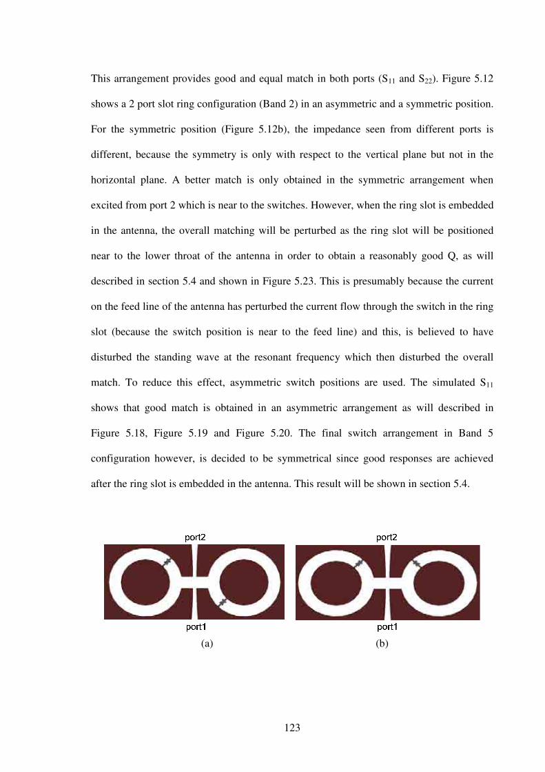
123
This arrangement provides good and equal match in both ports (S11 and S22). Figure 5.12
shows a 2 port slot ring configuration (Band 2) in an asymmetric and a symmetric position.
For the symmetric position (Figure 5.12b), the impedance seen from different ports is
different, because the symmetry is only with respect to the vertical plane but not in the
horizontal plane. A better match is only obtained in the symmetric arrangement when
excited from port 2 which is near to the switches. However, when the ring slot is embedded
in the antenna, the overall matching will be perturbed as the ring slot will be positioned
near to the lower throat of the antenna in order to obtain a reasonably good Q, as will
described in section 5.4 and shown in Figure 5.23. This is presumably because the current
on the feed line of the antenna has perturbed the current flow through the switch in the ring
slot (because the switch position is near to the feed line) and this, is believed to have
disturbed the standing wave at the resonant frequency which then disturbed the overall
match. To reduce this effect, asymmetric switch positions are used. The simulated S11
shows that good match is obtained in an asymmetric arrangement as will described in
Figure 5.18, Figure 5.19 and Figure 5.20. The final switch arrangement in Band 5
configuration however, is decided to be symmetrical since good responses are achieved
after the ring slot is embedded in the antenna. This result will be shown in section 5.4.
(a) (b)

124
1.0 1.2 1.4 1.6 1.8 2.0 2.2 2.4 2.6 2.8 3.0 3.2-30
-25
-20
-15
-10
-5
0
|S1
1|, d
B
frequency, GHz
symmetric port1
symmetric port2
asymmetric
(c)
Figure 5.12 2 port (a) Asymmetric, and (b) Symmetric position on (c) S11 responses
The effect of ring radius on the pass band frequency is studied. Figure 5.13 shows
this. As resonant frequency is inversely proportional to the length of the ring slot in guided
wavelengths, reducing the outer radius, ro, from 12 mm to 8 mm and inner radius ri, from 8
mm to 4 mm respectively, shifts the pass band response from 1.68 GHz to 2.72 GHz. If a
smaller ring slot as in the configuration shown in Figure 5.13a is chosen, narrowband
operation lower than 2 GHz, will be impossible to obtain.
(a)

125
1.0 1.2 1.4 1.6 1.8 2.0 2.2 2.4 2.6 2.8 3.0-40
-30
-20
-10
0
ro = 8 mm
ri = 4 mm
ro = 12 mm
ri = 8 mm
|S1
1|, d
B
frequency, GHz
(b)
Figure 5.13 Effect of slot ring radius (a) configuration, (b) responses for outer radius,
r = 12mm and 8 mm, with inner radius = 8mm and 4 mm respectively
The width of the slot ring is important to determine the quality factor, Q. Figure
5.14 shows the Q at the pass band is decreased when the slot gap, G, reduced from 4 to 1
mm. Therefore the Q of a 4 mm was chosen to demonstrate the action and final choice may
depend on application.
(a)

126
1.0 1.2 1.4 1.6 1.8 2.0 2.2 2.4 2.6 2.8 3.0-40
-30
-20
-10
0
|S2
1|
frequency, GHz
Gap..1mm
Gap..4mm
(b)
Figure 5.14 Effect of slot ring width (a) configuration, inner radius, = 8 mm, (b)
responses for gap, G = 4 mm and 1 mm, with outer radius = 12 mm and 9 mm
respectively
.
5.4 Seven Mode Reconfigurable Configuration
The design and simulation of a Vivaldi antenna with seven modes is now described.
To reconfigure the antenna electronically, the CST simulation uses on state s2p-data of
Infineon PIN diode switches, model BAR50-02V to represent the on state. To simplify the
simulation process, the off state is represented by a gap. Also to reduce computation time,
there are neither dc lines nor dc decoupling components included in the simulation. An
example of Band 2 (Figure 5.11) configuration is shown in Figure 5.15. The ring slot is
placed x = 21.26 mm above the circular slot stub to reduce strong coupling from the feed
line located on the reverse side of the substrate. When using ideal switches, consisting of
metal pads of size 1 mm x 4 mm, the simulated resonance of Band 2 configuration occurs
at 1.7 GHz. However with Infineon PIN diode switch models, the simulated resonance is

127
shifted down around 14.7% to 1.45 GHz. This can be explained by the package parasitic
effects. The simulated S11 results are shown in Figure 5.16.
Figure 5.15 Band 2 configuration, x = 21.26 mm
1.0 1.2 1.4 1.6 1.8 2.0 2.2 2.4 2.6 2.8 3.0-25
-20
-15
-10
-5
0
|S1
1|, d
B
frequency, GHz
ideal
PIN diode
Figure 5.16 Simulated S11 of band 2 configuration
Figure 5.17 shows the current distributions of Band 2 configuration using ideal
switches when excited at the resonance frequency, 1.7 GHz (Figure 5.17a) and at out of

128
band frequencies 1 GHz (Figure 5.17b) and 3 GHz (Figure 5.17c). It is observed that the
ring slot, passes the current at 1.7 GHz but significantly reduces the current on the upper
part of the antenna at 1 and 3 GHz.
(a)
(b) (c)
Figure 5.17 Current distributions (a) excited at 1.7 GHz, (b) excited at 1.0 GHz, (c)
excited at 3.0 GHz.
The effects of the switch arrangement style (asymmetric or symmetric) for Band 2
are shown in Figure 5.18 and Figure 5.19. It is observed symmetric arrangements gave
poor impedance match and good match is only obtained when asymmetric arrangement is
used. Figure 5.20 shows the effect of asymmetric and symmetric arrangements for the

129
other bands. Generally, an asymmetric arrangement give a good match hence a good return
loss in all bands, however at some frequencies i.e. in Band 5 and Band 6, it is observed that
a symmetric arrangement also give a good match.
(a)
1.0 1.2 1.4 1.6 1.8 2.0 2.2 2.4 2.6 2.8 3.0-25
-20
-15
-10
-5
0
|S1
1|, d
B
frequency, GHz
symmetric A
asymmetric
(b)
Figure 5.18 Asymmetric vs symmetric type A, (a) symmetric type A arrangement and
(b) the S11
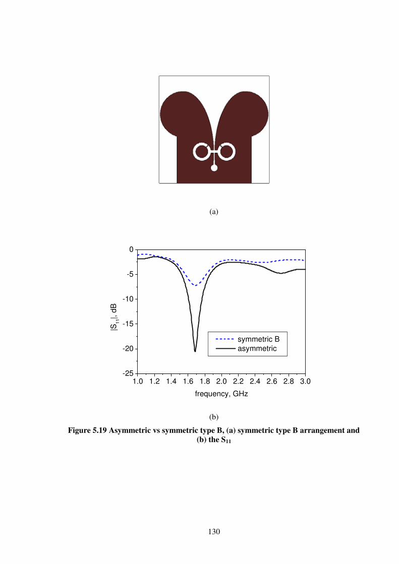
130
(a)
1.0 1.2 1.4 1.6 1.8 2.0 2.2 2.4 2.6 2.8 3.0-25
-20
-15
-10
-5
0
|S1
1|, d
B
frequency, GHz
symmetric B
asymmetric
(b)
Figure 5.19 Asymmetric vs symmetric type B, (a) symmetric type B arrangement and
(b) the S11

131
1.0 1.2 1.4 1.6 1.8 2.0 2.2 2.4 2.6 2.8 3.0-30
-25
-20
-15
-10
-5
0
Band1
|S1
1|, d
B
frequency, GHz
symmetric
asymmetric
(a)
1.0 1.2 1.4 1.6 1.8 2.0 2.2 2.4 2.6 2.8 3.0-30
-25
-20
-15
-10
-5
0
Band2
|S1
1|, d
B
frequency, GHz
symmetric
asymmetric
(b)

132
1.0 1.2 1.4 1.6 1.8 2.0 2.2 2.4 2.6 2.8 3.0-30
-25
-20
-15
-10
-5
0
Band3
|S1
1|, d
B
frequency, GHz
symmetric
asymmetric
(c)
1.0 1.2 1.4 1.6 1.8 2.0 2.2 2.4 2.6 2.8 3.0-30
-25
-20
-15
-10
-5
0
Band4
|S1
1|, d
B
frequency, GHz
symmetric
asymmetric
(d)

133
1.0 1.2 1.4 1.6 1.8 2.0 2.2 2.4 2.6 2.8 3.0-30
-25
-20
-15
-10
-5
0
Band5
|S1
1|, d
B
frequency, GHz
symmetric
asymmetric
(e)
1.0 1.2 1.4 1.6 1.8 2.0 2.2 2.4 2.6 2.8 3.0 3.2-30
-25
-20
-15
-10
-5
0
Band6
|S1
1|, d
B
frequency, GHz
symmetric
asymmetric
(f)
Figure 5.20 Effects of symmetric and asymmetric slot configuration on the matching

134
An asymmetric arrangement has an effect on the radiation pattern as shown in
Figure 5.21. The symmetry of the radiation pattern is slightly perturbed but on the whole
the radiation pattern is well behaved and the perturbation is hardly noticeable in the E-
plane and H-plane polar plot as shown in Figure 5.22. A symmetric radiation pattern is
good, but in that configuration a low match or high reflection will result. Further work
might reveal better return loss in a symmetric arrangement by positioning the ring slot
section at the right position. As described in chapter 4 and reported in [85], the right
position of the ring slot section may improve the frequency response.
(a) (b)
Figure 5.21 3-D pattern for Band 2 excited at 1.65 GHz, (a) asymmetric-, (b)
symmetric arrangement

135
-30
-20
-10
0
10
60
120
30
150
0
180
30
150
60
120
90 90
-30
-20
-10
0
10
60
120
30
150
0
180
30
150
60
120
90 90
–––––– asymmetric, – – – – – symmetric
(a) (b)
Figure 5.22 Polar plot for Band 2 excited at 1.65 GHz, (a) E-plane, (b) H-plane
The effect of the positions of the ring slot is examined by moving it up toward the
wider end (x = 36.26 mm) of the tapered slot as shown in Figure 5.23a. The pass band
become wider at the upper end band, as can be seen in Figure 5.23b. It is presumed that the
ring slot has little current interception at high frequencies, thus reducing the quality factor.
Similar behaviour is also noticed for Band 1, Band 3, and Band 4 after the ring slot is
positioned at x = 36.26 mm. Bands 5 and 6, however, show poor match. Figure 5.24 shows
this. Therefore the x1 position is chosen for a relatively high Q and good impedance
matching.

136
= 36.26 mm
(a)
1.0 1.2 1.4 1.6 1.8 2.0 2.2 2.4 2.6 2.8 3.0-30
-20
-10
0
|S11|, d
B
frequency, GHz
x = 21.26 mm
x = 36.26 mm
(b)
Figure 5.23 (a) Band 2 configurations, x = 36.26 mm (b) simulated S11 when ring slot
at x = 21.26 mm and x = 36.26 mm.

137
1.0 1.2 1.4 1.6 1.8 2.0 2.2 2.4 2.6 2.8 3.0-30
-20
-10
0
|S1
1|, d
B
frequency, GHz
x = 21.26 mm
x = 36.26 mm
(a)
1.0 1.2 1.4 1.6 1.8 2.0 2.2 2.4 2.6 2.8 3.0-30
-20
-10
0
|S11|, d
B
frequency, GHz
x = 21.26 mm
x = 36.26 mm
(b)

138
1.0 1.2 1.4 1.6 1.8 2.0 2.2 2.4 2.6 2.8 3.0-30
-25
-20
-15
-10
-5
0
|S1
1|, d
B
frequency, GHz
x = 21.26 mm
x = 36.26 mm
(c)
1.0 1.2 1.4 1.6 1.8 2.0 2.2 2.4 2.6 2.8 3.0-30
-20
-10
0
|S1
1|,d
B
frequency, GHz
x = 21.26 mm
x = 36.26 mm
(d)

139
1.0 1.2 1.4 1.6 1.8 2.0 2.2 2.4 2.6 2.8 3.0 3.2-30
-20
-10
0
|S1
1|, d
B
frequency, GHz
x = 21.26 mm
x = 36.26 mm
(e)
Figure 5.24 Simulated S11 (a) Band 1, (b) Band 3, (c) Band 4, (d) Band 5, (e) Band 6
when ring slot at x = 21.26 mm and x = 36.26 mm position.
The switch on state resistance has an effect on the impedance match and antenna
efficiency. Figure 5.25 shows the simulated S11 as a function of the on state resistance
between 0 and 8 Ω. The return loss degrades as the resistance is increased. Table 5.1
compares the simulated antenna efficiency and gain for different on state resistances. The
PIN diodes noted previously and MEMs switch model RMSW100 from Radant Mems,
including package parasitics, have also been compared in simulation. The simulated S11 of
Band 2 and Band 5 are shown in Figure 5.26. The MEMS switch has lower on state
resistances than PIN diode switches, thus giving the higher efficiency and gain as noted in
Table 5.2.

140
1.0 1.2 1.4 1.6 1.8 2.0 2.2 2.4 2.6 2.8 3.0-25
-20
-15
-10
-5
0
|S1
1|, d
B
frequency, GHz
0 Ω
4 Ω
8 Ω
Figure 5.25 Effects of On state resistance on S11
Table 5.1 Simulated Antenna Efficiency and Gain for Band 2 Configuration with
Different ON State Resistance Values
Rs 0 Ω 4 Ω 8 Ω
Efficiency, % 80.2 41.88 27.48
Gain, dBi 4.94 2.34 0.56
1.0 1.2 1.4 1.6 1.8 2.0 2.2 2.4 2.6 2.8 3.0-25
-20
-15
-10
-5
0
Band 5
Band 2
|(S
11)|
, d
B
frequency, GHz
Mems
PIN Diode
Figure 5.26 Effects of PIN diode and MEMs switches on S11 responses

141
Table 5.2 Simulated Efficiency and Gain for Band 2 and Band 5 Configuration for
Different Type of Switches
Switch
PIN diode
MEMs
Band 2 Band 5 Band 2 Band 5
Efficiency, % 51.92 47.92 69.51 61.1
Gain, dBi 3.23 1.69 4.43 2.71
5.5 Antenna Construction and Measurements
The configuration of the reconfigurable Vivaldi antenna including switch bias is
presented in Figure 5.27. Switches are placed at specific locations along the ring resonators
in order to achieve specific frequency bands as summarized in Figure 5.11.
Figure 5.27 The proposed antenna diagram

142
There are seven switches used on the left ring and eight switches used on the right.
Two switches in the small gaps at each side are used to decouple the resonator from the
tapered slot, whilst the rest of the switches are used to vary the effective electrical lengths
of the ring resonator by using different combinations of the on and off states. Infineon PIN
diodes switches, model BAR50-02V, are used. The diodes were forward biased
appropriately with dc voltage to obtain 100 mA on state bias current. To obtain the off
state, the diodes were left unbiased. In order to bias the switches appropriately, several
0.3 mm dc lines were printed parallel to the beam direction on either side of the antenna.
The dc line is isolated from the RF signal by using 27 nH SMD inductors. On the antenna
radiating part itself, 0.3 mm width slots are created for dc isolation. The RF continuity is
preserved by bridging the slots every 10 mm with 22 pF SMD capacitors. Two switches
each having 1.2 mm length, are needed to bridge the slot gaps of 4 mm on each side.
5.6 Results
Figure 5.28 compares the simulated return loss for wideband operation with and without
the ring slots. It is noticed that the S11 at 1.3 GHz and between 2.0 and 3.0 GHz has been
improved by the ring slots. The simulated and measured wideband responses of the
proposed antenna with ring slots are shown in Figure 5.29. To select the wideband mode,
the slot resonators are decoupled from the tapered slot edges. Wideband operation is
obtained over a 1 – 3 GHz bandwidth with a very good agreement between them. To select
the narrowband mode, the slot resonators are coupled through the gaps. By short circuiting
a specific set of diodes as indicated in Figure 5.11, the narrowband modes are achieved.
The measured return loss for the six narrow band states are shown in Figure 5.30. The
simulated and measured S11 for each of the narrow band states (1.45 GHz, 1.53 GHz, 1.66

143
GHz, 1.93 GHz, 2.11 GHz and 2.23 GHz) are compared in Figure 5.31. In general, a good
agreement has been achieved. Small frequency shifts can be accounted for by the
fabrication tolerance, the diode package parasitics and bias components. The rejection
band S11 levels are relatively poor. These are presumably due to switch losses as well as
the filter action. A better measure of the rejection would be a plot of gain vs frequency as
shown in Figure 5.32. Overall, good rejection is obtained in each narrow band mode as
seen in the gain plot. The gain is decreased around 4 – 6 dB (in Band 1 to Band 4) at
3.0 GHz even though the S11 levels shown are about -5 to -7 dB. The practical
measurement standard equipment setup for gain and radiation pattern is described in
Appendix B. The antenna is mounted using L bend SMA feed as shown in Figure B4.
0.8 1.0 1.2 1.4 1.6 1.8 2.0 2.2 2.4 2.6 2.8 3.0-20
-15
-10
-5
0
|S1
1|, d
B
frequency, GHz
without ring
with ring
Figure 5.28 Simulated wideband mode S11 response with and without ring slots

144
0.8 1.0 1.2 1.4 1.6 1.8 2.0 2.2 2.4 2.6 2.8 3.0-30
-25
-20
-15
-10
-5
0
|S1
1|, d
B
frequency, GHz
Meas
Sim
Figure 5.29 Wideband mode S11 response of the proposed antenna
1.0 1.2 1.4 1.6 1.8 2.0 2.2 2.4 2.6 2.8 3.0-30
-25
-20
-15
-10
-5
0
|S1
1|, d
B
frequency, GHz
Band1
Band2
Band3
Band4
Band5
Band6
Figure 5.30 Measured narrow band mode S11 of the proposed antenna

145
1.0 1.2 1.4 1.6 1.8 2.0 2.2 2.4 2.6 2.8 3.0-30
-25
-20
-15
-10
-5
0
|S1
1|, d
B
frequency, GHz
Meas
Sim
(a)
1.0 1.2 1.4 1.6 1.8 2.0 2.2 2.4 2.6 2.8 3.0-30
-25
-20
-15
-10
-5
0
|S1
1|,d
B
frequency, GHz
Meas
Sim
(b)

146
1.0 1.2 1.4 1.6 1.8 2.0 2.2 2.4 2.6 2.8 3.0-30
-25
-20
-15
-10
-5
0
|S1
1|, d
B
frequency, GHz
Meas
Sim
(c)
1.0 1.2 1.4 1.6 1.8 2.0 2.2 2.4 2.6 2.8 3.0-30
-25
-20
-15
-10
-5
0
|S1
1|, d
B
frequency, GHz
Meas
Sim
(d)
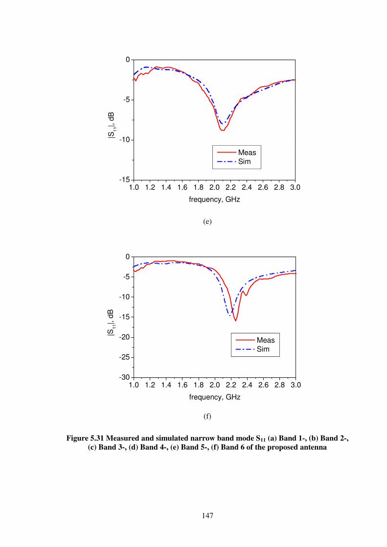
147
1.0 1.2 1.4 1.6 1.8 2.0 2.2 2.4 2.6 2.8 3.0-15
-10
-5
0
|S1
1|, d
B
frequency, GHz
Meas
Sim
(e)
1.0 1.2 1.4 1.6 1.8 2.0 2.2 2.4 2.6 2.8 3.0-30
-25
-20
-15
-10
-5
0
Meas
Sim
|S1
1|, d
B
frequency, GHz
(f)
Figure 5.31 Measured and simulated narrow band mode S11 (a) Band 1-, (b) Band 2-,
(c) Band 3-, (d) Band 4-, (e) Band 5-, (f) Band 6 of the proposed antenna
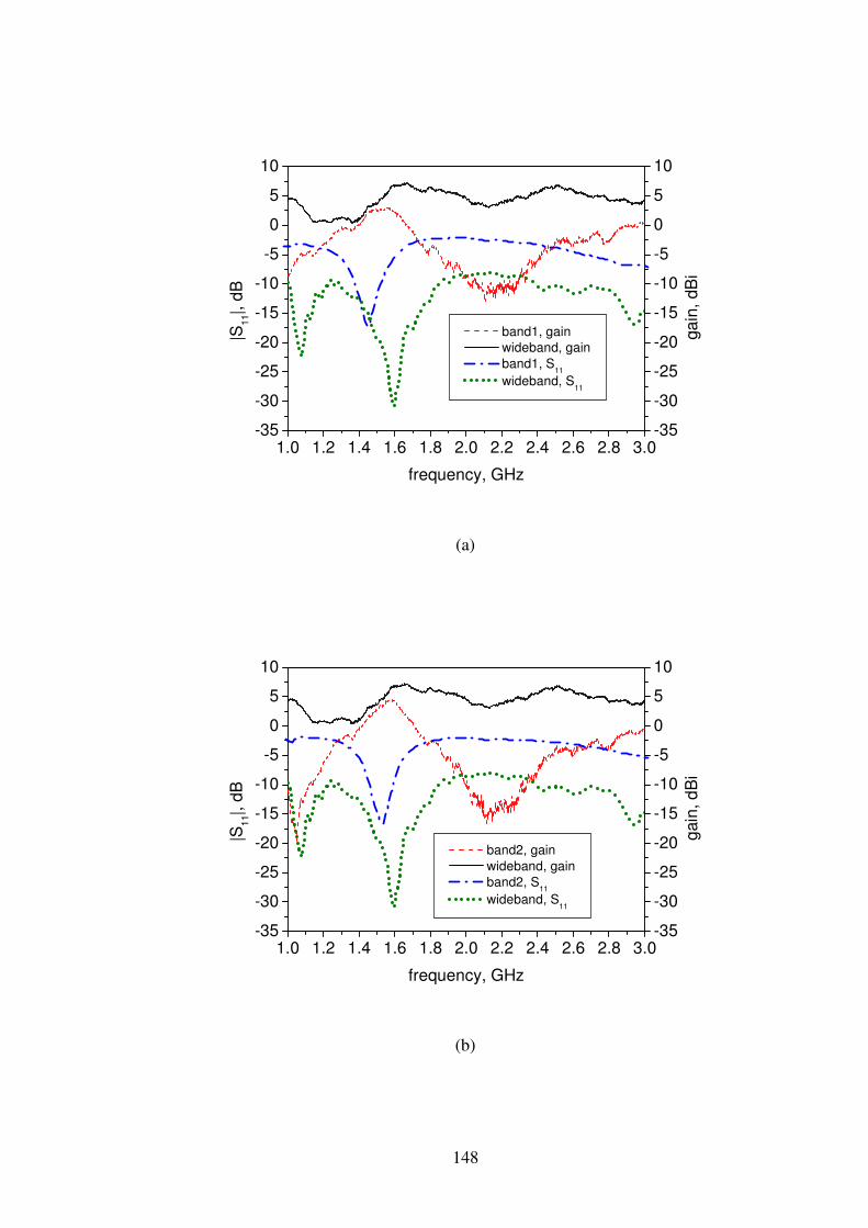
148
1.0 1.2 1.4 1.6 1.8 2.0 2.2 2.4 2.6 2.8 3.0-35
-30
-25
-20
-15
-10
-5
0
5
10
-35
-30
-25
-20
-15
-10
-5
0
5
10
ga
in,
dB
i
|S11|, d
B
frequency, GHz
band1, gain
wideband, gain
band1, S11
wideband, S11
(a)
1.0 1.2 1.4 1.6 1.8 2.0 2.2 2.4 2.6 2.8 3.0-35
-30
-25
-20
-15
-10
-5
0
5
10
-35
-30
-25
-20
-15
-10
-5
0
5
10
gain
, d
Bi
|S1
1|, d
B
frequency, GHz
band2, gain
wideband, gain
band2, S11
wideband, S11
(b)

149
1.0 1.2 1.4 1.6 1.8 2.0 2.2 2.4 2.6 2.8 3.0-35
-30
-25
-20
-15
-10
-5
0
5
10
-35
-30
-25
-20
-15
-10
-5
0
5
10
gain
, d
Bi
|S1
1|, d
B
frequency, GHz
band3, gain
wideband, gain
band3, S11
wideband, S11
(c)
1.0 1.2 1.4 1.6 1.8 2.0 2.2 2.4 2.6 2.8 3.0-35
-30
-25
-20
-15
-10
-5
0
5
10
-35
-30
-25
-20
-15
-10
-5
0
5
10
gain
, d
Bi
|S1
1|, d
B
frequency, GHz
band4, gain
wideband, gain
band4, S11
wideband, S11
(d)
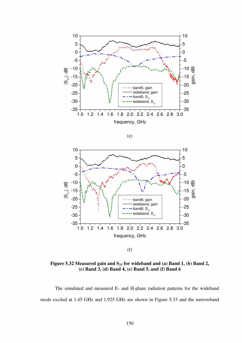
150
1.0 1.2 1.4 1.6 1.8 2.0 2.2 2.4 2.6 2.8 3.0-35
-30
-25
-20
-15
-10
-5
0
5
10
-35
-30
-25
-20
-15
-10
-5
0
5
10
ga
in,
dB
i
|S1
1|, d
B
frequency, GHz
band5, gain
wideband, gain
band5, S11
wideband, S11
(e)
1.0 1.2 1.4 1.6 1.8 2.0 2.2 2.4 2.6 2.8 3.0-35
-30
-25
-20
-15
-10
-5
0
5
10
-35
-30
-25
-20
-15
-10
-5
0
5
10
ga
in,
dB
i
|S1
1|, d
B
frequency, GHz
band6, gain
wideband, gain
band6, S11
wideband, S11
(f)
Figure 5.32 Measured gain and S11 for wideband and (a) Band 1, (b) Band 2,
(c) Band 3, (d) Band 4, (e) Band 5, and (f) Band 6
The simulated and measured E- and H-plane radiation patterns for the wideband
mode excited at 1.45 GHz and 1.925 GHz are shown in Figure 5.33 and the narrowband
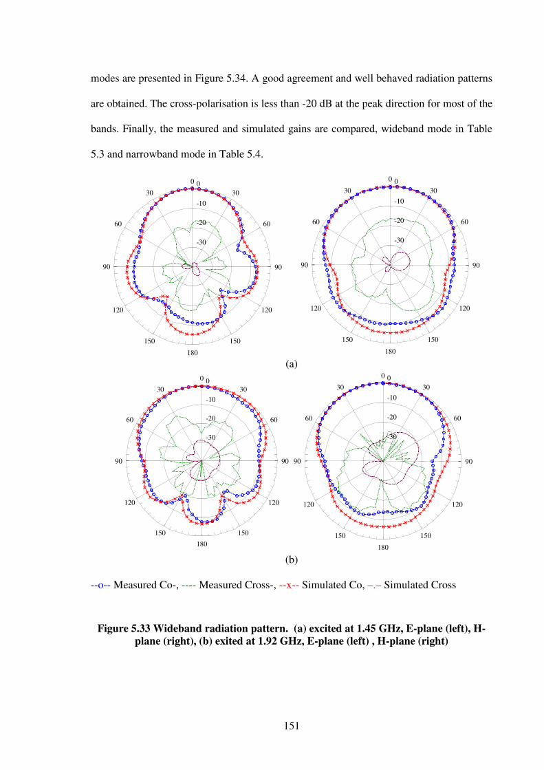
151
modes are presented in Figure 5.34. A good agreement and well behaved radiation patterns
are obtained. The cross-polarisation is less than -20 dB at the peak direction for most of the
bands. Finally, the measured and simulated gains are compared, wideband mode in Table
5.3 and narrowband mode in Table 5.4.
-30
-20
-10
0
60
120
30
150
0
180
30
150
60
120
90 90
-30
-20
-10
0
60
120
30
150
0
180
30
150
60
120
90 90
(a)
-30
-20
-10
0
60
120
30
150
0
180
30
150
60
120
90 90
-30
-20
-10
0
60
120
30
150
0
180
30
150
60
120
90 90
(b)
--o-- Measured Co-, ---- Measured Cross-, --x-- Simulated Co, –.– Simulated Cross
Figure 5.33 Wideband radiation pattern. (a) excited at 1.45 GHz, E-plane (left), H-
plane (right), (b) exited at 1.92 GHz, E-plane (left) , H-plane (right)

152
Gain in the narrowband mode is lower than in the wideband state. There are two
factors to account for the reduction in gain. One is switch loss. The other one is the change
in current distribution in the narrowband mode, which might reduce the effective aperture.
From a gain-beamwidth relationship, wider beamwidth will result in low gain. For
example, it is observed that the simulated beamwidth in the Band 6 is wider than in the
wideband mode when excited at the same frequency, 2.2 GHz. Table 5.5 shows this.
-30
-20
-10
0
60
120
30
150
0
180
30
150
60
120
90 90
-30
-20
-10
0
60
120
30
150
0
180
30
150
60
120
90 90
(a)
-30
-20
-10
0
60
120
30
150
0
180
30
150
60
120
90 90
-30
-20
-10
0
60
120
30
150
0
180
30
150
60
120
90 90
(b)

153
-30
-20
-10
0
60
120
30
150
0
180
30
150
60
120
90 90
-30
-20
-10
0
60
120
30
150
0
180
30
150
60
120
90 90
(c)
-30
-20
-10
0
60
120
30
150
0
180
30
150
60
120
90 90
-30
-20
-10
0
60
120
30
150
0
180
30
150
60
120
90 90
(d)
-30
-20
-10
0
60
120
30
150
0
180
30
150
60
120
90 90
-30
-20
-10
0
60
120
30
150
0
180
30
150
60
120
90 90
(e)
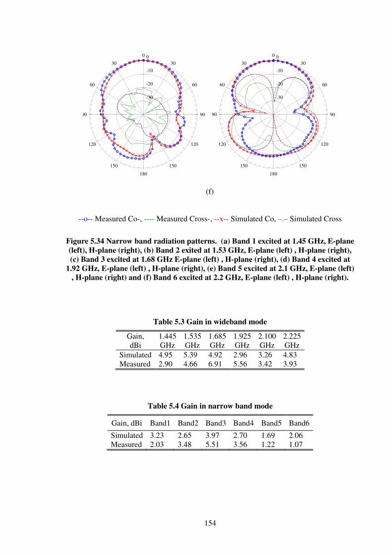
154
-30
-20
-10
0
60
120
30
150
0
180
30
150
60
120
90 90
-30
-20
-10
0
60
120
30
150
0
180
30
150
60
120
90 90
(f)
--o-- Measured Co-, ---- Measured Cross-, --x-- Simulated Co, –.– Simulated Cross
Figure 5.34 Narrow band radiation patterns. (a) Band 1 excited at 1.45 GHz, E-plane
(left), H-plane (right), (b) Band 2 exited at 1.53 GHz, E-plane (left) , H-plane (right),
(c) Band 3 excited at 1.68 GHz E-plane (left) , H-plane (right), (d) Band 4 excited at
1.92 GHz, E-plane (left) , H-plane (right), (e) Band 5 excited at 2.1 GHz, E-plane (left)
, H-plane (right) and (f) Band 6 excited at 2.2 GHz, E-plane (left) , H-plane (right).
Table 5.3 Gain in wideband mode
Gain,
dBi
1.445
GHz
1.535
GHz
1.685
GHz
1.925
GHz
2.100
GHz
2.225
GHz
Simulated 4.95 5.39 4.92 2.96 3.26 4.83
Measured 2.90 4.66 6.91 5.56 3.42 3.93
Table 5.4 Gain in narrow band mode
Gain, dBi Band1 Band2 Band3 Band4 Band5 Band6
Simulated 3.23 2.65 3.97 2.70 1.69 2.06
Measured 2.03 3.48 5.51 3.56 1.22 1.07

155
Table 5.5 Beamwidth in narrow and wideband mode at 2.2 GHz
Beamwidth, degree Band 6 Wideband
E-plane 75.4 55.7
H-plane 103.2 89.5
5.7 Summary
A new concept of switchable filtering in a Vivaldi antenna has been demonstrated.
Instead of switching between different resonator positions, the approach described here
alters the operating frequency band by varying the electrical length of the resonators
inserted into the tapered slot. This allows a better control of the operating bands but using
only two slot resonators. The narrowband operation can be switched between six different
frequency bands, which is double of what has been proposed in the multiple position ring
resonators. The example shown has good return loss for each mode and well controlled
patterns. The work described here has been published in [87]
Now it is shown that wide-narrow frequency reconfigurable Vivaldi antennas are
possible to achieve by using two methods described previously. Switching from wide to
narrowband mode provides better out of band rejection. During wideband operation, this is
not available. Therefore, it is important to provide band notch capability in order to reject
the interferer, improving the antenna versatility. In the next chapter, this will be described.

156
CHAPTER 6
VIVALDI WITH TUNABLE NARROW BAND
REJECTION
6.1 Introduction
Frequency reconfigurable antennas are useful to support many wireless
applications, where they can reduce the size of the front end circuitry and also allow some
additional receiver pre-filtering. However they are limited to one service at one time.
Wideband antennas on the other hand can support all the standards and also can operate
multiple services at a time. This is good but since they have inherently poor out of band
rejection, additional filtering is required, compromising the front end complexity. Work on
integration with fixed [38, 39, 64-67] and reconfigurable [68, 71, 72, 74] band interference
rejection filters, increasing the system versatility, have appeared in the literature.
Considering future wireless applications, for example cognitive radio, achieving a
reconfigurable band notch operation could make an important contribution to the reduction

157
in the level of interference reaching the RF front end. Reconfiguring the notch band is
useful for future cognitive radio systems where the possibility of interference between
cognitive radio users and primary users has been recognized as an expected issue causing
degradation of performance. In this chapter, a Vivaldi antenna is presented with narrow
band rejection characteristics within the 2 -7 GHz of the antenna operating bandwidth. The
tuning range is wider than that reported in [68, 71, 72, 74]. Instead of using a slot resonator
as in [39] and [38], the proposed antenna used a microstrip resonator printed on the reverse
side of the radiating element. The method, using a microstrip line resonator is proposed by
Dr F. Ghanem [10], a Research Visitor at the University of Birmingham. A significant
improvement from the original idea has been proposed. The original idea has a limited
tuning range. A new idea has been developed to achieve a tuning capability within the
whole band of operation resulting in a very wide tuning range. To give a narrow, tunable
stop band action, the resonator is loaded with varactors. Three methods are presented: one
with fixed band notching at 5.75 GHz; one with a single varactor to give a tunable band
notch between 4.2 – 5.5 GHz; and another with 3 varactors and a shorting post to the
ground, widening the stop band in the frequency range between 2 GHz and 7 GHz and
giving a tuning ratio of 3.5:1. The proposed antennas have the capability of rejecting
combinations of interfering signals (e.g. WLAN signals) within the operating bandwidth.
The design principles of the proposed antenna are described. Section 6.2 discuss the design
and the configuration of the band notch resonator within the Vivaldi space in order to
control the Q factor and the notched frequency. In section 6.3, the simulations and
experimental results are explained in detail for each method, namely fixed, narrow and
very wide tuning ranges concepts. The fabricated antenna with electronic tuning is
discussed in section 6.4, followed by a summary in section 6.5.

158
6.2 Band Notch Resonator Design
The proposed Vivaldi with band notch capability is illustrated in Figure 6.1. The
basic Vivaldi antenna was based on [82] and is similar to those described in Chapters 3 and
4 but they have been scaled down in frequency by a factor of two. The Vivaldi radiator
consists of a circular slot of 2.3 mm radius connected to an elliptical shaped tapered slot
with horizontal and vertical radius of 20 mm and 40 mm respectively. The tapered slot
ends with 15 mm radius circles. A 2.75 mm width microstrip feed line terminated with a
semi circular disk shape of 5.1 mm radius is printed on the reverse side. A Taconic TLY-5
substrate with εr = 2.2 and thickness = 0.787 mm is used. The Vivaldi covers the frequency
range from 2.0 to 7.0 GHz.
Figure 6.1 Vivaldi antenna with band notch resonator
To obtain a band notch property, a 2λ open stub microstrip resonator is printed 8.1 mm
above the feed line on the reverse side of the radiating element. The cut off band is formed
when energy from the tapered slot on the opposite side is coupled to the line resonator,

159
stopping the propagation at which the line length is 2λ . To demonstrate the concepts, an L
shaped resonator was designed and simulated.
6.2.1 Length and width of the resonator
The length of the resonator will determine the centre frequency of the notch band.
The resonator can be in any appropriate shape, such as in an L shape, proposed in this
design or in a straight line. Figure 6.2 shows the effect on S11 of the resonator in two
different lengths. L1 and the coupling point are unchanged. Clearly the centre frequency of
the notch band is length dependent. It is also observed that the Q factor is low at high
frequency indicating that the coupling factor is higher at higher frequencies. In the example
shown here, the Q is 25.625 at the low and 8.49 at the high notch band. This happens
because electrically, the centre of the coupling point is nearer to the middle point of the
resonator for the short resonator where current distribution is high as opposed to the long
resonator. Thus the coupling of the shorter resonator is higher, which produces a low Q.
However, the Q factor can be increased or decreased if required by changing the horizontal
position of the resonator as described in section 6.2.2.
The Q factor is also width dependent. Figure 6.3 shows the effect of the width, W.
Generally, the narrower is the line, the higher is the Q factor. In the example shown here,
the Q factor is 20.92, 25.32 and 29.76 for line width 1.0, 0.4 and 0.1 mm respectively. A
relatively high Q for a thin line can be understood, as the energy is confined more and
produces relatively less conductor loss. In the prototype version, a 0.4 mm width line is
chosen to relax the tolerances required in the fabrication process.

160
1.5 2.0 2.5 3.0 3.5 4.0 4.5 5.0 5.5 6.0 6.5 7.0-30
-25
-20
-15
-10
-5
0
|S1
1|, d
B
frequency, GHz
L=19 mm
L=28 mm
without resonator
Figure 6.2 Simulated S11 of antenna of Figure 6.1 with different resonator length on
band rejection centre frequency
0.90 0.95 1.00 1.05 1.10-15
-10
-5
0
|S1
1|, d
B
frequency, f/fnotch
W =1.0 mm
W =0.4 mm
W =0.1 mm
Figure 6.3 Simulated S11 of antenna of Figure 6.1 with different resonator width on
quality factor
6.2.2 Resonator positions
The effects on S11 of the resonator position in the horizontal, x-, and vertical, y-
directions are also studied. The x- and y- axes are shown in Figure 6.4. In Figure 6.5, it can
be seen that, the rejection level in the S11 is increased as a function of x-direction. It is also
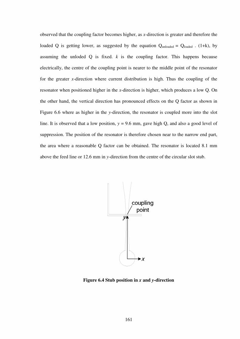
161
observed that the coupling factor becomes higher, as x-direction is greater and therefore the
loaded Q is getting lower, as suggested by the equation Qunloaded = Qloaded . (1+k), by
assuming the unloded Q is fixed. k is the coupling factor. This happens because
electrically, the centre of the coupling point is nearer to the middle point of the resonator
for the greater x-direction where current distribution is high. Thus the coupling of the
resonator when positioned higher in the x-direction is higher, which produces a low Q. On
the other hand, the vertical direction has pronounced effects on the Q factor as shown in
Figure 6.6 where as higher in the y-direction, the resonator is coupled more into the slot
line. It is observed that a low position, y = 9.6 mm, gave high Q, and also a good level of
suppression. The position of the resonator is therefore chosen near to the narrow end part,
the area where a reasonable Q factor can be obtained. The resonator is located 8.1 mm
above the feed line or 12.6 mm in y-direction from the centre of the circular slot stub.
Figure 6.4 Stub position in x and y-direction

162
1.5 2.0 2.5 3.0 3.5 4.0 4.5 5.0 5.5 6.0 6.5 7.0-30
-25
-20
-15
-10
-5
0
|S1
1|, d
B
frequency, GHz
x=0 mm
x=1.3 mm
x=2.3 mm
x=4.6 mm
Figure 6.5 S11 vs frequency for different x-positions showing the change in Q factor
1.5 2.0 2.5 3.0 3.5 4.0 4.5 5.0 5.5 6.0 6.5 7.0-30
-25
-20
-15
-10
-5
0
|S1
1|, d
B
frequency, GHz
y =17.6 mm
y =12.6 mm
y =9.6 mm
Figure 6.6 S11 vs frequency for different y-positions showing the change in Q factor
6.2.3 Varactor positions
To tune the centre frequency of the rejection band, it is appropriate to locate a
varactor in the middle of the resonator. This is the optimum position for maximising the
tuning range, because the maximum differential voltage can be established across the
diode. Figure 6.7 shows current distributions on the resonator excited at the notch

163
frequency of 5.73 GHz. It is observed that the current is high in the middle of the line.
Figure 6.8a shows the effect of varactor position in the line, showing that a tuning range of
680 MHz is achieved when the varactor is in the middle. Using the same values of the
capacitances, the tuning range is slightly smaller at 364 MHz when it is ¼ of the line
length away from the mid point of the resonator as shown in Figure 6.8b. It can be
observed that the line gap is approximately short circuit when the varactor is set higher
than 5.6 pF. The centre frequency of the notch band has a small effect on the capacitance
above 5.6 pF as shown in Figure 6.9.
Figure 6.7 Current distribution in the resonator at notch frequency of 5.73 GHz
1.5 2.0 2.5 3.0 3.5 4.0 4.5 5.0 5.5 6.0 6.5 7.0-30
-25
-20
-15
-10
-5
0
R=680 MHz
|S1
1|, d
B
frequency, GHz
0.5pF
0.7pF
1.5pF
5.6pF
(a)
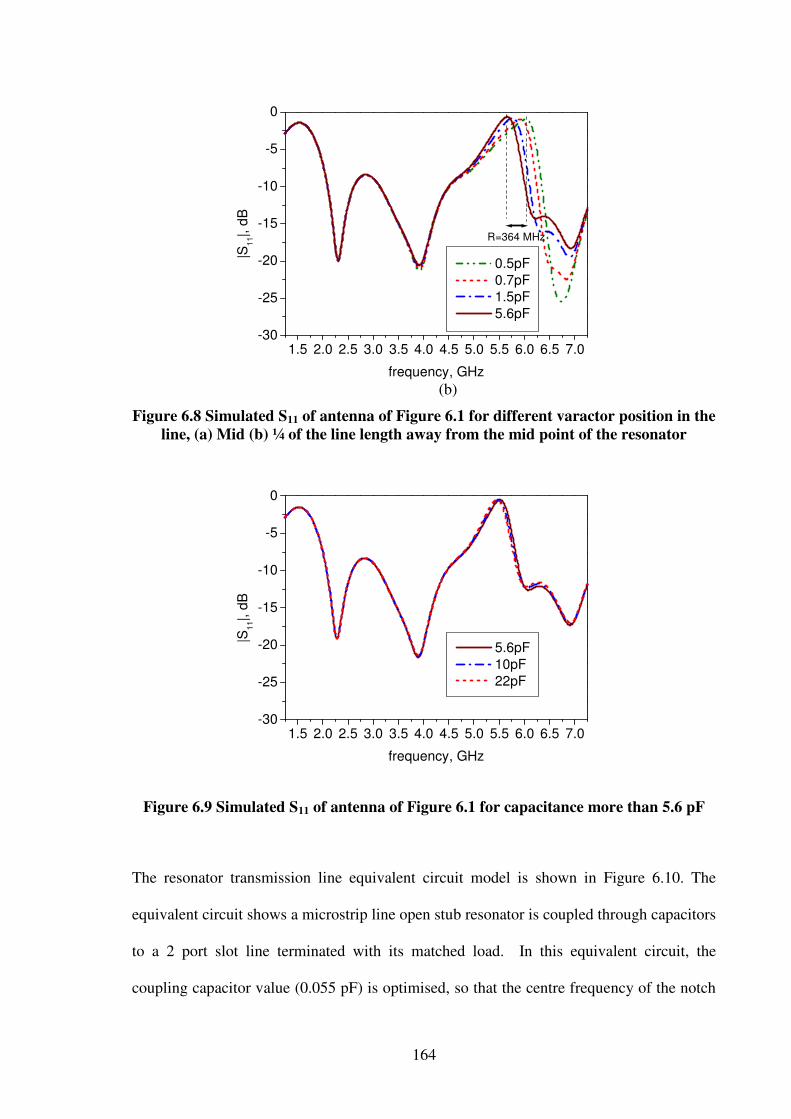
164
1.5 2.0 2.5 3.0 3.5 4.0 4.5 5.0 5.5 6.0 6.5 7.0-30
-25
-20
-15
-10
-5
0
R=364 MHz
|S1
1|, d
B
frequency, GHz
0.5pF
0.7pF
1.5pF
5.6pF
(b)
Figure 6.8 Simulated S11 of antenna of Figure 6.1 for different varactor position in the
line, (a) Mid (b) ¼ of the line length away from the mid point of the resonator
1.5 2.0 2.5 3.0 3.5 4.0 4.5 5.0 5.5 6.0 6.5 7.0-30
-25
-20
-15
-10
-5
0
|S1
1|, d
B
frequency, GHz
5.6pF
10pF
22pF
Figure 6.9 Simulated S11 of antenna of Figure 6.1 for capacitance more than 5.6 pF
The resonator transmission line equivalent circuit model is shown in Figure 6.10. The
equivalent circuit shows a microstrip line open stub resonator is coupled through capacitors
to a 2 port slot line terminated with its matched load. In this equivalent circuit, the
coupling capacitor value (0.055 pF) is optimised, so that the centre frequency of the notch

165
band is approximately the same with the result obtained from full wave EM simulation.
The objectives of this equivalent circuit are to show in general how changing the
capacitance will change the centre of the resonant frequency and the Q factor. The
equivalent circuit shown in Figure 6.10 approximately describes the resonator explained in
section 6.3.2.
Figure 6.10 Resonator equivalent circuit
Figure 6.11a and Figure 6.11b show the s-parameters when the capacitor is set to
0.1 pF and 5.6 pF respectively. The corresponding VSWR is shown in Figure 6.12. When
changing the capacitance values, the resonant frequency is also changed and the Q factor is
increased at low frequency. This is presumably because, electrically the centre of the

166
resonator moves outward from the coupling point when the line is electrically longer and
this therefore reduces the coupling. The coupling can also be observed through VSWR,
where higher standing wave ratio shows high coupling.
2 3 4 5 6 7 8-30
-25
-20
-15
-10
-5
0
s-p
ara
me
ters
, d
B
frequency, GHz
S11
S21
(a)
2 3 4 5 6 7 8-30
-25
-20
-15
-10
-5
0
s-p
ara
me
ters
, dB
frequency, GHz
S11
S21
(b)
Figure 6.11 S-parameters of equivalent circuit of the resonator when capacitor is set
to (a) 0.1 pF, (b) 5.6 pF
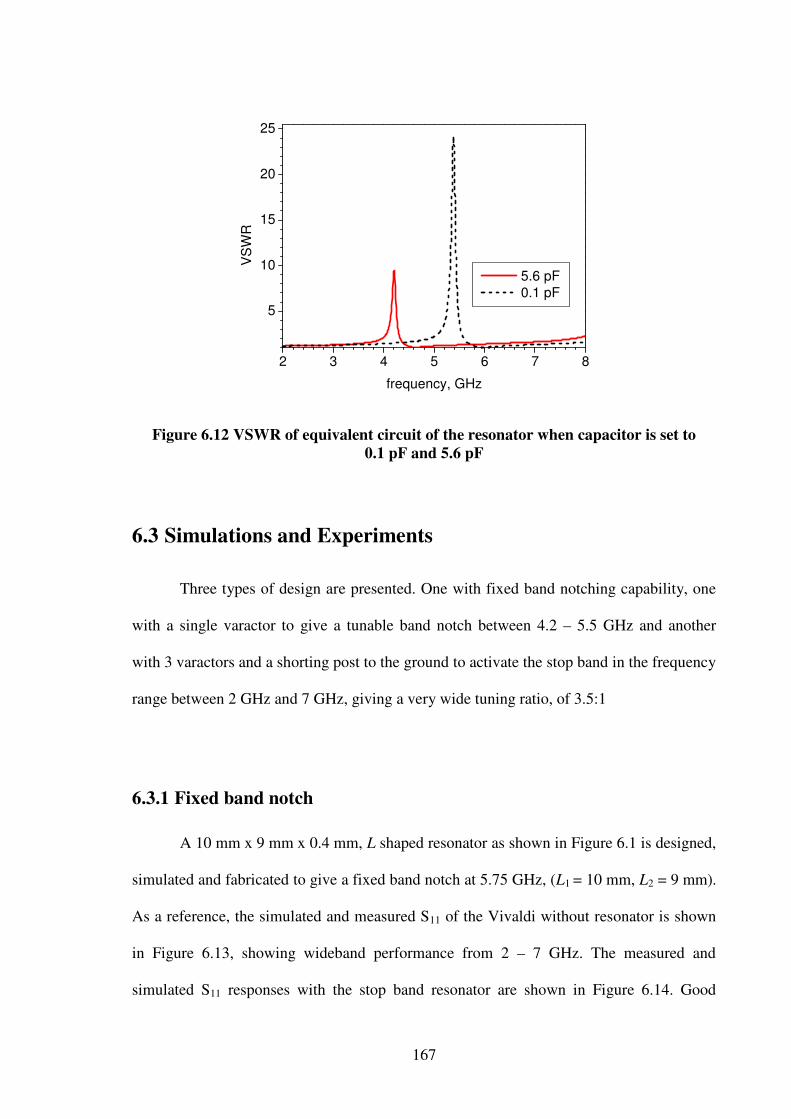
167
2 3 4 5 6 7 8
5
10
15
20
25
VS
WR
frequency, GHz
5.6 pF
0.1 pF
Figure 6.12 VSWR of equivalent circuit of the resonator when capacitor is set to
0.1 pF and 5.6 pF
6.3 Simulations and Experiments
Three types of design are presented. One with fixed band notching capability, one
with a single varactor to give a tunable band notch between 4.2 – 5.5 GHz and another
with 3 varactors and a shorting post to the ground to activate the stop band in the frequency
range between 2 GHz and 7 GHz, giving a very wide tuning ratio, of 3.5:1
6.3.1 Fixed band notch
A 10 mm x 9 mm x 0.4 mm, L shaped resonator as shown in Figure 6.1 is designed,
simulated and fabricated to give a fixed band notch at 5.75 GHz, (L1 = 10 mm, L2 = 9 mm).
As a reference, the simulated and measured S11 of the Vivaldi without resonator is shown
in Figure 6.13, showing wideband performance from 2 – 7 GHz. The measured and
simulated S11 responses with the stop band resonator are shown in Figure 6.14. Good
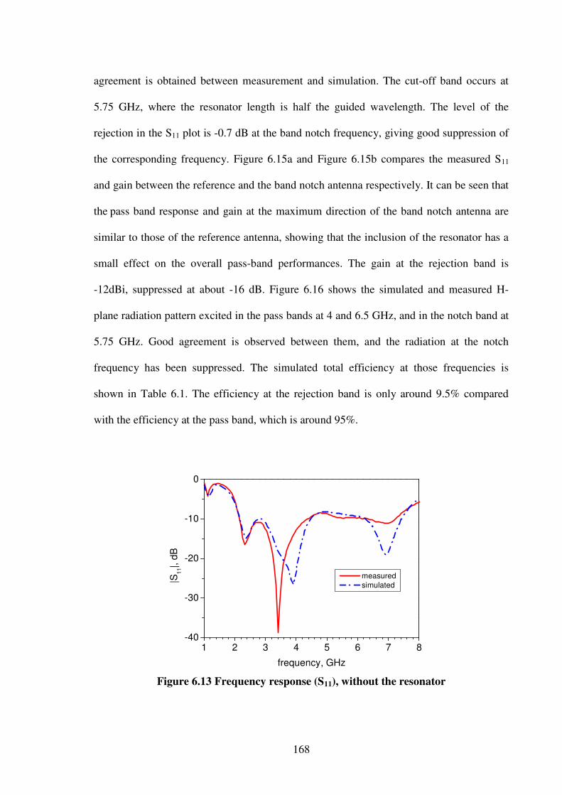
168
agreement is obtained between measurement and simulation. The cut-off band occurs at
5.75 GHz, where the resonator length is half the guided wavelength. The level of the
rejection in the S11 plot is -0.7 dB at the band notch frequency, giving good suppression of
the corresponding frequency. Figure 6.15a and Figure 6.15b compares the measured S11
and gain between the reference and the band notch antenna respectively. It can be seen that
the pass band response and gain at the maximum direction of the band notch antenna are
similar to those of the reference antenna, showing that the inclusion of the resonator has a
small effect on the overall pass-band performances. The gain at the rejection band is
-12dBi, suppressed at about -16 dB. Figure 6.16 shows the simulated and measured H-
plane radiation pattern excited in the pass bands at 4 and 6.5 GHz, and in the notch band at
5.75 GHz. Good agreement is observed between them, and the radiation at the notch
frequency has been suppressed. The simulated total efficiency at those frequencies is
shown in Table 6.1. The efficiency at the rejection band is only around 9.5% compared
with the efficiency at the pass band, which is around 95%.
1 2 3 4 5 6 7 8-40
-30
-20
-10
0
|S1
1|, d
B
frequency, GHz
measured
simulated
Figure 6.13 Frequency response (S11), without the resonator

169
1 2 3 4 5 6 7 8-30
-25
-20
-15
-10
-5
0
|S1
1|,d
B
frequency, GHz
measured
simulated
Figure 6.14 S11 characteristic of the antenna with stop-band resonator
1 2 3 4 5 6 7 8-30
-25
-20
-15
-10
-5
0
|S1
1|,d
B
frequency, GHz
notch band
wideband
(a)

170
1 2 3 4 5 6 7 8
-14
-12
-10
-8
-6
-4
-2
0
2
4
6
8
ga
in,
dB
i
frequency, GHz
notch band
wideband
(b)
Figure 6.15 Band notch and reference antenna performances, (a) S11, and (b) gain
-30
-20
-10
0
10
60
120
30
150
0
180
30
150
60
120
90 90
(a)

171
-30
-20
-10
0
10
60
120
30
150
0
180
30
150
60
120
90 90
(b)
Figure 6.16 H-plane radiation pattern excited at pass band at 4 and 6.5 GHz, and
notch band at 5.75 GHz, (a) simulated, and (b) measured
Table 6.1 Simulated total efficiency
Frequency (GHz) 4.0 6.5 5.75
Total efficiency (%) 97.35 95.53 9.57
6.3.2 Tunable Notch
The antenna concepts in this section is contributed by Dr F. Ghanem [10] and
included to ensure continuity in the description of the new antenna. The simulation,
measurement and the analysis of this section however are done by the author of this thesis.

172
A 10 mm (L1) x 18 mm (L2) x 0.4 mm L shaped resonator as shown in Figure 6.10 is
designed and simulated. A 1 mm gap used to locate the capacitor is created 8 mm from the
top of the microstrip resonator to give a tunable band notch between 4.2 – 5.5 GHz.
Prototypes with different fixed capacitors are developed to verify the proposed concepts.
Five capacitors with values from 5.6, 1.1, 0.5, 0.2, and 0.1 pF were used. The range of
these capacitors can approximately be obtained from Microsemi varactor MV31013 (0.15 –
6.25 pF) or MV34001 (0.1 – 4.5 pF). The measured and simulated S11 responses with the
stop-band are shown in Figure 6.17a and Figure 6.17b respectively. It is demonstrated that
the stop-band at 4.2 to 5.5 GHz appears within the 2 – 7 GHz operating band. Figure 6.18
compares the measured and simulated S11 when capacitance of 0.1 pF is used. The
corresponding gain is shown in Figure 6.19. A good agreement is observed, where the
main features are well predicted. Measured gains at other stop-band are shown in Figure
6.20. The gain is suppressed significantly at about -11 to -14 dB in the stop band. On the
whole, the lower and upper pass-band gains follows similar trends as compared with non-
stop band version as shown in Figure 6.21. Figure 6.22 shows the simulated radiation
pattern of the proposed antenna excited at pass band 4.5 GHz and 6 GHz, and notch band
at 5.46 GHz. The radiated power has clearly dropped, by about -14 dB, in the notch band at
5.46 GHz compared to in the pass-band at 6 GHz and 4.5 GHz. The measured radiation
pattern excited at pass-band 4.5 GHz and 6 GHz, and notch-band at 5.32 GHz is shown in
Figure 6.23. Similar behaviour is observed.

173
1.5 2.0 2.5 3.0 3.5 4.0 4.5 5.0 5.5 6.0 6.5 7.0-30
-25
-20
-15
-10
-5
0
|S1
1|, d
B
frequency, GHz
5.6pF
1.1pF
0.5pF
0.2pF
0.1pF
(a)
1.5 2.0 2.5 3.0 3.5 4.0 4.5 5.0 5.5 6.0 6.5 7.0-30
-25
-20
-15
-10
-5
0
|S1
1|, d
B
frequency, GHz
5.6pF
1.1pF
0.5pF
0.2pF
0.1pF
(b)
Figure 6.17 S11 responses, (a) measured, (b) simulated

174
1.5 2.0 2.5 3.0 3.5 4.0 4.5 5.0 5.5 6.0 6.5 7.0-30
-25
-20
-15
-10
-5
0
|S1
1|, d
B
frequency, GHz
measured
simulated
Figure 6.18 S11 responses with 0.1 pF capacitance
2.0 2.5 3.0 3.5 4.0 4.5 5.0 5.5 6.0 6.5 7.0 7.5 8.0
-10
-8
-6
-4
-2
0
2
4
6
8
ga
in,
dB
i
frequency, GHz
measured
simulated
Figure 6.19 Gain with 0.1 pF capacitance

175
2.0 2.5 3.0 3.5 4.0 4.5 5.0 5.5 6.0 6.5 7.0-12
-10
-8
-6
-4
-2
0
2
4
6
8
ga
in,
dB
i
frequency, GHz
5.6pF
1.1pF
0.5pF
0.2pF
0.1pF
Figure 6.20 Measured gain of the proposed antenna with fixed capacitors
2.0 2.5 3.0 3.5 4.0 4.5 5.0 5.5 6.0 6.5 7.0-10
-8
-6
-4
-2
0
2
4
6
8
ga
in,
dB
i
frequency, GHz
wideband
notch band
Figure 6.21 Antenna gain without resonator and with resonator using 0.1 pF

176
Figure 6.22 Simulated E-plane radiation pattern excited at pass band at 4.5 and 6
GHz, and notch band at 5.46 GHz
-30
-20
-10
0
10
60
120
30
150
0
180
30
150
60
120
90 90
Figure 6.23 Measured E-plane radiation pattern excited at pass band at 4.5 and 6
GHz, and notch band at 5.32 GHz
-30
-20
-10
0
10
60
120
30
150
0
180
30
150
60
120
90 90

177
This part ends the contribution of Dr F. Ghanem on this work.
6.3.3 Multiple Varactor for Wider Tuning Range
To achieve a very wide tuning range, the resonator has been divided into three
sections using small gaps as shown in Figure 6.24. The stop band centre frequency will
therefore be determined by the active total length. Three varactors are used. Two varactors,
C1 and C2, are used to bridge the 1 mm gaps in the resonator. At the top end, a third
varactor, C3, is used to bridge the gap between the resonator and a shorting post to the
ground. The varactors are used to vary the resonator impedance and hence effectively tune
the stop band centre frequency. When the varactors are tuned to more than 5.6 pF or to
their minimum capacitance of 0.1 pF, the gap in the line will approximate to a short or
open circuit, respectively. Using a combination of shorts or opens at the gaps, three
different sets of active resonator lengths, L1, L2 and 2L2, can be obtained.
Figure 6.24 Proposed resonator with three gaps

178
The varactor settings for these are now described. To create the L1 section, as the
only active resonator, the three varactors, C1, C2 and C3 are set to 5.6 pF, 0.1 pF and 0.1 pF
respectively. Ideally, with L1 = 19 mm, the length is approximately half a wavelength long
at 5.75 GHz. However with the addition of the capacitors the actual electrical length of L1
has been elongated so that the stop band now occurs at 4.9 GHz. The stop bands in the
higher band between 4.9 to 6.8 GHz can be achieved when C1 is tuned between 5.6 to 0.14
pF. On the other hand, to make the L2 section, as the active resonator, the three varactors,
C1, C2 and C3 are set to 5.6 pF, 5.6 pF and 0.1 pF respectively. This makes the length of L2
approximately half a wavelength at 3.5 GHz. Stop bands in the middle band between 3.5 to
4.8 GHz are obtained by varying C2 between 5.6 to 0.15 pF. Finally, to obtain the L2
section with a short circuit at the end, C3 is set to 5.6 pF which effectively creates L2 as a
short circuit stub of length 900 at 1.8 GHz. Changing C2 between 5.6 to 0.1 pF, the band
stop centre frequency is tuned to a lower band between 2.1 and 4.2 GHz. Because the
effective length is now longer, a third harmonic occurs at around 5.7 GHz. Nevertheless,
the length is designed so that the band rejection at the third harmonic occurs at the WLAN
frequency, around 5.7 GHz. Also, the varactor, C2 has been positioned in the line where the
current at the third harmonic frequency is zero as shown in Figure 6.25. Thus the 5.7 GHz
stop band does not change with C2.
Various fixed capacitors are used to represent varactors in the simulation and also
in the fabricated antenna. The simulated S11 showing various tunable stop bands at
different frequencies denoted as (m1-m5) when 2L2 is activated, (m6-m10) when L2 is
activated and (m11-m17) when L1 is activated, are presented in Figure 6.26a, Figure 6.26b
and Figure 6.26c respectively. Figure 6.27 shows all the notch bands. It is clearly seen that
the stop band can be tuned between 2 – 7 GHz using the proposed concepts by activating
three different resonator lengths. Table 6.2 give the capacitor values for these frequencies.

179
Figure 6.25 Current distribution at the third harmonic frequency showing current
zero occurs at varactor C2 position
1 2 3 4 5 6 7-30
-25
-20
-15
-10
-5
0
|S11|, d
B
frequency, GHz
m1 m2 m3 m4 m5
(a)

180
1 2 3 4 5 6 7-30
-25
-20
-15
-10
-5
0
|S11|, d
B
frequency, GHz
m6 m7 m8 m9 m10
(b)
1 2 3 4 5 6 7-30
-25
-20
-15
-10
-5
0
|S11|, d
B
frequency, GHz
m10 m11 m12 m13
m14 m16 m17
(c)
Figure 6.26 Simulated notch band frequency response (S11), (a) 2L2-(m1-m5), (b) L2-
(m6-m10), (c) L1-(m11-m17) active
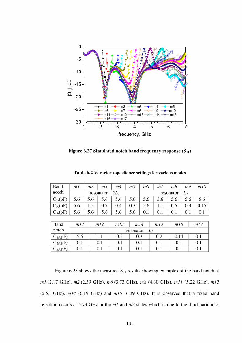
181
1 2 3 4 5 6 7-30
-25
-20
-15
-10
-5
0
|S11|, d
B
frequency, GHz
m1 m2 m3 m4 m5
m6 m7 m8 m9 m10
m11 m12 m13 m14 m15
m16 m17
Figure 6.27 Simulated notch band frequency response (S11)
Table 6.2 Varactor capacitance settings for various modes
Band
notch
m1 m2 m3 m4 m5 m6 m7 m8 m9 m10
resonator – 2L2 resonator – L2
C1,(pF) 5.6 5.6 5.6 5.6 5.6 5.6 5.6 5.6 5.6 5.6
C2,(pF) 5.6 1.5 0.7 0.4 0.3 5.6 1.1 0.5 0.3 0.15
C3,(pF) 5.6 5.6 5.6 5.6 5.6 0.1 0.1 0.1 0.1 0.1
Band
notch
m11 m12 m13 m14 m15 m16 m17
resonator – L1
C1,(pF) 5.6 1.1 0.5 0.3 0.2 0.14 0.1
C2,(pF) 0.1 0.1 0.1 0.1 0.1 0.1 0.1
C3,(pF) 0.1 0.1 0.1 0.1 0.1 0.1 0.1
Figure 6.28 shows the measured S11 results showing examples of the band notch at
m1 (2.17 GHz), m2 (2.39 GHz), m6 (3.73 GHz), m8 (4.30 GHz), m11 (5.22 GHz), m12
(5.53 GHz), m14 (6.19 GHz) and m15 (6.39 GHz). It is observed that a fixed band
rejection occurs at 5.73 GHz in the m1 and m2 states which is due to the third harmonic.
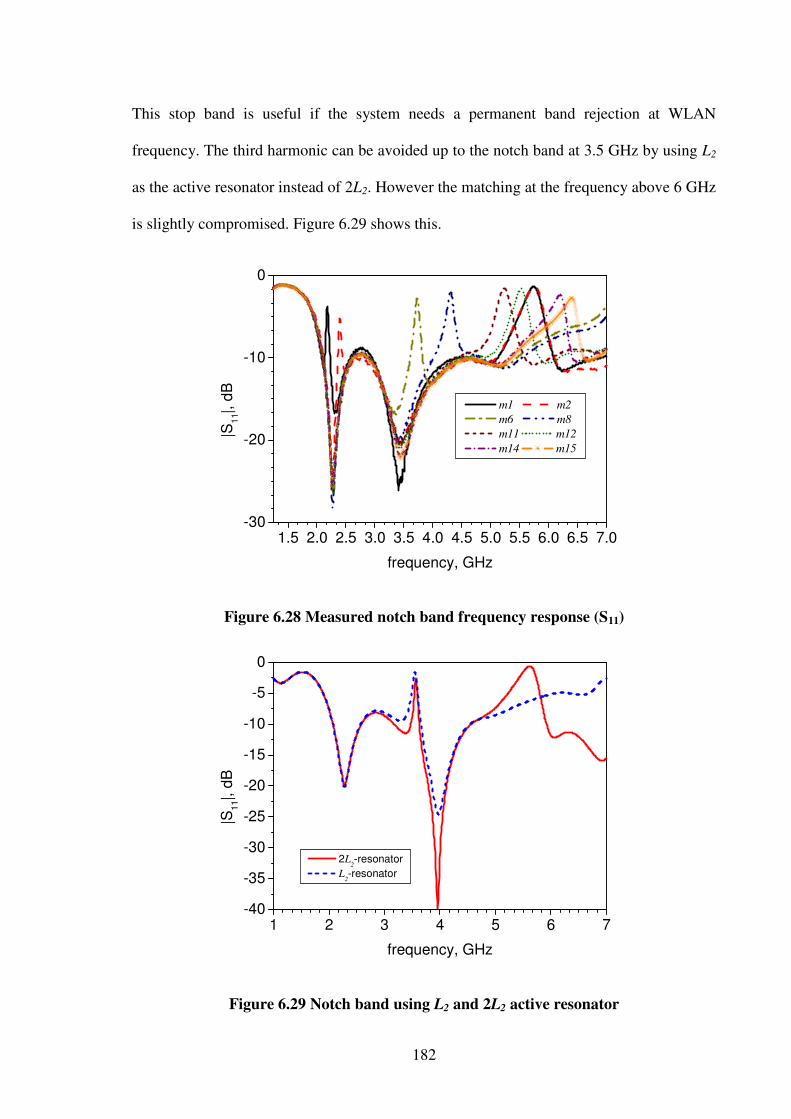
182
This stop band is useful if the system needs a permanent band rejection at WLAN
frequency. The third harmonic can be avoided up to the notch band at 3.5 GHz by using L2
as the active resonator instead of 2L2. However the matching at the frequency above 6 GHz
is slightly compromised. Figure 6.29 shows this.
1.5 2.0 2.5 3.0 3.5 4.0 4.5 5.0 5.5 6.0 6.5 7.0-30
-20
-10
0
|S1
1|, d
B
frequency, GHz
m1 m2
m6 m8
m11 m12
m14 m15
Figure 6.28 Measured notch band frequency response (S11)
1 2 3 4 5 6 7-40
-35
-30
-25
-20
-15
-10
-5
0
|S1
1|, d
B
frequency, GHz
2L2-resonator
L2-resonator
Figure 6.29 Notch band using L2 and 2L2 active resonator

183
The measured gain for m1, m2, m4, m6, m8, m11, m12, m14 and m15 is shown in
Figure 6.30. It is clearly seen that sharp gain reduction occurs in every stop band ranging
between -7 and -16 dB. The measured E-plane radiation pattern excited at 2.18 GHz (m1)
and 4.30 GHz (m8) before and after notching is shown in Figure 6.31. The gain is
suppressed by about -10 dB in m1 and -12 dB in m8 operations. Figure 6.32 shows the
measured radiation pattern of m1 mode excited in the pass band at 4.3 and 6.18 GHz, and
in the notch bands at 2.18 and 5.78 GHz. The radiated power is clearly seen to have
dropped, by about -14 dB, in the notch band at 2.18 GHz and -18 dB at 5.78 GHz
compared to in the pass band at 4.3 GHz and 6.18 GHz. The simulated radiation pattern
excited in the pass band at 4.3 and 6.18 GHz, and in the notch bands at 2.18 and 5.78 GHz
is shown in Figure 6.33. Similar behaviour is observed.
2 3 4 5 6 7
-12
-10
-8
-6
-4
-2
0
2
4
6
8
ga
in,
dB
i
frequency, GHz
m1 m2 m4
m6 m8 m11
m12 m14 m15
wide
Figure 6.30 Measured gain
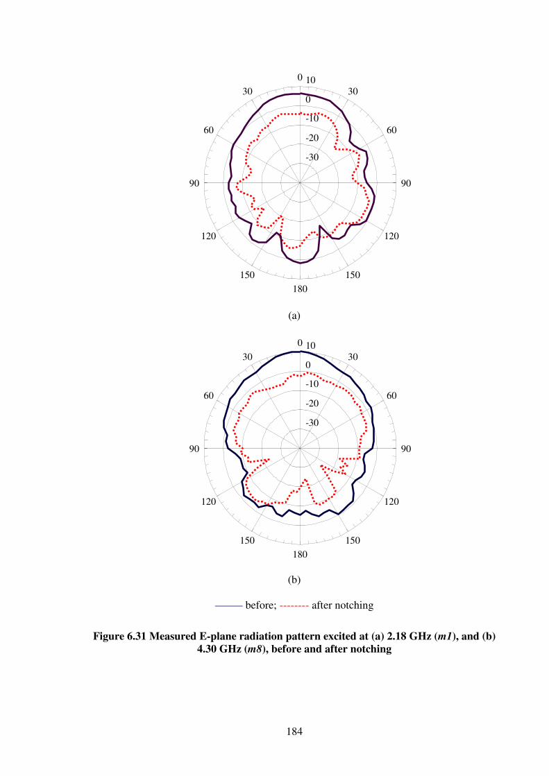
184
-30
-20
-10
0
10
60
120
30
150
0
180
30
150
60
120
90 90
(a)
-30
-20
-10
0
10
60
120
30
150
0
180
30
150
60
120
90 90
(b)
––––– before; -------- after notching
Figure 6.31 Measured E-plane radiation pattern excited at (a) 2.18 GHz (m1), and (b)
4.30 GHz (m8), before and after notching

185
-30
-20
-10
0
10
60
120
30
150
0
180
30
150
60
120
90 90
Figure 6.32 Measured E-plane radiation pattern in m1 mode excited at pass band at
4.3 and 6.18 GHz, and notch band at 2.18 and 5.78 GHz
-30
-20
-10
0
10
60
120
30
150
0
180
30
150
60
120
90 90
Figure 6.33 Simulated E-plane radiation pattern in m1 mode excited at pass band at
4.3 and 6.18 GHz, and notch band at 2.2 and 5.89 GHz
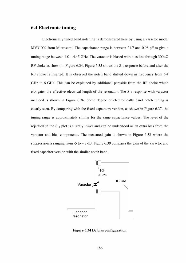
186
6.4 Electronic tuning
Electronically tuned band notching is demonstrated here by using a varactor model
MV31009 from Microsemi. The capacitance range is between 21.7 and 0.98 pF to give a
tuning range between 4.0 – 4.45 GHz. The varactor is biased with bias line through 300kΩ
RF choke as shown in Figure 6.34. Figure 6.35 shows the S11 response before and after the
RF choke is inserted. It is observed the notch band shifted down in frequency from 6.4
GHz to 6 GHz. This can be explained by additional parasitic from the RF choke which
elongates the effective electrical length of the resonator. The S11 response with varactor
included is shown in Figure 6.36. Some degree of electronically band notch tuning is
clearly seen. By comparing with the fixed capacitors version, as shown in Figure 6.37, the
tuning range is approximately similar for the same capacitance values. The level of the
rejection in the S11 plot is slightly lower and can be understood as an extra loss from the
varactor and bias components. The measured gain is shown in Figure 6.38 where the
suppression is ranging from -5 to – 8 dB. Figure 6.39 compares the gain of the varactor and
fixed capacitor version with the similar notch band.
Figure 6.34 Dc bias configuration
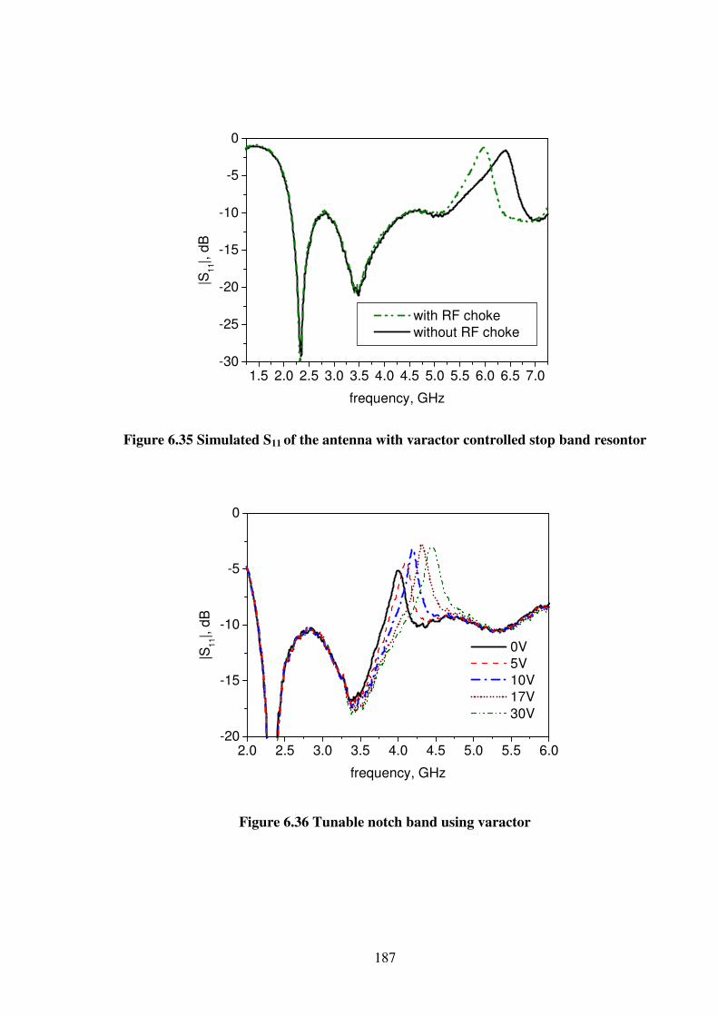
187
1.5 2.0 2.5 3.0 3.5 4.0 4.5 5.0 5.5 6.0 6.5 7.0-30
-25
-20
-15
-10
-5
0
|S1
1|, d
B
frequency, GHz
with RF choke
without RF choke
Figure 6.35 Simulated S11 of the antenna with varactor controlled stop band resontor
2.0 2.5 3.0 3.5 4.0 4.5 5.0 5.5 6.0-20
-15
-10
-5
0
|S1
1|, d
B
frequency, GHz
0V
5V
10V
17V
30V
Figure 6.36 Tunable notch band using varactor

188
2.0 2.5 3.0 3.5 4.0 4.5 5.0 5.5 6.0-20
-15
-10
-5
0
|S1
1|, d
B
frequency, GHz
Varactor, 10V
Fixed capacitor, 5.6pF
Figure 6.37 S11 plot with varactor and fixed capacitor
2.0 2.5 3.0 3.5 4.0 4.5 5.0 5.5 6.0-5
-4
-3
-2
-1
0
1
2
3
4
5
ga
in,
dB
i
frequency, GHz
10V
17V
25V
Figure 6.38 Measured gain of the proposed antenna with varactor

189
2.0 2.5 3.0 3.5 4.0 4.5 5.0 5.5 6.0 6.5 7.0
-10
-8
-6
-4
-2
0
2
4
6
8
gain
, dB
i
frequency, GHz
Varactor(17V)
Fixed capacitor(1.1pF)
Figure 6.39 Varactor and fixed capacitor on gain
6.5 Summary
To realize a band notch capability in a Vivaldi antenna, a microstrip line resonator
has been integrated to prevent the propagation of signals in the frequency notch band.
Three methods have been demonstrated. In the first method, a 19 mm length resonator is
used to stop the propagation at 5.75 GHz band. In the second method, some degree of
tunable band notching is achieved, using a 28 mm length resonator and a single varactor.
The third method shows a very high tuning range using the same length of the resonator
and three varactors and a shorting post to the ground. The advantage of the proposed band
rejection method here in which the resonator is integrated within the antenna space, is that
it has a very minimal effect on the gain performances in the pass bands. The pass band
response in gain and S11 is very similar to that reference antenna (i.e. without resonator).
Furthermore the tuning range can be extended by elongating the electrical length of the

190
resonator. A tunable band notch antenna has been developed and tested. The performance
shown verifies the proposed design concept. This work has been reported in [75, 88].

191
CHAPTER 7
COMBINED WIDE-NARROW-NOTCH BAND
VIVALDI ANTENNA
7.1 Introduction
Multimode radio, UWB system and future cognitive radio pose considerable
challenges for antenna designer. Many novel reconfigurable antennas and UWB antennas
have appeared in the literature. In the three previous chapters two combined wideband-
narrowband Vivaldi antennas and a wideband with tunable band notch have been
described. Also most of the reconfigurable antennas reported so far have only a two mode
capability, either reconfiguring from one narrowband to another narrowband [2], a
wideband to a notch band [69] or a wideband to narrowband [7]. However, to the best of
our knowledge, no attempt has yet been reported to combine three modes, namely
wideband, notch, narrowband, in one single antenna. In this chapter we propose a novel
multi-function Vivaldi antenna with the capability to switch between wideband, notch band
192
and narrowband mode by combining the concepts described in chapter 5 and 6
respectively. The antenna in a wideband mode is designed to have a bandwidth of
2 – 8 GHz. In the notch band mode, the antenna has tunable narrowband rejection between
5.2 GHz and 5.7 GHz. The Vivaldi can also operate in a narrow pass band modes centred
on 3.6, 3.9, 4.8, 5.5 and 6.5 GHz. The notch band reconfiguration is realized by
incorporating a microstrip line resonator across the tapered slot on the opposite side of the
substrate. The resonator can be deactivated to obtain the wideband mode. The narrowband
operation is realized by inserting a pair of ring slots into the radiating element. Measured
and simulated results are presented. Details of the proposed design are described. Antenna
design is explained in section 7.2. In section 7.3, the antenna operations and simulation
and measurement results are discussed. Finally the conclusions are presented in section
7.4.
7.2 Antenna Design
A planar Vivaldi with a tapered slot profile shown in Figure 7.1 is designed on
Taconic TLY-5 substrate with rε = 2.2. The size and geometry of the basic Vivaldi
antenna are similar as described in Chapter 6.
Two types of resonators have been incorporated into the Vivaldi structure. First, a
Z shaped 0.4 mm width microstrip line resonator is located on the reverse side of the slot in
order to create a band rejection mode. The resonator is located 6.7 mm above the feed line
as shown in Fig 1(b). The resonator is placed in the transmission line region in the lower
throat. The microstrip line resonator (L1 + L2) acts as an open stub and has 22.3 mm length.
It has a gap, bridged by a variable capacitor, placed at distance L1 = 6 mm from the left end
to obtain a tunable band notch mode. L1 is chosen to be 6 mm so that the notch band will

193
be considerably weak (low coupling to L2) when capacitance is set to 0.1 pF. A weak band
rejection is useful to deactivate the effect of the resonator which is described later.
(a) (b)
Figure 7.1 Antenna configuration (a) Front view, (b) Rear view
To obtain the wideband mode, the band notch element has to be deactivated. They
are sometimes effectively switched off by simply shifting them out of band. Due to the
wide bandwidth of this antenna, it has not been done here. Instead, the band notch is turned
off by connecting a resistor to the resonator.
To obtain the other function, a narrow pass band, a second resonator consisting of a
pair of ring slots is inserted into the radiating element. The centre of the ring slot is 14.62
mm above the center of circular slot stub. Similarly to the microstrip line resonator, the
ring slot is also placed at the lower throat of the tapered slot. The ring slot has an inner
radius of 4 mm and outer radius of 6 mm. Switches are positioned at specific locations.
Variation of the pass band response is achieved by setting up switch combinations as
shown in Figure 7.2. In the microstrip resonator, fixed capacitors are used to represent the
varactor. Metal pads of size 0.5 mm x 2 mm are used to represent the switches, such that

194
the presence and absence of the metal pad represents on and off states respectively. A
prototype with ideal switches and fixed capacitors has been developed and tested. A
prototype of the Vivaldi antenna with the ring slots and real switches but without the new
notch tuning capability is described in detail in Chapter 5 and reported in [87].
Switch location and Pass band
Band1 3.6 GHz
Band4 5.5 GHz
Band2 3.9 GHz
Band5 6.5 GHz
Band3 4.8 GHz
Wideband
Figure 7.2 Pass band switch configuration
7.3 Antenna Operations and Results
A wideband mode is achieved after the ring slots are decoupled from the tapered
slot by short circuiting the small gaps connecting them to the slot, whilst the capacitors on
the microstrip line resonator are set to 0.1 pF and the resistive load is connected to switch
off the notch. To deactivate the resonator, the capacitor is tuned to 0.1 pF, which
electrically shortens the resonator and consequently reduces the coupling between L1 and
L2. A low coupling between L1 and L2 reflects a weak notch. Figure 7.3 shows this, where a
weak notch band is observed and the centre frequency of the band notch is approximately

195
corresponding to length L2. With the weak notch, its effects can be easily removed by
adding a resistive load at the other end via a PIN diode switch, which will change the
standing wave at the coupling point. The resistor helps further to remove the notch band
when the diode is in the on state. Because of the resistor location, only small current will
flow through them. Figure 7.4 shows the effects of the notch band as a function of resistor
value. By increasing the resistance, the unloaded Q is expected to be low and presumably
the standing wave will also become low at the coupling point and this will probably reduce
further the coupling factor. From parametric study, it was found that the notch band is
removed completely when a 100 Ω resistor is used. A wide bandwidth of 2 – 8 GHz is
achieved. Figure 7.5 shows the measured and simulated S11 in a wideband mode. Good
agreement is observed. The measured S11 and the measured gain before and after the 100 Ω
resistor is connected are shown in Figure 7.6 and Figure 7.7 respectively. Also compared
in that Figure 7.7 is the reference antenna (without z-shaped and ring slot resonator). The
notch effect from the gain suppression is removed after the resistive load is added and yet
the gain is comparable with the reference gain.
To show how the resistive load helps in removing the notch effects, an equivalent
circuit shown in Figure 7.8 (notes: given in previous chapter) is constructed. Figure 7.9 and
Figure 7.10 compares the s-parameters and VSWR respectively, for a case when a 100 Ω
resistor is connected or disconnected from the line. The capacitance is set to 0.1 pF. The
stop band is reduced where the S11 is below -10 dB throughout the band. The VSWR is less
than 2 for R = 100 Ω, indicating the coupling to the slot is very small, and therefore the
resonator is effectively switched off hence killing the notch band and providing a
wideband mode.

196
2 3 4 5 6 7 8
-30
-20
-10
0
|S1
1|, d
B
frequency, GHz
Meas
Sim
Figure 7.3 Frequency notch using 0.1 pF
5.0 5.5 6.0 6.5 7.0
-14
-12
-10
-8
|S11|, d
B
frequency, GHz
3 Ω
15 Ω
30 Ω
100 Ω
Figure 7.4 The effects of the notch band as a function of resistor value

197
2 3 4 5 6 7 8-40
-30
-20
-10
0
|S11|, d
B
frequency, GHz
Measured Simulated
Figure 7.5 Wideband mode response
2 3 4 5 6 7 8-30
-20
-10
0
|S11|, d
B
frequency, GHz
with 100 Ω
without 100 Ω
Figure 7.6 Measured S11 with and without 100 ΩΩΩΩ

198
2 3 4 5 6 7 8
-4
-2
0
2
4
6
8
ga
in, d
Bi
frequency, GHz
without 100 Ω
with 100 Ω
reference
Figure 7.7 Resistor effects on gain
Figure 7.8 Equivalent circuit of the resonator where a single port is used to extract
VSWR at the coupling point

199
2 3 4 5 6 7 8-30
-25
-20
-15
-10
-5
0
s-p
ara
me
ters
, d
B
frequency, GHz
S11
S21
(a)
2 3 4 5 6 7 8-30
-25
-20
-15
-10
-5
0
s-p
ara
me
ters
, d
B
frequency, GHz
S11
S21
(b)
Figure 7.9 S-parameters of the resonator equivalent circuit when 100 ΩΩΩΩ resistor is (a)
disconnected, and (b) connected

200
2 3 4 5 6 7 81
2
3
4
5
6
7
VS
WR
frequency, GHz
o/c
100 Ω
Figure 7.10 Resistor effects on VSWR, with and without R = 100 ΩΩΩΩ
A tunable band rejection is obtained, when the resistive load in the resonator line is
disconnected, whilst the capacitance is tuned from 5.6 pF to 0.3 pF. The band rejection
centre frequency is varied from about 5.2 to 5.7 GHz respectively. Figure 7.11a and Figure
7.11b shows the simulated and measured S11 respectively in the notch band mode. On the
whole good agreements are obtained. An example of the measured gain in the notch band
mode is shown in Figure 7.12. A 10 to 15 dB gain reduction is observed.

201
2 3 4 5 6 7 8-40
-30
-20
-10
0
|S1
1|, d
B
frequency, GHz
5.6 pF 1.5 pF
0.4 pF 0.3 pF
Wideband
(a)
2 3 4 5 6 7 8-40
-30
-20
-10
0
|S11|, d
B
frequency, GHz
5.6 pF 1.5 pF
0.4 pF 0.3 pF
Wideband
(b)
Figure 7.11 Notch band mode response, (a) Simulated, (b) Measured

202
2 3 4 5 6 7 8-14
-12
-10
-8
-6
-4
-2
0
2
4
6
8
gain
, dB
i
frequency, GHz
5.6 pF
1.5 pF
0.5 pF
0.3 pF
Figure 7.12 Measured gain in notch band mode
The narrow pass band mode is achieved when the ring slots are coupled to the tapered slot
by open circuiting the small gaps, whilst the microstrip line resonator located below the
ring slots is deactivated to avoid spurious. (If the position of the microstrip line resonator is
after the ring slots the deactivation may not be needed). The capacitance is set to 0.1 pF.
The ring slot is bridged as indicated in Figure 7.2 for the various frequencies. The narrow
pass band mode is obtained either at 3.6 GHz, 3.9 GHz, 4.8 GHz, 5.5 GHz or 6.5 GHz. The
simulated and measured S11 of the narrow band and wideband modes are shown in Figure
7.13. Figure 7.14 shows the simulated S11 of Band 1 when the microstrip line resonator is
not deactivated. The spurious occurs at different frequencies corresponding to the effective
electrical lengths arising from the capacitance values.

203
The measured and simulated gains are compared in Table 7.1. Table 7.2 compares
how much loss the reconfiguration adds compared to the reference Vivaldi without any
resonator inserted. The difference is observed in between 0.22 and 2.36 dB. The measured
gain in wideband mode however is comparable with the reference Vivaldi as shown in
Figure 7.15.
1 2 3 4 5 6 7 8-40
-30
-20
-10
0
|S11|,dB
frequency, GHz
Band1 Band2
Band3 Band4
Band5 Wideband
(a)

204
1 2 3 4 5 6 7 8-50
-40
-30
-20
-10
0
|S1
1|, d
B
frequency, GHz
Band1 Band2
Band3 Band4
Band5 Wideband
(b)
Figure 7.13 Frequency response (S11) in narrow pass band and wideband modes (a)
simulated, (b) measured
1 2 3 4 5 6 7 8-25
-20
-15
-10
-5
0
spurious
|S1
1|,d
B
frequency, GHz
0.1pF 0.5pF
5.6pF deactivated
Figure 7.14 Simulated frequency response (S11) in Band1 when microstrip line
resonator is not deactivated

205
Table 7.1 Antenna gain in narrow pass band and wideband modes
Gain
(dBi)
Band 1
(3.6GHz)
Band 2
(3.9GHz)
Band 3
(4.8GHz)
Band 4
(5.5GHz)
Band 5
(6.5GHz)
Wideband
(5.5GHz)
Simulated 3.85 3.52 3.94 2.98 4.25 5.93
Measured 3.63 3.25 3.71 2.76 4.13 5.25
Table 7.2 Added losses to the antenna from the reconfiguration
Gain (dBi)
(measured)
Band 1
(3.6GHz)
Band 2
(3.9GHz)
Band 3
(4.8GHz)
Band 4
(5.5GHz)
Band 5
(6.5GHz)
Proposed Vivaldi in
narrowband mode
3.63 3.25 3.71 2.76 4.13
Reference Vivaldi without
any reconfiguration
4.82 4.5 3.93 5.12 5.62
0 1 2 3 4 5 6 7 8 9-14
-12
-10
-8
-6
-4
-2
0
2
4
6
8
10
gain
, dB
i
frequency, GHz
proposed Vivaldi
reference Vivaldi
Figure 7.15 Measured gain of the proposed Vivaldi in wideband mode and reference
Vivaldi without any reconfiguration

206
Example of radiation patterns for each mode, wide-, narrow-, and notch band excited at 5.5
GHz are shown in Figure 7.16. Well behaved patterns and good gain suppression at notch
band are observed.
-30
-20
-10
0
10
60
120
30
150
0
180
30
150
60
120
90 90
(a)
-30
-20
-10
0
10
60
120
30
150
0
180
30
150
60
120
90 90
(b)
Figure 7.16 Measured radiation pattern (a) H-plane (b) E-plane, excited at 5.5 GHz

207
7.4 Summary
A multi-function antenna has been developed and tested. Three main functions,
namely wideband, notch band and narrow pass band, are achieved. A capability to switch
from broad band operation to narrower band operations, and to include stop bands so that
interference from other communications systems can be eliminated, has been introduced.
The reconfiguration is realised by means of two types of resonant filter that can be
switched in to interrupt the flow of currents in the edges of the slot transmission line. To
obtain a narrow band mode, a simple band pass ring slot resonator has been introduced,
whilst switching off the band notch effect is achieved by adding a resistor to the resonator.
The antenna is believed advances the state of the art by introducing for the first time, a
high degree of flexibility in a reconfigurable wideband antenna. The antenna can operate
in 5 different sub bands whilst in wideband mode, and it can operate with or without band
rejection. In addition, the band notch can be tuned between 5.2 and 5.7GHz. The
performance shown verifies the proposed design concept. This work has been reported in
[89].

208
CHAPTER 8
CONCLUSIONS AND FUTURE WORK
8.1 Conclusions
In this study two types of wideband antennas have been examined, to assess their
suitability for frequency reconfiguration. One, the log periodic, as its name implies consists
of many conventional antenna elements with size scaling, whilst the Vivaldi, represents the
class of frequency independent antennas. The two types demonstrate different approaches
to frequency band control. In the first, switching off the radiating elements can be
performed whilst in the second it is necessary to introduce resonators.
8.1.1 Reconfigurable Log Periodic Patch Array [80, 81]
In this thesis, a log periodic antenna with added switched band functionality to
operate in a wideband or narrowband mode has been presented [80, 81]. The antenna
reconfiguration is realized by inserting switches into the slot aperture of the structure. A
prototype with ideal switches has been developed. Measured results show good

209
performance of the proposed designs and good potential for a number of applications.
However the antenna has some drawbacks. In particular the out of band rejection is
relatively poor which is presumably due to poor feed line radiation screening. The roll off
at the edge of the pass bands is also not fast enough (see Figure 3.32), when these
parameters are compared to a well designed filter [90, 91]. In general terms though, filters
are constructed with high Q elements, whose Qs are in the range of at least hundreds if not
thousands. In addition fast roll off can be aided by design of individual resonator
frequencies and coupling. This is hard to do in a log periodic antenna as the resonator
frequencies are specified for the correct radiation properties. In addition the antenna needs
low Q elements as each needs to radiate efficiently. Radiation loss thus reduces Q factors
to less than 10 and sometimes less than 1. It is concluded that such reconfigurable antennas
will only do a limited degree of pre-filtering before the front end. However the demands of
future radio systems are so great, particularly in very wideband cognitive radio, that any
pre-filtering from the antenna may be welcomed by systems designers.
8.1.2 Reconfigurable Vivaldi Antenna
In this thesis also, four different approaches to reconfigure the Vivaldi operating
band have been shown. The first approach employed multiple slot rings in different
positions [83-86]. The second approach employed a single set of slot rings with switchable
length [87, 92]. Instead of using the slot, the third approach used a microstrip line resonator
concept [75, 88]. The final approach used combined ring slots and a microstrip line
resonator [89, 93]. The first two approaches show band pass reconfiguration, the third
approach shows band notch reconfiguration and the final approach shows a high degree of
flexibility in a reconfigurable Vivaldi.

210
8.1.2.1 Multiple position slot ring resonators [83-86]
In this first approach, it shows how coupling the slot ring to the tapered slot in
different positions in the radiating region can reconfigure the operating band. In general the
wider end of the Vivaldi structure is where the lowest band signals propagate and vice
versa for the narrower end. Therefore by perturbing these areas it is possible to reject low
and high frequency bands. The mid band operation is selected by positioning two ring slots
in series which form a band pass filter.
8.1.2.2 Single position switchable length slot ring resonators [87, 92]
The second approach employed a single set of slot rings with switchable length.
Instead of switching between different resonator positions, the second approach alters the
operating frequency band by varying the electrical length of the resonators inserted into the
tapered slot. This allows a better control of the operating bands but using only two slot ring
resonators. The narrowband operation can be switched between six different frequency
bands, which is double of what has been proposed in the multiple position ring resonators.
The advance made in this work has been highlighted in ‘In brief’ section of the Electronics
Letters volume 46, issue 7 which called ‘Vivaldi’s 7th
’.
8.1.2.3 Microstrip line resonator [75, 88]
The third approach for altering the operating band of the Vivaldi antenna is by
using microstrip line coupled resonators placed across the tapered slot in order to create
band notches. The L shaped resonator is printed on the back of the substrate. To achieve a
reconfigurable band notch, a varactor diode is integrated to the resonator. The resonant
frequency then can be reconfigured by varying the capacitance value.

211
8.1.2.4 Combined ring and rectangular slot resonators [89, 93]
In the final approach, the second and the third approach are combined together.
This antenna advances the state of the art by introducing for the first time, we believe, such
a high degree of flexibility in a reconfigurable antenna. The antenna can operate in 5
different sub bands, whilst in wideband mode, it can operate with or without band
rejection. In addition, the band notch can be tuned. This work has been selected as a
feature article in Electronics Letters volume 46, issue 21 which called ‘Vivaldi steps up a
notch’ [93].
Similar comments to those made about the reconfigurable log periodic patch array
can also be made about the Vivaldi. The out of band rejection is relatively poor which is
due to the substrate loss and the filter action. The roll off at the edge of the pass bands is
also not fast enough. This can only be expected as the filtering or reconfiguration is
achieved with a single resonator which has relatively low Q due to being mounted in an
antenna. However unlike the log periodic patch array in which the filter elements were also
the radiating elements, in the Vivaldi the resonators do not form part of the radiating
structure. Thus there is some possible scope to increase their Q factor, such as use of
higher dielectric constant substrate or the use of slot screening using additional ground
planes above and below the slotted metallisations or even to introduce multiple resonator
structures in the single switched ring configuration.
Examples have been demonstrated that changing the band over which the antenna
operates is possible by switching off different patches group selection in log periodic array
and by introducing ring slot or microstrip line within the Vivaldi. Some degree of
reconfiguration is shown and verified. Nevertheless, there are rooms still can be improved
as will described in the next section.

212
8.2 Future work
A novel reconfigurable log periodic patch array has been demonstrated by inserting
ideal switches within the aperture slots. An array with real switches such as pin diodes
could be implemented by following the described design guideline. However the off and
on state model of the diode and decoupling components should be included in all
calculations. In the demonstration described here, these were not included. In order to
eliminate the structural stop band in the presence of the PIN diode, the off state model
should be included to design a correct modulated impedance line. The same method is also
applied when optimizing the low band performances. While using real switches, dc line
and decoupling component must be included in the design. The biasing can be designed
where each switch is controlled independently. This however requires a wider ground
plane above the substrate to accommodate all the dc lines which is not available using the
current shielding box. Therefore a new shielding box should be proposed. One potential
design is shown in Figure 8.1. Instead of using a solid box, the new proposed design uses
metal pins spaced apart by less than an eight wavelength at the cut off frequency of the
waveguide, to approximate a solid box. This will then provide extra space for the dc lines.
Figure 8.2 shows the simulated efficiency using a pin shielding box. A comparable out of
band suppression with solid shielding box is shown. This however requires a complex
fabrication process.

213
(a)
8
λ<s
(b)
Figure 8.1 Proposed pins box (a) side view 1 (b) side view 2
7.0 7.5 8.0 8.5 9.0 9.5 10.00.1
0.2
0.3
0.4
0.5
0.6
0.7
0.8
0.9
1.0Low band Mid band High band
eff
icie
ncy
frequency, GHz
Lowband
Midband
Highband
Figure 8.2 Simulated efficiency using pin box

214
Also, no attempts to suppress higher order modes in the patches have been made in
the prototype described here. Higher order modes will give rise to patch excitation outside
the desired band especially when a low band mode is selected. A method suggested in [94]
by using a harmonic trap might be possible to used.
There is another different approach to frequency band control of log periodic arrays
that can be investigated. Instead of switching off the radiating elements, selecting a
different feed can also be performed. Figure 8.3 shows this. This method is also believed
suitable to be implemented in log periodic electromagnetic coupled array types.
Figure 8.3 Selective feed method on LPA to frequency band control
In the Vivaldi reconfiguration, gaps of 4 mm are used to reduce spurious
resonances at higher frequency due to parasitic capacitance across the gap sides. The width
of the slot ring (4 mm) is also important to achieve a reasonably high quality factor of the
narrowband modes. Therefore two diodes are used in series because a single diode having
1.2 mm length is unable to bridge the 4 mm gaps. However, this has double the series
resistance and therefore double the loss in the on states. Further work might reveal
alternative ways to design the gap that could be bridged by a single diode while avoiding
spurious resonance problems as in the multiple ring configuration and maintaining the Q as
in a single ring configuration.

215
Also, in the Vivaldi with a single pair of slot resonators, the switch arrangement
style (asymmetric or symmetric) has an effect on the return loss and the radiation pattern.
Generally, asymmetrical arrangements give a good match but the symmetry of the
radiation pattern is slightly perturbed. Even though on the whole the radiation pattern is
well behaved and it is hardly noticeable in the E-plane and H-plane polar plots, a
symmetric radiation pattern is preferable. But in the symmetric switches configuration, a
low match or high reflection will result. Further work might reveal better return loss in a
symmetric arrangement. This might be achieved by positioning the ring slot section at the
right position. The position of the ring slot section has an effect on the frequency response
as described in Chapter 4 and reported in [85]. Alternatively, the symmetric switches
configuration can be employed in an antipodal Vivaldi antenna arrangement. This will
eliminate coupling between the feed line and the ring resonator and therefore, presumably,
better return loss in a symmetric arrangement will result.
To further develop this work, it may be possible to use a varactor in a ring
resonator, replacing all the switches. Instead of switched narrowband, a tunable
narrowband is believed to be achievable.
In the Vivaldi with tunable band notch configuration, a third harmonic occurs when
rejecting frequency at low band. Nevertheless, the length is designed so that the band
rejection at the third harmonic occurs exactly at the WLAN frequency, 5.7 GHz. The
tuning varactor, has been positioned in the line where the current at the third harmonic
frequency is zero. Thus the 5.7 GHz stop band does not change with the varactor.
Nevertheless it is interesting to have single notch at a time. Therefore further work on
harmonic suppression is need to be done. Also, it is interesting to see the gain
performances and the losses of the reconfiguration using real varactors.

216
Finally, even though real switches have been implemented in a single ring Vivaldi
type [87], it is also interesting to see the performances of combined wide-narrow-notch
reconfiguration using real switches and varactor. It is also interesting to see more antennas
that can be reconfigured from wideband to single narrow band and also multiple narrow
band, extending the previous work described in [95]. Also efficiency and linearity issues
arising from real switches is suggested to be examined in the future work.

217
REFERENCES
[1] S. N. Yang, C. N. Zhang, H. K. Pan, A. E. Fathy, and V. K. Nair, "Frequency-
Reconfigurable Antennas for Multiradio Wireless Platforms," IEEE Microwave
Magazine, vol. 10, pp. 66-83, Feb 2009.
[2] J. Cho, C. W. Jung, and K. Kim, "Frequency-reconfigurable two-port antenna for
mobile phone operating over multiple service bands," Electronics Letters, vol. 45,
pp. 1009-1010, Sep 24 2009.
[3] T. Y. Han and C. T. Huang, "Reconfigurable monopolar patch antenna,"
Electronics Letters, vol. 46, pp. 199-U22, Feb 4 2010.
[4] S. L. S. Yang, A. A. Kishk, and K. F. Lee, "Frequency reconfigurable U-slot
microstrip patch antenna," IEEE Antennas and Wireless Propagation Letters, vol.
7, pp. 127-129, 2008.
[5] A. F. Sheta and S. F. Mahmoud, "A widely tunable compact patch antenna," IEEE
Antennas and Wireless Propagation Letters, vol. 7, pp. 40-42, 2008.
[6] T. Wu, R. L. Li, S. Y. Eom, S. S. Myoung, K. Lim, J. Laskar, S. I. Jeon, and M. M.
Tentzeris, "Switchable Quad-Band Antennas for Cognitive Radio Base Station
Applications," IEEE Transactions on Antennas and Propagation, vol. 58, pp. 1468-
1476, May 2010.
[7] Y. Tawk and C. G. Christodoulou, "A New Reconfigurable Antenna Design for
Cognitive Radio," IEEE Antennas and Wireless Propagation Letters, vol. 8, pp.
1378-1381, 2009.
[8] F. Ghanem, P. S. Hall, and J. R. Kelly, "Two port frequency reconfigurable antenna
for cognitive radios," Electronics Letters, vol. 45, pp. 534-535, May 21 2009.
[9] P. S. Hall, P. Gardner, J. Kelly, E. Ebrahimi, M. R. Hamid, F. Ghanem, F. J.
Herraiz-Martinez, and D. Segovia-Vargas, "Reconfigurable Antenna Challenges for
Future Radio Systems," 2009 3rd European Conference on Antennas and
Propagation, Vols 1-6, pp. 902-908, 2009.
[10] P. S. Hall, M. R. Hamid, F. Ghanem, A. Mirkamali, and P. Gardner,
"Reconfiguration of Vivaldi and log periodic antennas," in Proc. Allerton Antenna
Symposium USA, 2009.
[11] C. Christodoulou, "Reconfigurable Antenna and the Military Applications," IDGA
7th Military Antennas, http://www.militaryantennasevent.com.
[12] C. Cordeiro, K. Challapali, D. Birru, and N. Sai Shankar, "IEEE 802.22: the first
worldwide wireless standard based on cognitive radios," in New Frontiers in
Dynamic Spectrum Access Networks, 2005. DySPAN 2005. 2005 First IEEE
International Symposium on, 2005, pp. 328-337.
[13] J. Laskar, R. Mukhopadhyay, Y. Hur, C. H. Lee, and K. Lim, "Reconfigurable
RFICs and modules for cognitive radio," in Silicon Monolithic Integrated Circuits
in RF Systems, 2006. Digest of Papers. 2006 Topical Meeting on, 2006, p. 4 pp.
[14] H. Harada, "A Software Defined Cognitive Radio Prototype," in Personal, Indoor
and Mobile Radio Communications, 2007. PIMRC 2007. IEEE 18th International
Symposium on, 2007, pp. 1-5.
[15] B. A. Fette, Cognitive Radio Technology: Elsevier, Burlington, MA, 2009.
[16] V. H. Rumsey, Frequency Independent Antennas: Academic Press, New York and
London, 1966.

218
[17] D. Isbell, "Log periodic dipole arrays," Antennas and Propagation, IRE
Transactions on, vol. 8, pp. 260-267, 1960.
[18] A. Mirkamali and P. S. Hall, "Wideband frequency reconfiguration of a printed log
periodic dipole array," Microwave and Optical Technology Letters, vol. 52, pp.
861-864, 2010.
[19] P. B. Green and P. E. Mayes, "50-Ohm Log-Periodic Monopole Array with
Modulated-Impedance Microstrip Feeder," IEEE Transactions on Antennas and
Propagation, vol. Ap22, pp. 332-334, 1974.
[20] C. A. Balanis, Antenna Theory: Analysis and Design, 3rd ed.: A John Wiley and
Sons Inc Publication 2005.
[21] P. S. Hall, "Multioctave bandwidth log-periodic microstrip antenna array,"
Microwaves, Antennas and Propagation, IEE Proceedings H, vol. 133, pp. 127-
136, 1986.
[22] H. Pues, J. Bogaers, R. Pieck, and A. van de Capelle, "Wideband quasi-log-
periodic microstrip antenna," Microwaves, Optics and Antennas, IEE Proceedings
H, vol. 128, pp. 159-163, 1981.
[23] Emmanouil and Siakavara, "Design of a log-periodic aperture-fed microstrip
antenna array," Electrical Engineering (Archiv fur Elektrotechnik), vol. 85, pp. 17-
20, 2003.
[24] A. Calmon, G. Pacheco, and M. Terada, "A novel reconfigurable UWB log-
periodic antenna," in Antennas and Propagation Society International Symposium
2006, IEEE, 2006, pp. 213-216.
[25] A. A. Gheethan and D. E. Anagnostou, "The design of reconfigurable planar log-
periodic dipole array (LPDA) using switching elements," in Antennas and
Propagation Society International Symposium, 2009. APSURSI '09. IEEE, 2009,
pp. 1-4.
[26] D. N. West and S. K. Sharma, "Frequency reconfigurable compact multiband
quasi-log periodic dipole array (QLPDA) antenna for wireless communications," in
Antennas and Propagation Society International Symposium (APSURSI), 2010
IEEE, 2010, pp. 1-4.
[27] J. R. Mruk, W. N. Kefauver, and D. S. Filipovic, "Band Rejection Methods for
Planar Log-Periodic Antennas," Antennas and Propagation, IEEE Transactions on,
vol. 58, pp. 2288-2294, 2010.
[28] C. Shih-Yuan, W. Po-Hsiang, and P. Hsu, "Uniplanar Log-Periodic Slot Antenna
Fed by a CPW for UWB Applications," Antennas and Wireless Propagation
Letters, IEEE, vol. 5, pp. 256-259, 2006.
[29] G. Lin, H. Fengyi, W. Yan, and T. Xusheng, "A band-notched UWB log-periodic
dipole antenna fed by strip line," in Ultra-Wideband (ICUWB), 2010 IEEE
International Conference on, 2010, pp. 1-4.
[30] P. J. Gibson, "The Vivaldi Aerial," in Microwave Conference, 1979. 9th European,
1979, pp. 101-105.
[31] R. Janaswamy and D. H. Schaubert, "Analysis of the Tapered Slot Antenna," IEEE
Transactions on Antennas and Propagation, vol. 35, pp. 1058-1065, Sep 1987.
[32] R. Q. Lee and R. N. Simons, "Effect of curvature on tapered slot antennas," IEEE
Antennas and Propagation Society International Symposium - 1996 Digest, Vols 1-
3, pp. 188-191, 1996.
[33] P. Knott and A. Bell, "Coaxially-fed tapered slot antenna," Electronics Letters, vol.
37, pp. 1103-1104, 2001.
219
[34] H. Kim and C. W. Jung, "Ultra-wideband endfire directional tapered slot antenna
using CPW to wide-slot transition," Electronics Letters, vol. 46, pp. 1183-1185,
2010.
[35] E. Gazit, "Improved Design of the Vivaldi Antenna," IEE Proceedings-H
Microwaves Antennas and Propagation, vol. 135, pp. 89-92, Apr 1988.
[36] J. D. S. Langley, P. S. Hall, and P. Newham, "Novel Ultrawide-Bandwidth Vivaldi
Antenna with Low Cross-Polarization," Electronics Letters, vol. 29, pp. 2004-2005,
Nov 11 1993.
[37] A. Z. Hood, T. Karacolak, and E. Topsakal, "A Small Antipodal Vivaldi Antenna
for Ultrawide-Band Applications," Antennas and Wireless Propagation Letters,
IEEE, vol. 7, pp. 656-660, 2008.
[38] I. J. Yoon, H. Kim, H. K. Yoon, Y. J. Yoon, and Y. H. Kim, "Ultra-wideband
tapered slot antenna with band cutoff characteristic," Electronics Letters, vol. 41,
pp. 629-630, May 26 2005.
[39] M. John, M. J. Ammann, and P. McEvoy, "UWB Vivaldi antenna based on a spline
geometry with frequency band-notch," in Antennas and Propagation Society
International Symposium, 2008. AP-S 2008. IEEE, 2008, pp. 1-4.
[40] Y. Yashchyshyn, "Reconfigurable antennas by RF switches technology," in
Perspective Technologies and Methods in MEMS Design, 2009. MEMSTECH
2009. 2009 5th International Conference on, 2009, pp. 155-157.
[41] P. Gardner, M. R. Hamid, P. S. Hall, J. Kelly, F. Ghanem, and E. Ebrahimi,
"Reconfigurable Antennas for Cognitive Radio: Requirements and Potential Design
Approaches," in Wideband, Multiband Antennas and Arrays for Defence or Civil
Applications, 2008 Institution of Engineering and Technology Seminar on, 2008,
pp. 89-94.
[42] G. M. Rebeiz and J. B. Muldavin, "RF MEMS switches and switch circuits,"
Microwave Magazine, IEEE, vol. 2, pp. 59-71, 2001.
[43] N. Symeon, R. Bairavasubramanian, C. Lugo, Jr., I. Carrasquillo, D. C. Thompson,
G. E. Ponchak, J. Papapolymerou, and M. M. Tentzeris, "Pattern and frequency
reconfigurable annular slot antenna using PIN diodes," Antennas and Propagation,
IEEE Transactions on, vol. 54, pp. 439-448, 2006.
[44] C. Medeiros, J. R. Costa, and C. A. Fernandes, "MEMS reconfigurable stacked
antenna for WLAN applications," in Antennas and Propagation Society
International Symposium, 2008. AP-S 2008. IEEE, 2008, pp. 1-4.
[45] N. Behdad and K. Sarabandi, "A varactor-tuned dual-band slot antenna," Antennas
and Propagation, IEEE Transactions on, vol. 54, pp. 401-408, 2006.
[46] T. Kato, Y. Tanaka, H. Ueda, H. Kano, and M. Hashimoto, "L-band phase shifter
with switching FET's for phased array antenna," in Microwave Symposium Digest,
1992., IEEE MTT-S International, 1992, pp. 1527-1530 vol.3.
[47] B. Z. Wang, S. Xiao, and J. Wang, "Reconfigurable patch-antenna design for
wideband wireless communication systems," IET Microwaves Antennas &
Propagation, vol. 1, pp. 414-419, Apr 2007.
[48] M. Ali, A. T. M. Sayem, and V. K. Kunda, "A reconfigurable stacked microstrip
patch antenna for satellite and terrestrial links," IEEE Transactions on Vehicular
Technology, vol. 56, pp. 426-435, Mar 2007.
[49] C. W. Jung, Y. J. Kim, Y. E. Kim, and F. De Flaviis, "Macro-micro frequency
tuning antenna for reconfigurable wireless communication systems," Electronics
Letters, vol. 43, pp. 201-202, Feb 15 2007.

220
[50] K. Sakamoto, E. Nishiyama, and M. Aikawa, "Active microstrip planar antenna for
frequency switching," Electronics and Communications in Japan Part I-
Communications, vol. 88, pp. 1-8, 2005.
[51] K. R. Boyle and P. G. Steeneken, "A five-band reconfigurable PIFA for mobile
phones," IEEE Transactions on Antennas and Propagation, vol. 55, pp. 3300-3309,
Nov 2007.
[52] A. C. K. Mak, C. R. Rowell, R. D. Murch, and C. L. Mak, "Reconfigurable
multiband antenna designs for wireless communication devices," IEEE
Transactions on Antennas and Propagation, vol. 55, pp. 1919-1928, Jul 2007.
[53] E. Ebrahimi and P. S. Hall, "Integrated wide–narrow band antenna for multiband
applications," Microwave and Optical Technology Letters, vol. 52, pp. 425-430,
2010.
[54] J. R. Kelly, P. S. Hall, P. Gardner, and F. Ghanem, "Integrated narrow/band-
notched UWB antenna," Electronics Letters, vol. 46, pp. 814-815, Jun 10 2010.
[55] F. J. Herraiz-Martinez, P. S. Hall, and D. Segovia-Vargas, "Application of the Left-
Handed half-loop antenna with wideband tuning to a Cognitive Radio terminal," in
Antennas and Propagation (EuCAP), 2010 Proceedings of the Fourth European
Conference on, 2010, pp. 1-4.
[56] M. Al-Husseini, A. El-Hajj, Y. Tawk, K. Y. Kabalan, and C. G. Christodoulou, "A
simple dual-port antenna system for cognitive radio applications," in High
Performance Computing and Simulation (HPCS), 2010 International Conference
on, 2010, pp. 549-552.
[57] Y. Tawk, M. Al-Husseini, S. Hemmady, A. R. Albrecht, G. Balakrishnan, and C.
G. Christodoulou, "Implementation of a cognitive radio front-end using optically
reconfigurable antennas," in Electromagnetics in Advanced Applications (ICEAA),
2010 International Conference on, 2010, pp. 294-297.
[58] J. R. Kelly, P. S. Hall, and P. Gardner, "Integrated wide-narrow band antenna for
switched operation," in Antennas and Propagation, 2009. EuCAP 2009. 3rd
European Conference on, 2009, pp. 3757-3760.
[59] J. R. Kelly and P. S. Hall, "Reconfigurable slot antenna for Cognitive Radio
applications," in Antennas and Propagation Society International Symposium,
2009. APSURSI '09. IEEE, 2009, pp. 1-4.
[60] F. Ghanem, J. R. Kelly, and P. S. Hall, "Switched UWB to narrowband planar
monopole antenna," in Antennas and Propagation (EuCAP), 2010 Proceedings of
the Fourth European Conference on, 2010, pp. 1-3.
[61] Z. Zhou and K. L. Melde, "Frequency agility of broadband antennas integrated with
a reconfigurable RF impedance tuner," IEEE Antennas and Wireless Propagation
Letters, vol. 6, pp. 56-59, 2007.
[62] Z. D. Liu, K. Boyle, J. Krogerus, M. de Jongh, K. Reimann, R. Kaunisto, and J.
Ollikainen, "MEMS-Switched, Frequency-Tunable Hybrid Slot/PIFA Antenna,"
IEEE Antennas and Wireless Propagation Letters, vol. 8, pp. 311-314, 2009.
[63] H. F. A. Tarboush, S. Khan, R. Nilavalan, H. S. Al-Raweshidy, and D. Budimir,
"Reconfigurable wideband patch antenna for cognitive radio," in Antennas &
Propagation Conference, 2009. LAPC 2009. Loughborough, 2009, pp. 141-144.
[64] W. Sung-Jung, K. Cheng-Hung, C. Keng-Hsien, and T. Jenn-Hwan, "Study of an
Ultrawideband Monopole Antenna With a Band-Notched Open-Looped
Resonator," Antennas and Propagation, IEEE Transactions on, vol. 58, pp. 1890-
1897, 2010.

221
[65] W. S. Lee, D. Z. Kim, K. J. Kim, and J. W. Yu, "Wideband planar monopole
antennas with dual band-notched characteristics," IEEE Transactions on
Microwave Theory and Techniques, vol. 54, pp. 2800-2806, Jun 2006.
[66] K. S. Ryu and A. A. Kishk, "UWB Antenna With Single or Dual Band-Notches for
Lower WLAN Band and Upper WLAN Band," Antennas and Propagation, IEEE
Transactions on, vol. 57, pp. 3942-3950, 2009.
[67] Y. L. Zhao, Y. C. Jiao, G. Zhao, L. Zhang, Y. Song, and Z. B. Wong, "Compact
planar monopole UWB antenna with band-notched characteristic," Microwave and
Optical Technology Letters, vol. 50, pp. 2656-2658, Oct 2008.
[68] J. Perruisseau-Carrier, P. Pardo-Carrera, and P. Miskovsky, "Modeling, Design and
Characterization of a Very Wideband Slot Antenna With Reconfigurable Band
Rejection," Antennas and Propagation, IEEE Transactions on, vol. 58, pp. 2218-
2226, 2010.
[69] S. Nikolaou, N. D. Kingsley, G. E. Ponchak, J. Papapolymerou, and M. M.
Tentzeris, "UWB Elliptical Monopoles With a Reconfigurable Band Notch Using
MEMS Switches Actuated Without Bias Lines," IEEE Transactions on Antennas
and Propagation, vol. 57, pp. 2242-2251, Aug 2009.
[70] A. H. Khidre, H. A. El Sadek, and H. F. Ragai, "Reconfigurable UWB printed
monopole antenna with band rejection covering IEEE 802.11a/h," in Antennas and
Propagation Society International Symposium, 2009. APSURSI '09. IEEE, 2009,
pp. 1-4.
[71] E. Antonino-Daviu, M. Cabedo-Fabres, M. Ferrando-Bataller, and A. Vila-Jimenez,
"Active UWB antenna with tunable band-notched behaviour," Electronics Letters,
vol. 43, pp. 959-960, 2007.
[72] J. Won-Seok, L. Sang-Yun, L. Won-Gyu, L. Ho, and Y. Jong-Won, "Tunable
Band-notched Ultra Wideband (UWB) Planar Monopole Antennas Using
Varactor," in Microwave Conference, 2008. EuMC 2008. 38th European, 2008, pp.
266-268.
[73] Z. H. Hu, P. S. Hall, J. R. Kelly, and P. Gardner, "UWB pyramidal monopole
antenna with wide tunable band-notched behaviour," Electronics Letters, vol. 46,
pp. 1588-1590, 2010.
[74] B. Rahmati and H. R. Hassani, "Wideband planar plate monopole antenna with
dual tunable notch," Electronics Letters, vol. 46, pp. 480-481, Apr 5 2010.
[75] M. R. Hamid, P. Gardner, P. S. Hall, and F. Ghanem, "Vivaldi with Tunable
Narrow band Rejection," Microwave and Optical Technology Letters,vol 53, no 5 ,
2011.
[76] G. Ruvio, M. J. Ammann, and C. Zhi Ning, "Wideband Reconfigurable Rolled
Planar Monopole Antenna," Antennas and Propagation, IEEE Transactions on,
vol. 55, pp. 1760-1767, 2007.
[77] K. W. Lam and E. K. N. Yung, "Series feed aperture-coupled leaky wave antenna,"
in Antennas and Propagation Society International Symposium, 2000. IEEE, 2000,
pp. 706-709 vol.2.
[78] P. Ingerson and P. Mayes, "Log-periodic antennas with modulated impedance
feeders," Antennas and Propagation, IEEE Transactions on, vol. 16, pp. 633-642,
1968.
[79] D. M. Pozar, Microwave Engineering, 2nd ed.: Wiley, New York Chichester, 1998.
[80] M. R. Hamid, P. S. Hall, and P. Gardner, "Frequency Reconfigurable Log Periodic
Patch Array," Electronics Letters, vol. 46, pp. 1648-1650, Dec 9 2010.

222
[81] M. R. Hamid, P. Gardner, and P. S. Hall, "Reconfigurable log periodic aperture fed
microstrip antenna," in Antennas & Propagation Conference, 2009. LAPC 2009.
Loughborough, 2009, pp. 237-239.
[82] P. Li, J. Liang, and X. Chen, "UWB Tapered-Slot-Fed Antenna," in Ultra
Wideband Systems, Technologies and Applications, 2006. The Institution of
Engineering and Technology Seminar on, 2006, pp. 235-238.
[83] M. R. Hamid, P. S. Hall, P. Gardner, and F. Ghanem, "Frequency reconfigurable
Vivaldi antenna," in Antennas and Propagation (EuCAP), 2010 Proceedings of the
Fourth European Conference on, 2010, pp. 1-4.
[84] M. R. Hamid, P. Gardner, P. S. Hall, and F. Ghanem, "Reconfigurable Vivaldi
Antenna," Microwave and Optical Technology Letters, vol. 52, pp. 785-787, Apr
2010.
[85] M. R. Hamid, P. Gardner, P. S. Hall, and F. Ghanem, "Switched Band Vivaldi
Antenna," IEEE Transactions on Antennas and Propagation, vol 53, no 5, 2011.
[86] M. R. Hamid, P. Gardner, P. S. Hall, and F. Ghanem, "Switchable wideband-
narrowband tapered slot antenna," in Antennas & Propagation Conference, 2009.
LAPC 2009. Loughborough, 2009, pp. 241-244.
[87] M. R. Hamid, P. S. Hall, P. Gardner, and F. Ghanem, "Switchable filtering in
Vivaldi antenna," Electronics Letters, vol. 46, pp. 477-478, Apr 1 2010.
[88] M. R. Hamid, P. Gardner, P. S. Hall, and F. Ghanem, "Reconfigurable Vivaldi
Antenna with Tunable Stop Band," IWAT 2011, Hong Kong, 7-9 March, 2011.
[89] M. R. Hamid, P. Gardner, P. S. Hall, and F. Ghanem, "Multimode Vivaldi
antenna," Electronics Letters, vol. 46, pp. 1424-1425, Oct 14 2010.
[90] W. Peng and I. Hunter, "Electronically Tunable Filters," Microwave Magazine,
IEEE, vol. 10, pp. 46-54, 2009.
[91] G. Rebeiz, K. Entesari, I. Reines, S. J. Park, M. El-tanani, A. Grichener, and A.
Brown, "Tuning in to RF MEMS," Microwave Magazine, IEEE, vol. 10, pp. 55-72,
2009.
[92] M. R. Hamid, P. Gardner, P. S. Hall, and F. Ghanem, "Vivaldi Antenna with
Integrated Switchable Pass Band Resonator," IEEE Transactions on Antennas and
Propagation, submitted, 2011.
[93] "Vivaldi steps up a notch," Electronics Letters, vol. 46, pp. 1412-1412, 2010.
[94] A. Mirkamali, P. S. Hall, and M. Soleimani, "Reconfigurable printed-dipole
antenna with harmonic trap for wideband applications," Microwave and Optical
Technology Letters, vol. 48, pp. 927-929, May 2006.
[95] M. R. Hamid, P. S. Hall, P. Gardner, and F. Ghanem, "Switched WLAN-wideband
tapered slot antenna," Electronics Letters, vol. 46, pp. 23-24, Jan 7 2010.

223
Appendix A: Switched DC voltages
Figure A1 shows the antenna described in chapter 4. Shown here is the example of
two pin diode switches, biased with a DC voltage. The lumped element equivalent circuit
in Figure A1 for bias purposes, is shown in Figure A2. In ON state, the forward current of
the circuit is set to 100 mA. the maximum rating allowed is 100 mA in order to achieve the
smallest forward resistance. The typical ON state resistance is 3 ohm. The diode forward
voltage is in between 0.95 and 1.1 volt for 50 mA forward current. Details of diode
parameters can be found from the diode datasheet in Appendix C. With the total of 90 ohm
current limiter resistor, the supplied DC voltage will be approximately 11 volt to achieve
100 mA forward current. A photograph of the DC power supply is shown in Figure A3.
The OFF state is obtained by leaving the PIN diode unbiased. Figure A4 shows the
photograph of antenna in Figure A1. Figure A5 shows the antenna described in chapter 5,
showing the example of two pin diode switches, biased with a DC voltage. Similar biasing
methods are used.
Figure A1: Multiple ring Vivaldi antenna with bias circuit

224
Figure A2: Lumped element bias circuit in Figure A1
Figure A3: DC power supply
Vd=1 V
Vd=1 V
I=100mA
-
+
L=27 nHR=45 Ohm
L=27 nHR=45 Ohm
V=11 V 4 mm gap

225
Figure A4: Photograph of multiple Vivaldi antenna
Figure A5: Single ring Vivaldi antenna with bias circuit

226
Appendix B: E-plane, H- plane and gain measurement coordinate
Figure B1 Coordinate systems for log periodic array
(E-plane = XY-plane, H-plane = YZ-plane)
Figure B2 H-plane (YZ-plane) and gain measurement setup (coordinate) for log
periodic array

227
Figure B3 Coordinate arrangement for Vivaldi antenna
(E-plane = XY-plane, H-plane = YZ-plane)
Figure B4 H-plane (YZ-plane) and gain measurement setup (coordinate) for Vivaldi
antenna
x
y
z .
x
z

228
x
z
y
Figure B5 E-plane (XY-plane) measurement setup (coordinate) for Vivaldi antenna
Appendix C: PIN Diode BAR50-02V Data Sheet
229

230

231

232

233

234

235

236

237
238

239

240
Appendix D: Varactor MV31009 Data Sheet

241

242

243

244

245
Appendix E: Screening Box Layout and Plan
Plated through screw hole
Screw hole
Screw hole (thread)

246
Plan A
L=280.06mm
W=5mm
90mm
90mm
90mm

247
Plan A (Zoom)
H=2mm
W=5mm
D=2.6mm
V=5mm
U=2.5mm
248
Plan B
B
L=280.06mm
W=50
H=10mm
A
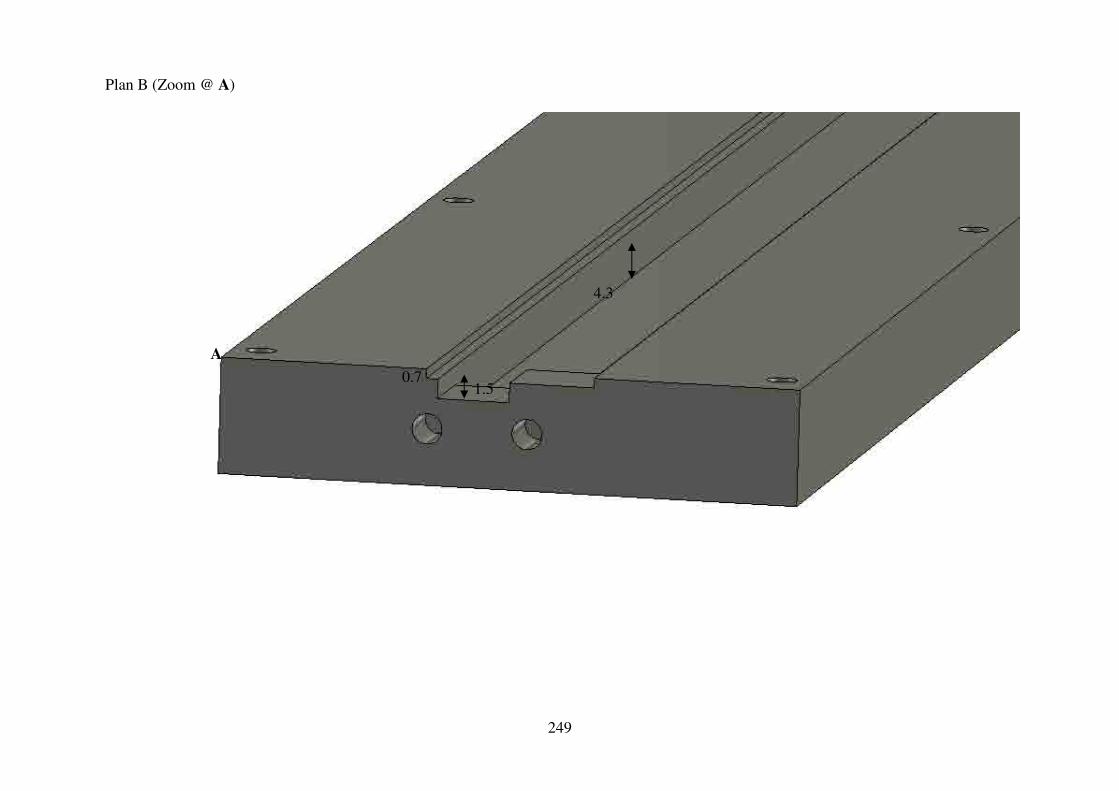
249
Plan B (Zoom @ A)
A
1.5 0.7
4.3

250
Plan B (Zoom @ A)
W1=17.75 W5=17.75 W4=7.3 W3=6.2
W2=1
W7=1
W6=12.5
h=8
A

251
Plan B (Zoom @ A)
L=6
D=2.6
V=5
10.65 2.5
D=2.6
17.935
26.575
8.64
5.18
0.7
1.5
10
A
A

252
Plan B (Zoom @ B)
B
4.3
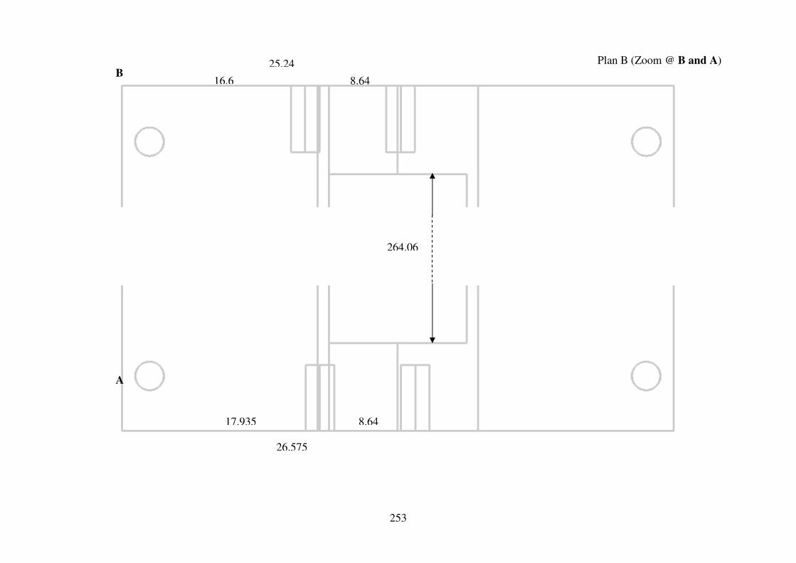
253
Plan B (Zoom @ B and A)
A
B
17.935
26.575
8.64
16.6
25.24
8.64
264.06

254