Modular ultrasound arrays with co-integrated electronics
17
Modular ultrasound arrays with co-integrated electronics Robert Wodnicki, USC University of Southern California Department of Biomedical Engineering Ultrasound Transducer Resource Center (UTRC)
Transcript of Modular ultrasound arrays with co-integrated electronics

Modular ultrasound arrays with
co-integrated electronics
Robert Wodnicki, USC
University of Southern California
Department of Biomedical Engineering
Ultrasound Transducer Resource Center (UTRC)
14th Int. Symp. on Nondestructive Characterization of Materials (NDCM 2015) - www.ndt.net/app.NDCM2015

Background/Mo-va-on
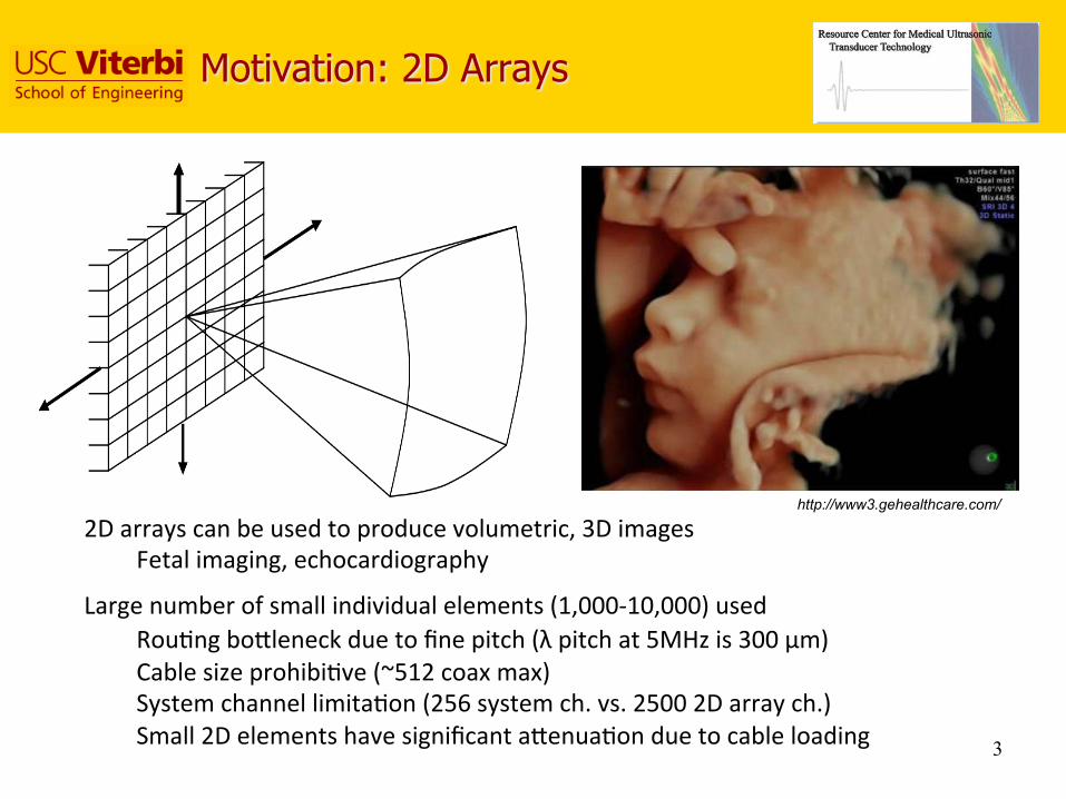
Motivation: 2D Arrays
3
2D arrays can be used to produce volumetric, 3D images
Fetal imaging, echocardiography
Large number of small individual elements (1,000‐10,000) used
Rou-ng boGleneck due to fine pitch (λ pitch at 5MHz is 300 μm)
Cable size prohibi-ve (~512 coax max)
System channel limita-on (256 system ch. vs. 2500 2D array ch.)
Small 2D elements have significant aGenua-on due to cable loading
http://www3.gehealthcare.com/

Solutions for 2D Arrays
4
Sparse arrays to reduce channel count (Holm, 1995)
Local electronics integrated at the probe
Sub Array Processors (SAPs) for local beamforming (Savord, 2003)
Switching matrix (Reconfigurable Arrays) to group elements (Erikson, 1996)
Improved sensi-vity for small elements
Reduced channel count (256 channels instead of 2500, or 10000 channels)
Savord et al, IUS, 2003 Thomenius et al, UFFC 2014

Modular 2D Arrays

Modular 2D Arrays
6
Large Area array: 100 x 100 elements, from 3cm x 3cm up to 20 cm x 20 cm
Transducer arrays integrated directly with Applica-on Specific ICs (ASICs)
Area coverage achieved by -ling mul-ple acous-c/ASIC modules with organic interposer
“cMUTs” used as transducer technology
Poten-al advantages
Improved sensi-vity for small elements (reduced loading, reduced crosstalk)
Reduced interconnect complexity (10,000 chs 256 chs)
Challenges
Very dense electronics needed (unit cell must match transducer array pitch)
High voltage CMOS required (100Vpp transmit voltage)

Trenched cMUT Transducers
7
Trenched capaci-ve Micromachined Ultrasound Transducer (MEMs fabrica-on)
Can be assembled using standard electronic packaging processes (flip‐chip)
Electrical impedance higher than PZT (sensi-vity issue)
Elements can have wide bandwidth (>90%)
“Trench/Frame” cMUTs used due to “Bulk” processing (equivalent to TSV)
“Trench” Signal Electrode
Suppor-ng
Frame
Suppor-ng
Frame
Substrate
Cavity
Metal
Via
Metal Assembly Pad
Membrane 150 nm
Zhuang, UFFC 2009
22 μm
250 μm 90 μm

2D Array Integration Methods
8
Direct integra-on is ideal but very challenging (Daf et al, 2004 )
Yield issues, Fab compliance, cap-ve fab needed
Flip‐chip integra-on is a good highly integrated alterna-ve (Wygant et al, 2008 )
Large array requires way to escape ASIC I/Os (e.g. TSVs)
Interposer (flex, ceramic, organic build‐up) also used (Wodnicki et al, 2014 )
Constraints: ASIC size, CTE mismatch, rou-ng
Flip‐Chip Direct Integra2on http://www-kyg.stanford.edu/ Lemmerhirt et al, UFFC 2012

Large Area 2D Array Prototype Implementa-on

Tiled Large Area Array Prototype
10
Interposers used to create assembly mockup for -leable module
Interposer allows seamless -ling by covering gaps due to ASIC I/O pads
Prototype module dimensions: 2.4 cm x 4 cm, with 8x14 -led array of cMUT chips
Total transducer channel count: 28,672
Double‐sided flip assembly was used
Smaller and modular chips have higher yield and can select Known Good Die
Wodnicki et al, NIMA-A 2011
Acoustic Gap

Interposer Assembly Process
11
Modular assembly was used with standard electronic packaging processes
Micro‐BGAs (70 μm, Eutec-c SnPb) aGached to cMUTs by solder‐jet process (PacTech)
Pitch for assembly: 185 μm for cMUT devices, 150 μm for dummy ASICs
Under Bump Metalliza-on (UBM) op-mized to achieve uniformity of solder volume
Final thicknesses were: Ti/Ni/Au (0.015 μm/0.3 μm/0.1 μm)
Substrate was dual‐sided organic laminate build‐up (EndicoG Interconnect)
Substrate rou-ng: 9 layers, ~25um lines/spaces
Co‐planarity: +/‐10 μm (λ/10) local, 150 μm global (due to CTE mismatch)
Interposer Substrate
185 um 185 um
Woychik et al, SMTA 2009 Woychik et al, SMTA 2009
BGA
Ball

Unit Electronics Cell Circuitry
12
HV Switch Matrix LV Switch + Pulser
Unit cell needs to match the size of the individual 2D transducer element
Low voltage switches 10‐20x smaller than HV switches (local pulser used)
0.8 μm 2 metal, 50V CMOS/DMOS process
Lower Ron beGer to mi-gate signal aGenua-on
Thomenius et al, UFFC 2014
Thomenius et al, UFFC 2014

Results

Effects of Tiling and Yield
14
Simula-ons were performed using Field II (Jensen, Med. Bio, 1996)
Annular array with 18mm aperture, 20 equal width rings
Element pitch was 185 μm for fc = 8MHz and the focus was set at 50mm
Observed beamwidth: 0.69mm (both in eleva-on and azimuth)
Average side lobe energy: ‐40dB (for one‐way simula-on with 300 μm gaps)
Side lobes came up slightly (‐35dB) with 93% element coverage (due to yield)
Thomenius et al, UFFC 2014
Side lobes
Missing
Elements Gaps
Rings

Acoustic Interposer Array Prototype
1.25D linear array, 3 x 192 ch. (32 x 192 cMUTs)
Dimensions: 6mm x 36mm
cMUT chip array (2 x 12) -led on front surface
Dummy ASIC chips on backside (acous-c load)
Sensi-vity decreased by shorted cMUT elements
Low Vbias and less ac-ve elements
Spa-al resolu-on comparable to produc-on GE PZT probe
Contrast resolu-on limited by poor sensi-vity
Fc = 7.59MHz
FBW = 61%
~50V Bias
Fluorinert FC‐84
15
16x16 element
cMUT chip
Wodnicki et al, NIMA-A 2011
cMUT Probe GE PZT Probe
Lin et al, UFFC 2013
Lin et al, UFFC 2013

Conclusions
Volumetric imaging requires large channel count 2D arrays
Results in rou-ng boGleneck and loss of sensi-vity
Closely integrated cMUTs and ASICs were used to reduce channel count
Interposer‐based modular, -led architecture was used to improve yield
Acous-c simula-ons predicted acceptable image performance with gaps
between transducer chips and missing elements
However, shor-ng of cMUT devices caused significant element loss resul-ng
in reduced acous-c sensi-vity and poor contrast resolu-on
Future work should address cMUT shor-ng directly in order to improve yield
16

Acknowledgements
17
This work was performed at GE Global Research in Schenectady, NY.
Key personnel at GE: K. Thomenius, R. Fisher, C. Woychik, S. Cogan
Collaboration: Stanford (Prof. Pierre Khuri-Yakub, E. Lin, X. Zhuang),
Pac-Tech USA, Endicott Interconnect, Fraunhofer IZM
The project described was supported by Grant number 1R01CA1152677
from the National Cancer Institute. Its contents are solely the responsibility
of the authors and do not necessarily represent the official views of the
National Cancer Institute or NIH.
Some of the technology described was derived from work originally
supported by Grant number R01 EB002485 from NIBIB. Contents of this
publication are solely the responsibility of the authors and do not necessarily
represent the official views of NIH.