Modeling Methodologies for Dynamic Recon gurable … · Modeling Methodologies for Dynamic Recon...
96
Modeling Methodologies for Dynamic Reconfigurable Systems BY FABIO CANCARE M.Sc. Computer Engineering, Politecnico di Milano, Milan, Italy, 2007 THESIS Submitted as partial fulfillment of the requirements for the degree of Master of Science in Computer Science in the Graduate College of the University of Illinois at Chicago, 2008 Chicago, Illinois
Transcript of Modeling Methodologies for Dynamic Recon gurable … · Modeling Methodologies for Dynamic Recon...
Modeling Methodologies for Dynamic Reconfigurable Systems
BY
FABIO CANCAREM.Sc. Computer Engineering, Politecnico di Milano, Milan, Italy, 2007
THESIS
Submitted as partial fulfillment of the requirementsfor the degree of Master of Science in Computer Science
in the Graduate College of theUniversity of Illinois at Chicago, 2008
Chicago, Illinois
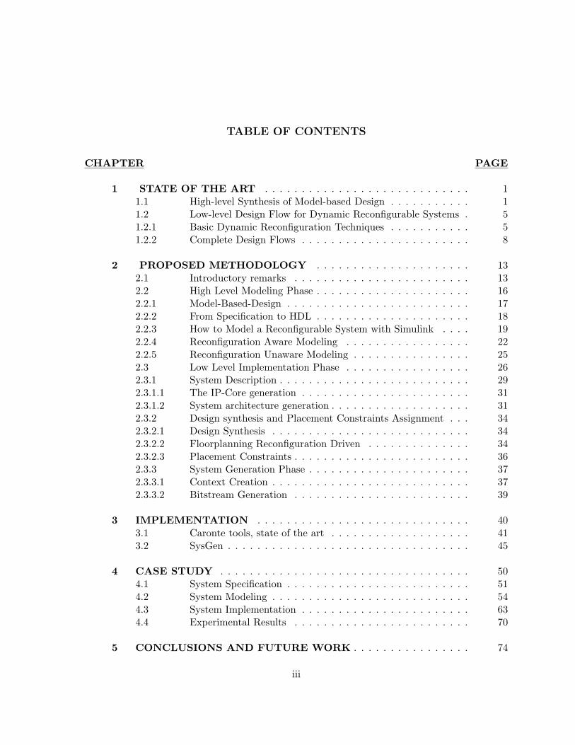
TABLE OF CONTENTS
CHAPTER PAGE
1 STATE OF THE ART . . . . . . . . . . . . . . . . . . . . . . . . . . . . 11.1 High-level Synthesis of Model-based Design . . . . . . . . . . . 11.2 Low-level Design Flow for Dynamic Reconfigurable Systems . 51.2.1 Basic Dynamic Reconfiguration Techniques . . . . . . . . . . . 51.2.2 Complete Design Flows . . . . . . . . . . . . . . . . . . . . . . . 8
2 PROPOSED METHODOLOGY . . . . . . . . . . . . . . . . . . . . . 132.1 Introductory remarks . . . . . . . . . . . . . . . . . . . . . . . . 132.2 High Level Modeling Phase . . . . . . . . . . . . . . . . . . . . . 162.2.1 Model-Based-Design . . . . . . . . . . . . . . . . . . . . . . . . . 172.2.2 From Specification to HDL . . . . . . . . . . . . . . . . . . . . . 182.2.3 How to Model a Reconfigurable System with Simulink . . . . 192.2.4 Reconfiguration Aware Modeling . . . . . . . . . . . . . . . . . 222.2.5 Reconfiguration Unaware Modeling . . . . . . . . . . . . . . . . 252.3 Low Level Implementation Phase . . . . . . . . . . . . . . . . . 262.3.1 System Description . . . . . . . . . . . . . . . . . . . . . . . . . . 292.3.1.1 The IP-Core generation . . . . . . . . . . . . . . . . . . . . . . . 312.3.1.2 System architecture generation . . . . . . . . . . . . . . . . . . . 312.3.2 Design synthesis and Placement Constraints Assignment . . . 342.3.2.1 Design Synthesis . . . . . . . . . . . . . . . . . . . . . . . . . . . 342.3.2.2 Floorplanning Reconfiguration Driven . . . . . . . . . . . . . . 342.3.2.3 Placement Constraints . . . . . . . . . . . . . . . . . . . . . . . . 362.3.3 System Generation Phase . . . . . . . . . . . . . . . . . . . . . . 372.3.3.1 Context Creation . . . . . . . . . . . . . . . . . . . . . . . . . . . 372.3.3.2 Bitstream Generation . . . . . . . . . . . . . . . . . . . . . . . . 39
3 IMPLEMENTATION . . . . . . . . . . . . . . . . . . . . . . . . . . . . . 403.1 Caronte tools, state of the art . . . . . . . . . . . . . . . . . . . 413.2 SysGen . . . . . . . . . . . . . . . . . . . . . . . . . . . . . . . . . 45
4 CASE STUDY . . . . . . . . . . . . . . . . . . . . . . . . . . . . . . . . . . 504.1 System Specification . . . . . . . . . . . . . . . . . . . . . . . . . 514.2 System Modeling . . . . . . . . . . . . . . . . . . . . . . . . . . . 544.3 System Implementation . . . . . . . . . . . . . . . . . . . . . . . 634.4 Experimental Results . . . . . . . . . . . . . . . . . . . . . . . . 70
5 CONCLUSIONS AND FUTURE WORK . . . . . . . . . . . . . . . . 74
iii
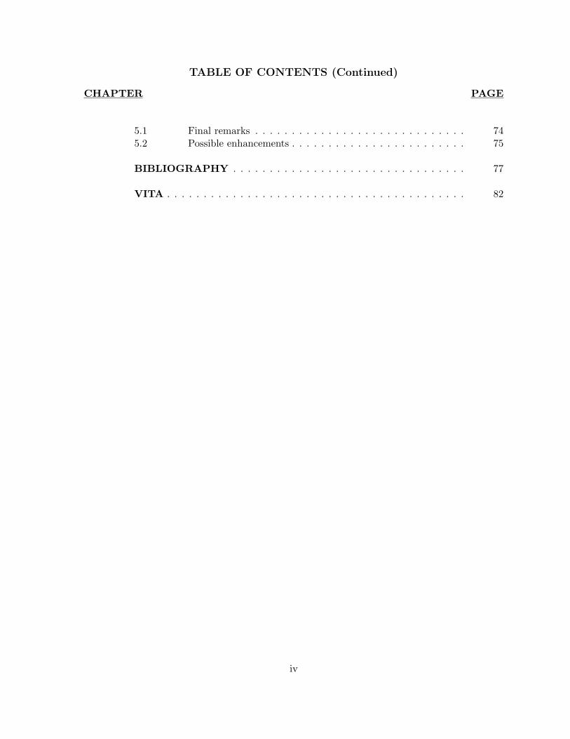
TABLE OF CONTENTS (Continued)
CHAPTER PAGE
5.1 Final remarks . . . . . . . . . . . . . . . . . . . . . . . . . . . . . 745.2 Possible enhancements . . . . . . . . . . . . . . . . . . . . . . . . 75
BIBLIOGRAPHY . . . . . . . . . . . . . . . . . . . . . . . . . . . . . . . . 77
VITA . . . . . . . . . . . . . . . . . . . . . . . . . . . . . . . . . . . . . . . . . 82
iv
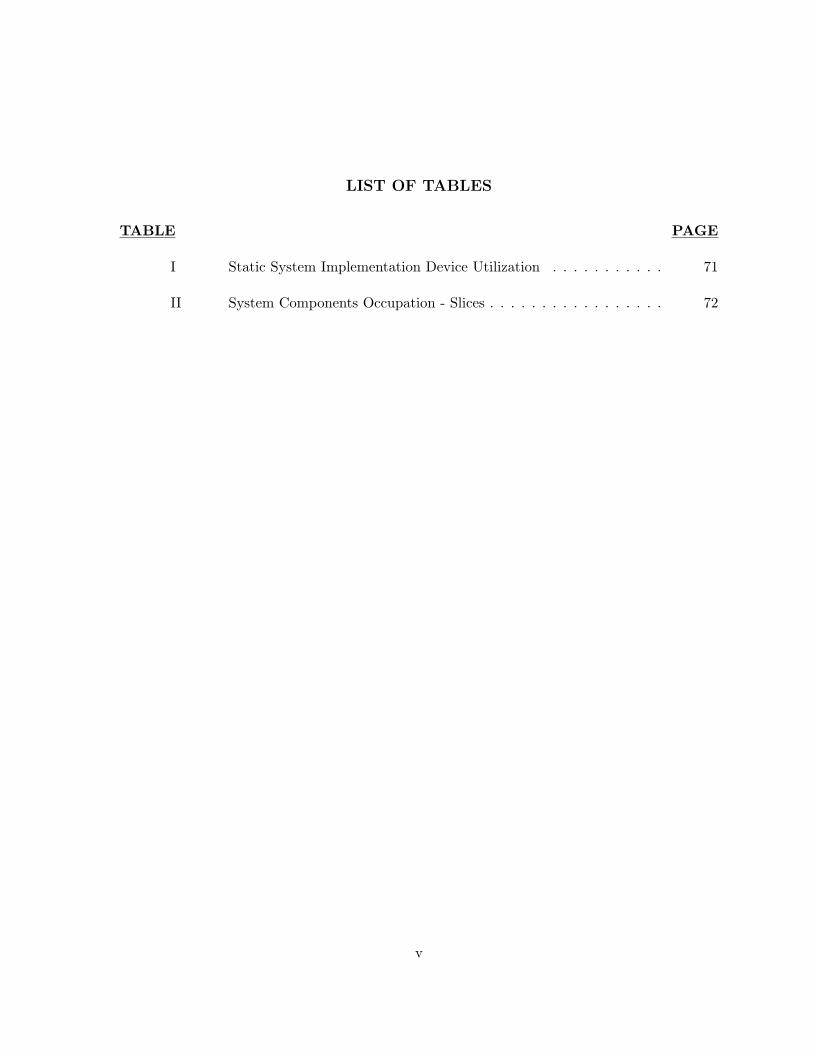
LIST OF TABLES
TABLE PAGE
I Static System Implementation Device Utilization . . . . . . . . . . . 71
II System Components Occupation - Slices . . . . . . . . . . . . . . . . . 72
v
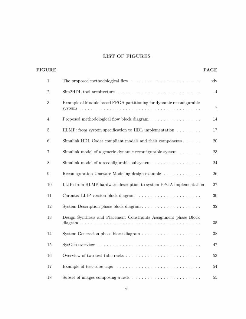
LIST OF FIGURES
FIGURE PAGE
1 The proposed methodological flow . . . . . . . . . . . . . . . . . . . . . . xiv
2 Sim2HDL tool architecture . . . . . . . . . . . . . . . . . . . . . . . . . . . 4
3 Example of Module based FPGA partitioning for dynamic reconfigurablesystems . . . . . . . . . . . . . . . . . . . . . . . . . . . . . . . . . . . . . . . 7
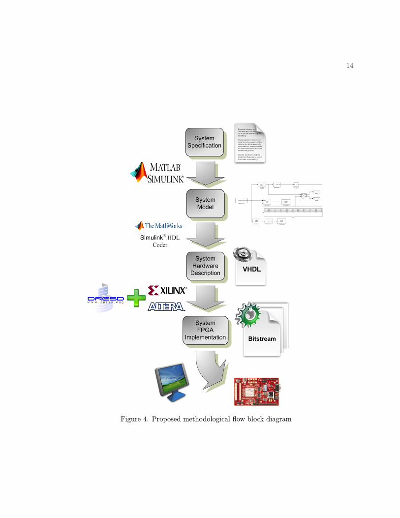
4 Proposed methodological flow block diagram . . . . . . . . . . . . . . . . 14
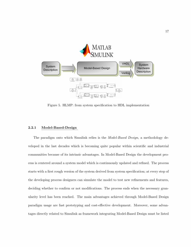
5 HLMP: from system specification to HDL implementation . . . . . . . . 17
6 Simulink HDL Coder compliant models and their components . . . . . . 20
7 Simulink model of a generic dynamic reconfigurable system . . . . . . . 23
8 Simulink model of a reconfigurable subsystem . . . . . . . . . . . . . . . 24
9 Reconfiguration Unaware Modeling design example . . . . . . . . . . . . 26
10 LLIP: from HLMP hardware description to system FPGA implementation 27
11 Caronte: LLIP version block diagram . . . . . . . . . . . . . . . . . . . . 30
12 System Description phase block diagram . . . . . . . . . . . . . . . . . . . 32
13 Design Synthesis and Placement Constraints Assignment phase Blockdiagram . . . . . . . . . . . . . . . . . . . . . . . . . . . . . . . . . . . . . . 35
14 System Generation phase block diagram . . . . . . . . . . . . . . . . . . . 38
15 SysGen overview . . . . . . . . . . . . . . . . . . . . . . . . . . . . . . . . . 47
16 Overview of two test-tube racks . . . . . . . . . . . . . . . . . . . . . . . . 53
17 Example of test-tube caps . . . . . . . . . . . . . . . . . . . . . . . . . . . 54
18 Subset of images composing a rack . . . . . . . . . . . . . . . . . . . . . . 55
vi
LIST OF FIGURES (Continued)
FIGURE PAGE
19 Canny Edge Detector . . . . . . . . . . . . . . . . . . . . . . . . . . . . . . 59
20 Edge Detection Test - Canny Method . . . . . . . . . . . . . . . . . . . . 60
21 Edge Detection Test - Sobel Method . . . . . . . . . . . . . . . . . . . . . 60
22 RGB to Grayscale Conversion implemented using Xilinx blocks . . . . . 62
23 RGB to Grayscale Test - Simulink vs Xilinx Solution . . . . . . . . . . . 62
24 Inpeco Simulink System Model . . . . . . . . . . . . . . . . . . . . . . . . 64
25 Inpeco Simulink System Model Compatible with HDL Coder . . . . . . 65
26 Static EDK System Architecture Block Diagram . . . . . . . . . . . . . . 69
vii
SUMMARY
It was 1960 when G. Estrin published a paper which actually gave birth to a new and promis-
ing scientific field, Reconfigurable Computing (1). However, despite the described “Fixed-Plus-
Variable” computer architecture was characterized by great potentialities, it received limited
researchers interest and Reconfigurable Computing remained an almost unexplored area until
the nineties. The main reason which can explain scientific community scarce consideration
toward this field for almost thirty years is the following: a computer architecture like “Fixed-
Plus-Variable (A fixed processor plus adaptable hardware) is much more complex than the
classical Von Neumann architecture; application development is, consequently, a much more
demanding task. Even if such systems offer remarkable computational power improvements, it
was possible to obtain comparable computational power improvements in different and more
promising ways firstly through silicon technology scaling and then through multi-core architec-
tures. Such a reason can also be inferred from a recent article written by G. Estrin himself (2).
Finally, in the last two decades, interest toward Reconfigurable Computing has grown when
scientists became aware that neither silicon technology nor multi-core solutions could continue
to improve processors computational power at the same rate as in past years; meanwhile al-
gorithms complexity constantly grew up and the classical possible alternative solution, ASICs
(Application-Specific Integrated Circuits), was always characterized by inflexibility.
The solution offered by Reconfigurable Computing is something that is placed between
hardware and software, “achieving potentially much higher performance than software, while
viii
SUMMARY (Continued)
maintaining a higher level of flexibility than hardware” (3). Research led to the development of
PLDs (Programmable Logic Devices) and, in particular, of FPGAs (Field Programmable Gate
Arrays). Such devices are different with respect to traditional ASICs because the implemented
functionalities can change during the devices lifetime. In particular, the implemented logic
function can change either when the device is inactive (Static Reconfiguration) or when it is
active (Dynamic Reconfiguration); the reconfiguration can involve the entire device area (Full
Reconfiguration) or a specific part (Partial Reconfiguration). Dynamic Partial Reconfiguration
(i.e. reconfiguration of a device portion while the remaining part is still functioning) is one of
the most interesting reconfiguration techniques; however, it is subject to the same limitation
reported before: applications development is a high demanding task. At the moment, at the
best of the author knowledge, there is no existing framework which can support designers in
completely implementing applications which exploit such technique.
Aim of this thesis work is to outline a new methodological flow that allows system designers
to make use of Dynamic Reconfiguration in a new and intuitive way. As a matter of fact,
Dynamic Reconfiguration can lead to enormous improvements in embedded systems design,
but it is, at the same time, characterized by complexity and toughness of use. The proposed
methodological flow is centered on the model-based design paradigm; it relies upon Simulink R©
by MathWorks (4) as long as several tools developed by the DRESD team (5) and by the
targeted FPGAs producers. Furthermore, a new tool, SysGen, is introduced to improve the
proposed flow automation.
ix
SUMMARY (Continued)
The main issue addressed by this thesis is the implementation of large designs onto FPGAs
with limited available resources. By applying the normal synthesis process to these systems
the outcome will be a failure due to the lack of resources. A flow based on Dynamic Partial
Reconfigurability will instead allow its successful implementation: since systems are composed
of blocks which need intermediate input(s) and produce intermediate output(s), these blocks can
be separately synthesized a priori and then hard-coded onto the PLD when their functionalities
become necessary. Intermediate input(s) can be provided either directly by blocks which are
still present onto the FPGAs or indirectly through internal or external memories.
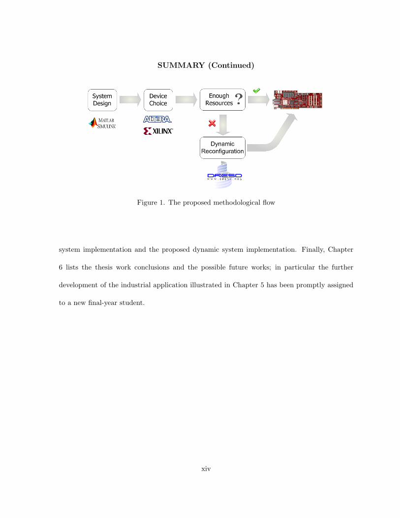
The methodological flow proposed in this thesis work is outlined in Figure 1. As reported
above, the obstacle overcame by Dynamic Partial Reconfigurability in the schema is the lack of
resources. It is important to point out that this is not the only advantage that can be achieved
through Dynamic Partial Reconfigurability: in scenarios where systems adaptability plays a
fundamental role the use of Dynamic Reconfigurability can lead to excellent performance and
low costs; even if it has not been scientifically proved yet, power consumption is lower since
without Dynamic Reconfigurability PLDs must be larger in order to host complete systems.
Finally, when system reliability is one of the most application critical aspects, Dynamic Partial
Reconfigurability can overcame local device failures by moving hardware modules placed on
damaged areas to different device areas (6).
The thesis work objectives described so far can be resumed in these key points:
• understand the high-level synthesis possibilities offered by the Simulink development en-
vironment;
x
SUMMARY (Continued)
• evaluate how to model dynamic reconfigurable system within Simulink;
• integrate the high-level dynamic reconfigurable system modeling process with the design
flow already developed by the DRESD Team;
• improve the DRESD Team design flow automation by designing a new tool, SysGen, able
to generate the netlists for full and partial bitstreams generation using different approaches
(7) (8);
• demonstrate the feasibility of the proposed approach implementing a complex application.
As previously described, the proposed flow relies upon the model based design paradigm (9);
the main motivation that leads to this choice is that systems complexity is growing and time-to-
market is becoming more stringent; therefore engineers, in order to meet these constraints, need
methodologies and tools which allow the fast development of complex architecture, giving the
possibility to reuse already developed components. The model-based design permits to build up
systems by modeling them incrementally, just as in top-down approaches. The process starts
with a generic model of the system which is continuously verified and improved until a final
model characterized by the necessary level of details is obtained. In the proposed methodological
flow systems are built using Simulink as graphical, intuitive front-end for model-based design.
Desired systems can be constituted by Simulink blocks which can be processed by the Simulink
HDL Coder and by any additional custom IP-cores written either in VHDL or in Verilog. It is
also possible to add others Simulink blocks which are non-compatible with Simulink HDL Coder
in order to verify system functionalities (e.g. Simulink signal generators); these blocks must be
removed or substituted before the high-level synthesis process. Also, FPGAs vendors provide
xi
SUMMARY (Continued)
their own sets of blocks, which exploit specific FPGA peculiarities (e.g. Xilinx supplies designers
with several filters which use DSP48 cells, present in different Xilinx FPGAs). Once the model is
completed and composed only of compatible blocks, the following FPGA implementation steps
are performed; designers feedbacks are required during few crucial phases of this semi-automatic
process.
The advantages of such an approach are noticeable: hardware engineers can build FPGA-
based systems which exploit Dynamic Partial reconfigurability using an environment, Simulink,
that is very common among DSP and algorithm engineers; such a common platform enhances
communication between different cooperating units and reduces the chance of interpretation and
translation errors. Furthermore, since Simulink provides a high-level system-modeling language,
system designers can rapidly produce a model that can be improved through simulation, co-
simulation and verification. Simulation and verification can be promptly performed within
Simulink, while co-simulation (i.e. a simulation that involves both Simulink blocks and external
blocks such as VHDL or Verilog cores) is achieved by using tools like ModelSim R© (10) by Mentor
Graphics. Further fine-grained improvements can be introduced by modifying the outputs of
the intermediate synthesis phases as it is usually done.
Dynamic Partial Reconfigurability is a research topic that involves an entire Politecnico
di Milano research group: the DRESD team. A lot of work has been done in the past few
years. However, a killer application has not been thought of yet; moreover, the majority of the
methodologies and tools developed have been widely tested through several case studies, but
xii
SUMMARY (Continued)
a real-world industrial application has not been produced yet. Therefore another objective of
this thesis work is to apply the proposed methodological flow to an industrial case study.
The novelties introduced by this thesis work can be summarized as follows:
• the study of a novel and complete methodology to implement Dynamic Reconfigurable
systems designed following the model-based paradigm;
• the improvement of Caronte, an already existing Low-Level Implementation Generation
flow developed at Politecnico di Milano;
• the full implementation of an industrial application exploiting the introduced methodol-
ogy.
The remainder of this thesis is organized as follows: Chapter 2 introduces the main related
works found in scientific literature; they can be split up into two categories, the first one
groups the papers concerning high-level synthesis using Matlab and Simulink as development
environment. The latter collects papers about dynamic reconfigurable systems design flows.
Chapter 3 describes the proposed methodological flow; it embeds both an high-level modeling
part relying on Simulink and a low-level implementation part based upon Caronte, a design flow
developed by the DRESD Team. Chapter 4 concerns the design of a new DRESD tool, SysGen,
created in order to increase the design flow automation level hence allowing to create dynamic
reconfigurable systems more rapidly. Chapter 5 shows how the proposed methodological flow has
been applied to the design of an industrial application. The Chapter describes both the modeling
phase and the implementation phase, pointing out the differences between a classical static
xiii
SUMMARY (Continued)
Figure 1. The proposed methodological flow
system implementation and the proposed dynamic system implementation. Finally, Chapter
6 lists the thesis work conclusions and the possible future works; in particular the further
development of the industrial application illustrated in Chapter 5 has been promptly assigned
to a new final-year student.
xiv
CHAPTER 1
STATE OF THE ART
Aim of this Chapter is to present the literature related to the proposed methodological flow,
highlighting advantages and disadvantages and pointing out unsolved issues. The proposed
flow, as seen in Chapter , is composed of a high-level modeling part and a low-level dynamic
system implementation part; therefore this Chapter is structured into two different parts as
well: Section 1.1 describes works related to high-level synthesis using Matlab R©/Simulink R© as
development environment while Section 1.2 is devoted to the analysis of already existing low
level flows for reconfigurable dynamic systems implementation.
1.1 High-level Synthesis of Model-based Design
As designs become larger and more complicated, it becomes necessary to first describe
them at a high level of abstraction; model-based design represent a possible solution, since it
allows to model systems using a high-level yet thorough language (11). Simulink (4) offers a
graphical development environment relying on the model-based design paradigm where systems
can be modeled through blocks performing basilar functions linked together to form a composite
architecture. Simulink is already a widespread environment for embedded systems verification,
since it permits to model them rapidly; it would become a still more powerful environment
by providing high-level synthesis support (i.e. the passage between a high-level language to a
hardware description language). Engineers and scientists became aware of the possibility to
1
2
improve Simulink with such support several years ago and it is possible to find several works
about this topic in literature.
The first one, at the best of the author knowledge, is a tool developed by A. Krukowsky
and I. Kale (12) in 1999. The work consists in analyzing the Simulink text representation of
a model (i.e. the .mdl files produced by Simulink containing every information about system
blocks and links) and finding similarities with VHDL constructs. Since the two representations
are quite similar, the authors developed a tool which produces VHDL files holding data about
module interfaces (i.e. Simulink block signals) and module connections (i.e. Simulink links).
Obviously the tool does not provide VHDL or Verilog modules implementation; the authors
proposed as solution to this drawback the creation of a database holding Simulink blocks HDL
representation. Moreover, the tool works only if signals within the Simulink model are forced
to be unsigned integer signals.
In addition to A. Krukowsky and I. Kale, also I. Grout was one of the first scientists which
faced the problem being analyzed; in (13) he proposed a semi-automatic approach to convert
Simulink design into VHDL files; he identified one of the main issues that must be overcome,
the conversion from float values to signed/unsigned values, and he implemented a conversion
utility to deal with it. However, its proposed approach concerns a very small set of Simulink
blocks (Control System blocks such as inport, outport, gain and unit delay) and it continuously
requires user interaction.
(14) is not a directly related work, but it is important since it contributed to the creation of
the Embedded Matlab Language (15). In fact the authors described a system which is able to
3
parse Matlab files composed of a very limited set of instructions and produce optimized VHDL.
Embedded Matlab Language is, in fact, a subset of the Matlab language which can be efficiently
translated into HDL exploiting a mechanism quite similar to the one proposed in this paper.
(16) is an improved version of the compiler described in (14); several features have been added,
one of them is the possibility to generate HDL modules exploiting specific device peculiarities.
It must be pointed out that, however, the last two papers described something that in the end
was not developed. The authors idea, in fact, was to describe hardware cores using Matlab
code and then convert them to HDL code; however, this approach was overwhelmed by other
similar approaches which perform translation from C/C++ code to HDL code.
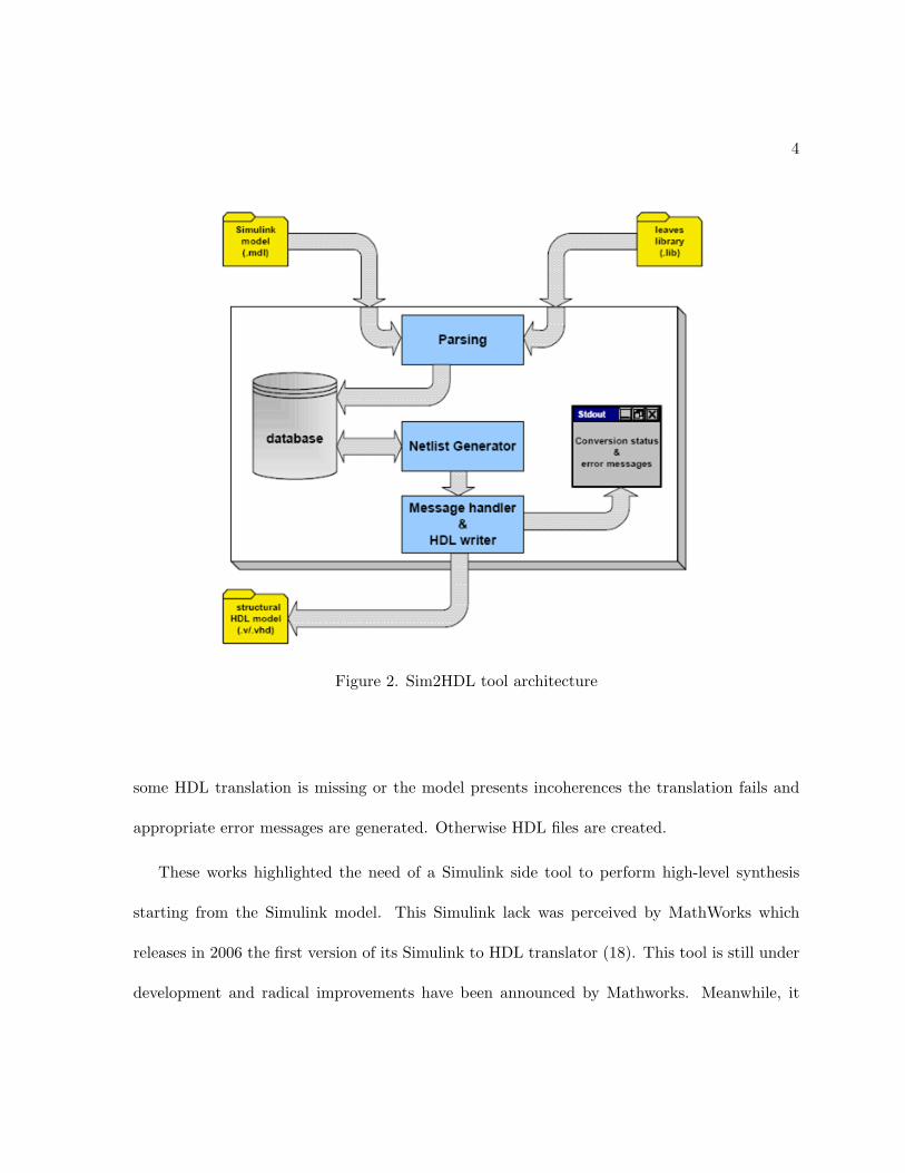
(17) is a very interesting paper about a tool performing conversion from Simulink model
to HDL files, Sim2HDL. A tool overview is shown in Figure 2. The Sim2HDL architecture
is interesting because it was taken into account my MathWorks engineer while developing the
Simulink HDL Coder; the system processes two different kinds of input: the first type of input
is the Simulink model itself (a text file describing the model developed within Simulink) while
the second one is a set of predefined Simulink blocks translation in HDL. Simulink HDL Coder R©
has a similar structure: it processes .mdl files and it produces .v or .vhd files exploiting internal
libraries (e.g. HDLlib) which contain blocks HDL code. Then Sim2HDL has a parsing stage
which eliminates useless information from the model file and stores relevant data into a database
along with HDL translation of used blocks. A final generator tool tries to produce HDL file by
substituting Simulink block with available HDL translations. This stage is in charge of managing
connections between blocks and reporting them into opportune HDL module wrappers. If
4
Figure 2. Sim2HDL tool architecture
some HDL translation is missing or the model presents incoherences the translation fails and
appropriate error messages are generated. Otherwise HDL files are created.
These works highlighted the need of a Simulink side tool to perform high-level synthesis
starting from the Simulink model. This Simulink lack was perceived by MathWorks which
releases in 2006 the first version of its Simulink to HDL translator (18). This tool is still under
development and radical improvements have been announced by Mathworks. Meanwhile, it
5
is possible to use it to create interesting designs as J. Mosterman, a MathWorks researcher,
showed in (19).
1.2 Low-level Design Flow for Dynamic Reconfigurable Systems
Dynamic Reconfigurable systems can be implemented either developing an ad-hoc solution
or following a generalized design flow. In the first case designers must employ a considerable
amount of time in creating the ad-hoc system architecture; the ad-hoc solution developed can
be characterized by higher performance than the one which can be obtained following general
design flows, however the chances of errors and malfunctionings are, at the same time, higher.
The latter solution is based upon well-defined general methodologies, which can be applied
to almost any design. It must be pointed out that complex low-level design flows relies on
technique developed by FPGA producers which are described in Section 1.2.1. Complete state
of the art design flows are instead depicted in Section 1.2.2.
1.2.1 Basic Dynamic Reconfiguration Techniques
The first fundamental document describing how to introduce Dynamic Partial Reconfigu-
ration in FPGA applications is (7); it states that there are two main styles of dynamic partial
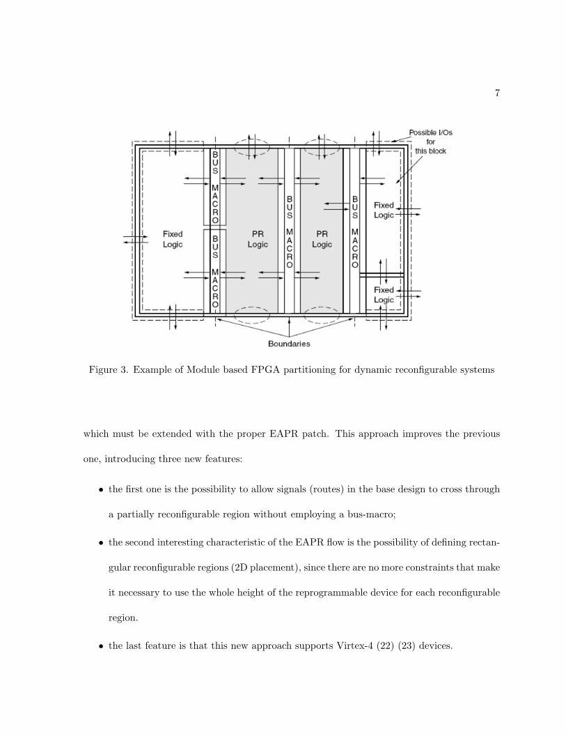
reconfiguration: Module-based and Difference-based.
• Module-based reconfiguration style relies upon the Modular-based design paradigm
(20) and it is characterized by the subdivision of the PLD devices in several areas, called
either fixed or reconfigurable slot. Hardware components placed in fixed slots can not
be reconfigured at run-time; instead, Hardware components placed in reconfigurable slots
can be altered and substituted while the device is working. It must be highlighted that
6
the remaining part of the device continues to work during the reconfiguration process. An
important aspect of Module-based style is related to the communication infrastructure.
Using this technique the communication between adjacent fixed modules resembles to
communication lines in normal FPGA systems, while communication between reconfig-
urable slots or between a fixed slot and a reconfigurable slot needs particular expedients.
In this cases intermodule communication is possible using particular macro hardware
called bus macro; these macros provide a fixed communication infrastructure which can-
not be changed during reconfiguration processes. An example of FPGA partitioning and
bus macro instantiation is shown in Figure 3. It must be pointed out that Modular-based
style imposes several architectural constraints: besides bus macro, slot vertical dimension
must be equal to device height, slot horizontal dimension must follow a specific pattern
and, above all, the FPGA must be a Virtex, a Virtex II or a Virtex II-Pro.
• Difference-based reconfiguration style is a simpler method with respect to Module-
based since it does not require neither FPGA partitioning nor bus macro; however it
is suitable only when the reconfiguration process concerns a very small design part. A
difference bitstream is created by analyzing the two design versions and it can be used to
alter FPGA functionalities.
Recently, a novel design flow based on the module-based approach just described has been
introduced: the Early Access Partial Reconfiguration (8) (EAPR). It is a Xilinx design
flow developed exclusively for some versions of Integrated Synthesis Environment (21) (ISE),
7
Figure 3. Example of Module based FPGA partitioning for dynamic reconfigurable systems
which must be extended with the proper EAPR patch. This approach improves the previous
one, introducing three new features:
• the first one is the possibility to allow signals (routes) in the base design to cross through
a partially reconfigurable region without employing a bus-macro;
• the second interesting characteristic of the EAPR flow is the possibility of defining rectan-
gular reconfigurable regions (2D placement), since there are no more constraints that make
it necessary to use the whole height of the reprogrammable device for each reconfigurable
region.
• the last feature is that this new approach supports Virtex-4 (22) (23) devices.
8
In such a scenario it can be noticed how this new flow provides a deep improvement in the design
of reconfigurable architecture but without changing the context in which also the previous one
was working.
1.2.2 Complete Design Flows
The just exposed basic flows define how it is possible to use FPGAs as a support for dynamic
reconfigurable systems; however, adapting these methodologies step by step performing the
necessary operations is a time-consuming and error-prone process. An alternative solution is to
follow design flows which rely upon techniques described in 1.2.1 but which automatize most
phases allowing to reach the same result with less efforts.
The Caronte flow (24) (25) can be placed among the complete design flows for dynamic
reconfigurable system implementation. The Caronte flow has been completely developed at
Politecnico di Milano and it is based on the classic module-based approach, hence supporting
Virtex, Virtex II and Virtex II-Pro. The flow can be decomposed into three main phases:
• The first phase is called HW-SSP Phase (Hardware Static System Photo Phase); goal of
this phase is to compute the set of states which the FPGA will assume at run-time. Each
state is different from the others and corresponds to a specific FPGA configuration; it is
made up by two different parts: a static part containing every system hardware component
and a reconfigurable part containing a certain number of reconfigurable hardware cores.
By consequence each state can be considered as a photo taken at system run-time. The
only input of this phase is a partitioned system specification.
9
• In the second phase, the Design Phase, all the information needed to compute the re-
configuration bitstreams are collected. These bitstreams will be later used to physically
implement the embedded reconfiguration of the FPGA. Aim of this phase is to identify
the structure of each reconfigurable block and to solve all the placement and communica-
tion problems. Placement problems are related to the choice of the FPGA reconfigurable
area that will be used to implement the reconfigurable hardware components while com-
munication problems are related to bus macro instantiation.
• The last phase is the Bitstream Creation Phase. The output of this phase consists
of a set of bitstreams that will be ready to be loaded on the FPGA and will be able to
configure the reprogrammable device with the corresponding state, defined in the previous
phases. These bitstream will be either complete (i.e. holding information to configure the
whole FPGA) or partial (i.e. holding information to reconfigure a specific FPGA portion.
The Caronte flow is still under development and the DRESD Team is working to enhance it.
A more recent version of the just described original Caronte flow is exposed in (26) and it will
described thoroughly in Chapter 3. Furthermore, also this thesis work contributes to extend
the Caronte flow by introducing a new tool, SysGen, which allows to make Caronte more
flexible with respect to basic flows and available development tools; the tool will be described
in Chapter 4.
Besides the Caronte flow, other works deal with the creation of complete design flows for
dynamic reconfigurable systems which are based on the Xilinx module-based (7) technique.
One of this work is the Proteus project (27); it basically consists in a design flow tailored for
10
a specific FPGA architecture intended to be PC-based. The FPGA is embedded into a board
which exchanges data with a standard processor using the PCI interface. Besides the FPGA, the
developed board contains a flash memory storing the base configuration bitstream. The FPGA
base configuration places onto the FPGA fixed components that are used to manage the PCI
interface and the ICAP (Internal Configuration Access Port); moreover several bus macros are
instantiated to link the static part containing the control logic to the reconfigurable part. The
reconfigurable part at system startup does not hold any hardware component but, at run-time,
it can be configured with different and exchangeable hardware cores. The Proteus framework
(27), however, does not provide substantial improvements in the definition of a novel design flow
for partial reconfigurable architecture. This framework can be useful to develop applications
that will find benefits in the execution over the proposed reconfigurable platform, in fact Proteus
will take care of the communication between the host PC and the reconfigurable architecture
and it will manage the download of the necessary partial reconfiguration bitstreams. Anyway, it
presents all the drawbacks already presented in the Xilinx standard module-based design flow.
Another interesting flow is the one proposed in (28). The PaDReH framework aims at de-
signing dynamically and partially reconfigurable systems based on single FPGAs. The flow is
composed of three phases: Design Capture and Functional Validation, Partitioning and Schedul-
ing, Physical Synthesis and Reconfiguration Infrastructure. Even if all these three phases are
mentioned only the last one has been implemented. The main contribution of this work can
be found in the definition of a hardware core used to manage the reconfiguration since the
bitstream generation phase is basically the same proposed by Xilinx in (7).
11
The work described in (29) is a useful information source for those who want to deeply
understand how Xilinx module-based reconfiguration style operates. However, it cannot be
defined as a novel approach for dynamic system design since it does not introduce any innovation
with respect to the classical module-based dynamic partial reconfiguration flow.
In (30) two different techniques for implementing modular partial reconfiguration using
Xilinx Virtex FPGAs are proposed and compared. The first method has been already intro-
duced and widely commented, it is the design flow, proposed by Lim and Peattie in the Xilinx
application notes, (7). The second technique, proposed by the authors in (30), has removed
the mono-dimensional constraints and it can be considered as the ancestor of the EAPR (8)
approach. This method, called Merge Dynamic Reconfiguration, is based on a bitstream
merging process and reserved routing. Due to the reserved routing, it is possible to have stati-
cally routed signal to pass through a reconfigurable area since the static and the reconfigurable
modules are placed and routed independently it is possible to reserve already used routing re-
sources from the static core to prevent the reconfigurable module to use the same resources. In
this context the separation between the design of the static component and the reconfigurable
ones is clearly stated but the drawback is the reduction in the freedom of the router. Once
that a partial reconfiguration bitstream has to be downloaded on the FPGA, the Merge Dy-
namic Reconfiguration approach does not write it directly to the reconfiguration memory but
it reads back the current configuration from the device and it updates it with the data from the
partial bitstream in a frame-by-frame manner, minimizing the amount of memory requested to
store the bitstream. The result of this method is the possibility to have two or more modules

12
overlapping their vertical placement constraints, allowing modules to be shaped and positioned
arbitrarily but is has the drawback of dramatically incrementing the reconfiguration time.
CHAPTER 2
PROPOSED METHODOLOGY
This Chapter describes, step by step, the various phases composing the proposed method-
ology. Starting from the project specification, the flow drives designers through every imple-
mentation stage, ending with the final bitstreams. Such an approach constitutes a novelty in
Reconfigurable Computing field; up to now, no complete frameworks and methodologies were
developed, at the best of the author knowledge, for implementing applications which exploit
Dynamic Reconfiguration.
2.1 Introductory remarks
The proposed methodology relies on Simulink R© as high-level development framework for
reconfigurable systems and on an enhanced version of the Caronte flow (24) (25) as low-level
implementation generator. Figure 4 shows a block diagram of the main flow phases; each one
of them will be explained in detail within this Chapter.
Since the first Simulink version, MathWorks includes among the available side tools Real-
Time Workshop R© (RTW) (31); basically, RTW is able to generate ANSI/ISO C-compliant
code for applications developed either through Simulink models or Embedded MatlabTM
code
(a subset of the Matlab language which can be compiled into efficient code for embedded
implementation). In September 2006, on the basis of RTW success among algorithm engineers
(RTW raises abstraction level by allowing to realize complex C algorithms using an high-
13
14
Figure 4. Proposed methodological flow block diagram
15
level modeling language such as Simulink), MathWorks released the first version of Simulink
HDL Coder (18); this tool can generate synthesizable VHDL or Verilog code starting from
Simulink models or Embedded Matlab code, extending Matlab and Simulink capabilities to
design embedded systems. The idea behind this thesis work is that Simulink and Simulink
HDL Coder can be used not only to realize traditional embedded systems, but also to realize
Dynamic Reconfigurable embedded systems. In order to achieve such a result, two possible
modeling approaches within Simulink were devised and must be followed by designers. The
first one is addressed to users who do not have any knowledge about Dynamic Reconfiguration
or who do not want to take care of Dynamic Reconfiguration; applications are modeled in
the traditional Simulink way and Dynamic Reconfiguration is automatically introduced in the
following design flow phases. The latter is addressed to users who want to directly manage
Dynamic Reconfiguration; in this case models must be specified using well-defined Simulink
patterns developed in this thesis work.
For what concerns low-level system implementation, the Caronte flow has been enhanced
on the Hardware (HW) and Reconfigurable Hardware (RHW) side, revisiting the System Gen-
eration phase and introducing a new tool which deals with it: SysGen. Essentially, SysGen
is able to create final bitstreams (i.e. files which hold either complete FPGA configurations
or configurations related to device specific portions) following different approaches. In its first
version, the tool can handle two different methodologies to support Partial Reconfiguration:
Module-based Partial Reconfiguration, defined in (7) and Early Access Partial Reconfiguration
(EAPR), described in (8). However, the tool is organized in order to support further future
16
approaches. Besides System Generation Phase, the others two phases, System Description and
Design Synthesis and Placement Constraints Assignment are implemented exploiting several
tools which have been developed by members of the DRESD team. As final remark it must be
outlined that the remaining Caronte side, the Software (SW) one, was almost not taken into
account in this thesis work for sake of simplicity; the process of partially reconfiguring FP-
GAs is driven by an external entity such as a workstation (External Partial Reconfiguration).
If processor(s) support is needed, there exist proprietary Simulink blocks which model both
hard-cores (e.g. PowerPC 405) and soft-cores (e.g. Microblaze).
The following Sections describe in a more detailed way the proposed methodology. Section
2.2 is about the modeling phase conducted within Simulink environment. From now one it will
be referred as High Level Modeling Phase. Section 2.3 is about the enhanced version of Caronte
used to obtain a dynamic reconfigurable system implementation. This second phase is called
Low Level Implementation Phase.
2.2 High Level Modeling Phase
It can be possible to identify two different main phases composing the proposed methodol-
ogy. The High Level Modeling Phase is the first one and it concerns the passage from system
specification to a first, raw, system hardware description (Figure 5). As previously said, the
framework used to obtain such a description is Simulink R©, a MathWorks software which can
be employed to model, simulate and analyze dynamic systems. Before analyzing in detail this
phase, it is important to highlight the motivation behind the choice of Simulink as development
framework for reconfigurable systems.
17
Figure 5. HLMP: from system specification to HDL implementation
2.2.1 Model-Based-Design
The paradigm onto which Simulink relies is the Model-Based Design, a methodology de-
veloped in the last decades which is becoming quite popular within scientific and industrial
communities because of its intrinsic advantages. In Model-Based Design the development pro-
cess is centered around a system model which is continuously updated and refined. The process
starts with a first rough version of the system derived from system specification; at every step of
the developing process designers can simulate the model to test new refinements and features,
deciding whether to confirm or not modifications. The process ends when the necessary gran-
ularity level has been reached. The main advantages achieved through Model-Based Design
paradigm usage are fast prototyping and cost-effective development. Moreover, some advan-
tages directly related to Simulink as framework integrating Model-Based Design must be listed
18
in addiction to paradigm ones: since Simulink can constitute a common design environment
across project members chances of interpretation and translation errors are almost reset to
zero. Also, Simulink automatically generates the C code which implements the system avoiding
hand-coding errors. Finally, it must be outlined that it comes with several standard blocks li-
braries along with many on-line block repositories, so applications can be designed using already
existing blocks and rarely users need to create blocks from scratch.
2.2.2 From Specification to HDL
Besides just described advantages, the main reason that justifies Simulink usage within the
methodology proposed in this thesis work is the introduction, in September 2006, of an Hard-
ware Description Generator called Simulink HDL Coder. MathWorks decided to add this side
tool to Simulink suite after the success of another similar side tool: Real-Time Workshop. RTW
is able to generate C implementation of Matlab R© and Simulink algorithms and models; this
turned out to be a great advantage for those designers who need an effective implementation
of their already simulated and validated systems. Similarly, Simulink HDL Coder is able to
generate HDL (either using VHDL or Verilog) implementation of Matlab and Simulink algo-
rithms and models, allowing to verify designs directly on FPGAs and ASICs. Before Simulink
HDL Coder, Simulink was already widely used by embedded system engineers to create and
test embedded system models; with an automatic HDL generator it is believed that Simulink
will become an even more relevant software for embedded system design, which explains the
interest for this tool in the thesis work.
19
2.2.3 How to Model a Reconfigurable System with Simulink
It must be pointed out that both Simulink and Simulink HDL Coder are not thought
up for dynamic reconfigurable embedded systems; however, since systems exploiting Dynamic
Reconfiguration are obviously dynamic systems, it is possible to create their models within
Simulink and then to obtain their hardware description thanks to Simulink HDL Coder. As
anticipated before, this thesis work develops two possible approaches for modeling dynamic
reconfigurable systems:
• Reconfiguration Aware Modeling is meant for users who want to directly manage Dynamic
Reconfiguration. A good knowledge of Reconfigurable Computing techniques constitutes
a basilar prerequisite.
• Reconfiguration Unaware Modeling is almost just as traditional modeling. Systems are
defined following the classical Simulink methodology and Reconfiguration is automatically
introduced later, with the goal of reducing PLDs resources usage.
Before describing in a more detailed way these two approaches it is worthwhile to say
a few words about something they have in common: the process of creating Simulink HDL
Coder compliant models. In fact Simulink HDL Coder can not generate, by now, an hardware
description of every possible Simulink model; such a result constitutes Simulink HDL Coder
mission (MathWorks) but it is still far away to be achieved. Currently designers who want to
develop Simulink HDL Coder compliant models can build them using three different sets of
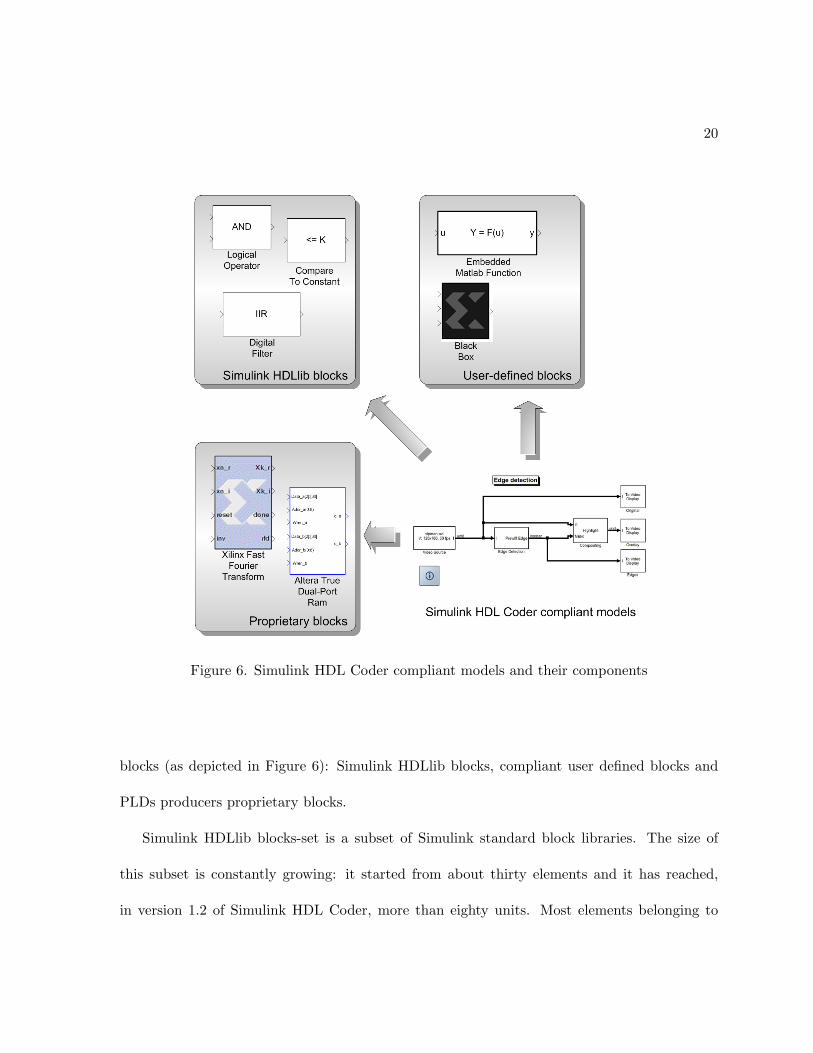
20
Figure 6. Simulink HDL Coder compliant models and their components
blocks (as depicted in Figure 6): Simulink HDLlib blocks, compliant user defined blocks and
PLDs producers proprietary blocks.
Simulink HDLlib blocks-set is a subset of Simulink standard block libraries. The size of
this subset is constantly growing: it started from about thirty elements and it has reached,
in version 1.2 of Simulink HDL Coder, more than eighty units. Most elements belonging to
21
HDLlib blocks-set are basic components such as input ports and logic operators; however there
are exceptions like digital filters and other signal processing blocks. Compliant user defined
blocks can be either Embedded Matlab functions or HDL custom cores. In the first case
users develop algorithms using a subset of the Matlab language: Embedded Matlab language
(EML) (15); Simulink HDL Coder will then convert EML code into HDL code. In the latter
case users can create Simulink blocks by specifying cores signal interfaces along with their
HDL implementations (VHDL or Verilog files). The drawback is that models can still be
validated within Simulink but simulation must be performed using third-party tools; in order
to simplify this process, Mathworks introduced a tool which interfaces Simulink to ModelSim R©
(A simulation environment for ASIC and FPGA designs, (10)): Link for ModelSim R© (32).
Finally, proprietary blocks are those belonging to libraries developed by PLDs vendors. In fact,
after Simulink HDL Coder entry, producers like Xilinx Inc. and Altera corp. developed specific
Simulink blocks compatible with HDL generator along with the necessary design flows which
produce bitstreams from Simulink models. Device characteristics and system constraints are
specified within Simulink models and are the only inputs, besides correct models, needed by
these tools to synthesize system designs. The tools developed by Xilinx Inc. and Altera Corp.
are respectively System Generator for DSP (33) and DSP builder (34).
Compliant blocks are linked together to form complete systems using conventions listed
in (4). Lastly, an important feature offered by Simulink is the possibility to model systems
in a hierarchical way. The concept of sub-system as a single Simulink block which can be
expanded plays a fundamental role in both the developed techniques which are described in the
22
following subsections. Reconfiguration Aware Modeling is the first technique outlined during
this thesis work; it is meant for creating dynamic reconfigurable system models. The other
technique, Reconfigurable Unaware Modeling, is completely different because it is meant for
creating system models which can then be implemented exploiting Dynamic Reconfiguration.
2.2.4 Reconfiguration Aware Modeling
As it can be inferred, in Reconfiguration Aware Modeling Dynamic Reconfiguration must be
explicitly introduced by users in system models; therefore a necessary user prerequisite is a good
knowledge of Dynamic Reconfiguration mechanisms. Systems must be designed highlighting
which parts are static and which parts are reconfigurable. Figure 7 shows a Simulink model of
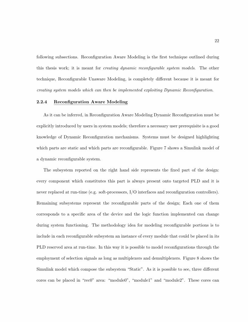
a dynamic reconfigurable system.
The subsystem reported on the right hand side represents the fixed part of the design:
every component which constitutes this part is always present onto targeted PLD and it is
never replaced at run-time (e.g. soft-processors, I/O interfaces and reconfiguration controllers).
Remaining subsystems represent the reconfigurable parts of the design; Each one of them
corresponds to a specific area of the device and the logic function implemented can change
during system functioning. The methodology idea for modeling reconfigurable portions is to
include in each reconfigurable subsystem an instance of every module that could be placed in its
PLD reserved area at run-time. In this way it is possible to model reconfigurations through the
employment of selection signals as long as multiplexers and demultiplexers. Figure 8 shows the
Simulink model which compose the subsystem “Static”. As it is possible to see, three different
cores can be placed in “rec0” area: “module0”, “module1” and “module2”. These cores can
23
Figure 7. Simulink model of a generic dynamic reconfigurable system
provide completely different functionalities as long as represent the same functionality improved
or adapted to external changes. Cores are activated and deactivated using a selection signal
“sel”; they receive a generic input signal called “DataIn” and produce a generic output signal
called “DataOut”. Despite Figure 8 shows stark module interfaces, it is possible to specialize
and enrich interfaces as needed; however, it is fundamental that cores placed in the same
reconfigurable area must be characterized by the same interface. A remark regarding the block
called “Reconfiguration cost”: it has been included to model a delay in signal propagation
caused by the time employed to reconfigure an area with a new module. Such block can
24
be placed in different parts of the model and it can be useful to explore possible dynamic
reconfiguration drawbacks. In this particular case it has been used to model output change
delay when the input is constant.
The use of subsystems during this phase as long as naming conventions are basilar for
subsequent low level implementation phases. In fact Simulink HDL Coder organizes VHDL and
Verilog files using as tree structure the one delineated by system hierarchies. Such organization
will constitute a fundamental step in automating the whole methodological flow.
Figure 8. Simulink model of a reconfigurable subsystem
25
2.2.5 Reconfiguration Unaware Modeling
Reconfiguration Unaware Modeling is a technique for creating system models which can then
be implemented exploiting Dynamic Reconfiguration. Differently from Reconfiguration Aware
Modeling, Simulink designs do not contain any detail regarding Dynamic Reconfiguration. Users
develop their applications following simple design rules and then reconfiguration is automatically
introduced in subsequent design phases. At a first glance this second technique seems much
better than the previous one because it considerably simplifies the design process; however it
must be outlined that it is not optimal and it can be greatly outperformed by Reconfiguration
Aware Modeling, as it will explained after its description.
In Reconfiguration Unaware Modeling system models must adhere to a specific pattern:
they must be composed of an ordered succession of blocks. These blocks will be placed onto
FPGAs either one by one or in small groups; placing blocks one by one means that the number of
resources required by the system is very low: in fact at run-time, at every instance of time there
will be only one of the possible blocks implemented onto the FPGA, hence resources required
are those used by more demanding cores. This solution is advantageous in term of resources
usage but system performance is very low due to continuous reconfigurations. Placing group of
blocks can partially solve performance issues; this approach however requires third-party tools
support. It is in fact necessary to chose a specific FPGAs among those supported by either
Xilinx DSP System Generator or Altera DSP builder and then to make use of resource evaluator
blocks. In this way it will be possible to size cores in order to comply with FPGA resource
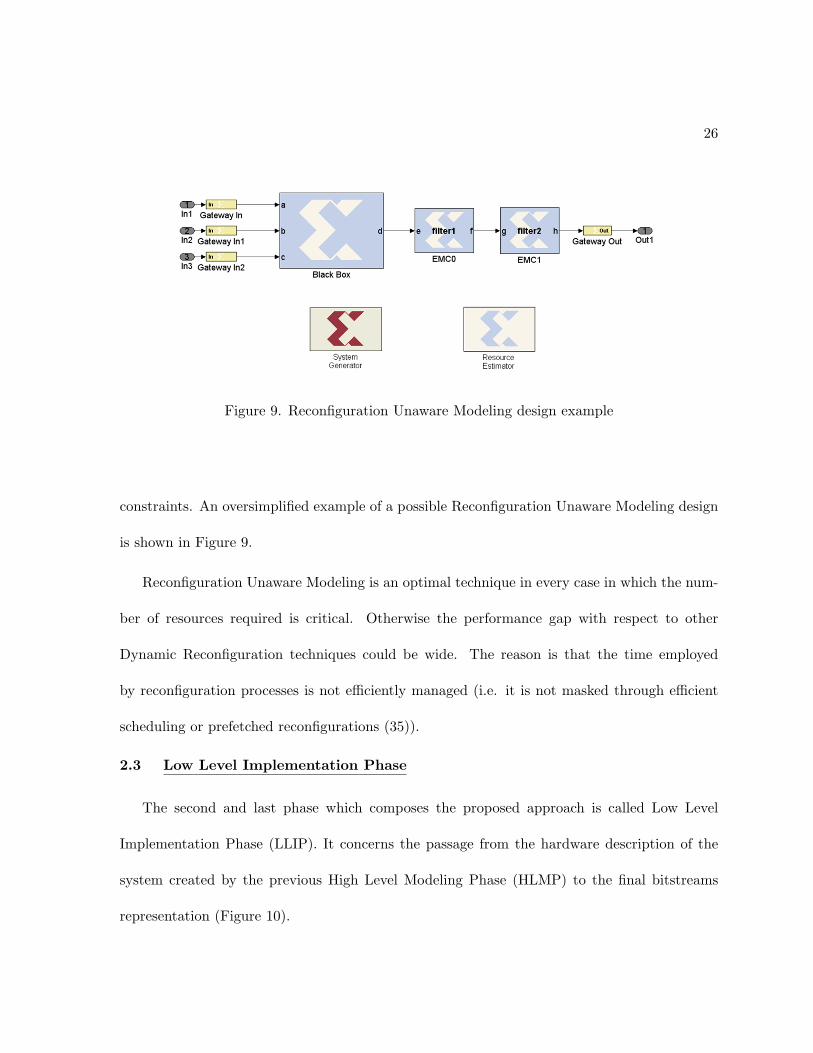
26
Figure 9. Reconfiguration Unaware Modeling design example
constraints. An oversimplified example of a possible Reconfiguration Unaware Modeling design
is shown in Figure 9.
Reconfiguration Unaware Modeling is an optimal technique in every case in which the num-
ber of resources required is critical. Otherwise the performance gap with respect to other
Dynamic Reconfiguration techniques could be wide. The reason is that the time employed
by reconfiguration processes is not efficiently managed (i.e. it is not masked through efficient
scheduling or prefetched reconfigurations (35)).
2.3 Low Level Implementation Phase
The second and last phase which composes the proposed approach is called Low Level
Implementation Phase (LLIP). It concerns the passage from the hardware description of the
system created by the previous High Level Modeling Phase (HLMP) to the final bitstreams
representation (Figure 10).
27
Figure 10. LLIP: from HLMP hardware description to system FPGA implementation
This phase is based on an enhanced version of the classical Caronte flow ((25) and (24)
describe the original version); the phase goal is to generate the low-level implementation of the
desired system in order to make it possible to physically configure the target device to realize
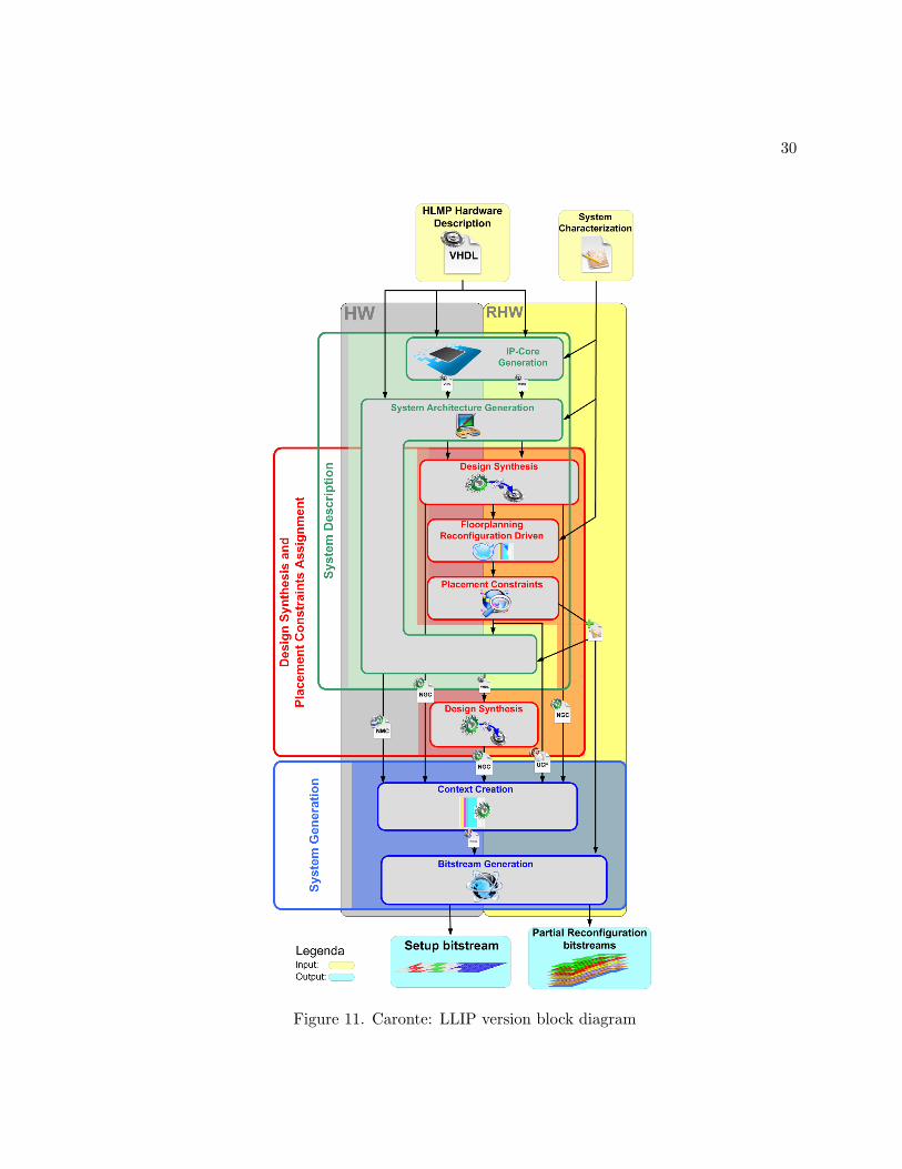
the original specification. A diagram showing the whole process is presented in Figure 11. As
it is possible to see, the flow is split up into two parts, hardware (HW) side and reconfigurable
hardware (RHW) side; moreover, it is composed of three phases: System Description phase,
Design Synthesis and Placement Constraints Assignment phase and System Generation phase.
The input that must be provided to LLIP is constituted by the hardware description of
the various system components generated by the HLMP phase along with information such
as targeted device and time constraints. The first operation carried out by System Descrip-
tion phase is the extension of HDL cores with a communication infrastructure that makes it
28
possible to interface them with a bus-based communication channel (IP-core generation). Af-
ter this initial step, the static components of the system are used to realize the design of the
static architecture, while the reconfigurable components are handled in a different way, as re-
configurable IP-Cores; in other words they will be kept separated from the static part of the
architecture until the beginning of the System Generation phase, while the static components
will be synthesized together with the static part of the architecture. In order to implement
the correct communication infrastructure between the static component and the reconfigurable
ones, the component placement constraints need to be known. Therefore, before the generation
of the HDL description of the overall architecture the placement constraints phase needs to
be executed. It was decided to consider the System Description and the Design Synthesis and
Placement Constraints assignment phases as separated even if, as shown in Figure 11, they
are extremely connected one another. As it is possible to see, the System Description phase is
needed to generate the HDL architectural solution while the Design Synthesis and Placement
Constraints assignment phase find its rationale in the identification and in the corresponding
assignment of the physical placement constraints needed to define the overall structure of the
final architectural solution. Once these partially concurrent phases are concluded, the netlist
and hard-macro generated files describing both the static part and the reconfigurable parts are
passed as input to the System Generation phase along with a constraints file. After a merging
step (Context Creation), the final step is the Bitstreams Generation which is necessary to obtain
the bitstreams that will be used to configure and to partially reconfigure the reprogrammable
device.
29
With respect to the previous implementation of Caronte, the low-level flow employed by
the proposed methodology is implemented in a different way for what concerns the System
Generation phase. Previously, instead of a comprehensive tool, there were single scripts working
with well-defined tool versions and system design constraints. SysGen replaces these scripts by
providing a unique front-end that automatically derives which particular procedure(s) can be
used to implement Partial Reconfiguration. The remaining part of this Section is devoted to a
detailed description of the steps mentioned in this introduction.
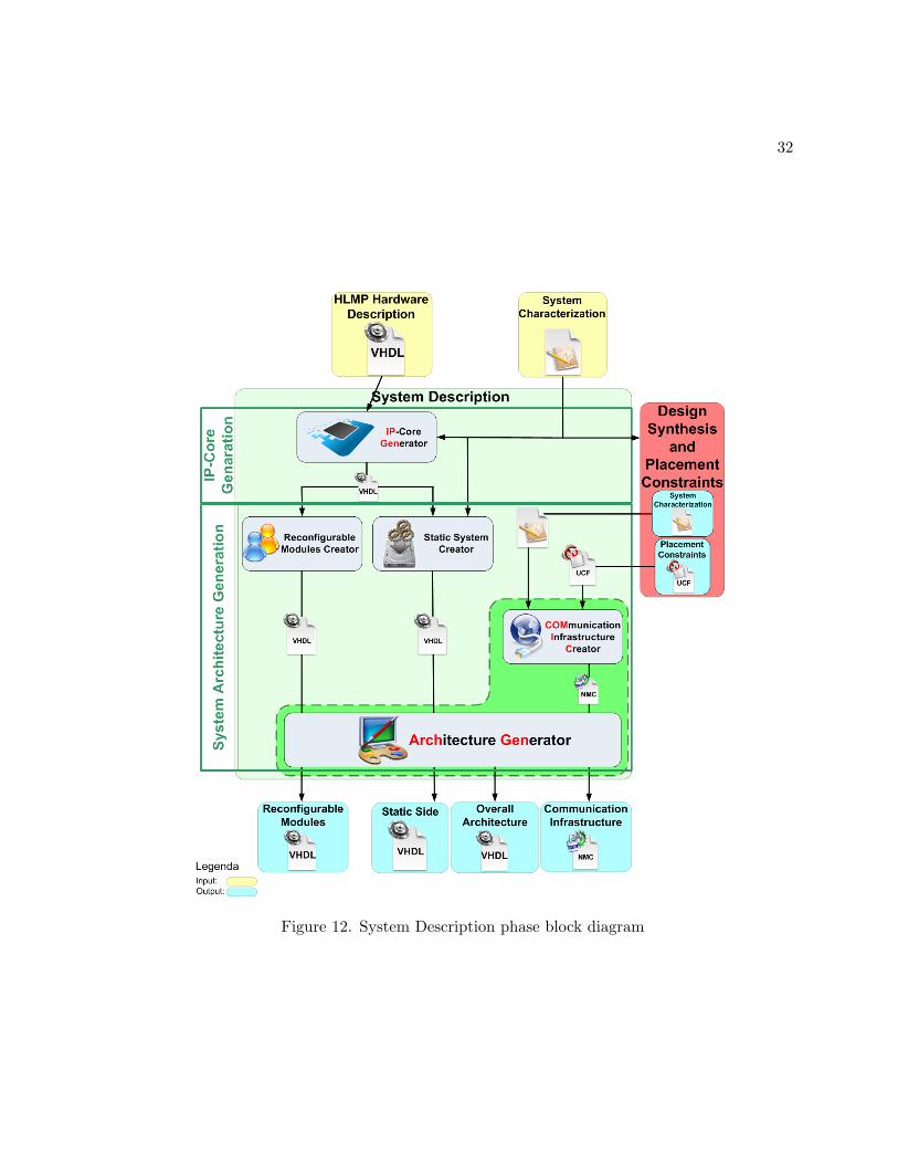
2.3.1 System Description
The first phase of the flow, as shown in Figure 12, consists in the creation of all the nec-
essary files used to describe the reconfigurable solution (i.e. the VHDL descriptions of each
reconfigurable component, the VHDL description of the overall architecture and the macro
HW used to define the communication infrastructure). This phase accepts as input the HDL
descriptions of the components which implement the desired application and some information
regarding the overall solution. It is possible to identify four different set of files used to describe
the corresponding four basic architecture components: the reconfigurable side, the static side,
the communication infrastructure and the overall system architecture. The system description
phase has been organized into two different subsequent steps: the IP-Core generation and the
system architecture generation, described below. The former is the most application oriented
phase. At this point all the functionalities that have to be implemented in HW, both static and
reconfigurable, are defined. The system architecture phase is used to define the overall system
architecture. This architecture is composed of a set of application-independent components,
30
Figure 11. Caronte: LLIP version block diagram
31
such as the reconfigurator core1 and the GPP, and a set of components that belong to the
application that has to be implemented.
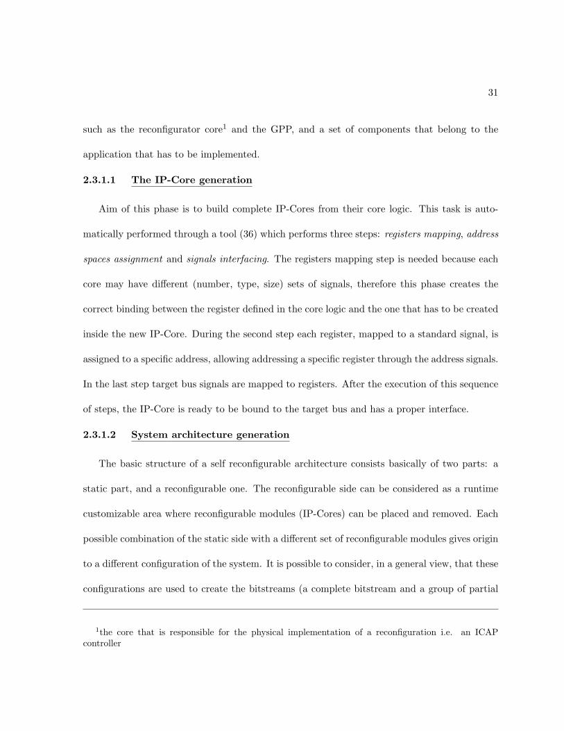
2.3.1.1 The IP-Core generation
Aim of this phase is to build complete IP-Cores from their core logic. This task is auto-
matically performed through a tool (36) which performs three steps: registers mapping, address
spaces assignment and signals interfacing. The registers mapping step is needed because each
core may have different (number, type, size) sets of signals, therefore this phase creates the
correct binding between the register defined in the core logic and the one that has to be created
inside the new IP-Core. During the second step each register, mapped to a standard signal, is
assigned to a specific address, allowing addressing a specific register through the address signals.
In the last step target bus signals are mapped to registers. After the execution of this sequence
of steps, the IP-Core is ready to be bound to the target bus and has a proper interface.
2.3.1.2 System architecture generation
The basic structure of a self reconfigurable architecture consists basically of two parts: a
static part, and a reconfigurable one. The reconfigurable side can be considered as a runtime
customizable area where reconfigurable modules (IP-Cores) can be placed and removed. Each
possible combination of the static side with a different set of reconfigurable modules gives origin
to a different configuration of the system. It is possible to consider, in a general view, that these
configurations are used to create the bitstreams (a complete bitstream and a group of partial
1the core that is responsible for the physical implementation of a reconfiguration i.e. an ICAPcontroller
32
Figure 12. System Description phase block diagram
33
reconfiguration bitstreams) that will be used to set-up the system (the complete bitstream) and
to swap from one configuration to another (the partial bitstreams).
The reconfigurable modules creation accepts as input the modules generated by IPGen
and provides as output the VHDL description of the corresponding reconfigurable modules.
The static system creation stage takes as input, in addition to the base architecture used to
define the core of the static side of the self reconfigurable architecture, the IP-Cores, provided
by IPGen, that have been selected to be inserted in the static part of the architecture. The
static system creator adds to the base architecture all the IP-Cores that have to be considered
as static components aiming at defining the VHDL description of the static component of the
desired architecture.
As shown in Figure 11 the next two stages of the System architecture generation phase,
even if included in this phase, come after the Design synthesis and Placement Constraints
Assignment phase, because they require placement information on the layout of the overall
architecture.
COMIC, COMmunication Infrastructure Creator, is a tool that has been developed to im-
plement the communication infrastructure creation stage. It takes as input the placement
constraints identified by the design synthesis and placement constraints assignment phase and
the the information regarding the communication protocol that has to be implemented and it
provides as output the corresponding macro-hardware which is used to implement the commu-
nication infrastructure. Finally, the architecture generation stage consists in the creation of
the VHDL description of the top architecture where the static component, the communication
34
infrastructure and the necessary reconfigurable components are instantiated. This is achieved
by analyzing the VHDL descriptions generated by the previous stages.
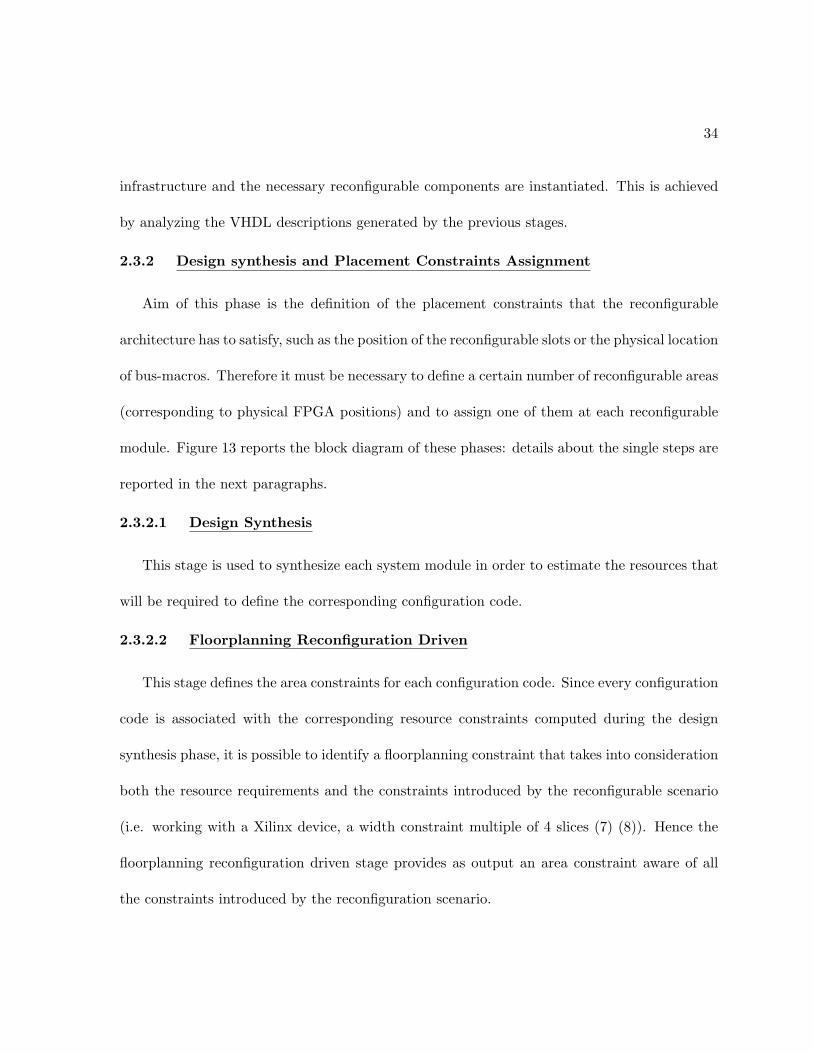
2.3.2 Design synthesis and Placement Constraints Assignment
Aim of this phase is the definition of the placement constraints that the reconfigurable
architecture has to satisfy, such as the position of the reconfigurable slots or the physical location
of bus-macros. Therefore it must be necessary to define a certain number of reconfigurable areas
(corresponding to physical FPGA positions) and to assign one of them at each reconfigurable
module. Figure 13 reports the block diagram of these phases: details about the single steps are
reported in the next paragraphs.
2.3.2.1 Design Synthesis
This stage is used to synthesize each system module in order to estimate the resources that
will be required to define the corresponding configuration code.
2.3.2.2 Floorplanning Reconfiguration Driven
This stage defines the area constraints for each configuration code. Since every configuration
code is associated with the corresponding resource constraints computed during the design
synthesis phase, it is possible to identify a floorplanning constraint that takes into consideration
both the resource requirements and the constraints introduced by the reconfigurable scenario
(i.e. working with a Xilinx device, a width constraint multiple of 4 slices (7) (8)). Hence the
floorplanning reconfiguration driven stage provides as output an area constraint aware of all
the constraints introduced by the reconfiguration scenario.
35
Figure 13. Design Synthesis and Placement Constraints Assignment phase Block diagram
36
2.3.2.3 Placement Constraints
Aim of this stage is the identification of the placement constraints that will be used to
implement each configuration code. The floorplanning reconfiguration driven stage provides a
set of feasible area constraints, but the problem that still needs to be solved is the identifica-
tion of the placement constraints taking into consideration the fact that those configuration
codes are not configured as single cores on the reconfigurable device, but they have to share
the reconfigurable resources with other configuration codes. The UCF Builder and Analyzer
(BUBA) tool takes as input the starting area solutions computed by the previous stage, a static
scheduling of the application and the information regarding the reconfigurable device that has
to be used to implement the desired design. All this information is provided in the system
characterization file. Due to these parameters BUBA assigns, using a greedy algorithm, the
placement constraints to each module trying to minimize the number of reconfigurations (37).
This is possible due to the fact that a module can be executed at different times and not only
once. In such a scenario there might be a placement solution able to keep configured a configu-
ration code on the reconfigurable device, without affecting the quality of the schedule, without
having to reconfigure the same module twice or more just because it is no longer available on
the reconfigurable device. Once the new placement constraints are defined this information is
stored into the system characterization file and into the UCF file and provided respectively to
the system architecture generation stage in the System Description phase to implement the cor-
rect communication infrastructure and to the context creation stage in the System Generation
phase.
37
2.3.3 System Generation Phase
The previous two phases produce all the necessary files (i.e., HDL descriptions, UCF file,
macro-hardware definitions, etc. etc.) to describe the desired system, both in its static and
reconfigurable side. The last phase of the flow is the System Generation phase, see Figure 14.
The System Generation phase, can be used to support both the Xilinx Early Access Partial
Reconfiguration-based, (8), and the Module-based, (7), reconfigurable architecture design flow.
This phase has been divided in two different stages: the Context Creation and the Bitstream
Generation.
2.3.3.1 Context Creation
This phase has been organized into three different stages: Static Side Implementation,
Reconfigurable Modules Implementation and Context Merging. The former one accepts as input
the HDL files1 generated during the system description phase and the placement information
defined via the design synthesis and placement constraints assignment phase. Aim of this
stage is the physical implementation of the static side of the final architecture. The placement
information of this component will be provided as input to the Context Merging phase of
the final architecture. A second output, working with the EAPR flow, is represented by the
information of the static side components that are placed in the reconfigurable modules region
i.e., routing, CLBs usage. This information is stored in the arcs exclude file, and it is represented
by the dot line, in Figure 14, used to bind the Static Side Implementation and the Reconfigurable
1NMC and NGC files
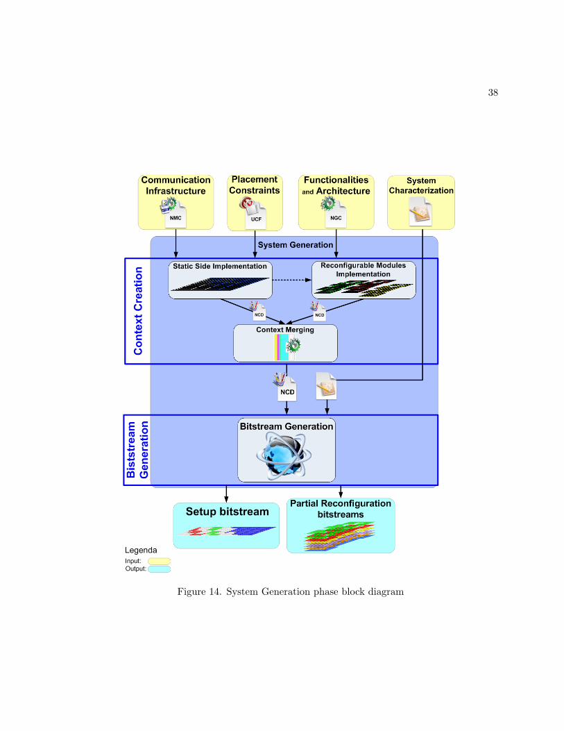
38
Figure 14. System Generation phase block diagram
39
Modules Implementation stages. The Reconfigurable Modules Implementation stage needs as
input the placement information for each module and the corresponding VHDL files defined
during the previous two phases and the arcs exclude file. This stage defines the physical
implementation of each reconfigurable component that has to be passed as input to the hardware
merging phase. It is composed of three different steps: the NGDBuild, the mapping and the
final place and route stage. The Reconfigurable Modules Implementation stage needs to be
executed with each reconfigurable component. Finally, the Context Merging stage produces as
result the merging of the outputs produced by the two previous stages.
2.3.3.2 Bitstream Generation
The Bitstream Generation stage consists in the generation of both a complete bitstream,
based on the top that configures the system and a set of empty modules. Then for each module
two partial bitstreams have to be created: one is used to configure it over an empty module
and another one to restore the empty configuration. In such a situation it is not necessary, at
compile time, to compute and to know all the possible reconfiguration combinations between
all the modules. The bitstreams created during this stage allow to fully implement the system
onto the targeted PLD.
CHAPTER 3
IMPLEMENTATION
This chapter is devoted to the description of a new tool designed to improve the Caronte
(24) (25) design flow automation. Caronte, as pointed out in the previous Chapter, is a design
flow for dynamic reconfigurable systems developed at the Politecnico di Milano by the DRESD
Team. In the last few years this flow has been firstly conceived and then successfully used for
implementing several applications on different programmable logic devices (PLDs); however,
the implementation of these applications required a lot of effort and one of the main problems
was the lack of tools able to support the engineer during the different design flow phases.
Hence it was decided to start creating a correspondence between the design flow phases and
some practical tools able to support the designer during the system implementation.
One of the thesis goals is to continue this automation process by introducing a new tool,
SysGen, which must deal with the Caronte System Generation Phase. In particular the objective
is realizing a tool able to provide at the same time the support for several partial reconfiguration
paradigms (7) (8) and the support for different versions of FPGA vendors tools (38) (21). The
design of this new DRESD tool is described in Section 3.2; Section 3.1, instead, describes the
results achieved so far concerning the Caronte support tools.
40
41
3.1 Caronte tools, state of the art
Partial Dynamic Reconfiguration can lead to enormous improvements in embedded systems
design, but it is, at the same time, characterized by complexity and difficulty of application due
to a lack of supporting tools. The DRESD Team introduced the Caronte design flow to allow
designing dynamic reconfigurable systems following a well-defined and systematic methodology;
moreover, to simplify this process, several support tools were created. This Section aims at
describing the actual Caronte support implementation progress, defining the tools generated so
far along with the flow phases interested by these tools.
The first tool taken into consideration in this brief Caronte implementation state of the
art is IPGen (36). IPGen is an IP-Core generator which receives as input the VHDL code
of an hardware component and produces as output an IP-Core ready to be inserted into an
Embedded Development Kit (EDK) (38) system. Thus IPGen is able to make the hardware
component compatible with the On-chip Peripheral Bus (OPB) (39) by analyzing the core I/O
signals and creating a core stub which binds these signals to the standard OPB signals. The
final IP-Core interface generated by IPGen and linked to this core stub is the standard Xilinx
OPB IPIF (On-chip Peripheral Bus IP-core InteFace). IPGen automates a stage of the Caronte
System Description phase: the IP-core Generation stage.
The second tool encountered when analyzing the Caronte flow from the beginning to the
end is ArchGen. Generally speaking, ArchGen is able to separate the fixed part of the system
from the reconfigurable part of the system. Once the EDK system is ready (i.e. the process of
adding the application-specific IP-Cores to the EDK base architecture is finished) it is possible
42
to obtain a static implementation of the system by running the synthesis process; in order
to generate such an implementation, EDK creates also some VHDL files and, in particular, a
VHDL file called system.vhd which represents the whole system as a composition of hardware
components linked one to each other. This file can be processed by ArchGen which generates,
given a reconfigurable hardware components list, the fix.vhd file, holding information about
the system fixed part, and the top.vhd file, representing the entire system in which there is
an instance of the fixed part and an instance of the reconfigurable part. ArchGen automates a
stage portion of the Caronte System Description phase: a portion of the System Architecture
Generation stage.
The third tool described is BUBA, the UCF Builder and Analyzer. This tool has been
introduced with the goal of automating the production of the system constraint file (UCF file).
This file is produced, in its first version, by EDK itself (EDK adds constraints about signals
to FPGA pin correspondence); then it must be edited in order to add constraints about area
boundaries. This last modification is partially automated by BUBA, which analyzes the various
reconfigurable system components and proposes a possible FPGA partitioning. BUBA deals
with a stage of the Caronte Design synthesis and Placement Constraints Assignment phase:
the Placement Constraints stage.
The fourth tool taken into account in this brief review is COMIC, the COMmunication
Infrastructure Creator. The COMIC task is to allow communication between the fixed part of
the system and the reconfigurable one. As previously described, it is necessary to add some
hard macros to the system architecture in order to create communication channels between
43
the fixed part and the reconfigurable part and, also, between different reconfigurable slots.
The bus macros must be placed exactly on parts boundaries, hence it is necessary to add
specific placement constraints related to these bus macros. COMIC is able to generate the
needed macros (NMC files) according to the chosen communication protocol and their placement
constraints (statements to be added to the UCF file) according to the already specified area
constraints. COMIC automates a stage portion of the Caronte System Description phase: a
portion of the System Architecture Generation stage.
The last tools (but it is more correct to call them flows) concern the Caronte System Gen-
eration phase and, in particular, the Context Creation stage. There exist two different flows:
the first one is called Acheronte and applies Partial Reconfiguration using the Module-based
methodology described in (7). The second one is called INCA and applies Partial Reconfigu-
ration using the Early Access Partial Reconfiguration methodology defined in (8).
Acheronte was developed by the DRESD Team in 2006 and it is fully described in (40).
Briefly, it is a flow which allows the generation of both full and partial bitstreams for the imple-
mentation of dynamically reconfigurable systems following the rules defined in (7). Acheronte
receives as input by the previous phases of the Caronte flow the following items:
• the netlist files (NGC files) related to both the fixed architecture and the reconfigurable
modules;
• the hard macro files (NCD files) describing the bus macro used to realize the communi-
cation infrastructure;
• the number of reconfigurable areas instantiated within the FPGA;
44
• the constraint files (UCF files) containing the FPGA area constraints and the bus macro
placement constraints;
• the reconfigurable modules schedule information (i.e. when a reconfigurable module is
needed).
It produces as output netlist files (NCD files) that are then converted into bitstreams. It
is important to point out that the Acheronte flow works only with specific area constraints
(e.g. the vertical dimension of the FPGA areas must correspond to the device height) and with
specific development tools versions (i.e. it works only with ISE 7.1i).
INCA was developed by the DRESD Team in 2007 and it is fully described in (41). Differ-
ently from Acheronte, INCA is based on the Early Access Partial Reconfiguration methodology
(8). Similarly to Acheronte, however, it requires as input the netlist files describing both the
fix part and the reconfigurable parts, the hard macro files concerning the bus macros and the
constraint file listing the area and placing constraints. Other side information are not needed
because INCA relies on a well-defined folder tree. Each file must be placed in the correct folder
in order to make INCA works. The main tree folder contains:
• the base folder holding the netlist files of the fixed architecture;
• the HDL folder containing the HDL files of the fixed part and of the reconfigurable
modules;
• the recmod folder which in turn includes one folder for each reconfigurable module netlist;
45
• the top folder holding the netlist file of the overall architecture (the fixed part plus the
reconfigurable parts).
INCA as well has some limitations: for example it is compatible only with version 8.2i of
ISE (21) patched with the Partial Reconfiguration patch.
Both Acheronte and INCA are implemented as batch files and each one of them has a
different user interface. It is desirable to have one single tool able to deal with the Caronte
Context Creation stage, characterized by an unique interface and by the possibility of interacting
with different tools versions and making use of different Partial Reconfiguration methodologies.
Such a tool represents one of the thesis goals and its design is described in a detailed way in
Section 3.2.
3.2 SysGen
This section deals with the description of a new DRESD tool aimed at automating the
Caronte Context Creation stage. In fact, at the present there are two specialized tools which
work only with specific tools and according with a specific FPGA constraints subset. The tool
is called SysGen, and its block diagram along with input and output information is shown in
Figure 15. The idea behind this new DRESD tool is that a single tool with a well-defined user
interface and able to wrap existing and future tools for the introduction of Partial Reconfigu-
ration within a system is better than having several flows characterized by different interfaces.
Acheronte and INCA, in fact, accomplish the same function but they are used in completely
distinct ways. SysGen provides a unique user interface and deals with the various Partial Re-
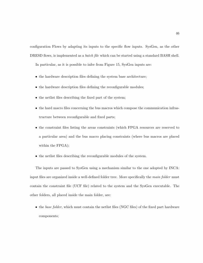
46
configuration Flows by adapting its inputs to the specific flow inputs. SysGen, as the other
DRESD flows, is implemented as a batch file which can be started using a standard BASH shell.
In particular, as it is possible to infer from Figure 15, SysGen inputs are:
• the hardware description files defining the system base architecture;
• the hardware description files defining the reconfigurable modules;
• the netlist files describing the fixed part of the system;
• the hard macro files concerning the bus macros which compose the communication infras-
tructure between reconfigurable and fixed parts;
• the constraint files listing the areas constraints (which FPGA resources are reserved to
a particular area) and the bus macro placing constraints (where bus macros are placed
within the FPGA);
• the netlist files describing the reconfigurable modules of the system.
The inputs are passed to SysGen using a mechanism similar to the one adopted by INCA:
input files are organized inside a well-defined folder tree. More specifically the main folder must
contain the constraint file (UCF file) related to the system and the SysGen executable. The
other folders, all placed inside the main folder, are:
• the base folder, which must contain the netlist files (NGC files) of the fixed part hardware
components;
47
Figure 15. SysGen overview
48
• the HDL folder, which must contain the HDL files of the fix part, of the overall architecture
and of the various reconfigurable modules. Each HDL file must have its own folder into
which it is possible to create ISE projects;
• the recmod folder, which must contain the netlist files (NGC files) of the reconfigurable
hardware modules. Each netlist file must be placed inside a folder with a well-defined suf-
fix: the suffix informs the tool about the reconfigurable area into which the reconfigurable
module must be placed;
• the top folder, which must contain the HDL file of the overall system architecture (i.e.
an HDL file in which there is a fix part instance, several bus macro instances and one
or more reconfigurable modules instances) along with the hard macro (NMC files) of the
communication infrastructure.
After a first SysGen phase checking the input correctness, the tool analyzes the input content
and the available system tools. On the basis of this analysis SysGen will be able to infer if there
are available flows which can make the system partially reconfigurable. For example, if the ISE
version available is not among the supported ones, then SysGen will inform the user that it is
not possible to procede since there are no compatible vendor tools; if the constraint file specifies
reconfigurable area vertical dimensions which do not correspond to the device vertical height,
then the flow based on the module-based partial reconfiguration will be discarded.
After the analysis phase the tool makes use of the compatible flow or ask to the user which
flow must be used if more than one flow is compatible. Another possible tool outcome is an
error message saying that there are no flow available for the specified system in relation to the

49
installed vendor tools. In order to properly use the available flow, several conversion interfaces
are embedded with SysGen; they are able to convert the SysGen inputs to the specific flow
inputs.
Next Chapter will show the application of the entire Caronte flow, including the new SysGen
tool, on an industrial case study.
CHAPTER 4
CASE STUDY
This Chapter describes the industrial application developed during this thesis work, along
with the issues faced and how they were overcame. The external institution which provided the
system specification was Inpeco S.p.a., a company involved in the clinical laboratory automa-
tion market; basically it provides Information Technology solutions which improve laboratory
processes and operations. The main reason that leads Inpeco to ask for the DRESD team
collaboration is the interest they have on Reconfigurable Computing techniques; as a matter
of fact, these techniques are widely diffused in several medical fields and clinical automation is
part of them.
The following Sections are focused on the process of realizing such industrial application.
In particular Section 4.1 reports the Inpeco system specification, explaining in detail the char-
acteristics of the system to be developed. Section 4.2 describes how the system is modeled
within Simulink R© using the methodology proposed in Chapter 2. Section 4.3 shows the system
implementation as a dynamic reconfigurable application, obtained using the various tools devel-
oped by the DRESD Team. In the end, Section 4.4 shows a comparison between the dynamic
reconfigurable implementation of the system and its static implementation.
50
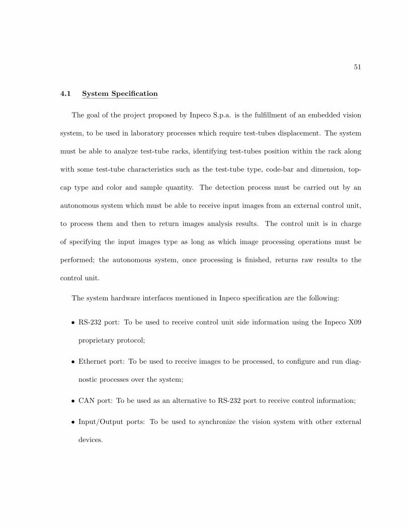
51
4.1 System Specification
The goal of the project proposed by Inpeco S.p.a. is the fulfillment of an embedded vision
system, to be used in laboratory processes which require test-tubes displacement. The system
must be able to analyze test-tube racks, identifying test-tubes position within the rack along
with some test-tube characteristics such as the test-tube type, code-bar and dimension, top-
cap type and color and sample quantity. The detection process must be carried out by an
autonomous system which must be able to receive input images from an external control unit,
to process them and then to return images analysis results. The control unit is in charge
of specifying the input images type as long as which image processing operations must be
performed; the autonomous system, once processing is finished, returns raw results to the
control unit.
The system hardware interfaces mentioned in Inpeco specification are the following:
• RS-232 port: To be used to receive control unit side information using the Inpeco X09
proprietary protocol;
• Ethernet port: To be used to receive images to be processed, to configure and run diag-
nostic processes over the system;
• CAN port: To be used as an alternative to RS-232 port to receive control information;
• Input/Output ports: To be used to synchronize the vision system with other external
devices.
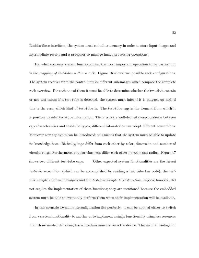
52
Besides these interfaces, the system must contain a memory in order to store input images and
intermediate results and a processor to manage image processing operations.
For what concerns system functionalities, the most important operation to be carried out
is the mapping of test-tubes within a rack. Figure 16 shows two possible rack configurations.
The system receives from the control unit 24 different sub-images which compose the complete
rack overview. For each one of them it must be able to determine whether the two slots contain
or not test-tubes; if a test-tube is detected, the system must infer if it is plugged up and, if
this is the case, which kind of test-tube is. The test-tube cap is the element from which it
is possible to infer test-tube information. There is not a well-defined correspondence between
cap characteristics and test-tube types; different laboratories can adopt different conventions.
Moreover new cap types can be introduced; this means that the system must be able to update
its knowledge base. Basically, taps differ from each other by color, dimension and number of
circular rings. Furthermore, circular rings can differ each other by color and radius. Figure 17
shows two different test-tube caps. Other expected system functionalities are the lateral
test-tube recognition (which can be accomplished by reading a test tube bar code), the test-
tube sample chromatic analysis and the test-tube sample level detection. Inpeco, however, did
not require the implementation of these functions; they are mentioned because the embedded
system must be able to eventually perform them when their implementation will be available.
In this scenario Dynamic Reconfiguration fits perfectly: it can be applied either to switch
from a system functionality to another or to implement a single functionality using less resources
than those needed deploying the whole functionality onto the device. The main advantage for
53
Figure 16. Overview of two test-tube racks
54
Figure 17. Example of test-tube caps
Inpeco S.p.a. is represented by lower FPGAs cost (because the price of FPGAs within the same
family is proportional to resources number). Furthermore, it could also be demonstrated that
system power consumption is lower and that device partial failures can be overcome.
4.2 System Modeling
After a careful analysis of the system specification and some Inpeco S.p.a. clarifications
the modeling process can start. The functionality to be implemented is the mapping of test-
tubes within a rack (rack examples are shown in Figure 16). Inpeco explained that the control
unit is in charge of sending 24 different images composing the rack to the embedded vision
system which must store and analyze them in order to give as result the rack composition.
The system model obviously relies on these images because the analysis must be carried out
starting from them. Figure 18 shows some of the images that have been considered during the
system modeling process; as it can be inferred, the system must be able to detect and process
image portions which are characterized by circular edges. In this way, in fact, it is possible
to identify test-tube taps, circular rings, untapped test-tubes and empty rack slots. These
considerations lead to the need of inserting a circle detection block within the Simulink model.
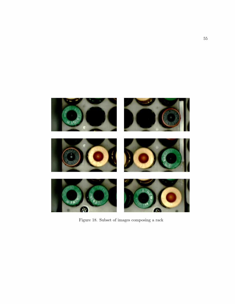
55
Figure 18. Subset of images composing a rack
56
Since there is not such a block in the available Simulink libraries, it has been necessary to
look for already existing problem solutions and to implement the one which fits best. Scientific
literature contains several information about the issue of detecting circles, and more in general,
the issue of detecting arbitrary shapes: the first important document about shape detection is a
1962 US Patent named “Method and Means for Recognizing Complex Patterns” and registered
by P. Hough. Starting from Hough ideas, in (42) the authors explain how to exploit Hough
transform to detect lines and curves while in (43) D. Ballard exposes a method to detect
arbitrary shapes thanks to Hough transform. Even if the article is dated 1987 the method
proposed is still considered among the best ones. Another solution taken into account was
the one presented in (44), which exploits Gradient pair vectors, but in the end it was decided
to use Ballard’s technique. The chosen circle detection algorithm, as many images processing
methods ((45) was the main image processing information source), requires as input a binary
image (i.e. an image composed of boolean pixels); this binary image must be the result of an
edge detection process run over the original image. The algorithm provides as output a list of
circles (center coordinates and associated radius) which can then be used to locate and analyze
every circle shaped image object. Briefly, the Ballard’s algorithm for circle detection assigns an
accumulator to each image pixel; then for every radius that must be taken into account (the
radius range is an algorithm parameter) it firstly reset the accumulators and then it processes
the image looking for edge pixels. When an edge pixel is found the algorithm increments by
one the accumulators relative to every pixel within the image which is at distance <radius>
from the edge pixel. When the whole image is processed, the algorithm looks for accumulators
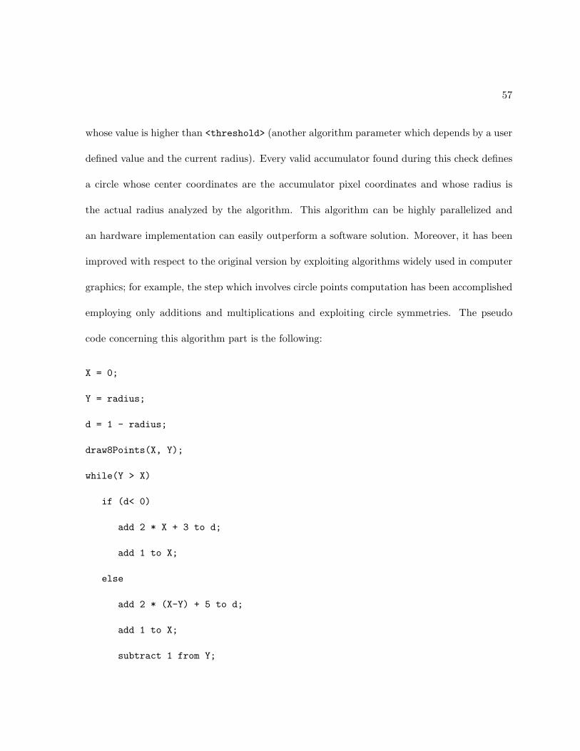
57
whose value is higher than <threshold> (another algorithm parameter which depends by a user
defined value and the current radius). Every valid accumulator found during this check defines
a circle whose center coordinates are the accumulator pixel coordinates and whose radius is
the actual radius analyzed by the algorithm. This algorithm can be highly parallelized and
an hardware implementation can easily outperform a software solution. Moreover, it has been
improved with respect to the original version by exploiting algorithms widely used in computer
graphics; for example, the step which involves circle points computation has been accomplished
employing only additions and multiplications and exploiting circle symmetries. The pseudo
code concerning this algorithm part is the following:
X = 0;
Y = radius;
d = 1 - radius;
draw8Points(X, Y);
while(Y > X)
if (d< 0)
add 2 * X + 3 to d;
add 1 to X;
else
add 2 * (X-Y) + 5 to d;
add 1 to X;
subtract 1 from Y;
58
draw8Points(X, Y);
The algorithm implementation is performed using the Embedded Matlab language in order
to make the newly created Simulink block compatible with Simulink HDL Coder. To continue
system modeling it is necessary to insert an edge detection block (a block capable of providing the
needed binary image to the circle detection block); in this case Simulink provides several edge
detectors but each one of them is not compatible with Simulink HDL Coder. In order to cope
with this new issue the following strategy was adopted: within the Simulink model it was decided
to insert the edge detection block retrieved from the Simulink Image Processing blockset; in this
way it is possible to verify the model using Simulink integrated simulator. Then, just before
the model HDL translation, this block is substituted with already existing VHDL edge detector
cores. The edge detector cores developed in these last years by DRESD team members exploits
either Sobel (46) or Canny (47) edge detection technique. The method developed by J. Canny
is very accurate but also time consuming (48); Figure 19 shows the four phases which compose
Canny technique. The first stage involves smoothing the image by convolving with a Gaussian
filter. This is followed by finding the gradient of the image by feeding the smoothed image
through a convolution operator with the derivative of the Gaussian in both the vertical and
horizontal directions (both the Gaussian mask and its derivative are separable, allowing the 2-D
convolution operation to be optimized). The non-maximum suppression stage finds the local
maxima in the direction of the gradient, and suppresses all the others, minimizing false edges.
The local maxima is found by comparing the pixel with its neighbors along the direction of the
gradient. This helps to maintain the single pixel thin edges before the final thresholding stage.
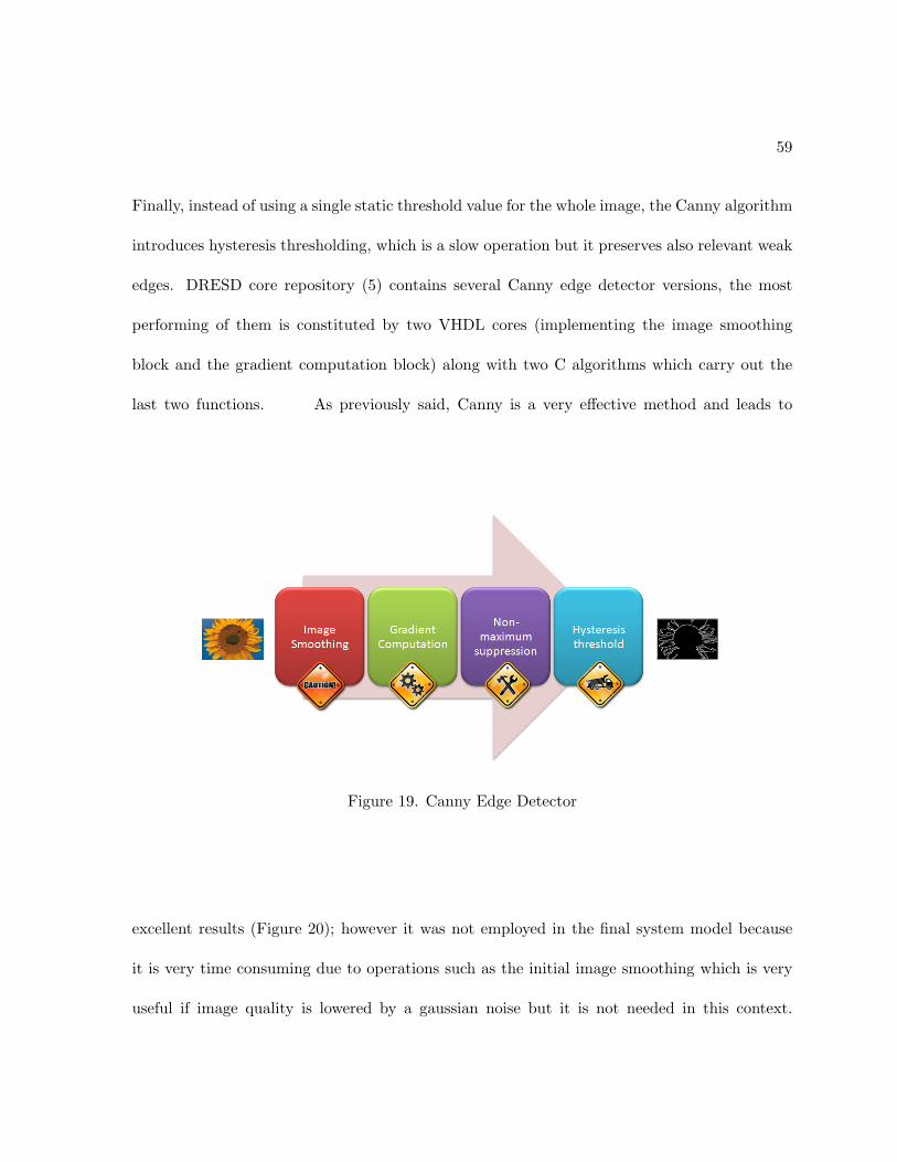
59
Finally, instead of using a single static threshold value for the whole image, the Canny algorithm
introduces hysteresis thresholding, which is a slow operation but it preserves also relevant weak
edges. DRESD core repository (5) contains several Canny edge detector versions, the most
performing of them is constituted by two VHDL cores (implementing the image smoothing
block and the gradient computation block) along with two C algorithms which carry out the
last two functions. As previously said, Canny is a very effective method and leads to
Figure 19. Canny Edge Detector
excellent results (Figure 20); however it was not employed in the final system model because
it is very time consuming due to operations such as the initial image smoothing which is very
useful if image quality is lowered by a gaussian noise but it is not needed in this context.
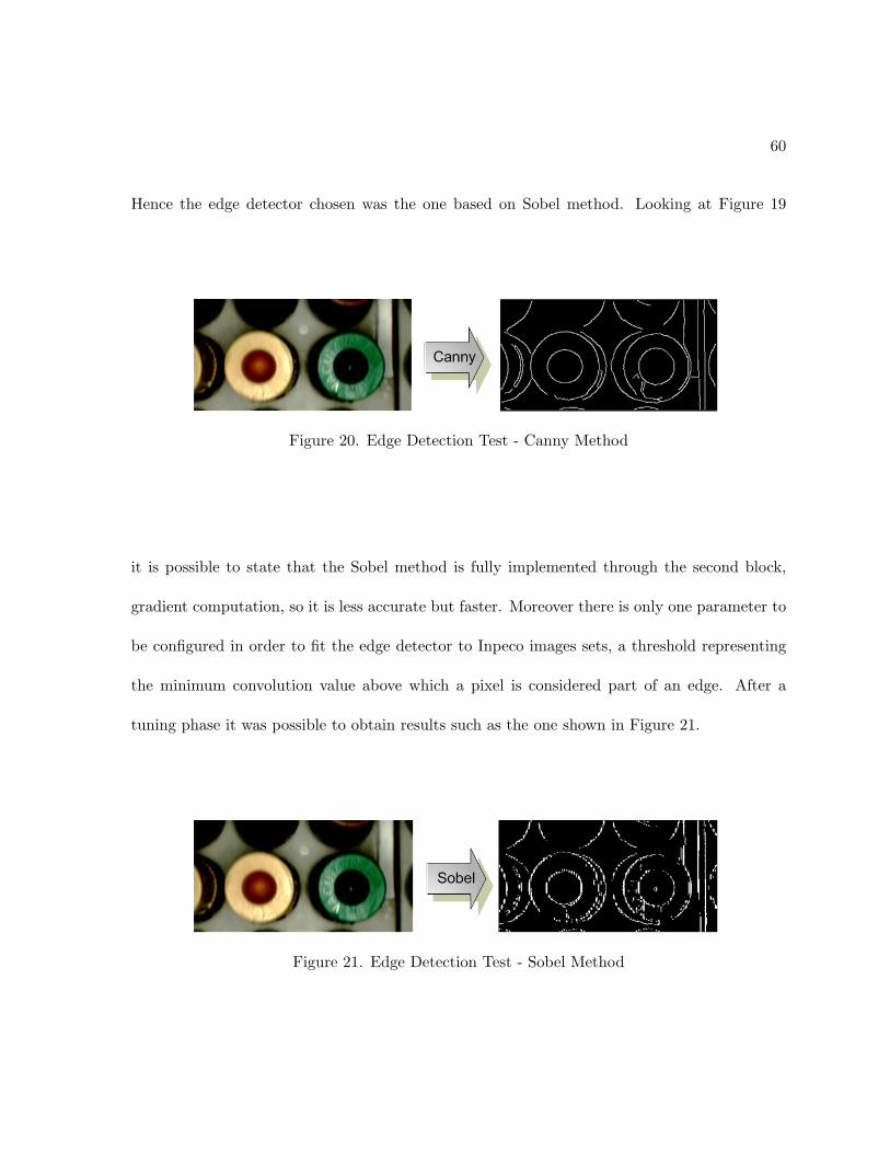
60
Hence the edge detector chosen was the one based on Sobel method. Looking at Figure 19
Figure 20. Edge Detection Test - Canny Method
it is possible to state that the Sobel method is fully implemented through the second block,
gradient computation, so it is less accurate but faster. Moreover there is only one parameter to
be configured in order to fit the edge detector to Inpeco images sets, a threshold representing
the minimum convolution value above which a pixel is considered part of an edge. After a
tuning phase it was possible to obtain results such as the one shown in Figure 21.
Figure 21. Edge Detection Test - Sobel Method
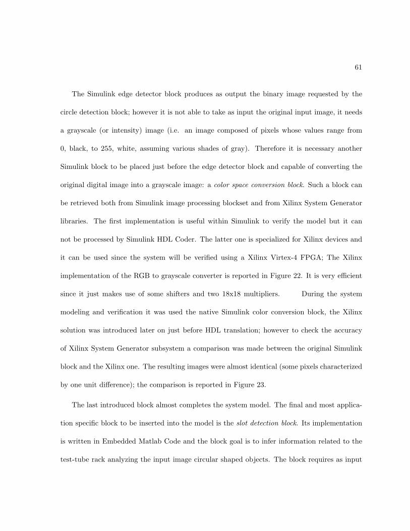
61
The Simulink edge detector block produces as output the binary image requested by the
circle detection block; however it is not able to take as input the original input image, it needs
a grayscale (or intensity) image (i.e. an image composed of pixels whose values range from
0, black, to 255, white, assuming various shades of gray). Therefore it is necessary another
Simulink block to be placed just before the edge detector block and capable of converting the
original digital image into a grayscale image: a color space conversion block. Such a block can
be retrieved both from Simulink image processing blockset and from Xilinx System Generator
libraries. The first implementation is useful within Simulink to verify the model but it can
not be processed by Simulink HDL Coder. The latter one is specialized for Xilinx devices and
it can be used since the system will be verified using a Xilinx Virtex-4 FPGA; The Xilinx
implementation of the RGB to grayscale converter is reported in Figure 22. It is very efficient
since it just makes use of some shifters and two 18x18 multipliers. During the system
modeling and verification it was used the native Simulink color conversion block, the Xilinx
solution was introduced later on just before HDL translation; however to check the accuracy
of Xilinx System Generator subsystem a comparison was made between the original Simulink
block and the Xilinx one. The resulting images were almost identical (some pixels characterized
by one unit difference); the comparison is reported in Figure 23.
The last introduced block almost completes the system model. The final and most applica-
tion specific block to be inserted into the model is the slot detection block. Its implementation
is written in Embedded Matlab Code and the block goal is to infer information related to the
test-tube rack analyzing the input image circular shaped objects. The block requires as input
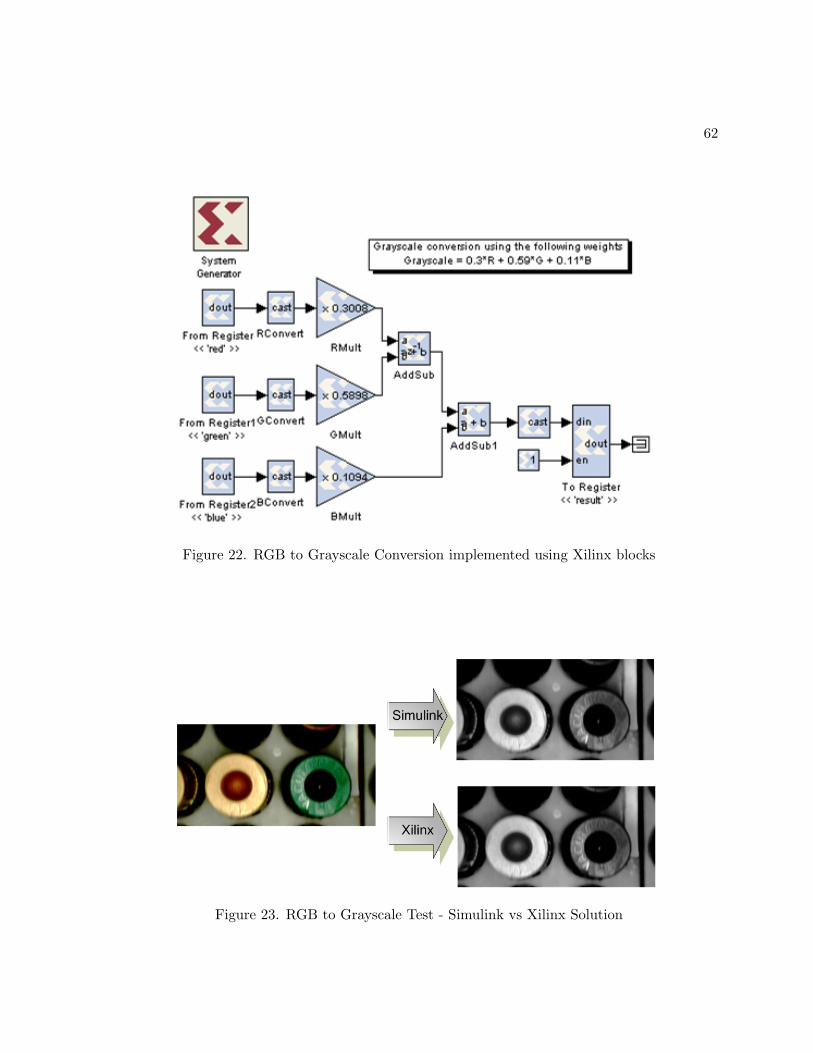
62
Figure 22. RGB to Grayscale Conversion implemented using Xilinx blocks
Figure 23. RGB to Grayscale Test - Simulink vs Xilinx Solution
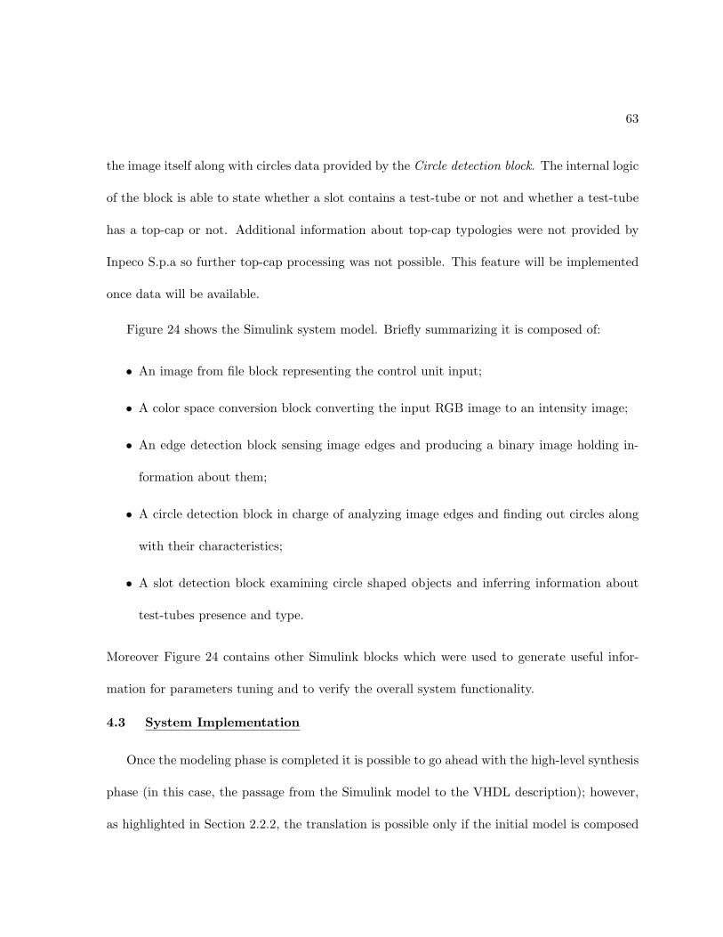
63
the image itself along with circles data provided by the Circle detection block. The internal logic
of the block is able to state whether a slot contains a test-tube or not and whether a test-tube
has a top-cap or not. Additional information about top-cap typologies were not provided by
Inpeco S.p.a so further top-cap processing was not possible. This feature will be implemented
once data will be available.
Figure 24 shows the Simulink system model. Briefly summarizing it is composed of:
• An image from file block representing the control unit input;
• A color space conversion block converting the input RGB image to an intensity image;
• An edge detection block sensing image edges and producing a binary image holding in-
formation about them;
• A circle detection block in charge of analyzing image edges and finding out circles along
with their characteristics;
• A slot detection block examining circle shaped objects and inferring information about
test-tubes presence and type.
Moreover Figure 24 contains other Simulink blocks which were used to generate useful infor-
mation for parameters tuning and to verify the overall system functionality.
4.3 System Implementation
Once the modeling phase is completed it is possible to go ahead with the high-level synthesis
phase (in this case, the passage from the Simulink model to the VHDL description); however,
as highlighted in Section 2.2.2, the translation is possible only if the initial model is composed
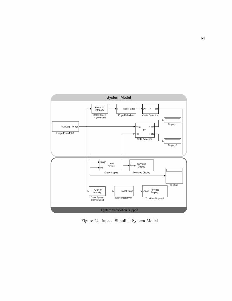
64
Figure 24. Inpeco Simulink System Model
65
of blocks compatible with Simulink HDL Coder. Hence the model reported in Figure 24 has
been modified to comply with Simulink HDL Coder constraints. The final model used to obtain
the VHDL code of the Inpeco application is shown in Figure 25. Once Simulink HDL Coder
Figure 25. Inpeco Simulink System Model Compatible with HDL Coder
constraints are fulfilled, the High Level Modeling Phase (HLMP) of the proposed flow is finished
and the Low Level Implementation Phase (LLIP) starts. As explained in Chapter 4, the tool
developed by The MathWorks places every block hardware description inside a well-defined
66
folder (on the basis of sub-systems nesting) and produces a VHDL “top” file (i.e. a file which
holds information about the system cores instances and about the connections between different
cores). The core hardware descriptions can then be neatly processed using IpGen (36) in order
to produce the needed On-chip Peripheral Bus (OPB) (39) compliant IP-Cores.
Once system IP-Cores are ready, it is possible to create the first static system implementation
that will be compared to the dynamic system implementation leading to the considerations
reported in Section 4.4. The system will be implemented and verified using a Xilinx Virtex-
4 XC4VFX12-FF668-10 FPGA (22) embedded on a Xilinx ML403 evaluation board (49). In
order to obtain the static system implementation it is necessary to add the produced IP-cores to
an Embedded Development Kit (EDK) (38) base architecture. This architecture can be easily
obtained using the EDK Base System Builder (BSB), a tool allowing to define base architecture
components such as processors and input/output interfaces. Specifically, the base architecture
employed to develop the case study application is composed of:
• A MicroBlaze soft processor (50) used to manage system I/O operations and to
synchronize system cores;
• A Local Memory Bus (LMB) (51) BRAM Interface Controller to link the soft processor
to the data and memory stack.
• An On-chip Peripheral Bus (OPB) (39) with an OPB arbiter module to set communication
between the soft processor and the system cores. The processor acts as a OPB master
while all the other cores must be set as OPB slave;
• An OPB RS232 controller to allow data transfer using the development board serial port;
67
• An OPB Double Data Rate (DDR) Synchronous DRAM (SDRAM) controller to provide
the control interface for board DDR SDRAMs.
The custom IP-Cores can be added to this base architecture using another EDK tool, the
Create or Import Peripheral tool. Once the whole architecture is ready the last task that must
be accomplished in order to obtain the system configuration bitstream is writing the control
logic source code; EDK itself offers a development environment which can be employed by
designers to define the control logic using C or C++ as program languages. This case study
required to write an application which must be able to perform the following tasks:
• Initialize the interface controllers and the custom IP-Cores;
• Receive bitmap images through the serial port;
• Derive bitmap images characteristics (height,weight);
• Send control and acknowledgment messages through the serial port;
• Store and Read data from the board DDR memory;
• Provide necessary data to custom IP-cores;
• Synchronize system components.
Once the control logic is ready the bitstream can be created; the process which generates the
final static system implementation bitstream starting from the system hardware description can
be fully performed within EDK. Predefined scripts execute automatically synthesis, translation,
mapping, placing and routing. The EDK block diagram of the architecture created so far is
68
shown in Figure 26. As it is possible to infer, the soft MicroBlaze processor is based on the
classical Harvard architecture; both instruction space and data space are obtained using FPGA
Block RAM (BRAM). The processor is linked to its internal memory through a Xilinx Local
Memory Bus (51). At the same time the processor is connected to an On-chip Peripheral Bus
(39); it acts as a master module while all the other system modules act as slaves.
As pointed out before, the system implementation obtained so far is a classical FPGA im-
plementation. The FPGA bitstream is loaded at device startup and the FPGA configuration
is not altered while the device is working. An alternative solution is represented by the em-
ployment of the partial dynamic reconfiguration technique; the system hardware description
is split up in two parts, one part is composed of hardware modules that can not be changed
at run-time (i.e. the system base architecture) while the other part is composed of hardware
modules which can be substituted at run-time (i.e. custom IP-Cores). This separation can be
obtained using a tool developed by the DRESD Team, ArchGen; this tool requires to organize
the HDL files following a predefined structure. Simulink HDL Coder can be configured to place
its generated VHDL files as requested by ArchGen, but user interaction is still required because
also some EDK generated files must be moved. Once ArchGen processing is finished there will
be a VHDL top file describing the fixed part and a VHDL top file describing the whole system
as the composition of a fixed part and a reconfigurable one. The communication infrastructure
between these two parts is implemented using Bus Macros. The next step concerns VHDL
synthesis; all the components belonging to the fixed part are synthesized together to obtain an
unique netlist. The reconfigurable modules are synthesized separately, each one contributing to
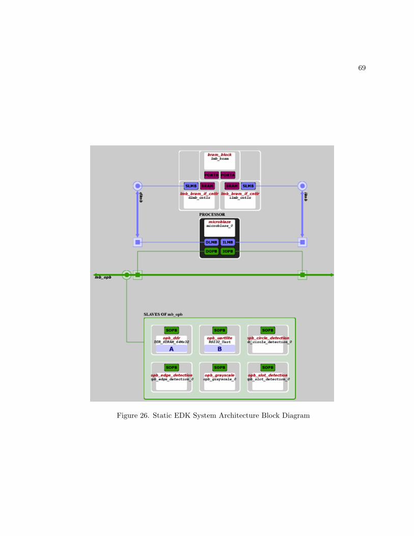
69
Figure 26. Static EDK System Architecture Block Diagram
70
the creation of a single netlist. Besides netlist creation, it is necessary to write a constraints file
holding information about the fixed area and the reconfigurable area size, the signals to pins
assignments and the Bus Macros locations. Once also this phase is finished it is possible to
obtain the bitstreams for the dynamic system implementation. Such bitstreams can be created
using the last DRESD Team tool employed in this thesis work, SysGen, and, in particular, the
INCA flow wrapped by SysGen. The flow is able to create a full FPGA configuration bitstream
that must be loaded at device startup and several partial bitstreams that can be used to change
reconfigurable part functionalities. In the Inpeco case study the FPGA has been partitioned
in two parts, one containing the fixed logic and one containing the reconfigurable logic. The
latter is the implementation of one of the Simulink blocks composing the model in Figure 25.
The reconfiguration bitstreams are loaded onto the device using an external workstation and
change the content of the reconfigurable part, switching from one Simulink block to a different
one.
4.4 Experimental Results
The two system implementations obtained during this thesis work, respectively called static
version and dynamic reconfigurable version, have been described separately in Section 4.3.
This Section is devoted to compare some characteristics of the developed solutions and, in
particular, it is focused on the number of needed resources. In fact, as explained in Chapter 1,
one of the thesis goals is to allow the implementation of large systems using devices with limited
resources; this objective can be achieved thanks to dynamic reconfiguration, that is, deploying
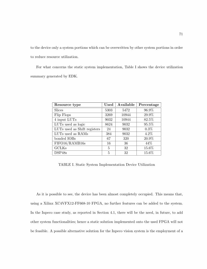
71
to the device only a system portions which can be overwritten by other system portions in order
to reduce resource utilization.
For what concerns the static system implementation, Table I shows the device utilization
summary generated by EDK.
Resource type Used Available PercentageSlices 5303 5472 96.9%Flip Flops 3269 10944 29.9%4 input LUTs 9032 10944 82.5%LUTs used as logic 8624 9032 95.5%LUTs used as Shift registers 24 9032 0.3%LUTs used as RAMs 384 9032 4.2%bonded IOBs 67 320 20.9%FIFO16/RAMB16s 16 36 44%GCLKs 5 32 15.6%DSP48s 5 32 15.6%
TABLE I. Static System Implementation Device Utilization
As it is possible to see, the device has been almost completely occupied. This means that,
using a Xilinx XC4VFX12-FF668-10 FPGA, no further features can be added to the system.
In the Inpeco case study, as reported in Section 4.1, there will be the need, in future, to add
other system functionalities; hence a static solution implemented onto the used FPGA will not
be feasible. A possible alternative solution for the Inpeco vision system is the employment of a
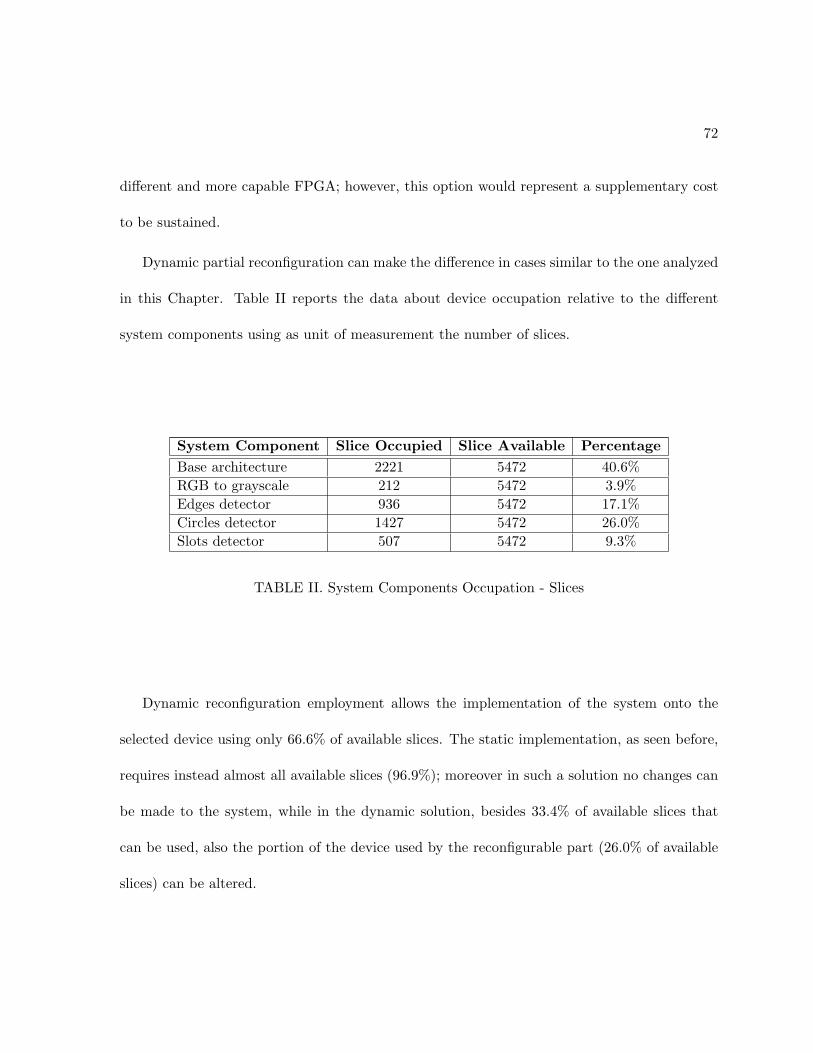
72
different and more capable FPGA; however, this option would represent a supplementary cost
to be sustained.
Dynamic partial reconfiguration can make the difference in cases similar to the one analyzed
in this Chapter. Table II reports the data about device occupation relative to the different
system components using as unit of measurement the number of slices.
System Component Slice Occupied Slice Available PercentageBase architecture 2221 5472 40.6%RGB to grayscale 212 5472 3.9%Edges detector 936 5472 17.1%Circles detector 1427 5472 26.0%Slots detector 507 5472 9.3%
TABLE II. System Components Occupation - Slices
Dynamic reconfiguration employment allows the implementation of the system onto the
selected device using only 66.6% of available slices. The static implementation, as seen before,
requires instead almost all available slices (96.9%); moreover in such a solution no changes can
be made to the system, while in the dynamic solution, besides 33.4% of available slices that
can be used, also the portion of the device used by the reconfigurable part (26.0% of available
slices) can be altered.
73
Such an improvement, however, has a price: the system is slowed down with respect to
the static implementation since the reconfiguration process takes a certain amount of time
before the needed module becomes available. Inpeco S.p.a. must decide whether to adopt
this solution or use more capable FPGAs; the tradeoff is between cost and performance. In
particular it must be pointed out that the developed dynamical solution is based upon external
reconfiguration, hence the performance decrease is considerable; anyway it is possible to adopt
internal reconfiguration to speed up the reconfiguration processes.
CHAPTER 5
CONCLUSIONS AND FUTURE WORK
5.1 Final remarks
This thesis work is part of a wider project started in 2004 with a master thesis work of just
one student (52) and which nowadays involves an entire research team, the DRESD (Dynamic
Reconfigurability in Embedded System Design) Team. The thesis work was entirely developed
at the Politecnico di Milano Microarchitecture laboratory and aimed at introducing model-
based design in DRESD design flows for dynamic reconfigurable FPGA based systems. In
order to achieve such a result this thesis work required to study the principles at the basis
of model-based design and the development environments which rely on model-based design.
In particular it was decided to make use of Simulink R© by The MathWorks, since it is the
most widespread model-based design development environment and since it supports high-level
synthesis of models constituted by a well-defined subset of Simulink blocks. Moreover, both
Xilinx and Altera have developed their own Simulink libraries to provide blocks exploiting
specific FPGAs peculiarities.
Within Simulink this work developed two different modeling techniques; the first one, called
Reconfiguration Aware Modeling, allows to model and verify systems relying on Dynamic Recon-
figuration. The dynamic reconfiguration is introduced in the model by following a set of rules
defined by a meta-model. Once the system model is complete it is possible to use Simulink to
74
75
verify system behavior and to check how it reacts during reconfiguration phases; this is achieved
using, for example, Simulink delay blocks to simulate reconfiguration delays. The latter tech-
nique is called Reconfiguration Unaware Modeling ; it basically constraints block diagrams data
flow producing (thanks to Simulink HDL Coder) a system hardware description which can be
processed by DRESD tools in order to obtain a dynamically reconfigurable system. Recon-
figuration Unaware Modeling has been used to model an industrial application committed by
Inpeco S.p.a., an embedded vision system tailored for test-tube recognition. In the developed
use case dynamic reconfiguration was successfully introduced to reduce FPGA resources occu-
pation, leaving a considerable part of the FPGA (33.4% of available slices) ready to be used to
enlarge the developed system or to implement a completely different functionality. Moreover,
an FPGA part (26.0% of available slices) is declared as reconfigurable, that is, its content can
be changed at run-time allowing the implementation of different functions. This strategy leads
to great advantages in term of resources utilization but it reduces system perfomance since
the reconfiguration process takes a certain amount of time to be accomplished. Inpeco S.p.a.
must choose between buying more capable devices or adopting dynamic reconfiguration; the
dynamic reconfiguration adoption reduces perfomance but it makes the system more flexible
and multi-functional.
5.2 Possible enhancements
From the point of view of the model-based design specification the thesis is exhaustive and
does not need further development. A possible interesting work is to design within Simulink a
certain number of applications to demonstrate the specification validity.
76
From the point of view of the case study, several improvements are needed. First of all,
the implemented functionality must be complete by requiring a formal description of possible
test-tube types and then by extending the slot detection block in order to recognize them.
Furthermore, a comparison between a software solution and the hardware solution is needed,
pointing out how much the hardware solution is faster. The actual system implementation
is for sure faster then a possible software solution, however, it can be greatly improved by
introducing cores DMA (Direct Memory Access). Another system enhancement is represented
by the employment of internal reconfiguration; the actual system implementation, in fact, relies
on external reconfiguration which is slower.
BIBLIOGRAPHY
1. Estrin, G.: Organization of computer systems–the fixed plus variable structure com-puter. Proc. Western Joint Computer Conf., Western Joint Computer Conference,New York, pages 33–40, April 1960.
2. Estrin, G.: Reconfigurable computer origins: the ucla fixed-plus-variable (f+v) structurecomputer. IEEE Ann. Hist. Comput., 24(4):3–9, 2002.
3. Compton, K. and Hauck, S.: Reconfigurable computing: a survey of systems and software.ACM Comput. Surv., 34(2):171–210, 2002.
4. Inc., T. M.: Simulink 7.0 - Using Simulink. The MathWorks Inc., September 2006.
5. Team, D.: http://www.dresd.org.
6. Bolchini, C., Miele, A., and Santambrogio, M. D.: Tmr and partial dynamic reconfigu-ration to mitigate seu faults in fpgas. In DFT ’07: Proceedings of the 22nd IEEEInternational Symposium on Defect and Fault-Tolerance in VLSI Systems (DFT
2007), pages 87–95, Washington, DC, USA, 2007. IEEE Computer Society.
7. Inc., X.: Two Flows of Partial Reconfiguration: Module Based or Difference Based,September 2004.
8. Inc., X.: Early Access Partial Reconfiguration Guide. Xilinx Inc., 2006.
9. Patern, F.: Model-Based Design and Evaluation of Interactive Applications. Springer,1999.
10. Corp., M. G.: Modelsim 6.3 SE/PE/LE User Guide. Mentor Graphics Corp.
11. Behboodian, A.: Model based design and fpga implementation with simulink, 2006.
12. Krukowsky, A. and Kale, I.: Simulink/matlab-to-vhdl route for full-custom/fpga rapidprototyping of dsp, 1999.
77
BIBLIOGRAPHY (Continued) 78
13. Grout, I. A.: Modeling, simulation and synthesis: From simulink to vhdl generatedhardware. In SCI 2001: World Multi-Conference on Systemics, Cybernetics andInformatics, 2001.
14. Haldar, M., Nayak, A., Choudhary, A., and Banerjee, P.: A system for synthesiz-ing optimized fpga hardware from matlab. In ICCAD ’01: Proceedings of the2001 IEEE/ACM international conference on Computer-aided design, pages 314–
319, Piscataway, NJ, USA, 2001. IEEE Press.
15. Inc., T. M.: Embedded Matlab Language User Guide. The MathWorks Inc., 2007.
16. Banerjee, P.: An overview of a compiler for mapping matlab programs onto fp-gas. In ASPDAC: Proceedings of the 2003 conference on Asia South Pacific designautomation, pages 477–482, New York, NY, USA, 2003. ACM.
17. Sbarcea, B. and Nicula, D.: Automatic conversion of matlab/simulink models to hdl models,2004.
18. Inc., T. M.: Simulink HDL Coder 1. The MathWorks Inc., September 2006.
19. Mosterman, P. J.: Matlab and simulink for embedded system design, 2007.
20. Inc., X.: Development system reference guide. Xilinx Inc., 2005.
21. Inc., X.: ISE Quick Start Tutorial. Xilinx Inc., 2006.
22. Inc., X.: Virtex-4 user guide. Technical Report ug70, Xilinx Inc., March 2007.
23. Inc., X.: Virtex-4 configuration user guide. Technical Report ug71, Xilinx Inc., January2007.
24. Donato, A., Ferrandi, F., Redaelli, M., Santambrogio, M. D., and Sciuto, D.: Exploit-ing partial dynamic reconfiguration for soc design of complex application on fpgaplatforms. In Proceedings of IFIP VLSI-SOC, October 2005.
25. Ferrandi, F., Santambrogio, M. D., and Sciuto, D.: A design methodology for dynamicreconfiguration: The caronte architecture. In IPDPS ’05: Proceedings of the 19thIEEE International Parallel and Distributed Processing Symposium (IPDPS’05) -Workshop 3, page 163.2, Washington, DC, USA, 2005. IEEE Computer Society.
BIBLIOGRAPHY (Continued) 79
26. Rana, V., Santambrogio, M. D., and Sciuto, D.: Dynamic reconfigurability in embeddedsystem design. In ISCAS, pages 2734–2737. IEEE, 2007.
27. Weisensee, A. and Nathan, D.: A self-reconfigurable computing platform hardware archi-tecture. CoRR, cs.AR/0411075, 2004.
28. Carvalho, E., Calazans, N., Brio, E., and Moraes, F.: Padreh: a framework forthe design and implementation of dynamically and partially reconfigurable sys-tems. In SBCCI ’04: Proceedings of the 17th symposium on Integrated circuitsand system design, pages 10–15, New York, NY, USA, 2004. ACM Press.
29. Bobda, C., Ahmadinia, A., Rajesham, K., Majer, M., and Niyonkuru, A.: Partial con-figuration design and implementation challenges on xilinx virtex fpgas. In ARCSWorkshops, eds. U. Brinkschulte, J. Becker, D. Fey, C. Hochberger, T. Martinetz,C. Muller-Schloer, H. Schmeck, T. Ungerer, and R. P. Wurtz, pages 61–66. VDEVerlag, 2005.
30. Sedcole, P., Blodget, B., Becker, T., Anderson, J., and Lysaght, P.: Modular dynamic recon-figuration in virtex fpgas. Computers and Digital Techniques, IEE Proceedings-,153(3):157–164, 2006.
31. Inc., T. M.: Real-Time Workshop 7. The MathWorks Inc., September 2007.
32. Inc., T. M.: Link for ModelSim 2 User Guide. The MathWorks Inc., September 2006.
33. Inc., X.: System Generator for DSP 9.2, User Guide. Xilinx Inc., October 2007.
34. Corp., A.: DSP builder 7.2 Reference Manual. Altera Corp., October 2007.
35. Papademetriou, K. and Dollas, A.: A task graph approach for efficient exploitation ofreconfiguration in dynamically reconfigurable systems. In FCCM ’06: Proceedingsof the 14th Annual IEEE Symposium on Field-Programmable Custom ComputingMachines (FCCM’06), pages 307–308, Washington, DC, USA, 2006. IEEE
Computer Society.
36. Murgida, M., Panella, A., Rana, V., Santambrogio, M. D., and Sciuto, D.: Fast ip-core gen-eration in a partial dynamic reconfiguration workflow. In 14th IFIP InternationalConference on Very Large Scale Integration - IFIP VLSI-SOC, pages 74–79, 2006.
BIBLIOGRAPHY (Continued) 80
37. Giorgetta, M., Santambrogio, M. D., Spoletini, P., and Sciuto, D.: A graph-coloringapproach to the allocation and tasks scheduling for reconfigurable architectures. InIFIP VLSI-SOC 2006, pages 24–29, 2006.
38. Inc., X.: Embedded Development Kit EDK 8.2i. Xilinx Inc., 2006.
39. Corporation, I.: On-Chip Peripheral Bus, Architecture Specifications (Version 2.1), 2001.
40. Montone, A. and Piazzi, A.: YaRA: un’Architettura Riconfigurabile Basata sull’ApproccioMonodimensionale. Master’s thesis, Politecnico di Milano, 2006.
41. Vecchio, E.: Definizione di un Flusso per la Generazione Automatica di ArchitettureRiconfigurabili. Master’s thesis, Politecnico di Milano, 2006.
42. Duda, R. O. and Hart, P. E.: Use of the hough transformation to detect lines and curvesin pictures. Commun. ACM, 15(1):11–15, 1972.
43. Ballard, D. H.: Generalizing the hough transform to detect arbitrary shapes. Readings incomputer vision: issues, problems, principles, and paradigms, pages 714–725, 1987.
44. Rad, A. A., Faez, K., and Qaragozlou, N.: Fast circle detection using gradient pair vectors.In DICTA, eds. C. Sun, H. Talbot, S. Ourselin, and T. Adriaansen, pages 879–888.CSIRO Publishing, 2003.
45. Phillips, D.: Image Processing in C: Analyzing and Enhancing Digital Images. 2004.
46. Duda, R. and Hart, P.: Pattern Classification and Scene Analysis. John Wiley and Sons,1973.
47. Canny, J.: A computational approach to edge detection. IEEE Trans. Pattern Anal. Mach.Intell., 8(6):679–698, 1986.
48. Corporation., A.: Edge Detection Reference Design. Altera Corporation., October 2004.
49. Inc., X.: Ml401/ml402/ml403 evaluation platform user guide. Technical Report ug80,Xilinx Inc., May 2006.
50. Inc., X.: MicroBlaze Processor Reference Guide (EDK8.2i). Technical Report ug081, XilinxInc., 2006.

BIBLIOGRAPHY (Continued) 81
51. Inc., X.: LMB BRAM Interface Controller Data Sheet (v2.10a). Technical Report ds452,Xilinx Inc., December 2006.
52. Santambrogio, M. D.: Dynamic Reconfigurability in Embedded System Design – a Modelfor the Dynamic Reconfiguration. Master’s thesis, University of Illinois at Chicago,2004.
VITA
Personal Information
Date of Birth May, 02th 1983
Place of Birth Bergamo (BG), Italy
Citizenship Italian
Languages: Italian (native), English (fluent), French (elementary)
Home: Via Polaresco 34, 24129 Bergamo (BG), Italy
Phone (home): +39 035 260390
Phone (mobile): +39 338 4311025
E-mail: [email protected]
82
83
Education
January 2008 - present Ph.D. Student in Information Engineering
Politecnico di Milano, Italy
March 2006 - May 2008 M.Sc. in Computer Science
The University of Illinois at Chicago
Final GPA: 4.0/4.0
November 2005 - December 2007 Alta Scuola Politecnica
School of excellence founded by Politecnico di Milano and Politecnico di Torino
September 2005 - December 2007 Laurea Specialistica degree (equivalent to M.Sc.) in
Computer Engineering
Politecnico di Milano
Grade: 110/110 cum laude (top 5%)
September 2002 -July 2005 Laurea degree (equivalent to Bachelor) in Computer En-
gineering
Politecnico di Milano
Grade: 110/110 cum laude (top 5%)