Modeling issues and possible solutions in the design of ... · Modeling issues and possible...
25
DesignCon 2008 Modeling issues and possible solutions in the design of high speed systems with signals at 20Gb/s Antonio Ciccomancini Scogna, CST of America [[email protected] ] Jianmin Zhang, Cisco Systems [[email protected] ] Kelvin Qiu, Cisco Systems [[email protected] ] Qinghua Bill Chen, Cisco Systems [[email protected] ]
Transcript of Modeling issues and possible solutions in the design of ... · Modeling issues and possible...

DesignCon 2008
Modeling issues and possible solutions in the design of high speed systems with signals at 20Gb/s Antonio Ciccomancini Scogna, CST of America [[email protected]] Jianmin Zhang, Cisco Systems [[email protected]] Kelvin Qiu, Cisco Systems [[email protected]] Qinghua Bill Chen, Cisco Systems [[email protected]]

Abstract In high speed digital systems with signals at 20 Gb/s, standard approaches used to study the signal integrity at PCB and package level are not valid anymore. IBIS models are no longer accurate and H-spice transient simulations face convergence and stability problems. With the increased operational frequency the metal losses of standard transmission lines at PCB level are not only related to the material characteristic, but they are also related to effects like surface roughness and tapered cross section. Another important issue is the preservation of passivity and causality related to the inaccurate material characterization of the electromagnetic models. How to address these problems? In the present paper some answers will be provided by considering few simple test cases as well as more complex multilayer PCBs. Electromagnetic models are discussed and validated by means of numerical methods, analytical formulation and/or measurements. A practical workflow and design rules for the analysis of differential signals in multilayer PCB is also proposed. Author(s) Biography Antonio Ciccomancini Scogna received the PhD degree in Electrical Engineering from University of L’Aquila, Italy. His main interests are EMC numerical modeling and Signal Integrity analysis in high-speed digital systems. In 2004 he received the CST University Publication Award for the use of the FIT in SI applications and in 2007 he was awarded as finalist at DesignCon. Currently he is senior application engineer at CST of America. He is a member of IEEE, ACES, EMC TC-9 and TC-10 Committees Jianmin Zhang received his BSME from Southeast University, Nanjing, China, and his MSEE/PhD from University of Missouri-Rolla with Electromagnetic Compatibility Laboratory in 2003 and 2007, respectively. In February 2007, he joined CISCO Systems, San Jose, CA, as a Sr. Hardware Engineer, where he is involved in board and package design/layout for signal integrity and power integrity for high-speed interconnects modeling and analysis Kelvin Qiu received his BS and MS in Electrical Engineering from Nanjing University, Nanjing, China, and his MSEE in Computation Electromagnetics from Clemson University, SC, 1995. He joined CISCO Systems in 1998, as Sr. Signal Integrity Engineer, where he is involved in board and ASIC level signal integrity and power integrity analysis and modeling Qinghua Bill Chen is a senior engineering manager with Cisco systems Inc., working on high speed high performance networking product R&D. Previously he worked for Andiamo systems Inc as manager and technical leader, in charge of high speed signal integrity activities. He worked also for RFI, Nplab and Texas Instruments Inc. as technical leader / sr. design engineer working on high speed IC/system designs. Dr. Chen earned his Ph.D. from Texas A& Univ and his MSEE and BSEE from Tsinghua Univ. Beijing, China

Introduction The actual trend on the silicon industry toward higher levels of integration generates chips with densities of tens of millions of transistors. Consequently the signal switching frequency on the modem digital equipment is well beyond the gigahertz range. These high performance systems require high quality point-to-point connections between integrated circuits (ICs) on different printed circuit hoards (PCBs) connected by means of backplanes. When the bandwidth requirement increases, the electrical properties of the interconnections affect and limit the integrity of the traveling digital signals [1]. These phenomena impact also the electromagnetic compatibility (EMC) performances of the system, because corrupted signals can easily increase the unwanted electromagnetic interferences (EMI). Until recently, designers performing high-speed PCB simulations worried mostly about finding IBIS models for driver and receivers, but currently the complexity high speed signals have demanded additional types of models, not only for IC buffers, but also for packages, vias and connectors and this is a really challenging task, therefore 3D field solvers have to be used in order to generate touchstone files or equivalent circuit models to be used in circuit simulator like SPICE. Another important aspect in the design of high speed PCB is the specific dielectric materials with low dielectric losses, to guarantee the quality of the signals traveling on the long traces between ICs. Normally, to characterize the properties of a dielectric material in transmitting high frequency digital signals, test boards are laid-out with traces of different lengths and widths and eye diagrams are measured. This process is not always possible due to economic/time-to market constrains, therefore accurate and reliable equivalent models need to be provided. From the conductors’ point of view, tapered cross section and surface roughness are another important aspect to be considered since the high frequency can produce a consistent increasing of the conductor metal losses as well as impedance variation due to the non-rectangular cross section of the lines. This paper will introduce improved inputs and analysis techniques that will provide designers with the tools and the informations to make informed design and material choices while improving simulation accuracy. Furthermore skin dept and surface roughness (Hammerstad and Jensen analytical model) concepts will be discussed in terms of their impact on the signal integrity, showing how both effects can be taken into account in a 3D field solver with a relatively small computational effort, but still yielding to reasonable accurate results. In particular the results due to a 3D model of surface roughness for a simple stripline model will be compared with the well know Hammerstad and Jensen analytical model and a sensitivity analysis on the different profile for the roughness will be provided as well. Due to inherent advantage on immunity of common mode noise, differential signal routing has to be used for high speed signaling like SERDES, SATA and PCI-X, therefore the “differential signaling” will be discussed. Considering stack-up and cross sectional parameters of signal traces are commonly estimated using 2D field solvers, therefore by assuming the single ended lines of the differential pairs as infinitely long transmission line with no return path discontinuity. Limitation of this approach will be demonstrated and a 3D field solver will be used for the simulation and the analysis for impedance characterization of differential system,

considering return path discontinuities associated with the single-ended and differential signals routed through a complex PCB. Considering the return path discontinuity, performance evaluation of PCBs with differential signal nets in terms of the input differential-mode impedance and input common-mode impedance will be also treated. A multilayer PCB will be used to illustrate the modeling and the simulation methodology. Surface roughness and tapered cross section Due to the rapid increase of circuit complexity and the large scale of integration of the modern electronic devices, the circuit performance is more and more related to the interconnects [2]. Two different kinds of interconnect structures are mainly used in order to propagate signals in ICs and PCBs: microstripline and/or stripline. Stripline is constructed by sandwiching a metallic strip within a dielectric material, whose outer surfaces are metallized. The obvious benefit of the closed structure compared to the microstripline is better protection against external signals and unwanted radiation. Another benefit is the mechanical protection of the inner conductor in a hazardous environment. In the ideal world the conductor of the stripline structure would be perfectly smooth and with a rectangular cross-section. Unfortunately that is not the case in real world, since the conductors have microscopically small dips and grooves on their surface and the cross section is usually a kind of tapered (trapezoid) shape [3-5]. Furthermore copper foils are roughened in order to provide adhesion of the dielectric resin to the conductor in PCBs; adhesion at the interface between conductor and insulator must be very robust due to conditions during the manufacturing process, assembly, and standard usage to which the interconnect is subjected. When the wavelength of the signal has a length comparable to the amplitude of the roughness the attenuation can be relevant and it increases as a function of the frequency. Therefore it must be taken into account when designing stripline structures. Conductor Surface Profile (surface roughness or Rrms) and tapered cross section are related to characteristic impedance of the stripline and attenuation factor. Rrms meaning is root-mean-square (height of the surface bumps) and it represents a measure of surface roughness. A cross view of the test structure used to study the Rrms effect, along with the geometric dimensions, is illustrated in Figure 1a. It is a 400 μm (L) long copper stripline (σ=5.8e7 S/m), the width (W) is 10μm, and the height (h) is 3.5 μm. The dielectric material is Fr4 (εr=4.9) and it is considered loss free, since the purpose is the sensitivity analysis of 1) trapezoidal etching and 2) Rrms. CST Microwave Studio® (CST MWS) [6] is used as 3D field solver to perform the EM numerical simulations. The code is based on the Finite Integration Technique (FIT), an integral method which can be implemented both in time domain or frequency domain. Frequency domain solver and tetrahedral mesh is used in this case for two main reasons: 1) relative small dimensions of the structure, 2) evaluation of the attenuation factor due to conductor loss (α), not available in time domain.

In order to ensure a TEM structure of the electromagnetic field (essential condition for a meaningful interpretation of the scattering matrix), lumped voltage sources are not suitable because they would excite higher order modes. Because of this the TEM excitation has been realized by considering fictitious wave guide structures (waveguide port). Figure 1b illustrates the field mode pattern distribution, the line impedance value and the attenuation factor alpha (α). The detected value of the line impedance is approximately 40 ohm (see Figure 1) while α=13.59 [Neper/m].
(a)
(b)
Figure 1- a): Stripline simulation model used to study Rrms and tapered cross section effect, b): line impedance, alpha and beta value.
Tapered Cross Section Figure 2 is a photograph of a typical board stripline cross-section with in evidences both the tapered edges and the conductor surface profile. Object of the present paragraph is to quantify the effect of the etching reduction according to the test model illustrated in Figure 2. The overall dimensions of the structure are the same of the model presented in Figure 1, but in this case a new parameter is introduced: d, which is the taper variation from the width w.
The DC resistance of the considered interconnect is directly proportional to the length (L), however it does not scale linearly with the width, since the actual width is smaller if compared with the once of Figure 1. The different value from the standard (rectangular cross section) case can be quantified by means of the following relation:
1 lR=σ h(w-d)
(1)
In the previous σ is the conductivity of the stripline, h is the height, w is the width and d is the parameter illustrated in Figure 2. From the previous it is clear that the DC resistance assumes a bigger value if compared with the standard rectangular cross-section. A parameter sweep analysis is executed by varying d in the range 0.2-1.2um. TABLE I report the values of the attenuation factor α, while Fig. 3 illustrates the line impedance variation. How it is possible to see the variation is in the range: 39.9ohm to about 42.1ohm, which means approximately 5-6 %.
Figure 2 - Tapered cross section: real view and simulated cross section model
TABLE I – Attenuation factor
d [um] α [Neper/m] 0.2 12.86 0.4 12.93 0.6 12.94 0.8 12.99 1 13.00
1.2 13.08

Figure 3 - Line impedance variation with the parameter d
When increasing the length of the interconnect the variation is more evident; for example Figure 4 illustrates the insertion loss of 20mm long stripline obtained by cascading 50 blocks of the already simulated model within CST Design StudioTM (CST DS) [6]. It can be observed how the deviation (0.2-0.5dB) on the insertion loss is almost constant along the considered frequency range. The same model is then excited (within CST DS) by means of a rectangular waveform with rise and fall time 0.1ns, hold time 0.2ns and total time 2ns.
Figure 4 – Insertion loss for rectangular and tapered cross-section.
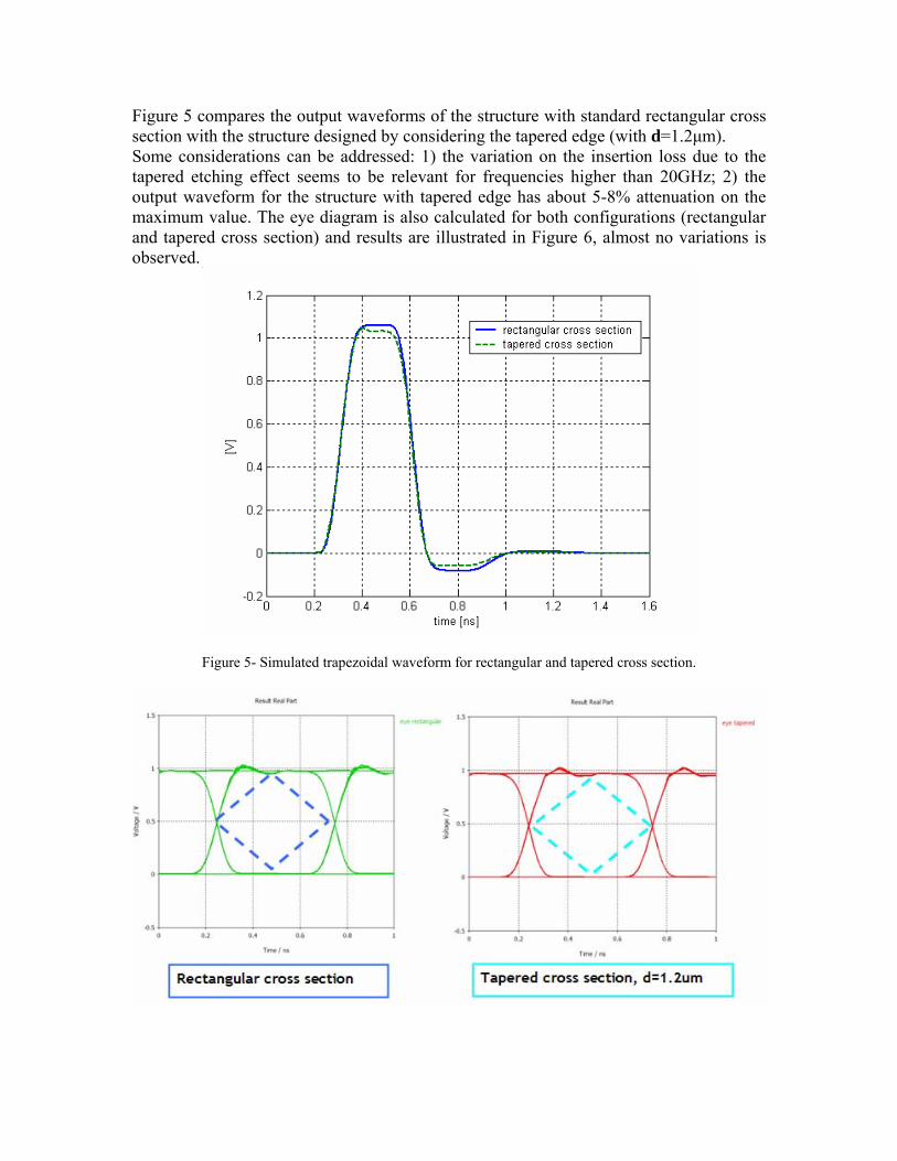
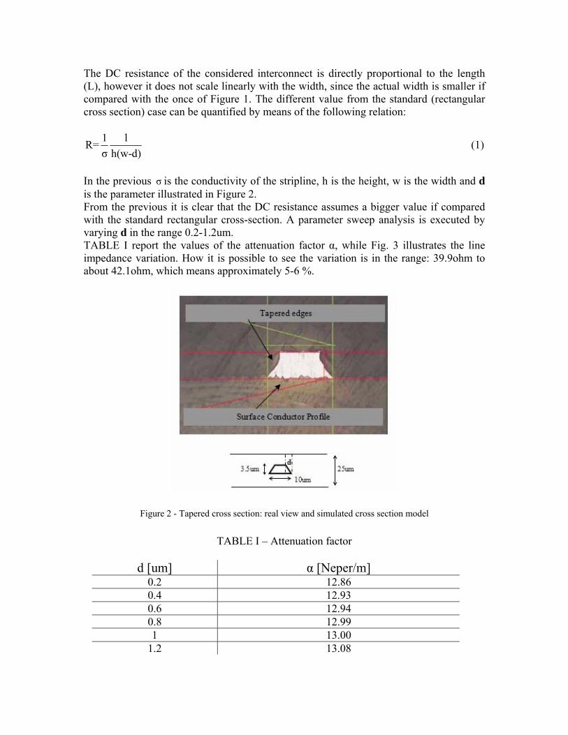
Figure 5 compares the output waveforms of the structure with standard rectangular cross section with the structure designed by considering the tapered edge (with d=1.2μm). Some considerations can be addressed: 1) the variation on the insertion loss due to the tapered etching effect seems to be relevant for frequencies higher than 20GHz; 2) the output waveform for the structure with tapered edge has about 5-8% attenuation on the maximum value. The eye diagram is also calculated for both configurations (rectangular and tapered cross section) and results are illustrated in Figure 6, almost no variations is observed.
Figure 5- Simulated trapezoidal waveform for rectangular and tapered cross section.

Figure 6- Eye diagram for rectangular and tapered cross section. Surface Roughness In this section the incidence of the conductor surface profile (Rrms) on the transmission properties of a stripline is analyzed. Copper foils commonly used in PCB fabrications are made with certain surface characteristics to facilitate the bonding of the copper foil to the dielectric material, with copper surface intentionally roughened to increase the strength of the bond. As the skin depth approaches the dimension of the copper surface roughness, the smooth surface assumption breaks down and the resistance increases at a higher rate than square root of frequency. The increased losses due to surface roughness can be relevant or not, depending on the magnitude of the rectangular step characterizing the surface roughness in relation to the skin depth. The relation between conductor surface profile and loss can be defined by the following relation:
sc
0
Rα Np / mZ w
= (2)
Rs surface resistivity, Z0 impedance of the transmission line and w, trace width. Surface resistance is a material property, partially governed by Rrms, while Z0 and w are both design parameters. Conductive loss is directly proportional to the surface resistance thought the skin effect, as signals travel at the conductor surface at different depths. Different techniques can be incorporated to generate a loss model which include the Rrms effect: 1) adjusting the classical skin effect conductor loss to higher power than the square root of the frequency, 2) increasing the dielectric loss tangent (tanδ) of the dielectric material, due to the fact that for frequencies higher than 1GHz, the difference among copper types are almost linear with respect to the frequency. Both approaches have some issues as explained in [5] so, Hammerstad and Jensen proposed an empirical formula, derived from microstripline measurements, which can be effectively used to model the frequency dependent loss by means of an additional loss term defined as:
'c c srα α K= ⋅ (3)
2
srs
2 ΔK 1 arct g 1.4π δ
⎡ ⎤⎛ ⎞⎢ ⎥= + ⎜ ⎟⎢ ⎥⎝ ⎠⎣ ⎦
(4)
where '
cα is the attenuation for the rough surface, cα is the attenuation for smooth surface, sδ is the skin depth andΔ is the Rrms surface roughness height.
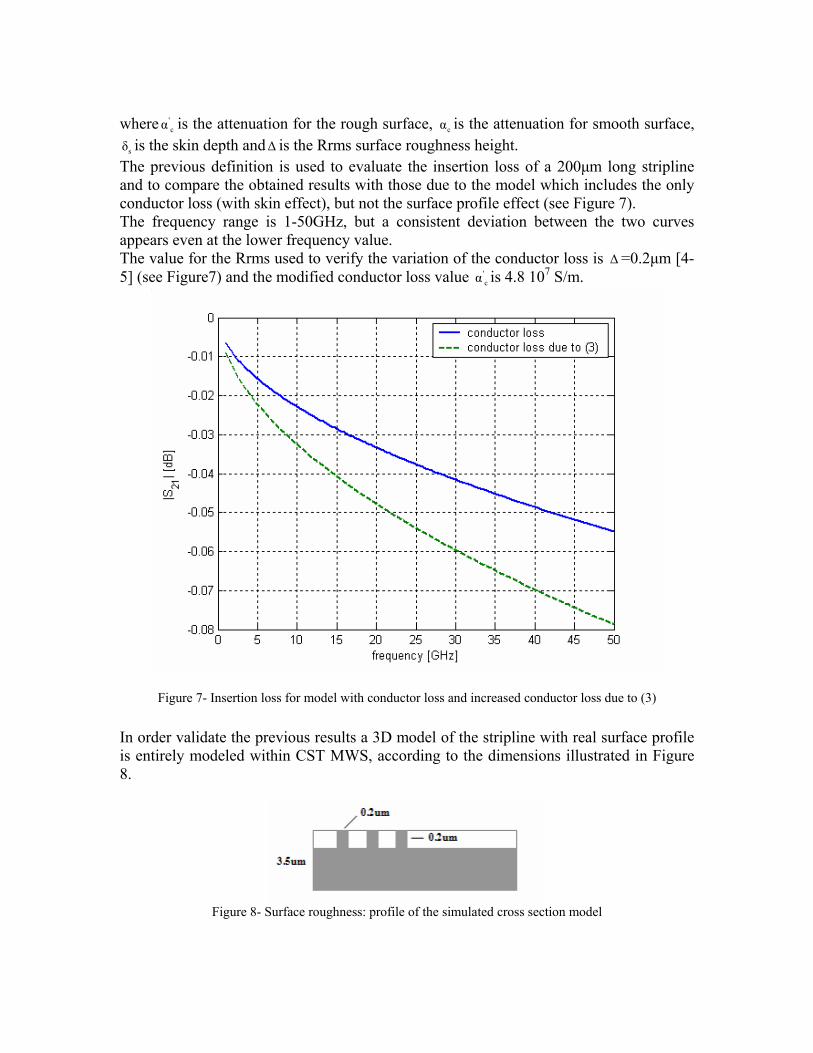
The previous definition is used to evaluate the insertion loss of a 200μm long stripline and to compare the obtained results with those due to the model which includes the only conductor loss (with skin effect), but not the surface profile effect (see Figure 7). The frequency range is 1-50GHz, but a consistent deviation between the two curves appears even at the lower frequency value. The value for the Rrms used to verify the variation of the conductor loss is Δ =0.2μm [4-5] (see Figure7) and the modified conductor loss value '
cα is 4.8 107 S/m.
Figure 7- Insertion loss for model with conductor loss and increased conductor loss due to (3) In order validate the previous results a 3D model of the stripline with real surface profile is entirely modeled within CST MWS, according to the dimensions illustrated in Figure 8.
Figure 8- Surface roughness: profile of the simulated cross section model
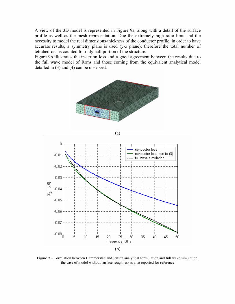
A view of the 3D model is represented in Figure 9a, along with a detail of the surface profile as well as the mesh representation. Due the extremely high ratio limit and the necessity to model the real dimensions/thickness of the conductor profile, in order to have accurate results, a symmetry plane is used (y-z plane); therefore the total number of tetrahedrons is counted for only half portion of the structure. Figure 9b illustrates the insertion loss and a good agreement between the results due to the full wave model of Rrms and those coming from the equivalent analytical model detailed in (3) and (4) can be observed.
(a)
(b)
Figure 9 – Correlation between Hammerstad and Jensen analytical formulation and full wave simulation;
the case of model without surface roughness is also reported for reference

Due to the non-deterministic nature of the surface roughness (different and complex geometries for the surface profile) there is always a certain level of approximation; therefore different models should be developed depending on the surface profile type. Figure 10 shows the different surface roughness profiles used to investigate the incidence on the transmission properties of the considered stripline: a) cylindrical, b) triangular and c) rectangular profile; the geometrical parameters are d, r, h=0.5µm and a=1 µm. The surface roughness is only modelled in the top portion of the stripline in order to reduce the aspect ratio for the full wave simulation. CST DS is used to cascade 4 blocks of the 3D model in order to get the insertion loss of a 1600μm long stripline. The insertion loss profile is represented in Figure 11 and important considerations can be addressed: 1) the level of increase in conductor losses is dependent on the shape and distribution of indentation, 2) the rectangular profile produces different results from the other two cases, therefore Hammerstad and Jensen analytical formulation is only valid for a specific profile, but for more complex geometries a 3D model needs to be realized and a full wave analysis needs to be performed.
Figure 10 - Different surface profiles of Rrms
Figure 11 – Insertion loss for the different surface roughness profiles illustrated in Figure 10.
Dielectric material characterization for accurate modeling A dielectric material is characterized by a complex permittivity defines as the following: ε ε ' jε '' ε '(1 j tan δ)= − = − (5) where ε ' and ε '' are real and imaginary parts and tan δ is the loss tangent. As the behavior of the dielectric material is the response of polarized molecules oscillating to an external electric field, ε ' and ε '' are functions of the frequency. The causality requirement states that such response can not occur earlier than the excitation, further requiring the complex permittivity to satisfy the Krames-Kroning relations:
1 ε ''(ω ')dω 'ε '(ω) 1 Pπ (ω ' ω)
1 ε '((ω ') 1)dω 'ε"(ω) Pπ (ω ' ω)
+∞
−∞
+∞
−∞
− =−
−= −
−
∫
∫
(6)
where P represents the Cauchy value of the integral. From (6) it can be noticed that the real and imaginary part of the permittivity are related to each other, such that the imaginary part can be computed directly if the real part is known, and vice versa. The symmetry of the Fourier transformation indicates that the real part of the permittivity is an even function of the frequency, while the imaginary part is an odd function: ε '( ω) ε '(ω)
ε ''( ω) ε ''(ω)
− =
− = − (7)
Equation (7) implies that the loss tangent, defined as the ratio of the imaginary part to the real part, would be an odd function of the frequency, and should be zero at DC frequency. This means that the assumption of constant loss tangent for all frequencies used by conventional transmission line models violates the causality requirement. The complex permittivity defined by Debye relaxation model satisfies Krames-Kroning relations and therefore produces causal response:
0
Δε 'ε(ω) ε ' jω1ω
∞= ++
(8)
Where ε '∞ the relative permittivity at very high frequencies is, Δε ' is the change in the relative permittivity. Equation (8) predicts a change in the dielectric constant and peak in loss tangent around the frequency 0ω .

It has been widely observed that common PCB dielectric materials exhibit gradual change in dielectric constant over a very broadband frequency range. Such dielectric behavior can be modeled by including many relaxation terms, each localized around different frequency:
Ni
i 1
i
Δε 'ε(ω) ε ' jω1ω
∞=
= ++
∑
In the following an example is provided which shows how an incorrect material characterization produces inaccurate results. The structure consists on a 5.3” long differential stripline and the cross section is illustrated in Figure 12. Numerical data of the dielectric material are available, while for the metal parts, copper (σ=5.8e7S/m) is used for the equivalent electromagnetic model.
Figure 12 – Cross section of the differential stripline model Due to the dimensions of the structure and the broadband frequency range, time domain solver is chosen in order to perform the simulation. A standard Debye model (second order) is used to fit the measured data of the dielectric properties, but the correlation is quite poor (see Figure 13 left side). This is directly reflected on the correlation between the calculated and measured insertion loss (see Figure 14). For this reason a specific macro is developed in VBA in order to guarantee a fitting with preserves the flat behavior of the real and imaginary part of the dielectric material parameters. By doing so, a very good fitting can be provided, as it is possible to see in the right parts of the same Figure 13 (New fitting curve). The comparison between calculated and simulated results in illustrated in Figure 15 and excellent agreement is observed over the all frequency range 0-20Ghz, with a relative error less than 2%.
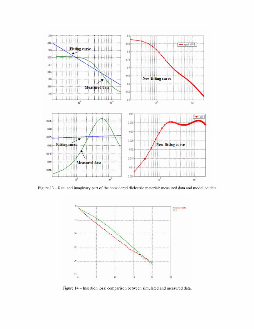
Figure 13 – Real and imaginary part of the considered dielectric material: measured data and modelled data
Figure 14 – Insertion loss: comparison between simulated and measured data.

Figure 15 – Insertion loss: comparison between measured results and simulated results by means of the new
fitting curve for the dielectric material. In order to save simulation time, a different approach is investigated and a very short portion (53 mils long) of the differential model is simulated; the full model is then calculated by consecutively cascading 100 blocks of the 3D simulated model into CST DS (see Figure 16). Even though only the coupling between the blocks and the propagation of higher order modes are neglected, the discrepancy between simulated and measured results became consistent above 4-5 GHz (see Figure 17) and it is found that even the division of the full path into only 4-5 blocks generates quite poor results. This means that from one side the subdivision of the model into sub models can certainly provide relatively faster results, but on the other the accuracy is not always acceptable when dealing with high frequencies.
Figure 16 – Circuit level simulation design view

Figure 17 – Comparison among simulated results (full model), measured results and simulated model obtained by cascading multiple blocks.
It should be mentioned that the problem of the fitting for the dielectric material properties doesn’t existent into the frequency domain since the frequency samples of real and imaginary parts of the dielectric material can be directly used in the simulation. Nevertheless in this case the causality and the passivity are not guaranteed, therefore if the result have to be used in a circuit simulator (for instance in touchstone format) there might be stability and/or convergence problems. Furthermore in the case in which a broadband simulation is required and for more complex models, the frequency domain solver can be very expensive in terms of memory usage and sometimes can even face meshing problems, especially when dealing with models imported directly by EDA platform ( for example Gerber files format). Differential Signaling It is well known [7-8] that differential signaling reduces the noise on a connection by rejecting common-mode interference. At the end of the connection, instead of reading a single signal, the receiving device reads the difference between the two signals (see Figure 18). This is true only in the ideal world; in practice noise induced on the differential lines is likely to appear as common mode. Because the high speed digital system is complex, the discontinuities like vias and bends are inevitably. Differential via hole can be seen as a bifilar transmission lines; it is an

open transmission line, so the distribution of the electromagnetic field is easily affected by the conductor nearby.
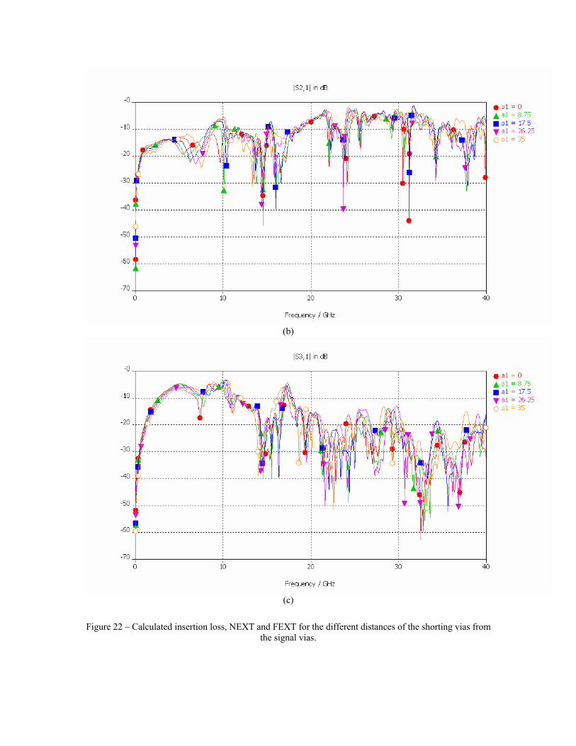
Figure 18 – Example of differential signalling and noise cancellation Usually by considering stack-up a cross sectional parameters of the signal traces different types of impedances (such as even, odd and differential) are estimated using 2D field solvers. These impedance parameters are computed assuming the single-ended lines of the differential pairs as the continuous and infinitely long transmission lines with no return path discontinuity. In reality the differential signal pair routed in a package or boards are not infinitely long continuous transmission lines, due to the discontinuities create by vias, balls and other discontinuities. In order to develop some design guidelines it is critical to accurately characterize the signal traces considering the return path discontinuity, therefore the impedance parameters associated with both single-ended and differential pair of signals should be computed with 3D field simulator. In this section an example is provided by simulating with CST MWS a differential structure in a multilayer PCB (with 26 layers) exported by the corresponding Allegro file. Figure 19 illustrated the *.brd file and the corresponding 3D model of the extracted portion of the board. A comparison between single-ended and differential signals shows (see Figure 20) not only a consistent improvement in the insertion loss, but also a reduction in NEXT and FEXT (10-15dB). Nevertheless this behavior, clear visible till about 20 GHz, is not valid anymore for higher frequency values. In this cases infact a more accurate analysis need to be performed and other solution (rather than the only differential design signaling) should be adopted. For example it is possible to see that by changing the distance of the shorting vias from the signal vias (Figure 21) and the results are illustrated in Figure 22a, where the insertion loss is plotted for 4 different values of distances. If we consider as a figure of merit -3db of loss, we can see an improvement on the bandwidth of more than 3GHz.
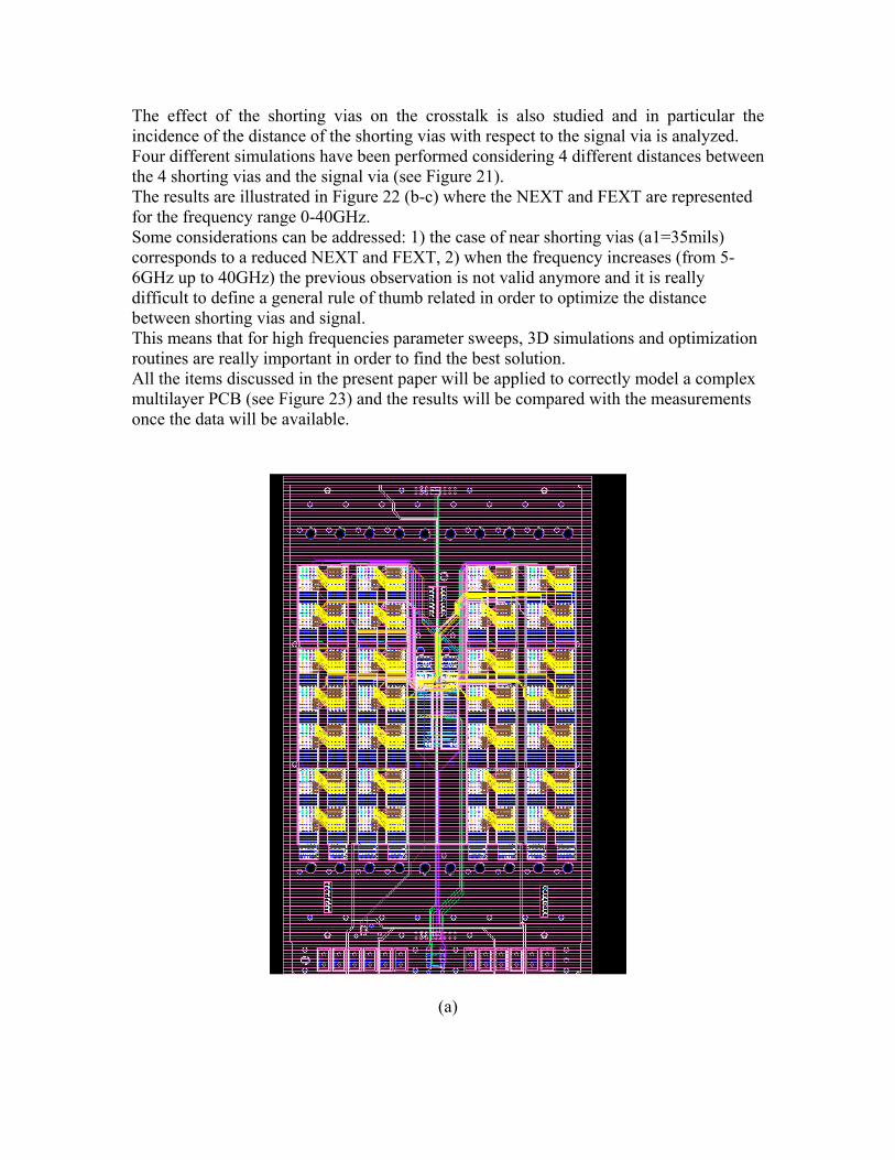
The effect of the shorting vias on the crosstalk is also studied and in particular the incidence of the distance of the shorting vias with respect to the signal via is analyzed. Four different simulations have been performed considering 4 different distances between the 4 shorting vias and the signal via (see Figure 21). The results are illustrated in Figure 22 (b-c) where the NEXT and FEXT are represented for the frequency range 0-40GHz. Some considerations can be addressed: 1) the case of near shorting vias (a1=35mils) corresponds to a reduced NEXT and FEXT, 2) when the frequency increases (from 5-6GHz up to 40GHz) the previous observation is not valid anymore and it is really difficult to define a general rule of thumb related in order to optimize the distance between shorting vias and signal. This means that for high frequencies parameter sweeps, 3D simulations and optimization routines are really important in order to find the best solution. All the items discussed in the present paper will be applied to correctly model a complex multilayer PCB (see Figure 23) and the results will be compared with the measurements once the data will be available.
(a)

(b)
Figure 19 – Allegro view of the multilayer board, b): front view and stack-up view of the corresponding 3D model.

Figure 20 – Insertion loss, NEXT and NEXT: comparison between single-ended signalling and differential
transmission.

Figure 21 – View of the multilayer board with in evidence the 4 shorting vias
(a)
(b)
(c)
Figure 22 – Calculated insertion loss, NEXT and FEXT for the different distances of the shorting vias from
the signal vias.

Figure 23 –Picture of the multilayer PCB which will be analyzed by means of measurements and simulations.
Conclusions The present paper briefly summarizes the most important issues when trying to model high speed systems with signals propagating at 20Gb/s. It is demonstrated how all the basic signal integrity rule of thumbs can easily generate a failure due to inaccuracies, inappropriate and/or too simplified modeling, approximation of important physical behavior. The increased complexity of multilayer PCBs, the reduced distance between signal lines and at the same time the increased operation frequency makes indispensable performing signal integrity studies (NEXT/FEXT types, eye diagram, TDR as well as S-parameters calculation) by means of accurate 3D field simulators. It is also demonstrated how analytic approaches, basic transmission line models and circuit level simulation are often not appropriate for a correct design process. Acknowledgements The authors would like to thank G. Blando with Sun Microsystems for providing the measured data of one of the modeling issue example reported in the paper.

References [1] G. Patel, K. Rothstein, ‘Signal Integrity Characterization of Printed Circuit Board
Traces’, DesignCon 1999 Conference, January 2005. [2] X. Shi, Jian-Guo Ma, Manh Anh Do, Er-Ping Li, “Sensitivity Analysis of
Coupled Interconnects for RFIC Applications”, IEEE Transaction on Electromagnetic Compatibility, vol. 48, November 2006, pag.607-613.
[3] T. Liang, S. Hall, H. Heck and G. Brist, “PCB Transmission Line Modeling for Multi-Gb/s Link Analysis”, DesignCon East 2005.
[4] R. Kollipara et Al., “Practical Design Considerations for 10 to 25 Gbps Coppewr Backplane Serial Links”, DesignCon 2006.
[5] G. Brist, S. Clouser, S. Hall, and T. Liang, “Non-Classical Conductor Losses due to Copper Foil Roughness and Treatment”, 2005 IPC Electronic Circuits World Convention, Feb. 2005.
[6] CST Studio Suite 2008TM - www.cst.com [7] Y. Wang, W. Hong, “Design of differential vias in hung speed digital circuit”, in
Proceedings of APMC, 2005 [8] O. Mandhana, J. Zhao, “Simulation based impedance characterization of high
speed differential systems”, in Proceedings of ECTC, 2007.