Modeling and mitigating pattern andModeling and mitigating...
38
Modeling and mitigating pattern and Modeling and mitigating pattern and process dependencies in nanoimprint lithography lithography 23 June 2011 23 June 2011 Hayden Taylor Singapore-MIT Alliance for Research and Technology formerly based at: Microsystems Technology Laboratories MIT Microsystems Technology Laboratories, MIT
Transcript of Modeling and mitigating pattern andModeling and mitigating...

Modeling and mitigating pattern andModeling and mitigating pattern and process dependencies in nanoimprintlithographylithography23 June 201123 June 2011Hayden Taylor Singapore-MIT Alliance for Research and Technology
formerly based at: Microsystems Technology Laboratories MITMicrosystems Technology Laboratories, MIT

Collaborators and acknowledgements
• Funding • MIT• Singapore-MIT Alliance• Danish National Advanced
Technology Foundation
• Duane Boning• Cai Gogwilt• Matt DirckxTechnology Foundation
• NIL TechnologyKristian Smistrup
• Matt Dirckx• Eehern Wong• Melinda Hale
• Kristian Smistrup• Theodor Nielsen • Brian Bilenberg
• Helpful discussions• Hella Scheerg
• University of California, San Diego• Andrew Kahng
Hella Scheer• Yoshihiko Hirai• Dave White
• Andrew Kahng• Yen-Kuan Wu
2

Spun-on vs droplet-dispensed resist in NIL
Spun-on resist Droplet-dispensed resistresidualresiduallayer
time
– Resist viscosity ≥ 103 Pa.sApplied pressures ~ 5 MPa
– Resist viscosity < 0.1 Pa.sApplied pressures ~ 5 kPa– Applied pressures ~ 5 MPa
– Thermoplastic or UV-curing– Viscous resist squeezing
– Applied pressures ~ 5 kPa– Droplets tailored to pattern– Key figure of merit: filling time
3
q g– Elastic stamp deflections
y g g– Gas trapping and dissolution
S.Y. Chou et al., Appl. Phys. Lett. vol. 67 pp. 3114-3116, 1995S. Fujimori, Jpn. J. Appl. Phys. vol. 48 p. 06FH01, 2009
M. Colburn et al., SPIE 3676, pt.1-2, 379-89, 1999www.molecularimprints.com

NIL pattern and process dependencies have systematic and random componentssystematic and random components
4
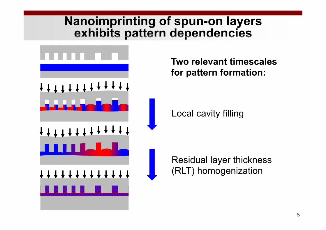
Nanoimprinting of spun-on layersexhibits pattern dependenciesexhibits pattern dependencies
Two relevant timescalesTwo relevant timescales for pattern formation:
Local cavity fillingLocal cavity filling
Residual layer thickness(RLT) h i i(RLT) homogenization
5
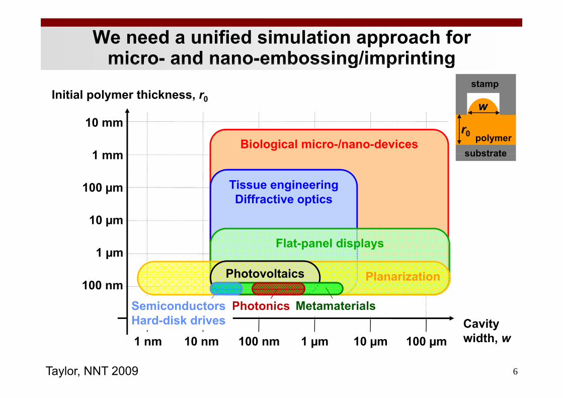
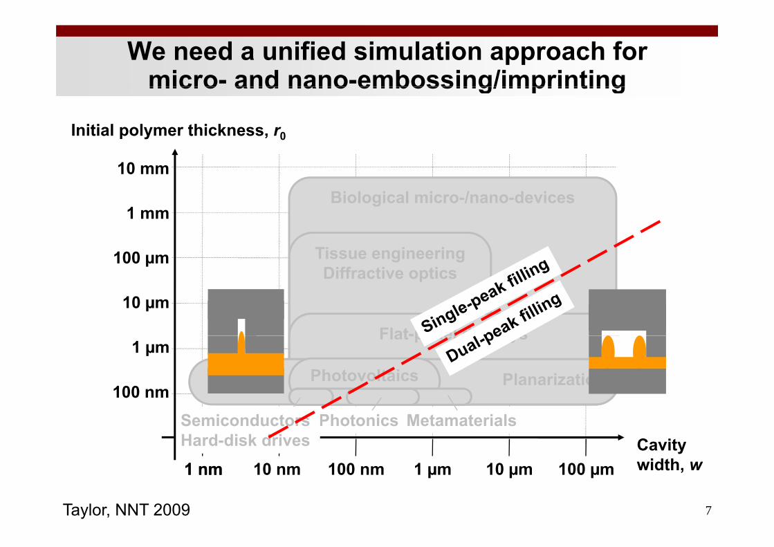
We need a unified simulation approach for micro- and nano-embossing/imprintingmicro and nano embossing/imprinting
stamp
wInitial polymer thickness, r0
polymerpolymersubstrate
w
r010 mm
1 mmBiological micro-/nano-devices
substrate1 mm
100 µm Tissue engineeringDiffractive optics
10 µmDiffractive optics
Flat-panel displays1 µm
100 nm
Flat-panel displays
PlanarizationPhotovoltaics00
Cavity idth
MetamaterialsPhotonicsSemiconductorsHard-disk drives
6
width, w1 nm 10 nm 100 nm 1 µm 10 µm 100 µm
Taylor, NNT 2009
We need a unified simulation approach for micro- and nano-embossing/imprintingmicro and nano embossing/imprinting
Initial polymer thickness, r0
Biological micro-/nano-devices
10 mm
1 mm
Tissue engineeringDiffractive optics
1 mm
100 µmDiffractive optics
Flat-panel displays
10 µm
Flat-panel displays
PlanarizationPhotovoltaics1 µm
100 nm
Cavity idth
MetamaterialsPhotonics00
SemiconductorsHard-disk drives
7
1 nm width, w1 nm 10 nm 100 nm 1 µm 10 µm 100 µm
Taylor, NNT 2009

Key: model impulse response g(x,y,t) of resist layer
Model in time:Model in space:x
Newtonian: impulse
xg Mechanical
impulseresponse constant in time for t > 0
impulse applied uniformly over small region at
Resist
Viscoelastic:
small region at time t = 0
Viscoelastic: impulse response is f i f
Resist
function of time.
8
Substrate
Taylor, NNT 2009. After Nogi et al., Trans ASME: J Tribology, 119 493-500 (1997)
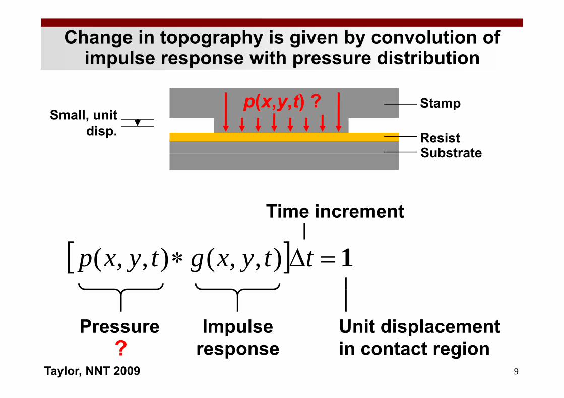
Change in topography is given by convolution of impulse response with pressure distributionimpulse response with pressure distribution
Stampp(x,y,t) ?
ResistSubstrate
pp( ,y, )Small, unit
disp.Substrate
Time increment
1 ttyxgtyxp ),,(),,(
Pressure Impulse Unit displacement
9
presponse
pin contact region?
Taylor, NNT 2009
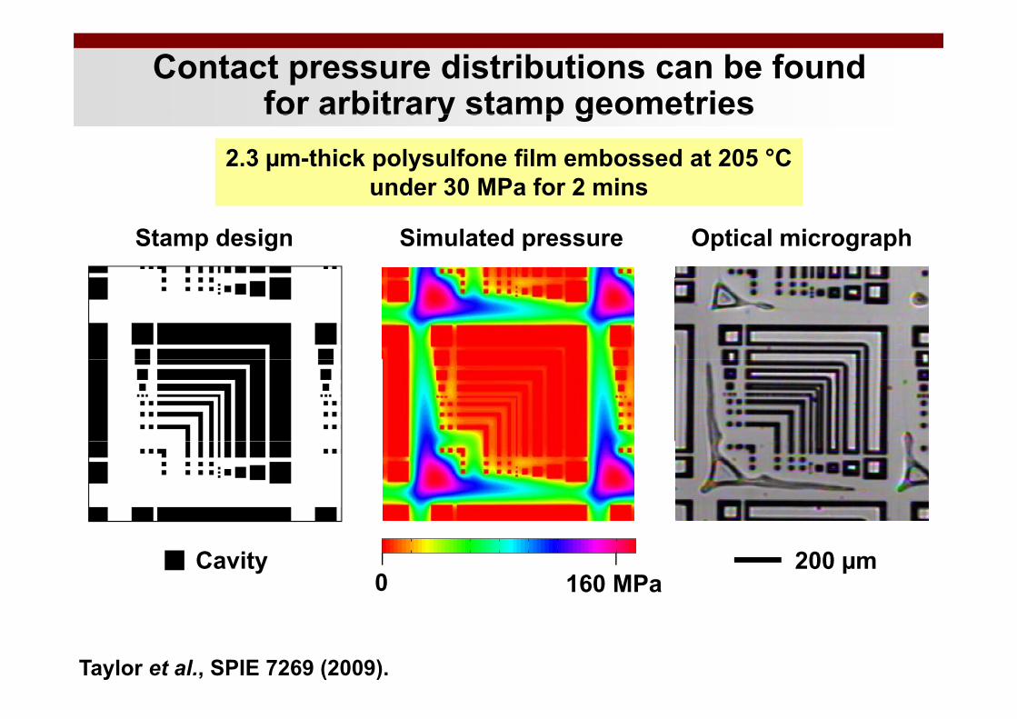
Contact pressure distributions can be found for arbitrary stamp geometrieso a b t a y sta p geo et es
2.3 µm-thick polysulfone film embossed at 205 °C under 30 MPa for 2 mins
Stamp design Simulated pressure Optical micrograph
160 MPa0Cavity 200 µm
Taylor et al., SPIE 7269 (2009).
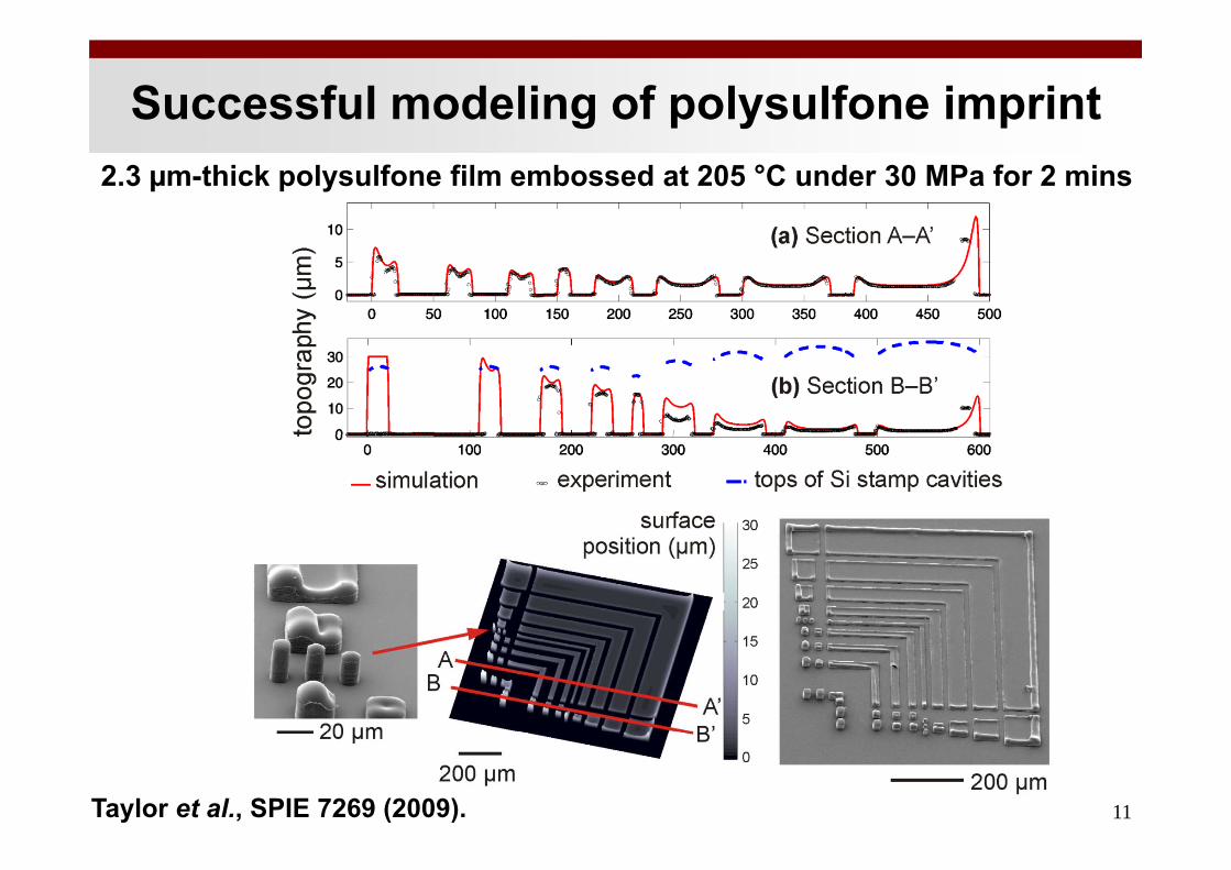
Successful modeling of polysulfone imprint2.3 µm-thick polysulfone film embossed at 205 °C under 30 MPa for 2 mins
11Taylor et al., SPIE 7269 (2009).
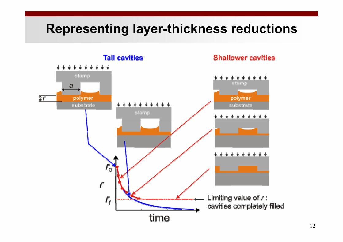
Representing layer-thickness reductions
12
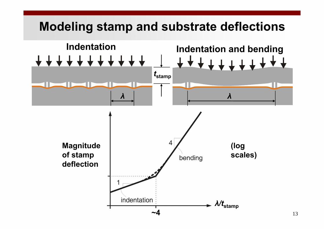
Modeling stamp and substrate deflectionsIndentation Indentation and bending
tstamp
λ λ
Magnitude of stamp deflection
(log scales)
deflection
13
λ/tstamp~4
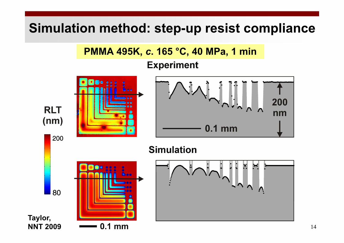
Simulation method: step-up resist compliancePMMA 495K, c. 165 °C, 40 MPa, 1 min
14Taylor, NNT 2009

Abstracting a complex pattern
Local relationships between pressure history and RLT:
Abstractions:
Stamp: point-load response
Resist: impulse response
W f i t l d
15
Wafer: point-load response
HK Taylor and DS Boning, NNT 2009; SPIE 7641 (2010)
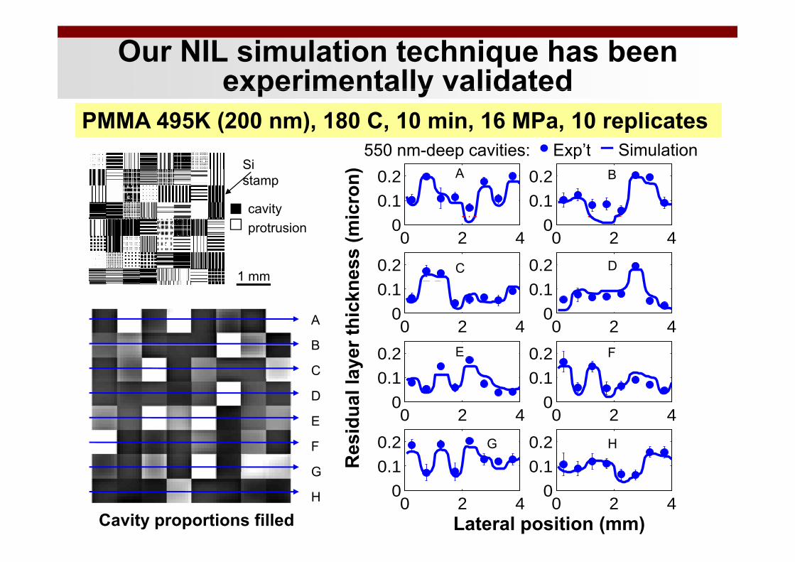
Our NIL simulation technique has been experimentally validated
PMMA 495K (200 nm), 180 C, 10 min, 16 MPa, 10 replicates550 nm-deep cavities: Exp’t Simulation
experimentally validated
Si stamp
cavity0
0.1
0.2
0
0.1
0.2
0
0.1
0.2
0
0.1
0.2
icro
n) A B
550 nm deep cavities: Exp t Simulation
1 mm
protrusion0 2 4
00 2 4
0
0.1
0.2
0.1
0.2
0 2 40
0 2 40
0.1
0.2
0.1
0.2
ness
(mi
C D
0 2 40
0.1
0 2 40
0.1
0.2 0.2
0 2 40
0.1
0 2 40
0.1
0.2 0.2r t
hick
n
A
B
0 2 40
0.1
0.2
0 2 40
0.1
0.2
0 2 40
0.1
0.2
0 2 40
0.1
0.2ua
l lay
erB
C
D
E F
0 2 40
0 2 40
0.1
0.2
0.1
0.2
0 2 40
0 2 40
0.1
0.2
0.1
0.2
Res
iduE
F
G
G H
0 2 40
0.1
0 2 40
0.1
0 2 40
0.1
0 2 40
0.1
Lateral position (mm)Cavity proportions filled
G
H
Simulation time
Simulation time (s) N
104Expected:
time ~ O(N2logN)
1000St 1
100Stamp 1Feature-scale
10
10 100 1000 104Stamp 2
17
Stamp 2AbstractedSimulation size, N
Strengths of the simulation method
• A unified simulation approachA unified simulation approach• Can cope with any layer thickness• Can integrate feature sizes ranging over many orders of magnitude
• Can model any linear viscoelastic material• Speed
• At least 1000 times faster than feature-level FEM
• Implicit periodic boundary conditions are usefulRealistic representation of whole wafer imprint of many chips• Realistic representation of whole-wafer imprint of many chips
• Can use edge-padding for non-periodic modeling
• Suited to quick adaptation for new NIL configurationsSuited to quick adaptation for new NIL configurations• Use to explore the use of flexible stamps and substrates• Explore the imprinting of non-flat substrates
Mi t t i ti ll t ll
18
• Micro-contact printing; roll-to-roll

Varying stamp’s bending stiffness: simulations
Stampthickness:
5 mm
0.5 mm0.12 mmFeatures
200 nm Residual layer
19
4 mmthickness
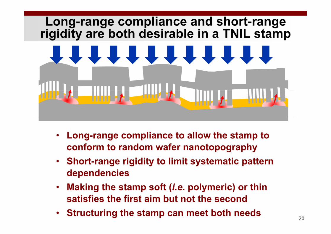
Long-range compliance and short-range rigidity are both desirable in a TNIL stamprigidity are both desirable in a TNIL stamp
• Long-range compliance to allow the stamp to f d f hconform to random wafer nanotopography
• Short-range rigidity to limit systematic pattern d d idependencies
• Making the stamp soft (i.e. polymeric) or thin ti fi th fi t i b t t th d
20
satisfies the first aim but not the second• Structuring the stamp can meet both needs
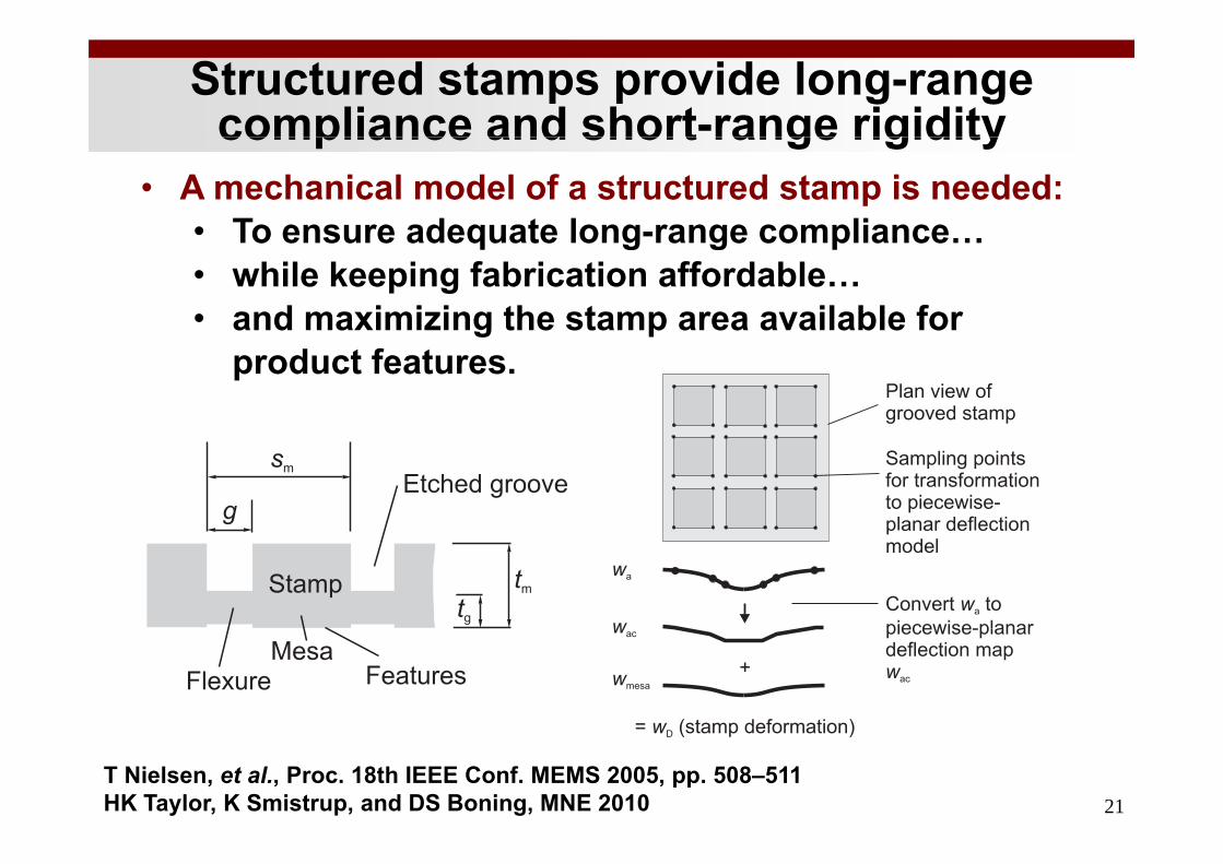
Structured stamps provide long-range compliance and short-range rigiditycompliance and short range rigidity
• A mechanical model of a structured stamp is needed:• To ensure adequate long-range complianceTo ensure adequate long-range compliance…• while keeping fabrication affordable…• and maximizing the stamp area available for g p
product features.
21T Nielsen, et al., Proc. 18th IEEE Conf. MEMS 2005, pp. 508–511 HK Taylor, K Smistrup, and DS Boning, MNE 2010
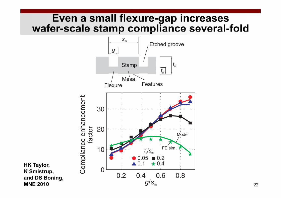
Even a small flexure-gap increases wafer-scale stamp compliance several-foldwafer scale stamp compliance several fold
HK Taylor,
22
HK Taylor, K Smistrup, and DS Boning, MNE 2010

Simulations using a measured wafer topography illustrate long-range compliancetopography illustrate long range compliance
Roughness spectra of three virgin silicon wafersg p g
HK Taylor,
23
HK Taylor, K Smistrup, and DS Boning, NNT 2010

Simulations using a measured wafer topography illustrate long-range compliancetopography illustrate long range compliance
HK Taylor,
24
HK Taylor, K Smistrup, and DS Boning, NNT 2010
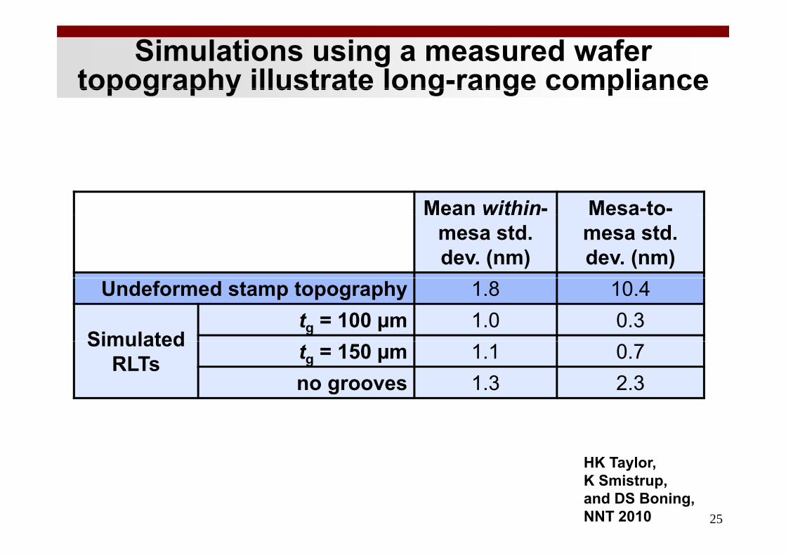
Simulations using a measured wafer topography illustrate long-range compliancetopography illustrate long range compliance
Mean within- Mesa-to-Mean withinmesa std. dev. (nm)
Mesa tomesa std. dev. (nm)
Undeformed stamp topography 1.8 10.4
Simulatedtg = 100 µm 1.0 0.3
SimulatedRLTs tg = 150 µm 1.1 0.7
no grooves 1.3 2.3
HK Taylor,
25
HK Taylor, K Smistrup, and DS Boning, NNT 2010
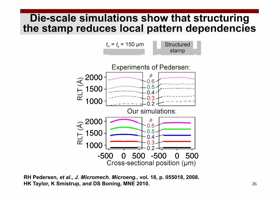
Die-scale simulations show that structuring the stamp reduces local pattern dependenciesthe stamp reduces local pattern dependencies
26RH Pedersen, et al., J. Micromech. Microeng., vol. 18, p. 055018, 2008. HK Taylor, K Smistrup, and DS Boning, MNE 2010.
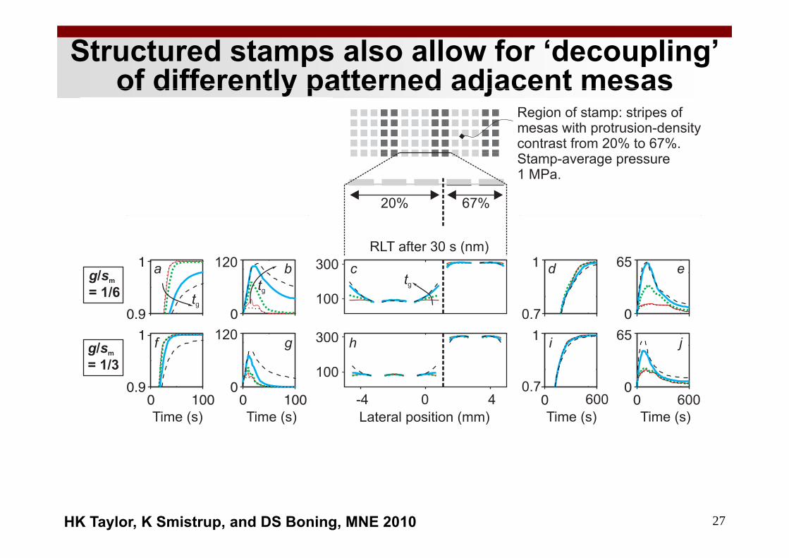
Structured stamps also allow for ‘decoupling’ of differently patterned adjacent mesasof differently patterned adjacent mesas
27HK Taylor, K Smistrup, and DS Boning, MNE 2010

Cavity-filling time depends on length-scale of pattern-density variation, and stamp stiffnesspattern density variation, and stamp stiffness
Lower-density region fills by:
Lateral flow
Lower density region fills by:
Lateral flow and stamp deflection
28HK Taylor, NNT 2010
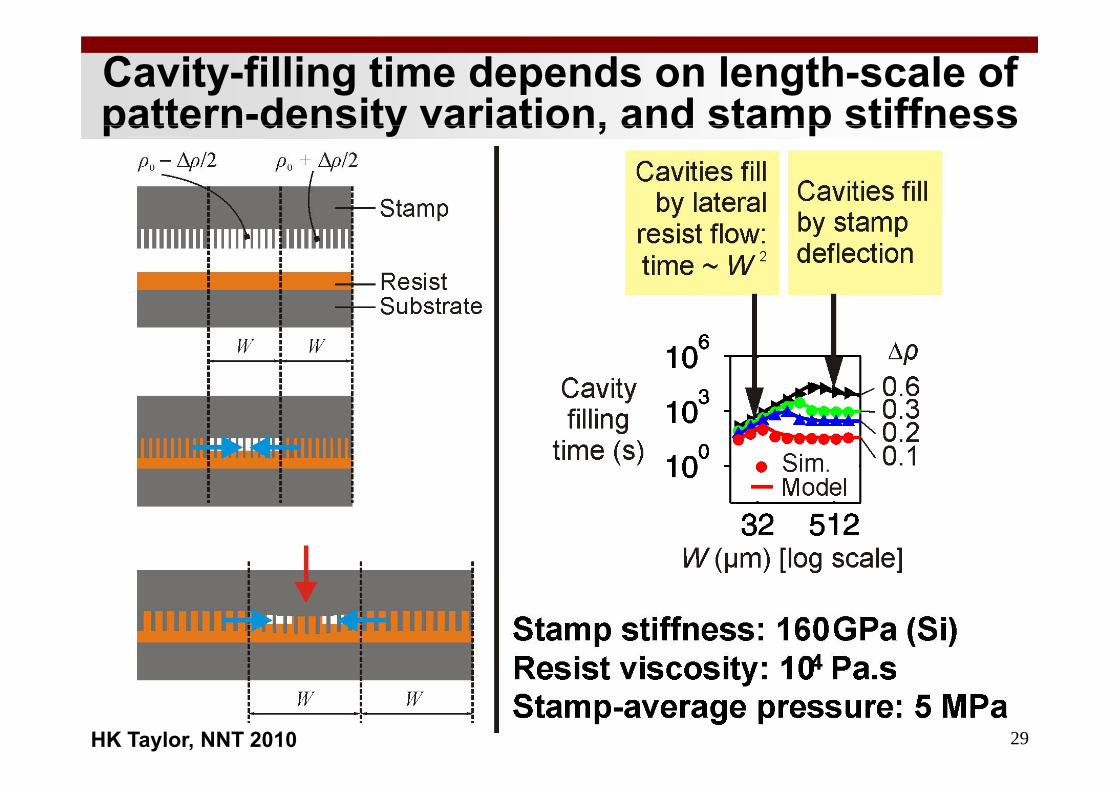
Cavity-filling time depends on length-scale of pattern-density variation, and stamp stiffnesspattern density variation, and stamp stiffness
29HK Taylor, NNT 2010

If imprinted layer is an etch-mask, RLT specifications depend on resist propertiesspecifications depend on resist properties
• (h + rmax)/rmax must be large enough for mask to remain intact throughout etch processg p
• Largest allowable rmax – rmin is likely determined by lateral etch rate and critical dimension specification
30
p
HK Taylor, NNT 2010

Time to satisfy target for RLT uniformity scales as ~W2 for ∆ρ above a thresholdscales as W for ∆ρ above a threshold
W (µm)
31HK Taylor, NNT 2010

We postulate a cost function to drive the insertion of dummy fill into rich designsinsertion of dummy fill into rich designs
N W 2 11
N
i i
ifill
hrhrp
Wt0
2
00
2000
2
21
111
16ˆ
Wi
2
• Abutting windows of size Wi swept over design• ∆ρi is maximal density contrast between abutting ρi y g
windows in any location• Objective is to minimize sum of contributions
from N+1 window sizes
h t i h i ht t
32
• h: protrusion height on stamp• r0: initial resist thickness

We postulate a cost function to drive the insertion of dummy fill into rich designsinsertion of dummy fill into rich designs
N W 2 11
N
i i
ifill
hrhrp
Wt0
2
00
2000
2
21
111
16ˆ
Wi
2
33

A simple density-homogenization scheme offers faster filling and more uniform RLToffers faster filling and more uniform RLT
Characteristic feature pitch (nm)104
Metal 1 of example integrated circuit: min. feature size 45 nm
1
Stamp protrusion pattern density: without dummy fill
103
10
1 103
0 5
102
Predominant feature orientation0.5
0
34
0
100 µm HK Taylor, NNT 2010

A simple density-homogenization scheme offers faster filling and more uniform RLToffers faster filling and more uniform RLT
Density: without fill Density: with fillDesigned protrusion Available for dummy
1 µmDesigned protrusion Available for dummy
1
0.5
350100 µm
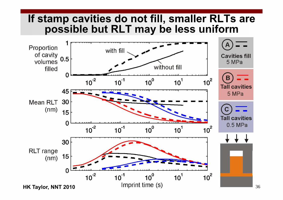
If stamp cavities do not fill, smaller RLTs are possible but RLT may be less uniformpossible but RLT may be less uniform
36HK Taylor, NNT 2010
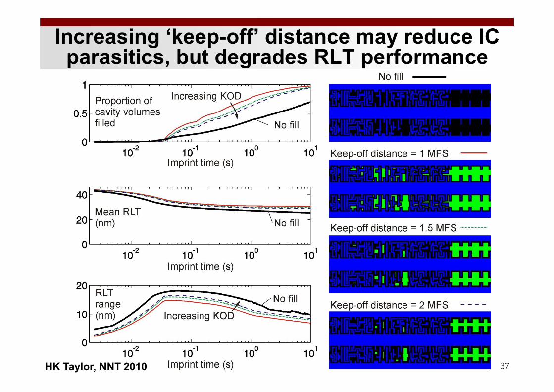
Increasing ‘keep-off’ distance may reduce IC parasitics, but degrades RLT performanceparasitics, but degrades RLT performance
37HK Taylor, NNT 2010

Summary: modeling and mitigation of process and pattern dependencies in NILprocess and pattern dependencies in NIL
Thermal NIL
Modeling Mitigating
Structured stamps: long range
Stamp’s elastic
Resist’splastic
Design rules for pattern densitylong-range
compliance, short range rigidity
elastic deflection
plasticdeformation
P tt
pattern density uniformity; dummy fill insertion
Pattern abstraction
Ongoing: extend to UV-NIL:• Capillary pressures ‘Mechanical • Gas bubble trapping• Droplet spreading
proximity correction’