Modeling and Characterization of Copper Interconnects · Macro IP 45 ° Metal 1 Metal 2 ... 21...
37
CADENCE CONFIDENTIAL 1 CADENCE DESIGN SYSTEMS, INC. Modeling and Characterization of Copper Interconnects Narain Arora [email protected] February 2003
Transcript of Modeling and Characterization of Copper Interconnects · Macro IP 45 ° Metal 1 Metal 2 ... 21...

CADENCE CONFIDENTIAL1 CADENCE DESIGN SYSTEMS, INC.
Modeling and Characterization of Copper Interconnects
Narain Arora [email protected]
February 2003

2 CADENCE CONFIDENTIAL
• Interconnect – an overview • Why copper ?
• What is different in modeling Cu wires • Resistance modeling
• Inductance modeling
• Capacitance modeling
• Full-chip approach
• Silicon Validation
• Model order reduction
• Conclusion
Outline

3 CADENCE CONFIDENTIAL
An Overview • An interconnect is characterized by three elements Resistance R,
Capacitance C, Inductance L, known as interconnect parasitic elements, that are distributed in nature, just like a Transmission lines
• The three parameters R, C, L, are not equally important, depends upon
– Length of the line,
– Signal rise time tr,
– driver impedance Zs, and
– line impedance Z0.
R LC G
RC
LG
Section1 Section N
Transmission lineModel
ts
Zo
01
VoutRs
t
Rs >Zo
tr
td
Vout
1.0
Vout
t
1.0td
trtd
Rs <Zo
4 CADENCE CONFIDENTIAL
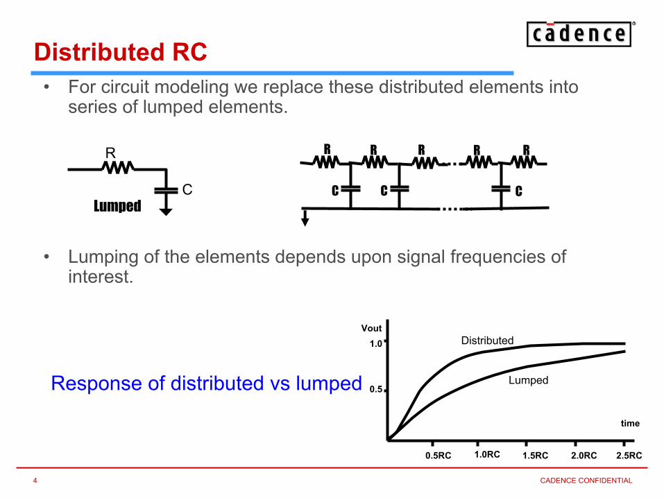
• For circuit modeling we replace these distributed elements into series of lumped elements.
• Lumping of the elements depends upon signal frequencies of interest.
Distributed RC
LumpedC
R
C C
RR
C
R R R
0.5
1.0
1.0RC0.5RC 1.5RC 2.0RC 2.5RC
VoutDistributed
Lumped
time
Response of distributed vs lumped

5 CADENCE CONFIDENTIAL
VLSI Interconnections
• Past 30 years Al has been de facto industry standard as a material for interconnections. – Over the years Al evolved from single layer to multiple levels of
sandwiched Ti/Al-Cu/TiN
• Single layer of dielectric material to multiple dielectrics
ARC(Alloy of Ti)
ρ=3.7x 10⁻⁶ Ω.cm
Al +0.5% Cu
M4
via
siliconM1M2
ILD
Local Line
Global Line
M3
M5
ε2
M3
M2
M1
ε3
ε1

6 CADENCE CONFIDENTIAL
Technology Trends• With ever increasing demand for faster, reliable and higher functionality
chips, transistors have been systematically scaled down in dimensions and so has the interconnects
Source: SIA Roadmap 1997
0.65 0.5 0.35 0.25 0.18 0.13 0.10 µDe
lay (p
s)
454035302520151050
Gate Delay
Interconnect DelayAl + SiO2Interconnect
dominates gate delay
Interconnect dominates gate delay
Speed / Performance - Gate vs interconnect
Total Capacitance
3 micron 0.3 micron
Substrate
Overlap
SubstrateCfr Fringe
LateralCa
CaClt
Substrate
Ca
Clt
Ct=Ca+Cf+Clt
7 CADENCE CONFIDENTIAL
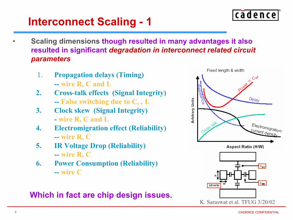
Interconnect Scaling - 1• Scaling dimensions though resulted in many advantages it also
resulted in significant degradation in interconnect related circuit parameters
1. Propagation delays (Timing)-- wire R, C and L
2. Cross-talk effects (Signal Integrity)-- False switching due to Cc , L
3. Clock skew (Signal Integrity) - wire R, C and L
4. Electromigration effect (Reliability) -- wire R, C
5. IR Voltage Drop (Reliability) -- wire R, C
6. Power Consumption (Reliability) -- wire C
Which in fact are chip design issues. K. Saraswat et al. TFUG 3/20/02

8 CADENCE CONFIDENTIAL
IR Drop & Ground Bounce• IR Drop (ground bounce) increases clock skew
– Hold time violations
• IR Drop (ground bounce) increases signal skew
– Setup time violations
CLK
VDD = 1.1V
VDD = 1.17V
VDD = 1.20V
Impacts timing and leads to failed silicon
9 CADENCE CONFIDENTIAL
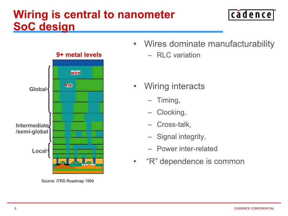
Wiring is central to nanometer SoC design
• Wires dominate manufacturability– RLC variation9+ metal levels
Source: ITRS Roadmap 1999
wire
ViaGlobal
Local
Intermediate/semi-global
• Wiring interacts– Timing, – Clocking, – Cross-talk, – Signal integrity, – Power inter-related
• “R” dependence is common

10 CADENCE CONFIDENTIAL
Cu as Interconnect lines• Cu has ½ the resistance of Al.
• An order of magnitude higher electromigrationresistance
• It has many advantages:
www.Novellus.comMajor process change moving from 180nm technology node to 130nm node was the use of
Cu interconnects and low K dielectrics

11 CADENCE CONFIDENTIAL
Copper Process
• Dual Damascene -- Trench etch profile, Barrier/Seed layer
• Lithography -- Cu wire dimensions are not as drawn
• CMP -- dishing, erosion
line thickness variation
• Result: Cu wire width and thickness becomes function of
– Wire width and spacing
– Wire pattern density
– Wire topography
Barrier layer( TaN)
Cu SiN3
ρ=2.2x 10⁻⁶ Ω.cm
ManufacturedDrawn

12 CADENCE CONFIDENTIAL
Impact of Dishing and Erosion
Lakshminarayan et al. IITS 2001
Dishing and ErosionLayout dependent
Wire Width and Thickness
Resistance
ILD Thickness
Wire Capacitance
Metal Density

13 CADENCE CONFIDENTIAL
Slotting
49.140.2340
13.510.1781
00.15690.1569
Difference
No Slots vsSlots(%)
Results with slots
(Ω)
Resistance w/ no slots
(Ω)
Reduce dishing in wide lines > 2 µm

14 CADENCE CONFIDENTIAL
Metal FillsTo reduce dishing and erosion of the inter-level dielectrics, CMP requires metal lines to be at a certain minimum distance from each other (metal density). This leads to the so called metal fills (dummy metal) - floating metal lines
Dummy metals are of different shape and size.Impact of metal fills is to increase line capacitance by 3-5% depending upon shape, size and proximity of the fills to the line.
Metal fill
Signal Lines

15 CADENCE CONFIDENTIAL
Adjacent Line GroundedCtotal = 155.5fF/m
Adjacent Line FloatingCtotal = 56.24fF/m
Adjacent Line RemovedCtotal = 54.61fF/m
Impact of Grounding Fills
2 34 51

16 CADENCE CONFIDENTIAL
Impact of Cu and low K• It is this proximity effect that is challenging and
necessitated retooling of the design tools.
• Since Cu has ½ of the Al resistance for the same wire dimensions, wire inductance effect becomes more dominant
Z = R + jωL
– Ringing and overshoot - problematic for clocks since glitches can be observed as transitions leading to faulty switching
– Reflections of signals due to impedance mismatch
– Switching noise due to voltage drops - problematic for power distribution network.
• The intra-die variation of the interconnects becomes more pronounced in Cu wires.
Ldidt

17 CADENCE CONFIDENTIAL
Future of Cu• Use of Cu shifts the delay transition point
Optical interconnects ??

18 CADENCE CONFIDENTIAL
Optimized Manhattan Routing
Preferred directionwith optimization Manhattan
Std. Cells
Memory
Macro IP
45°
Metal 1
Metal 2
Metal 3
Metal 4
Metal 5
X-Architecture

19 CADENCE CONFIDENTIAL
Benefits From X-Architecture
10% performance gain AND
20% power reduction AND
30% cost savings
20+% less interconnect
30+% less vias

20 CADENCE CONFIDENTIAL
Manhattan Vs X Architecture:
RISC chip - Manhattan Toshiba First X-architecture design
Presented at ISSCC 2002

21 CADENCE CONFIDENTIAL
Modeling and Characterization of Interconnects
• The software tool that computes the R,C, L of a chip interconnections is called Parasitic Extractor, also known ascircuit level extractor, LPE, etc.
• Modeling:
– Numerical methods, the so called Field Solvers: – provides accurate em field solutions for complex geometry.
– allows the modeling of non-linear, inhomogeneous and anisotropicmaterial
– Analytical / Empirical models
• Characterization:
– Low Frequency Measurement
– Frequency domain S parameter (inductance)
– Test structure verification

22 CADENCE CONFIDENTIAL
• Numerical or Field solver approach uses Maxwell’s Electromagnetic field equations
Methods of modeling R, L, C
tcurl
∂∂
+=DJH
Ampere’s theorem Faraday’s law
EJ ED HB σ=ε=µ= ,,
Constitutive equations
To be solved with initial and boundary conditions
tcurl
∂∂
−=BE
ρ=Ddiv 0div =B

23 CADENCE CONFIDENTIAL
choice of working variables field quantities, potentials, ...
choice of numerical technique FEM, FDM, BEM, ...
choice of matrix solver iterative, direct, multigrid, ...
post-processor interpolation, integration, visualization ...
Filed distribution, circuit parameters
Solutions
Partial differential equations
Physical equations
Numerical computation of EM field
Algebraic equations
Raphael, Maxwell,Quickcap, SAP,Fastcap, FastHenry

24 CADENCE CONFIDENTIAL
Interconnect Resistance (R) - 1• Resistance of a rectangular
conductor is given by:
• To obtain resistance R of a wire, simply multiply ρs, by the ratio of length-to-width of the wire.
• Remember, resistance is a function of conductor geometry and conductivity only.
• Sheet resistance of Cu wire is function of line width and pattern density.

25 CADENCE CONFIDENTIAL
Resistance (R) - Skin Effect
• As signal frequency increases, penetration depth (skin depth, δ) of the em field into the conductor decreases
thereby increasing conductor R.• Simple line
• Line mimic real structure
δπ µσ
=1f
Kleveland et al. IEEE Solid State CircuitsVol. 37, No. 6, 2002

26 CADENCE CONFIDENTIAL
Interconnect Capacitance (C) - 1• Fundamental expression for the computation of interconnect
capacitance is the parallel plate formula C = ε . W λ / H (1)
Assumptions - T negligible and W >> H.• Due to finite T and W of the line, with
dimensions comparable to ILD, fringe capacitance is significant.
• It is customary to define 3 different components: (1) overlap, (2) lateral, and (3) fringe,though such distinctions are artificial.
• Physically speaking capacitance is a 3D electromagnetic problem.
• Total capacitance of conductor 2C2t = C12 + C23 + C22
Space and width (µm)
150
100
50
0
T
H
WH
λT
S
0 1 2 3 4 5
C2t
C22Cpp
C12
Wλ
C12C11
C23C22 C33
C13
1 32

27 CADENCE CONFIDENTIAL
Chip Level R, C Extraction
• Procedure for chip level RC extraction: [Ref. Arora et al., IEEE CAD-15, p58 (1996)
Physical (Process)InterconnectParameters
3DField Solver
CapacitanceData
LayoutExtractor
XTC
Capacitance Extractor
ICE
3D Capacitance Models
Optimization
Layout
SPICECircuitNetlist
3D AnalyticalModel
Parameters
AirNitride
OxideMetal 2
Metal1
Silicon (Ground Plane)

28 CADENCE CONFIDENTIAL
Interconnect Inductance -1• Inductance, by definition, is for a loop of a wire (wider the current
loop, higher the inductance).
• Inductance of a wire in an IC requires knowledge of return path(s) – the Vss or Vdd closes loop for each piece of interconnection.
• Often return path is not easily identified, particularly at layout stage as it is not necessarily through the silicon substrate. Concept of partial inductance (PI) is introduced which allows algebra to take care of determining the loops (A.E. Ruehli. IBM J. Res. Dev. 16, pp 470-481, 1972)
• Each partial inductance assumes current return at infinity.
• Based on PI approach,
+−
=
+++
+=
ld
dllM
twltwllLself
12ln2
)(2235.02
2ln.2
0
0
πµ
πµ

29 CADENCE CONFIDENTIAL
Comparison of L, C • Unlike capacitive coupling, inductive
coupling is much stronger (has long range effects). As such localized windowing is not easy. Challenge is how far to go ?
• Wire capacitance is important for any length, while wire inductanceis significant only for certain range of wire length.
• Inductance for Cu is higher
10.0
1.0
0.10
0.010.01 0.10 1.00 10.0
Length (cm)
Transition Time (ns)
1 & 21. Inductance is not importantbecause of high attenuation.
2. Inductance is not importantbecause of the large transition time of the input signal.
Inductance is important
LCtl r
2>
CL
Rl 2
<
[After Ismail et al. DAC 1998 p. 560]
Inductance is reduced by design using metal plane or interdigitated shield
[After Ismail et al. IITC 2000 p. 560]

30 CADENCE CONFIDENTIAL
Interconnect Characterization
• Two ways of characterizing interconnects are :
1. Use the Field Solvers that are based on Maxwell’s equations (soft validation).
Inherent assumption is that process parameters that are input tothe solver are correct (from silicon prospective).
2. Test chips fabricated on Silicon Wafers for a given technology, measuring the capacitance of those structures (Silicon validation). Though expensive and time consuming, it is the only way to do correct model validation.

31 CADENCE CONFIDENTIAL
• Cross Bridge
– Sheet Resistance
– Line CD W and δW
– Barrier Layer resistivity
– Thickness Measurement
– CMP Dishing
• R = V/I
• Rs = πR/ln2
Test Structure For Resistance Extraction
Smith et al. ICMTS, 2001
Dishing
Variable sheet
resistance

32 CADENCE CONFIDENTIAL
• Most commonly used test structures for characterizing interconnects, are the so called, passive structures, of the following type
– parallel plate over a parallel plate– parallel plate over fingers– fingers over a parallel plate– interdigited fingers– interdigited fingers over a plate
Test Structure For Capacitance Extraction
RefI
A
ILD
Active Approach:
C, of the interconnect I is determined by measuring the difference in the dc drain currents, Iavg, of the two “pseudo inverters” Ref and A such that [Chen et al. Proc. IEDM, December 1996]
C = Vdd . f / (IA - Iref) = Vdd . f / I avg
CBCM Method

33 CADENCE CONFIDENTIAL
• S parameters are measured on Test structures that mimic a real chip layout
• These parameters are then converted into Y parameters and models are developed from which we extract resistance and inductance.
Inductance Characterization –S Parameters
Kleveland et al. IEEE Solid State CircuitsVol. 37, No. 6, 2002

34 CADENCE CONFIDENTIAL
Process variations• Due to manufacturing tolerances, interconnect related process variations
– Interlevel dielectric thickness (H)– Metal width (W) and thickness (T) – Dielectric uniformity– Line sheet resistance
• In addition these parameters are also dependent on– Layout– Local pattern density
• Parameters change from die-to-die, wafer-to-wafer, lot-to-lot resulting in R, and C which could be 20% of the typical value.
• Geometry specific variations• In circuit design one normally should use worst case value (maximum W
and thinnest H) for delay and dynamic power calculations, while for race calculations minimum W and maximum H be used.

35 CADENCE CONFIDENTIAL
Die and Wafer
Statistical Analysis
• Variation Analysis– Principle Component
Analysis (PCA)
– Analysis of Variance (ANOVA)
• Worst Case Analysis
Measure Interconnect Structures
Model Parameter Extraction
Field Solver Simulation
PCA or ANOVA
Worst Case Analysis
Circuit Performance and Yield Body

36 CADENCE CONFIDENTIAL
Conclusion
•Accurate characterization and modeling of VLSI interconnects is important because it affects chip design through, timing, signal integrity and reliability of the chip.