Model Question B.Sc (Electronics) Part-1 Paper-1 Group ‘A’
68
Model Question B.Sc (Electronics) Part-1 Paper-1 Group ‘A’ 1. Which of the following are the passive elements? (a) Resistor (b) Inductor (c) both (d) none of these 2. The unit of resistivity is (a) Ω (b)Ω – metre (c) Ω / metre (d) Ω / m². 3. The elements which are not capable of delivering energy by its own are known as (a) Unilateral elements (b) Nonlinear elements (c) Passive elements (d) Active elements 4. Mutual coupling coefficient is used for calculation of Inductance (a) Capacitance (c)Resistors (d) Transistor 5. A terminal where three or more branches meet is known as (a) Node (b)Terminus (c) Combination (d) Anode 6. A linear resistor having 0 < R < ∞ is a (b) Current controlled resister (b) Voltage controlled resister (c) Both current controlled and voltage controlled resister (d) None of the above 7. Star circuit has element of resistance R/2. The equivalent delta elements will be (a) R/6 (b) 3/2 R (c) 2R (d) 4R 8. An electric circuit with ‘b’ branches and ‘n’ nodes will have …… loops equations (a) b-n+1 (b) b-1 (c) n-1 (d) n+1 9. Kirchhoff's current law is applicable to only (a) Junction in a network (b) Closed loops in a network (c)Open loops (d) Electronic circuits 10. According to Kirchhoff's voltage law, the algebraic some of all voltage drops and e.m.fs. in any closed loop of a network is always (a) Negative (b)Positive (c) Determined by battery e.m.fs (d) Zero 11. Kirchhoff's laws are not applicable to circuits with (a) Distributed parameters (b) Lumped parameters (c) Passive elements (d)Non-linear resistances 12. Which of the following theorems is applicable for both linear and nonlinear circuits? (a) Superposition (b) Thevenin's (c) Norton's (c) None of these 13. Norton's equivalent resistance is the ..............as Thevenin's equivalent resistance. (a) Not same (b) Same (c) Both A and B (c) None of the above 14. Superposition theorem is not applicable for
Transcript of Model Question B.Sc (Electronics) Part-1 Paper-1 Group ‘A’

Model Question B.Sc (Electronics) Part-1
Paper-1
Group ‘A’
1. Which of the following are the passive elements? (a) Resistor (b) Inductor (c) both (d) none of these
2. The unit of resistivity is(a) Ω (b)Ω – metre(c) Ω / metre(d) Ω / m².
3. The elements which are not capable of delivering energy by its own are known as
(a) Unilateral elements(b) Nonlinear elements (c) Passive elements(d) Active elements
4. Mutual coupling coefficient is used for calculation of Inductance(a) Capacitance (c)Resistors (d) Transistor
5. A terminal where three or more branches meet is known as(a) Node (b)Terminus (c) Combination (d) Anode
6. A linear resistor having 0 < R < ∞ is a(b) Current controlled resister (b) Voltage controlled resister(c) Both current controlled and voltage controlled resister (d) None of the above
7. Star circuit has element of resistance R/2. The equivalent delta elements will be(a) R/6 (b) 3/2 R (c) 2R (d) 4R
8. An electric circuit with ‘b’ branches and ‘n’ nodes will have …… loops equations(a) b-n+1 (b) b-1 (c) n-1 (d) n+1
9. Kirchhoff's current law is applicable to only(a) Junction in a network (b) Closed loops in a network(c)Open loops (d) Electronic circuits
10. According to Kirchhoff's voltage law, the algebraic some of all voltage drops ande.m.fs. in any closed loop of a network is always
(a) Negative (b)Positive (c) Determined by battery e.m.fs (d) Zero11. Kirchhoff's laws are not applicable to circuits with
(a) Distributed parameters (b) Lumped parameters (c) Passive elements (d)Non-linear resistances
12. Which of the following theorems is applicable for both linear and nonlinear circuits?(a) Superposition (b) Thevenin's (c) Norton's (c) None of these
13. Norton's equivalent resistance is the ..............as Thevenin's equivalent resistance.(a) Not same (b) Same (c) Both A and B (c) None of the above
14. Superposition theorem is not applicable for
(a) Voltage calculations (b) Bilateral elements (c) Power calculations (d) Passive elements
15. For maximum transfer of power, internal resistance of the source should be(a)Equal to the load resistance (b) Less than the load resistance(c) Greater than the load resistance(d)None of the above
16. Efficiency of power transfer when maximum transfer of power occurs is(a) 100% (b) 80% (c)85% (c) 50%
17. Which of the following is not a basic element of transformer?(a) Core (b) Primary Winding (c) Secondary Winding (d) Mutual Flux
18. Transformers are rated in KVA instead of KW because…..(a) Load power factor is often not known (b) KVA is fixed whereas KW depends
on load power factor (c) Total transformer loss depends on volt-ampere(d) It has become customary
19. Transformers are rated in……….(a) KVA (b) KW (c) Volts (d) Ampere
20. In a circuit containing R, L and C, power loss can take place in(a) C (b) L (c) R (c) All of the above
21. A circuit component that oppose the change in the circuit voltage is(a) Resistance (b) Capacitance (c) Inductance (d) All of the above
22. Laplace transform of unit impulse, δ(t), is(a) 1/s (b) 1 (c) ∞ (d) 0
23. In linear network satisfies(a) Superposition condition (b) Homogeneity condition(c) Both homogeneity and superposition condition (d)none of these
24. A closed path made by several branches of the network is known as (a) Branch (b) Loop (c) Circuit (d) Junction
25. The value of the time constant in the R-L circuit is?a) L/R b) R/L c) R d) L
26. In Reciprocity Theorem, which of the following ratios is considered?a) Voltage to current b) Current to currentc) Voltage to voltage d) No ratio is considered
27. In the circuit given below, the current through the 12 Ω resistance is ..............
___(a) 1.5 A (b) 2.5 A (c) 3.5 A (d) 4.5 A__
28. The circuit is said to be in resonance if the current is ____ with the applied voltage. (a) in phase(b) out of phase(c) 45 out of phase(d) 90 out of phase⁰ ⁰
29. In a series resonance circuit, series resonance occurs when? (a) XL = 1 (b) XC = 1 (c) XL = XC (d) XL = -XC
30. The expression of resonant frequency in a series resonant circuit is?(a) 1/(2π√C) (b) 1/( 2π√L)(c) 2π√LC (d) 1/(2π√LC)
31. Laplace transform changes the ____ domain function to the _____ domain function.(a) time, time (b) time, frequency(c) frequency, time (d) frequency, frequency
32. Which of the following is not an example of a linear element?(a) Resistor (b) Thermistor (c) Inductor (d) Capacitor
33. Which of the following does not change in an ordinary transformer........(a) Frequency (b) Voltage (c) Current (d) Any of the above
34. The time constant of an R-C circuit is?(a) RC (b) R/C (c) R (d) C
35. After how many time constants, the transient part reaches more than 99 percent ofits final value?
(a) 2 (b) 3 (c) 4 (d) 536. If the roots of an equation are complex conjugate, then the response will be?
(a) over damped (b) critically damped(c) damped (d) under damped
37. If the roots of an equation are real and equal, then the response will be? (a) over damped (b) damped (c) critically damped (d) underdamped
38. In RC series circuit R = 2Ω, C = 2μF and 10V dc is applied. Then what is the valueof current?
(a) 0 A (b) 2 A (c) 5A (d) 10 A39. Resistor stores the energy in the form of…..
(a) Magnetic field (b) electric field (c) both (d) none of these40. Transients are presents in the circuit when the circuit is having
(a) R (b) L (c) C (d) Either L or C41. ………….. is an example of distributed element._________
(a) Resistor (b) Thermistor (c) Semiconductor diode (d) Transmission lines
42. The conjugate of -4+j 3 is ………..(a) 4 – j 3 (b) 4+j 3 (c) -j 3 (d) -4- j 3
43. A current of 3+ j 4 amperes is flowing through a circuit. The magnitude ofcurrent is ………..
(a) 7 A (b) 5 A (c) 1 A (d) 1.33 A44. In the complex number 4+ j 7, 7 is called ………….
(c) Real component (b) imaginary component (c) in-phase (d) none ofthese
45. Identify the correct statement relating to the ideal transformer.(a) no losses and magnetic leakage (b) interleaved primary and secondary windings(c) a common core for its primary and secondary windings(d) core of stainless steel and winding of pure copper metal
46. Which of the following is the wrong expression? (a) i1N1=i2N2 (b) i1v1=i2v2 (c) i1N2=i2N1(d) v2N1=v1N2
47. Which is the best-preferred method to calculate currents flowing in the circuit?(a) Mesh-voltage analysis (b) Node-current analysis(c) Superposition principle (d) Duality principle

48. All…………. are loops but …………………..are not meshes. (a) Loops, Meshes (b) Meshes, loops
(c) Branches, loops (d) Nodes, Branches49. The basic laws for analyzing an electric circuit are :-
(a) Einstein’s theory (b) Newtons laws(c) Kirchhoff’s laws (d) Faradays laws
50. By using source transformation voltage source in series resistor is replaced by ……..(a) Voltage source in series with a resistor(b) Current source in parallel with a resistor(c) Voltage source in parallel with a resistor
(d) Current source in series with a resistor
51. Energy per unit charge is ____________(a) Power (b) Voltage (c) Current(d) Capacitance
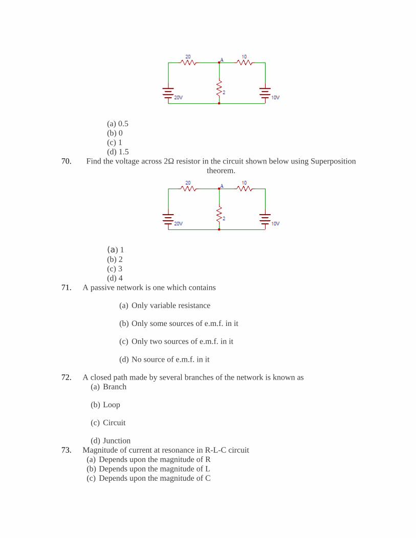
52. A conductor is said to have resistance of one ohm if a potential difference of onevolt across its terminals causes a current of X ampere to flow through it. What willbe the value of X?
(a) 4(b) 2(c) 3(d) 1
53. Resistance depends on the .……………..the conductor.(a) Temperature(b) Length(c) both(d) none
54. A basic network element which supplies power to the networks.(a) Source(b) Resistor (c) Diode(d) none of these
55. Every circuit is a network, but all networks are not ………………(a) Circuits(b) Resistor(c) Capacitor (d) inductor.
56. Find the equivalent resistance at node A in the delta connected circuit shown in thefigure below.

(a) 1(b) 2(c) 3(d) 4
57. Find the equivalent resistance between node 1 and node 3 in the star connectedcircuit shown below.
(a) 30(b) 31(c) 32(d) 33
58. KVL is based on the law of conservation of ………………(a) Energy(b) Momentum(c) Charge(d) Mass
59. Potential difference in electrical terminology is known as?(a) Voltage(b) Current(c) Resistance(d) Conductance
60. The circuit in which current has a complete path to flow is called …………….Circuit.
(a) short (b) open(c) closed(d) open loop
61. If the voltage-current characteristics is a straight line through the origin, then theelement is said to be………
(a) Linear element(b) Non-linear element(c) Unilateral element

(d) Bilateral element62. If the resistances 1Ω, 2Ω, 3Ω, 4Ω are parallel, then the equivalent resistance is?
(a) 0.46Ω(b) 0.48Ω(c) 0.5Ω(d) 0.52Ω
63. If the resistances 3Ω, 5Ω, 7Ω, 9Ω are in series, then their equivalent resistance(Ω)is?
(a) 9(b) 20(c) 24(d) 32
64. The current law represents a mathematical statement of fact that ___________(a) voltage cannot accumulate at node(b) charge cannot accumulate at node(c) charge at the node is infinite(d) none of the mentioned
65. Determine the current if a 20 coulomb charge passes a point in 0.25 seconds.(a) 10 A(b) 20 A(c) 2 A(d) 80 A
66. In Superposition theorem, while considering a source, all other voltage sourcesare…
(a) open circuited(b) short circuit(c) change its position(d) removed from the circuit
67. In Superposition theorem, while considering a source, all other current sources are?(a) short circuited(b) change its position(c) open circuited(d) removed from the circuit
68. Find the voltage across 2Ω resistor due to 20V source in the circuit shown below.
(a) 1(b) 1.5(c) 2(d) 2.5
69. Find the voltage across 2Ω resistor due to 20V source in the following circuit.
(a) 0.5(b) 0(c) 1(d) 1.5
70. Find the voltage across 2Ω resistor in the circuit shown below using Superpositiontheorem.
(a) 1(b) 2(c) 3(d) 4
71. A passive network is one which contains
(a) Only variable resistance
(b) Only some sources of e.m.f. in it
(c) Only two sources of e.m.f. in it
(d) No source of e.m.f. in it
72. A closed path made by several branches of the network is known as(a) Branch
(b) Loop
(c) Circuit
(d) Junction73. Magnitude of current at resonance in R-L-C circuit
(a) Depends upon the magnitude of R(b) Depends upon the magnitude of L(c) Depends upon the magnitude of C

(d) Depends upon the magnitude of R, Land C74. The safest value of current the human body can carry for more than 3 second is
(a) 4 mA(b) 9 mA(c) 15 mA(d) 25 mA
75. The purpose of a parallel circuit resonance is to magnify(a) Current(b) Voltage(c) Power(d) Frequency
76. Color coding is generally used to measure the value of a(a) Resistance (b) Capacitance(c) Inductance(d) None
77. Which of the following refers to a parallel circuit?(a) The current through each element is sam(b) The voltage across element is in proportion to it's resistance value(c) The equivalent resistance is greater than any one of the resistor(d) The current through any one element is less than the source current
78. The frequency of domestic power supply in India is(a) 200 Hz(b) 100 Hz(c) 60 Hz(a) 50 Hz
79. A heater is rated as 230 V, 10 kW, A.C. The value 230 V refers to(a) Average voltage(b) r.m.s. voltage(c) Peak voltage(d) None of the above
80. Which of the following statements pertains to resistors only?(a) Can dissipate considerable amount of power(b) Can act as energy storage devices(c) Connecting them in parallel increases the total value(d) Oppose sudden changes in voltage
81. Inductance affects the direct current flow
(a) Only at the time of turning off(b) Only at the time of turning on(c) At the time of turning on and off(d) At all the time of operation
82. A transformer cannot work on the DC supply because ……..__________________(a) There is no need to change the DC voltage(b) A DC circuit has more losses(c) Faraday’s laws of electromagnetic induction are not valid since the rate of
change of flux is zero(d) Cannot be determined
83. Identify the correct statement relating to the ideal transformer.(a) no losses and magnetic leakage(b) interleaved primary and secondary windings(c) a common core for its primary and secondary windings(d) core of stainless steel and winding of pure copper metal
84. Which of the following statement regarding an ideal single-phase transformer is incorrect? Transformer is having a turn ratio of 1: 2 and drawing a current of 10 A from 200 V AC supply is incorrect?
(a) It’s a step-up transformer(b) Its secondary voltage is 400 V(c) Its rating is 2 kVA(d) Its secondary current is 20 A
85. Ideal transformer core has permeability equal to _____(a) Zero(b) Non-zero finite(c) Negative(d) Infinite
86. Turns ratio of the transformer is directly proportional to ____________(a) Resistance ratio(b) Currents ratio(c) Voltage ratio(d) Not proportional to any terms
87. For transformer given, turns ratio is equal to ‘a’, what will be the impedance of primary with respect to secondary?
(a) a2 times the secondary impedance(b) ‘a’ times secondary impedance(c) secondary impedance/a(d) secondary impedance/a2
88. 89. Power transformed in the ideal transformer with turns ratio ‘a’ is _______(a) a2 times primary(b) ‘a’ times primary(c) primary power/ a2
(d) primary power90. For a transformer with primary turns 100, secondary turns 400, if 200 V is applied at
primary we will get ___________(a) 80 V at secondary(b) 800 V at secondary(c) 1600 V at secondary(d) 3200 V at secondary
91. For a transformer with primary turns 400, secondary turns 100, if 20A current is flowing through primary, we will get ___________
(a) 80A at secondary(b) 5A at secondary(c) 800A at secondary
(d) 40A at secondary92. Transformers windings are generally made of __________
(a) Steel(b) Iron(c) Copper(d) Steel iron alloy
93. Transformer core is designed to reduce ______________(a) Hysteresis loss(b) Eddy current loss(c) Hysteresis loss and Eddy current loss(d) Cannot be determined
94. Function of transformer is to……… _________________(a) Convert AC to DC(b) Convert DC to AC(c) Step down or up the DC voltages and currents(d) Step down or up the AC voltages and currents
95. The part of a transformer which is visible from outside _______________(a) Bushings(b) Core(c) Primary winding(d) Secondary winding
96. Network in electronics or electrical is a collection of ………_________.(a) Interconnected components(b) Alternately connected circuits(c) Disconnected devices(d) Disconnected components
97. An electric network in which current and voltage values are identified is called _______ process.
(a) Network analysis(b) Network bisection(c) Networking(d) None of the above
98. The flow of current through 2 or more input/output terminals of an electrical or electronic device is called………….
(a) Component(b) Node(c) Circuit(d) Mesh
99. A point where multiple component terminals meet is called ………_.(a) Component(b) Node(c) Circuit(d) Mesh
100. A conductor has ……… amount of resistance when considered as a node.(a) 0(b) 0.5
(c) 100(d) Infinite
101. In a network, source is connected on …………………… port.(a) Input(b) Output(c) Both ‘a’ and ‘b’(d) Not connected
102. Capacitance of 2 plates is expressed in terms of ………..(a) Ohms(b) Micro Farads(c) Henry(d) Mega Ohms
103. Inductance of a material is expressed in terms of …………….(a) Ohms(b) Farads(c) Henry(d) Columb’s
104. A procedure to simplify a network can be done by…………..the number of components.
(a) Reducing(b) Multiplying(c) Adding(d) None of the above
105. ………..in a network are replaced with other network components which provide same effect same effect.
(a) Physical components(b) Resistor(c) Impedance(d) All the above
106. …………….are used while solving network circuits.(a) Methods(b) Theorems(c) Logics(d) Both a and b
107. Impedance in network circuits is represented as …………. .
(a) R (b) L (c) Z (d) X
108. Ohms law was developed by ….(a) Georg ohm(b) John ohm(c) Henry ohm(d) Richard Ohm
109. The theorem used to transform a current type generator into a resistor is….(a) Nortons theorem(b) Kirchoff’s law
(c) Thevenin's theorem(d) Tellegen's theorem
110. Kirchhoff law has ………. number of additional theorems.(a) 2(b) 3(c) 4(d) 5
111. ……………. is expressed as the inverse of impedance.(a) Resistance(b) Admittance(c) Reactance(d) Capacitance
112. Resistance in Thevenin's networking theorem is calculated using by ……… type source type short-circuited source.
(a) Voltage(b) Current(c) Both a and b(d) None of the above
113. ………….theorem in networking defines that summing network elements are represented as single parallel resistors and current source.
(a) Tellegen's(b) Ohms(c) Thevenin's(d) Norton’s
114. Source conversion converts ……………. source to ……………… source.(a) Current to voltage(b) Voltage to current(c) Current to current(d) Both a and b
115. Star configuration used in networking circuits is also called as …… configuration.(a) Pi(b) Triangle(c) Rectangle(d) None of the above
116. Delta configuration used in networking circuits is also called ………configuration.(a) Pi(b) Triangle(c) Rectangle(d) None of the above
117. What is the 1st step of mesh analysis?(a) Each closed type loop is assigned a loop current(b) Kirchhoff's 2nd law is applied for each loop(c) Solve the equation to get loop current value(d) Both a and b
118. Which of the following is 1st step of nodal analysis?(a) Each node is assigned with arbitrary voltage
(b) Current in every branch is calculated(c) Kirchhoff 1st law at every node is applied(d) All the above
119. If a circuit operates with a constant current or voltage source, then the circuit is called a ………… circuit.
(a) AC circuit(b) DC circuit(c) ADC circuit(d) DAC circuit
120. Star configuration has ………..number of ports.(a) 2(b) 3(c) 4(d) Multiple
121. Delta network has ………… number of nodes.(a) 1(b) 2(c) 3(d) 4
122. Kirchhoff's 1st law is also called………….(a) Kirchhoff junction rule(b) Kirchhoff node rule(c) Kirchhoff point rule(d) All the above
123. Kirchhoff's 2nd law is also called as …………...(a) Kirchhoff voltage law(b) Kirchhoff current law(c) Kirchhoff resistance law(d) Both a and b
124. Which of the following is the disadvantage of Kirchhoff's laws?(a) Assumes zero magnetic fluctuation in closed type loop(b) Presence of electric field and electromotive force breaks the rule due
to change in magnetic flux(c) Both a and b(d) Electric field is 0
125. Norton's theorem is applied to the networks with …………..(a) Current source(b) Voltage source(c) Linear time invariant(d) All the above
126. Norton's theorem deals with …………… circuit theory.(a) AC(b) DC(c) ADC(d) DAC
127. Thevenin's theorem is applicable for …………. resistive circuits.

(a) AC(b) DC(c) ADC(d) DAC
128. A transformer is a ……………. device.(a) Static(b) Dynamic(c) Static and Dynamic(d) None of the above
129. The smallest set of variables that determines the state of the system are known as ….(a) State(b) State variables(c) State vector(d) None of the above
130. The argument of the complex number (-1+j) is……(a) 135(b) -45(c) 45(d) -135
131. The difference of two conjugate numbers results in(a) a complex number(b) in-phase component only(c) quadrature component only(d) none of the above
132. x+j y is called (a) An exponential number(b) An odd number(c) An even number(d) A complex number
133. The operator ‘j’ is equal to….(a) -1(b) +1(c) √−1(d) x
134. The physical size of a resistor determines…..(a) The voltage rating(b) The current rating(c) The power rating(d) The temperature rating
135. A 15 Ω resistor, an inductor with 8 Ω inductive reactance, and a capacitor with 12 Ωcapacitive reactance are in parallel across an ac voltage source. The circuit impedance is
(a) 12.7 Ω(b) 127 Ω(c) 4,436 Ω(d) 6,174 Ω

136. If the value of C in a series RLC circuit is decreased, the resonant frequency(a) Is not affected(b) Increases(c) Is reduced to zero(d) Decreases
137. A 24 Ω resistor, an inductor with a reactance of 120 Ω, and a capacitor with a reactance of 120 Ω are in series across a 60 V source. The circuit is at resonance. The voltage across the inductor is
(a) 60 V(b) 660 V(c) 30 V(d) 300 V
138. Q of the circuit stands for _...................factor.(a) Quality(b) Magnification(c) Tuning(d) Both a & b
139. ………_ resonant circuit works as a resistive circuit on a resonant frequency.(a) Series(b) Parallel(c) both a & b(d) none of the above
140. Quality factor (Q) of a circuit is also known as ………..(a) Figure of Merit(b) Series connector(c) Parallel connector(d) None of the above
141. The opposite of admittance is …………….(a) Resistance(b) Conductance(c) Impedance(d) inductance
142. It is necessarily to find ………… of current to solve the circuit according to the Kirchhoff’s Laws .
(a) Value(b) Direction(c) Symbol(d) speed
143. The circuits of star, delta star conversion, Thevenin theorem, Norton theorem etc. can be solved through the method of _______.
(a) node voltage method(b) loop voltage method(c) equivalent method(d) Both a & b
144. Laplace transformation is based on …….(a) Integral formula
(b) Differential formula (c) Both ‘a’ and ‘b’(d) None of the above
145. Laplace transforms of the function e−2t is….(a) 1/2s(b) (s + 2)(c) 1/(s+2)(d) 2s
146. The integral of a step function is……….(a) A ramp function(b) An impulse function(c) Modified ramp function(d) A sinusoidal function
147. Laplace transforms of tn u(t) is
(a)n!
sn
(b)n!
sn−1
(c)(n−1)!
sn−1
(d)n !
sn+1
148.The final value of the function I(s)=
s+6s (s+3)
is….
(a) 0(b) 1(c) 2(d) 3
149. Maximum power in terms of the Thevenin’s voltage and load resistance …..a) (VTh) 2 /4RL
b) (VTh) 2 *4RL
c) (VTh) 2 +4RL
d) 4RL/ (VTh) 2
150. In AC networks, maximum power is delivered when __________a) ZL*ZS*=0b) ZL+ZS*=1c) ZL=-ZS*d) ZL=ZS*

Group-B
151. Identify the process in which an electron escapes from the metal surface.(a) Electron emission(b) Electron displacement(c) Electron transgression(d) Electron movement
152. How many types of electron emissions exist?
(a) 2(b) 3(c) 4(d) 1
153. How does the intensity affect the photoelectric current?(a) As intensity increases, the photoelectric current increases(b) As the intensity increases, the photoelectric current decreases(c) As the intensity decreases, the photoelectric current becomes twice(d) No effect
154. The photoelectric emission could be explained by the ____________(a) Wave nature of light(b) Particle nature of light(c) Dual nature of light(d) Quantum nature
155. What is the effect of intensity on the stopping potential?a) As intensity increases, stopping potential increases linearlyb) As intensity increases, stopping potential decreases linearlyc) As intensity decreases, stopping potential increases exponentiallyd) No effect
156. Work function of metals is generally measured in
a) Joulesb) electron-voltc) watt-hourd) watt
157. At room temperature, the electron cannot escape metal surface due toa) Attractive forces of nucleusb) Repulsive forces of electrons
c) Repulsive forces of nucleusd) Pulling force of protons
158. The control grid of Triode is used to control the __________________.(a) Flow of Electrons(b) Flow of Holes(c) Flow of Electrons & Holes(d) All are correct
159. When anode voltages are increased then space charge becomes ___________.
(a) Eliminate(b) Decrease(c) Increase(d) Maintain
160. The relation between changing of Plate voltage and Grid voltage is called ___________.(a) Amplification Factor(b) Plate Resistance(c) Mutual Conductance(d) Saturation
161. When Plate voltage of the triode increases, the plate current becomes ___________.(a) Decreased(b) Increased(c) Same(d) Stop
162. A vacuum tube is also known as electronic valve because(a) it conducts only in one direction(b) electrons are enclosed in evacuated envelope(c) it carries electrons(d) it is an electronic device
163. A vacuum diode can be used as ___________.(a) Amplifier(b) Sound Detector(c) Oscillator(d) Rectifier
164. The forbidden band in silicon at 00 K is

(a) 1.1 eV(b) 0.785 eV(c) 1.5 eV(d).2.0 eV
165. Intrinsic semiconductors are those (a) Which are made of semiconductor material in its purest form (b) Which have zero energy gap (c) Which have more electrons than holes (d) Which are available locally
166. Intrinsic semiconductor at room temperature will have, ___________ available for conduction
(a) Electrons(b) Holes(c) Both electrons and holes(d) None of the above
167. The energy gap is much more in silicon than in germanium because(a) It has less number of electrons(b) It has high atomic mass number(c) Its crystal has much stronger bonds called ionic bonds(d) Its valence electrons are more tightly bound to their parent nuclei
168. A Semiconductor has___________ temperature coefficient of resistance.(a) negative(b) Positive(c) Zero(d) None of the above
169. A semiconductor generally has ___________ valence electrons(a) 2(b) 3(c) 4(d) 6
170. A doped semiconductor is also known as(a) Intrinsic semiconductor(b)Extrinsic semiconductor
(c)Diffused semiconductor(d) None of the above
171. Addition of pentavalent impurity to semiconductors creates many______(a) Free Electrons(b) Holes(c) Valence electrons(d) Bound electrons
172. A pentavalent impurity has________(a) 3 Valence electrons(b) 6 Valence electrons(c) 5 Valence electrons(d) 4 Valence electrons
173. A trivalent impurity has________(a) 3 Valence electrons(b) 6 Valence electrons(c) 5 Valence electrons(d) 4 Valence electrons
174. As the temperature of a semiconductor increases its(a) Conductivity increases(b)Resistivity increases(c)Atomic number decreases(d)Temperature co-efficient becomes zero
175. The conduction band(a) Is always above the forbidden energy level(b) Is the region of free electrons(c) Concentrates holes for the flow of current(d) Is a range of energies corresponding to the energies of the free electrons
176. The battery connections required to forward bias PN junction are(a)+ve terminal to p and -ve terminal to n(b)-ve terminal to p and +ve terminal to n(c)-ve terminal to p and -ve terminal to n(d) None of the above
177. The forbidden band in germanium at 00K is(a) 0.03 eV
(b) 0.785 eV(c) 1.5 eV(d).2.0 eV
178. The atomic number of germanium is.......(a) 4(b) 8(c) 16(d) 32
179. _________ is used to describe the static V/I characteristic of a junction diode(a) Bolzmann diode equation(b) Richardson-Dushman equation(c) Child's Three half-power law(d) Einstein's photoelectric equation
180. For a germanium P-N junction, the barrier potential is nearly_________(a) 0.3 V(b) 3.5 V(c) 3 V(d) Zero
181. A reversed biased PN Junction has_______(a) Very narrow depletion layer(b) Almost no current(c) Very low resistance(d) Large current flow
182. A PN Junction, acts as a _________(a)Unidirectional switch
(b) Bidirectional switch(c) Controlled switch(d) None of the above
183. A reverse biased PN junction has a resistance________(a) Of the order of Ω(b) Of the order of KΩ(c) Of the order of MΩ(d) None of the above
184. With forward bias to a PN junction the width of the depletion layer__________(a) Decreases

(b) Increases(c) Remains the same(d) None of the above
185. The leakage current in a PN junction is of the order of______(a) A(b) mA(c) kA(d) μA
186. Zener diodes are also known as(a) Voltage regulators(b) Forward bias diode(c) Breakdown diode(d) None of the mentioned
187. The zener diode is heavily doped because______(a) to have low breakdown voltage(b) to have high breakdown voltage(c) to have high current variations(d) to maintain perfect quiescent point
188. BJT stands for __________(a) Bi-Junction Transfer(b) Blue Junction Transistor(c) Bipolar Junction Transistor(d) Base Junction Transistor
189. A transistor has ______(a) one pn junction(b) two pn junctions(c) three pn junctions(d) four pn junctions
190. The base of a transistor is ______ doped(a) heavily(b) moderately(c) lightly(d) none of the above
191, A transistor is a ______ operated device
(a) current(b) voltage(c) both voltage and current(d) none of the above
192. The element that has the biggest size in a transistor is ______(a) collector(b) base(c) emitter(d) collector-base-junction
193. The collector of a transistor is ______ doped(a) heavily(b) moderately(c) lightly(d) none of the above
194. The emitter of a transistor is ______ doped(a) heavily(b) moderately(c) lightly(d) none of the above
195. The value of α of a transistor is ______ (a)more than 1
(b) less than 1(c) 1(d) none of the above
196. A JFET is also called ______ transistor(a) unipolar(b) bipolar(c) unijunction(d) none of the above
197. FETs are preferred to BJTs at high frequencies because they are(a) Less noisy(b) Capable of handling highest frequencies(c) Easy to fabricate(d) All of the above
198. The most commonly used transistor arrangement is ______ arrangement(a) common emitter(b) common base(c) common collector(d) none of the above
199. How many terminals are there in a unijunction transistor?(a) 1(b) 2(c) 3(d) 4
200. A UJT has ______(a) Two pn junctions(b) One pn junction(c)Three pn junctions(d)None of the above
201. What do you mean by transistor? (a) a semiconductor device (b) current(c) voltage (d) None of these
202. In a transistor, signal is transferred from a ___________ circuit. (a) high resistance to low resistance (b) low resistance to high resistance (c) high resistance to high resistance(d) low resistance to low resistance
203. In npn transistor, free electrons are the ____. (a) equal charge carriers(b) majority charge carriers (c) minority charge carriers (d) None of the above
204. The output impedance of a transistor is ___________. (a) high (b) zero (c) very low

(d) low
205. The input impedance of a transistor is ___________. (a) high (b) zero (c) very low
(d) low
206. As the temperature of a transistor goes up, the base-emitter resistance ____. (a) decreases(b) Increases (c) remains the same
(d) None of the above207. The name transistor is derived from ___ that means the resistance is changed.
A. ten resistorB. transfer runC. transfer resistor
D. None of the above208. The emitter-base junction of a transistor is ___ Biased while the collector-base
junction is ___. A. Reverse, Forward B. Reverse, Reverse C. Forward, forward D. Forward, reverse
209. In a pnp transistor, the majority current carriers are …………. A. holes B. donor ions C. acceptor ions D. free electrons
210. A zener diode has _______ breakdown voltage.(a) Undefined(b Sharp(c) Zero(d) None of the above
211. The collector current in the transistor will
a) Increase if the temperature increasesb) Decrease if the temperature decreasesc) Not change with the temperature variationd) None of the above
212. In a npn transistor, the minority current carriers are …………. (a) holes
(b) donor ions (c) acceptor ions (d) free electrons
213. A series resistance is connected in the zener circuit to ________.(a) Properly reverse bias the zener(b) Protect the zener(c) Properly forward bias the zener(d) None of the above
214. Transistors are generally made from ____. (a) silicon (b) iron (c) copper` (d) None of the above
215. In a npn transistor, the majority current carriers are …………. (a) holes (b) donor ions(c) acceptor ions (d) free electrons
216. A zener diode is destroyed if it ________.(a) Is forward biased(b) Is reverse biased(c) Carries more than rated current(d) None of the above
217. In a pnp transistor, the minority current carriers are …………. A. holes B. donor ions C. acceptor ions D. free electrons
218. A zener diode is _______ device.(a) A non-linear(b) A linear(c) An amplifying(d) None of the above
219. A UJT exhibits negative resistance whena) Current is less than valley current(b)Current is less than peak current(c) Current is more than peak current but less than valley current(d) None of the above
220. When the reverse voltage increases, the junction capacitance
(a) Decreases(b) Stays the same(c) Increases(d) Has more bandwidth
221. The p-n junction behaves like a
a) diodeb) triodec) tetroded) pentode
222. In the n-p-n transistors under forward biased condition, p layer is extremely thin becausea) The material used for p-type semiconductor is very costlyb) The p-type semiconductor requires more energy to disturb the electrons in the valence bandc) 90% electrons can be collected at the collectord) 90% electrons can be controlled at the emitter
223. The conduction in JEFT is always by the
a) Majority carriersb) Minority carriersc) Holesd) Electrons
224. The Hall Coefficient for p-type semiconductors is
a) Negative onlyb) Positive onlyc) Either positive or negatived) Not applicable
225.The Hall Coefficient will be zero fora) Insulatorb) N-type semiconductorc) Conductord) P-type semiconductor
226. Fermi Level is the energy where the probability of a state occupied in conduction and valance band isa) 0.1b) 0.5
c) 1.0d) 0.33
227. The thickness of depletion region in semiconductor diode is of the order of
a) 1 × 10⁻⁴ micronb) 1 × 10⁻⁶ micronc) 1 micrond) 1 × 10⁻⁶ cm
228. Which of the following transistor configuration will give both current and voltage gain?a) Common emitterb) Common collectorc) Common cased) None of the above
229. Why n-p-n transistors are preferred over the p-n-p transistors?
a) N-p-n transistors have low heat dissipationb) N-p-n transistors are cheap and easily availablec) N-p-n transistors have high mobility of holesd) N-p-n transistors have higher mobility of electrons than holes in p-n-p transistors
230. What are unijunction transistors used for?a) Amplifying a circuitb) Circuit breakerc) Splitting deviced) On-Off switching device
231. Which type of material is the channel of a unijunction transistor made up of?a) PN typeb) It doesn’t affect the workingc) P typed) N type
232. What are the working regions of a unijunction transistor?a) Linear regionb) Negative Resistance regionc) Saturation regiond) Cut-off region
233. What are the terminals of a unijunction transistor?a) Collector, Base and Emitterb) Emitter, Base 1 and Base 2c) Gate, Drain and Source
d) Gate, Drain, Body and Source234. The gate of FET is analogous to......... of BJT
(a) Base (b) Substrate (c) Emitter (d) Collector
235. The FETs are also known as (a) Linear devices (b) Square root law devices (c) Cube law devices (d) Square law devices
236. Which of the following statement is true about FET?(a) It has high output impedance(b) It has high input impedance(c) It has low input impedance(d) It does not offer any resistance
237. Comparing the size of BJT and FET, choose the correct statement?a) BJT is larger than the FETb) BJT is smaller than the FETc) Both are of same sized) Depends on application
238. What is the main advantage of FET which makes it more useful in industrial applications?a) Voltage controlled operationb) Less costc) Small sized) Semiconductor device
239. What is the value of current when the gate to source voltage is less than the pinch off voltage?a) 1 Ab) 5 Ac) 100 Ad) 0
240. What is the value of drain current when gate to source voltage is equal to pinch off voltage?a) 0 Ab) 1 Ac) 2 Ad) Cannot be determined
241. To use FET as a voltage controlled resistor, in which region it should operate?

a) Ohmic regionb) cut offc) Saturationd) cut off and saturation
242. For an n-channel FET, What is the direction of current flow?a) Source to drainb) Drain to sourcec) Gate to sourced) Gate to drain
243. For a p-channel FET, What is the direction of current flow?a) Source to drainb) Drain to sourcec) Gate to sourced) Gate to drain
244. The pinch off voltage of JFET is 5v. What is its cut off voltage?a) 2.5Vb) 3Vc) 4Vd) 5V
245. The action of JFET in its equivalent circuit can be represented as which of the following?a) Current controlled current sourceb) Current controlled voltage sourcec) Voltage controlled current sourced) Voltage controlled Voltage source
246. Which of the following is used as the recombination agent by semiconductor device manufactures?a) Silverb) Goldc) Platinumd) Aluminium
247. What is the SI unit of electron diffusion constant?a) cm2/sb) m2/sc) m/sd) none
248. In diffusion, the particles flow from a region of _______ to region of ___________a) High, lowb) Low , high

c) High , mediumd) Low, medium
249. Which of the following parameter describes the best movement of the electrons inside a semiconductor?a) Velocity gradientb) Diffusionc) Mobilityd) Density gradient
250. Which of the following term isn’t a part of the total current density in a semiconductor?a) Temperatureb) µc) ed) E
251. What does dn/dx represent?a) Velocity gradientb) Volume gradientc) Density gradientd) None
252. A zener diode works on the principle of_________a) tunneling of charge carriers across the junctionb) thermionic emissionc) diffusion of charge carriers across the junctiond) hopping of charge carriers across the junction
253 When the voltage across the zener diode increases_________a) temperature remains constant and crystal ions vibrate with large amplitudesb) temperature increases and crystal ions vibrate with large amplitudesc) temperature remains constant and crystal ions vibrate with smaller amplitudesd) temperature decreases and crystal ions vibrate with large amplitudes
254. Avalanche breakdown in zener diode is ______a) electric current multiplication takes placeb) phenomenon of voltage multiplication takes placec) electrons are decelerated for a period of timed) sudden rise in voltage takes place.
255. Bridge rectifier is an alternative fora) Full wave rectifierb) Peak rectifierc) Half wave rectifierd) None of the mentioned
256. In a full wave rectifier, the current in each diode flows for (a) whole cycle of the input signal

(b) half cycle of the input signal(c) more than half cycle of the input signal (d) none of the above
257. In a full wave rectifier, if the input frequency is 50 Hz, then output frequency will be (a) 50 Hz (b) 75 Hz (c) 100 Hz (d) 200 Hz
258. In a center tap full wave rectifier, if Vm is the peak voltage between center tap and one end of the secondary, the maximum voltage coming across the reverse bias diode is (a)Vm (b) 2 Vm (c) Vm/2 (d) Vm/√2
259. The maximum efficiency of full wave rectification is (a) 40.6% (b) 100% (c) 81.2% (d) 85.6%
260. The maximum efficiency of half wave wave rectification is (a) 40.6% (b) 100% (c) 81.2% (d) 85.6%
261. The ripple factor of a bridge rectifier is (a) 0.482 (b) 0.812 (c) 1.11 (d) 1.21
262. The bridge rectifier is preferred to an ordinary two diode full wave rectifier because (a) it needs much smaller transformer for the same output (b) no center tap required(c) less PIV rating per diode (d) all the above
263. Early effect in BJT refers to (a) avalanche breakdown (b) thermal breakdown

(c) base narrowing (d) Zener breakdown
264. The leakage current ICBO flows in (a) The emitter, base and collector leads (b) The emitter and base leads (c) The emitter and collector leads (d) The base and collector leads.
265. The emitter of the transistor is generally doped the heaviest because it (a) has to dissipate maximum power(b) has to supply the charge carriers (c) is the first region of transistor (d) must possess low resistance
266. Which of the following transistor configuration circuit is much less temperature dependent (a) common base (b) common emitter (c) common collector (d) none of the above
267. The CE amplifier circuit are preferred over CB amplifier circuit because they have(a) lower amplification factor (b) larger amplification factor (c) high input resistance and low output resistance (d) none of these
268. The number of Grids in the Pentode are__________________.(a) 1(b) 2(c) 3(d) 4
269. A metal is heated inside Vacuum tube called_________________.(a) Cathode(b) anode(c) Emitter(d) a & c are correct
270. A Tube consists of three electrodes is called ___________.(a) Diode(b) Pentode(c) Triode(d) Tetrode
271. A Tube consists of five electrodes is called ___________.(a) Diode
(b) Pentode(c) Triode(d) Tetrode
272. The another name of plate is ____________.(a) Grid(b) Cathode(c) Anode(d) Atom
273. The potential applied on the control grid of triode is called _____________.
(a) Signal(b) Cathode Biasing(c) Grid Biasing(d) Plate Biasing
274. Which of the following represents the best definition for the diffusion length for holes?(a) Average distance which an electron is injected travels before recombining withan electron(b) Average distance which a hole is injected travels before recombining with an electron(c) Average distance which a hole is injected travels before recombining with a hole(d) Average distance which an electron is injected before recombining with a hole
275. The change in the carrier density is due to(a) Flow of incoming flux(b) Flow of outgoing flux(c) Difference of flow between incoming and outgoing flux(d) Difference of flow between incoming and outgoing flux plus generation and minus recombination
276. What does p/τ represent?a) holesb) timec) holes per second lostd) p per unit time
277. Identify the correct condition for a semiconductor to be electrically neutral.a) Nd+p=Na+nb) Nd-p=Na+nc) Nd+p=Na-nd) Nd-p=Na-n
278. What is the SI unit of conductivity?a) Ωm
b) (Ωm)-1
c) Ωd) m
279. Which of the following expressions doesn’t represent the correct formula for Driftcurrent density?(a) J=σE(b) J=qnµE(c) J=µEd) None
280. In a semiconductor which of the following carries can contribute to the current?a) Electronsb) Holesc) Bothd) None
281. The number of Grids in the Pentode are__________________.(a) 1(b) 2(c) 3(d) 4
282. Number of secondary electrons emitted per number of primary electrons depends on
a) Material of targetb) Frequency of primary electronsc) Intensityd) None of the above
283. In a diode, when there is saturation current, the plate resistance is(a) Zero(b) Infinite(c) Some finite quantity(d) Data is insufficient
284. For a given plate voltage the plate current in a triode is maximum when the potential of
a) The grid is positive and the plate is negativeb) The grid is positive and the plate is positivec) The grid is zero and the plate is positived) The grid is negative and the plate is positive
285. The amplification produced by a triode is due to the action ofa) Filamentb) Cathodec) Gridd) plate

286. In a triode amplifier, the value of maximum gain is equal toa) Half the amplification factorb) Amplification factorc) Twice the amplification factord) Infinity
287. What are the two principal electrodes in every tube?a) Plate and control gridb) Cathode and screen gridc) Plate and cathoded) Screen grid and control grid
288. For a given plate voltage, if negative potential on the control grid of triode is increased, the plate current
a) decreasesb) remains the samec) increasesd) becomes zero
289. A triode can be used asa) an amplifierb) an oscillatorc) a rectifierd) a regulator
290. Which generates the least noise in operation?a) Triode valveb) Tetrode valvec) Pentode valved) Octode valve
291. A vacuum tube will conduct only if its plate is ______________ with respect to the cathode.
a) positiveb) negativec) at zero potentiald) at infinite potential
292. The voltage gain by the triode depends ona) Filament voltageb) Plate voltagec) Plate resistanced) Plate current
293. Before ionisation, a gas- filled tube has a _____________ resistance.a) very highb) very small

c) smalld) zero
294. The peak inverse voltage of a diode is defined as the maximum allowablea) negative voltage across the load resistorb) negative voltage applied to plate with respect to cathodec) positive voltage to plate with respect to cathoded) positive voltage applied across the load resistor
295. What is the typical value of ac plate resistance for a triode?a) 1000 Ωb) 100 kΩc) 1000 kΩd) 10 Ω
296. The plate resistance of a tube is mainly due toa) space chargeb) electrodes of the tubec) vacuum in the tubed) gas in the tube
297. A vacuum diode acts as a rectifier because of its ___________ conduction.a) unidirectionalb) bidirectionalc) isotropicd) omnidirectional
298. Saturation in a tube is a condition where an increase in plate voltage will producea) a rise in electron emissionb) a decrease in electron emissionc) no appreciable change in plate currentd) an appreciable change in plate current
299. In a triode valvea) If the grid voltage is zero then plate current will be zerob) If the temperature of the filament is doubled, then the thermionic current
will also be doubled.c) If the temperature of the filament is doubled, then the thermionic current
will nearly be four timesd) At a definite grid voltage, the plate current varies with plate voltage
according to Ohm’s law300. When the temperature of either n-type or p-type increases, determine the movement
of the position of the Fermi energy level?(a) Towards up of energy gap(b) Towards down of energy gap(c) Towards centre of energy gap

(d) Towards out of page
Model Question B.Sc (Electronics) Part-1
Paper-2
Q1. A transistor has ___________a) one pn junctionb) two pn junctionsc) three pn junctionsd) four pn junctions
Q2. In a pnp transistor, the current carriers are ___________a) acceptor ionsb) donor ionsc) free electronsd) holes
Q3. In a transistor, collector current is controlled by ___________a) collector voltageb) base currentc) collector resistanced) all of the above
Q4. Which is the least doped region in a transistor?a) Either emitter or collectorb) Basec) Emitterd) Collector
Q5. A current ratio of IC/IE is usually less than one and is called ___________a) betab) thetac) alphad) omega
Q6. Thermal stability can be obtained by_________a) shifting operating pointb) increasing power supplyc) heat sinkd) decreasing current at collector
Q7. The arrow in the symbol of a transistor indicates the direction of ___________a) electron current in the emitterb) electron current in the collectorc) hole current in the emitterd) donor ion current
Q8. A NPN transistor conducts whena) Both collector and emitter are positive with respect to the baseb) Collector is positive and the emitter is negative with respect to the basec) Collector is positive and the emitter is at the same potential as the based) Both collector and emitter are negative with respect to the base

Q9. The most commonly used semiconductor in the manufacture of a transistor is ___________a) germaniumb) siliconc) carbond) none of the above
Q10. In a transistor ___________a) IC = IE + IB
b) IB = IC + IE
c) IE = IC – IB
d) IE = IC + IB
Q11. In amplifier circuit, biasing of transistor is necessary toa) Fix the value of current amplificationb) Establish suitable D.C working conditionsc) Ensure that transistor is saturatedd) Ensure that transistor is cut-off
Q12. In a transistor highly doped part isa) Emitterb) Basec) Collectord) None of the above
Q13. A heat sink is generally used with a transistor to ___________a) increase the forward currentb) decrease the forward currentc) compensate for excessive dopingd) prevent excessive temperature rise
Q14. Transistor biasing represents ___________Conditionsa) a.c.b) d.c.c) both a.c. and d.c.d) none of the above
Q15. Voltage-divider bias provides ___________a) an unstable Q pointb) a stable Q pointc) a Q point that easily varies with changes in the transistor’s current gaind) a Q point that is stable and easily varies with changes in the transistor’s current
gainQ16. The configuration in which input impedance of transistor amplifier is lowest is
a) Common baseb) Common collectorc) Common emitterd) None of above
Q17. A transistor may be used as a switching device or as a ___________a) fixed resistorb) tuning devicec) rectifierd) variable resistor
Q18. The value of α of a transistor is ___________a) more than 1b) less than 1c) 1d) none of the above

Q19. When transistors are used in digital circuits they usually operate in the ___________a) active regionb) breakdown regionc) saturation and cut-off regionsd) linear region
Q20. The phase difference between the output and input voltages of a CE amplifier is ___________
a) 180o
b) 0o
c) 90o
d) 270o
Q21. The relation between β and α is ___________a) β = 1 / (1 – α )b) β = (1 – α ) / αc) β = α / (1 – α )sd) β = α / (1 + α )
Q22. Hybrid means ___________a) Mixedb) Singlec) Uniqued) None of the above
Q23. The output stage of a multistage amplifier is also called ___________a) Mixer stageb) Power stagec) Detector staged) F stage
Q24. When negative voltage feedback is applied to an amplifier, its voltage gain ___________a) Is increasedb) Is reducedc) Remains the samed) None of the above
Q25. Which of the following relation is true about gate current?a) IG=ID+IS
b) ID=IG
c) IS= IG
d) IG=0Q26. Transistor biasing is done to keep ___________in the circuit
a) Proper direct currentb) Proper alternating currentc) The base current smalld) Collector current small
Q27. It is generally desired that a transistor should have ___________input impedancea) Lowb) Very lowc) Highd) Very high
Q28. There are ___________h parameters of a transistora) Twob) Fourc) Threed) None of the above

Q29. The base of a transistor is ___________dopeda) heavilyb) moderatelyc) lightlyd) none of the above
Q30. ___________coupling is generally employed in power amplifiersa) Transformerb) RCc) directd) Impedance
Q31. The value of negative feedback fraction is always ___________a) Less than 1b) More than 1c) Equal to 1d) None of the above
Q32. Which of the following equations gives the relation between ID and Vgs?a) ID=IDSS (1-Vgs/Vp)2
b) ID=IDSS (1-Vgs/Vp)1
c) ID=IDSS (1-Vgs/Vp)3
d) ID=IDSS (1-Vgs/Vp)4
Q33. Operating point represents ___________a) Values of IC and VCE when signal is appliedb) The magnitude of signalc) Zero signal values of IC and VCE
d) None of the aboveQ34. When an a.c. signal is applied to an amplifier, ,the operating point moves along
___________a) d.c. load lineb) a.c. load linec) both d.c. and a.c. load linesd) none of the above
Q35. A JFET has three terminals, namely ___________a) cathode, anode, gridb) emitter, base, collectorc) source, gate, draind) none of the above
Q36. The h parameter approach gives correct results for ___________a) Large signals onlyb) Small signals onlyc) Both small and large signalsd) None of the above
Q37. A class A power amplifier uses ___________a) Two transistorsb) Three transistorsc) One transistord) None of the above
Q38. A feedback circuit usually employs ___________networka) Resistiveb) Capacitivec) Inductived) None of the above

Q39. For a fixed bias circuit the drain current was 1mA, what is the value of source current?a) 0mAb) 1mAc) 2mAd) 3mA
Q40. Transistor biasing is generally provided by a ___________a) Biasing circuitb) Bias batteryc) Dioded) None of the above
Q41. The main disadvantage of the FET is itsa) Low input impedanceb) Low thermal stabilityc) High noised) Low gain-band width product
Q42. The channel of a JFET is between the ___________a) gate and drainb) drain and sourcec) gate and sourced) input and output
Q43. In the zero signal conditions, a transistor sees ___________loada) d.c.b) a.c.c) both d.c. and a.c.d) none of the above
Q44. A transistor behaves as a linear device for ___________a) Small signals onlyb) Large signals onlyc) Both small and large signalsd) None of the above
Q45. The maximum efficiency of resistance loaded class A power amplifier is ___________a) 5%b) 50%c) 30%d) 25%
Q46. Which of the following current equations is true?a) IG = IDb) IG = ISc) ID = ISd) IG = ID = IS
Q47. A JFET is also called ___________ transistora) unipolarb) bipolarc) unijunctiond) none of the above
Q48. The gain of an amplifier with feedback is known as ___________gaina) Resonantb) Open loopc) Closed loopd) None of the above
Q49. A FET differs from a bipolar transistor as it has

a) Negative resistanceb) Simpler fabricationc) High input impedanced) Any of the above
Q50. What will happen if values of Rs increase?a) Vgs Increasesb) Vgs Decreasesc) Vgs Remains the samed) Vgs=0
Q51. For proper operation of the transistor, its collector should have ___________a) Proper forward biasb) Proper reverse biasc) Very small sized) None of the above
Q52. The source terminal of a JEFT corresponds to ___________of a vacuum tubea) plateb) cathodec) gridd) none of the above
Q53. The input capacitor in an amplifier is the ___________capacitora) Couplingb) Bypassc) Leakaged) None of the above
Q54. The parameter hie stands for input impedance in ___________a) CB arrangement with output shortedb) CC arrangement with output shortedc) CE arrangement with output shortedd) None of the above
Q55. For an amplifier, the FET is operated ina) Avalanche breakdown regionb) Pinch-off regionc) VVR regiond) None of the above
Q56. The self-bias configuration eliminates the need for two dc supplies.a) Trueb) False
Q57. The maximum efficiency of transformer coupled class A power amplifier is ………………a) 30%b) 50%c) 80%d) 45%
Q58. The point of intersection of d.c. and a.c. load lines represents ___________a) Operating pointb) Current gainc) Voltage gaind) None of the above
Q59. When voltage feedback (negative) is applied to an amplifier, its input impedance ___________
a) Is decreased
b) Is increasedc) Remains the samed) None of the above
Q60. The pinch-off voltage in a JFET is analogous to ___________voltage in a vacuum tubea) anodeb) cathodec) grid cut offd) none of the above
Q61. If a transistor amplifier draws 2mA when input voltage is 10 V, then its input impedance is ___________
a) 20 kΩb) 2 kΩc) 10 kΩd) 5 kΩ
Q62. The hfe parameter is called ___________in CE arrangement with output shorteda) Voltage gainb) Current gainc) Input impedanced) None of the above
Q63. A JFET is a ___________driven devicea) currentb) voltagec) both current and voltaged) none of the above
Q64. Which of the following is (are) true of a self-bias configuration compared to a fixed-bias configuration?
a) One of the dc supplies is eliminated.b) A resistor RS is added.c) VGS is a function of the output current ID.d) All of the above
Q65. Class __________ power amplifier has the highest collector efficiencya) Cb) Ac) Bd) AB
Q66. The disadvantage of base resistor method of transistor biasing is that it ___________a) Is complicatedb) Is sensitive to changes in βc) Provides high stabilityd) None of the above
Q67. Negative feedback is employed in ___________a) Oscillatorsb) Rectifiersc) Amplifiersd) None of the above
Q68. The purpose of capacitors in a transistor amplifier is to ___________a) Protect the transistorb) Cool the transistorc) Couple or bypass a.c. componentd) Provide biasing
Q69. If the operating point changes, the h parameters of transistor ___________a) Also changeb) Do not changec) May or may not changed) None of the above
Q70. For the field-effect transistor, the relationship between the input and the output quantities is_______.
a) linearb) nonlinearc) 3rd degreed) None of the above
Q71. Power amplifiers handle ___________signals compare to voltage amplifiersa) Smallb) Very smallc) Larged) None of the above
Q72. The biasing circuit has a stability factor of 50. If due to temperature change, ICBO changesby 1 µA, then IC will change by ___________
a) 100 µAb) 25 µAc) 20 µAd) 50 µA
Q73. The voltage gain of an emitter follower is ___________a) Much less than 1b) Approximately equal to 1c) Greater than 1d) None of the above
Q74. In the d.c. equivalent circuit of a transistor amplifier, the capacitors are considered ___________
a) Shortb) Openc) Partially shortd) None of the above
Q75. The gate of a JFET is ___________biaseda) reverseb) forwardc) reverse as well as forwardd) none of the above
Q76. The values of h parameter of a transistor in CE arrangement are ___________arrangementa) The same as for CBb) The same as for CCc) Different from that in CBd) None of the above
Q77. The input controlling variable for an FET transistor is a _______ level.a) resistorb) currentc) voltaged) All of the above
Q78. In class A operation, the operating point is generally located ___________of the d.c. load line.
a) At cut off point
b) At the middlec) At saturation pointd) None of the above
Q79. The leakage current in a silicon transistor is about ___________the leakage current in a germanium transistor
a) One hundredthb) One tenthc) One thousandthd) One millionth
Q80. When a negative voltage feedback is applied to an amplifier, its bandwidth ___________a) Is increasedb) Is decreasedc) Remains the samed) Insufficient data
Q81. In a FET, there are ___________pn junctions at the sidesa) threeb) fourc) fived) two
Q82. If RC and RL represent the collector resistance and load resistance respectively in a single stage transistor amplifier, then a.c. load is ___________
a) RL + RC
b) RC || RL
c) RL – RC
d) RC
Q83. In order to determine hfe and hie parameters of a transistor, ___________ is an a.c. short-circuited
a) Inputb) Outputc) Input as well as outputd) None of the above
Q84. The coupling capacitors are _______ for the dc analysis and _____________ for the ac analysis.
a) open-circuit, low impedanceb) short-circuit, low impedancec) open-circuit, high impedanced) None of the above
Q85. A power amplifier has comparatively ___________ βa) Smallb) Largec) Very larged) None of the above
Q86. In a p-channel JFET, the charge carriers are ___________a) electronsb) holesc) both electrons and holesd) none of the above
Q87. The operating point is also called the ___________a) Cut off pointb) Quiescent pointc) Saturation point
d) None of the aboveQ88. The output impedance of an emitter follower is ___________
a) Highb) Very highc) Almost zerod) Low
Q89. An amplifier has a power gain of 100. Its db gain is ___________a) 10 dbb) 20 dbc) 40 dbd) None of the above
Q90. The purpose of emitter capacitor (i.e. capacitor across RE) is to ___________a) Avoid voltage gain dropb) Forward bias the emitterc) Reduce noise in the amplifierd) None of the above
Q91. In a fixed-bias configuration, the voltage level of VGS is equal to _______.a) VS
b) Vg
c) VGS(off)d) VP
Q92. If the zero signal dissipation of a transistor is 1W, then power rating of the transistor should be at least ___________
a) 5 Wb) 33 Wc) 75 Wd) 1 W
Q93. The current in a coupling circuit for high frequencies isa) Zerob) Maximumc) Minimumd) Average
Q94. A JFET has ___________power gaina) smallb) very highc) very smalld) none of the above
Q95. Emitter follower is a ___________circuita) Voltage feedbackb) Current feedbackc) Both voltage and current feedbackd) None of the above
Q96. If temperature changes, h parameters of a transistor ___________a) May or may not changeb) Do not changec) Also changed) None of the above
Q97. For proper amplification by a transistor circuit, the operating point should be located at the ___________of the d.c. load line
a) The end point
b) Middlec) The maximum current pointd) None of the above
Q98. If the input capacitor of a transistor amplifier is short-circuited, then ___________a) Transistor will be destroyedb) Biasing conditions will changec) Signal will not reach the based) None of the above
Q99. The level of VDS is typically between _____ % and _____ % of VDD.a) 0, 100b) 10, 90c) 25, 75d) None of the above
Q100.
Which of the following is (are) feedback?a) Voltage-seriesb) Voltage-shuntc) Current-seriesd) D. All of the above
Q101.
In CE arrangement, the value of input impedance is approximately equal to ___________a) hie
b) hoe
c) hre
d) None of the aboveQ102
.When a transistor is cut off___________
a) Maximum voltage appears across transistorb) Maximum current flowsc) Maximum voltage appears across loadd) None of the above
Q103.
The demerit of a collector to base bias is_________a) its need of high resistance valuesb) its dependence on βc) its independence on βd) the positive feedback produced by the base resistor
Q104.
The disadvantage of voltage divider bias is that it has _________a) High stability factorb) Low base currentc) Many resistorsd) None of the above
Q105.
Which of the following cases damage the transistor?a) when VCE is increased too farb) when VCE is decreased too farc) when VBE is increased too fard) when VBE is decreased too far
Q106.
A transistor converts _____________a) d.c. power into a.c. powerb) a.c. power into d.c. powerc) high resistance into low resistanced) none of the above
Q107.
In which of the following configuration does a MOSFET works as an amplifier?a) Common Source (CS)b) Common Gate (CG)

c) Common drain (CD)d) All of the mentioned
Q108.
At what phase shift is the magnitude of βA at its maximum in the Nyquist plot?a) 90°b) 180°c) 270°d) D. 0°
Q109.
How many h-parameters of a transistor are dimensionless?a) Fourb) Twoc) Threed) One
Q110.
At cut-off, the JFET channel is _________a) at its widest pointb) completely closed by the depletion regionc) extremely narrowd) reverse biased
Q111.
The size of a power transistor is made considerably large to ___________a) Provide easy handlingb) Dissipate heatc) Facilitate connectionsd) None of the above
Q112.
The gate voltage in a JFET at which drain current becomes zero is called ___________voltage
a) saturationb) pinch-offc) actived) cut-off
Q113.
The thermal runway is avoided in a collector to base bias because_________a) of its independence of βb) of the positive feedback produced by the base resistorc) of the negative feedback produced by the base resistord) of its dependence of β
Q114.
Thermal runaway occurs when ___________a) Collector is reverse biasedb) Transistor is not biasedc) Emitter is forward biasedd) Junction capacitance is high
Q115.
________configuration has low thermal stabilitya) CEb) CBc) CCd) All of the above
Q116.
For highest power gain, one would use _____________ configurationa) CCb) CBc) CEd) none of the above
Q117.
The two important advantages of a JFET are ___________a) high input impedance and square-law propertyb) inexpensive and high output impedance

c) low input impedance and high output impedanced) none of the above
Q118.
A common- Source amplifier is similar to which BJT amplifier?a) Common-emitter amplifierb) Common-collector amplifierc) Common-base amplifiera) emitter-follower amplifier
Q119.
Only the condition βA = _____ must be satisfied for self-sustained oscillations to result.a) 0b) –1c) 1d) D. None of the above
Q120.
Low efficiency of a power amplifier results in ___________a) Low forward biasb) Less battery consumptionc) More battery consumptiond) None of the above
Q121.
Which of the following points locates the quiescent point?a) (IC, VCB)b) (IE, VCE)c) (IE, VCB)d) (IC, VCE)
Q122.
__________ has the lowest noise-levela) triodeb) ordinary transistorc) tetroded) JFET
Q123.
An amplifier is stable if the absolute magnitude of βA is _______.a) infinityb) less than 1c) greater than 1d) D. None of the above
Q124.
When ther transistor is operated in cut-off and saturation mode, it acts like aa) Linear Amplifierb) Photodiodec) LEDd) Switch
Q125.
Which of the following devices has the highest input impedance?a) JFETa) MOSFETb) Crystal diodec) ordinary transistor
Q126.
Power amplifiers generally use transformer coupling because transformer permits __________
a) Cooling of the circuitb) Impedance matchingc) Distortion less outputd) Good frequency response
Q127.
A JFET has high input impedance because __________a) it is made of semiconductor materialb) input is reverse biased

c) of impurity atomsd) none of the above
Q128.
The dimensions of hie parameters are _______a) Mhob) Ohmc) Faradd) Ampere
Q129.
In a transistor amplifier circuit VCE = VCB + _________a) VBE
b) 2VBE
c) 5 VBE
d) None of the aboveQ130
.CC configuration is used for impedance matching because its _________
a) Input impedance is very highb) Input impedance is lowc) Output impedance is very lowd) None of the above
Q131.
In the design of a biasing circuit, the value of collector load RC is determined by ______________
a) VCE considerationb) VBE considerationc) IB considerationd) None of the above
Q132.
The input control parameter of a JFET is _________a) gate voltageb) source voltagec) drain voltaged) gate current
Q133.
In a common-source JFET amplifier, the output voltage is ____________a) 180o out of phase with the inputb) in phase with the inputc) 90o out of phase with the inputd) taken at the source
Q134.
For DC, the current in a coupling circuit isa) Zerob) Maximumc) Minimumd) Average
Q135.
Reducing all dc sources to zero is one of the steps in getting thea) DC equivalent circuitb) AC equivalent circuitc) Complete amplifier circuitd) Voltage divider biased circuit
Q136.
The output resistance is given by _________a) ∆VCE/∆IB
b) ∆VBE/∆IB
c) ∆VBE/∆IC
d) ∆VCE/∆IC
Q137.
The small amount of current which flows even when base current IB=0 is called_________a) IBEO

b) ICBO
c) ICEO
d) IC
Q138.
A FET has no interelectrode capacitance, its band width isa) Lowb) Highc) Infinityd) Zero
Q139.
The operation of a JFET involves a flow ofa) Minority carriersb) Majority carriersc) Recombination carriersd) Any of the above
Q140.
Thermal stability is dependent on thermal runaway which is_________a) an uncontrolled positive feedbackb) a controlled positive feedbackc) an uncontrolled negative feedbackd) a controlled negative feedback
Q141.
If biasing is not done in an amplifier circuit, it results in ______________?a) Decrease in the base currentb) Unfaithful amplificationc) Excessive collector biasd) None of the above
Q142.
When Si NPN transistor in inactive, the base to emitter voltage is equal toa) 0.6b) 0.4c) 1.4d) 0.88
Q143.
A P-N-P transistor hasa) Only acceptor ionsb) Only donor ionsc) Two P-regions and one N-regiond) Three P-N junction
Q144.
In a FETa) One junction is forward biased and the other reverse biasedb) Both junctions are reverse biasedc) Both junctions are forward biasedd) None of the above
Q145.
In which region a transistor acts as an open switch?a) cut off regionb) inverted regionc) active regiona) saturated region
Q146.
What is the DC characteristic used to prove that the transistor is indeed biased in saturationmode?
b) IC = βIB
c) IC > βIB
d) IC >> βIB
e) IC < βIB
Q147.
In saturation region, the depletion layer_________a) increases linearly with carrier concentration
b) decreases linearly with carrier concentrationc) increases by increasing the emitter currentd) decreases by decreasing the emitter voltage drop
Q148.
An active device is one which ___________a) Mechanically controls electron flowb) Electrically controls electron flowc) Pneumatically controls electron flowd) Automatically controls electron flow
Q149.
FET acts as constant current source ina) Ohmic regionb) Breakdown regionc) Pinch off regiond) Both (b) and (c)
Q150.
The preferred from of biasing a JFET amplifier is ..... biasa) Selfb) Drainc) Sourced) Gate
Q151.
Active devices can also be used as_________a) Amplifiersb) Choppersc) Convertersd) Inverters
Q152.
In which region a transistor acts as a closed switch?a) cut off regionb) inverted regionc) active regiond) saturated region
Q153.
Op-Amp is abbreviated as ________.a) Operational Amplifierb) Operand amplitudec) Operational amplituded) None of the above
Q154.
Op-Amp is a ______ type of amplifier.a) Currentb) Voltagec) Powerd) Resistance
Q155.
Op-Amp has ________ inputs.a) Singleb) Similarc) Zerod) Differential
Q156.
Op-Amp has ________ outputs.a) Singleb) Similarc) Multipled) Differential
Q157.
Op-Amp with positive feedback acts as ________.a) Oscillatorb) Amplifier
c) Rectifierd) Clipper
Q158.
Op-Amp is originated from ________ computers.a) Analogb) Digitalc) Both a and bd) None of the above
Q159.
Op-Amp performs ________ operations.a) Arithmeticb) Logicalc) Alphanumericd) Both a and b
Q160.
Find the output voltage of an ideal op-amp. If V1 and V2 are the two input voltagesa) VO= V1- V2
b) VO = A×( V1- V2)c) VO = A×( V1+ V2)d) VO = V1× V2
Q161.
Balancing type feedback is also called as _______.a) Positive type feedbackb) Negative type feedbackc) Both a and bd) None of the above
Q162.
CMRR parameter in an instrumentation amplifier stands for ________.a) Common mode rejection ratiob) Common medium rejection ratioc) Common mode ratio of referenced) None of the above
Q163.
What is the value of CMRR of an ideal instrumentation amplifier?a) 1b) 0c) Infinityd) 0.5
Q164.
Ideal op-amp has infinite voltage gain becausea) To control the output voltageb) To obtain finite output voltagec) To receive zero noise output voltaged) None of the mentioned
Q165.
Which factor determine the output voltage of an op-amp?a) Positive saturationb) Negative saturationc) Both positive and negative saturation voltaged) Supply voltage
Q166.
Which of the following is the disadvantage of Op-amp ?a) Are designed for low power operation onlyb) Not suitable for high outputc) Requires passive componentsd) All the above
Q167.
Ideal Op-amp has ________ input impedance.a) 0b) Infinitec) Negative

d) Positivee) Hint
Q168.
Ideal Op-amp has ________ input offset voltage.a) 0b) Infinitec) Negatived) Positive
Q169.
A differential type amplifier in an Op-amp provides which of the following characteristics?a) Rejection of CM signalb) High input type impedancec) Low noised) All the above
Q170.
Slew rate is expressed in terms of ________.a) Volts/ secondsb) Amperes/ secondsc) Secondsd) Both a and b
Q171.
Which of the following are the applications of an op-amp?a) Voltage followersb) Selective inversion circuitc) Current to voltage converterd) All the above
Q172.
Does the real Op-amp have finite gain?e) Yesf) Nog) May beh) Not always
Q173.
Power supply rejection ratio is also called as ________.a) Supply voltage rejection ratiob) Supply current rejection ratioc) Supply rejection ratiod) None of the above
Q174.
Which of the following electrical characteristics is not exhibited by an ideal op-amp?a) Infinite voltage gainb) Infinite bandwidthc) Infinite output resistanced) Infinite slew rate
Q175.
An ideal op-amp requires infinite bandwidth becausea) Signals can be amplified without attenuationb) Output common-mode noise voltage is zeroc) Output voltage occurs simultaneously with input voltage changesd) Output can drive infinite number of device
Q176.
Generally, an op-amp is a _________ stage amplifier.a) Singleb) Doublec) Multid) Zero
Q177.
Op-Amp is available in the form of ________ package.a) ICb) Kitc) Device

d) All the aboveQ178
.The Barkhausen criterion for an oscillator
a) Loop gain should be unityb) Loop gain should be less than unityc) The phase of a feedback signal with respect to input should be 0° or 360°d) Both A and C
Q179.
The following are the necessary requirements of an oscillatora) Amplitude stabilityb) Frequency stabilityc) Power stabilityd) Both A and B
Q180.
An oscillator differs from an amplifier because ita) Has more gainb) Requires no input signalc) Requires no d.c. supplyd) Always has the same input
Q181.
Which of the following oscillators are used for low frequency (LF) applicationsa) LC oscillatorsb) RC oscillatorsc) Both LC and RC Oscillatorsd) None
Q182.
The expression for frequency of oscillations of a RC phase shift oscillator isa) f = 1 / (2π√RC)b) f = 1 / (2π√R(C1 + C2))c) f = 1 / (2π RC√6)d) none of the above
Q183.
An oscillator produces __________ oscillationsa) Dampedb) Undampedc) Modulatedd) None of the above
Q184.
LC oscillators are used for produce a waveform with frequency ranging froma) 1MHz to 500 MHzb) 100 KHz to 500 MHzc) 1 KHz to 1 MHzd) 1MHz to 100 GHz
Q185.
In Phase Shift oscillator, the frequency determining elements are__________a) L and Cb) R, L and Cc) R and Cd) None of the above
Q186.
An oscillator employs ___________ feedbacka) Positiveb) Negativec) Neither positive nor negatived) Data insufficient
Q187.
In an LC transistor oscillator, the active device is _________a) LC tank circuitb) Biasing circuitc) Transistord) None of the above
Q188.
In an LC oscillator, the frequency of oscillator is _________ L or C.a) Proportional to square ofb) Directly proportional toc) Independent of the values ofd) Inversely proportional to square root of
Q189.
In a phase shift oscillator, we use _________ RC sectionsa) Twob) Threec) Fourd) None of the above
Q190.
For an oscillator to properly start, the gain around the feedback loop must initially bea) 1b) Greater than 1c) Less than 1d) Equal to attenuation of feedback circuit
Q191.
In Colpitt’s oscillator, feedback is obtained ____________a) By magnetic inductionb) By a tickler coilc) From the centre of split capacitorsd) None of the above
Q192.
In an LC oscillator, if the value of L is increased four times, the frequency of oscillations is___________.
a) Increased 2 timesb) Decreased 4 timesc) Increased 4 timesd) Decreased 2 times
Q193.
The oscillator that is mostly used for generating signals of frequency of few 'MHz' isa) Armstrong oscillatorb) Crystal oscillatorc) Wein bridge oscillatord) Colpitts oscillator
Q194.
What must be done to ensure that oscillation will not die out in RC phase shift oscillator?a) Gain of amplifier is kept greater than 29b) Gain of amplifier is kept greater than 1c) Gain of amplifier is kept less than 29d) Gain of amplifier is kept less than 1
Q195.
The gain of an ideal oscillator isa) Unityb) Zeroc) Infinityd) Slightly more than unity
Q196.
The oscillator circuit with only D.C power source can be producea) Sinusoidal wave onlyb) Saw tooth wave onlyc) Square wave onlyd) Any of the above
Q197.
Ultra high frequency oscillators work in the rangea) 10 Hz to 10 kHzb) 1 kHz to 20 kHzc) 20 kHz to 30 MHzd) Above 30 MHz

Q198.
The most suitable oscillator circuits for 1 MHz frequency isa) Hartely oscillatorb) Phase shift oscillatorc) Wein bridge oscillatord) None of the above
Q199.
Which of the following is the main advantage of using oscillators?a) Suitability for low voltagesb) High output voltagec) Constant frequency of oscillationsd) High frequency
Q200.
______ oscillator is the most stable oscillatora) Crystal controlledb) Weinbridgec) Colpittsd) Hartley
Q201.
___________ oscillator uses a tapped coil in the LC tuned circuita) Hartleyb) Armstrongc) Colpittsd) Pierce
Q202.
Hartley oscillator is commonly used in ___________a) Radio receiversb) Radio transmittersc) TV receiversd) None of the above
Q203.
A ________ is a pulse generator circuit.a) multivibratorb) frequency generatorc) amplifierd) rectifier
Q204.
What rectifier does?a) converting DC to ACb) converting AC to DC c) converting high DC to low DC d) none of these
Q205.
Maximum efficiency of Half Wave Rectifier is:a) 25%b) 41% c) 65%d) 85%
Q206.
How many types of multivibrators are?a) 2b) 4c) 5d) 3
Q207.
Voltage regulators requirea) Only line regulationb) Only load regulationc) A constant loadd) Load and line regulation
Q208 Maximum efficiency of Full Wave Rectifier is:

. a) 25%b) 41%c) 65%d) 81%
Q209.
The external triggering is not needed for the transition of state in thea) Bistable multivibratorb) Monostable multvibratorc) Astable multivibratord) (b) and (c) both
Q210.
Astable Multivibrator is ________ in both of the states.a) stableb) unstablec) free runningd) all are correct
Q211.
Ripple factor =_____a) Irms / Idc b) Irms – Idcc) Irms + Idcd) Irms * Idc
Q212.
Bistable multivibrator is ________ in any state.a) Stableb) Unstablec) Saturatedd) Independent
Q213.
Voltage regulators keep a constant …………output voltage when the input or load varies within limits.
a) DCb) ACc) Rippled) None of above
Q214.
When load varies __________ voltage regulation maintains constant output voltagea) Lineb) Loadc) Both a and bd) None of the above
Q215.
In which rectifier value of ripple factor is less?a) Buck converterb) Full wave rectifierc) Half wave rectifierd) None of above
Q216.
What is a square wave generator?a) Flip-flopb) Bi-stable multivibratorc) Astable multivibratord) Monostable multivibrator
Q217.
What is the duty cycle of the output of an astable multivibrator?a) 50%b) 100%c) 75%d) 55%
Q218 Ripple factor of Half Wave Rectifier is:
. a) 3.21b) 2.21c) 1.21d) 0.21
Q219.
How can the duty cycle be changed for an astable multivibrator?a) By adding another capacitor to the circuitb) By adding diodes to the circuitc) By adding an inductor to the circuitd) The duty cycle cannot be changed
Q220.
The monostable multivibrator is a circuit whose output has a) two stable state and one quasi-stable stateb) one stable state and two quasi-stable statec) one stable state and one quasi-stable stated) two stable state only
Q221.
Ripple factor of Full Wave Rectifier is:a) 0.483b) 0.383c) 0.283d) 0.83
Q222.
Which of these is not a type of monostable multivibrator?a) Schmitt trigger as a monostable multivibratorb) Emitter coupled monostable multivibratorc) Using an op-ampd) 555 Timer as a monostable multivibrator
Q223.
Bistable circuit is also known as ____________a) Latchb) Gatec) Flip-flopd) Bidirectional circuit
Q224.
Multivibrators are characterized by ____________a) Registersb) Capacitorsc) Transistorsd) All of the Mentioned
Q225.
Astable circuit acts as a/an ____________a) Amplifierb) Oscillatorc) Relaxation oscillatord) Multiplexer
Q226.
The _______ stores the electric charges.a) transformerb) capacitorc) resistord) none of these
Q227.
In an astable multivibrator, the amplifying elements are ____________a) FETb) JFETc) OP-AMPd) All of the Mentioned
Q228.
Monostable multivibrator can also be termed as ____________a) Full astable multivibrator
b) Half astable multivibratorc) Half bistable multivibratord) Full bistable multivibrator
Q229.
When input voltage varies __________ voltage regulation maintains the constant output voltage
a) Lineb) Loadc) Both a and bd) None of the above
Q230.
The output voltage of a regulated power supply is affected by which of the following factors
a) Input voltageb) Load currentc) Temperatured) All the above
Q231.
Bridge rectifier is an alternative fora) Full wave rectifierb) Peak rectifierc) Half wave rectifierd) None of the mentioned
Q232.
To overcome ripple in rectifies DC, one can usea) A capacitor in series with a the load resistanceb) A capacitor in parallel to the load resistancec) Both of the mentioned situations will workd) None of the mentioned situations will work
Q233.
More complex circuitry that performs the opposite function, that is converting DC to AC, is called
a) communicationb) inverterc) common-moded) D. isolated
Q234.
Half-wave rectification requires a _______ diode in a single-phase supplya) singleb) doublec) multid) None of above
Q235.
C-filters are suitable for ___________ load resistancesa) lowb) highc) alld) none of above
Q236.
L-filters are suitable for ___________ load resistancesa) lowb) highc) alld) none of above
Q237.
A capacitor filter or C filter can be used in a rectifier by connecting ita) in parallel with the loadb) in series with the loadc) in parallel with the supplyd) in series with the supply
Q238.
An inductor filter connected in series with a resistive load provides aa) smoothing of the output voltage waveformb) smoothing of the input voltage waveformc) smoothing of the output current waveformd) smoothing of the input current waveform
Q239.
An L filter is connected ________a) in seriesb) in parallelc) in both series and paralleld) none of the mentioned
Q240.
In a half-wave rectifier, thea) current & voltage both are bi-directionalb) current & voltage both are uni-directionalc) current is always uni-directional but the voltage can be bi-directional or uni-
directionald) current can be bi-directional or uni-directional but the voltage is always uni-
directionalQ241
.An astable multivibrator requires:
a. balanced time constantsb. a pair of matched transistorsc. no input signalb) dual J-K flip-flops
Q242.
What controls the output pulse width of a one shot?a) the clock frequencyb) the width of the clock pulsec) an RL time constantd) an RC time constant
Q243.
The RMS value of a half wave rectifier current is 10 A. Its value for full wave rectification would bea) 10 Ab) 14.14 Ac) 20/Pi Ad) 20 A
Q244.
For single phase supply frequency of 50 Hz, ripple frequency in half wave rectifier is (in Hz)
a) 25b) 50c) 100d) 200
Q245.
For single phase supply frequency of 50 Hz, ripple frequency in full wave rectifier is (in Hz)
a) 25b) 50c) 100d) 200
Q246.
In case of a C filter, the AC is not allowed to pass to the load bya) offering it high impedanceb) offering it low impedancec) short circuiting the AC componentd) open circuiting the AC component
Q247 When a capacitor charges:

. a) the voltage across the plates rises exponentiallyb) the circuit current falls exponentiallyc) the capacitor charges to the source voltage in 5×RC secondsd) all of the above
Q248.
Pulse stretching, time-delay, and pulse generation are all easily accomplished with which type of multivibrator circuit?
a. astableb. monostablec. multistabled. bistable
Q249.
Peak inverse voltage for a diode is thea) Voltage corresponding to rated maximum voltageb) Maximum voltage that can be applied across the diode in the conducting directionc) Maximum voltage that can be applied across the diode in the non-conducting
directiond) None of the above
Q250.
The current in a Zener diode is controlled bya) Zener diode resistanceb) Potential barrierc) Reverse bias voltaged) External circuits
Q251.
The diode which is preferred for D.C coupling isa) LEDb) Power diodec) Signal dioded) Zener diode
Q252.
In case of a C filter, if R (load resistance) is increaseda) ripple factor is reducedb) ripple factor is increasedc) ripple factor is not affectedd) increases noise in the circuit
Q253.
When voltage applied to a diode is more than PIV, it is likely to result ina) More distortion on output sideb) Poor regulationc) Conduction in both directiond) Breakdown at the junction
Q254.
Modulation is the phenomenon of___________a) superimposing the audio frequency signal over a carrier waveb) separating the audio frequency signal from the carrier wavec) separating carier wave from the modulated waved) any of 'a, 'b,c above
Q255.
Modulation is done in___________a) Transmitterb) Radio receiverc) Between transmitter and radio receiverd) None of the above
Q256.
A modulation index of 0.5 would be same ase) 0.5 of Modulation Depthf) 1/2% of Modulation Depthg) 5% of Modulation Depthh) 50% of Modulation Depth

Q257.
Aliasing refers toa) Sampling of signals less than at Nyquist rateb) Sampling of signals greater than at Nyquist ratec) Sampling of signals at Nyquist rated) d. None of the above
Q258.
Amplitude modulation ise) Change in amplitude of the carrier according to modulating signalf) Change in frequency of the carrier according to modulating signalg) Change in amplitude of the modulating signal according to carrier signalh) Change in amplitude of the carrier according to modulating signal frequency
Q259.
Demodulation is the__________e) process of changing of modulating wave as the carrier wavef) process of coupling modulated wave with modulating waveg) process of separating carrier wave from the modulated waveh) process of combining the message signal with carrier wave
Q260.
Which devices we use for AM demodulation________Diode detector
a) Transducer b) Both a and bc) None of these
Q261.
The amount of data transmitted for a given amount of time is calleda) Bandwidthb) Frequencyc) Noised) d. Signal power
Q262.
In a communication system, noise is most likely to affect the signal______e) at the transmitterf) in the transmission mediumg) in the formation sourceh) at the destination
Q263.
In an AM wave useful power is carrier by ___________a) Carrierb) Sidebandsc) Both sidebands and carrierd) None of the above
Q264.
Carrier waves are_________a) high frequency wavesb) low frequency wavesc) information signald) audio waves
Q265.
Amplitude modulation is used for broadcasting because______a) it is more noise immune than other modulation systemsb) compared with other systems, it requires less transmitting powerc) its circuitry is simpled) no other modulation systems can provide the necessary bandwidth for high fidelity
Q266.
In AM modulation the bandwidth(ω) is equal to:a) B = 2 ωm
b) b. B = (ωc + ωm) - (ωc - ωm)c) c. ωm
d) d. None of the aboveQ267 The ability of the receiver to select the wanted signals among the various incoming signals
. is termed asa) Sensitivityb) Selectivityc) Stabilityd) None of the above
Q268.
Super heterodyne receiversa) Have better sensitivityb) Have high selectivityc) Need extra circuitry for frequency conversiond) All of the above
Q269.
In frequency modulation_______a) frequency of the carrier remains constantb) carrier frequency varies in accordance with the modulating signal frequencyc) carrier frequency varies in accordance with the modulating signal amplituded) both 'a' and 'b'
Q270.
The ratio between the modulating signal voltage and the carrier voltage is called?a) Amplitude modulationb) Modulation frequencyc) Modulation indexd) Ratio of modulation
Q271.
Two forms of angular modulation are_______a) phase modulation and frequency modulationb) phase modulation and amplitude modulationc) frequency modulation and amplitude modulationd) any of above
Q272.
Super heterodyne receiversa) Have better sensitivityb) Have high selectivityc) Need extra circuitry for frequency conversioni) All of the above
Q273.
In amplitude modulation, the bandwidth is________e) twice the audio signal frequencyf) thrice the audio signal frequencyg) thrice the carrier wave frequencyh) twice the carrier wave frequency
Q274.
In A.M., the total modulation index should not exceed one or else_________e) the system will failf) distortion will result g) amplifier will be damagedh) either a or c
Q275.
Standard intermediate frequency used for AM receiver isa) 455 MHzb) 455 KHzc) 455 Hzd) None of the above
Q276.
The modulation index of an over modulated wave is___________a) 1b) <1c) 0d) >1
Q277 An SCR has _________ pn junctions

. a) Twob) Threec) Fourd) None of the above
Q278.
An SCR is a solid state equivalent of __________e) Triodef) Pentodeg) Gas-filled triodeh) Tetrode
Q279.
An SCR has _________ semiconductor layersa) Twob) Threec) Fourd) None of the above
Q280.
An SCR has three terminals viz _____,_____,_____a) Cathode, anode, gateb) Anode, cathode, gridc) Anode, cathode, draind) None of the above
Q281.
An SCR behaves as a ____________. switcha) Unidirectionalb) Bidirectionalc) Mechanicald) None of the above
Q282.
An SCR is sometimes called ____________a) Triacb) Diacc) Unijunction transistord) Thyristor
Q283.
In the normal operation of an SCR, anode is ____________ w.r.t. cathodea) At zero potentialb) Negativec) Positived) None of the above
Q284.
In normal operation of an SCR, gate is _______ w.r.t. cathodea) Positiveb) Negativec) At zero potentiald) None of the above
Q285.
An SCR combines the features of ___________
a) A rectifier and resistanceb) A rectifier and transistorc) A rectifier and capacitord) None of the above
Q286.
The control element of an SCR is _________a) Cathodeb) Anodec) Anode supplyd) Gate
Q287 The normal way to turn on a SCR is by __________
. a) Breakover voltageb) Appropriate anode currentc) Appropriate gate currentd) None of the above
Q288.
An SCR is turned off by _________a) Reducing anode voltage to zerob) Reducing gate voltage to zeroc) Reverse biasing the gated) None of the above
Q289.
An SCR is a ____________ triggered devicea) Voltageb) Currentc) Voltage as well as currentd) None of the above
Q290.
When an SCR is turned on, the voltage across it is about _________a) Zerob) 10 Vc) 100 Vd) 1 V
Q291.
An SCR is made of silicon and not germanium because silicon ___________a) is inexpensiveb) is mechanically strongc) has small leakage currentd) is tetravalent
Q292.
If firing angle in an SCR circuit is increased, the output ________a) Remains the sameb) Is increasedc) Is decreasedd) None of the above
Q293.
When SCR starts conducting, then ________ loses all controla) Gateb) Cathodec) Anoded) None of the above
Q294.
During the normal operation of an SCR the gate is __________a) Negative w.r.t. cathodeb) Positive w.r.t. cathodec) At zero potentiald) None of the above
Q295.
AC power in a load can be controlled by connecting______________a) Two SCRs in seriesb) Two SCRs in parallelc) Two SCRs in parallel oppositiond) None of the above
Q296.
An SCR can be used a) as static conductorb) for power controlc) for speed control of dc shunt motord) all of these
Q297.
With gate open, the maximum anode current at which SCR is turned off from ON condition is called

a) breakdown voltageb) peak reverse voltagec) holding currentd) latching current
Q298.
A single phase ac - dc converter is also known asa) rectifierb) inverterc) chopperd) regulator
Q299.
If the gate voltage of an SCR is removed, then thea) anode current decreasesb) anode current does not decrease at allc) anode current increasesd) cathode current increases
Q300.
In a silicon controlled rectifier, the load is connecteda) Across anodeb) In series with anodec) Across cathoded) In series with cathode