
MODEL 372XXC/373XXC VECTOR NETWORK ANALYZER MAINTENANCE MANUAL
222
P/N: 10410-00228 REVISION: D PRINTED: AUGUST 2004 COPYRIGHT 2004 ANRITSU CO. MODEL 372XXC/373XXC VECTOR NETWORK ANALYZER MAINTENANCE MANUAL 490 JARVIS DRIVE l MORGAN HILL, CA 95037-2809
Transcript of MODEL 372XXC/373XXC VECTOR NETWORK ANALYZER MAINTENANCE MANUAL

P/N: 10410-00228REVISION: D
PRINTED: AUGUST 2004COPYRIGHT 2004 ANRITSU CO.
MODEL372XXC/373XXC
VECTOR NETWORK ANALYZER
MAINTENANCE MANUAL
490 JARVIS DRIVE l MORGAN HILL, CA 95037-2809

WARRANTY
The Anritsu product(s) listed on the title page is (are) warranted against defects in materials andworkmanship for three years from the date of shipment.Anritsu’s obligation covers repairing or replacing products which prove to be defective during thewarranty period. Buyers shall prepay transportation charges for equipment returned to Anritsu forwarranty repairs. Obligation is limited to the original purchaser. Anritsu is not liable for consequen-tial damages.
LIMITATION OF WARRANTY
The foregoing warranty does not apply to Anritsu connectors that have failed due to normal wear.Also, the warranty does not apply to defects resulting from improper or inadequate maintenance bythe Buyer, unauthorized modification or misuse, or operation outside of the environmental specifica-tions of the product. No other warranty is expressed or implied, and the remedies provided hereinare the Buyer’s sole and exclusive remedies.
TRADEMARK ACKNOWLEDGEMENTS
V Connector and K Connector are registered trademarks of Anritsu Company.MS-DOS is a registered trademark of Microsoft Corporation.Acrobat and Acrobat Reader are registered trademarks of Adobe Systems Incorporated.
NOTICE
Anritsu Company has prepared this manual for use by Anritsu Company personnel and customersas a guide for the proper installation, operation and maintenance of Anritsu Company equipmentand computer programs. The drawings, specifications, and information contained herein are theproperty of Anritsu Company, and any unauthorized use or disclosure of these drawings, specifica-tions, and information is prohibited; they shall not be reproduced, copied, or used in whole or in part


Table of Contents, Narrative
Chapter 1—General Service InformationThis chapter provides a general description of Series 372XXC/373XXC Vector Network Analyzer sys-tems, system serial numbers, and frequency ranges. It explains the level of maintenance covered in thismanual and the service strategy used throughout this manual. It also contains static-sensitive compo-nent handling precautions and a list of recommended test equipment.
Chapter 2—Replaceable PartsThis chapter lists all replaceable subassemblies and components for all 372XXC/373XXC models. It ex-plains the Anritsu exchange assembly program and provides parts ordering information.
Chapter 3—Theory of OperationThis chapter provides descriptions of the functional operation of the major assemblies contained inSeries372XXC/373XXC Vector Network Analyzer systems. The operation of all major circuit blocks isdescribed so that the reader may better understand the function of each assembly as part of the overalloperation.
Chapter 4—Operational Performance TestsThis chapter contains procedures that provide a means of fully testing the 372XXC/373XXC VNA sys-tem for proper operation and signal stability. These tests are intended to be used as a periodic check ofthe operational functionality of the 372XXC/373XXC.
Chapter 5—System Performance VerificationThis chapter provides a detailed procedure for verifying that the 372XXC/373XXC is capable of makingaccurate S-parameter measurements.
Chapter 6—AdjustmentsThis chapter provides adjustment procedures for all models of Series 372XXC/373XXC Vector NetworkAnalyzer systems. These procedures are used after replacement or repair of one or more critical subas-semblies, or as indicated by the operational performance tests contained in Chapter 4.
Chapter 7—TroubleshootingThis chapter provides information for troubleshooting Series 372XXC/373XXC Vector Network Ana-lyzer systems. The troubleshooting procedures contained in this chapter support fault isolation down toa replaceable subassembly.
Chapter 8—Removal and Replacement ProceduresThis chapter describes how to gain access to all of the major assemblies and major parts for trouble-shooting and/or replacement.
372XXC/373XXC MM i

Appendix A—Error MessagesThis appendix contains a listing of the Error Codes/Messages. Also included is a description of the infor-mation fields that are part of the error messages.
Appendix B—Connector Care and HandlingThis appendix contains procedures and information needed to perform maintenance checks (includingpin-depth measurements) for the connectors on all Anritsu supplied Calibration/Verification Kit com-ponents, Through-cables, and other associated RF/microwave components.
Appendix C—Performance SpecificationsThis appendix contains a copy of the 37100C/37200C/37300C Series Vector Network Analyzers, Tech-nical Data Sheet, Anritsu part number 11410-00247. This datasheet provides performance specifica-tions for all models in the series.
Appendix D—ME7808A Broadband Measurement System MaintenanceThis appendix provides maintenance and verifications instructions for the ME7808A BroadbandMeasurement System. This maintenance and verification is performed independently of anywafer-probe station. Models 37397C and 37297C are completely interchangeable in this system, andseveral models of synthesizers may be used with this system.
Subject Index
ii 372XXC/373XXC MM
Table of Contents, Narrative (Continued)

Table of ContentsChapter 1 General Information
1-1 SCOPE OF MANUAL · · · · · · · · · · · · · · · · · · · · · · · · · · · · · · · · · 1-3
1-2 INTRODUCTION · · · · · · · · · · · · · · · · · · · · · · · · · · · · · · · · · · · 1-3
1-3 IDENTIFICATION NUMBER· · · · · · · · · · · · · · · · · · · · · · · · · · · · · 1-3
1-4 ONLINE MANUAL · · · · · · · · · · · · · · · · · · · · · · · · · · · · · · · · · · 1-3
1-5 SYSTEM DESCRIPTION · · · · · · · · · · · · · · · · · · · · · · · · · · · · · · · 1-4
1-6 RELATED MANUALS· · · · · · · · · · · · · · · · · · · · · · · · · · · · · · · · · 1-4
1-7 STANDARD OPTIONS · · · · · · · · · · · · · · · · · · · · · · · · · · · · · · · · 1-5
1-8 SERVICE STRATEGY· · · · · · · · · · · · · · · · · · · · · · · · · · · · · · · · · 1-5Functional Assembly Level Troubleshooting . . . . . . . . . . . . . . . . . . . 1-5Internal Hardware Adjustments and Calibrations. . . . . . . . . . . . . . . . 1-6Internal Service Log . . . . . . . . . . . . . . . . . . . . . . . . . . . . . . . . 1-6System Test/Certification . . . . . . . . . . . . . . . . . . . . . . . . . . . . . 1-7Servicing Specially Modified Instruments . . . . . . . . . . . . . . . . . . . . 1-7
1-9 SERVICE SUPPORT · · · · · · · · · · · · · · · · · · · · · · · · · · · · · · · · · 1-7Technical Support . . . . . . . . . . . . . . . . . . . . . . . . . . . . . . . . . 1-7Field Service Kits . . . . . . . . . . . . . . . . . . . . . . . . . . . . . . . . . 1-8Service Software . . . . . . . . . . . . . . . . . . . . . . . . . . . . . . . . . . 1-8Verification Kits . . . . . . . . . . . . . . . . . . . . . . . . . . . . . . . . . . 1-9Test Fixtures/Aids . . . . . . . . . . . . . . . . . . . . . . . . . . . . . . . . . 1-9Failed Assembly Exchange Program . . . . . . . . . . . . . . . . . . . . . . 1-10
1-10 PERFORMANCE SPECIFICATIONS · · · · · · · · · · · · · · · · · · · · · · · · 1-10
1-11 SERVICE CENTERS · · · · · · · · · · · · · · · · · · · · · · · · · · · · · · · · · 1-10
1-12 STATIC SENSITIVE COMPONENT HANDLING PROCEDURES · · · · · · · · 1-10
1-13 RECOMMENDED TEST EQUIPMENT · · · · · · · · · · · · · · · · · · · · · · 1-12
Chapter 2 Replaceable Parts2-1 INTRODUCTION · · · · · · · · · · · · · · · · · · · · · · · · · · · · · · · · · · · 2-3
2-2 EXCHANGE ASSEMBLY PROGRAM · · · · · · · · · · · · · · · · · · · · · · · · 2-3
2-3 REPLACEABLE SUBASSEMBLIES AND PARTS · · · · · · · · · · · · · · · · · 2-4
2-4 PARTS ORDERING INFORMATION · · · · · · · · · · · · · · · · · · · · · · · · 2-4
372XXC/373XXC MM iii

Chapter 3 Theory of Operation3-1 INTRODUCTION · · · · · · · · · · · · · · · · · · · · · · · · · · · · · · · · · · · 3-3
3-2 SYSTEM OVERVIEW · · · · · · · · · · · · · · · · · · · · · · · · · · · · · · · · · 3-3
3-3 ANALOG SUBSYSTEM ASSEMBLIES · · · · · · · · · · · · · · · · · · · · · · · 3-8Signal Source Module . . . . . . . . . . . . . . . . . . . . . . . . . . . . . . . 3-8Test Set Module . . . . . . . . . . . . . . . . . . . . . . . . . . . . . . . . . . 3-9A7 PCB 10 MHz Timebase . . . . . . . . . . . . . . . . . . . . . . . . . . . . 3-10Receiver Module . . . . . . . . . . . . . . . . . . . . . . . . . . . . . . . . . 3-11A8, Source Lock/Signal Separation and Control PCB . . . . . . . . . . . . . 3-12IF Section . . . . . . . . . . . . . . . . . . . . . . . . . . . . . . . . . . . . . 3-12A7 PCB, LO3 . . . . . . . . . . . . . . . . . . . . . . . . . . . . . . . . . . . 3-13A5 A/D Converter PCB. . . . . . . . . . . . . . . . . . . . . . . . . . . . . . 3-13
3-4 DIGITAL SUBSYSTEM ASSEMBLIES · · · · · · · · · · · · · · · · · · · · · · · 3-14A9 Main Processor PCB Assembly . . . . . . . . . . . . . . . . . . . . . . . 3-14A13 I/O Interface #1 PCB Assembly. . . . . . . . . . . . . . . . . . . . . . . 3-16A14 I/O Interface #2 PCB Assembly. . . . . . . . . . . . . . . . . . . . . . . 3-16A15 Graphics Processor PCB Assembly . . . . . . . . . . . . . . . . . . . . . 3-17A16 Hard Disk PCB Assembly. . . . . . . . . . . . . . . . . . . . . . . . . . 3-17Floppy Disk Drive Assembly. . . . . . . . . . . . . . . . . . . . . . . . . . . 3-17A24 VME Bus Terminator PCB . . . . . . . . . . . . . . . . . . . . . . . . . 3-17
3-5 MAIN CHASSIS ASSEMBLIES · · · · · · · · · · · · · · · · · · · · · · · · · · · 3-17A17 System Motherboard Assembly. . . . . . . . . . . . . . . . . . . . . . . 3-17Front Panel Assembly . . . . . . . . . . . . . . . . . . . . . . . . . . . . . . 3-18A18 Rear Panel Interface PCB. . . . . . . . . . . . . . . . . . . . . . . . . . 3-18Power Supply Module . . . . . . . . . . . . . . . . . . . . . . . . . . . . . . 3-19
Chapter 4 Operational Performance Tests4-1 INTRODUCTION · · · · · · · · · · · · · · · · · · · · · · · · · · · · · · · · · · · 4-3
4-2 CHECKING THE SERVICE LOG · · · · · · · · · · · · · · · · · · · · · · · · · · 4-4
4-3 SELF TEST · · · · · · · · · · · · · · · · · · · · · · · · · · · · · · · · · · · · · · 4-5
4-4 PERFORMANCE TESTS · · · · · · · · · · · · · · · · · · · · · · · · · · · · · · · 4-6Test Specifications . . . . . . . . . . . . . . . . . . . . . . . . . . . . . . . . . 4-6Required Equipment. . . . . . . . . . . . . . . . . . . . . . . . . . . . . . . . 4-7Additional Required Equipment . . . . . . . . . . . . . . . . . . . . . . . . . 4-7Installation and Launching the Test Program . . . . . . . . . . . . . . . . . . 4-7Running the Tests . . . . . . . . . . . . . . . . . . . . . . . . . . . . . . . . . 4-9Description of Tests . . . . . . . . . . . . . . . . . . . . . . . . . . . . . . . . 4-9
iv 372XXC/373XXC MM
Table of Contents (Continued)

Chapter 5 System Performance Verification5-1 INTRODUCTION · · · · · · · · · · · · · · · · · · · · · · · · · · · · · · · · · · · 5-3
5-2 CALIBRATION AND MEASUREMENT CONDITIONS · · · · · · · · · · · · · · 5-3Standard Conditions. . . . . . . . . . . . . . . . . . . . . . . . . . . . . . . . 5-3Special Precautions: . . . . . . . . . . . . . . . . . . . . . . . . . . . . . . . . 5-4
5-3 MEASUREMENT ACCURACY · · · · · · · · · · · · · · · · · · · · · · · · · · · · 5-5Verification Software . . . . . . . . . . . . . . . . . . . . . . . . . . . . . . . 5-5Verification Result Determination . . . . . . . . . . . . . . . . . . . . . . . . 5-6
5-4 VERIFICATION PROCEDURE · · · · · · · · · · · · · · · · · · · · · · · · · · · · 5-7
5-5 VNA TRACEABILITY · · · · · · · · · · · · · · · · · · · · · · · · · · · · · · · · · 5-8
Chapter 6 Adjustments6-1 INTRODUCTION · · · · · · · · · · · · · · · · · · · · · · · · · · · · · · · · · · · 6-3
6-2 LO1 CALIBRATION · · · · · · · · · · · · · · · · · · · · · · · · · · · · · · · · · · 6-3
6-3 LO2 CALIBRATION · · · · · · · · · · · · · · · · · · · · · · · · · · · · · · · · · · 6-5
6-4 FREQUENCY CALIBRATION · · · · · · · · · · · · · · · · · · · · · · · · · · · · 6-7
6-5 RF POWER/ALC CALIBRATION · · · · · · · · · · · · · · · · · · · · · · · · · · 6-10
6-6 SOURCE LOCK THRESHOLD · · · · · · · · · · · · · · · · · · · · · · · · · · · 6-14
6-7 A8 PCB (65 GHz models only) · · · · · · · · · · · · · · · · · · · · · · · · · · · · 6-16
6-8 A21A2 ADJUSTMENT (50 and 65 GHz models only) · · · · · · · · · · · · · · · 6-17
Chapter 7 Troubleshooting7-1 INTRODUCTION · · · · · · · · · · · · · · · · · · · · · · · · · · · · · · · · · · · 7-3
7-2 POWER-UP PROBLEMS · · · · · · · · · · · · · · · · · · · · · · · · · · · · · · · 7-3
7-3 HARD/FLOPPY DISK AND DISPLAY PROBLEMS· · · · · · · · · · · · · · · · · 7-4Failure To Boot-up from the Hard Disk. . . . . . . . . . . . . . . . . . . . . . 7-4Floppy Disk Drive Problems . . . . . . . . . . . . . . . . . . . . . . . . . . . 7-5Display Problems . . . . . . . . . . . . . . . . . . . . . . . . . . . . . . . . . 7-5
7-4 OTHER BOOT-UP PROBLEMS · · · · · · · · · · · · · · · · · · · · · · · · · · · 7-6
7-5 UNDERSTANDING THE SERVICE LOG · · · · · · · · · · · · · · · · · · · · · · 7-6
7-6 DIAGNOSTIC DISPLAYS · · · · · · · · · · · · · · · · · · · · · · · · · · · · · · · 7-7
7-7 ERROR MESSAGES DURING MEASUREMENTS · · · · · · · · · · · · · · · · · 7-8Lock Failure D or DE (60xx) . . . . . . . . . . . . . . . . . . . . . . . . . . . 7-8Other Lock Failures . . . . . . . . . . . . . . . . . . . . . . . . . . . . . . . . 7-8
372XXC/373XXC MM v
Table of Contents (Continued)

7-8 MEASUREMENT ACCURACY PROBLEMS · · · · · · · · · · · · · · · · · · · · 7-10S11 and S12 Data is Inaccurate . . . . . . . . . . . . . . . . . . . . . . . . . 7-10All Data on All Channels is Greatly Inaccurate . . . . . . . . . . . . . . . . 7-10Excessive Ripple in the Display of Low-Loss Devices. . . . . . . . . . . . . . 7-10Insufficient System Dynamic Range . . . . . . . . . . . . . . . . . . . . . . 7-10
Chapter 8 Removal and Replacement Procedures8-1 INTRODUCTION · · · · · · · · · · · · · · · · · · · · · · · · · · · · · · · · · · · 8-3
8-2 EQUIPMENT REQUIRED · · · · · · · · · · · · · · · · · · · · · · · · · · · · · · 8-3
8-3 COVERS · · · · · · · · · · · · · · · · · · · · · · · · · · · · · · · · · · · · · · · · 8-3
8-4 A1 TO A9 AND A13 TO A16 PCBS · · · · · · · · · · · · · · · · · · · · · · · · · · 8-6A1 to A9 PCBs . . . . . . . . . . . . . . . . . . . . . . . . . . . . . . . . . . . 8-6A13 to A16 PCBs. . . . . . . . . . . . . . . . . . . . . . . . . . . . . . . . . . 8-6
8-5 A24 VME BUS TERMINATOR PCB · · · · · · · · · · · · · · · · · · · · · · · · · 8-8
8-6 FRONT PANEL ASSEMBLY · · · · · · · · · · · · · · · · · · · · · · · · · · · · · 8-8
8-7 LIQUID CRYSTAL DISPLAY (LCD) · · · · · · · · · · · · · · · · · · · · · · · · 8-11
8-8 FLOPPY DISK DRIVE · · · · · · · · · · · · · · · · · · · · · · · · · · · · · · · · 8-13
8-9 REAR PANEL ASSEMBLY · · · · · · · · · · · · · · · · · · · · · · · · · · · · · 8-13
8-10 FAN ASSEMBLY · · · · · · · · · · · · · · · · · · · · · · · · · · · · · · · · · · · 8-15
8-11 POWER SUPPLY MODULE · · · · · · · · · · · · · · · · · · · · · · · · · · · · · 8-15
8-12 A18 REAR PANEL PCB · · · · · · · · · · · · · · · · · · · · · · · · · · · · · · · 8-16
8-13 TEST SET MODULE ASSEMBLIES · · · · · · · · · · · · · · · · · · · · · · · · 8-17Transfer Switch . . . . . . . . . . . . . . . . . . . . . . . . . . . . . . . . . 8-17Input Coupler(s)/Low Frequency Bridge(s) . . . . . . . . . . . . . . . . . . . 8-20Buffer Amplifier (A31) . . . . . . . . . . . . . . . . . . . . . . . . . . . . . . 8-20Switched Doubler Module Assembly . . . . . . . . . . . . . . . . . . . . . . 8-22
8-14 SIGNAL SOURCE MODULES · · · · · · · · · · · · · · · · · · · · · · · · · · · 8-23Removal of Signal Source Module . . . . . . . . . . . . . . . . . . . . . . . . 8-23A21A2 Source Control PCB . . . . . . . . . . . . . . . . . . . . . . . . . . . 8-26A21A1 Source YIG Bias Control PCB . . . . . . . . . . . . . . . . . . . . . . 8-26Switched Filter Assembly . . . . . . . . . . . . . . . . . . . . . . . . . . . . 8-27Down Converter Assembly . . . . . . . . . . . . . . . . . . . . . . . . . . . . 8-27YIG Oscillator Assembly . . . . . . . . . . . . . . . . . . . . . . . . . . . . . 8-28
vi 372XXC/373XXC MM
Table of Contents (Continued)

Appendix A Error MessagesA-1 INTRODUCTION · · · · · · · · · · · · · · · · · · · · · · · · · · · · · · · · · · · A-3
A-2 OPERATIONAL ERROR MESSAGES · · · · · · · · · · · · · · · · · · · · · · · · A-3
A-3 DISK RELATED ERROR MESSAGES· · · · · · · · · · · · · · · · · · · · · · · · A-3
A-4 GPIB RELATED ERROR MESSAGES · · · · · · · · · · · · · · · · · · · · · · · · A-3
A-5 SERVICE LOG ERROR MESSAGES · · · · · · · · · · · · · · · · · · · · · · · · A-40000 to 0099 . . . . . . . . . . . . . . . . . . . . . . . . . . . . . . . . . . . . A-40100 to 3999 . . . . . . . . . . . . . . . . . . . . . . . . . . . . . . . . . . . . A-44000 to 4999 . . . . . . . . . . . . . . . . . . . . . . . . . . . . . . . . . . . . A-45000 to 5999 . . . . . . . . . . . . . . . . . . . . . . . . . . . . . . . . . . . . A-46000 to 6999 . . . . . . . . . . . . . . . . . . . . . . . . . . . . . . . . . . . . A-47000 to 7999 . . . . . . . . . . . . . . . . . . . . . . . . . . . . . . . . . . . . A-48000 to 8999 . . . . . . . . . . . . . . . . . . . . . . . . . . . . . . . . . . . . A-4
Appendix B Connector Care and HandlingB-1 INTRODUCTION · · · · · · · · · · · · · · · · · · · · · · · · · · · · · · · · · · · B-3
B-2 PRECAUTIONS · · · · · · · · · · · · · · · · · · · · · · · · · · · · · · · · · · · · B-3Pin Depth Problems . . . . . . . . . . . . . . . . . . . . . . . . . . . . . . . . B-3Pin-Depth Tolerance . . . . . . . . . . . . . . . . . . . . . . . . . . . . . . . B-4Avoid Over Torquing Connectors . . . . . . . . . . . . . . . . . . . . . . . . B-5Teflon Tuning Washers . . . . . . . . . . . . . . . . . . . . . . . . . . . . . . B-5Avoid Mechanical Shock . . . . . . . . . . . . . . . . . . . . . . . . . . . . . B-5Keep Connectors Clean . . . . . . . . . . . . . . . . . . . . . . . . . . . . . . B-5Visual Inspection . . . . . . . . . . . . . . . . . . . . . . . . . . . . . . . . . B-5
B-3 REPAIR/MAINTENANCE · · · · · · · · · · · · · · · · · · · · · · · · · · · · · · B-5
372XXC/373XXC MM vii
Table of Contents (Continued)

Appendix C Performance Specifications
Appendix D ME7808A Broadband Measurement System MaintenanceD-1 INTRODUCTION · · · · · · · · · · · · · · · · · · · · · · · · · · · · · · · · · · · D-3
D-2 ME7808A OPERATING SOFTWARE · · · · · · · · · · · · · · · · · · · · · · · · D-3
D-3 SYSTEM DESCRIPTION · · · · · · · · · · · · · · · · · · · · · · · · · · · · · · · D-4
D-4 SYSTEM ADJUSTMENTS · · · · · · · · · · · · · · · · · · · · · · · · · · · · · · D-4
D-5 REPLACEABLE ITEMS · · · · · · · · · · · · · · · · · · · · · · · · · · · · · · · D-6
D-6 PERFORMANCE VERIFICATION/SYSTEM OPERATIONAL TESTS · · · · · · D-8
D-7 MULTIPLEXING COUPLER CHECK · · · · · · · · · · · · · · · · · · · · · · · D-22
D-8 TROUBLESHOOTING · · · · · · · · · · · · · · · · · · · · · · · · · · · · · · · D-24
Subject Index
viii 372XXC/373XXC MM
Table of Contents (Continued)

Table of Contents1-1 SCOPE OF MANUAL · · · · · · · · · · · · · · · · · · · · · · · · · · · · · · · · · 1-3
1-2 INTRODUCTION · · · · · · · · · · · · · · · · · · · · · · · · · · · · · · · · · · · 1-3
1-3 IDENTIFICATION NUMBER· · · · · · · · · · · · · · · · · · · · · · · · · · · · · 1-3
1-4 ONLINE MANUAL · · · · · · · · · · · · · · · · · · · · · · · · · · · · · · · · · · 1-3
1-5 SYSTEM DESCRIPTION · · · · · · · · · · · · · · · · · · · · · · · · · · · · · · · 1-4
1-6 RELATED MANUALS· · · · · · · · · · · · · · · · · · · · · · · · · · · · · · · · · 1-4
1-7 STANDARD OPTIONS · · · · · · · · · · · · · · · · · · · · · · · · · · · · · · · · 1-5
1-8 SERVICE STRATEGY· · · · · · · · · · · · · · · · · · · · · · · · · · · · · · · · · 1-5Functional Assembly Level Troubleshooting . . . . . . . . . . . . . . . . . . . 1-5Internal Hardware Adjustments and Calibrations. . . . . . . . . . . . . . . . 1-6Internal Service Log . . . . . . . . . . . . . . . . . . . . . . . . . . . . . . . . 1-6System Test/Certification . . . . . . . . . . . . . . . . . . . . . . . . . . . . . 1-7Servicing Specially Modified Instruments . . . . . . . . . . . . . . . . . . . . 1-7
1-9 SERVICE SUPPORT · · · · · · · · · · · · · · · · · · · · · · · · · · · · · · · · · 1-7Technical Support . . . . . . . . . . . . . . . . . . . . . . . . . . . . . . . . . 1-7Field Service Kits . . . . . . . . . . . . . . . . . . . . . . . . . . . . . . . . . 1-8Service Software . . . . . . . . . . . . . . . . . . . . . . . . . . . . . . . . . . 1-8Verification Kits . . . . . . . . . . . . . . . . . . . . . . . . . . . . . . . . . . 1-9Test Fixtures/Aids . . . . . . . . . . . . . . . . . . . . . . . . . . . . . . . . . 1-9Failed Assembly Exchange Program . . . . . . . . . . . . . . . . . . . . . . 1-10
1-10 PERFORMANCE SPECIFICATIONS · · · · · · · · · · · · · · · · · · · · · · · · 1-10
1-11 SERVICE CENTERS · · · · · · · · · · · · · · · · · · · · · · · · · · · · · · · · · 1-10
1-12 STATIC SENSITIVE COMPONENT HANDLING PROCEDURES · · · · · · · · 1-10
1-13 RECOMMENDED TEST EQUIPMENT · · · · · · · · · · · · · · · · · · · · · · 1-12
Chapter 1General Information

Figure 1-1. Series 372XXC/373XXC Vector Network Analyzer System

Chapter 1General Information
1-1 SCOPE OF MANUAL This manual provides general service and preventive maintenance in-formation for the Anritsu 372XXC/373XXC models of Vector NetworkAnalyzer (VNA) systems. It contains procedures for:
Testing the instrument for proper operation.
Verifying measurement accuracy and traceability to National In-stitute of Standards and Technology (NIST).
Troubleshooting a failed instrument to the exchange subassem-bly level or the subsystem requiring adjustment.
Adjusting instrument internal sub-systems.
Locating and replacing failed parts.
Throughout this manual, the terms “37XXXC” and “VNA” will be usedinterchangeably to refer to all Models of 372XXC and 373XXC VNA,unless otherwise noted.
1-2 INTRODUCTION This chapter provides a general description of VNA systems, systemserial numbers, frequency ranges, and related manuals. It also in-cludes service strategy, available service facilities, and static-sensitivecomponent handling precautions, and a list of recommended testequipment.
1-3 IDENTIFICATIONNUMBER
All Anritsu instruments are assigned a six-digit ID number, such as“401001”. This number appears on a decal affixed to the rear panel.Please use this identification number during any correspondence withAnritsu Customer Service about this instrument.
1-4 ONLINE MANUAL This manual is available on CD ROM as an Adobe Acrobat™ (*.pdf)file. The file can be viewed using Acrobat Reader™, a free programthat is also available on the CD ROM. This file is “linked” such thatthe viewer can choose a topic to view from the displayed “bookmark”list and “jump” to the manual page on which the topic resides. The textcan also be word-searched. A copy of this CD ROM, part number10920-00034, can be ordered from Anritsu customer service.
372XXC/373XXC MM 1-3

1-5 SYSTEM DESCRIPTION The 37XXXC Analyzers are microprocessor controlled Vector NetworkAnalyzers. Each is a single-instrument system that contains a built-insignal source, a test set, and an analyzer subsystem. A typical model(37369C) is shown in Figure 1-1. These analyzers are produced in fivemodels that cover a range of from 22.5 MHz to 65 GHz. The tablebelow lists the frequencies for each model:
1-6 RELATED MANUALS The 37XXXC Vector Network Analyzer Operation Manual(10410-00226) describes the front panel operation for all 37XXXC mod-els. It also contains general information, specifications, and Perform-ance Verification procedures for all models.
The 37XXXC Series Vector Network Analyzer Programming Manual(10410-00227) describes all 37XXXC GPIB commands and providesprogramming information for operation of the VNA remotely via theIEEE-488 General Purpose Interface Bus. Included at the rear of thatmanual is the 37XXXC Series Vector Network Analyzer GPIB QuickReference Guide (10410-00229).
SYSTEM DESCRIPTION GENERAL INFORMATION
1-4 372XXC/373XXC MM
Model Freq Range
37217C 22.5 MHz to 8.6 GHz
37225C 40.0 MHz to 13.5 GHz
37247C 40.0 MHz to 20.0 GHz
37269C 40.0 MHz to 40.0 GHz
37277C 40.0 MHz to 50.0 GHz
37297C 40.0 MHz to 65.0 GHz
Model Freq Range
37317C 22.5 MHz to 8.6 GHz
37325C 40.0 MHz to 13.5 GHz
37347C 40.0 MHz to 20.0 GHz
37369C 40.0 MHz to 40.0 GHz
37377C 40.0 MHz to 50.0 GHz
37397C 40.0 MHz to 65.0 GHz
37XXXC Models and Frequency Ranges

1-7 STANDARD OPTIONS The standard VNA options and their respective Upgrade Kit partnumbers are:
Option* Description Upgrade Kit
Opt 1 Rack Mount with slides ND39486
Opt 1A Rack Mount ND40916
Opt 2A Time Domain (MicrowaveUnits)
ND39477
Opt 2B Time Domain (RF Units) ND40914
Opt 10A High Stability Ovenized TimeBase and 1 Hz Resolution
ND45045
Opt 11 Rear panel access to the a1Reference line, for 37200C only
Contact Factory
Opt 12 Rear Panel IF Inputs for inter-face with Anritsu 374X milli-meter wave modules
Contact Factory
*All options can be installed at Anritsu Service Centers
1-8 SERVICE STRATEGY This section provides an overview of the VNA service strategy andavailable service facilities. It also provides references to the informa-tion in various locations in this manual needed to accomplish the re-quired service functions.
Appendices - Refer to the Appendices at the rear of this manual for de-tailed descriptions of the following:
Diagnostics Menus and GPIB Commands.
Error Messages.
System Block Diagrams.
Parts Locator Diagrams.
Functional AssemblyLevel Troubleshooting
The VNA modular design, extensive built-in diagnostics, and auto-mated service tools are designed to support fast exchange of functionalassembly level repairs.
Failed assemblies are not field repairable. Once an assembly is foundto be faulty, it should be returned to an authorized Anritsu ServiceCenter for exchange. Refer to the description of the Exchange Assem-bly Program in Chapter 2, Replaceable Parts.
The procedures for troubleshooting a failed VNA are described inChapter 7, Troubleshooting.
GENERAL INFORMATION STANDARD OPTIONS
372XXC/373XXC MM 1-5

Internal HardwareAdjustments and
Calibrations
There are five automated internal hardware field calibrations. Two ofthem are used to characterize the VNA frequency and power genera-tion sub-systems. These calibrations insure fast, consistent phase lockof system frequencies and proper compensation, leveling, and flatnessof system power at the front panel test ports.
To conduct these calibrations, you need only connect the appropriatetest equipment (counter or power meter) to the VNA and initiate thecalibration. The VNA will control itself and the externally connectedtest equipment to perform measurements and store calibration con-stants in its internal battery backed RAM (BBRAM).
The procedures for adjusting the VNA are described in this manual inChapter 6, Adjustments.
Internal Service Log The VNA continuously monitors itself for proper operation. Should afailure occur, it notifies the user via a failure message on the displayscreen. (In remote-only operation, it also sets the GPIB Status Byte, ifenabled.) It also writes the error message along with some data perti-nent to the failure to an internal service log stored in battery backedmemory.
The service log can be checked at any time to view (without erasing)all error messages that were written into it. It is capable of storingmore than 30 pages of service messages and data. The VNA will auto-matically remove the oldest errors first to make room for new errors, ifnecessary. To check the contents of the service log, use the proceduredescribed in Chapter 4, Operational Performance Tests.
NOTEA printed or disk file copy of the Service Log (with the failurein question) must be made available to Anritsu when ex-changing a failed assembly, or when requesting service sup-port. Refer to Chapter 2, Replaceable Parts, for furtherinformation.
SERVICE STRATEGY GENERAL INFORMATION
1-6 372XXC/373XXC MM

SystemTest/Certification
Quick operational checkout of the system may be accomplished by thesystem user or for incoming inspection purposes using the “Opera-tional Checkout” chapter in the 37XXXC Operation Manual. Thoseprocedures are useful in quickly verifying that the instrument’s pri-mary measurement functions are operational and stable.
Full operational testing of the system is detailed in Chapter 4, Opera-tional Performance Tests (or Appendix F for ME7808A systems). Thesetests should be performed annually, or more often depending on sys-tem use.
Verification of the system’s measurement accuracy and other key per-formance parameters may be done using the procedures in Chapter 5,System Performance Verification (or Appendix D for ME7808A sys-tems). This should be performed annually, or more often depending onsystem use.
Servicing SpeciallyModified Instruments
Instruments with customer requested special modifications performedby Anritsu will have an identifying Specials Modification numberprinted on the rear panel. This number will be preceded with the let-ters SM, that is, SM1234 is special modification number 1234.
Special instruments may have service requirements different fromthose specified in this manual. Contact your local Service Center if youneed more information when servicing such instruments.
1-9 SERVICE SUPPORT The following sections briefly describe the various service support ser-vices and aids available to you to help you maintain your VNA.
Technical Support Technical service support is available by contacting any AnritsuWorldwide Service Center (refer to Table 2-1), or service support maybe obtained directly from the factory by contacting:
Anritsu CompanyATTN: Customer Service490 Jarvis DriveMorgan Hill, CA 95037-2809
Telephone: (408)-778-2000FAX: (408)-778-0239
If servicing or repairing your own system and you need technical sup-port, you will need to FAX or email a printout of the items listed belowto the Anritsu Customer Support Engineer:
Measurement data in question Operational test results System State (from UTILITY menu) Service Log (from DIAGNOSTICS menu)
372XXC/373XXC MM 1-7
GENERAL INFORMATION SERVICE SUPPORT

Field Service Kits The field service kit listed below is available through your localAnritsu Sales or Service Center:
ND37200A-2, Field Service KitThis kit provides for automated field test and performance verificationof the 372XXB and 373XXA VNA, only. It is packaged in a hardenedrolling case that also has space for two, user supplied, verification andcalibration kits and other accessories. The ND37200A-2, Field ServiceKit is comprised of all major subassemblies of all models 40 GHz andbelow high-end frequency.
ND54996, Field Service KitThis kit has additional parts to support most C models (it excludes 50and 65 GHz units)
ND53269, Field Service KitThis kit provides for automated field test and performance verificationof the VNA 50 and 65 GHz models. It supplements kit ND37200A-2.
NDME7808A-1, Field Service KitThis kit supports the model 3738A and Option 12 used in theME7808A Broadband system.
Service Software The service software listed below is contained on the diskette locatedat the rear of this manual:
Anritsu 37XXX Test Software (2300-178).This software contains a series of automated tests designed to insurethe VNA signal paths are functioning properly and capable of support-ing stable calibrations and measurements. See the “Operational Per-formance Tests” chapter for details.
Anritsu 37XXX Performance Verification Software(2300-496 or 2300-237).This software is used to verify the VNA’s published measurement ac-curacy and traceability to the U.S. National Institute of Standards andTechnology (NIST). See the “System Performance Verification” chapterfor details.
NOTEUse of 2300-496 is required to verification of broadband sys-tems using W1 coaxial connectors
SERVICE SUPPORT GENERAL INFORMATION
1-8 372XXC/373XXC MM

Verification Kits The Anritsu Verification Kits listed below are used in conjunction withthe 37XXX Performance Verification Software.
N Verification Kit (Model 3663)Contains precision N Connector components with characteristics thatare traceable to the NIST.Use for Models 37317C and below with Option 7N and 7 NF.
3.5 mm Verification Kit (Model 3666)Contains precision 3.5 mm Connector components with characteristicsthat are traceable to the NIST.Use for Models 37347C and below with Option 7A.
GPC-7 Verification Kit (Model 3667)Contains precision GPC-7 Connector components with characteristicsthat are traceable to the NIST.Use for Models 37317C and below with Option 7A.
K Verification Kit (Model 3668)Contains precision K Connector components that are traceable to theNIST.
V Verification Kit (Model 3669B)Contains precision V Connector components that are traceable to theNIST.
W1 Calibration/Verification Kit (Model 3656)Contains calibration and verification W1 connector components for usewith the ME7808A Broadband System (refer to Appendix D).
Test Fixtures/Aids The test fixtures and test aids listed below are available through yourlocal Anritsu Sales or Service Center:
Rear Panel Printer Port Test Fixture (B39553).This test fixture is used to check out digital printer interface circuitson the rear panel assembly.
GPIB Cable (2100-2).This cable is used to check out digital GPIB interface circuits on therear panel assembly.
GENERAL INFORMATION SERVICE SUPPORT
372XXC/373XXC MM 1-9

Failed AssemblyExchange Program
The exchange program allows a customer to quickly exchange a failedsubassembly for a factory refurbished, fully system-tested unit that isunder warranty. This results in significant time and price savings ascompared with ordering a new assembly. Refer to Chapter 2, Replace-able Parts, for a complete list of exchangeable assemblies for all series37XXXC models.
NOTEWhen sending a failed assembly to the factory for exchange,a copy of the Service Log must always accompany the failedassembly. Refer to Chapter 2, Replaceable Parts, for furtherinformation.
1-10 PERFORMANCESPECIFICATIONS
The performance specifications for all Series 37XXXC models are con-tained in the technical data sheet located in Appendix C, PerformanceSpecifications.
1-11 SERVICE CENTERS Anritsu Company offers a full range of repair and calibration servicesat fully staffed and equipped service centers throughout the world. Ta-ble 2-1, located on page 2-2, lists all Anritsu services centers.
1-12 STATIC SENSITIVECOMPONENTHANDLINGPROCEDURES
The VNA contains components that can be damaged by static electric-ity. Figure 1-2 illustrates the precautions that should be followed whenhandling static-sensitive subassemblies and components. If followed,these precautions will minimize the possibilities of static-shock dam-age to these items.
1-10 372XXC/373XXC MM
PERFORMANCE SPECIFICATIONS GENERAL INFORMATION

STATIC SENSITIVE COMPONENT HANDLING PROCEDURES
372XXC/373XXC MM 1-11
1. Do not touch exposed contacts onany static sensitive component.
2. Do not slide static sensitive com-ponent across any surface.
3. Do not handle static sensitive com-ponents in areas where the floor orwork surface covering is capable ofgenerating a static charge.
4. Wear a static-discharge wristbandwhen working with static sensitivecomponents.
5. Label all static sensitive devices. 6. Keep component leads shorted to-gether whenever possible.
7. Handle PCBs only by their edges.Do not handle by the edge connec-tors.
8. Lift & handle solid state devices bytheir bodies – never by their leads.
9. Transport and store PCBs andother static sensitive devices instatic-shielded containers.
10. ADDITIONAL PRECAUTIONS: Keep workspaces clean and free of any objects capable of holding or storing a static charge. Connect soldering tools to an earth ground. Use only special anti-static suction or wick-type desoldering tools.
Figure 1-2. Static Sensitive Component Handling Procedures

1-13 RECOMMENDED TESTEQUIPMENT
Table 1-1 lists the recommended test equipment to be used for allmaintenance activities for all Series 37XXXC models. Note the “Use”codes listed in the right hand column of the table. These codes list theapplicable maintenance activities for the equipment listed.
RECOMMENDED TEST EQUIPMENT GENERAL INFORMATION
1-12 372XXC/373XXC MM
INSTRUMENTCRITICAL
SPECIFICATIONRECOMMENDED
MANUFACTURER/MODELUSE**
Computer/Controller PC with Windows 95 or later and National In-struments GPIB hardware and software.
Any O, P
Test Software Automates testing of VNA, Software Version4.01 and subsequent
Anritsu 2300-178 O
Floppy Disk Formatted, IBM PC format DS/HD 1.44 Mbyte A
GPIB Cable IEEE 488-2 compliant Anritsu 2100-2, or equivalent O, P, A
Adapter Anritsu K to V Anritsu 34VFK50 A
BNC Cable Length, 4 ft., 2 each Any O
Printer Port TestFixture
Provides print services Anritsu B39553 O
Thru Line For instruments with GPC-7 connector TestPorts:For instruments with K connector Test Ports:For instruments with V connector Test Ports:
Anritsu 3670A50-2, 3671A50-2
Anritsu 3670K50-2, 3671K50-2Anritsu 3670V50-2
O, P
Calibration Kit For instruments with Option 7A:For instruments with Option 7N or 7NF:For instruments with Option 7S:For instruments without Option 7:For models 37X77C, 37X97C
Anritsu 3651-1*Anritsu 3653Anritsu 3650-1*Anritsu 3652-1*Anritsu 3654B
O, P
Performance Verifica-tion Software
Automates performance verification testing Anritsu 2300-496(for ME7808A system only) orAnritsu 2300-237(excludes W1 connector support)
P
Verification Kit For instruments with Option 7A:For instruments with Option 7N or 7NF:For instruments with Option 7S:For instruments without Option 7:For models 37X77C, 37X97C
Anritsu 3667Anritsu 3663Anritsu 3666Anritsu 3668Anritsu 3669B
P
Calibration Kit sliding load (Option -1), required for Performance Verification only.
USE CODES:A Adjustment / Internal Hardware CalibrationO Operational TestingP Performance VerificationT Troubleshooting
Table 1-1. Recommended Test Equipment (1 of 2)

GENERAL INFORMATION RECOMMENDED TEST EQUIPMENT
372XXC/373XXC MM 1-13/1-14
INSTRUMENTCRITICAL
SPECIFICATIONRECOMMENDED
MANUFACTURER/MODELUSE**
Assurance Air Line None Anritsu model T2023 (K connector)orAnritsu model T2025-2 (V connec-tor)
O
Offset Termination For models 37X17C and below w/Opt 7A, 7N,7NF:Other instruments 40 GHz and below50 and 65 GHz models
Anritsu 29A50-20
Anritsu 29KF50-15Contact Factory
O
Frequency Counter Frequency: 0.1 to 26.5 GHzInput Impedance: 50
EIP Microwave, Inc., Model 578B(Must be EIP brand with Band 3 in-put to 26.5 GHz and GPIB inter-face) orAnritsu MF2413B
A, O
O
Digital Multimeter None Any T
Oscilloscope None Tektronix, Inc.Model 2445
T
Power Meter 1, with: Power Range: –30 to +20 dBm(1 mW to 100 mW)
Other: GPIB controllable
Anritsu Model ML243xA PowerMeter
A, O
Power Sensor 1or:
Power Meter 2, with:Power Sensor 2
Frequency Range: Useable to the full fre-quency range of the VNA
Power Range: –70 to +47 dBm(100 pW to 50 W)
Other: GPIB controllableFrequency Range: 0.01 to 40 GHz
MA2474A (40 GHz and below)Model SC6230 (to 65 GHz)
Gigatronics 8541 or 8542Gigatronics 80304A
A, O
USE CODES:A Adjustment / Internal Hardware CalibrationO Operational TestingP Performance VerificationT Troubleshooting
Table 1-1. Recommended Test Equipment (2 of 2)


Table of Contents2-1 INTRODUCTION · · · · · · · · · · · · · · · · · · · · · · · · · · · · · · · · · · · 2-3
2-2 EXCHANGE ASSEMBLY PROGRAM · · · · · · · · · · · · · · · · · · · · · · · · 2-3
2-3 REPLACEABLE SUBASSEMBLIES AND PARTS · · · · · · · · · · · · · · · · · 2-4
2-4 PARTS ORDERING INFORMATION · · · · · · · · · · · · · · · · · · · · · · · · 2-4
Chapter 2Replaceable Parts

UNITED STATESANRITSU COMPANY490 Jarvis DriveMorgan Hill, CA 95037-2809Telephone: (408) 776-83001-800-ANRITSUFAX: 408-776-1744
FRANCEANRITSU S.A9 Avenue du QuebecZone de Courtaboeuf91951 Les Ulis CedexTelephone: 016-09-21-550FAX: 016-44-61-065
JAPANANRITSU CUSTOMER SERVICES LTD.1800 Onna Atsugi-shiKanagawa-Prf. 243 JapanTelephone: 0462-96-6688FAX: 0462-25-8379
ANRITSU COMPANY10 New Maple Ave., Unit 305Pine Brook, NJ 07058Telephone: (201) 227-8999,1-800-ANRITSUFAX: 201-575-0092
GERMANYANRITSU GmbHGrafenberger Allee 54-56D-40237 Dusseldorf, GermanyTelephone: 0211-968550FAX: 0211-9685555
SINGAPOREANRITSU (SINGAPORE) PTE LTD.10, Hoe Chiang Road#07-01/02 Keppel TowersSingapore 089315Telephone: 282-2400FAX: 282-2533
ANRITSU COMPANY1155 E. Collins BlvdRichardson, TX 75081Telephone: 1-800-ANRITSUFAX: 972-671-1877
INDIAMEERA AGENCIES (P) LTD.A23 Hauz KhasNew Delhi, India 110016Telephone: 011-685-3959FAX: 011-686-6720
SOUTH AFRICAETECSA12 Surrey Square Office Park330 Surrey AvenueFerndale, Randburt, 2194South AfricaTelephone: 011-27-11-787-7200FAX: 011-27-11-787-0446
AUSTRALIAANRITSU PTY. LTD.Unit 3, 170 Foster RoadMt Waverley, VIC 3149AustraliaTelephone: 03-9558-8177FAX: 03-9558-8255
ISRAELTECH-CENT, LTD.4 Raul Valenberg StTel-Aviv 69719Telephone: (03) 64-78-563FAX: (03) 64-78-334
SWEDENANRITSU ABBorgafjordsgatan 13164 40 KistaTelephone: +46-8-534-70700FAX: +46-8-53470730
BRAZILANRITSU ELECTRONICA LTDA.Praia de Botafogo, 440, Sala 2401CEP22250-040, Rio de Janeiro, RJ,BrasilTelephone: 021-527-6922FAX: 021-53-71-456
ITALYANRITSU Sp.ARoma OfficeVia E. Vittorini, 12900144 Roma EURTelephone: (06) 50-99-711FAX: (06) 50-22-4252
TAIWANANRITSU CO., LTD.6F, No. 96, Section 3Chien Kuo N. RoadTaipei, Taiwan, R.O.C.Telephone: (02) 515-6050FAX: (02) 509-5519
CANADAANRITSU INSTRUMENTS LTD.215 Stafford Road, Unit 102Nepean, Ontario K2H 9C1Telephone: (613) 828-4090FAX: (613) 828-5400
KOREAANRITSU CORPORATION LTD.8F Samwon Building1329-8, Seocho-DongSeocho-KuSeoul, South Korea 137-070Telephone: 02-581-6603FAX: 02-582-6603
UNITED KINGDOMANRITSU LTD.200 Capability GreenLuton, BedfordshireLU1 3LU, EnglandTelephone: 015-82-433200FAX: 015-82-731303
CHINAANRITSU ELECTRONICS (SHANGHAI)CO. LTD.2F, Rm B, 52 Section Factory Building
No. 516 Fu Te Rd (N)Shanghai 200131 P.R. ChinaTelephone: 21-58680226, 58680227,58680228FAX: 21-58680588
Table 2-1. Anritsu Service Centers

Chapter 2Replaceable Parts
2-1 INTRODUCTION This chapter provides replaceable parts information for all 37XXXCmodels. The major replaceable VNA assemblies and parts are listedand locations shown in this chapter. Parts and assemblies that arefound on on the ME7808A Broadband systems are itemized in Appen-dix D.
2-2 EXCHANGE ASSEMBLYPROGRAM
Anritsu maintains a module exchange program for selected subassem-blies. If a malfunction occurs in one of these subassemblies, the defec-tive item can be exchanged. Upon receiving your request, Anritsu willship the exchange subassembly to you, typically within 24 hours. Youthen have 45 days in which to return the defective item. All exchangesubassemblies or RF assemblies are warranted for 90 days from thedate of shipment, or for the balance of the original equipment war-ranty, whichever is longer.
NOTEWhen sending a failed assembly to the factory for exchange,a copy of the Service Log must always accompany the failedassembly. This copy may be a printout, or a saved disk copy.Due to the importance of the service log information to theAnritsu factory Service Engineers, the exchange prices areonly valid if the service log data is included with the failedassembly.
Please have the exact model number and serial number of your unitavailable when requesting this service, as the information about yourunit is filed according to the instrument’s model and serial number.For more information about the program, contact your local sales rep-resentative (Table 2-1) or call Anritsu Customer Service direct (referto Section 2-4.
372XXC/373XXC MM 2-3

2-3 REPLACEABLESUBASSEMBLIES ANDPARTS
Most assemblies listed on Tables 2-2 through 2-6 are available on theexchange program. Items found on Tables 2-7 and 2-9 are non-ex-change parts
2-4 PARTS ORDERINGINFORMATION
All parts listed in Tables 2-2 through 2- 9 may be ordered from your lo-cal Anritsu service center (Table 2-1, page 2-2). Or, they may be or-dered directly from the factory at the following address:
Anritsu CompanyATTN: Customer Service490 Jarvis DriveMorgan Hill, CA 95037-2809
Telephone: (408)-778-2000FAX: (408)-778-0239
REPLACEABLE SUBASSEMBLIES AND PARTS REPLACEABLE PARTS
2-4 372XXC/373XXC MM

NOTEThe VNA A17 Motherboard PCB Assembly is not afield-replaceable item.
REPLACEABLE PARTS PARTS ORDERING INFORMATION
372XXC/373XXC MM 2-5
ReferenceDesignator
37XXXCOption
Assembly / Part Part Number**
A1 LO1 D46866-7
A2 LO2 50725-3
A3 Test A IF D38503-4
A4 Reference IF D41794-4
A5 A/D D38505-4
A6 Test B IF D38503-5
A7 Without Opt 10A 10 MHz/LO3 D38507-3
A7 With Opt 10A 10 MHz/LO3 D38507-4
A8 Source Lock/ Separation Control 49334-4 or53971-3*
A9 Main Processor ND55009
A13 I/O #1 D38513-3
A14 I/O #2 D38514-3
A15 Graphics Processor D44281-3
A16 Hard Disk (w/ PCB) ND55506
A18 Rear Panel PCB D44255-3
A19 Front Panel Switch PCB D44279-3
A20 Front Panel Control PCB D44280-3
A21A1 Source YIG/Bias Control (p/o Signal Source Module) 48512-3
A21A2 Source Control (p/o Signal Source Module) 48513-3
A24 VME Bus Terminator D38524-3
* A8 model 53971-3 on ME7808A Broadband instruments.** Part numbers shown in this column are suitable for use in most 37XXXC models. However, to ensure compatibility with other assembliesin the VNA, order the part number shown the PCB that is being replaced. In many cases, a kit containing the PCB and replacement instruc-tions will be sent by Anritsu.
Table 2-2. Printed Circuit Board Assemblies*

PARTS ORDERING INFORMATION REPLACEABLE PARTS
2-6 372XXC/373XXC MM
Assembly / Part 37XXXC Model / Option Part Number
Transfer Switch All 46535
Step Attenuator, 70 dB All 4612K
Low Frequency Bridge w/ Bias Tee 37X17C D28985
Coupler 37X25C and higher D29422
Buffer Amp/Power Amplifier All See Table 2-5
Switched Doubler Module (SDM) 37269C only D28540
Switched Doubler Module (SDM) 37369C only D28685 or47520
Port 2 Step Attenuator All 4612K
RF Access Loops (front and rear panel) All ND54936
Bias Tee 37325C, 347C, 369C 48383
Table 2-3. Test Set Assembly RF/Microwave Components, 37X17C, 37X25C, 37X47C, 37X69C(Excluding 50 and 65 GHz models)
Assembly / Part Part Number
SPDT switch 29855
Switched Doubler Module (SDM) 47520
Quadrupler (SQM) 48998
37 GHz High Pass Filter 49247
Mux Coupler (Port 1) 49470
Mux Coupler (Port 2) 49480
Shaped Pad 52956
Bias Tee 53409
16.8 GHz Lowpass Filter B28612
RF Access Loops (Front and Rear Panel) ND54918
Transfer Switch D27030-2
3 dB Fixed Attenuator ND26178
Step Attenuator ND52564
Coupler ND52929
Buffer Amplifier/Power Amplifier See Table 2-5
Table 2-4. Test Set Assembly RF/Microwave Components, 50 and 65 GHz Models

REPLACEABLE PARTS PARTS ORDERING INFORMATION
372XXC/373XXC MM 2-7
Buffer Amp Part Replacement Kit
D44362 ND47532
D44364 ND47533
D44364 with MC002460 label ND54995
ND54966 ND54995
54966 ND54995
54277 ND53793
44733 ND53249
53005 ND54940
58437 ND61660
Table 2-5. Buffer/Power Amp Replacement Kits
Assembly / Part 37XXXC Model / Option Part Number
10 MHz Ovenized Oscillator (mounted on rear panel) Opt 10A only ND39476
Floppy Disk Assy All ND54926
Fan Assembly, Rear Panel All B38533
Power Supply (mounted on rear panel) All 40-114
Power Supply (mounted on left side of chassis) All ND63006
Liquid Crystal Display (LCD) All 15-100
Table 2-6. Miscellaneous /Integrated Assemblies
Assembly / Part 37XXXC Model / Option Part Number
System Software All 2300-212
Front Panel Encoder Knob All 2000-557
Fuse, 8A, Fast Blow 3AG Cartridge type (F1 Line fuse for powersupply assembly)
All 631-72
Battery Backed RAM All 54-1350*
Back-Up Battery All 633-20*
LCD Back Light Driver PCB All ND63007
System Firmware (A9 bootup) All 58-1321
* If A9 PCB is part number 54347. Contact factory if A9 is part number 55355 or above.
Table 2-7. Consumable Parts/Software

PARTS ORDERING INFORMATION REPLACEABLE PARTS
2-8 372XXC/373XXC MM
Assembly / Part 37XXXC Model / Option Part Number
YIG Oscillator (2 to 20 GHz) All C21620-1
Down Converter All D27532
Switched Filter 37317C, 37217C, 37225C,37247C, 37269C
D45243
Switched Filter All models not listed above D45244
Table 2-8. Signal Source Module RF/Microwave Components
Assembly / Part 37XXXC Model / Option Part Number
Test Port Connector, K-Male All 34UK50
Test Port Connector, GPC-7 Opt 7A only 34UA50
Test Port Connector, 3.5 mm Opt 7S only 34US50
Test Port Connector, type N Opt 7N only 34UN50
Test Port Connector, type NF Opt 7NF only 34UNF50
Test Port Connector, V 50 and 65 GHz models 34YV50 or34YV50B
Table 2-9. Factory Repairable Non-Exchangeable Parts

REPLACEABLE PARTS PARTS ORDERING INFORMATION
372XXC/373XXC MM 2-9
Front Panel Assembly(Includes Front Panel PCB)
SignalSourceModule
Power Supply Module(serial numbers below 0343XX only)
Ovenized Reference Oscillator (Option 10 only)(serial numbers below 0343XX only)
Printed Circuit BoardAssemblies, A1 to A9
Fan Assembly
Printed CircuitBoard Assemblies,
A13 to A16Power Supply Module
(serial numbers 0343XX and above)
Figure 2-1. Major Assemblies Location Diagram (Top View)

PARTS ORDERING INFORMATION REPLACEABLE PARTS
2-10 372XXC/373XXC MM
Port 2Coupler/Bridge*
Floppy Disk DriveAssembly
A17 MotherboardPCB Assembly
A24 VME BusTerminator
PCB Assembly
Port 1Coupler/Bridge*
TransferSwitch
PowerAmplifier
10dB/20dB PadsRefer to Table 2-340 GHz models only
***
A18 Rear PanelPCB Assembly
20/40 GHzQuad Buffer
Amp/Sampler*
Switched DoublerModule**
Port 2 StepAttenuator
Step Attenuator70dB
Figure 2-2. Major Assemblies Location Diagram (Bottom View) (Excluding 50 and 65 GHz models)

REPLACEABLE PARTS PARTS ORDERING INFORMATION
372XXC/373XXC MM 2-11
Port 1 Bias Tee*
Port 1 Coupler
Port 2 Bias Tee*
Port 2 Coupler
Port 1 Step Attenuator*
Port 1 MUX Coupler
Port 2 MUX Coupler
Power Amplifier
Sampler/Buffer Amplifier
Shaped Pads
A24 PCB
A18 Rear Panel PCB
Port 1 SQM
Port 1 37 GHz Hipass Filter
Port 2 37 GHz Hipass Filter
Transfer Switch
A17 PCBSPDT Switch
Switched Doubler Module
Floppy Disk Drive Assy
Port 2 SQM
Port 2 Step Attenuator*
*373xxC models only (Not on 372xxC models)
Figure 2-3. Major Assemblies Location Diagram (Bottom View) (50 and 65 GHz models only)

PARTS ORDERING INFORMATION REPLACEABLE PARTS
2-12 372XXC/373XXC MM
Figure 2-4. Signal Source Parts Location Diagram

Table of Contents3-1 INTRODUCTION · · · · · · · · · · · · · · · · · · · · · · · · · · · · · · · · · · · 3-3
3-2 SYSTEM OVERVIEW · · · · · · · · · · · · · · · · · · · · · · · · · · · · · · · · · 3-3
3-3 ANALOG SUBSYSTEM ASSEMBLIES · · · · · · · · · · · · · · · · · · · · · · · 3-8Signal Source Module . . . . . . . . . . . . . . . . . . . . . . . . . . . . . . . 3-8Test Set Module . . . . . . . . . . . . . . . . . . . . . . . . . . . . . . . . . . 3-9A7 PCB 10 MHz Timebase . . . . . . . . . . . . . . . . . . . . . . . . . . . . 3-10Receiver Module . . . . . . . . . . . . . . . . . . . . . . . . . . . . . . . . . 3-11A8, Source Lock/Signal Separation and Control PCB . . . . . . . . . . . . . 3-12IF Section . . . . . . . . . . . . . . . . . . . . . . . . . . . . . . . . . . . . . 3-12A7 PCB, LO3 . . . . . . . . . . . . . . . . . . . . . . . . . . . . . . . . . . . 3-13A5 A/D Converter PCB. . . . . . . . . . . . . . . . . . . . . . . . . . . . . . 3-13
3-4 DIGITAL SUBSYSTEM ASSEMBLIES · · · · · · · · · · · · · · · · · · · · · · · 3-14A9 Main Processor PCB Assembly . . . . . . . . . . . . . . . . . . . . . . . 3-14A13 I/O Interface #1 PCB Assembly. . . . . . . . . . . . . . . . . . . . . . . 3-16A14 I/O Interface #2 PCB Assembly. . . . . . . . . . . . . . . . . . . . . . . 3-16A15 Graphics Processor PCB Assembly . . . . . . . . . . . . . . . . . . . . . 3-17A16 Hard Disk PCB Assembly. . . . . . . . . . . . . . . . . . . . . . . . . . 3-17Floppy Disk Drive Assembly. . . . . . . . . . . . . . . . . . . . . . . . . . . 3-17A24 VME Bus Terminator PCB . . . . . . . . . . . . . . . . . . . . . . . . . 3-17
3-5 MAIN CHASSIS ASSEMBLIES · · · · · · · · · · · · · · · · · · · · · · · · · · · 3-17A17 System Motherboard Assembly. . . . . . . . . . . . . . . . . . . . . . . 3-17Front Panel Assembly . . . . . . . . . . . . . . . . . . . . . . . . . . . . . . 3-18A18 Rear Panel Interface PCB. . . . . . . . . . . . . . . . . . . . . . . . . . 3-18Power Supply Module . . . . . . . . . . . . . . . . . . . . . . . . . . . . . . 3-19
Chapter 3Theory of Operation


Chapter 3Theory of Operation
3-1 INTRODUCTION This chapter provides a brief overview of the functional assembliesand major parts that comprise a typical 37XXXC VNA system. It alsobriefly describes the operation of each major assembly. Further detailsof the ME7808A Broadband system are found in Appendix D.
3-2 SYSTEM OVERVIEW 37XXXC Vector Network Analyzers are ratio measurement systemsused to measure complex vector signal characteristics (real/imaginary,magnitude/phase, etc) of devices and systems in the 22.5 MHz to65 GHz frequency range.
The VNA performs these measurements by sourcing a stimulus signalto the Device Under Test (DUT) that is connected to the front panelPort 1 and/or Port2 connectors. (See Figure 3-1 or 3-2 ). It simulta-neously measures the DUT response, which consists of reflected and/ortransmitted (attenuated, or amplified) signals at the connectors of theDUT. The reflected and/or transmitted signal(s), and a sample of thestimulus signal, are down converted and then transformed into theirreal and imaginary vector components. The resultant vector compo-nents are measured and converted into digital information. This digi-tal information is sent to the Main Processor PCB where the desiredS-parameter data is normalized and then presented to the user via thefront panel color display. The display information is also sent to therear panel VGA Out connector for use with an external VGA monitor.
The normalized measurement information is also sent to the rearpanel Printer Out connector for use with an external printer and/orplotter.
A front panel keypad, a rotary knob, and an IBM compatible keyboardinterface provide user interaction with VNA Main Processor PCB.
The system is equipped with internal hard disk and floppy disk drivesand battery backed internal memories for storage and retrieval of dataand front panel setup information.
The VNA implements an IEEE 488.2 interface. This GPIB interface al-lows an externally connected instrument controller to control the VNAsystem in the “Remote-Only” mode. All VNA measurement and in-put/output operations may be controlled remotely in this mode.
372XXC/373XXC MM 3-3

An internal service log stores a record of system failures, data aboutthe failures, and other key system service information. The service logis implemented using internal battery-backed SRAM memory.
SYSTEM OVERVIEW THEORY OF OPERATION
3-4 372XXC/373XXC MM

372XXC/373XXC MM 3-5
THEORY OF OPERATION SYSTEM OVERVIEW
A/D
S/H
S/H
ANALOGMUX
S/H
S/H
S/H
CTL
EXTERNALKEYBOARD
A/D BUS
QUIET BUS
VMEINTERFACE
TO ANALOG PCB'S(CTL & DATA)
S/H
S
S
S
D
D
D
YIG
PORT 1
PORT 2
SDM*
TRANSFERSWITCH
LOCKDET
QUADSAMPLER/BUFFER IF / SYNC/ DET
* For Model 37297C, see Figures 5-3 and 5-4
FLTR / S/H / A/D
2X
F
LVLDET
LVLDETF
R
RALC
SWITCHEDFILTER
DOWNCONV
SIGNAL SOURCE
TEST SET MODULE*
DOUBLER
YIG OSC2-20 GHz
µP
µP
µP68030
S
S
S
STB
RB
RA
TA
HARMGEN
L.O.#1
L.O.#2
L.O.#3
REF OSC
10 MHz
I/O CONTROLLOGIC
QUIET BUSINTERFACE
&CONTROL
A/D BUSINTERFACE
&CONTROL
EXTERNALKEYBOARDINTERFACE
I/O PCB'S
FRONTPANEL
INTERFACE
FLOPPYDISK DRIVECONTROL
REAR PANELINTERFACE
&CONTROL
FLOPPYDISK
DRIVE
HARDDISK
DRIVE
RAM
INTERFACECTL
GRAPHICSPROCESSOR
PCB
FRONT PANELLCD DISPLAY
EXT VGA MONITOR
R.P.LOGICCKTS
REARPANEL
PCB
GPIBINTERFACE
VME BUS
MAIN PROCESSOR PCB
BBRAM
FRONTPANEL
PCB
Figure 3-1. Overall Block Digram of 372XXC Models

3-6 372XXC/373XXC MM
SYSTEM OVERVIEW THEORY OF OPERATION
A/D
S/H
S/H
ANALOGMUX
S/H
S/H
S/H
CTL
EXTERNALKEYBOARD
A/D BUS
QUIET BUS
VMEINTERFACE
TO ANALOG PCB'S(CTL & DATA)
S/H
S
S
S
D
D
D
YIG
PORT 1
PORT 2
bias tee
bias tee
SDM
LOCKDET
QUADSAMPLER/BUFFER IF / SYNC/ DET FLTR / S/H / A/D
2X
F
LVLDET
LVLDETF
R
R
0-40dBStep Attenuator
ALC
SWITCHEDFILTER
DOWNCONV
SIGNAL SOURCE
TEST SET MODULE**
DOUBLER
YIG OSC2-20 GHz
0-70dBStep Attenuator
FP Amp Loop
µP
µP
µP68030
S
S
b
b Loop a Loop
a
a
b
1
1 1
1
2
2
S
S
HARMGEN
L.O.#1
L.O.#2
L.O.#3
REF OSC
10 MHz
I/O CONTROLLOGIC
QUIET BUSINTERFACE
&CONTROL
A/D BUSINTERFACE
&CONTROL
EXTERNALKEYBOARDINTERFACE
I/O PCB'S
FRONTPANEL
INTERFACE
FLOPPYDISK DRIVECONTROL
REAR PANELINTERFACE
&CONTROL
FLOPPYDISK
DRIVE
HARDDISK
DRIVE
RAM
INTERFACECTL
GRAPHICSPROCESSOR
PCB
FRONT PANELLCD DISPLAY
EXT VGA MONITOR
R.P.LOGICCKTS
REARPANEL
PCB
GPIBINTERFACE
VME BUS
MAIN PROCESSOR PCB
BBRAM
FRONTPANEL
PCB
*
*
*
*
*Model shown is a 37369C. SDM/Transfer Switch section various greatly from model to model.
*
Figure 3-2. Overall Block Digram of 373XXC VNA System

372XXC/373XXC MM 3-7
THEORY OF OPERATION SYSTEM OVERVIEW
P2 BIAS
P1
D/A
P2
D/A
80KHz
÷20 ÷M
÷10 ÷K
1MHz
D/A
207-403MHz1MHz RES
10 MHz
2 BITS
NCO10 MHz
QB*
QB*QB*
QB*
QB*
QB*
QB* QB*
QB*
9-10MHz1Hz RES
D/A
SOURCETRACK
(A8)
197-394M1Hz RES
÷2,4,8
25.0-272.5MHz1Hz RES
25.0-272.5MHz1HZ RES
÷20
÷121
400K
10 MHz ÷25
48.4MHz
2.42MHz
CAL
80KHz
D/A
SINROM
÷125
10 Mhz
EXT 10M OUT
EXT 10M IN
EXT
INT
10 MHz
A1
1ST LOA2
2ND LO
A7
3RD LO
H
10 Mhz
-6MHz/V
A21A2
SOURCE
CONTROL
H
IRM
RA
RFF
RB
SOURCE LOCK(A4)
SOURCELOCK (A8)
LVLDET
LVLTHRDAC
P1 BIAS
10 MHz
2.5 MHz
TA
RA
RB
TB
TA
RA
2.5M
2.5M
2.5M
S
S
S
S
SD
SD
SD
A/D
S/H
S/H
S/H
S/H
CTL
A/D Bus
Quiet Bus
S/H
S/H
SWITCHED IF BW10Hz-10KHz
D/A QB*
MAINCOIL DRIVER
A21A2
SOURCE
CONTROL
A21A1
SOURCE
YIG/BIAS
2-20GHz
YIG
FMDRIVER
SWITCHED
FILTER
13.5GHz LPF
8.4GHz LPF
5.5GHz LPF
3.3GHz LPF
DOWN
CONVERTER
6.3 GHz FFO
ALC
x2
SDM
(Above 20 GHzunits only))
XFER SWITCH
R
F
R
F
0-70
LVLDET
LVLDET
REFERENCE AEXTENSION
0-40OPTIONAL
SOURCETRACK
(A2)
89MHz
89MHz
89MHz
89MHz
A8
SOURCE LOCK / SIGNAL
SEPARATION CONTROL
SRD/SAMP/BUFFAMP
A6
TEST B IF
CAL
IRM
A4
REF IN H
CAL
IRM
H
CAL
A3
TEST A IF
80KHz
IF SYNC10 MHz
IF SYNC10 MHz
IF SYNC10 MHz
80KHz
PSSYNC
IFSYNC
109.89KHz
80KHz
TOPOWERSUPPLY
10MHz
10MHz IFSYNC
Analog Monitor±
A5
A/D
COMBGENERATOR
POWERAMP
FRAC
500K
D/A
357-536.5MHz50KHz RES
10 MHz
HH POWER
357-536.5MHz50KHz RES
4
Coupler **
Figure 3-3. Analog Subsystem Block Diagram
* Quiet Bus (from A14 PCB)** Low Frequency Bridges for Model 37X17C. From A1-A8 and A21A1/A21A2 PCBs
(Diagnostic Measurement Bus)

3-3 ANALOG SUBSYSTEMASSEMBLIES
The following sections briefly describe the major assemblies that com-prise the VNA Analog Subsystem. Descriptions of the functions per-formed by each assembly are also included.
Signal Source Module The Signal Source Module consists of the items listed below; refer tothe block diagram of the Analog Subsystem (Figure 3-3).
2-20 GHz YIG Oscillator Assembly
A21A1 YIG/Bias Controller PCB
A21A2 Source Control PCB
Switched Filter Assembly
Down Converter Assembly
The Signal Source Module is a swept frequency signal generator thatproduces a phase locked (and leveled) output signal within a range of22.5 MHz to 20 GHz. All 37XXXC models employ phase-lock control ofthe signal source module so that the output frequency is accurate andstable. The output signal is phase locked by the –6 MHz/volt controlsignal fed back from the A8 Source Lock/Separation Control PCB As-sembly (which is described in following sections ).
All Series 37XXXC VNA models use a single YIG-tuned oscillator toproduce fundamental frequency source signals from 2.0 to 20 GHz. Allother output frequencies are derived from the fundamental frequen-cies generated by the YIG-tuned oscillator. The signal source outputfrequencies for the low end portion of the frequency range (22.5 MHzto 2.0 GHz) are produced by down converting YIG fundamental signalsin the range of 6.3225 to 8.3 GHz.
For 40 GHz models, the signal source output frequencies for the highend portion of the frequency range (20 to 40 GHz) are produced by theSwitched Doubler Module that doubles the YIG fundamental signalsin the range of 10 to 20 GHz. The Switched Doubler Module (SDM) islocated in the Test Set Module (described below.) The A21A2 SourceControl PCB assembly provides all bias and control signals for theSDM. 50 and 65 GHz models use an SDM to create frequencies from20 to 38 GHz, and they use Source Quadrupler Modules (SQM's) tocreate frequencies above 38 GHz.
The YIG-tuned oscillator generates a high-power RF output signalthat has low broadband noise and low spurious content. The frequencyof the YIG-tuned oscillator is controlled by means of :
The YIG main tuning coil
The YIG FM (fine tuning) coil
ANALOG SUBSYSTEM ASSEMBLIES THEORY OF OPERATION
3-8 372XXC/373XXC MM

The system A9 Main Microprocessor PCB sends the data that repre-sents the desired operating frequency to the A21A2 (Source Control)PCB, which converts the frequency data to analog signals. These sig-nals are then sent to the A21A1 YIG/Bias Controller PCB. This PCBconverts the analog signals to YIG main tuning coil current.
The main tuning coil current from A21A1 YIG/Bias Controller PCBcoarsely tunes the YIG-tuned Oscillator to within a few megahertz ofthe final output frequency. The YIG phase-lock loop then fine tunesthe YIG-tuned oscillator to the exact output frequency via the FM (finetuning) coil.
The fundamental frequency source signal is leveled by a PIN Diode at-tenuator that is part of the Switched Filter Assembly. This attenuatoris controlled by the Automatic Leveling Control (ALC) circuits that arelocated on the A21A2 Source Control PCB. The input to the ALC cir-cuits is the DC feed-back signal from the leveling detectors located inthe Test Set Module.
Depending on the frequency of operation, the fundamental signal ispassed through one of four low-pass filters located in the Switched Fil-ter Assembly. The cut-off frequencies for these filters are 3.3 GHz,5.5 GHz, 8.4 GHz, and 13.5 GHz, respectively. The signal is thenpassed through a 20 GHz high pass filter before being routed either di-rectly to the Test Set Module, or to the Down-Converter Assembly.
The signal is switched to the Down-Converter Assembly only when theVNA is operating in the low end portion of its frequency range. Thefrequency of the output signal from the Down-Converter Assembly is22.5 MHz to 2 GHz for Model 37X17C and 40 MHz to 2 GHz forModels 37X25C and above. The output signal from the Down-Con-verter Assembly is routed to the Test Set Module.
Test Set Module The Test Set Module (excluding 50 and 65 GHz models) consists of theitems listed below (refer to Figure 3-2):
Transfer Switch assembly
Two Couplers (Models 37X25C and above) or two Low FrequencyBridges (Models 37C17C and below)
Switched Doubler Module for 20 to 40 GHz operation (Model37X69C)
In the Test Set Module, the 22.5 MHz to 20 GHz signal from the signalsource module is switched (via the Transfer Switch) between the frontpanel Port 1 and Port 2 connectors. The Transfer Switch is controlledby the A8 Source Lock/Signal Separation PCB to set the direction ofsignal flow for the desired test (Port 1 = Forward; Port 2 = reverse). Foroperation between 20 GHz and 40 GHz, the stimulus signal is routedto the Switched Doubler Module before being sent to the TransferSwitch.
THEORY OF OPERATION ANALOG SUBSYSTEM ASSEMBLIES
372XXC/373XXC MM 3-9

The stimulus signal is output to the DUT via directional couplersmounted directly to the Port 1 and Port 2 front panel connectors. Notethat bridges are used instead of couplers in RF Models 37X17C.
Each output circuit path from the Transfer Switch contains a splitter.One path from each splitter goes to the associated directional coupler(Port 1/Port 2) and the other path feeds the associated “Reference” in-put of the Receiver Module (RA/RB) via level detectors, which are con-tained inside the transfer switch. The output generated by the twoparallel configured level detectors is a DC signal that corresponds tothe output level of the stimulus signal. This signal is the input signalfor the ALC circuits located in the signal source module. Only the de-tector in the currently selected sweep direction actually generates theALC control signal.
The Test Set simultaneously receives the reflected and transmitted de-vice-under-test (DUT) signals via the Port 1/Port 2 directional cou-plers. These two test signals, along with a sample of the output RFstimulus (Reference) signal, are sent to the Receiver Module.
A7 PCB10 MHz Timebase
Depending on the age of the VNA and the presence of Option 10A, theA7 PCB may have a 10 MHz TCXO Reference Time Base crystalmounted on the PCB or mounted to the instrument rear panel (detailsdescribed below).
This 10 MHz signal is the master time base for the system and isrouted to most PCBs in the VNA. The A7 PCB also contains a fixed2.42 MHz Local Oscillator and an 80 kHz calibration signal. The80 kHz calibration signal is periodically sent to the A3, A4, and A6PCBs for self-calibration of IF amplifier circuits. (This occurs duringthe time when the message, “Calibrating IF, please wait” is displayedon the VNA.)
Note that after instrument serial number 0236XX (approximately),Option 10A is installed on all 37XXXC instruments. The location ofthe 10 MHz TCXO crystal is summarized below:
Option 10A Not Installed: Crystal is mounted on the A7(D38507-3) PCB
Option 10A Installed (instrument serial number 0342XXand below): Crystal is mounted on the rear panel and is pow-ered by +24 VDC from the A7 PCB
Option 10A Installed (instrument serial number 0342XXand above): Crystal is mounted on the A7 PCB
ANALOG SUBSYSTEM ASSEMBLIES THEORY OF OPERATION
3-10 372XXC/373XXC MM

Receiver Module The Receiver Module consists of the items listed below (refer to Fig-ure 3-3):
Quad Sampler/Buffer Amplifier with integrated SRD (step recov-ery diode)
Power Amplifier
A1, LO1 PCB
A2, LO2 PCB
The Receiver Module is a four channel two stage Sampler/Buffer Am-plifier and Down Conversion unit. It simultaneously converts the four22.5 MHz to 65 GHz signals from the Test Set Module into three 2.5MHz IF signals that are output to the IF Section.
The first stage of the Receiver Module uses harmonic sampling todown-convert the four 22.5 MHz to 65 GHz output signals from theTest Set Module down to 89 MHz signals. Any input signals below270 MHz are passed directly through the four harmonic samplers tothe second stage without down-conversion. The drive signal to each ofthe harmonic samplers is a comb of harmonics generated by a step re-covery diode (SRD).
The Power Amplifier provides the signal that drives the SRD. The in-put to the Power Amplifier is the 357 to 536.5 MHz signal from the A1First Local Oscillator (LO1) PCB. Regardless of the operating fre-quency, the Power Amplifier is biased on at all times to insure opti-mum thermal stability.
The second stage of the Receiver Module uses the 25.0 to 272.5 MHzsignal from the A2 Second Local Oscillator (LO2) PCB to down-convertthe 89 MHz signals into four 2.5 MHz IF signals TA, TB, RA, RB (twotest signals and two reference signals). Either the Reference A or theReference B IF signal is selected, as is appropriate for Forward/Re-verse operation. The resultant three 2.5 MHz IF signals (Test A,Test B, and Reference A/B) are output to the IF Section. A bufferedversion of the Reference A/B signal is also fed to the A8 SourceLock/Signal Separation Control PCB as the Source Lock signal.
The Receiver Module can also select the Reference A IF signal that isoutput to the IF Section via the Test A switch path. This IF signal isused during Line Reflect Line (LRL) Calibrations to ratio the Refer-ence A and Reference B signals.
THEORY OF OPERATION ANALOG SUBSYSTEM ASSEMBLIES
372XXC/373XXC MM 3-11

A8, SourceLock/Signal
Separation andControl PCB
The Source Lock Phase Comparator circuit on the A8 Source Lock/Signal Separation Control PCB compares the Source Lock (ReferenceA/B) signal from the Receiver Module with a signal derived from the10 MHz reference oscillator. The output of this circuit is the –6 MHz/Vcorrection signal, which is routed to the circuit on the A21A2 SourceControl PCB that generates the FM coil tuning current signal. Thissignal is output to the A21A1 YIG/Bias Controller PCB to fine tunethe YIG-tuned oscillator to the exact output frequency. When theYIG-tuned oscillator outputs the exact frequency, the two inputs to thephase comparator circuit on the A8 PCB match and the phase-lockloop is locked.
The A8 PCB Assembly also provides bias and control signals to theTest Set and Receiver Modules for operating the following circuits:
Transfer Switch
Power Amplifier
Quad/Sampler Buffer Amplifier
Front Panel Forward/Reverse LEDs
Step Attenuators
Control Signals to Model 3738A Test Set(Broadband Millimeter Wave Systems)
IF Section The IF Section consists of the items listed below (refer to Figure 3-2):
A3 Test A IF PCB
A4, Reference IF PCB
A5, A/D Converter PCB
A6, Test B IF PCB
A7, Third Local Oscillator, LO3, PCB
The IF Section converts the three 2.5 MHz IF signals from the Re-ceiver Module into six DC output signals. The A3 (Test A), A4 (Refer-ence A/B), and A6 (Test B) PCBs down-convert the 2.5 MHz input IFsignals to 80 kHz IF signals and then adjust their amplitude for inputto the synchronous detector stage of each PCB. Each 80 kHz IF signalis synchronously detected and converted into a pair of DC signals thatcontain the information for the real and imaginary portions of theoriginal 80 kHz IF signal. Thus, the three IF signals (two test signalsand the reference signal) yield six DC signals that fully represent thereal and imaginary vector components of the DUT’s S-parameters.
The IF Section also checks the 2.5 MHz phase lock signal for properpower level by comparing it to a known reference level on the A4 PCB.A sample of the 2.5 MHz Reference A/B IF signal is sent to the A8Source Lock/Separation Control PCB assembly for phase locking thesignal source module. The A3 and A6 PCBs are functionally identicaland physically interchangeable.
ANALOG SUBSYSTEM ASSEMBLIES THEORY OF OPERATION
3-12 372XXC/373XXC MM

A7 PCB, LO3 The A7, Third Local Oscillator (LO3) Assembly, provides a fixed2.42 MHz Local Oscillator signal that is used on the A3, A4, and A6PCBs to down-convert the 2.5 MHz IF signals to 80 kHz. It also pro-vides an 80 kHz standard signal for the IF Section Calibration processthat occurs automatically approximately every six minutes. This auto-matic IF Section Calibration is one of the VNA features that ensuresrated measurement accuracy. Automatic IF Calibration can be turnedoff and/or invoked at any time during measurement sweeps.
A5 A/D Converter PCB The A5 A/D Converter PCB contains a six-channel, two stage,switched-filter sample-and-hold circuit and a 20 bit A/D converter.Each of the six DC signals from the A3, A4, and A6 PCBs are input toa separate channel of the PCB. The first stage of each channel is alow-pass filter with four selectable cutoff frequencies of 10 kHz, 1 kHz,100 Hz, and 10 Hz. The second stage of each channel is a sam-ple-and-hold amplifier that stores the signals during the A/D conver-sion process. Each channel is sequentially selected for input to the20 bit A/D converter.
The A5 A/D Converter PCB also derives the 109.89 kHz Power SupplySynchronization Signal and the 80 kHz IF Synchronization Signalfrom the 10 MHz Reference Timebase. Additional functions of the A5,A/D Converter Assembly include:
Measurement of power supply voltages and other internal nodesof the 372XXB for diagnostic purposes.
Measurement of an externally applied analog input signal. Thisfunction is used for service purposes only.
External Trigger Input signal processing (from rear panel)
External Analog Output signal generation (to rear panel)
The A/D converter circuitry located on the A/5 PCB is used as a DVMto measure various internal system analog monitor points on theA1 to A8 and A21A1/ A21A2 PCBs. It is also used to monitor powersupply voltages and other critical points throughout the VNA, whichcan be readout via the Diagnostics Menus. DVM readings are also re-corded in the service log for certain system failures.
NOTEIf this PCB is replaced, switch settings on the new PCB mustbe changed to match settings of the old PCB.
THEORY OF OPERATION ANALOG SUBSYSTEM ASSEMBLIES
372XXC/373XXC MM 3-13

3-4 DIGITAL SUBSYSTEMASSEMBLIES
The following sections briefly describe the major assemblies that com-prise the VNA Digital Subsystem. The digital subsystem provides allsystem control, I/O interface, digital signal processing, and data pre-sentation functions. The major assemblies that comprise the VNA digi-tal PCB subsystem are listed below (refer to Figure 3-4):
A9, Main Processor PCB
A13, I/O Interface #1 PCB
A14, I/O Interface #2 PCB
A15, Graphics Processor PCB
A16, Hard Disk PCB
A18, Rear Panel Interface
Rear Panel Assembly
Front Panel Assembly
Floppy Disk Assembly
A24, VME Bus Terminator PCB
A9 Main ProcessorPCB Assembly
The major components that comprise the A9 Main Processor PCB are:
68040 Microprocessor (w/ integrated co-processor)—This is theCPU for the 37XXXC system.
16 MB SDRAM—This is the main system memory. This memoryis volatile (non-battery backed). During normal operation, itstores the 37XXXC software that is loaded from disk at power-up.
8 KB BBRAM—This auxiliary memory chip contains a back-upbattery that is continuously recharged whenever power is ap-plied. (The back-up battery has a four year minimum life span.)This chip also contains real time and date clock functions. It isused to store low level boot-up parameters, ALC calibration data,source frequency calibration data, and service log header data.
512 KB SRAM—This auxiliary memory is backed-up by anon-rechargeable Lithium battery that provides 200 days (maxi-mum) of power-off protection. It is used to store current andsaved front panel setups, trace/normalization data, current RFcalibration data, current sweep frequency data, flat power cali-bration data, and the service log error list.
VME Bus interface chip—This chip is used to interface the MainProcessor PCB to the A13, A14, and A15 digital PCBs (via theVME bus interface).
SCSI Bus interface—This chip is used to interface the Main Pro-cessor PCB to the A16 Hard Disk PCB.
System boot-up EPROM—This chip contains the boot-up instruc-tions used by the system CPU at power-up.
DIGITAL SUBSYSTEM ASSEMBLIES THEORY OF OPERATION
3-14 372XXC/373XXC MM

372XXC/373XXC MM 3-15
THEORY OF OPERATION DIGITAL SUBSYSTEM ASSEMBLIES
BATTERYBACKEDRAM/CLOCK
EPROM /FLASH
SRAMMEMORYARRAY WITHBATTERY
SCSICOPROCESSOR 68040 Pµ ETHERNET
CONTROLLER VMECHIP2 SERIAL I/OCONTROLLER
VMETERMINATORBOARD
HARDDISK
A16HARD DISK PCB
DRAMMEMORYARRAY
MC CHIP
QUIET.BUSCONTROL
A/DBUSCONTROL
FRONTPANELINTERFACE
VMEINTERFACE
LOGIC /DECODING
STATEMACHINE
VMEINTERFACE
REARPANELINTERFACE
DISKDRIVECONTROL
EXTERNALKEYBOARDCONTROL
LOGIC /DECODING
VGAOUT
LIMITLINES
PRINTERINTERFACE
37XXAGPIB
SYSTEMGPIB
LOGIC/DECODING
GRAPHICSPROCESSOR
INTERRUPTVECTOR DRAM
VMEINTERFACE
VIDEOPALATTE VRAM
VMETERMINATIONS
BIAS TEE
ANA OUT
DIGITAL IN
P/O J19*
MOTHERBOARD PCB
A14 I/O 2 PCB A13 I/O 1 PCB
A15 GRAPHICS PCB
QUIETBUS
(TO ANALOGSUBSYSTEM*)
A / DBUS
(TO A5 PCB*)
EXT. VGAMONITOR
P / BSWITCH
POT
SYSTEMGPIBCONNECTOR
37XXAGPIBCONNECTOR
PARALLELPORTCONNECTOR
REAR PANELBIAS TEE IN
EXT. ANA
EXT. DIG
LIMIT LINECONNECTORS
VME BUS
TO FLOPPYDISK DRIVE ASSY
TO EXTERNALKEYBOARD
* See Figure 7-2** For future use
TO A20FRONT PANEL PCB
TO INTERNALVGA MONITOR
TO A5 PCB
A18 REARPANEL PCB
CRT BRIGHT
DEGAUSS
A17
TOBIASTEES
P/O J19**
MICROPROCESSORPCB
Figure 3-4. DigitalSubsystem Block Diagram

A13 I/O Interface #1PCB Assembly
This PCB assembly performs the following functions:
Floppy drive control—interface for the Floppy Drive Assembly
External Keyboard control—interface for the front panelKeyboard connector
Interface for the A18 Rear Panel PCB Assembly (below)
Interface and control for the rear panel IEEE 488.2 GPIB andDedicated GPIB interface connectors
A14 I/O Interface #2PCB Assembly
This PCB assembly contains a State Machine controller, decode logic,and bus interface control circuits that perform the following functions:
Quiet Bus interface control—The Quiet Bus passes control anddata signals from the A9 Main Processor PCB to the A1 throughA8, and A21 PCBs and returns status and data signals back tothe A9 PCB. This bus is managed by the control circuits on theA14 PCB such that it is inactive during the the time that a mea-surement is being taken.
NOTEThe output data from the A5 PCB A/D converter is sent to theA9 Main Processor PCB via the Quiet Bus, the A14 PCB, andthe VME Bus.
A/D Bus interface control—During the measurement process, allA/D selection and conversion functions on the A5 PCB are con-trolled exclusively by the A14 PCB State Machine Controller.This is accomplished via the command lines of the A/D Bus.
Measurement control functions—the A14 PCB State MachineController manages many of the VNA functions during a mea-surement, as follows:
Quiet Bus interface control
A/D Bus interface control:
Sample and Hold control for A5 PCB
A/D selection and conversion control for A5 PCB
Check for phase lock condition
Gain ranging
Delay generation for IF Bandwidth setting function
The A14 PCB also provides the interface to the Front Panel A19 andA20 PCBs.
DIGITAL SUBSYSTEM ASSEMBLIES THEORY OF OPERATION
3-16 372XXC/373XXC MM

A15 GraphicsProcessor PCB
Assembly
This PCB assembly contains circuitry that simultaneously drives boththe LCD display and an external VGA monitor (if used) as follows:
Receives measurement and display information from the A9Main Processor PCB and generates screen display (video) infor-mation.
Provides interface and control for the LCD display assembly.
Provides interface for an external monitor via the rear panelVGA Out connector.
A16 Hard Disk PCBAssembly
The PCB assembly contains a pre-formatted hard disk drive assemblyand associated interface circuitry. The A16 PCB interfaces directlywith the A9 Main Processor PCB via the (A9) SCSI interface.
Instrument serial numbers 0342XX and below use a thermal shut-down switch on the A16 PCB to shut the VNA off in the event that theinstrument overheats. Above instrument serial number 0343XX, thethermal shutdown switch is mounted on the power supply module.
Floppy Disk DriveAssembly
This unit is a standard 1.44 MByte DOS compatible format floppy diskdrive. It is physically mounted to the test set tray (not to the FrontPanel Assembly). It interfaces with the system via the A13 I/O Inter-face #1 PCB.
A24 VME BusTerminator PCB
This PCB assembly terminates the VME bus to insure stable digitaldata transfer on the bus. It plugs into the VME bus structure on thebottom surface of the A17 Motherboard Assembly.
3-5 MAIN CHASSISASSEMBLIES
The assemblies described below are the major assemblies mounted tothe basic frame of the VNA.
A17 SystemMotherboard
Assembly
The motherboard assembly provides signal routing and D.C. powerdistribution paths for all major PCB assemblies of the Analog Subsys-tem (A1 to A8) and the Digital Subsystem (A9 to A16). It also containsthe VME Bus, Quiet Bus, A/D Bus structures, and other signal routingpaths. It does not contain any active components.
NOTEThe motherboard assembly is an integral part of the VNAchassis. It is not a field replaceable unit.
THEORY OF OPERATION MAIN CHASSIS ASSEMBLIES
372XXC/373XXC MM 3-17

Front Panel Assembly The Front Panel Assembly consists of the following assemblies andparts:
A19 Front Panel Switch PCB—this assembly contains all of thefront panel switches for the VNA.
A20 Front Panel Control PCB—this assembly contains the de-code logic for the switches located on the A19 Front Panel SwitchPCB. This PCB interfaces with the A14 I/O Interface #2 PCB As-sembly.
Front Panel LEDs, beeper, keys, controls, and connectors
Front panel overlay
Front panel casting
A18 Rear PanelInterface PCB
This PCB assembly contains the rear panel connectors listed below. Italso includes the associated circuitry and cabling interfaces that linkthese connectors (and the rear panel fan assembly) to the A17 Mother-board PCB and other assemblies within the VNA.
IEEE 488.2 GPIB connector (with associated interface circuits)
Dedicated GPIB connector (with associated interface circuits)
Printer Out connector (with associated interface circuits)
VGA Out connector
I/O Connector (and associated interface circuits)—This 25 pinminiature D-sub connector contains:
Limits Testing Status TTL outputs
Port 1 and Port 2 Bias inputs.
Ext Dig In signal (same as External Trigger BNC)
Ext Ana Out signal (same as External Analog Output BNC)
The A18 PCB also contains:
Routing of –24 Vdc power to the rear panel system fan.
Routing of External Analog Out and External Trigger Input sig-nals to the Mother Board.
MAIN CHASSIS ASSEMBLIES THEORY OF OPERATION
3-18 372XXC/373XXC MM

Power Supply Module The Power Supply Module is a single self contained assembly mountedeither on the rear panel or the left side of the chassis. This module pro-vides:
Unregulated +5, +9, 18, and 27 Vdc supply voltages to theother assemblies of the 372XXB
Thermal and over-current shutdown protection circuitry
Sensing and input power regulation for operation with85 to 264 VAC, 48 to 63 Hz, universal AC line input power
Internal fan cooling (for power supply module)
Supply voltages distribution
Table 3-1 identifies all 37XXXC DC power supply voltages and liststheir usage by the various PCB assemblies. Unless otherwise indi-cated, supply voltages are regulated on the assembly using them. Theanalog and digital power supply grounds are isolated.
NOTEAll power supply voltages listed in Table 3-1 can be accessedvia the A/D bus for measurement by the the A/D convertercircuitry (for example, DVM) located on the A5 A/D PCB as-sembly.
THEORY OF OPERATION MAIN CHASSIS ASSEMBLIES
372XXC/373XXC MM 3-19/3-20
Voltage Assemblies Where Used
+5V A1, A2, A3, A4, A5, A6, A7, A9, A13, A14, A15, A16, A18,A19/A20 (P.O. Front Panel), A21A1/A21A2 (P.O. SourceModule), A24, External Keyboard
+9V A1, A2, A7, A8
+18V A1, A2, A3, A4, A5, A6, A7, A8, A13
-18V A1, A2, A3, A4, A5, A6, A7, A8, A13
+27V A1, A2, A5, A7
-27V A5, A18
The following supply voltages are derived from the 18 Vdc supply voltageson the A13 I/O #1 PCB:
+12V A9, A15
-12V A9, A15
Table 3-1. 37XXXC Power Supply Voltages and Usages


Table of Contents4-1 INTRODUCTION · · · · · · · · · · · · · · · · · · · · · · · · · · · · · · · · · · · 4-3
4-2 CHECKING THE SERVICE LOG · · · · · · · · · · · · · · · · · · · · · · · · · · 4-4
4-3 SELF TEST · · · · · · · · · · · · · · · · · · · · · · · · · · · · · · · · · · · · · · 4-5
4-4 PERFORMANCE TESTS · · · · · · · · · · · · · · · · · · · · · · · · · · · · · · · 4-6Test Specifications . . . . . . . . . . . . . . . . . . . . . . . . . . . . . . . . . 4-6Required Equipment. . . . . . . . . . . . . . . . . . . . . . . . . . . . . . . . 4-7Additional Required Equipment . . . . . . . . . . . . . . . . . . . . . . . . . 4-7Installation and Launching the Test Program . . . . . . . . . . . . . . . . . . 4-7Running the Tests . . . . . . . . . . . . . . . . . . . . . . . . . . . . . . . . . 4-9Description of Tests . . . . . . . . . . . . . . . . . . . . . . . . . . . . . . . . 4-9
Chapter 4Operational PerformanceTests


Chapter 4Operational PerformanceTests
4-1 INTRODUCTION The tests in this chapter provide a means of fully testing the 37XXXCVNA system for proper operation and signal stability. These tests areintended to be used as a periodic check of the operational functionalityof the VNA.
The tests should be performed in their entirety at least once annually.Although there is no requirement to do so, the tests should generallybe run in the sequence presented.
NOTEThe procedures presented in Chapter 5, System Perfor-mance Verification, provide the means to test the accuracy ofthe measurements performed by the VNA.
Please ensure you have read and fully understand the servicing con-cepts for the VNA presented in Chapter 1 prior to continuing with thischapter.
Operational tests for the VNA consist of the following:
Checking the Service Log
Self Test
Peripherals and Interface Testing
Signal Path tests (includes Checking the Service Log and SelfTest)
These tests are described in Sections 4-2 through 4-5, which start onthe next page.
372XXC/373XXC MM 4-3

4-2 CHECKING THE SERVICELOG
Checking the service log consists of viewing the entries written intothe log.
CAUTIONThe service log contains historical information about instru-ment condition and any failures that may have occurred. Itshould be cleared only by a qualified service engineer. Suchclearing should be accomplished only upon determining thatthe errors need not be saved to disk, or printed out for servicepurposes.
Procedure:
Step 1. Press the Option Menu key (Enhancement key group) todisplay the OPTIONS menu.
Step 2. Select DIAGNOSTICS from menu (left); then selectREAD SERVICE LOG from the DIAGNOSTICS menu.
The VNA will now display the contents of the service log.The display consists of a header and an error listing. Theheader contains a variety of system service information.The error listing contains error messages for failures thatmay have occurred during operation.
NOTES Errors 7201 to 7209, GPIB remote opera-
tion programming errors, report that oneor more external GPIB programming er-rors has been detected. These messagesdo not indicate a VNA system fault.
Informational messages 0000 to 0099 re-port the pass/fail status of a peripheralaccess. These messages do not indicate aVNA system fault.
Any other error messages in the service log may indicatean instrument problem and should be investigated. Refer toChapter 7, Troubleshooting, for further information.
CAUTIONThe CLEAR SERVICE LOG menu selec-tion will immediately and permanently clearall the error message entries from the ser-vice log. (However, it will not clear theheader information.) See Caution messageat top of page.
CHECKING THE SERVICE LOG OPERATIONAL TESTS
4-4 372XXC/373XXC MM
OPTIONS
TRIGGERS
REAR PANELOUTPUT
DIAGNOSTICS
MULTIPLE SOURCECONTROL
PRESS <ENTER> TOSELECT
DIAGNOSTICS
START SELF TEST
READ SERVICE LOG
INSTALLED OPTIONS
PERIPHERAL TESTS
TROUBLESHOOTING(FOR SERVICEONLY)
HW CALIBRATIONS(FOR SERVICEONLY)
PRESS <ENTER>TO SELECT

4-3 SELF TEST The self test performs a series of tests that verify that various internalVNA circuits are functional and operating properly.
To start the self test:
Step 1. Press the Option Menu key (Enhancement key group) to dis-play the OPTIONS menu.
Step 2. Select DIAGNOSTICS from menu; then select STARTSELF TEST (below).
Step 3. Wait for test sequence to complete. (Once invoked, this testrequires no user interaction or external equipment.)
Upon completion, the net pass/fail result of the self test is shown onthe display. If the VNA is in remote-only operation, the results are re-ported via the GPIB output buffer. If the self test fails, detailed errormessages will be written into the service log.
If self test fails:
Check the service log to view failure messages.
Proceed to Chapter 7, Troubleshooting.
OPERATIONAL TESTS SELF TEST
372XXC/373XXC MM 4-5
OPTIONS
TRIGGERS
REAR PANELOUTPUT
DIAGNOSTICS
MULTIPLE SOURCECONTROL
PRESS <ENTER> TOSELECT
DIAGNOSTICS
START SELF TEST
READ SERVICE LOG
INSTALLED OPTIONS
PERIPHERAL TESTS
TROUBLESHOOTING(FOR SERVICEONLY)
HW CALIBRATIONS(FOR SERVICEONLY)
PRESS <ENTER> TOSELECT

4-4 PERFORMANCE TESTS The 37XXXC performance tests are contained within one executableprogram (3700TEST.EXE), Anritsu Software Part Number 2300-178.This includes approximately 15 different tests that cover nearly all ofthe RF devices and circuits within the VNA and is applicable for all37XXXA/B/C model instruments.
The user interface consists of a single display from which the operatorcan control all aspects of the test program. It is suggested that thetests be performed in the sequence that they are shown on the display(top-to-bottom sequence), but this is not required. Any test may be per-formed multiple times or in any sequence. These tests should be per-formed prior to the verification tests described in Chapter 5, SystemPerformance Verification.
The test program determines the model of the VNA and displays theapplicable tests. One general test record and several data files will becreated on the PC in a folder labeled 37000. This general test recordrecords only Pass, Fail, Not Applicable, or Not Performed for each test.Other data files will record numerical data, if you so choose. All datafiles are readable and printable by a text reader such as Notepad.
Each test displays instructions for the operator. Some tests willprompt the operator for frequency characteristics of external testequipment connected.
Test Specifications Beginning with version 4.20, specifications are clearly labeled as being“Typical” or “Guaranteed.” The following tests have specifications thatare guaranteed (repairable at no charge by Anritsu during the war-ranty period):
Low Power Phase Lock
Port 1 Power
Source Match
Directivity
System Dynamic Range
All tests that are designated guaranteed allow the operator to storenumerical test data to a file. Tests having guaranteed specificationsmust be performed under test program control.
Specifications that are typical are identical to factory specifications fornew instruments. Anritsu does not guarantee the VNA will meet thesespecifications. If a test fails by a small margin, this does not indicate aproblem with the instrument.
PERFORMANCE TESTS OPERATIONAL TESTS
4-6 372XXC/373XXC MM

Required Equipment
Windows-based PC with Windows 95 or higher.
National Instruments GPIB interface card and associated soft-ware driver compatible with the installed Windows operatingsystem.
Standard GPIB interface cable, such as Anritsu part number2100-2, must be connected between the VNA and the PC.
Anritsu 365X calibration kit that matches the test port connec-tors of the VNA must be used. A sliding termination is requiredonly if the Source Match or Directivity tests are to be performed.Only the female components of the calibration kit will be used.
High quality RF cable suitable for the frequency range of the in-strument. Anritsu 3670 or 3671 series throughlines are stronglyrecommended.
High quality female to female adapter, such as Anritsu part num-ber 33KFKF50B. Necessary if the above cable does not have a fe-male connector on both ends.
NOTESMA adapters (with a white teflon dielectric) are too poor inquality even for the lowest frequency VNAs.
Additional RequiredEquipment
The Frequency Accuracy test requires an EIP brand frequencycounter. Most models are acceptable, but GPIB, Band 3, and Ex-ternal 10 MHz reference input capabilities are required.
The Port 1 Power test requires an Anritsu model ML24XX powermeter with an appropriate power sensor. Other meters and sen-sors, as shown in Table 1-1, are also useable.
The Source Match test requires an Anritsu Assurance Airline,such as model T1149 or T2025-2, typically available only fromAnritsu Service Centers.
The Directivity test requires an Anritsu Assurance Airline andoffset termination, such as model 29KF50-15 or 29VF50-15, typi-cally available only from Anritsu Service Centers.
Installation andLaunching the Test
Program
The program is a stand alone executable requiring that the NationalInstruments GPIB software parameters all be set to default condi-tions. The user will be asked to create the folder “C:\37000” for datastorage, if that folder does not already exist on the PC. Additionally,the GPIB settings that are required for the 2300-496 Verification Soft-ware will also work with the 3700TEST.EXE program.
OPERATIONAL TESTS PERFORMANCE TESTS
372XXC/373XXC MM 4-7

From your Windows-based PC, run the program (3700Test.exe). Theprogram’s interface will appear similar to the display below:
Connect the GPIB cable between the PC and the upper GPIB connec-tor of the VNA rear panel (labeled IEEE 488.2 GPIB). Turn on theVNA and verify the instrument address is 6 (found under the UtilityMenu Key |GPIB ADDRESSES).
The Program will locate the VNA, and query the operator regardinghis/her name, customer name, and Test Port type.
The program will create a file for Pass/Fail information named“123456.SVC” (where 123456 is the serial number of the VNA). If theprogram locates an existing .SVC file of the same instrument in the37000 folder, the operator must decide whether to continue storingdata to the existing .SVC test record or start a new .SVC record.
Labels of incomplete tests have a yellow background. A green back-ground indicates that the test passed; a red background indicates thatthe test failed. (Some versions of the program do not use red to indi-cate failed tests.)
PERFORMANCE TESTS OPERATIONAL TESTS
4-8 372XXC/373XXC MM
Figure 4-1. 2300-178 Software Interface

Running the Tests To launch any test, simply click on the label of the test. In all tests, ex-cept the Front Panel floppy drive test, the operator should not removethe instrument from the Remote condition. Doing so will require re-starting the program.
The text box will display instructions to the user. To continue with anytest, click on the Continue button, press the space bar, or press <En-ter>. To quit any test, press the <ESC> key or click on the Cancel but-ton.
At the completion of the selected test, a Pass or Fail result will be dis-played in the text box and written to the .SVC file. If the operator haschosen to record numerical data, it will be saved to the appropriatefile. Select Continue to move to the next test.
Description of Tests
Inspection/Self Test:
This test performs the extended internal self test, launches the VNAfront panel keyboard/knob test, starts the external keyboard test,and guides the user through a floppy drive test. It also prompts theuser to check the pin depth of the Test Ports and to check the fusesin the bias tee circuits.
Low Power Phase Lock:
This test checks the ability of the instrument to maintain sourcephase lock at minimum source power.
If the test fails, performing a Source Lock Threshold calibration maysolve the problem. If this does not solve the problem, it must be cor-rected by a trained Anritsu Service Engineer.
Source and LO Tests:
These tests use built-in VNA diagnostics to check all phase lock looperror voltages of the RF source, LO1, and LO2 of the downconversion section. Each display should fall within the prescribedlimit lines.
If the test fails, a minor deviation outside of the limit lines will notcause any performance problem or measurement error. Performing anew Source Frequency calibration, LO1 calibration, or LO2 calibra-tion will typically bring these voltages back into optimum range.
OPERATIONAL TESTS PERFORMANCE TESTS
372XXC/373XXC MM 4-9

Non-Ratio Power:
This test checks the RF power level of the four individual RF pathsin the VNA. The complete paths are checked beginning with the RFsource and continuing out of the VNA Test Ports through the DownConversion and A/D circuits. The RF reference paths passingthrough the rear panel RF cable (a1 IN and a1 OUT) are alsochecked.
If the test fails and depending on the severity of the power loss, theRF Source in the VNA may fail to phase lock (in worst cases) or theVNA’s system dynamic range may be degraded. Ensure the the RFcable between the Test Ports is of good quality and all external ca-bles (front and rear panels) are connected properly. If this does notsolve the problem, it must be corrected by a trained Anritsu ServiceEngineer.
Non-Ratio Stability:
This test checks the general stabilty of the Non-Ratio channels. Rawdata is displayed, stored to memory, then divided by itself resultingin a very smooth RF display at high resolution. The quality of thisdisplay is checked after 10 sweeps.
If the test fails, a problem seen in both Test Channels (channels 2and 3 on the VNA) could be caused by a defective RF cable betweenthe Test Ports. A problem seen on Reference A could be caused by animproperly connected RF cable on the rear panel (373XXC modelsonly). A problem seen on all four channels could be caused by an in-sufficient warm-up period. If the problem still exists after thesechecks, it must be corrected by a trained Anritsu Service Engineer.
Transmission Noise and Stability:
This test displays the system noise while measuring the defaultsource power (+5 dBm to –15 dBm, depending on model). A shortdrift test is also performed, testing both Log Magnitude and Phase.The instrument must not be disturbed during the drift test.
If the test fails, the RF cable between the Test Ports is the mostlikely cause of failure when the problem appears in both S21 andS12. If only S21 or S12 fails, it must be corrected by a trainedAnritsu Service Engineer.
Transmission Sampler Saturation:
This test ensures that the samplers of the Down Conversion (bufferamplifier) section are operating within their linear range by check-ing at default and reduced VNA power.
If the test fails, interior attenuators on the VNA RF deck may havebeen removed or be the incorrect values. The sampler(s) may havedegraded requiring replacement of the buffer amplifier.
PERFORMANCE TESTS OPERATIONAL TESTS
4-10 372XXC/373XXC MM

Video IF Bandwidth:
This performs a test on each IF bandwidth filter found on the A4,A3, and A6 PCBs. The operator must perform a Transmission-Onlycalibration using the calibration kit.
If the test fails in both S21 and S12, the A4 board is suspect. If onlyS21 fails, the A6 board is suspect. If only S12 fails, the A3 board issuspect.
Reflection Noise:
This is identical to Transmission Noise and Stability except that fullreflections are installed on the Test Ports, rather than an RF cable.
If the test fails, the problem must be corrected by a trained AnritsuService Engineer.
Reflection Sampler Saturation:
This test ensures that the samplers of the Down Conversion (bufferampifier) section are operating within their linear range by testingwith default and lowered source power.
If the test fails, interior attenuators on the VNA RF deck may havebeen removed or be the incorrect values. The sampler(s) may havedegraded requiring replacement of the buffer amplifier.
Port 1 Power:
This test measures the RF power present at Port 1 using the VNAdefault power setting. An Anritsu ML24XX power meter with theappropriate sensor is required. The power data are taken every fewhundred MHz, depending on VNA model, so that the test time is 3 to5 minutes. Data will be written to a file if the operator specifies to doso.
If the test fails, the results may be improved by performing a Port 1ALC calibration. If this solves the problem, a Port 2 ALC calibrationand Source Lock Threshold Calibrations should also be performed. Ifthe test continues to fail, it must be corrected by a trained AnritsuService Engineer.
OPERATIONAL TESTS PERFORMANCE TESTS
372XXC/373XXC MM 4-11

Frequency Accuracy:
This test checks the frequency accuracy of the VNA source. An RFcounter with several features is required (see Additoinal RequiredEquipment at the beginning of this section). A precision 10 MHz ref-erence signal (such as that found on an Anritsu MG369XA seriessynthesizer) should be connected to the rear panel of the counter. Donot use the 37XXXX 10 MHz OUT as a reference for the counter.
If the test fails, it is likely that the VNA’s internal 10 MHz crystalhas drifted. If a precision 10 MHz signal is present on the counter,the VNA’s 10 MHz crystal can be adjusted. The VNA’s 10 MHz crys-tal is mounted either on the rear panel on the left side frame, or onthe top of the A7 PCB. The 10 MHz OUT connector on the rear panelof the VNA provides the access point for monitoring the frequency ofthe VNA’s 10 MHz crystal. After crystal re-adjustment, re-run theFrequency Accuracy test. If the test still fails, the following calibra-tions will need to be performed (in this order):
1. Source Frequency Cal
2. Port 1 ALC Cal
3. Port 2 ALC Cal
4. Source Lock Threshold Cal
12 Term Cal:
This is a standard OSL measurement calibration, which is requiredto perform most of the subsequent tests (Step Attenuators,Directivity, Source Match, and System Dynamic Range). The appro-priate Anritsu calibration kit with a high density coefficients disk isrequired. The program selects specific frequencies, using discrete fill,and selects other settings for the calibration required by the SystemDynamic Range test. The user must have a female sliding termina-tion if the Directivity or Source Match will be tested.
After the calibration is set up by the program, the operator performsthe calibration by connecting the required devices and pressing En-ter on the VNA to begin the measurement. After the calibration iscomplete, the operator selects Continue on the program display andthe calibration is saved to the VNA’s hard drive. Saving the calibra-tion to the hard drive allows the user to perform other tests (whichdefault the VNA) at any time and recall the calibration as needed.
PERFORMANCE TESTS OPERATIONAL TESTS
4-12 372XXC/373XXC MM

Step Attenuators:
This will test the accuracy and repeatability of the internal stepattenuators. The 12-term calibration must have been performed us-ing the program. This calibration file will be recalled from the VNA’shard drive by the program.
If the test fails, minor failures may occasionally be improved simplyby stepping the attenuators up and down for a few minutes to re-move oxidation from internal contacts. Major failures of the stepattenuators are primarily caused by faults within the attenuatorsthemselves, or perhaps the A8 PCB.
Directivity:
As stated above, the following are required before performing thistest:
Sliding Load calibration performed under control of the12 Term Cal Test
Assurance Airline
Offset Short
Ensure that no RF cables are attached during the test. The assur-ance airline and offset short are typically available only fromAnritsu Service Centers. The test program will use the ripple extrac-tion technique to derive the corrected directivity of both Test Ports.Numeric data may be saved.
If the test fails, ensure that the pin depth of the Test Ports arewithin specification and that the center pins are not misaligned. Thecoupler or bias tee for each Test Port is also a possible cause of fail-ure.
Source Match:
The following is required to perform this test:
Sliding Load calibration performed under control of the12 Term Cal Test
Assurance Airline
Short
Ensure that no RF cables are attached during the test. The assur-ance airline is typically available only from Anritsu Service Centers.The test program will use the ripple extraction technique to derivethe corrected source match of both Test Ports. Numeric data may besaved.
If the test fails, ensure that the pin depth of the Test Ports arewithin specification and that the center pins are not misaligned. Thecoupler or bias tee for each Test Port is also a possible cause of fail-ure.
OPERATIONAL TESTS PERFORMANCE TESTS
372XXC/373XXC MM 4-13

System Dynamic Range/Leakage:
The 12-term calibration test must have been performed before be-ginning these tests. The Leakage test is performed immediately af-ter the System Dynamic Range test. The specifications of the S21System Dynamic Range test are guaranteed, while the Leakage testspecifications are typical. System dynamic range is tested using thedefault source power at several CW frequencies (S21 only), all with10 Hz IF bandwidth. Numeric data may be saved. A swept S21 mea-surement is also performed. The Leakage test measures the S21 dy-namic range of the system with a maximum reflection (0 dB returnloss) present at Port 1.
If this test fails, it typically indicates that the Down Conversionmodule (buffer amplifier) has failed. This can only be replaced by atrained Anritsu Service Engineer.
Send Random Settings:
This test sends random start and stop frequencies and reducessource power in an attempt to expose intermittent failures. If fail-ures occur, details are written to the VNA’s service log for evaluationby a trained Anritsu Service Engineer. This test will continue indefi-nitely until stopped by the operator (using the Escape key or Cancelbutton) or when 20 errors have occurred.
If the test fails, due to the extreme nature of this test, a very inter-mittent error may appear (for example, once in several days), whichcannot be duplicated by manual testing. If this is the case, it may ormay not be prudent (in the view of the user) or successful to attempta repair. If several errors appear in one day, a significant problemexists and a repair should be performed by an Anritsu Service Engi-neer.
PERFORMANCE TESTS OPERATIONAL TESTS
4-14 372XXC/373XXC MM

Table of Contents5-1 INTRODUCTION · · · · · · · · · · · · · · · · · · · · · · · · · · · · · · · · · · · 5-3
5-2 CALIBRATION AND MEASUREMENT CONDITIONS · · · · · · · · · · · · · · 5-3Standard Conditions. . . . . . . . . . . . . . . . . . . . . . . . . . . . . . . . 5-3Special Precautions: . . . . . . . . . . . . . . . . . . . . . . . . . . . . . . . . 5-4
5-3 MEASUREMENT ACCURACY · · · · · · · · · · · · · · · · · · · · · · · · · · · · 5-5Verification Software . . . . . . . . . . . . . . . . . . . . . . . . . . . . . . . 5-5Verification Result Determination . . . . . . . . . . . . . . . . . . . . . . . . 5-6
5-4 VERIFICATION PROCEDURE · · · · · · · · · · · · · · · · · · · · · · · · · · · · 5-7
5-5 VNA TRACEABILITY · · · · · · · · · · · · · · · · · · · · · · · · · · · · · · · · · 5-8
Chapter 5System PerformanceVerification


Chapter 5System PerformanceVerification
5-1 INTRODUCTION This chapter provides specific procedures to be used to verify that theVNA is making accurate, traceable S-parameter measurements. Theoperational performance tests described in Chapter 4 should be per-formed at least once anually, and prior to verifying the system perfor-mance test procedures in this chapter.
Please ensure that you have read and fully understand the servicingconcepts for the VNA presented in Chapter 1 prior to continuing withthis chapter.
The ME7808A broadband system verification is described in Appen-dix D.
5-2 CALIBRATION ANDMEASUREMENTCONDITIONS
The surrounding environmental conditions and the condition and sta-bility of the test port connectors, through-cable, and calibration kit de-termine the system measurement integrity to a large extent.
These are all user controlled conditions, and as such, should be evalu-ated periodically for impact on system performance. If these conditionsvary significantly with time, the system verification procedures shouldbe performed more often than the recommended annual cycle.
Standard Conditions The standard conditions specified below must be observed when per-forming any of the operations in this chapter—both during calibrationand during measurement.
Warm-up Time:One hour minimum
Environmental Conditions:Temperature: 23 3 deg CRelative Humidity: 20% to 50% recommended
Error Correction:Perform software-guided 12-term calibration
372XXC/373XXC MM 5-3

Special Precautions: When performing the procedures in this chapter, observe the followingprecautions:
Minimize vibration and movement of the system, attached compo-nents, and through-cable.
Clean and check the pin depth and condition of all adapters,through-cable(s), and calibration components.
Pre-shape the through-cable(s) so as to minimize their movementduring calibration and measurement activities.
CALIBRATION AND MEASUREMENT CONDITIONS
5-4 372XXC/373XXC MM

5-3 MEASUREMENTACCURACY
The verification procedures described in the following sections verifythe published measurement accuracy and measurement traceability*for the VNA.
Verification Software These procedures use the Anritsu VNA Verification Software,APN: 2300-237, which does not support 1mm W1 connectors, and theNIST traceable impedance transfer standards contained in the appro-priate Anritsu Verification Kit. The Standard Conditions and SpecialPrecautions described in Section 5-2 should be observed when per-forming these procedures.
The appropriate Anritsu Verification Kit to be used for performingthese procedures is model dependent, as follows:
Models 37X47C and below, with Opt 7A**: Verification Kit 3667 All Models using K Connector test ports: Verification Kit 3668 50 and 65 GHz models: Verification Kit 3669B
The impedance transfer standards contained in these kits are:
20 dB Attenuation Standard 50 dB Attenuation Standard 50 Ohm Air Line Standard 25 Ohm Mismatch (Beatty) Standard
The verification software performs the following functions:
It guides the user through a full 12-term calibration of the VNA. It guides the user through measurements of the S-parameters of the
NIST traceable impedance transfer standards (below). It verifies that the measured values are within the specified mea-
surement uncertainty limits. It indicates the pass/fail status of the measurements on the display. It can also provide a hard copy printout of the measured data, mea-
surement uncertainties, and the impedance transfer standardsused.
NOTEThe total verification uncertainty in these VNA measure-ments includes the measurement uncertainty of the verifica-tion standards and of the VNA measurement uncertainty.
PERFORMANCE VERIFICATION MEASUREMENT ACCURACY
372XXC/373XXC MM 5-5
* Traceability to the U.S. National Institute of Standards and Technology (NIST)** Veriified system performance up to 18 GHz only due to frequency limitation of GPC-7 connector.

Verification ResultDetermination
The software verification process compares the measured S-parameterdata of the impedance transfer standards against the original stan-dard data for those devices that was obtained using the Factory Stan-dard 37XXXC Vector Network Analyzer System (at Anritsu). Thefactory Standard 37XXXC system is traceable to NIST through theAnritsu Calibration Laboratory’s Impedance Standards. These stan-dards are traceable to NIST through precision mechanical measure-ments, NIST approved microwave theory impedance derivationmethods, and electrical impedance comparison measurements.
The quality of the verification results is very dependent on the degreeof care taken by the user in maintaining, calibrating, and using thesystem. The most critical factors are:
The stability and quality of the devices in the calibration and verifi-cation kits.
The condition of the VNA test port connectors and through cables. The pin depths of all connectors and the proper torquing of connec-
tions. These same factors also affect the VNA’s measurement qual-ity.
Consult the Operating Manuals supplied with the Anritsu Calibrationand Verification Kits for proper use, care, and maintenance of the de-vices contained in these kits.
MEASUREMENT ACCURACY PERFORMANCE VERIFICATION
5-6 372XXC/373XXC MM

5-4 VERIFICATIONPROCEDURE
The performance verification procedure for the Anritsu 37XXXC VNAis described below. Refer also to the Model 360X/37XXX VNA Perfor-mance Verification Software Users Guide, which is located on the CDROM. This Software Users Guide explains in detail the procedures tobe used for the installation and operation of the Verification Softwareon your computer/controller.
Equipment Required:
Anritsu 3700 Verification Software, APN: 2300-237
External computer/controller; refer to Table 1-1
Anritsu Calibration Kit identical to the Test Port connectors ofthe VNA
Anritsu Verification Kit identical to the Test Port connectors ofthe VNA; refer to Section 5-3
GPIB cable (Anritsu PN: 2100-2), or equivalent
NOTEUse of non-Anritsu calibration or verification kits is not sup-ported.
Procedure:
Step 1. Using the GPIB cable, connect the external computer/con-troller to the IEEE 488.2 GPIB Interface port on the VNA’srear panel.
Step 2. Insert the CD ROM into the computer’s drive and installthe verification software.
Step 3. Follow the directions displayed on the computer screen toperform all tests.
If any failures are indicated, check the connectors of thecalibration kit devices and the impedance transfer stan-dards for damage, cleanliness, proper connection, andtorquing. These are the most common causes for verifica-tion failures.
If failures persist, run all of the tests in the 2300-178 pro-gram, described in Chapter 4.
PERFORMANCE VERIFICATION VERIFICATION PROCEDURE
372XXC/373XXC MM 5-7

5-5 VNA TRACEABILITY According to the International Vocabulary of Basic and General Termsin Metrology (VIM), BIPM, IEC, IFCC, ISO, IUPAC, IUPAP, OIML, 2nded., 1993, definition 6.10, traceability is defined as the property of theresult of a measurement or the value of a standard that can be relatedto stated references through an unbroken chain of comparisons all hav-ing stated uncertainties.
The stated references are stated reference standards. Stated means ex-plicitly set forth in supporting documentation. Reference standard is astandard generally having the highest metrological quality availableat a given location or in a given organization from which measure-ments are derived. The stated references are usually national or inter-national standards.
The unbroken chain of comparisons are the complete, explicitly de-scribed, and documented series of comparisons that successively linkthe value and uncertainty of a result of a measurement with the val-ues and uncertainties of each of the intermediate reference standardsto the highest reference standard of which traceability for the result ofmeasurement is claimed.
The stated uncertainties are the uncertainties of measurement thatfulfill the VIM definition as the parameter and is associated with theresult of a measurement that characterizes the dispersion of valuesthat could reasonably be attributed to the measurand. The stated un-certainty is evaluated and expressed according to the general rulesgiven in the ISO Guide to the Expression of Uncertainty in Measure-ment.
The Vector Network Analyzer (VNA) is one of the most modern and ac-curate measurement tools for microwave and RF applications, butVNA requires calibration to enhance its measurement accuracy. Thereare many ways to define proper measurement traceability for the VNAin lieu of its system complexity and calibration schemes. ScatteringParameters (S-Parameters) are the most common measurands of thevector network analyzer.
VNA TRACEABILITY PERFORMANCE VERIFICATION
5-8 372XXC/373XXC MM

In the chart below, a widely used traceability path for making scatter-ing parameter measurements is presented. The basic elements in thischart include a calibration kit, a VNA, and a verification kit for eachuser. The calibration kit is characterized and traceable mainly throughimpedance standards, for example airlines and proper circuit model-ing.
The vertical path is a process that is used by most of the manufactur-ers and primary standards laboratories. It is impractical for regularusers to demonstrate the system traceablity before every use; there-fore, a verification kit consisting of an airline, mismatch airline, andtwo fixed attenuators was introduced to perform a routine check forthe calibrated system. These components were characterized by theirmanufacturers or by a standards laboratory, and they have excellentrepeatability characteristics.
The horizontal path shows the conventional traceability chain for theverification kit. The stated uncertainty in the verification program co-mes from three major sources:
NIST Report
Anritsu Reference Standards
Device-under-test
PERFORMANCE VERIFICATION VNA TRACEABILITY
372XXC/373XXC MM 5-9/5-10
Calibration KitWorking Standards
Calibrated VNAReference Standards
Verification Kit
Working Standards
Calibrated VNAReference Standards
Calibration KitWorking Standards
Assurance Airline(i.e., Partially Supported
Airline)
Calibrated VNAReference Standards
Calibration KitWorking Standards
NIST Airline(i.e., Beadless Airline)
Working Standards
Verification Kit
Reference Standards
Verification Kit
Traveling Standards
Users
Anritsu National Standards
TraceabilityChain
Figure 5-1. VNA Traceability Chart


Table of Contents6-1 INTRODUCTION · · · · · · · · · · · · · · · · · · · · · · · · · · · · · · · · · · · 6-3
6-2 LO1 CALIBRATION · · · · · · · · · · · · · · · · · · · · · · · · · · · · · · · · · · 6-3
6-3 LO2 CALIBRATION · · · · · · · · · · · · · · · · · · · · · · · · · · · · · · · · · · 6-5
6-4 FREQUENCY CALIBRATION · · · · · · · · · · · · · · · · · · · · · · · · · · · · 6-7
6-5 RF POWER/ALC CALIBRATION · · · · · · · · · · · · · · · · · · · · · · · · · · 6-10
6-6 SOURCE LOCK THRESHOLD · · · · · · · · · · · · · · · · · · · · · · · · · · · 6-14
6-7 A8 PCB (65 GHz models only) · · · · · · · · · · · · · · · · · · · · · · · · · · · · 6-16
6-8 A21A2 ADJUSTMENT (50 and 65 GHz models only) · · · · · · · · · · · · · · · 6-17
Chapter 6Adjustments


Chapter 6Adjustments
6-1 INTRODUCTION This chapter contains procedures that are used to restore the calibra-tion of the VNA signal source and the related source lock system as-semblies. Use these procedures after various signal source related as-semblies have been replaced due to troubleshooting or repairactivities.
Please insure that you have read and fully understand the servicingconcepts for the VNA presented in Chapter 1 prior to continuing withthis chapter.
6-2 LO1 CALIBRATION This procedure uses the VNA internal diagnostics and calibrationmenus to adjust the A1 1st LO PCB assembly. Perform this calibationprocedure if:
The A1 PCB is replaced.
Display of DIAGNOSTICS/TROUBLESHOOTING/LO1 MAINPHASELOCK VOLTAGE is outside of the limit lines.
CalibrationProcedure
Perform the following steps:
Equipment Required
None
NOTEAllow the VNA to warm-up at least 30 minutes prior to per-forming calibration.
Procedure
Step 1. Press the Option Menu key (Enhancement key group) to dis-play the OPTIONS menu.
Step 2. Select DIAGNOSTICS from the menu, then select in se-quence: H/W CALIBRATIONS | LO1 CALIBRATION.
Step 3. Follow the directions displayed on the VNA screen until thecalibration is completed.
372XXC/373XXC MM 6-3

Post CalibrationActions
After the calibration process is completed, perform the following ac-tions, as appropriate:
If calibration passes:
Save the calibration data to (hard) disk, as follows:
Step 1. Press the Option Menu key (Enhancement key group) to dis-play the OPTIONS menu.
Step 2. Select DIAGNOSTICS from the menu, then select in se-quence: H/W CALIBRATIONS | DISK OPERATIONS |SAVE TO HARD DISK | HW_CAL.LO1.
If calibration fails:
Step 1. Repeat the calibration.
Step 2. If the calibration still fails, proceed to Chapter 7, Trouble-shooting.
LO1 CALIBRATION ADJUSTMENTS
6-4 372XXC/373XXC MM

6-3 LO2 CALIBRATION This procedure uses the VNA’s internal diagnostics and calibrationmenus to adjust the A2 second LO PCB assembly. Perform thiscalibation procedure if:
The A2 PCB is replaced.
Display of DIAGNOSTICS/TROUBLESHOOTING/LO2 MAINPHASELOCK VOLTAGE is outside of the limit lines.
CalibrationProcedure
Perform the following steps:
Equipment Required
None
NOTEAllow the VNA to warm-up for at least 30 minutes prior toperforming this calibration.
Procedure
Step 1. Press the Option Menu key (Enhancement key group) to dis-play the OPTIONS menu.
Step 2. Select DIAGNOSTICS from the menu, then select in se-quence: H/W CALIBRATIONS | LO2 CALIBRATION.
Step 3. Follow the directions displayed on the VNA screen until thecalibration is completed.
ADJUSTMENTS LO2 CALIBRATION
372XXC/373XXC MM 6-5

Post CalibrationActions
After the calibration process is completed, perform the following ac-tions, as appropriate:
If the calibration passes:
Save the calibration data to (hard) disk, as follows:
Step 1. Press the Option Menu key (Enhancement key group) to dis-play the OPTIONS menu.
Step 2. Select DIAGNOSTICS from menu, then select in se-quence: H/W CALIBRATIONS | DISK OPERATIONS |SAVE TO HARD DISK | HW_CAL.LO2.
If the calibration fails:
Step 1. Repeat the calibration.
Step 2. If the calibration still fails, proceed to Chapter 7, Trouble-shooting.
LO2 CALIBRATION ADJUSTMENTS
6-6 372XXC/373XXC MM

6-4 FREQUENCYCALIBRATION
This procedure uses the internal VNA diagnostics and calibrationmenus, in conjunction with a suitable frequency counter (refer toTable 1-1), to adjust the signal source frequencies throughout therange of the VNA model being calibrated. Perform this calibration pro-cedure if:
The Source FM/Lock Linearity test in Chapter 4, OperationalPerformance Tests, fails.
Other testing or troubleshooting reveals a possible problem withthe signal source frequency accuracy or phase lock loop.
Any of the following assemblies are replaced:
A21A1 Source YIG/Bias
A21A2 Source Controller
Down Converter
YIG Oscillator
Switched Filter
BBRAM chip on the A9 Processor PCB is replaced and the SourceCalibration Data was not previously saved on disk (thus datacould not be recalled from disk).
CalibrationProcedure
Perform the following steps:
Equipment Required
Refer to Table 1-1 for further information about the following equip-ment:
Anritsu MF241XB Frequency Counter or equivalent EIP brandcounter equipped with Band 3 Input and GPIB capability
RF/Microwave Cable
GPIB cable (Anritsu 2100-2, or equivalent)
NOTEAllow the VNA and Frequency Counter to warm-up for atleast 30 minutes prior to performing this calibration.
ADJUSTMENTS FREQUENCY CALIBRATION
372XXC/373XXC MM 6-7

Procedure
Step 1. Press the Option Menu key (Enhancement key group) to dis-play the OPTIONS menu.
Step 2. Select DIAGNOSTICS from the menu, then select in se-quence: H/W CALIBRATION | SOURCE FREQUENCYCALIBRATION (below).
Step 3. Follow the directions displayed on the screen to set-up andconnect the frequency counter to the VNA. Refer also toFigure 6-1. Select START SOURCE FREQ CALIBRA-TION from the menu (above).
Step 4. Follow the directions displayed on the VNA screen until thecalibration is completed.
FREQUENCY CALIBRATION ADJUSTMENTS
6-8 372XXC/373XXC MM
OPTIONS
TRIGGERS
REAR PANELOUTPUT
DIAGNOSTICS
MULTIPLE SOURCECONTROL
PRESS <ENTER> TOSELECT
DIAGNOSTICS
START SELF TEST
READ SERVICE LOG
INSTALLED OPTIONS
PERIPHERAL TESTS
TROUBLESHOOTING(FOR SERVICEONLY)
H/W CALIBRATIONS(FOR SERVICEONLY)
PRESS <ENTER> TOSELECT
HARDWARECALIBRATIONS(FOR SERVICE
ONLY)
LO1CALIBRATION
LO2CALIBRATION
SOURCE FREQUENCYCALIBRATION
SOURCE ALCCALIBRATION
DISK OPERATIONS
PREVIOUS MENU
PRESS <ENTER> TOSELECT
HARDWARECALIBRATIONS(FOR SERVICE
ONLY)
START ALCFREQ CALIBRATION
PREVIOUS MENU
PRESS <ENTER> TOSELECT
! "
# $ " %
& $ ! ' ( ) *
Figure 6-1. Test Setup for Frequency Calibration

Post CalibrationActions
After the calibration process is completed, perform the following ac-tions, as appropriate:
If calibration passes:
Save the calibration data to (hard) disk, as follows:
Step 1. Press the Option Menu key (Enhancement key group) to dis-play the OPTIONS menu.
Step 2. Select DIAGNOSTICS from the menu, then select in se-quence: H/W CALIBRATIONS |DISK OPERATIONS|SAVE TO HARD DISK |HW_CAL.FRE.
If calibration fails:
Verify that the GPIB cable is connected to the Dedicated GPIB(bottom) connector on the VNA’s rear panel.
Verify that the frequency counter is functioning correctly, the ca-ble is in good condition, and all connections are secure.
Repeat the calibration. If it still fails, then go to Chapter 7, Trou-bleshooting.
ADJUSTMENTS FREQUENCY CALIBRATION
372XXC/373XXC MM 6-9

6-5 RF POWER/ALCCALIBRATION
This procedure uses the VNA’s internal diagnostics and calibrationmenus, in conjunction with a suitable power meter, to adjust the out-put power level of the signal source throughout the range of the VNAmodel being calibrated. Perform this calibration procedure if:
The Port 1 Power test in Chapter 4, Operational PerformanceTests, fails.
Other testing or troubleshooting reveals a possible problem withthe RF Power accuracy or the ALC loop.
Any of the following assemblies are replaced:
A21A1 Source YIG/Bias
A21A2 Source Controller
Down Converter
YIG Oscillator
Switched Filter
Transfer Switch
SDM or SQM
Coupler
Bridge
Port 1 Source Step Attenuator
The BBRAM chip on the A9 Processor PCB is replaced and theSource Calibration Data was not previously saved on disk (thusdata could not be recalled from disk).
RF POWER/ALC CALIBRATION ADJUSTMENTS
6-10 372XXC/373XXC MM

CalibrationProcedure
Perform the following steps:
Equipment Required
Refer to Table 1-1 for further information about the following equip-ment:
Anritsu ML24XXA with Version 2.02 or later, with Anritsu PowerSensors MA2474A (use sensor SC6230 for 50 and 65 GHz mod-els)
GPIB cable (Anritsu 2100-2, or equivalent)
NOTEAllow the VNA and power meter to warm-up for at least 30minutes prior to performing this calibration.
65 GHz Power Sensor Setup Procedure
The Anritsu SC6230 Power Sensor has an internal frequency calibra-tion factors table. The ML24XX meter settings must be changed sothat the table will be used for frequencies above 50 GHz. To configurethe meter for the new calibration factors table, proceed as follows:
Step 1. Press the Sensor key, then the Cal Factor soft key.
Step 2. Press the More soft key.
Step 3. Press the Use Table soft key. Cursor will start blinking.
Step 4. Press 1, then the Enter soft key.
Step 5. Press the System key to exit.
Procedure
Step 1. Press the Option Menu key (Enhancement key group) todisplay the OPTIONS menu.
Step 2. Select DIAGNOSTICS from menu, then select insequence: H/W CALIBRATIONS | SOURCE ALC CALI-BRATION (next page).
ADJUSTMENTS RF POWER/ALC CALIBRATION
372XXC/373XXC MM 6-11

Step 3. Follow the directions displayed on the screen to set-up andconnect the power meter to the VNA. Refer also toFigure 6-2. Select START ALC CALIBRATION from themenu.
Step 4. Follow the directions displayed on the VNA screen until thecalibration is completed.
Step 5. When Port 1 has been calibrated, connect the Power Sensorto Port 2 and Calibrate Port 2.
RF POWER/ALC CALIBRATION ADJUSTMENTS
6-12 372XXC/373XXC MM
! ' + , !
- . + /
# $ " %
- . + / & 0 ! ' & "
Figure 6-2. Equipment Set-Up for RF Power/ALC Calibration

Post CalibrationActions
After the calibration process is completed, perform the following ac-tions, as appropriate:
If calibration passes:
Save the calibration data to (hard) disk, as follows:
Step 1. Press the Option Menu key (Enhancement key group) to dis-play the OPTIONS menu.
Step 2. Select DIAGNOSTICS from the menu, then select in se-quence: H/W CALIBRATIONS |DISK OPERATIONS|SAVE TO HARD DISK|HW_CAL.ALC.
Perform the Port 1 Power test in Chapter 4, Operational PerformanceTests. If the test fails, proceed to Chapter 7, Troubleshooting.
If calibration fails:
Verify that the GPIB cable is connected to the Dedicated GPIB(bottom) connector on the VNA’s rear panel.
Verify that the power meter and sensor are functioning correctly,the cables are in good condition, and all connections are secure.
Verify the correct power sensor data exists in the power meter.
Repeat the calibration. If it still fails, then proceed to Chapter 7,Troubleshooting.
ADJUSTMENTS RF POWER/ALC CALIBRATION
372XXC/373XXC MM 6-13

6-6 SOURCE LOCKTHRESHOLD
This procedure uses the VNA internal diagnostics and calibrationmenus to adjust the source lock threshold of the phase-lock loop. Per-form this calibation procedure:
If the Low Power Phase Lock Test (Chapter 4) fails.
Anytime the Port 1 ALC Calibration is done.
If the A4 PCB is replaced.
If the A8 is part number 53971-3 or above and is replaced.
If the BBRAM chip on the A9 Processor PCB is replaced and theSource Lock Threshold calibration data was not previously savedon disk (that is, data is not available for recall from a floppydisk).
If the Buffer/Power amp assembly is replaced.
CalibrationProcedure
Perform the following steps:
Equipment Required
None
NOTEAllow the VNA to warm-up for at least 30 minutes and per-form the ALC calibration (Section 6-5) prior to performingthis calibration.
Procedure
Step 1. If recalibrating a 50 or 65 GHz model , install broadbandterminations to both ports or install a throughline betweenports.
Step 2. Press the Option Menu key (Enhancement key group) to dis-play the OPTIONS menu.
Step 3. Select DIAGNOSTICS from the menu, then select in se-quence: H/W CALIBRATIONS | SOURCE LOCKTHRESHOLD CALIBRATION.
Step 4. Follow the directions displayed on the VNA’s screen, untilthe calibration is completed. (If the instrument is a 65 GHzmodel, the calibration may take over one hour.)
SOURCE LOCK THRESHOLD ADJUSTMENTS
6-14 372XXC/373XXC MM

Post CalibrationActions
After the calibration process is completed, perform the following ac-tions, as appropriate:
If calibration passes:
Save the calibration data to (hard) disk, as follows:
Step 1. Press the Option Menu key (Enhancement key group) to dis-play the OPTIONS menu.
Step 2. Select DIAGNOSTICS from the menu, then select in se-quence: H/W CALIBRATIONS |DISK OPERATIONS|SAVE TO HARD DISK|HW_CAL.SLT.
If calibration fails:
Step 1. Repeat the calibration.
Step 2. If the calibration still fails, proceed to Chapter 7, Trouble-shooting.
ADJUSTMENTS SOURCE LOCK THRESHOLD
372XXC/373XXC MM 6-15

6-7 A8 PCB (65 GHz modelsonly)
This adjustment needs to be performed only on 65 GHz models, if theA8 PCB is part number 49334-3. The adjustments are important tothe operation of the VNA above 56 GHz. Improperly adjusted A8 Po-tentiometers may cause lock failures. Perform these adjustments if:
The A8 PCB is replaced and the new PCB is part number49334-3
The Buffer/Power amp assembly is replaced
CalibrationProcedure
Perform the following steps:
Equipment Required
None
NOTEAllow the VNA to warm-up for at least 30 minutes.
Procedure
Step 1. Connect a V Throughline (3670V50-2 with FF Adapter) be-tween Ports 1 and 2.
Step 2. Set the VNA to sweep from 50 to 65 GHz.
Step 3. Set RF power to 0 dB (default value).
Step 4. Using Diagnostics menu, view Non-Ratio parameters.
Step 5. View Channel 1 (Ref A) only, and activate Autoscale.
Step 6. Adjust the “RA” potentiometer on top of A8 for the flattesttrace display. A small discontinuity at 56 GHz is normal.
Step 7. Perform Step 6 for each of the other three Non-Ratio chan-nels.
A8 PCB (65 GHz models only) ADJUSTMENTS
6-16 372XXC/373XXC MM

6-8 A21A2 ADJUSTMENT(50 and 65 GHz modelsonly)
This adjustment ensures that the correct RF power level will be avail-able to drive the source quadrupler modules (SQMs). Perform theseadjustments if:
The D45244 Switched Filter is replaced
The A21A2 PCB is replaced
The C21620 YIG Oscillator is replaced
NOTEFailure to perform this adjustment may result in intermit-tent operation.
CalibrationProcedure
Perform the following steps:
Equipment Required
Refer to Table 1-1 for further information about the following equip-ment:
Anritsu ML24XXA with Version 2.02 or later, with Anritsu PowerSensors MA2474 and a 10 dB pad
NOTEAllow the VNA and power meter to warm-up at least 30 min-utes prior to performing calibration.
Procedure
Step 1. With power off and the new part installed, disconnect theRF cable from J4 of the Switched Filter.
Step 2. Install Power Sensor (use the 10 dB pad for protection) toSwitched Filter J4.
Step 3. Turn on the VNA and set it to 38.1 GHz, CW.
Step 4. Adjust R238 on the A21A2 board for +25 dBm to +27 dBm(+15 dBm to +17 dBm on the power meter display).
Step 5. Remove the pad and sensor and reconnect the RF cable toJ4.
Step 6. Perform the procedures in Section 6-4, 6-5, and 6-6 (fre-quency, ALC and SLT calibrations).
ADJUSTMENTS A21A2 ADJUSTMENT (50 and 65 GHz models only)
372XXC/373XXC MM 6-17/6-18


Table of Contents7-1 INTRODUCTION · · · · · · · · · · · · · · · · · · · · · · · · · · · · · · · · · · · 7-3
7-2 POWER-UP PROBLEMS · · · · · · · · · · · · · · · · · · · · · · · · · · · · · · · 7-3
7-3 HARD/FLOPPY DISK AND DISPLAY PROBLEMS· · · · · · · · · · · · · · · · · 7-4Failure To Boot-up from the Hard Disk. . . . . . . . . . . . . . . . . . . . . . 7-4Floppy Disk Drive Problems . . . . . . . . . . . . . . . . . . . . . . . . . . . 7-5Display Problems . . . . . . . . . . . . . . . . . . . . . . . . . . . . . . . . . 7-5
7-4 OTHER BOOT-UP PROBLEMS · · · · · · · · · · · · · · · · · · · · · · · · · · · 7-6
7-5 UNDERSTANDING THE SERVICE LOG · · · · · · · · · · · · · · · · · · · · · · 7-6
7-6 DIAGNOSTIC DISPLAYS · · · · · · · · · · · · · · · · · · · · · · · · · · · · · · · 7-7
7-7 ERROR MESSAGES DURING MEASUREMENTS · · · · · · · · · · · · · · · · · 7-8Lock Failure D or DE (60xx) . . . . . . . . . . . . . . . . . . . . . . . . . . . 7-8Other Lock Failures . . . . . . . . . . . . . . . . . . . . . . . . . . . . . . . . 7-8
7-8 MEASUREMENT ACCURACY PROBLEMS · · · · · · · · · · · · · · · · · · · · 7-10S11 and S12 Data is Inaccurate . . . . . . . . . . . . . . . . . . . . . . . . . 7-10All Data on All Channels is Greatly Inaccurate . . . . . . . . . . . . . . . . 7-10Excessive Ripple in The Display of Low-Loss Devices . . . . . . . . . . . . . 7-10Insufficient System Dynamic Range . . . . . . . . . . . . . . . . . . . . . . 7-10
Chapter 7Troubleshooting

Many of the troubleshooting procedures presented in this chapter require the removal of instrument coversto gain access to printed circuit assemblies and other major assemblies.
WARNINGHazardous voltages are present inside the instrument when acline power is connected. Turn off the instrument and remove theline cord before removing any covers or panels. Trouble shootingor repair procedures should only be performed by service per-sonnel who are fully aware of the potential hazards.
CAUTIONMany assemblies in the VNA contain static-sensitive compo-nents. Improper handling of these assemblies may result indamage to the assemblies. Always observe the static-sensitivecomponent handling precautions described in Chapter 1, Fig-ure 1-2.

Chapter 7Troubleshooting
7-1 INTRODUCTION This chapter provides brief information on most failure modes of the37XXXC instrument family. Only the most basic repairs should be at-tempted by non-factory-trained technicians. Insufficient care or train-ing will often result in damage to the instrument and cause increasedexpense and down time. Note that every Anritsu Service Center hasfactory-trained Service Engineers who can solve all 37XXXC operationproblems quickly and reliably, often with warranted repairs.
Before removing the covers of the 37XXXC VNA, be sure that staticsafety guidelines are followed as detailed in Section 1-12.
7-2 POWER-UP PROBLEMS If the instrument is non-functional when power-up is attempted, pro-ceed as follows:
WARNINGHazardous voltages are present inside the 37XXXC powersupplies. Do not remove the covers of the power supplies,whether side panel mounted or rear panel mounted. Thesupplies are not repairable. Side mounted supplies are par-ticularly hazardous if the clear plastic safety cover (over theAC input wires) is removed while the power cord is pluggedinto AC power.
372XXC/373XXC MM 7-3

Step 1. Remove the bottom cover as described in Section 8-3.
Step 2. Check the power supply voltages at J4 and J13 of themotherboard. The correct voltages and acceptable AC rip-ple are listed below:
Step 3. If the instrument continuously power cycles approximatelyonce per second, it is possible that a PCB or RF componenthas developed a short. To troubleshoot this type of problem,lift each PCB (one by one) out of its enclosure and try to re-start.
Step 4. If a problem PCB is not found, disconnect each RF compo-nent by gently unplugging the bias connector from themotherboard connector. Do not disconnect RF cables.
Step 5. When the faulty PCB or RF component is disconnected, theVNA will power-up, but other error messages will appear.After the defective assembly is identified, it can then be re-placed.
7-3 HARD/FLOPPY DISK ANDDISPLAY PROBLEMS
Refer to the following paragraphs for the associated type of problemthat you may be having.
Failure To Boot-upfrom the Hard Disk
If the system does not boot-up from the hard disk, you will need toboot-up the system from the floppy disk and format the hard drive asfollows:
HARD/FLOPPY DISK AND DISPLAY PROBLEMS TROUBLESHOOTING
7-4 372XXC/373XXC MM
J13
J4
1
1
14
16
372XXA A17 Motherboard D38517-3(shown upside down)
Figure 7-1. Location of Connectors for Power SupplyVoltage Checks
Connect To:
DC Supply VoltageAC Rippleand NoiseConn
Com(Pin)
Meas(Pin)
J13 8 16 0 Vdc 50 mVpp
J13 8 1 +4.8 Vdc +1% / –0% 50 mVpp
J4 4 1 +9 Vdc +5% / –0% 100 mVpp
J4 4 6 +18 Vdc +10% / –0% 100 mVpp
J4 4 10 –18 Vdc +10% / –0% 100 mVpp
J4 4 12 +27 Vdc +5% / –0% 100 mVpp
J4 4 14 –27 Vdc +5% / –0% 100 mVpp
Table 7-1. DC Power Supply Voltage Checks

WARNINGReformatting the hard drive will erase all saved files. Youmay continue to boot from floppy disks if deleting these filesis not acceptable.A software utility to archive saved 37XXXCfiles on a PC is available on the Anritsu VNA Software Util-ities CD (Anritsu part number 2300-481).
Step 1. Locate the extra set of Operating Software disks that is in-cluded with each 37XXXC Operation Manual.
Step 2. Insert Disk 1 into the floppy drive and turn on the VNA.
Step 3. Load the other disks when prompted on the VNA display.
Step 4. After the VNA is operational, the hard drive may be for-matted via the Utility / General Disk Utilities key sequence.(Note the warning above before formatting).
Step 5. After the drive is reformatted, turn off the 37XXXC, insertDisk 1 in the floppy drive, and load all disks again. The Op-erating software will be saved automatically to the harddrive.
Step 6. If the problem is not solved using this method, install anew A16 PCB. Detailed instructions are packaged with thereplacement A16 PCB.
Floppy Disk DriveProblems
Floppy disk drive problems may be caused by dust buildup, excessivetwist of the drive by the mounting bracket, general floppy drive fail-ure, or A13 PCB failure.
If the mounting bracket is a single-part design, slight loosening of themounting screws may be enough to restore an intermittent drive tonormal operation. Depending on instrument serial number, replace-ment floppy drives from Anritsu may be sent with a 2-part mountingbracket which cannot twist the drive.
Anritsu does not recommend purchasing a replacement drive fromsources other than Anritsu since the VNA A13 PCB supports only alimited number of floppy drive types.
Display Problems The cause of display failures is typically either the A15 PCB, the LCDbacklight driver PCB, or the LCD display itself. Replacement partnumbers are shown in Chapter 2.
It may be useful to connect an external VGA monitor to the rear panelof the 37XXXC so that the instrument is useable if the LCD display isinoperative. If the external VGA monitor also does not produce a dis-play, then the problem is caused by an A15 PCB failure.
TROUBLESHOOTING HARD/FLOPPY DISK AND DISPLAY PROBLEMS
372XXC/373XXC MM 7-5

7-4 OTHER BOOT-UPPROBLEMS
As the VNA boots, communication with several subsystems is at-tempted. If the process stops before boot-up is complete, the last itemdisplayed on the LCD is typically the failing assembly. For example, ifthe instrument does not boot-up beyond the “Initializing GPIB(A13/A18)” line, then this would indicate a failure of the A13 orA18 PCB.
Error messages having a numerical prefix of 01xx through 21xx indi-cate which PC board is likely to have failed. For example, “0311 TA IFCOMM FAIL” indicates that the A3 PCB is not communicating cor-rectly.
IF calibration failures usually require analysis of the Service Log. Seethe “Error Messages During Measurements” section below.
7-5 UNDERSTANDING THESERVICE LOG
The VNA Service Log may be viewed under the Option Menu / Diag-nostics / Read Service Log key sequence. This log displays general in-strument configurations, factory calibration dates, and a list of mes-sages. These messages show instrument problems and otherinformational messages, such as GPIB programming errors and opera-tor setup problems.
As mentioned in the previous section, error messages having a numer-ical prefix of 01xx through 21xx indicate which PC board is likely tohave failed. For example, “0311 TA IF COMM FAIL” indicates that theA3 PCB is not communicating correctly.
Messages that are labeled “Informational” or those that describe aGPIB command fault or GPIB response time out do not indicate prob-lems with the instrument functionality.
Messages containing the words “Phase Lock Failure” are discussed inSection 7-7.
Messages relating to “warming-up” indicate that the instrument is notsource-locking correctly when cold. The 37XXXC is not malfunctioningin this cold condition since the specified warm-up time has not beenachieved.
Messages of “RF Unleveled” are frequently caused by the operator set-ting the RF Source power above Default. To correct this situation,lower the RF power of the Source (Setup Menu / Test Signals keysequence). If the message, “RF Unleveled” appears with the SourcePower set to 0 dB (Default) or lower, a problem exists with the37XXXC.
Numerical data with no easily understood identifying labels is of useonly to Anritsu Service personnel in the process of PC board repair.PCB repair is a factory-only function.
OTHER BOOT-UP PROBLEMS TROUBLESHOOTING
7-6 372XXC/373XXC MM

The following items of information found in the Service Log are highlyuseful to Service Engineers when troubleshooting errors:
SWP=R or SWP=FThis indicates whether the instrument was in forward or reversesweep when the problem occurred, and is useful in Phase Lock Failuretroubleshooting and RF Unleveled problems.
PWR –x.xThis indicates the Port 1 power setting in dBm. Most 37000C instru-ments have a Port 1 default power of –7dBm or –15 dBm (shown underthe Setup Menu / Test Signals key sequence). Default Source power isalways labeled as “0 dB”.
SYS x.xxxxThis indicates the approximate frequency at which the problem oc-curred.
<OVL>This indicates “out-of-range”. The internal 37000C DVM was not ableto measure the voltage. This is particularly useful information whentroubleshooting IF Calibration errors.
7-6 DIAGNOSTIC DISPLAYS The Diagnostic displays listed below are useful in troubleshooting the37XXXC problems to the replaceable subassembly level. These dis-plays are found under the Option Menu / Diagnostics / Trouble-shooting key sequence. Other troubleshooting displays are for compo-nent-level troubleshooting by factory technicians only.
Non-Ratio Parameters
LO1 Phase Lock Voltage
LO2 Main Phase Lock Voltage
Source Linearity Voltage
GPIB Test (found under the Diagnostics / Peripheral Tests menukey sequence)
These displays are identical to those shown automatically in the2300-178 Operational Tests program described in Chapter 4. Informa-tion regarding failures of each test is also included in Chapter 4.
After the desired tests have been performed, the user must select “Fin-ished, Recover from Troubleshooting” or press the Default Programkey to exit this mode.
TROUBLESHOOTING DIAGNOSTIC DISPLAYS
372XXC/373XXC MM 7-7

7-7 ERROR MESSAGESDURINGMEASUREMENTS
Lock FailureD or DE (60xx)
The Lock Failure D or DE error message will be seen if the rear panelRF cable between a1 IN and a1 OUT is damaged (373XXC modelsonly). If the cable is undamaged and is connected correctly, this prob-lem may occasionally be solved by performing new recalibrations asdescribed in Chapter 6. If the condition persists, the difficult nature ofthis problem means the 37XXXC should be returned to an AnritsuService Center where factory-trained Service Engineers and replace-ment parts are available.
NOTEIf the error message also contains the prefixes A, B, or C, thecorrective action is found in paragraphs farther down in thissection.
The following additonal information sources are useful to solve thisproblem:
Service Log Information
Troubleshooting Flowcharts (Figures 7-2 or 7-3)
Block Diagram of Source Lock Signal path for 50 and 65 GHzmodels (Figure 7-5)
DC Voltage Tables 7-2 through 7-4
Power Meter
DC Voltmeter
Oscilloscope
Spectrum analyzer
Other Lock Failures
Lock Failure A, B...The “A” indicates a failure of the 10 MHz system clock and all otherprefixes and error messages are a result of the 10 MHz clock failure.Replace the A7 PCB.
NOTESThe 10 MHz crystal found on the rear panel or left side panelis typically no longer available. Different PCBs will be re-quired depending on whether Option 10A is installed.
Lock Failure B, D, EThis indicates that the LO1 (A1 PCB) has failed. Replace the A1 PCBand recalibrate the LO1 as described in Chapter 6.
ERROR MESSAGES DURING MEASUREMENTS TROUBLESHOOTING
7-8 372XXC/373XXC MM

Lock Failure C, D, EThis indicates that the LO2 (A2 PCB) has failed. Replace the A2 PCBand recalibrate the LO2 as described in Chapter 6.
RF UnleveledThis problem is usually caused by setting the Source power above theinstrument capabilities for the frequency range selected. If the Sourcepower is set above default value (0 dB) and reducing the source powercauses the message to disappear, the 37XXXC is not malfunctioning.
If the message appears and the Source power is at default power orlower, the 37XXXC is not operating correctly. Performing the SourceALC Calibrations (Chapter 6) may solve the problem. If the problempersists, the difficult nature of this problem means the best solution isto return the VNA to an Anritsu Service Center for repair.
IF Cal Failures (during self-test or measurement)If only “Test A” is noted on the front panel error message(s) or <OVL>is present in the Service Log only in the “A” voltages section, the prob-lem is most likely a fault of the A3 PCB.
If only “Test B” is noted on the front panel error message(s) or <OVL>is present in the Service Log only in the “B” voltages section, the prob-lem is most likely a fault of the A6 PCB.
If only “Ref” is noted on the front panel error message(s) or <OVL> ispresent in the Service Log only in the “R” voltages section, the problemis most likely a fault of the A4 PCB.
If there are multiple (usually 3) “IF Cal Failure” error messages on the37XXXC front panel or <OVL> appears in the “A,” “B,” and “R” volt-ages sections of the Service Log, the problem is most likely a failure ofthe 10 MHz internal time base. Replace the A7 PCB.
Trace Data-Data Points Overflows...If this message appears (often many instances will appear on the dis-play at the same time), the problem is usually caused by turning onSmoothing in Time Domain. It may be difficult to remove this errormessage.
If the 37XXXC front panel keyboard is responding, press the DefaultProgram key. Do not engage smoothing while in Time Domain, or up-grade the system software to version 4.00 or above to prevent this er-ror.
If the front panel keyboard does not respond, power cycle the VNA.During bootup, while the instrument displays “Initializing Soft-ware…,” press the “0” key 2 or 3 times quickly. This will perform amaster reset and the VNA will beep 5 times. After boot-up, reload thecoefficients disks from all Calibration Kits. Upgrade the system soft-ware to version 4.00 or above to prevent this error.
TROUBLESHOOTING ERROR MESSAGES DURING MEASUREMENTS
372XXC/373XXC MM 7-9

7-8 MEASUREMENTACCURACY PROBLEMS
S11 and S12 Data isInaccurate
Ensure that the RF cable mounted to the VNA rear panel between theb1 IN and b1 OUT connectors is connected and undamaged (373XXCmodels only).
All Data on AllChannels is Greatly
Inaccurate
Check all of the calibration kit components and all of the measure-ment cables for damage.
For 50 and 65 GHz models, refer to the block diagram of the Test Sig-nal paths (Figure 7-4). Also, refer to Tables 7-2 through 7-4. Use of aspectrum analyzer, oscilloscope, and DVM will be useful to find the de-fective assembly.
The instrument may be in an unusual setup, such as anon-phase-locked “Receiver” mode, or the internal memory buffersmay have corrupt data due to a process that was started, but incor-rectly terminated. To correct this problem, press the Default Pro-gram key, then the 0 key to return the instrument to normal measure-ment condition and clear the memory buffers. Reload all of thecoefficient disks from the Calibration Kits.
Excessive Ripple inthe Display of
Low-Loss Devices
Ensure that all of the calibration coefficients are loaded into the VNA.The coefficients may have been erased by a Default Program / 0 re-set.
The calibration selected should be 12 Term. Also perform the calibra-tion using sliding terminations rather than broadband fixed termina-tions.
Insufficient SystemDynamic Range
Select “Include Isolation” and increase the RF Source power duringthe calibration setup.
Before measuring the Isolation Devices during the calibration, pressthe Video IFBW key and select “10 Hz Minimum”.
During the measurement of the DUT, select “10 Hz IF Bandwidth.”
Perform the automated “System Dynamic Range” test found in the3700Test Program (described in Chapter 4). If this test fails, the prob-lem is typically solved by replacement of the buffer amplifier.
MEASUREMENT ACCURACY PROBLEMS TROUBLESHOOTING
7-10 372XXC/373XXC MM

TROUBLESHOOTING MEASUREMENT ACCURACY PROBLEMS
372XXC/373XXC MM 7-11
Fails bothForward and
Reverse?
Lock Failure DECode 6XXX)(Error
Fails below38 GHz?
Fails above38 GHz?
Fails above38 GHz?
Normal power atPort 1?
Normal power atPort 1?
Normal power atPort 1?
OK 40MHzto 272MHz?
Power Amp orLO1 Failure
Buffer Amp, A4or A8 Failure
A8, Buffer AmpFailure
SDM, SW filter, XferSwitch, or source
PCB failure
Not logical. CallCustomer Service
Buffer Amp, PowerAmp, or A1 Failure
A8,YIG Osc, SW filter,or Source PCB Failure SPDT Switch, SW
Filter, A8 or SourcePCB Failure
Yes
Yes
Yes
Yes
Yes
Yes
Yes
No
No
No
No
No
No
NoNo
Yes
Yes
NOTE: Sampler/Buffer amplifiers are individually matched to
Power Amplifiers. If either fails, both should be replaced with
another matched set, refer to Table 2-5.
Go to
1
See Sheet 2
Figure 7-2. Error Code DE Lock Failure Troubleshooting (50 and 65 GHz models only) (1 of 3)

MEASUREMENT ACCURACY PROBLEMS TROUBLESHOOTING
7-12 372XXC/373XXC MM
Fails inForward only ?
Fails below38 GHz?
Fails above38 GHz?
Fails above 38
GHz?
Normal power atPort 1 (S21)?
Normal power atPort 1 (S21)?
Normal power atPort 1 (S21)?
Buffer Amp, A4 orA8 Failure
A8, A4, or BufferAmp Failure
Transfer Switchor A8 Failure
Buffer Amp, A4,or A8 Failure
Ref A MUXCoupler Failure
SPDT Switch, Ref ASQM, A8 or MUXCoupler Failure
Yes
Yes
Yes
Yes
Yes
Yes
Yes
No
No
No No
No
NoNo
1
Go to
2
Not logical. CallCustomer Service
See Sheet 3
From Sheet 1
Figure 7-2. Error Code DE Lock Failure Troubleshooting (50 and 65 GHz models only) (2 of 3)

TROUBLESHOOTING MEASUREMENT ACCURACY PROBLEMS
372XXC/373XXC MM 7-13
Reverse FailsOnly?
Yes
No
Fails below38 GHz?
Fails above38 GHz?
Fails above38 GHz?
Normal power atPort 2 (S12)?
Normal power atPort 2 (S12)?
Normal power atPort 2 (S12)?
Buffer Amp, A4or A8 Failure
A8, A4, or BufferAmp Failure
A8, transfer sw
failure
Buffer Amp, A8, orA4 Failure
Ref B MUX Failure
Ref B SQM, SPDTSwitch, A8, or MUX Failure
Yes
Yes Yes
Yes
Yes
Yes
No
No No
No
NoNo
2
Not logical. CallCustomer Service
Not logical. CallCustomer Service
From Sheet 1
Figure 7-2. Error Code DE Lock Failure Troubleshooting (50 and 65 GHz models only) (3 of 3)

MEASUREMENT ACCURACY PROBLEMS TROUBLESHOOTING
7-14 372XXC/373XXC MM
Fails both
Forward and
Reverse?
Lock Failure DE (error
code 6XXX)
Fails Forward
only?
Fails Reverse
only?
Normal power at
Port 1?
Normal power at
Port 1 (S21) ?
Normal power at
Port 2 (S12)?
OK 40MHz to
270 MHz?
Power amp or
A1failure
Buffer amp, rear
panel RF cables if
200A w/Opt. 11
A8, buffer amp,
transfer switch,
rear panel RF
cable
transfer switch,
level detector (if
200A) A8, buffer amp,
transfer switch, rear
panel RF cable
( 200A w/opt 11
only)
A8, A4, YIG osc, switched
filter, source PCB , SDM,
transfer switch
transfer switch, level
detector (if 200A)
Yes
No
No
No
Yes
Yes
NOTE: Buffer amplifiers are individually matched to Power
Amplifiers. If either fails, both should be replaced with
another matched set. See Table 2-5.
Yes
Yes
Yes
Yes
Yes
No
No
No
Figure 7-3. Error Code DE Lock Failure Troubleshooting (40 GHz and lower models only) (1 of 1)

TROUBLESHOOTING MEASUREMENT ACCURACY PROBLEMS
372XXC/373XXC MM 7-15
Wire ColorBelow 38 GHz Above 38 GHz
S21 S12 S21 S12
Brown +2.0 3.3 +2.0 +2.0
Black 6.7 +1.6 +1.6 +1.6
White +1.6 6.8 +1.6 +1.6
Grey 3.3 +2.0 +2.0 +2.0
Table 7-3. Typical Transfer Switch (D27030) Voltages(CW, Single Channel Display, 50 GHz and above models only)
Wire Color Forward Reverse
Brown +1.2 3.7
Grey 3.7 +1.2
Table 7-4. Typical SPDT Switch (part number 29855) Voltages(CW, Single Channel Display, 50 GHz and above model only)
Frequency SQM In SDM Out MUX J4 MUX J1 Buffer Amp In
20 GHz NA +18 +6 NA 26
37 GHz NA +20 +4 NA -28
40 GHz +19 NA NA +14 -28
50 GHz +18 NA NA +14 -23
65 GHz +16 NA NA +10 -26
Table 7-2. Typical Reference Signal Values in dBm(50 and 65 GHz models only)

7-16 372XXC/373XXC MM
SIGNAL PATHS TROUBLESHOOTING
YIG Oscillator
X4
(SQM)
Reverse
Switched Filter
Down
Converter
Analog to Digital Converter
A5 PCB
Sampler/Buffer Amp
X2
(SDM)
X4
(SQM)
Forward
MUX Coupler
(reverse)Transfer Switch
(Test A/ Test B
control)
37 GHz
HiPass Filter
37 GHz
HiPass Filter
Step
Attenuator
**
Bias Tee
**
MUX Coupler
(Forward)
A6 PCB
Test B IF
SPDT SwitchJ4
J5
Test B
Test A 38-65 GHz
Test B 38-65 GHz
Test A
A3 PCB
Test A IF
Power Amp
Second LO
(A2 PCB)
First LO
(A1 PCB)
Test B 40MHz - 38GHz
Test A 40MHz - 38GHz
Front
Panel
Access
Loop**
40MHz - 65GHz (Test B)
40MHz - 65GHz (Test A)
J3
2.5 MHz CW
J2J2
Test B 38 -65
GHz
Test A
38-65
GHz
J2
J1
J4J2
J3
J2
DCV
J1J3
J2
40MHz-
2GHz
6.3-
8.3GHz
2-20GHz
40MHz-
19GHz
9.5-
16.25GHz
40MHz-38GHz
J3
Port 2
Coupler
Device
Under
Test
(DUT)
Port 1
Coupler
Bias Tee
**
Rear
Panel
Access
Loop **
J4
J4 J5 J2 J3
J4
J3
J2 J7
DC voltages
DC voltages
2.5 MHz CW
Step
Attenuator
**
Coupled
Arm
Coupled
Arm
Digital Data to
Processor
J3
J2
J3
J2
J1
Test B Test A
16.8 GHz
Lowpass
Filter
15 dB
Pad
NOTE: Buffer amplifiers are individually matched to Power Amplifiers.If either fails, both should be replaced with another matched set(refer to Table 2-5).
** Indicates not present on model 37297C or 37277C
Figure 7-4. 50 and 65 GHz Model Test Signal Path Diagram

372XXC/373XXC MM 7-17/7-18
TROUBLESHOOTING SIGNAL PATHS
YIG Oscillator
X4
(SQM)
Reverse
Switched Filter
Down
Converter
A21A2 PCB
Sampler/Buffer AmpX2
(SDM)
3 dB pad
X4
(SQM)
Forward
MUX Coupler
(reverse)
3 dB Pad
Transfer Switch
(Ref A/ Ref B
Control)
37 GHz
HiPass Filter
37 GHz
HiPass Filter
Shaped Pad
Shaped Pad
MUX Coupler
(forward)
A21A1 PCBA4 PCB
Reference IF Processor
SPDT SwitchJ4
J5
Ref A
Ref B 38-65 GHz
Ref A 38-65 GHz
Ref B
A8 PCB
Source Lock/ RF
Component Control
Power Amp
Second LO
(A2 PCB)
(25-272MHz)
First LO
(A1 PCB)
(357-536MHz)
Ref A 40MHz - 38GHz
Ref B 40MHz - 38GHz
Rear
Panel
Access
Loop **
40MHz-65GHz (Ref A)
40MHz -65GHz (Ref B)
ALC Control PCB
49808-3
Ref A
J7J8
Ref B
2.5 MHz CW
2.5 MHz CWJ4J2J1J1
J3
Ref A 38-65 GHz
Ref B
DC
voltage
38-65
GHz
DC voltage (6 MHz / Volt)
J4
J1
J4J4
J5
J5
DCV
DCV
J1J3
J2
YIG tuning currents
Digital and Analog Control
40MHz-
2GHz
6.3-
8.3GHz
2-20GHz
40MHz-
19GHz
9.5-
16.25GHz
40MHz-38GHz
SDM Control
Bias Voltages to YIG,Switched Filter
Down Converter, SAM
Control of SPDT
switch, transfer switch,
buffer amp, power
amp, ALC control
J5
J5 J3
J1
3 dB pad
3 dB pad
16.8 GHz
Lowpass
Filter
15 dB
Pad
NOTE: Buffer amplifiers are individually matched to Power Amplifiers.If either fails, both should be replaced with another matched set(refer to Table 2-5).
** Indicates not present on model 37297C or 37277C
3 dB Pad
3 dB pad
Figure 7-5. 50 and 65 GHz Model Source Lock Signal Path Diagram


Table of Contents8-1 INTRODUCTION · · · · · · · · · · · · · · · · · · · · · · · · · · · · · · · · · · · 8-3
8-2 EQUIPMENT REQUIRED · · · · · · · · · · · · · · · · · · · · · · · · · · · · · · 8-3
8-3 COVERS · · · · · · · · · · · · · · · · · · · · · · · · · · · · · · · · · · · · · · · · 8-3
8-4 A1 TO A9 AND A13 TO A16 PCBS · · · · · · · · · · · · · · · · · · · · · · · · · · 8-6A1 to A9 PCBs . . . . . . . . . . . . . . . . . . . . . . . . . . . . . . . . . . . 8-6A13 to A16 PCBs. . . . . . . . . . . . . . . . . . . . . . . . . . . . . . . . . . 8-6
8-5 A24 VME BUS TERMINATOR PCB · · · · · · · · · · · · · · · · · · · · · · · · · 8-8
8-6 FRONT PANEL ASSEMBLY · · · · · · · · · · · · · · · · · · · · · · · · · · · · · 8-8
8-7 LIQUID CRYSTAL DISPLAY (LCD) · · · · · · · · · · · · · · · · · · · · · · · · 8-11
8-8 FLOPPY DISK DRIVE · · · · · · · · · · · · · · · · · · · · · · · · · · · · · · · · 8-13
8-9 REAR PANEL ASSEMBLY · · · · · · · · · · · · · · · · · · · · · · · · · · · · · 8-13
8-10 FAN ASSEMBLY · · · · · · · · · · · · · · · · · · · · · · · · · · · · · · · · · · · 8-15
8-11 POWER SUPPLY MODULE · · · · · · · · · · · · · · · · · · · · · · · · · · · · · 8-15
8-12 A18 REAR PANEL PCB · · · · · · · · · · · · · · · · · · · · · · · · · · · · · · · 8-16
8-13 TEST SET MODULE ASSEMBLIES · · · · · · · · · · · · · · · · · · · · · · · · 8-17Transfer Switch . . . . . . . . . . . . . . . . . . . . . . . . . . . . . . . . . 8-17Input Coupler(s)/Low Frequency Bridge(s) . . . . . . . . . . . . . . . . . . . 8-20Buffer Amplifier (A31) . . . . . . . . . . . . . . . . . . . . . . . . . . . . . . 8-20Switched Doubler Module Assembly . . . . . . . . . . . . . . . . . . . . . . 8-22
8-14 SIGNAL SOURCE MODULES · · · · · · · · · · · · · · · · · · · · · · · · · · · 8-23Removal of Signal Source Module . . . . . . . . . . . . . . . . . . . . . . . . 8-23A21A2 Source Control PCB . . . . . . . . . . . . . . . . . . . . . . . . . . . 8-26A21A1 Source YIG Bias Control PCB . . . . . . . . . . . . . . . . . . . . . . 8-26Switched Filter Assembly . . . . . . . . . . . . . . . . . . . . . . . . . . . . 8-27Down Converter Assembly . . . . . . . . . . . . . . . . . . . . . . . . . . . . 8-27YIG Oscillator Assembly . . . . . . . . . . . . . . . . . . . . . . . . . . . . . 8-28
Chapter 8Removal and ReplacementProcedures


Chapter 8Removal and ReplacementProcedures
8-1 INTRODUCTION This chapter provides procedures for removing and replacing the37XXXC field exchangeable assemblies and components. When usingthese procedures, please observe the warning and caution notices be-low.
WARNINGHazardous voltages are present inside the instrument whenac line power is connected. Turn off the instrument and re-move the line cord before removing any covers or panels.
CAUTIONMany assemblies in the VNA contain static-sensitive compo-nents. Improper handling of these assemblies may result indamage to the assemblies. Always observe the static-sensi-tive component handling precautions described inChapter 1, Figure 1-2.
8-2 EQUIPMENT REQUIRED All procedures in this chapter require the use of either a #1 or #2 sizePhillips type screw driver. Most procedures require the use of a 5/16inch wrench and the Anritsu 01-201 (8 inch/pounds) Torque Wrench.
8-3 COVERS Adjustment and troubleshooting operations require removal of the topcover. Replacement of some VNA assemblies and parts require re-moval of all covers. The following procedures describe this process.
NOTEIt is only necessary to loosen the VNA handle assemblies toremove the top, bottom, or side covers. However, if the frontpanel is to be removed, remove the handle assemblies at thistime.
372XXC/373XXC MM 8-3

Preliminary:
Switch the VNA power off. Remove the power cord.
Procedure:
Step 1. Loosen (or remove) the right and left handle assemblies, asfollows:
Place the VNA on its top (bottom-side up).
Loosen/remove the screws at the sides of the handle as-semblies.
If removing handles, pull them away from unit and setaside.
CAUTIONThe green headed screws have Metricthreads.
Step 2. To remove the top cover:
Place the VNA in normal (top-side up) position.
Remove the feet from the two top corners at the rear ofthe VNA (Figure 8-1).
Remove the center screw from the rear of the top cover.
Lift and slide the top cover away from the VNA.
Step 3. To remove the bottom cover:
Place the VNA on its top (bottom-side up).
Remove the feet from the two bottom corners at the rearof the VNA.
Remove the center screw from the rear of the bottomcover.
Lift and slide the top cover away from the VNA.
Step 4. To remove the left cover:
Place the VNA on its right side (monitor down).
If not already done, remove the feet from the twoleft-side corners at the rear of the VNA.
Remove two center screws from the left cover.
Remove the center screw from rear of the left side cover.
Lift and slide the side cover away from the VNA.
COVERS REMOVE AND REPLACE
8-4 372XXC/373XXC MM

Step 5. To remove the right cover:
Place the VNA its left side (monitor up).
If not already done, remove the feet from the tworight-side corners at the rear of the VNA.
Remove the center screw from the rear of the right sidecover.
Remove the center screw from the rear of the right sidecover.
Lift and slide the side cover away from the VNA.
To replace the instrument covers, perform the steps above in the re-verse order.
REMOVE AND REPLACE COVERS
372XXC/373XXC MM 8-5
Figure 8-1. Exploded View of 37XXXC Chassis Covers

8-4 A1 TO A9 AND A13 TOA16 PCBS
This section provides instructions for removing and replacing the A1through A9 and A13 through A16 PCBs, which are located underneaththe covers of the large and small card-cages, respectively.
Preliminary:
Switch the VNA power to off. Remove the power cord.
Remove the top cover (Section 8-3).
A1 to A9 PCBs
Procedure:
Step 1. Place the VNA in normal (top-side up) position.
Step 2. Remove the two screws that secure the large card-cagecover (Figure 8-2).
Step 3. Remove the large card-cage cover and set it aside.
Step 4. Lift up on the edge tabs of the selected PCB(s) and liftstraight up.
To replace the PCB(s) and covers, perform the steps above in the re-verse order.
A13 to A16 PCBs
Procedure:
Step 1. Place the VNA in normal (top-side up) position.
Step 2. Remove the two screws that secure the large card-cagecover (Figure 8-2).
Step 3. Remove the large card-cage cover, then remove the smallcard-cage cover and set aside.
Step 4. Lift up on the edge tabs of the selected PCB(s) and liftstraight up.
To replace the PCB(s) and covers, perform the steps above in the re-verse order.
A1 TO A9 AND A13 TO A16 PCBS REMOVE AND REPLACE
8-6 372XXC/373XXC MM

REMOVE AND REPLACE A1 TO A9 AND A13 TO A16 PCBS
372XXC/373XXC MM 8-7
A9 PCB Assembly
Printed Circuit BoardAssemblies, A1-A8
PCB Assemblies A13-A16
Figure 8-2. A1-A9 and A13-A16 PCB Assemblies Removal Diagram

8-5 A24 VME BUSTERMINATOR PCB
This section provides instructions for removing and replacing the A24VME Bus Terminator PCB assembly.
Preliminary:
Switch VNA power off. Remove the power cord.
Remove bottom cover (Section 8-3).
Remove/Replace Procedure
Step 1. Place the VNA on its top (bottom-side up).
Step 2. Locate the A24 PCB assembly (Figure 8-5). Unplug A24PCB assembly from the A17 Motherboard PCB by gentlypulling straight up on each side.
CAUTIONBe careful not bend or disturb the hard coaxlines located near the right edge of the A24PCB.
8-6 FRONT PANELASSEMBLY
A24 VME BUS TERMINATOR PCB REMOVE AND REPLACE
8-8 372XXC/373XXC MM

This section provides instructions for removing and replacing the VNAFront Panel assembly.
Equipment Required:
Open-end wrench, 1 inch
Preliminary:
Switch the VNA power to off and remove the power cord.
Remove the handle assembles and all covers (Section 8-3).
Remove/Replace Procedure:
Step 1. Place the VNA in normal (top-side up) position.
Step 2. Remove the four corner screws and the top center screwthat secure the front panel assembly to the chassis (seeFigure 8-4).
Step 3. Place the VNA on its top (bottom-side up).
Step 4. Remove the screw that fastens the front panel casting ex-tension lip to the Test Set Module tray. (See diagram atleft.)
372XXC/373XXC MM 8-9
REMOVE AND REPLACE FRONT PANEL ASSEMBLY
A24 VME Bus TerminalPCB Assembly
A17 MotherboardPCB Assembly
Figure 8-3. Location of the A24 VME Bus Terminator PCB Assembly

Step 5. Using a 1 inch open-end wrench, remove the nuts andwashers that secure the Port 1 and Port 2 couplers/bridgesto the front panel casting.
Step 6. Locate the cable from the front panel Power switch to con-nector J20 on the A17 Motherboard PCB. Disconnect thecable at A17, J20 end.
Step 7. Locate the cable from the front panel Keyboard interfaceconnector to connector J16 on the A17 Motherboard PCB.Disconnect the cable at A17, J16 end.
Step 8. Locate the cables from the front panel Bias Input BNC con-nectors to connector P2 on the A18 Rear Panel PCB. Dis-connect the cables at A18, P2 end. (A18, P2 is the connectornearest to the bottom lip of the rear panel.)
Step 9. Gently pull the front panel assembly several inches awayfrom chassis. Locate the cable from the A17 MotherboardPCB to connector J1 on the A20 Front Panel PCB. Discon-nect the cable at A20, J1 end.
Step 10. Separate the bias input cables (Step 8) from the cable har-nesses as necessary for removal. Pull the front panel as-sembly free and set it aside.
To replace the front panel assembly, perform the steps above in the re-verse order.
FRONT PANEL ASSEMBLY REMOVE AND REPLACE
8-10 372XXC/373XXC MM
Figure 8-4. Removal of Front Panel Assembly

8-7 LIQUID CRYSTALDISPLAY (LCD)
This section provides instructions for removing and replacing the in-ternal LCD assembly. This LCD display needs no periodic mainte-nance. Its life is estimated to be 50,000 hours by the manufacturer.Contact Anritsu Company for more information.
CAUTIONAnritsu advises to NOT remove the front panel of 50 and65 GHz instruments to perform this repair, due to the like-lihood of damage to RF components and cables.
Preliminary:
Switch the VNA power to off and remove the power cord.
Remove the right handle, top and bottom covers, and right sidecover (Section 8-3).
Remove/Replace Procedure:
Step 1. Turn the instrument upside-down and remove the W87 ca-ble (20 GHz and below units), or the W81 cable (40 GHzunits), or the W179 and W180 cables (50 and 65 GHzunits).
Step 2. Return the instrument to the normal operating positionand, using steps below, remove the Source Module.
Step 3. Disconnect the two cables from the A21A2 PCB.
Step 4. Loosen the two captivated metal screws that attach theA21A2 bracket to the instrument frame.
Step 5. Disconnect the ribbon cable from the Frequency Converter.
Step 6. If the instrument is a 50 or 65 GHz model, loosen the W206cable from the Switched Filter.
Step 7. Remove the three screws on the right side of the instru-ment frame from the Source Module frame.
Step 8. Lift the Source Module up, and remove by tipping the topto the right to clear the instrument frame.
Step 9. Disconnect the small connector from the LCD display, byprying very carefully with flatblade screwdriver.
Step 10. Unplug the (unlabeled) connector holding the red andwhite wires from the top of the LCD EMI shield.
REMOVE AND REPLACE LIQUID CRYSTAL DISPLAY (LCD)
372XXC/373XXC MM 8-11

Step 11. Remove the four screws from the EMI shield and the LCDto the front panel.
Step 12. Set aside the EMI shield and remove the LCD display.
Install the new display by reversing the above order.
NOTEAll RF connections (at the Wxxx cables) should be torqued to8 in/lbs using the 01-201 wrench from a Calibration Kit.Check for RF discontinuities and other failures using thefirst six to eight tests in the 2300-178 program.
LIQUID CRYSTAL DISPLAY (LCD) REMOVE AND REPLACE
8-12 372XXC/373XXC MM

8-8 FLOPPY DISK DRIVE Replacement instructions are included with the replacement floppydisk drive.
8-9 REAR PANEL ASSEMBLY This section provides instructions for removing and replacing the RearPanel Assembly.
Equipment Required (Option 11 only):
Connector torque wrench (516 inch), Anritsu Model 01-201, or
equivalent.
Preliminary:
Switch the VNA power to off and remove the power cord.
Remove all covers (Section 8-3).
Remove/Replace Procedure:
Step 1. Place the VNA in normal (top-side up) position.
Step 2. Remove the three screws on each side of the chassis thatfasten to the rear panel assembly. See Figure 8-5.
Step 3. Remove the two screws located near top and middle of rearpanel (near fan-mounting screws).
Step 4. Locate cable from the rear-panel 10 MHz Ref In BNC con-nector to connector J2 of A7 PCB. Disconnect at A7, J2 end.(Pull up gently to disconnect.)
Step 5. Locate cable from the rear-panel 10 MHz Ref Out BNC con-nector to connector J3 of A7 PCB. Disconnect at A7, J3 end.
Step 6. Locate cable from the rear-panel Ext Anlg In BNC connectorto connector J1 of A5 PCB. Disconnect at A5, J1 end.
Step 7. Place the VNA on its right side (monitor down).
Step 8. Locate the cables from the rear-panel Ext Trigger and ExtAnlg Out BNC connectors to connector P13 of the A18 RearPanel PCB. Disconnect at A18, P13 end. (A18, P3 is thefourth connector away from the rear panel bottom lip.)
Step 9. Disconnect the large ribbon cable from connector P1 of theA18 PCB at motherboard connector J12.
Step 10. Disconnect the two cables from the Power Supply Moduleat motherboard connectors J4 and J13.
REMOVE AND REPLACE FLOPPY DISK DRIVE
372XXC/373XXC MM 8-13

Step 11. If the VNA is equipped with Option 11, Reference Loop Ex-tension Cables:
Using a 516 inch wrench, disconnect the external cable
Loops from the rear panel connectors.
Using a 516 inch wrench, disconnect the semi-rigid coaxial
lines W141 and W145 at the inside of the rear panel.
Step 12. If the VNA is equipped with Option 10, High Stability TimeBase:
Locate the output cable from the high stability oscillatorassembly (mounted above Power supply Module) to con-nector J1 of A7 PCB. Disconnect at A7, J1 end.
Locate power cable from the high stability oscillator as-sembly to A17 Motherboard connector, J18. Disconnectat A17, J18 end.
Step 13. Place the VNA in normal (top-side up) position. Gently pullrear panel assembly away from chassis and lay flat on worksurface. Remove cables from cable harnesses, as required.
To replace the Rear Panel Assembly, perform the steps above in the re-verse order.
REAR PANEL ASSEMBLY REMOVE AND REPLACE
8-14 372XXC/373XXC MM
External I/O
Reference Extension
RA In RB In RB Out
Display
IEEE 488.2 GPIB
10 MHz Ref
Εξτ ExtTrigger
ExtAnlg In
100-120V 5A SB
SAME TYPE AND RATING
85-264VAC48-63HzREPLACE FUSE ONLY WITH
540VA MAX
220-240V 2.5A SB
Bias FusesPort 1 Port 2
VGA OUT
Printer Out
CRT Degauss CRT Brt
WARNINGNO OPERATOR SERVICE-ABLE PARTS INSIDEREFER SERVICING TO
QUALIFIED PERSONNEL
CAUTIONFOR CONTINUED FIREPROTECTION REPLACEONLY WITH SPECIFIEDTYPE AND RATED FUSE
SH
1
AH
1
T6
L4
SR
1
RL
1
PP
1
DC
1
DT
1
C0
E2
Refer to manualfor GPIB address
RAOutFUSE
FUSEFU
SE
FUSE
FUSEFU
SE
1n ±5dBm 50Ω Out 0dBm 50Ω
ExtAnlg Out
1
24 PL
1
13 3
4
Rear Panel Assembly screws (par 8-11)Fan Assembly screws (par 8-12)Power Supply Assembly screws (par 8-13)A18 Rear Panel PCB screw (par 8-14)
1234
Figure 8-5. Location of Mounting Screws for Rear Panel Assemblies

8-10 FAN ASSEMBLY This section provides instructions for removing and replacing the RearPanel Fan Assembly.
Preliminary:
Switch the VNA power to off and remove the power cord.
Remove all covers (Section 8-3).
Remove the Rear Panel (Section 8-9).
Remove/Replace Procedure:
Step 1. Place the Rear Panel Assembly on the work surface withthe A18 Rear Panel PCB up.
Step 2. Disconnect the two conductor fan power cable at connectorP6 of the A18 PCB.
Step 3. Turn the Rear Panel Assembly over, and remove the fourscrews that fasten the fan guard and fan assembly to therear panel. See Figure 8-5.
Step 4. Remove the fan guard and separate the fan from the rearpanel.
To replace the Rear Panel Fan Assembly, perform the steps above inthe reverse order.
8-11 POWER SUPPLYMODULE
This section provides instructions for removing and replacing only therear panel mounted Power Supply Module. Replacement instructionsfor the left side mounted Power Supply Module are included with thereplacement supply kit.
Preliminary:
Switch the VNA power to off and remove the power cord.
Remove all covers (Section 8-3).
Remove the Rear Panel (Section 8-9).
Remove/Replace Procedure:
Step 1. Place the Rear Panel Assembly on the work surface withthe Power Supply Module down.
Step 2. Remove the six screws from the rear panel that fasten it tothe left and right edges of the Power Supply Module (seeFigure 8-5). Gently separate the two units.
To replace the Power Supply Module, perform the steps above in thereverse order.
372XXC/373XXC MM 8-15
REMOVE AND REPLACE FAN ASSEMBLY

8-12 A18 REAR PANEL PCB This section provides instructions for removing and replacing the A18Rear Panel PCB assembly.
Equipment Required:
Nut Driver, 932 inch
Nut Driver, 316 inch
Preliminary:
Switch the VNA power to off and remove the power cord.
Remove all covers (Section 8-3).
Remove the Rear Panel (Section 8-9).
Remove/Replace Procedure:
Step 1. Place the Rear Panel Assembly on the work surface withthe A18 Rear Panel PCB up.
Step 2. Disconnect the two-conductor fan power cable at connectorP6 of the A18 PCB.
Step 3. Disconnect the wiring for the rear panel Bias Fuses at con-nector P4 of the A18 PCB.
Step 4. Turn the Rear Panel Assembly over. Remove the screw lo-cated at lower left corner of the rear panel that fastens theA18 PCB to the Rear Panel Assembly (see Figure 8-5).
Step 5. Using a 932 inch nut driver, remove the standoffs that fasten
the IEEE 488.2 GPIB and Dedicated GPIB connectors tothe rear panel.
Step 6. Using a 316 inch nut driver, remove the standoffs that fasten
the Printer Out, VGA Out, and External/IO connectors tothe rear panel. Set standoffs aside for re-use.
Step 7. Carefully separate the A18 PCB from the rear panel.
To replace the A18 Rear Panel PCB assembly, perform the steps abovein the reverse order.
A18 REAR PANEL PCB REMOVE AND REPLACE
8-16 372XXC/373XXC MM

8-13 TEST SET MODULEASSEMBLIES
The following sections provide instructions for removing and replacingthe RF/microwave components that comprise the Test Set Module (ex-cluding 50 and 65 GHz models).
Equipment Required:
Connector torque wrench (516 inch), Anritsu Model 01-201, or
equivalent.
Open-end wrench, 1 inch
CAUTIONThroughout these procedures, always use the 5
16inch connec-tor torque wrench for connecting the Test Set Modulesemi-rigid coaxial lines and RF/microwave components. Useof improper tools may damage the connectors, resulting indegraded instrument performance.
Preliminary:
Switch the VNA power to off and remove the power cord.
Remove all covers (Section 8-3).
Transfer Switch Use the following procedure to remove/replace the Transfer Switch,which is common to all VNA models.
Procedure:
Step 1. For all models below 40 GHz: disconnect the semi-rigid co-axial line W87 from the input connector of the TransferSwitch. See Figure 8-11 for component locations. (Wxxnumbers are affixed to semi-rigid cables.)
For 40 GHz models: loosen the two screws that fasten theTransfer Switch mounting plate to the test set tray beforedisconnecting the semi-rigid coaxial line (W80).
Step 2. Disconnect the Transfer switch.
Step 3. Carefully flex (do not bend) the semi-rigid-coaxial lines togain access to the lower connectors of the Transfer Switch.
Step 4. Disconnect the Transfer Switch power cable at connectorJ5 of the A17 Motherboard PCB. Free the cable by separat-ing it from the cable harness and by temporarily removingthe A24 VME Terminator PCB.
Step 5. Remove the two screws that fasten the Transfer Switchmounting plate to the test set tray, and lift the TransferSwitch assembly from the Test Set Module.
REMOVE AND REPLACE TEST SET MODULE ASSEMBLIES
372XXC/373XXC MM 8-17

TEST SET MODULE ASSEMBLIES REMOVE AND REPLACE
8-18 372XXC/373XXC MM
Power Supply
Sampler (4)
Power
Amp (5)
Floppy
Drive
Port 2
coupler
(1)
Port 2
Bias
Tee (2)Port 2
Step
Atten
(2)
SDM
(Source
Doubler
Module) (3)
Port 1
coupler
(1)
Port 1
Bias
Tee (2)
Port 1
Step
Atten
(2)
Transfer
Switch
Port 1
Buffer Amp (5)
Port 2
1. Couplers are replaced by bridges on Models 37217C and 37317C
2. Step Attenuators and Bias Tees are not present on 372xxC models
3. SDM's are present only on 40GHz and above models
4. Do not disconnect the sampler from the buffer amp
Notes:
5. Buffer amp and Power amps are replaced only as a matched set.
Figure 8-11. Test Set Module Components Layout Diagram for non 50 and 65 GHz Models

To replace the Transfer Switch assembly, perform the steps above inthe reverse order.
REMOVE AND REPLACE TEST SET MODULE ASSEMBLIES
372XXC/373XXC MM 8-19
Power Supply
Sampler
(3)
Power
Amp
(2)
SPDT
Switch
Floppy Drive
Coupler
Bias
Tee (1)
Port
2
Step
Atten
(1)
Coupler
Bias
Tee (1)
Port
1
Step
Atten
(1)
SDM
(Source
Doubler
Module)
Port 2
MUX
Coupler
Port 1
MUX
Coupler
Transfer
Switch
Port 1Port 2
Buffer Amp (2)
37GHz Hi-Pass Filters
Port 1
SQM
Port 2
SQM
1. Not present on 372xxC models
2. Buffer Amp and Power Amp are replaced only as a matched set
3. Do not disconnect the sampler from the buffer amp
Notes:
Figure 8-12. Test Set Module Components Layout Diagram for 50 and 65 GHz Models

Input Coupler(s)/LowFrequency Bridge(s)
Use the following procedure to remove/replace the Input Coupler(s) ofall Models 37X25C through 37X69C and the Low Frequency Bridges ofModels 37X17C.
Procedure:
Step 1. Using a 1 inch open-end wrench, remove the front panelnut and washer of the Port1 or Port2 coupler/bridge that isto be removed.
Step 2. Disconnect the two semi-rigid coaxial lines associated withthe coupler/bridge (see Figure 8-11).
Step 3. Remove the two screws that fasten the coupler/bridgebracket to the test set tray. Move coupler/bridge to the rearand up to remove it from the Test Set Module.
To replace the coupler/bridge, perform the steps above in the reverseorder.
Buffer Amplifier(A31)
Use the following procedure to remove/replace the Buffer Amplifier/Power Amp assemblies of all models.
Preliminary:
Remove the Power Amplifier assembly that is mounted beside theBuffer Amp.
Procedure:
Step 1. Disconnect the semi-rigid coaxial lines, W83 and W84, fromthe 20 dB pads that are part of the Buffer Amplifier assem-bly; see Figure 8-13. (For units with Option 11, thesemi-rigid coaxial lines are W46 and W47.) (Wxx numbersare affixed to semi-rigid cables.)
Step 2. Disconnect the cables from connectors J1 through J7 of theA31 Buffer Amplifier assembly. (Pull up gently to discon-nect.) Note that the connector end of each cable is markedwith the associated A31 connector number.
Step 3. Disconnect the two cable connectors from the TEST A con-nector body on the Buffer Amplifier assembly (see Figure8-13). Similarly, disconnect the two cable connectors fromthe REF A connector body.
NOTEThe matching pin numbers are identified on the cable con-nectors and on the connector body.)
Step 4. Repeat Step 3 for the TEST B and REF B cable connectors.
TEST SET MODULE ASSEMBLIES REMOVE AND REPLACE
8-20 372XXC/373XXC MM

Step 5. Remove the nine screws that fasten the Buffer Amplifierassembly to the test set tray, and lift the assembly from theTest Set Module.
To replace the Buffer Amplifier assembly, perform the steps above inthe reverse order.
REMOVE AND REPLACE TEST SET MODULE ASSEMBLIES
372XXC/373XXC MM 8-21
REF AConnector BodyA31J8
REF AConnector Body
A31J10
W132
J1J2
J3
J4
J5
J6J7
W145
REF A
REF B
TEST A
TEST B
TEST AConnector Body
TEST AConnector Body
Figure 8-13. A31 Buffer Amplifier Assembly, Details

Switched DoublerModule Assembly
Use the following procedure to remove/replace the Switched DoublerModule (SDM) assembly for Model 37X69C.
Procedure:
Step 1. Disconnect the SDM power cable from connector J17 of theA17 Motherboard PCB. Free cable from cable clip, as neces-sary.
Step 2. Disconnect the semi-rigid coaxial line W81 from the inputconnector of the SDM; see Figure 8-12. (Wxx numbers areaffixed to semi-rigid cables.)
Step 3. Remove the two screws that fasten the SDM to the Test SetModule tray.
Step 4. Disconnect the semi-rigid coaxial line W80 from the outputconnector of the SDM; see Figure 8-12. Carefully lift the as-sembly from the Test Set Module.
To replace the Switched Doubler Module assembly, perform the stepsabove in the reverse order.
TEST SET MODULE ASSEMBLIES REMOVE AND REPLACE
8-22 372XXC/373XXC MM

8-14 SIGNAL SOURCEMODULES
The following sections provide instructions for removing the signalSource Module for replacement of individual components. (See thenext section for removal of the A21A2 PCB without removing the en-tire Source Module assembly.) Removal of individual Source compo-nents is covered in the next sections
Equipment Required:
Connector torque wrench (516 inch), Anritsu Model 01-201, or
equivalent.
CAUTIONThroughout these procedures, always use the 5
16inch connec-tor torque wrench for connecting the Signal Source Modulesemi-rigid coaxial lines and RF/microwave components. Useof improper tools may damage the connectors, resulting indegraded instrument performance.
Preliminary:
Switch the VNA power to off and remove the power cord.
Remove all covers (Section 8-3).
Removal of SignalSource Module
Use the following procedure to remove the Signal Source Module fromthe chassis. This step is necessary before any of the module compo-nents can be removed/replaced.
Procedure:
Step 1. Turn the instrument upside-down and remove the W87 ca-ble (20 GHz and below units), or the W81 cable (40 GHzunits), or the W179 and W180 cables (50 and 65 GHzunits).
Step 2. Return the instrument to the normal operating positionand, using steps below, remove the Source Module.
Step 3. Disconnect the two cables from the A21A2 PCB.
Step 4. Loosen the two captivated metal screws that attach theA21A2 bracket to the instrument frame.
Step 5. Disconnect the ribbon cable from the Frequency Converter.
Step 6. If the instrument is a 50 or 65 GHz model, loosen the W206cable from the Switched Filter.
Step 7. Remove the three screws on the right side of the instru-ment frame from the Source Module frame.
Step 8. Lift the Source Module up, and remove by tipping the topto the right to clear the instrument frame.
REMOVE AND REPLACE SIGNAL SOURCE MODULES
372XXC/373XXC MM 8-23

To replace the Signal Source Module, perform the steps above in thereverse order.
SIGNAL SOURCE MODULES REMOVE AND REPLACE
8-24 372XXC/373XXC MM
Side Rail MountingScrews
Captive Screws
A21A2 SourceControl PCB
Figure 8-14. Signal Source Module Removal Details

REMOVE AND REPLACE SIGNAL SOURCE MODULES
372XXC/373XXC MM 8-25
Figure 8-15. Signal Source Module Assemblies Removal Details

A21A2 Source ControlPCB
Use the following procedure to remove/replace the A21A2 Source Con-trol PCB assembly.
Procedure:
Step 1. Unfasten two black plastic PCB retainers at the top cor-ners of the A21A2 Source Control PCB (see Figure 8-18). Tounfasten, turn screwdriver slot 1
4 turn counter-clockwise.
Step 2. Pull the top of the A21A2 PCB away from the source mod-ule chassis back plate to clear PCB retainers. Gently pullup to disconnect the A21A2 PCB from the socket on theA21A1 Source YIG Bias Control PC. Remove from SourceModule.
To replace the A21A2 Source Control PCB assembly, perform the stepsabove in the reverse order.
A21A1 Source YIGBias Control PCB
Use the following procedure to remove/replace the A21A1 Source YIGBias Control PCB assembly.
Procedure:
Step 1. Disconnect the Switched Filter assembly power cable fromconnector J1 of the A21A1 Source YIG Bias Control PCB.(Pull up gently on ribbon cable to disconnect.)
Step 2. Similarly, disconnect the Down Converter assembly powercable from connector J4 of the A21A1 PCB.
Step 3. Disconnect the YIG Oscillator assembly power cable fromconnector J3 of the A21A1 PCB. Pull up on the flexible cir-cuit connector handle to disconnect.
Step 4. Remove the screw that fastens the front apron of the sourcemodule chassis to the heatsink of the A21A1 PCB. See Fig-ure 8-15.
Step 5. Remove the four screws that fastens the back plate of thesource module chassis to the heatsink of the A21A1 PCB.
Step 6. Place the Signal Source Module on its‘ back plate.
Step 7. Unfasten the six PCB retainers on the bottom of the A21A1PCB. (To unfasten, turn screwdriver slot 1
4 turn coun-ter-clockwise.) Gently separate the A21A1 PCB (includingthe heat sink) from the Signal Source Module.
To replace the A21A1 Source YIG Bias Control PCB assembly, performthe steps above in the reverse order.
SIGNAL SOURCE MODULES REMOVE AND REPLACE
8-26 372XXC/373XXC MM

Switched FilterAssembly
Use the following procedure to remove/replace the Switched Filter as-sembly.
Procedure:
Step 1. Disconnect the power cable from connector P1 at the rear ofthe Switched Filter assembly. (Use a small screw driver topry up gently at each end of the connector, as necessary.)
Step 2. Disconnect the semi-rigid coaxial lines from connector J6(top) and connector J3 (lower-front) of the Switched Filterassembly.
Step 3. Disconnect the semi-rigid coaxial line from the RF INPUT(top) connector of the Down Converter assembly.
Step 4. Remove the two screws that fasten the Switched Filter as-sembly to the source module chassis and lift the assemblyfrom the Signal Source Module.
Step 5. Disconnect the semi-rigid coaxial line from connector J1(bottom) of the Switched Filter assembly. Put this coaxialline aside for re-use.
NOTEWhen replacing the Switched Filter assembly, connect thesemi-rigid coaxial line to the bottom connector (J1), beforeattaching the assembly to the Signal Source Module.
To replace the Switched Filter assembly, perform the steps above inthe reverse order.
Down ConverterAssembly
Use the following procedure to remove/replace the Down Converter as-sembly.
Procedure:
Step 1. Disconnect the power cable from connector P1 at the frontof the Down Converter assembly.
Step 2. Disconnect the semi-rigid coaxial lines from the RF INPUTconnector and RF OUTPUT connector of the Down Con-verter assembly.
Step 3. Remove the two screws that fasten the Down Converter as-sembly to the source module chassis and lift the assemblyfrom the Signal Source Module.
To replace the Down Converter assembly, perform the steps above inthe reverse order.
REMOVE AND REPLACE SIGNAL SOURCE MODULES
372XXC/373XXC MM 8-27

YIG OscillatorAssembly
Use the following procedure to remove/replace the YIG Oscillator as-sembly.
Procedure:
Step 1. Disconnect the YIG Oscillator assembly power cable fromconnector J3 of the A21A1 PCB. Pull up on the flexible cir-cuit connector handle to disconnect.
Step 2. Disconnect the semi-rigid coaxial line from the connectorJ6 (top) of the Switched Filter assembly.
Step 3. Remove the four screws that fasten the YIG Oscillator as-sembly to the source module chassis and lift the assemblyfrom the Signal Source Module.
Step 4. Disconnect the semi-rigid coaxial line from the output con-nector of the YIG Oscillator assembly. Put this coaxial lineaside for re-use.
NOTEWhen replacing the YIG Oscillator assembly, connect thesemi-rigid coaxial line removed in Step 4 to the output con-nector of the YIG Oscillator before attaching it to the SignalSource Module.
To replace the YIG Oscillator assembly, perform the steps above in thereverse order.
SIGNAL SOURCE MODULES REMOVE AND REPLACE
8-28 372XXC/373XXC MM

Table of ContentsA-1 INTRODUCTION · · · · · · · · · · · · · · · · · · · · · · · · · · · · · · · · · · · A-3
A-2 OPERATIONAL ERROR MESSAGES · · · · · · · · · · · · · · · · · · · · · · · · A-3
A-3 DISK RELATED ERROR MESSAGES· · · · · · · · · · · · · · · · · · · · · · · · A-3
A-4 GPIB RELATED ERROR MESSAGES · · · · · · · · · · · · · · · · · · · · · · · · A-3
A-5 SERVICE LOG ERROR MESSAGES · · · · · · · · · · · · · · · · · · · · · · · · A-30000 to 0099 . . . . . . . . . . . . . . . . . . . . . . . . . . . . . . . . . . . . A-30100 to 3999 . . . . . . . . . . . . . . . . . . . . . . . . . . . . . . . . . . . . A-34000 to 4999 . . . . . . . . . . . . . . . . . . . . . . . . . . . . . . . . . . . . A-45000 to 5999 . . . . . . . . . . . . . . . . . . . . . . . . . . . . . . . . . . . . A-46000 to 6999 . . . . . . . . . . . . . . . . . . . . . . . . . . . . . . . . . . . . A-47000 to 7999 . . . . . . . . . . . . . . . . . . . . . . . . . . . . . . . . . . . . A-48000 to 8999 . . . . . . . . . . . . . . . . . . . . . . . . . . . . . . . . . . . . A-4
Appendix AError Messages


Appendix AError Messages
A-1 INTRODUCTION This appendix provides a listing of error messages that appear on theVNA display or that are written to the internal software Service Log.
A-2 OPERATIONAL ERRORMESSAGES
Table A-1 provides a listing and description of the operational errormessages. For the most part, these errors are displayed only on theVNA display and are caused by incorrectly operating the VNA.
A-3 DISK RELATED ERRORMESSAGES
Table A-2 provides a listing and description of the disk-related-errormessages. The numbered errors in this group are also written to theService Log, since they may indicate system problems.
A-4 GPIB RELATED ERRORMESSAGES
Table A-3 provides a listing and description of GPIB-related error mes-sages. These errors are entered in the Service Log and output as partof the response of OGE/OGL commands.
372XXC/373XXC MM A-3

A-5 SERVICE LOG ERRORMESSAGES
Table A-4 provides a listing of the error messages that are written tothe internal system service log. Some of these messages may occur asa result of incorrectly programming the VNA. This includes the GPIBerrors, 7204 through 7207, and errors in the 5000 range, RF Power.The RF Power errors may be triggered when setting the VNA power toa value greater than its reset level. This feature of the VNA lets youtake advantage of all available power; however, accuracy cannot beguaranteed when power is unleveled. Refer to Chapter 7, Section 7-6for additional guidance in interpreting these error codes.
The error messages in Table A-4 are numbered and organized as fol-lows:
0000 to 0099 These messages generally indicate status or a pass/fail result of a Pe-ripheral or Self test.
0100 to 3999 These messages primarily indicate a self-test failure with the suspectassembly number being the two high-order digits. For example, error0111 indicates test 11 for the A1 assembly has failed, similarly, error0814 is related to the A8 assembly test #14, and error 2138 is relatedto the A21 assembly test #38.
Since these errors are primarily self-test errors, they do not get dis-played but only get written to the service log. Any exceptions to thisrule will be an assembly error code between xx00 through xx09, wherexx is the assembly that is suspected of failing during normal operation.For example, error 0500 is a run-time error related to the A5 A/D as-sembly.
4000 to 4999 These messages indicate internal H/W calibration problems.
5000 to 5999 These messages indicate run-time RF power problems.
6000 to 6999 These messages indicate run-time phase lock problems. A letter or se-quence of letters following the error message depict the suspect assem-bly(ies) as follows:
A = 10 MHz Reference B = LO1 unlocked C = LO2 unlocked D = Source unlocked E = IF lock signal level too low F = External synthesizer unlocked G = LO3 unlocked None = Unknown
7000 to 7999 These messages indicate a run-time digital section problem.
8000 to 8999 These messages indicate a run-time processing system problem.
SERVICE LOG ERROR MESSAGES APPENDIX A
A-4 372XXC/373XXC MM

APPENDIX A SERVICE LOG ERROR MESSAGES
372XXC/373XXC MM A-5
Error Message Description Corrective Action
ATTENUATOR UNAVAILABLE Option 6 Port 2 Test Step Attenuatoris not installed.
Install Option 6 Step Attenuator,
DIFFERENT H/W SETUP. RECALLABORTED
Model and/or options is (are) differentfrom the recalled setup.
Reconfigure system to duplicate thehardware setup that was used to storethe saved data.
DIFFERENT S/W VERSION, RECALLABORTED
Saved state not compatible with soft-ware version or options.
Load compatible software (S/W) ver-sion and retry.
FREQUENCIES HAVE REACHEDUPPER LIMIT
Frequencies being defined in MultipleSource mode have reached upper lim-its of Sources.
Redefine frequencies to not exceedlimits of Sources.
MEMORY LOCATION CORRUPTED Requested memory location is cor-rupted.
None. If problem reoccurs after stor-ing a new setup, contact Anritsu Cus-tomer Service.
NO BANDS ARE STORED No frequency bands have been de-fined and stored.
Define and store frequency bands toturn on Multiple Source mode.
NO STORED MEMORY DATA No data is stored in memory for dis-play or trace math.
Store or re-save measurement data.
OPTION NOT INSTALLED Selected an option that is not in-stalled.
None.
OUT OF CAL RANGE Entered values out of the selectedcalibration range.
Change calibration range or re-entervalues that are within the currentrange.
OUT OF H/W RANGE Entered value is out of the instru-ment’s hardware range.
Re-enter values that are within range.
OUT OF RANGE Entered value is out of range. Re-enter values that are within range.
RECEIVER OUT OF RANGE BYEQUATION
Equation defined in Multiple Sourcemode places receiver frequency out ofrange when attempting to store band.
Redefine frequency.
SOURCE 1 OUT OF RANGE BYEQUATION
Equation defined in Multiple Sourcemode places Source 1 frequency outof range when attempting to storeband.
Redefine frequency.
SOURCE 2 OUT OF RANGE BYEQUATION
Equation defined in Multiple Sourcemode places Source 2 frequency outof range when attempting to storeband.
Redefine frequency.
Table A-1. Operational Error Messages (1 of 2)

SERVICE LOG ERROR MESSAGES APPENDIX A
A-6 372XXC/373XXC MM
Error Message Description Corrective Action
STANDARD CAL NOT VALID FORWAVEGUIDE
Cannot use the standard methodwhen calibrating with waveguide.
Use the Offset Short method withwaveguide.
START F FOLLOWS PREVIOUSSTOP F
Start frequency of current band imme-diately follows stop frequency of previ-ous band. Cannot be modified.
None.
START MUST BE LESS THAN STOP Entered start frequency is greaterthan the stop frequency.
Re-enter frequency values such thatthe start frequency is lower than thestop frequency.
STEP IS TOO LARGE Entered harmonic frequency extendsthe stop out of range.
Re-enter so that harmonic frequencyis within range.
STOP IS OVER RANGE Entered value exceeds the instru-ment’s stop frequency.
Re-enter stop frequency.
SYSTEM NOT CALIBRATED VNA is uncalibrated for the selectedmeasurement values.
Perform a measurement calibration.
TOO FEW POINTS, 2 MINIMUM Entered too few discrete fill points, 2is minimum.
Re-enter data points.
TOO MANY POINTS, 1601 MAXI-MUM
Entered too many discrete fill points,1601 points are the maximum al-lowed.
Re-enter data points.
UNDEFINED DIVIDE BY ZERO Denominator cannot be zero in equa-tion.
Make denominator a value other thanzero.
WINDOW TOO SMALL Attempted to set time domain rangesmaller than allowed
Re-enter larger time range.
OUT OF WINDOW RANGE Attempted to set time domain rangelarger than allowed
Re-enter values within allowed range.
Table A-1. Operational Error Messages (2 of 2)

APPENDIX A SERVICE LOG ERROR MESSAGES
372XXC/373XXC MM A-7
Error Message Description Corrective Action
7140 GENERAL FLOPPY DRIVEFAIL
Invalid disk media or format. Use 1.44 MB diskette and/or format inthe VNA.
7142 FLOPPY DISK READ ERROR Read error when accessing disk file. Use 1.44 MB diskette and/or format inthe VNA.
7143: FLOPPY DISK WRITE ERROR Error in writing to disk file. Use 1.44 MB diskette and/or format inthe VNA.
7147 FLOPPY DISK UNAVAILABLE Floppy disk is not available. Install floppy diskette and/or checkfloppy disk drive.
7170: GENERAL HARD DISK FAIL General error in accessing hard disk. Retry and if still fails, reformat thehard disk drive and/or check floppydisk drive.
7172: HARD DISK READ ERROR Read error when accessing disk file. Retry and if still fails, reformat thehard disk drive and/or check floppydisk drive.
7173: HARD DISK WRITE ERROR Error in writing to disk file. Retry and if still fails, reformat thehard disk drive and/or check floppydisk drive.
7177: HARD DISK UNAVAILABLE Hard disk is not available. Install hard disk drive and/or checkoperation of hard disk.
8140: GENERAL DISK BUFFER ER-ROR
Out of RAM. Press the System State, Default Pro-gram key, and retry. This will reset theVNA to the factory default state.
FILE NOT FOUND Disk file not found. None.
FLOPPY DISK HAS NO ROOM FORFILE
Floppy diskette is full. Delete files or install new diskette.
FLOPPY DISK NOT READY Floppy disk is not ready (or not in-stalled.).
Install diskette in floppy drive.
FLOPPY DISK WRITE PROTECTED Write protect tab in place on floppydiskette.
Remove write-protect tab.
HARD DISK HAS NO ROOM FORFILE, DELETE EXISTING FILES(S)TO CREATE SPACE
Hard disk is full. Delete unneeded files.
Table A-2. Disk-Related-Error Messages (1 of 1)

SERVICE LOG ERROR MESSAGES APPENDIX A
A-8 372XXC/373XXC MM
Error Message Description
These errors are entered in the Service Log and output as part of the response of OGE/OGL commands for GPIB com-mands. The list is subdivided into the type of GPIB error: 7204..., 7205..., 7206..., and 7207.
7204 GPIB COMMAND ERROR DESCRIPTIONS
Faulty program mnemonic syn-tax
Generated when the program mnemonic found was not one of the currently definedprogram mnemonics for the VNA.
Faulty suffix mnemonic syntax Generated when the suffix mnemonic found was not one of the currently defined suffixmnemonics for the VNA.
Faulty mnemonic syntax Generated when the mnemonic found was not one of the currently defined program orsuffix mnemonics for the VNA.
Missing Program MessageSeparator
Generated when the required semicolon preceding the next program mnemonic wasnot found.
Expected NRf data Generated when a mnemonic is used that requires a trailing NRf numeric data ele-ment. The data element was either missing or the first character of the data elementwas not one of the acceptable NRf characters.
NRf mantissa too long The maximum allowable number of characters in the NRf numeric element mantissa is255.
Exponent magnitude too large The maximum allowable exponent magnitude in an NRf element is +/— 32000.
Faulty NRf syntax Can be any number of syntactical errors such as more than one decimal point, inclu-sion of a decimal point in the exponent field, an invalid character imbedded in the nu-meric or no exponent value following the ‘E’.
Expected String Program Data Generated when a mnemonic is used that requires a trailing string data element. Thedate element was either missing or no open quote character was found.
Missing close quote character Generated when a mnemonic is used that requires a trailing string data element. Theopen quote character was found, but the close quote character was not.
Expected Arbitrary Block data Generated when a mnemonic is used that requires a trailing arbitrary block data ele-ment and the trailing element was not an arbitrary block data element. Or in somecases, the arbitrary block was empty.
Faulty Arbitrary Block Generated when a defined length arbitrary block data element is terminated early withan EOI or an indefinite length arbitrary block data element is not properly terminated.
Missing Program Data Separator Two data elements of a program mnemonic that requires multiple program data ele-ments, are not properly separated from each other by a comma.
Table A-3. GPIB-Related Error Messages (1 of 8)

APPENDIX A SERVICE LOG ERROR MESSAGES
372XXC/373XXC MM A-9
Error Message Description
GET received during PM recep-tion
Generated when the GPIB Command ‘Group Execute Trigger’ is received during thereception of a program message but before its proper termination with the end mes-sage. The partial program message up to but not including the ‘Group Execute Trig-ger’ will be executed. Execution of the Group Execute Trigger and any subsequentprogram message elements received before the end message will be skipped.
7205 GPIB EXECUTION ERROR DESCRIPTIONS
Not permitted in a DDT com-mand sequence
When executing a defined device trigger command sequence, a forbidden commandwas detected.
Too much Arbitrary Block data The arbitrary block supplied contained more data than was necessary for the currentlydefined VNA state. This can occur when graph types, start/stop frequencies or datapoints are changed.
Insufficient Arbitrary Block data The arbitrary block supplied did not have enough data for the currently defined VNAstate. This can occur when graph types, start/stop frequencies or data points arechanged.
Invalid parameter for currentgraph type
An attempt was made to program a non-existent parameter for the current graph type.For instance, a Smith chart does not have a reference or reference line position (mne-monics OFF and REF).
Parameter out of range An attempt was made to program an out of integer range value for a parameter. Thiserror is detected by the GPIB MANAGER when converting and rounding to the appro-priate integral size (signed/unsigned char/short or long).
Parameter value not permitted A parameter value was not found in the list of permissible values for that parameter.
CW marker sweep not permittedin time domain
The mnemonics M1C, M2C, M3C, M4C, M5C and M6C are forbidden in time domain.
Parameter unavailable in fre-quency domain
The mnemonic ODV and OTV are forbidden in frequency domain.
Port 2 Test Attenuator (OPT 6)not installed
The mnemonic TA2 is forbidden when the attenuator is not installed.
Time Domain (OPT 2) not in-stalled
An attempt was made to use one of the time domain mnemonics when the option isnot installed.
Return to Local not permitted inLocal Lockout
The mnemonic RTL failed due to being in the Local Lockout mode.
Calibration does not exist An attempt was made to turn on flat power correction or vector error correction whenthe corresponding calibration does not exist.
Cal term not available An attempt was made to get a calibration term which does not exist for the currentcalibration type.
Table A-3. GPIB-Related Error Messages (2 of 8)

SERVICE LOG ERROR MESSAGES APPENDIX A
A-10 372XXC/373XXC MM
Error Message Description
Invalid cal term for calibrationtype
An attempt was made to program a calibration term which does not exist for the cur-rent calibration type.
Front panel setup not valid An attempt was made to get a front panel setup that did not contain a correct/validstate.
Normalization data not valid An attempt was made to reference normalization data when there was no normaliza-tion data currently stored.
Command sequence too long An attempt was made to define a device trigger command sequence which had morethan 255 characters.
Unable to display menu An attempt was made to display a menu which could not be displayed for the currentVNA state.
String too long An attempt was made to enter a string for the following mnemonics which exceededthe specified maximum length.
LTD, LID, LMS and LNM - maximum length is 15 characters.
LOC - maximum length is 79 characters.
Must specify a calibration typefirst
In order to perform a calibration, the calibration type must be specified by the use ofone of the Cxx mnemonics (i.e. C12, C8T, etc.) PRIOR to the issuance of the mne-monics CWC, TDC or BEG.
Parameter value unchanged An attempt was made to change a start/stop frequency or number of data points to avalue outside of the current calibrated range with correction turned on.
Parameter change not permitted An attempt was made to perform an illegal state change or action based on the cur-rent VNA state. This includes attempting to store an undefined band definition. Orcertain changes from the calibration state or the calibration define state when definingdiscrete frequencies.
Parameter value out of rangeParameter out of hardwarerange
An attempt was made to set a parameter to a value outside of the permissible rangeof values for the parameter.
Standard cal method not validfor waveguide
In a waveguide type of calibration, the standard (OSL) cal method is forbidden.
Out of calibrated range An attempt was made to change a parameter not permitted to be changed with correc-tion on.
Start must be must be less thanstop
An attempt was made to set a new start frequency, distance or time greater than orequal to the current stop frequency, distance or time. Or to set a new stop frequency,distance or time less than or equal to the current start frequency, distance or time.
Tune mode requires a 12 termcalibration
Perform a 12 term calibration prior to turning on tune mode.
Table A-3. GPIB-Related Error Messages (3 of 8)

APPENDIX A SERVICE LOG ERROR MESSAGES
372XXC/373XXC MM A-11
Error Message Description
Current and cal frequencies dif-ferent
The flat power calibration setup does not match the current setup.
Stored data is invalid An attempt was made to reference normalized data when normalized data was invalid.
Parameter change not permittedon current state
An attempt was made to change a parameter while IF cal was active. It is not ex-pected that this message will ever be seen. If you see this message, notify the fac-tory.
Calibration may not be valid An attempt was made to repeat the previous calibration when there was no record of aprevious calibration.
Calibration does not exist An attempt was made to turn on flat power correction or vector error correction whenthe corresponding calibration does not exist.
Current calibration is erased When turning on Multiple Source Mode with vector error correction on, the calibrationis destroyed. Not really an error. Message is issued as a warning.
Time Domain and CW mode notpermitted
An attempt was made to turn on a time domain mode in CW. This is not permitted.
Not permitted in Time Domain An attempt was made to select a group delay display or CW mode when in time do-main mode or to select a dual overlay display with a frequency/time domain mismatch.
Time Domain not allowed An attempt was made to turn on a time domain mode but the current VNA state doesnot permit it.
Permitted only in diagnosticmode
Must put the VNA into the diagnostics mode via the SDG command before using thismnemonic.
Graph types not appropriate fordual overlay
While in dual overlay mode, and attempt was made to change one of the active graphtypes to a type which conflicts with dual overlay, or to change one of the active chan-nels into or out of time domain which sets up a dual overlay conflict. Or an attemptwas made to select dual overlay mode when there would be a graph type conflict for afrequency/time domain conflict.
New Discrete Fill not allowed incurrent state
Cannot set up a new discrete fill definition while performing a calibration or when cor-rection is turned on. Also cannot do this when group delay is the graph type on theactive channel.
Low Pass mode requires a har-monic sweep
Perform a TD harmonic sweep calibration prior to using this mnemonic.
Receiver out of range by equa-tion
Problems with the internal source, external source or receiver equations in multiplesource mode.
New start less than previousstop
An attempt was made to set the start frequency for the new multiple source modeband definition to a frequency less than the stop frequency of the previous band.
Table A-3. GPIB-Related Error Messages (4 of 8)
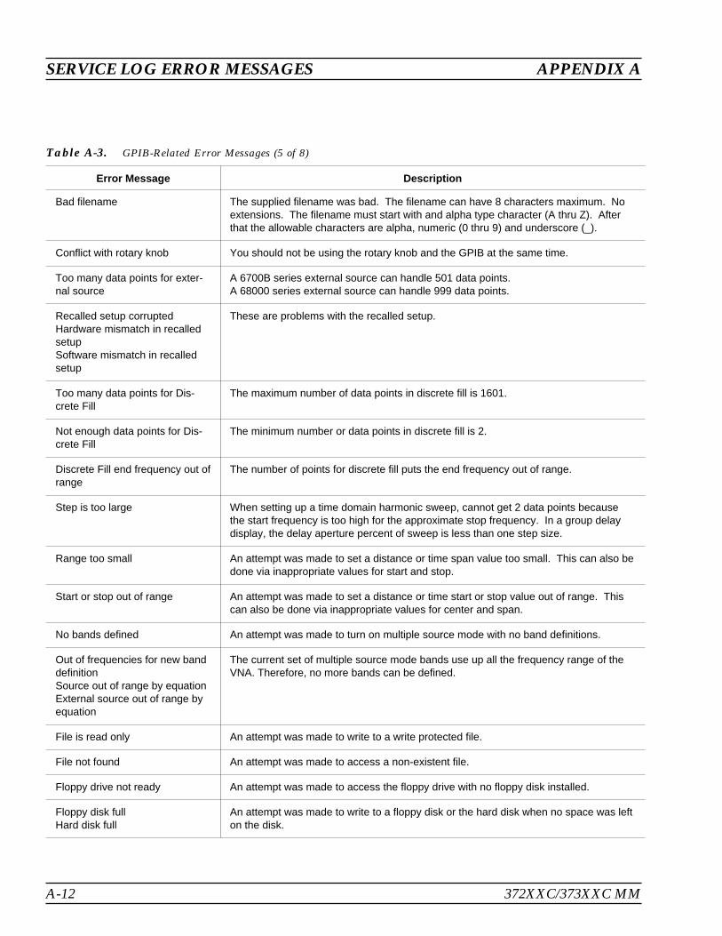
SERVICE LOG ERROR MESSAGES APPENDIX A
A-12 372XXC/373XXC MM
Error Message Description
Bad filename The supplied filename was bad. The filename can have 8 characters maximum. Noextensions. The filename must start with and alpha type character (A thru Z). Afterthat the allowable characters are alpha, numeric (0 thru 9) and underscore (_).
Conflict with rotary knob You should not be using the rotary knob and the GPIB at the same time.
Too many data points for exter-nal source
A 6700B series external source can handle 501 data points.A 68000 series external source can handle 999 data points.
Recalled setup corruptedHardware mismatch in recalledsetupSoftware mismatch in recalledsetup
These are problems with the recalled setup.
Too many data points for Dis-crete Fill
The maximum number of data points in discrete fill is 1601.
Not enough data points for Dis-crete Fill
The minimum number or data points in discrete fill is 2.
Discrete Fill end frequency out ofrange
The number of points for discrete fill puts the end frequency out of range.
Step is too large When setting up a time domain harmonic sweep, cannot get 2 data points becausethe start frequency is too high for the approximate stop frequency. In a group delaydisplay, the delay aperture percent of sweep is less than one step size.
Range too small An attempt was made to set a distance or time span value too small. This can also bedone via inappropriate values for start and stop.
Start or stop out of range An attempt was made to set a distance or time start or stop value out of range. Thiscan also be done via inappropriate values for center and span.
No bands defined An attempt was made to turn on multiple source mode with no band definitions.
Out of frequencies for new banddefinitionSource out of range by equationExternal source out of range byequation
The current set of multiple source mode bands use up all the frequency range of theVNA. Therefore, no more bands can be defined.
File is read only An attempt was made to write to a write protected file.
File not found An attempt was made to access a non-existent file.
Floppy drive not ready An attempt was made to access the floppy drive with no floppy disk installed.
Floppy disk fullHard disk full
An attempt was made to write to a floppy disk or the hard disk when no space was lefton the disk.
Table A-3. GPIB-Related Error Messages (5 of 8)

APPENDIX A SERVICE LOG ERROR MESSAGES
372XXC/373XXC MM A-13
Error Message Description
Floppy disk write protected An attempt was made to write to a write protected floppy disk.
Recalled setup or data file cor-rupt
An attempt to recall a setup from internal memory, the GPIB or disk failed due to soft-ware revision or hardware mismatch or checksum error.
New frequency list not allowed incurrent state
Cannot set up a new discrete fill definition while performing a calibration or when cor-rection is turned on. Also, cannot do this when group delay is the graph type on theactive channel.
State change not permitted An attempt was made to perform an illegal state change or action based on the cur-rent instrument state. This includes attempting to store (1) an undefined band defini-tion, (2) certain changes from the calibration state, or (3) the cal define state whendefining discrete frequencies.
Faulty label or file name The label or file name associated with the current mnemonic is faulty.
Illegal characters in filename The first character in a filename must be an alpha type. The remaining characters canbe alpha, numeric, or underscores. An extension is not permitted.
Filename too long The maximum ledngth for filenames is 8 characters. An extension is not permitted.
Floppy disk read errorFloppy disk write errorHard disk read errorHard disk write error
Read or write error(s) occurred while attempting to access the indicated disk.
Floppy disk not foundHard disk not foundGeneral disk buffer errorGeneral floppy drive failureFloppy disk init failureGeneral hard disk failureHard disk control failureHard disk init failureUnknown disk error
Other error messages which suggest that the indicated drive is in need of service.
7205 GPIB QUERY ERROR DESCRIPTIONS
No Response data available Generated if the controller attempts to read response data from the VNA and none isavailable.
No Response data after PMcompletion
This is the same as the ‘no response data available’ case above except that a pro-gram message was currently being parsed and executed when the controller at-tempted to read data. Detection of this error was deferred until the parser/executionblock was finished with the current program message and it was observed that no re-sponse data was generated.
Table A-3. GPIB-Related Error Messages (6 of 8)

SERVICE LOG ERROR MESSAGES APPENDIX A
A-14 372XXC/373XXC MM
Error Message Description
Response after Indefinite Re-sponse discarded
This error is generated when the VNA’s output queue has already received an Arbi-trary ASCII response data element and an attempt is made to place another responsedata element of any kind into the queue. The new response data element is dis-carded.
Interrupted - Response data dis-carded
This error is detected when the output queue contains unread response data and thecontroller sends a new program message. The response data is discarded.
Unterminated - Partial PM will beexecuted
This error is detected when the VNA’s input queue is currently receiving a programmessage but has not yet received the end message, and the controller attempts toread response data from the VNA. The partial program message in the input queue isexecuted as if it were properly terminated.
Deadlock - Response data dis-carded
This error is detected when both of the VNA’s input and output queues are full and thecontroller attempts to send another data byte. In order to prevent bus deadlock, thecontents of the output queue are discarded.
7205 GPIB DEVICE DEPENDENT ERROR DESCRIPTIONS
Q_SEND failure in [a procedurename]
An unsuccessful attempt was made to send a message to a task.
The procedure name is the place in the software where the error was detected.
Q_RECEIVE failure in [a proce-dure name]
A failure was detected while waiting for the reception of a message from a task.
The procedure name is the place in the software where the error was detected.
Unable to allocate memory in [aprocedure name]
An attempt was made to allocate some temporary memory in order to accomplish atask directed in the program message.
The procedure name is the place in the software where the error was detected.
Unable to release memory in [aprocedure name]
An attempt was made to return some temporary memory within a task and the returnfailed for some reason.
The procedure name is the place in the software where the error was detected.
Unable to get service/error log An unsuccessful attempt was made to get a copy of the service or error log.
Unable to get calibration term An unsuccessful attempt was made to get a calibration term.
Unable to get raw or correcteddata
An unsuccessful attempt was made to get raw or corrected data.
Unable to get final data An unsuccessful attempt was made to get final data.
Unable to get setup or data An unsuccessful attempt was made to get the frequency list from the database.
Unable to get setup An unsuccessful attempt was made to get a front panel setup.
Table A-3. GPIB-Related Error Messages (7 of 8)

APPENDIX A SERVICE LOG ERROR MESSAGES
372XXC/373XXC MM A-15
Error Message Description
Unable to store setup An unsuccessful attempt was made to save a front panel setup.
Unable to get frequency list An unsuccessful attempt was made to get setup, trace, or tabular datat from the data-base.
Unable to store label An unsuccessful attempt was made to store a label in the database.
Calibration step failure An error occurred while waiting for completion of a data collection sequence in calibra-tion.
Table A-3. GPIB-Related Error Messages (8 of 8)

SERVICE LOG ERROR MESSAGES APPENDIX A
A-16 372XXC/373XXC MM
0000 INFORMATIONAL MESSAGE
0000 SELF TEST INFO MESSAGE
0094 PRNT INTERFACE TEST PASSED
0095 PRNT INTERFACE TEST FAILED
0096 GPIB INTERFACE TEST PASSED
0097 GPIB INTERFACE TEST FAILED
0098 SELF TEST PASSED
0099 SELF TEST FAILED
0111 LO1 COMM FAIL
0112 LO1 PRE TUNE DAC FAIL
0113 LO1 PHS LCK IND FAIL
0114 PHS LCK ERR VOL OUT OF TOL
0115 LO1 LCK TIME FAIL
0211 LO2 COMM FAIL
0212 LO2 MAIN PREST DAC FAIL
0213 LO2 OFFS PREST DAC FAIL
0214 MAIN PHS LCK ERR VOL FAIL
0215 OFFST PHS LCK ERR VOL FAIL
0216 DDS PHS LCK ERR VOL FAIL
0217 MAIN PHS LCK IND FAIL
0218 OFFST PHS LCK IND FAIL
0219 DDS PHS LCK IND FAIL
0220 LO2 LCK TIME FAIL
0221 LO2 SRC TRACKING FAIL
0311 TA IF COMM FAIL
0312 TA IF 10V REF FAIL
0313 TA IF LEVEL STATUS FAIL
0314 TA PHS CONTROL FAIL
0411 REF IF COMM FAIL
0412 REF IF 10V REF FAIL
0413 REF IF LEV STATUS FAIL
0414 REF PHS CONTROL FAIL
0500 A TO D CONVERSION FAIL
0511 A TO D COMM FAIL
0512 A TO D 8 BIT D TO A FAIL
0513 A TO D 12 BIT A TO D FAIL
0514 A TO D STEERING DAC FAIL
0515 A TO D CONV ACCURACY FAIL
0516 A TO D SAMPL HOLD FAIL
0517 IF SYNC FAIL
0518 PWR SUPPLY SYNC FAIL
0519 A TO D EXT ANAL OUTP FAIL
0520 PWR SUPPLY +5V FAIL
0521 PWR SUPPLY +9V FAIL
0522 PWR SUPPLY +12V FAIL
0524 PWR SUPPLY +18V FAIL
0525 PWR SUPPLY -18V FAIL
0526 PWR SUPPLY +27V FAIL
0527 PWR SUPPLY -27V FAIL
0611 TB IF COMM FAIL
0612 TB IF 10V REF FAIL
0613 TB IF LEVEL STATUS FAIL
0614 TB PHS CONTROL FAIL
0711 LO3 COMM FAIL
0712 LO3 REF OSC FAIL
0713 LO3 48.4 LCK IND FAIL
0714 LO3 48.4 LCK ERR VOL FAIL
0715 LO3 CAL REF PHS FAIL
0811 SL SIG SEP COMM FAIL
0812 DAC ADJUSTMENT FAIL
0813 TRANSFER SWITCH CNTRL FAIL
0814 SRC LCK POL CONTROL FAIL
0815 DIRECT MODE ATTEN FAIL
0911 A9 VME BUS INTERFACE FAIL
0912 BBRAM CHECK FAIL
0913 SRAM CHECK FAIL
Table A-4. Service Log Error Messages (1 of 3)

APPENDIX A SERVICE LOG ERROR MESSAGES
372XXC/373XXC MM A-17
0914 SCSI DEVICE FAIL
0915 MCCHIP FAIL
0915 MCCHIP TIMER 1 FAIL
0916 MCCHIP TIMER 2 FAIL
0917 MCCHIP TIMER 3 FAIL
0918 MCCHIP TIMER 4 FAIL
0919 CLOCK NOT RUNNING
1311 A13 VME BUS INTERFACE FAIL
1312 EXT KEYBD CNTRL FAIL
1313 FLOPPY DISK CNTRL FAIL
1411 A14 VME BUS INTERFACE FAIL
1511 A15 VME BUS INTERFACE FAIL
1512 VRAM CHECK FAIL
1611 HARD DISK CONTROL FAIL
1811 AUXILLARY IO FAIL
1912 FRONT PANEL CNTRL FAIL
1913 ROTARY KNOB FAIL
2111 SRC COMM FAIL
2112 SRC FTUNE DAC FAIL
2113 SRC STATE MACHINE DAC FAIL
2114 SRC FM CAL FAIL
2115 SRC F TUNE PATH BND1 FAIL
2116 SRC F TUNE PATH BND2 FAIL
2117 SRC F TUNE PATH BND3 FAIL
2118 SRC F TUNE PATH BND4 FAIL
2119 SRC F TUNE PATH BND5 FAIL
2120 SRC F TUNE PATH BND6 FAIL
2121 SRC F TUNE PATH BND7 FAIL
2122 SRC F TUNE PATH BND8 FAIL
2123 SRC F TUNE PATH BND9 FAIL
2124 SRC F TUNE PATH BND10 FAIL
2125 SRC PWR LEVEL DAC FAIL
2126 SRC DETECTOR ZERO CAL FAIL
2127 SRC ALC CAL BND1 FAIL
2128 SRC ALC CAL BND2 FAIL
2129 SRC ALC CAL BND3 FAIL
2130 SRC ALC CAL BND4 FAIL
2131 SRC ALC CAL BND5 FAIL
2132 SRC ALC CAL BND6 FAIL
2133 SRC ALC CAL BND7 FAIL
2134 SRC ALC CAL BND8 FAIL
2135 SRC ALC CAL BND9 FAIL
2136 SRC ALC CAL BND10 FAIL
2137 SRC A1 FM PATH TUNE FAIL
2138 SRC A2 FM PATH TUNE FAIL
4100 LO1 CAL FAIL
4200 LO2 CAL FAIL
4301 SRC FREQ CAL MEAS UNSTABLE
4302 SRC FREQ FM MAIN CAL FAIL
4303 SRC FREQ FM SENS CAL FAIL
4304 SRC FREQ CAL VERIFY FAIL
4401 SRC ALC LOG AMP CAL FAIL
4402 SRC ALC CAL VERIFY FAIL
4500 IF CAL FAIL
4600 GAIN RANGING ERROR
4700 STATE MACHINE FAIL
5110 RF PWR UNLEVELED
5210 REF A CHAN RF OVERLOAD
5220 REF B CHAN RF OVERLOAD
5230 TA CHAN RF OVERLOAD
5240 TB CHAN RF OVERLOAD
6001 - 6128 PHASE LOCK FAILURE
7100 FILE MARKED READ ONLY
7140 GENERAL FLOPPY DRIVE FAIL
7142 FLOPPY DISK READ ERROR
7143 FLOPPY DISK WRITE ERROR
Table A-4. Service Log Error Messages (2 of 3)

SERVICE LOG ERROR MESSAGES APPENDIX A
A-18 372XXC/373XXC MM
7146 FLOPPY DISK CHANGED
7147 FLOPPY DISK UNAVAILABLE
7169 FLOPPY INIT FAIL
7170 GENERAL HARD DISK FAIL
7172 HARD DISK READ ERROR
7173 HARD DISK WRITE ERROR
7177 HARD DISK UNAVAILABLE
7199 HARD DISK INIT FAIL
7200 IEEE 488.2 GPIB BUS ERROR
7201 ABORTED MESSAGES
7202 NOTHING TO SAY
7203 NO LISTENER ON BUS
7204 GPIB COMMAND ERROR
7205 GPIB EXECUTION ERROR
7206 GPIB DEVICE SPECIFIC ERROR
7207 GPIB QUERY ERROR
7210 DEDICATED GPIB BUS ERROR
7220 PLOTTER NOT RESPONDING
7221 PLOTTER NOT READY
7222 PLOTTER OUT OF PAPER
7223 PLOTTER PEN UP
7230 POWER METER NOT RESPONDING
7240 FRQ COUNTER NOT RESPONDING
7250 EXT SOURCE NOT RESPONDING
7310 PRINTER NOT RESPONDING
7311 PRINTER NOT READY
7312 PRINTER OUT OF PAPER
7320 AUX I/O PORT ERROR
7330 SERIAL PORT ERROR
7340 ETHERNET PORT ERROR
7350 EXT TRIG RATE TOO FAST
7410 EXT KYBD ERROR
8100 PWR FAIL
8110 GENERAL VME BUS FAIL
8120 GENERAL MEMORY FAIL
8121 NON-VOLATILE MEMORY FAIL
8130 PROCESSING FAIL
8140 GENERAL DISK BUFFER ERR
Table A-4. Service Log Error Messages (3 of 3)

Table of ContentsB-1 INTRODUCTION · · · · · · · · · · · · · · · · · · · · · · · · · · · · · · · · · · · B-3
B-2 PRECAUTIONS · · · · · · · · · · · · · · · · · · · · · · · · · · · · · · · · · · · · B-3Pin Depth Problems . . . . . . . . . . . . . . . . . . . . . . . . . . . . . . . . B-3Pin-Depth Tolerance . . . . . . . . . . . . . . . . . . . . . . . . . . . . . . . B-4Avoid Over Torquing Connectors . . . . . . . . . . . . . . . . . . . . . . . . B-4Teflon Tuning Washers . . . . . . . . . . . . . . . . . . . . . . . . . . . . . . B-4Avoid Mechanical Shock . . . . . . . . . . . . . . . . . . . . . . . . . . . . . B-4Keep Connectors Clean . . . . . . . . . . . . . . . . . . . . . . . . . . . . . . B-4Visual Inspection . . . . . . . . . . . . . . . . . . . . . . . . . . . . . . . . . B-5
B-3 REPAIR/MAINTENANCE · · · · · · · · · · · · · · · · · · · · · · · · · · · · · · B-5
Appendix BConnector Care and Handling


Appendix BConnector Care and Handling
B-1 INTRODUCTION This appendix provides general, precautionary information and in-structions pertaining to precision connectors.
B-2 PRECAUTIONS The following paragraphs are precautionary notes relating to mainte-nance considerations for precision connectors
Pin Depth Problems Based on Anritsu precision components returned for repair, destruc-tive pin depth of mating connectors is the major cause of failure in thefield. When a precision component is mated with a connector having adestructive pin depth, damage will likely occur to the precision compo-nent’s connector. A connector is considered to have destructive pindepth when the center pin is too long in respect to the connector’s ref-erence plane (Figure B-1).
Before mating an unknown or new device with your VNA Port connec-tors or calibration devices, always measure the pin depth of the de-vice’s connectors. Use a Anritsu Pin Depth Gauge, or equivalent, forthese measurements (Figure B-2). Also, measure the connectorpin-depth of a device when intermittent or degraded performance issuspected.
Gauging sets for measuring the pin-depth of precision connectors areavailable from your nearest Anritsu Service center, or from the factory.Instructions for measuring connector pin-depth are included with thegauging set(s).
372XXC/373XXC MM B-3
REFERENCEPLANE
MALE
PINDEPTH
(INCHES)
REFERENCEPLANE
FEMALE
PINDEPTH
(INCHES)
Figure B-1. N Connector PinDepth Definition
01
2
3
45
1
2
3
4
21 1
2
Figure B-2. Pin Depth Gauge

Pin-Depth Tolerance The center pin of a precision connector has a tolerances measured inmils (one mil = 1/1000 inch). The connectors of test devices may not beprecision types and they may not have the proper pin-depth. Theseconnectors should be measured before mating to ensure suitability.
When gauging pin depth, if the connector being measured indicatesout of tolerance in the “+” region of the gauge (Table B-1), the centerpin is too long. Mating under this condition will likely damage the mat-ing connector. On the other hand, if the test device connector indicatesout of tolerance in the “–” region, the center pin is too short. While thiswill not cause any damage, it will result in a poor connection and aconsequent degradation in performance.
B-4 372XXC/373XXC MM
PRECAUTIONSAPPENDIX B
Port/Conn. Type
Pin Depth(MILS)
GaugeReading
GPC-7 +0.000–0.003
Same AsPin Depth
N Male 207 –0.000+0.004
207 +0.000–0.004
N Female 207 –0.004+0.000
Same AsPin Depth
3.5 mm Male, Female –0.000+0.002
K Male, Female +0.0000–0.0035
V Male +0.000to –0.001
V Female +0.000to –0.001
Table B-1. Connector Pin-Depth Tolerance

Avoid Over TorquingConnectors
Over-torquing connectors is destructive; it may damage the connectorcenter pin. Finger-tight is usually sufficient, especially on Type N con-nectors. Should it be necessary to use a wrench to tighten SMA orWSMA connectors, use a torque wrench that breaks at 8 inch-pounds.As a general rule, never use pliers to tighten connectors.
Teflon TuningWashers
The center conductor on many precision connectors contains a smallteflon tuning washer located near the point of mating (interface). Thiswasher compensates for minor impedance discontinuities at the inter-face. The washer’s location is critical to the connector’s performance.Do not disturb it.
Avoid MechanicalShock
Precision connectors are designed to withstand years of normal benchhandling. Do not drop or otherwise treat them roughly. They are labo-ratory-quality devices, and like other such devices, they require carefulhandling.
Keep ConnectorsClean
The precise geometry that makes a precision connector’s high perfor-mance possible can be disturbed by dirt and other contamination ad-hering to connector interfaces. When not in use, keep the connectorscovered.
Visual Inspection Precision connectors should be inspected periodically. Check for thefollowing:
Bent or broken center pin Damaged threads Other bent or damaged connector parts Dirt or foreign material in connector cavity.
B-3 REPAIR/MAINTENANCE Anritsu recommends that no maintenance other than cleaning be at-tempted by the customer. Any device with a suspected defective con-nector should be returned to Anritsu for repair and/or service whenneeded.
APPENDIX B REPAIR/MAINTENANCE
372XXC/373XXC MM B-5/B-6


Appendix CPerformance Specifications
This appendix contains a copy of the 37100C/37200C/37300C VectorNetwork Analyzers Technical Data Sheet, Anritsu part number11410-00247. This data sheet provides performance specifications forall of the various models in the series.


37100C/37200C/37300CVector Network AnalyzersTechnical Data Sheet
Vector Network Analysis up to 65 GHz

SYSTEM DESCRIPTIONThe Lightning 37200C/37300C Vector Network Analyzers (VNAs)are high performance tools designed to make fast and accurate S-parameter measurements of active and passive devices across the22.5 MHz to 65 GHz range. These network analyzers integrate asynthesized source, S-parameter test set and tuned receiver into asingle compact package that is ideal for bench-top testing.
The Lightning 37100C VNAs are configured as Direct-AccessReceivers for antenna, frequency conversion, and multiple outputdevice measurements. These network analyzers consist ofa synthesized source and tuned receiver in a single compact unit,with direct access provided to all four receiver samplers via the frontpanel. The 37100C offers the ultimate flexibility to meet mostreceiver measurement needs, while maintaining the ability tomeasure all four S-parameters with the addition of a reflectometersetup at the front end of the receiver.
Specifications for the 37100C/37200C/37300C models are detailedon the following pages.
High throughput measurements are achieved in each modelthrough the use of fast, 12-term error corrected sweeps, fast GPIBdata transfers and an intuitive user interface. All measurementresults are displayed on a large LCD color display or on an externalVGA monitor.
For maximum productivity, the VNAs include as standard features:
Fast Sweeping Synthesized Source Auto Reversing Test Set (37200C/37300C models only) Solid-State Transfer Switch (37200C/37300C models only) Four Independent Display Channels Multiple Source Control of Two External Sources Four Channel Receiver Internal Hard and Floppy Disk Drives LRL/LRM Calibration Adapter Removal Calibrations Fast Measurement Throughput via GPIB Built-In AutoCal® Control
Each of the network analyzers is designed for easy upgradeability.Any version of the 37000C VNA can be upgraded to accommodatenew capabilities or additional frequency ranges by ordering theappropriate upgrade kit. 37100C to 37200C or 37200C to 37300Cupgrades are also supported.
SYSTEM PERFORMANCEDynamic Range:The tables on the next page provide two definitions of dynamicrange:
"Receiver Dynamic Range" is defined as the difference between themaximum signal level at Port 2 (or at any sampler input: a1, a2, b1,or b2 for a 37100C) for 0.1 dB compression and the noise floor.
"System Dynamic Range" is defined as the difference between thepower incident on Port 2 in a through line connection and the noisefloor.
In preparing the tables, 10 Hz IF bandwidth and 512 averages wereused in calibration and measurement.
High Level Noise (typical): <0.04 dB and <0.5 degrees peak-to-peak variation in a 1 kHz IF bandwidth up to 20 GHz,<0.08 dB and <1.0 degrees peak-to-peak variation up to 40 GHz,<0.25 dB and <2.5 degrees peak-to-peak variation up to 65 GHz.
Model Numbers
2
A Reflectometer test set is available as a special option for the 37100C.It contains the transfer switch, both attenuators and couplers. It alsooffers two bias tees and a front panel amplifier loop for active devicetesting. As compared to a 37300C VNA, the output power and hence thedynamic range are degraded by 10 dB typically.
to Transfer Switch
to Test Attenuator
to Source Attenuator
InternalSourceOut*
RFIn
37100CDirect- AccessReceiver Configuration*Not provided *on Opt. 13,*Delete Source option.
SourceLockOutb1 b2a2a1
RFOut
Splitter6 dB
Samplers Source*
TransferSwitchDrive
TestAttenuatorDrive
SourceAttenuatorDrive
3 dB
Transfer Switch
DUT
TypicalReflectometerSetupSource
AttenuatorTestAttenuatorFrequency Range
37225C, 37325C 40 MHz to 13.5 GHz
37147C 22.5 MHz to 20 GHz
37247C, 37347C 40 MHz to 20 GHz
37169C 22.5 MHz to 40 GHz
37269C, 37369C 40 MHz to 40 GHz
37277C, 37377C 40 MHz to 50 GHz
37297C, 37397C 40 MHz to 65 GHz

Dynamic Range (37100C)
Dynamic Range (37200C/37300C)
37369C
37347C
37377C
7711095888575
3
Model Numbers Frequency (GHz)
37147C0.0225
220
37169C0.0225
22040-18
Model Frequency (GHz)
37147C0.0225
220
37169C
0.022522040
-18-12-12-15
-18-12-12
Maximum Signal Into ax, bx
(dBm)
-122-106-103-100
-122-106-103
Noise Floor (dBm)
104949185
1049491
Receiver Dynamic Range (dB)
1083
-3
1085
Source Power (dBm,Typical)
ModelFrequency
(GHz)
Max. Signal Into
Port 2 (dBm)
Noise Floor (dBm)
Receiver DynamicRange (dB)
37225C0.04
213.5
+20+3+3
-70-98-98
90101101
Port 1 Power (dBm,
Typical)
000
000
00
-5-15
System DynamicRange (dB)*
709898
709896
70989078
37247C0.04
220
+20+3+3
-70-98-96
9010199
37269C
0.0422040
+20+3+3+3
-70-98-95-93
901019896
0+5-2-7-2
77110958885
37277C
0.042204050
+20+3+3+3+3
-77-105-97-95-87
971081009890
0+5-2-7-2-2
37397C
+30+30+30+30+30+30
-77-105-97-95-87-77
107135127125117107
0+5-2-7-2-2
7711095888575
37297C
0.04220405065
+20+3+3+3+3+3
-77-105-97-95-87-77
97108100989080
*System Dynamic Range is based on the typical Port 1 power and specified noise floor at the indicated frequency range.
37325C0.04
213.5
+5+5+5
709896
0.04220
+30+30+30
-65-93-91
95123121
+5+5+5
+30+30+30
-65-93-93
95123123
0+50
-7
70989076
0.0422040
+30+30+30+30
-65-93-90-83
95123120113
0+5-2-7-2
77110958885
+30+30+30+30+30
-77-105-97-95-87
107135127125117
0.04220405065
0.042204050
709898

Measurement Throughput: Measurement times are based ona single 40 MHz to 20 GHz sweep with 10 kHz IF bandwidth (noaverages) after a full 12-term calibration. Sweep times includeretrace and band switch times.
Measurement Time (ms) vs. Data Points (typical)
Measurement Time vs. Sweep Mode for 101 Data Points(typical)
Measurement Time vs. IF BW for 101 Data Points (typical)
Measurement Time vs. Span for 101 Data Points (typical)
4
Test Port CharacteristicsThe specifications in the table below apply when the proper Model 34U Universal Test Port Adapters are connected, with or without phase equalinsertables, to the test set ports and calibrated with the appropriate calibration kit at 23 ± 3°C using the OSL calibration method with a sliding loadto achieve 12-term error correction (90 min. warm-up time is recommended).
Calibration Type
Data Points
1 Port (3 Term) 3000920
2 Port (12 Term)
75
300092060
3 1601
350270
340
401
250
10151
IF Bandwidth Time (ms)
10 kHz 180
1 kHz 270
100 Hz 1100
10 Hz 7300
Sweep Mode Time (ms)
Linear 350
List 350
CW 190
Frequency Span Time (ms)
40 MHz to 65 GHz 900
20 GHz to 40 GHz 340
10 GHz to 11 GHz 220
40 MHz to 40 GHz 450
Connector Frequency(GHz)
Directivity(dB)
SourceMatch(dB)
LoadMatch(dB)
ReflectionFrequency
Tracking (dB)
GPC-70.0225
218
>52>52>52
>44>44>42
>52>52>52
±0.003±0.003±0.004
GPC-7 LRL Calibration
28
>60>60
>60>60
>60>60
±0.001±0.001
N-Type*0.0225
218
>46>44>40
>36>36>32
>46>44>40
±0.004±0.004±0.005
3.5mm
0.0225220
26.5
>44>44>44>44
>40>40>38>34
>44>44>44>44
±0.005±0.005±0.006±0.006
K
0.022522040
>42>42>42>38
>40>40>38>34
>42>42>42>38
±0.005±0.005±0.006±0.006
V
0.04220405065
>40>40>40>36>34>34
>36>36>36>32>30>28
>40>40>40>36>34>34
±0.050±0.050±0.060±0.060±0.080±0.100
TransmissionFrequency
Tracking (dB)
±0.004±0.004±0.012
±0.001±0.001
±0.004±0.004±0.012
±0.030±0.030±0.050±0.070
±0.030±0.050±0.070±0.080
±0.030±0.050±0.070±0.080±0.100±0.120
Isolation(dB)
>105>115>112
>115>112
>105>115>112
>105>115>110>102
>105>115>110>100
>105>115>110>100>90>80
*Standard OSL calibration, sliding load not required.

MEASUREMENT UNCERTAINTYThe following graphs give measurement uncertainty after 12-Termvector error correction. The errors are worst case contributions ofresidual directivity, load and source match, frequency response,isolation, network analyzer dynamic accuracy, and connectorrepeatability. In preparing the following graphs, 10 Hz IF bandwidthand averaging of 512 points were used. Changes in the IFbandwidth or averaging can result in variations at low levels.
Models 37x47C Series (K-Connectors)Reflection Measurements:
Models 37x47C Series (K-Connectors)Transmission Measurements:
Device S21 (dB)
Unc
erta
inty
(dB
)
Transmission Magnitude Uncertainty37x47C/3652/Transmission Only
10
1
.1
-70 -60 -50 -40 -30 -20 -10 0 10-80-90
40 MHz2 GHz20 GHz
40 MHz2 GHz20 GHz
Transmission Phase Uncertainty37x47C/3652/Transmission Only
Unc
erta
inty
(D
egre
es)
100
10
1
.1
Device S21 (dB)-90 -80 -70 -60 -50 -40 -30 -20 -10 0 10
Reflection Magnitude Uncertainty37x47C/3652/Reflection Only
Unc
erta
inty
(dB
)
10
1
.1
-40 -35 -30 -25 -20 -15 -10 -5 0
2 GHz40 MHz20 GHz
Reflection Phase Uncertainty37x47C/3652/Reflection Only
Device S11 (dB)
Device S11 (dB)
Unc
erta
inty
(D
egre
es)
100
10
1
-40 -35 -30 -25 -20 -15 -10 -5 0
2 GHz40 MHz20 GHz
5

Models 37x69C Series (K-Connectors)Reflection Measurements:
Models 37x69C Series (K-Connectors)Transmission Measurements:
Device S21 (dB)
Unc
erta
inty
(dB
)
Transmission Magnitude Uncertainty37x69C/3652/Transmission Only
10
1
.1
-70 -60 -50 -40 -30 -20 -10 0 10-80-90
40 MHz2 GHz20 GHz40 GHz
Transmission Phase Uncertainty37x69C/3652/Transmission Only
Unc
erta
inty
(D
egre
es)
100
10
1
.1
Device S21 (dB)-90 -80 -70 -60 -50 -40 -30 -20 -10 0 10
40 MHz2 GHz20 GHz40 GHz
Reflection Magnitude Uncertainty37x69C/3652/Reflection Only
Device S11 (dB)
Unc
erta
inty
(dB
)
10
1
.1
-40 -35 -30 -25 -20 -15 -10 -5 0
40 MHz 2 GHz20 GHz40 GHz
Reflection Phase Uncertainty37x69C/3652/Reflection Only
Device S11 (dB)
Unc
erta
inty
(D
egre
es)
100
10
1
-40 -35 -30 -25 -20 -15 -10 -5 0
40 MHz 2 GHz20 GHz40 GHz
6

7
Model 37x77C and 37x97C (V-Connectors)Reflection Measurements:
Model 37x77C and 37x97C (V-Connectors)Transmission Measurements:
Device S21 (dB)
Unc
erta
inty
(dB
)
Transmission Magnitude Uncertainty37x97C/3654B/Transmission Only
10
1
.1
-70 -60 -50 -40 -30 -20 -10 0 10-80-90
40 MHz20 GHz40 GHz50 GHz65 GHz
100
10
1
Device S21 (dB)-40-50-60-70-80-90 -30 -20 -10 0 10
Transmission Phase Uncertainty37x97C/3654B/Transmission Only
40 MHz20 GHz40 GHz50 GHz65 GHz
Unc
erta
inty
(D
egre
es)
Reflection Magnitude Uncertainty37x97C/3654B/Reflection Only
Device S11 (dB)
Unc
erta
inty
(dB
)
10
1
.1
-40 -35 -30 -25 -20 -15 -10 -5 0
40 MHz20 GHz40 GHz50 GHz65 GHz
Reflection Phase Uncertainty37x97C/3654B/Reflection Only
Device S11 (dB)
Unc
erta
inty
(D
egre
es)
100
10
1
-40 -35 -30 -25 -20 -15 -10 -5 0
40 MHz20 GHz40 GHz50 GHz65 GHz

8
MEASUREMENT CAPABILITIESNumber of Channels: Four independent measurementchannels.
Parameters: S11, S21, S22, S12, or user defined combinationsof a1, a2, b1, and b2. All measurements are made without the needto manually reverse the test device. For the 37100C models, areflectometer setup at the front end of the receiver is required for S-measurements (See diagram on page 2).
Measurement Frequency Range: Frequency range of themeasurement can be narrowed within the calibration range withoutrecalibration. CW mode permits single frequency measurements,also without recalibration.
Domains: Frequency Domain, CW Draw, and optional HighSpeed Time (Distance) Domain.
Formats: Log Magnitude, Phase, Log Magnitude and Phase,Smith Chart (Impedance), Smith Chart (Admittance), Linear Polar,Log Polar, Group Delay, Linear Magnitude, Linear Magnitude andPhase, Real, Imaginary, Real and Imaginary, SWR and Power.
Data Points: 1601 maximum. Data points can be switched toa value of 801, 401, 201, 101 or 51 points without recalibration(if 1601 points were used in the calibration). In addition, the systemaccepts an arbitrary set of N discrete data points where2 ≤ N ≤ 1601. CW mode permits selection of a single datapoint without recalibration.
Reference Plane: Can be entered in time or in distance(when the dielectric constant is entered). Automatic reference planefeature adds the correct electrical length (delay) compensation atthe push of a button. Software compensation for the electricallength difference between reference and test is always accurateand stable since measurement frequencies are always synthesized.In addition, the system compensates reference phase delay fordispersive transmission media, such as waveguide and microstrip.
Markers: Six independent markers can be used to read outmeasurement data. In delta-reference mode, any one marker canbe selected as the reference for the other five. Markers can bedirected automatically to the minimum or maximum of a data trace.
Enhanced Markers: Marker search for a level or bandwidth,displaying an active marker for each channel, and discrete orcontinuous (interpolated) markers.
Marker Sweep: Sweeps upward in frequency between any twomarkers. Recalibration is not required during the marker sweep.
Limit Lines: Either single or segmented limit lines can bedisplayed. Two limit lines are available for each trace.
Single Limit Readouts: Interpolation algorithm determines theexact intersection frequencies of test data and limit lines.
Segmented Limits: A total of 20 segments (10 upper and 10lower) can be generated per data trace. Complete segmentedtraces can be offset in both frequency and amplitude.
Test Limits: Both single and segmented limits can be used forPASS/FAIL testing. The active channel's PASS or FAIL status isindicated on the display after each sweep. In addition, PASS/FAILstatus is output through the rear panel I/O connector as selectableTTL levels (PASS=0V, FAIL=+5V or PASS=+5V, FAIL=0V).
Tune Mode: Tune Mode optimizes sweep speed in tuningapplications by updating forward S-parameters more frequentlythan reverse ones. This mode allows the user to select the ratio offorward sweeps to reverse sweeps after a full 12-term calibration.The ratio of forward sweeps to reverse sweeps can be setanywhere between 1:1 and 10,000:1.
Data Averaging: 1 to 4096 averages can be selected. A front-panel button turns data averaging on/off, and an LED indicateswhen averaging is active.
Video IF Bandwidth: Front panel button selects four levels ofvideo IF bandwidth: MAXIMUM (10 kHz), NORMAL (1 kHz),REDUCED (100 Hz) and MINIMUM (10 Hz).
Trace Smoothing: Computes an average over a percentagerange of the data trace. The percentage of trace to be smoothedcan be selected from 0 to 20%. Front-panel button turns smoothingon/off, and an LED indicates when smoothing is active.
Group Delay Aperture: Defined as the frequency span overwhich the phase change is computed at a given frequency point.The aperture can be changed without recalibration. The minimumaperture is the frequency range divided by the number of points incalibration and can be increased to 20% of the frequency rangewithout recalibration. The frequency width of the aperture and thepercent of the frequency range are displayed automatically.
Group Delay Range: The maximum delay range is limited tomeasuring no more than +180° of phase change within the apertureset by the number of frequency points. A frequency step size of 100kHz corresponds to 10 ms.
DISPLAY CAPABILITIESMeasurement Channels: Four independent channels areavailable to display any S-parameter or user defined parameter, inany format, with up to two traces per channel for a maximum ofeight traces simultaneously. A single channel, two channels (1 and3, or 2 and 4), or all four channels can be displayed simultaneously.Channels 1 and 3, or channels 2 and 4 can be overlaid.
Display: Color LCD, 8.5" diagonal.
Display Colors: The color of data traces, memory, text, markersand limit lines are all user definable.
Trace Overlay: Displays two data traces on the active channel'sgraticule simultaneously.
Trace Memory: A separate memory for each channel can beused to store measurement data for later display or subtraction,addition, multiplication or division with current measurement data.
Scale Resolution (minimum per division):Log Magnitude: 0.001 dB Linear Magnitude: 1 pUPhase: 0.01° Group Delay: 0.001 psTime: 0.001 ms Distance: 0.1 µmSWR: 1 pU Power: 0.01 dBAutoscale: Automatically sets Resolution and Offset to fullydisplay measurement data.
Reference Position: Can be set at any graticule line.
Annotation: Type of measurement, vertical and horizontal scaleresolution, start/stop or center/span frequencies, and referenceposition.
Blank Frequency Information: Blanking function removes allreferences to frequencies on the display. Frequency references canonly be restored through a system reset or GPIB command.

SIGNAL SOURCE CAPABILITIESFrequency Resolution: 1 kHz (standard on all models)
Frequency Stability:Aging: <1 x 10⁻⁹/dayStability: <5 x 10⁻⁹ over 0˚ to +55˚C range
Source Power Level: The source power (dBm) may be set fromthe front panel menu or via GPIB. Check the graphs and tables onthe following pages for the range.
In addition, on 37300C models, the port 1 power may be attenuatedin 10 dB steps, using the internal 70 dB (60 dB for 37377C and37397C) step attenuator. Similarly, high input signals into port 2, notexceeding 1 watt, can be attenuated up to 40 dB, using the internalport 2 step attenuator.
Power Accuracy: ±0.5 dB at 2 GHz at default power
Power Meter Correction: The 37000C offers a user-selectablefeature that corrects for test port power variations and slope (onPort 1) using an external power meter. Power meter correction isavailable at a user-selectable power level, if it is within the poweradjustment range of the internal source. Once the test port powerhas been flattened, its level may be changed within the remainingpower adjustment range of the signal source.
Set-On Receiver Mode: The 37300C can be configured tomeasure the relative harmonic level of test devices with Set-OnReceiver Mode capability. The 37300C's unique phase lockingscheme allows it to operate as a tuned receiver by locking all of itslocal oscillators to its internal crystal reference oscillator. Set-OnReceiver Mode capability significantly increases the versatility ofthe 37300C VNA in applications that check for harmonics, intermod-ulation products, and signals of known frequency.
Multiple Source Control Capability: Multiple Source Controlcapability allows a user to independently control the frequencies oftwo sources and the receiver without the need for an externalcontroller. The frequency ranges and output powers of the twosources may be specified. A frequency sweep may be comprised ofup to five separate bands, each with independent source andreceiver settings, for convenient testing of frequency translationdevices such as mixers. Up to five sub-bands may be tested in onesweep. This feature enables users to easily test mixers, up/downconverters, multipliers, and other frequency conversion devices.
Source #1: The 37000's internal source, or any of the68XXXC, 69XXXB, 6700B or MG369XAsynthesizers
Source #2: Any of the 68XXXC, 69XXXB, 6700B orMG369XA synthesizers
Sweep Type: Linear, CW, Marker, or N-Discrete point sweep
Spurious Response (Harmonics):15 dBc (37277C, 37297C, 37325C, 37347C, 37369C,
37377C, 37397C) at maximum rated power35 dBc (all other models) at maximum rated power
Spurious Response (Nonharmonics):35 dBc at maximum rated power
Phase Noise:>60 dBc/Hz at 10 kHz offset and 20 GHz center frequency
Power Range*
Power Flatness
*Control Power for 37x25C, and 37x47C can be set to +10 dB but is notguaranteed. Similarly Control Power on the 37x69C, 37x77C, and 37x97Ccan be set to +20 dB but not guaranteed. Complete Control Power rangealso not guaranteed over temperature.
j9 Frequency Range (GHz)
9
0.0225 to 13.5 ±1.5
13.5 to 20 ±2.0
20 to 40 ±3.0
40 to 65 ±5.0
Model Rated Power (dBm)
Minimum Power (dBm)
Resolution (dB)
37147C +5 -15 0.05
37169C -3 -23 0.05
37225C 0 -20 0.05
37247C 0 -20 0.05
37269C -15 -27 0.05
37277C -7 -27 0.05
37297C -7 -19 0.05
37325C +5 -90 0.05
37347C +5 -90 0.05
37369C -7 -97 0.05
37377C -7 -87 0.05
37397C -7 -79 0.05
Flatness (dB)

10
LOG MAG 5dB/DIVRef= 0dBm
40 MHz 20 GHz
Default
AvailablePower
Model 37225C and 37247C Source Power
LOG MAG Ref= -15dBm 5dB/DIV
40 MHz 40 GHz
Model 37269C Source Power
AvailablePower
Default
LOG MAG 2dB/DIVRef= 5dBm
22.5 MHz 20 GHz
Default
AvailablePower
Model 37147C Source Power
LOG MAG Ref= -3dBm 2dB/DIV
22.5 MHz 40 GHz
Model 37169C Source Power
AvailablePower
Default
Available Source Power

11
Model 37325C and 37347C Source Power40 MHz 20 GHz
LOG MAG 5dB/DIVRef= 5dBm
AvailablePower
Default
40 MHz 40 GHz
Model 37369C Source Power
LOG MAG 5dB/DIVRef= -7dBm
AvailablePower
Default
40 MHz 65 GHz
Model 37377C and 37397C Source Power
LOG MAG 5dB/DIVRef= -7dBm
AvailablePower
Default
Available Source Power
40 MHz 65 GHz
Model 37277C and 37297C Source Power
LOG MAG 5dB/DIVRef= -7dBm
AvailablePower
Default

12
VECTOR ERROR CORRECTIONThere are five built-in methods of calibration:
1) Open-Short-Load-Thru (OSLT): This calibrationmethod uses short circuits, open circuits, and terminations(fixed or sliding).
2) Offset-Short (waveguide): This calibration method usesshort circuits and terminations.
3) LRL/LRM: The Line-Reflect-Line (LRL) or Line-Reflect-Match (LRM) calibration uses transmission lines and areflective device or termination (LRM).
4) TRM: The Thru-Reflect-Match calibration uses short circuitsand fixed termination.
5) AutoCal®: This calibration method uses an automaticcalibrator module.
There are four vector error correction models available for calibration:
1) Full 12-Term2) One Path/Two Port3) Frequency Response4) Reflection Only
Full 12-Term can be used for all models that automatically reversethe test signal. The front-panel display indicates the type ofcalibration stored in memory. A front-panel button selects whethercalibration is to be applied, and an LED lights when error correctiondata is being applied.
Calibration Sequence: Prompts the user to connect theappropriate calibration standard to Port 1 and/or Port 2. Calibrationstandards may be measured simultaneously or one at a time.
Calibration Standards: For coaxial calibrations the userselects SMA, 3.5 mm, GPC-7, Type N, 2.4 mm, TNC, K,V connector or special type from the calibration menu. Use of fixedor sliding loads can be selected for each connector type. Userdefined calibration standards allow for entry of open capacitance,load and short inductances, load impedance, and reflectionstandard offset lengths.
Reference Impedance: It is possible to modify the referenceimpedance of the measurement to other than 50Ω (but not 0).
AutoCal®: The VNA can internally control an external AutoCalmodule to perform a 2-port OSLT calibration. AutoCal is a singletwo port calibration module with built-in, switched, and charac-terized OSLT standards. AutoCal provides quick, reliable, andaccurate calibrations that exceed the performance of a standardbroadband load OSLT calibration.
LRL/LRM Calibration: The LRL calibration technique uses thecharacteristic impedance of a length of transmission line as thecalibration standard. A full LRL calibration consists merely of twotransmission line measurements, a high reflection measurement,and an isolation measurement. The LRM calibration technique is avariation of the LRL technique that utilizes a precision terminationrather than a second length of transmission line. A third optionalstandard, either Line or Match, may be measured in order to extendthe frequency range of the calibration. This extended calibrationrange is achieved by mathematically concatenating either two LRL,two LRM, or one LRL and one LRM calibration(s). Using thesetechniques, full 12-Term error correction can be performed on the37000C models.
Adapter Removal Calibration: Built-in Adapter Removalapplication software accurately characterizes and "removes" anyadapter used during calibration that will not be used for subsequentdevice measurements. This technique allows for accuratemeasurement of non-insertable devices.
Dispersion Compensation: Selectable as Coaxial (non-dispersive), Waveguide, or Microstrip (dispersive).
GAIN COMPRESSION MEASUREMENTCAPABILITY (37300C models only)The 37300C simplifies amplifier Gain Compression and AM/PMmeasurements. Once an appropriate power and frequencyschedule is selected, a power meter calibration, at a set level, willcalibrate the linear VNA receiver channels, to accurately measurepower in dBm. The 37300C supports the Anritsu, Giga-tronics, andAgilent power meters. To measure power, b2/1, a user definedparameter, is automatically selected.
Swept Power Gain Compression: The 37300C will displaytraditional Power out vs. Power in or Phase vs. Power in, at one ofup to 10 selectable frequencies. A separate screen will easily showPower out and Power in at 1 dB, or selected level GainCompression, for all entered frequencies (See figure below).
Swept Frequency Gain Compression: Once Gain ismeasured at the starting power, the user increments Power in,observing Normalized Gain vs. Frequency. This aids in analyzingthe most critical compression frequencies of a broadband amplifier.
Power Out and Phase performance as a function of Input Power ata CW frequency.
HIGH SPEED TIME (DISTANCE) DOMAINMEASUREMENT CAPABILITY (OPTION 2)Option 2A, High Speed Time (Distance) Domain software allowsthe conversion of reflection or transmission measurements fromthe frequency domain to the time domain. Measured S-parameterdata is converted to the time domain by application of a FastFourier Transform (FFT) using the Chirp Z-Transform technique.Prior to conversion, any one of several selectable windowingfunctions may be applied. Once the data is converted to the timedomain, a gating function may be applied to select the data ofinterest. The processed data may then be displayed in the timedomain with display start and stop times selected by the user orin the distance domain with display start and stop distance selectedby the user. The data may also be converted back to the frequencydomain with a time gate to view the frequency response of thegated data.
-12.00 dBm 8.00 dBm5.00000000 GHz CW
CH1 : b2/1
POWER OUT
REF = 15.000 dBm
1.000 dB/DIV CW MODE
CH3 : S21 FWD TRANS
PHASE
REF = 5.00
2.00/DIV
Phase
Power Out

13
Lowpass Mode: This mode displays a response equivalent tothe classic "TDR" (Time Domain Reflectometer) response of thedevice under test. Lowpass response may be displayed in eitherthe impulse or step mode. This type of processing requires a sweepover a harmonic series of frequencies and an extrapolated or user-entered DC value.
Bandpass Mode: This mode displays a response equivalent tothe time response of the device under test to a band limitedimpulse. This type of processing may be used with any arbitraryfrequency sweep range, limited only by the test set range or deviceunder test response.
Phasor Impulse Mode: This mode displays a response similarto the Lowpass impulse response, using data taken over anarbitrary (band limited) sweep range. Detailed information, similarto that contained in the lowpass impulse response may be used toidentify the nature of impedance discontinuities in the device undertest. Now, with Phasor Impulse, it is possible to characterizecomplex impedances on band-limited devices.
Windowing: Any one of four window functions may be applied tothe initial frequency data, to counteract the effects of processingdata with a finite bandwidth. These windows provide a range oftrade offs of main lobe width versus sidelobe level (ringing). Thegeneral type of function used is the Blackman-Harris window withthe number of terms being varied from one to four. Typicalperformance follows:
Gating: A selective gating function may be applied to the timedomain data to remove unwanted responses, either in a pass-bandor reject-band (mask). This gating function may be chosen as theconvolution of any of the above window types with a rectangulargate of user defined position and width. The gate may be specifiedby entering start and stop times or center and span. The gated datamay be displayed in the time domain, or converted back to thefrequency domain.
Time Domain Display: Data processed to time domain maybe displayed as a function of time or as a function of distance,provided the dielectric constant of the transmission media isentered correctly. In the case of dispersive media such aswaveguide or microstrip, the true distance to a discontinuity isdisplayed in the distance mode. The time display may be set to anyarbitrary range by specifying either the start and stop times or thecenter time and span. The unaliased (non-repeating) time range isgiven by the formula:
Number of Frequency Data PointsUnaliased Range (ns) = Frequency Sweep Range (GHz)
The resolution is given by the formula:
Main Lobe Width (null−null) in ns = kWFreq. Sweep Range (GHz)
where kW is two times the number of window terms (for example, four for a two-term window)
For a 40 GHz sweep range with 1601 data points, the unaliasedrange is 40.025 nanoseconds. For a 65 GHz sweep with 1601 datapoints, the unaliased range is 24.646 nanoseconds.
Frequency with Time Gate: Data that has been converted totime domain and selected by the application of gating function maybe converted back to the frequency domain. This allows the displayof the frequency response of a single element contained in thedevice under test. Frequency response accuracy is a function ofwindow and gate type, and gate width. For a full reflection,minimum gate and window accuracy is within 0.2 dB of theungated response over a 40 GHz range.
ELECTRO-OPTICALMEASUREMENT CAPABILITY(standard on all 37200/37300 models)
The 37200C/37300C series incorporated a de-embedding functionthat simplifies VNA calibration when measuring E/O and O/Edevices. Characterize the transfer function, group delay, and returnloss of optical modulators (E/O) and photo-receivers (O/E) usingthe built-in application.
E/O Measurements: The application menus guide the userthrough the entire calibration and setup. A characterized photo-diode (O/E) reference and a laser source are required to completethe test setup. The internal VNA application de-embeds theresponse of the photo-diode reference to allow direct measurementof the bandwidth and return loss of the modulator.
O/E Measurements: Photo-receiver measurements can bemade by characterizing a modulator first and then using it as atransfer standard for the O/E measurement. The internal applicationde-embeds the response of the modulator to allow characterizationof the photo-receiver.
Type of Window(Number of Terms)
First Side Lobe Relative to Peak
Rectangle (1) -13 dB
Nominal-Hamming (2) -43 dB
Low Side Lobe,Blackman-Harris (3) -67 dB
Minimum Side Lobe,Blackman-Harris (4) -92 dB 2.7W
2.1W
1.8W
1.2W
Impulse Width1
1W(Bin Width) = 1/2∆f sweep width.Example. When ∆f = 40 MHz to 40 GHz, W = 12.5 ps
When ∆f = 40 MHz to 65 GHz, W = 7.7 ps

14
GPIBGPIB INTERFACES: 2 Ports, system GPIB and dedicatedGPIB
System GPIB (IEEE-488.2): Connects to an externalcontroller for use in remote programming of the networkanalyzer. Address can be set from the front panel and canrange from 1 to 30.Dedicated GPIB: Connects to external peripherals fornetwork analyzer controlled operations (e.g., GPIB plotters,frequency counters, frequency synthesizers and power meters).
Interface Function Codes: SH1, AH1, T6, TE0, L4, LE0, SR1,RL1, PP1, DT1, DC0, and C0.
GPIB Data Transfer Formats: ASCII, 32-bit floating point, or64-bit floating point. 32-bit and 64-bit floating point data can betransferred with LSB or MSB first.
GPIB Data Transfer Speed (with or without cal):150 kbyte/sec
GPIB Data Throughput Time: Throughput measurements forboth tables were made as follows: start the timer, trigger a sweep,wait for a full sweep, transfer data across the GPIB and stop thetimer. Data throughput times are shown separately formeasurements made without calibration and with full two-port,12-Term calibration. Measurement conditions: 40 MHz to 20 GHzsweep, single channel, log magnitude display, 10 kHz IF bandwidth,and output final data.
Throughput Times (ms) without Correction (typical)
Throughput Times (ms) with 12-Term Correction (typical)
Fast CW Operation: Fast CW is an ideal mode of operation forrapid data taking over GPIB. To achieve a fast measurement ratethe display is not updated and only the raw S-parameter or user-defined parameter of the active channel is measured.
Fast CW Typical Performance
Internal Buffer Data Collection: Internal Buffer DataCollection is provided to allow saving active channel measurementdata from multiple sweeps without having to synchronize andcollect data at the end of each sweep. The 37000C can store up to50,000 data point measurements, each consisting of two (real andimaginary) IEEE 754 4-byte floating point numbers. GPIB transferspeed for the 50,000 data points is typically 2.2 seconds.
STORAGE
Internal Memory: Ten front panel states (no calibration) can bestored and recalled from non-volatile memory locations. The currentfront panel setup is automatically stored in non-volatile memory atinstrument power-down. When power is applied, the instrumentreturns to its last front panel setup.
Internal Hard Disk Drive: 340 MB mininum, used to store andrecall measurement and calibration data and front-panel setups. Allfiles are MS-DOS® compatible. File names can be 1 to 8 characterslong, and must begin with a character, not a number. Extensionsare automatically assigned.
External SCSI Interface: Option 4 deletes the internal harddisk drive, and adds a SCSI Interface connector to the rear panelfor connecting a SCSI-2 formatted hard disk drive.
Internal Floppy Disk Drive: A 3.5-inch diskette drive with1.44 Mbytes formatted capacity is used to load measurementprograms and to store and recall measurement and calibrationdata and front-panel setups. Measurement data can be stored intext, S2P or bitmap format. All files are MS-DOS compatible.File names can be 1 to 8 characters long and must begin with acharacter, not a number. Extensions are automatically assigned.
Measurement Data: 102.8 kbytes per 1601 point S-parameterdata file.
Calibration Data: 187.3 kbytes per 1601 point S-parameterdata file (12-Term cal plus setup).
Trace Memory File: 12.8 kbytes per 1601 point channel.
HARD COPYPrinter: A menu selects full screen, graphical, tabular data, andprinter type. The number of data points of tabular data can beselected as well as data at markers only. Compatible with mostHP and Epson printers with parallel (Centronics) interfaces.
GPIB Plotter: The 37000 is compatible with most HP andTektronix plotters. A menu selects plotting of full or user-selectedportions of graphical data. The plotter is connected to the dedicatedGPIB bus.
Performance: After selecting the Start Print button, front paneloperation and measurement capability is restored to the user withintwo seconds.
Data Format 3 Points* 101 Points 401 Points 1601 Points
32 Bit 150 500 1200 3600
64 Bit 150 500 1200 3600
ASCII 150 600 1500 4400
3 Points* 101 Points 401 Points 1601 Points
190 950 2300 6900
190 950 2300 6900
190 1000 2500 7400
*3 data point sweeps taken at 2, 4, and 6 GHz
Trigger Mode Measurement Speed (ms/point)
GPIB 1.5
External TTL 1.2
Internal 0.8
Data Format
32 Bit
64 Bit
ASCII
*3 data point sweeps taken at 2, 4, and 6 GHz

15
INTERFACES37000C Front Panel Connectors and Controls:
Keyboard Input: An IBM-AT compatible keyboard can beconnected to the front panel for navigating through front panelmenus, annotation of data files and display labels, printingdisplays and pausing instrument sweeps.Test Ports (37200C and 37300C): Universal K male testports are standard on all models except for the >40 GHz modelswhich have Universal V male test ports as standard. Foradditional configurations check Test Port Converters (Option 7).Bias Inputs, Port 1 and 2 (37300C): 0.5 amps maximumthrough BNC connectors.Source Input Loop (37100C): Provides external sourceinput capability, replacing the internal source.RF Output (37100C): K, female, provides source RF output.a1, a2, b1, b2 Inputs (37100C): K, female, provide inputs tothe samplers.Source Lock Output (37100C): Provides a sample of theinternal source, at -9 dB (typical) relative to the internal sourcepower.Port 1 Amplifier Loop (37300C): Provides access toinsert an external amplifier, ahead of the port 1 coupler orbridge, to increase port 1 power output, up to +30 dBm(1 watt) maximum.
37000C Rear Panel Connectors and Controls:PRINTER OUT: Centronics interface for an external printer.VGA OUT: Provides VGA output of 37000C video display.SERIAL: 9-Pin male DSUB connector. Provides RS-232 serialport control for an AutoCal® module (3658 series).10 MHz REF IN: Connects to external reference frequencystandard, 10 MHz, +5 to -5 dBm, 50Ω, BNC female.10 MHz REF OUT: Connects to internal reference frequencystandard, 10 MHz, 0 dBm, 50Ω, BNC female.EXT ANALOG OUT: -10V to +10V with 5 mV resolution,varying in proportion to user-selected data (e.g., frequency,amplitude). BNC female.EXT ANALOG IN: ±50 volt input for displaying externalsignals on the LCD. BNC female.LINE SELECTION: Power supply automatically senses100V, 120V, 220V or 240V lines.EXTERNAL TRIGGER: External TTL triggering for 37000Cmeasurement. 10 kΩ input impedance, BNC female.
REFERENCE EXTENSION: The 37300C provides accessto the a1 and b1 samplers as standard. The 37200C providesaccess to a1 as an option. K female connectors are used,except for >40 GHz models where V female connectorsare used.EXTERNAL SCSI: Provides SCSI-2 connector forconnection of an external SCSI hard disk drive (Option 4).EXTERNAL I/O: 25-pin DSUB connector.LIMITS PASS/FAIL: Selectable TTL levels (Pass=0V,Fail=+5V or Pass=+5V, Fail=0V. Additionally, 0 volts(all displayed channels pass) or +5V (any one of four displayedchannels fail) output pass/fail status (1 line).PORT 1 SOURCE ATTENUATOR (37100C): Drive signalfor a source external programmable step attenuator.PORT 2 TEST ATTENUATOR (37100C): Drive signal fora test external programmable step attenuator.TRANSFER SWITCH (37100C): Drive signal for anexternal transfer switch.
GENERAL
Power Requirements: 85-240 volts, 48-63 Hz,540 VA maximum
Dimensions: 267 H x 432 W x 585 D mm (10.5 H x 17 W x 23 D in.)
Weight: 27 kg (60 lb)-(2-man lift required)
Storage Temperature Range: -40°C to +75°C
Operating Temperature Range: 0°C to +50°C
Relative Humidity: 5% to 95% at +40°C
EMI: Meets the emissions and immunity requirements ofEN55011/1991 Class A/CISPR-11 Class A
EN50082-1/1993
IEC 801-2/1984 (4 kV CD, 8 kV AD)IEC 1000-4-3/1995 (3 V/m, 80-1000 MHz)IEC 801-4/1988 (500V SL, 1000V PL)IEC 1000-4-5/1995 (2 kV L-E, 1 kV L-L)

©Anritsu January 2003; Rev: C 11410-00247Data subject to change without notice 37100C/37200C/37300C Vector Network Analyzers Technical Data Sheet
Microwave Measurements Division • 490 Jarvis Drive • Morgan Hill, CA 95037-2809http://www.us.anritsu.com • FAX (408) 778-0239
Sales Centers:United States (800) ANRITSUCanada (800) ANRITSUSouth America 55 (21) 286-9141
Sales Centers:Europe 44 (0) 1582 433433Japan 81 (03) 3446-1111Asia-Pacific 65-2822400
LRL/LRM-Calibration method of Rohde & Schwarz, GermanyGPC−7 is a registered trademark of Amphenol Corporation.K Connector and V Connector are registered trademarks of Anritsu Company.AutoCal is a registered trademark of Anritsu Company.

Table of Contents
D-1 INTRODUCTION · · · · · · · · · · · · · · · · · · · · · · · · · · · · · · · · · · · D-3
D-2 ME7808A OPERATING SOFTWARE · · · · · · · · · · · · · · · · · · · · · · · · D-3
D-3 SYSTEM DESCRIPTION · · · · · · · · · · · · · · · · · · · · · · · · · · · · · · · D-4
D-4 SYSTEM ADJUSTMENTS · · · · · · · · · · · · · · · · · · · · · · · · · · · · · · D-4
D-5 REPLACEABLE ITEMS · · · · · · · · · · · · · · · · · · · · · · · · · · · · · · · D-6
D-6 PERFORMANCE VERIFICATION/SYSTEM OPERATIONAL TESTS · · · · · · D-8
D-7 MULTIPLEXING COUPLER CHECK · · · · · · · · · · · · · · · · · · · · · · · D-22
D-8 TROUBLESHOOTING · · · · · · · · · · · · · · · · · · · · · · · · · · · · · · · D-24
Appendix DME7808A BroadbandMeasurement SystemMaintenance


Appendix DME7808A BroadbandMeasurement SystemMaintenance
D-1 INTRODUCTION This appendix provides maintenance instructions for the ME7808ABroadband Measurement System. It describes Maintenance and Per-formance Verification of the ME7808A Broadband VNA system. Thismaintenance and verification is performed independently of any wa-fer-probe station. Models 37397C and 37297C are completely inter-changeable in this system, and several models of synthesizers may beused with this system. All have identical operating characteristicswithin the ME7808A system, regardless of the labels in this appendix.
On early systems, many instruments were labeled with SM numbers,rather than typical Anritsu model designations. The operating charac-teristics of the SM units are identical in most cases to the operation ofthe newer models. The following SM numbers are supported by thisappendix:
SM5621 (modifications to the 37397C)
SM5645 (3742A-EW Millimeter Module)
SM5620 (3738A Test Set)
SC6195 (57215, 57216 Couplers)
D-2 ME7808A OPERATINGSOFTWARE
On early ME7808A systems, software installed into the 37397C waslabeled as various versions of 3.6x. This was intended to be temporarysoftware only and the 37397C BMS should be upgraded to at least ver-sion 4.00 to achieve best system performance.
APPENDIX D INTRODUCTION
372XXC/373XXC MM D-3

D-3 SYSTEM DESCRIPTION Figure D-3 (next page) shows the functional block diagram of the en-tire ME7808A system (excluding probe station). See Section D-8 Trou-bleshooting for more detailed information.
D-4 SYSTEMADJUSTMENTS
Anritsu recommends that the system be readjusted and the perfor-mance be verified every 12 months. The 37397C instrument and theSynthesizers require adjustment (recalibration). The 3742A modulesand the 3738A Test Set are not adjustable.
The 37397C instrument adjustments are performed with the systemoperating in the Internal mode (40 MHz to 65 GHz only). Refer toChapter 6 of this manual for complete instructions on readjustment ofthe 37397C instrument.
Refer to the 68000C Maintenance Manual (part number 10370-10336)for adjustment and verification of those synthesizers.
Refer to the MG3690A Maintenance Manual (part number10370-10355) for adjustment and verification of those synthesizers.
SYSTEM DESCRIPTION APPENDIX D
D-4 372XXC/373XXC MM

372XXC/373XXC MM D-5
APPENDIX F SYSTEM ADJUSTMENTS
L
57215 Coupler(SC6195)
57216 Coupler(SC6195)
DUT
with Opt. 15AAddress 4 (Upper)
Local Oscillator8.12 to 13.75GHz
+17 dBm
Address 5 (lower)RF
10.83 to 18.33GHz+13 dBm
RF Source(YIG oscillator, doubler,
quadruplers)
40MHz to 65GHz
Receiver(Local Oscillators, Mixers)
GaAsSwitch
GaAsSwitch
GaAsSwitch
GaAsSwitch
Splitter
Transfer Switch(Selects Port 1 or
Port 2)
PowerSupply
(+15 VDC)
Control PCB(+12, -5
VDC)
X8
X6 X6
X8Mixer Mixer
Port 1 3742A-EW mm Module(SM5645)
Port 2 3742A-EW mmModule(SM5645)
3738A
37000C VNAwith Option 12
(SM5621)
"Test" fromPort 1 Module
(270MHz)
Ref A fromPort 1 Module
(270MHz)
MG3692A or68037C Synth
MG3692A or68037C Synth
Ref A(270MHz) LO RF LORF
Ref B(270MHz)
MixerMixer
Port 1 Port 2
Port 2 "Test"(270 MHz)
Port 1 "Test"(270 MHz)
40MHz to65GHz
40MHz to65GHz
40MHz to65GHz
40MHz to110GHz
40MHz to110GHz
IFAmp
IFAmp
IFAmp
IFAmp
BroadbandTest Set(SM5620)
L
R
IF IF IF IF
R
L65 - 110
GHz
b2
a2
a1
b1
LO RF a1 a2b1 b2
65 - 110GHz
L
R L R
3738ARearPanel
to 3738A front panel
Isolator
Figure D-3. ME7808A Block Diagram

D-5 REPLACEABLE ITEMS Part numbers and descriptions of ME7808A replaceable system cablesand parts and shown in Tables D-2 and D-3. Replacement parts andsubassemblies for the 37000C VNA are shown in Chapter 2 of thismanual. Replacement parts and subassemblies for the MG3690 or68000 Synthesizers are shown in the applicable synthesizer mainte-nance manual.
NOTEThere are no serviceable components or subassemblies inthe 3742A modules or in the 57215/57216 couplers. Theseitems must be returned to Anritsu Customer Service for re-pair or replacement.
REPLACEABLE ITEMS APPENDIX D
D-6 372XXC/373XXC MM
Description Part Number
RF Cable, Ruggedized, Synthesizer to 3738A LO IN ND46621 (68000 series synthesizers only)
RF Cable, Ruggedized, Synthesizer to 3738A RF IN ND46620 (68000 series synthesizers only)
RF Cable, Coupler to 37000 806-101
Cable Set, rear panel, 37000 ND58267
Cable Set, 3742A to 3738A ND58268
Cable, GPIB 2100-2
RF Cable, Ruggedized, Synthesizer to 3738A LO IN C34429-7 (MG series synthesizers only)
RF Cable, Ruggedized, Synthesizer to 3738A RF IN C34429-8 (MG series synthesizers only)
Multiplexing Coupler, Left (Port 1) 57215
Multiplexing Coupler, Right (Port 2) 57216
Table D-2. System Cables

APPENDIX D REPLACEABLE ITEMS
372XXC/373XXC MM D-7
Description Part Number
Power Supply (+15VDC) 40-130
Fan Assembly ND58282
IF Amplifiers 60-136
IF Switches 1020-44
Isolator 1000-49
RF Splitter 1091-87
PCB Assembly 54074-3
Transfer Switch ND57971
Table D-3. Model 3738A Replaceable Parts

D-6 PERFORMANCEVERIFICATION/SYSTEMOPERATIONAL TESTS
This chapter describes a series of manually performed tests that willensure that the system meets many factory specifications. Many ofthese tests are also duplicated in the 2300-178 software package (ver-sion 4.10 and above).
Two automated methods are also available for S-parameter measure-ment accuracy testing (Performance Verification). The test port typebeing utilized will determine which method is appropriate.
NOTEAnritsu does not support tests or verification processes forwafer probe equipment. Contact the vendor of the waferprobe equipment if such support is desired.
For systems utilizing the W1 coaxial test ports (57215/57216 orSC6195 couplers), performance verification of the system is accom-plished by use of the Anritsu Model 3656 calibration/verification kitand the 2300-496 software (packaged with the kit). This series of auto-mated tests will verify that the system S-parameter measurement ac-curacy meets factory specifications. Instructions are packaged withinthe software as an Adobe Acrobat file.
For systems using only WR10 waveguide test ports, NIST traceableverification of S-parameter measurement accuracy may be performedfor the system (including a WR10 calibration kit). Contact AnritsuCustomer Service in Morgan Hill, California for information about thisservice.
The balance of this section is dedicated to operational performancetests of the complete ME7808A system.
PERFORMANCE/OPERATIONAL TESTS APPENDIX D
D-8 372XXC/373XXC MM

Required Equipment for ME7808A System Performance Tests
PC with Windows 95 or equivalent operating system
National Instruments GPIB hardware and software installed inthe PC
Anritsu 2300-178 (3700TEST) Software
Anritsu 3654B Calibration Kit
Anritsu 3670V50-2 RF Cable (Throughline)
Anritsu 3655W (WR10) Calibration Kit orMaury Z7005G19 (WR10) Calibration Kit
Optional Equipment
HP Model 432A Power Meter with power sensor(s) covering 65 to110 GHz
Anritsu model SC6291 Male-Male adapter (for verifying the Cou-plers)
Voltmeter (for troubleshooting only)
Anritsu ML24xx Power Meter with 20 GHz Power Sensor (fortroubleshooting only)
Preliminary
Step 1. Move millimeter modules and cables to another location sothat the PC keyboard and the 37000C front panel are eas-ily accessible.
Step 2. Press the Option Menu key.
Step 3. Select TEST SET CONFIG / INTERNAL, then press<Enter> to accept.
Step 4. On the rear panel of the 37000C, remove the cable setwhich connects to the 3738A, and install the small termina-tions (hanging from the chains) to the SMA connectors onthe back of the 37000C.
Step 5. Load and run the 2300-178 test software, then the2300-496 Veriication software. More complete instructions,such as required GPIB settings, are found in the Users’Guide contained within the 2300-496 software.
Synthesizer Verification
Refer to the appropriate Maintenance Manual for the synthesizers in-stalled in the system for detailed Verification instructions. No furtherchecks are necessary in the ME7808A system.
APPENDIX D PERFORMANCE/OPERATIONAL TESTS
372XXC/373XXC MM D-9

Millimeter Wave Module Verification
Most specifications for the system when operating from 65 to 110 GHzare not published (guaranteed) but are typical values. Systems whichpass the following tests are operating in the expected manner and arecapable of making accurate measurements.
Assemble the complete system with the 3742A modules installed, withall front and rear panel cables reconnected. Then perform the follow-ing steps.
Step 1. Configure system as a 65-110 GHz system. To do this, pressthe Utility Menu and select TEST SET CONFIG / MILLI-METER WAVE and press the <Enter> key. Select theWR-10 Extended band.
Step 2. Set the power vernier knobs on the 3742A modules fullyCW to set maximum power at the test ports.
Step 3. Remove the 57215 and 57216 Couplers from the mmWavemodules. Insure the 2 inch gold waveguide sections are in-stalled to the test ports of the mmWave modules.
Step 4. Connect the two modules together.
Step 5. View S21 and S12.
Step 6. Ensure the system sweeps normally in this mode.
Step 7. Ensure both power control knobs on the mmWave modulesare functional. It is normal for Lock Failures to appear atlower power. Return power control knobs to maximumpower settings.
Step 8. Clear the errors from the Service Log.
PERFORMANCE/OPERATIONAL TESTS APPENDIX D
D-10 372XXC/373XXC MM

IF Power Level Test
This test verifies that each individual receiver channel operates prop-erly. Measurement calibration of the system is not required for thistest. Ensure the system has warmed up for at least 1 hour before per-forming this test.
Step 1. Install a flush short on the test port of the Port 1 mmWavemodule.
Step 2. Set up the network analyzer as shown below:
Key Menu Choice
SETUP MENU Start: 65 GHz
Stop: 110 GHz
CHANNEL MENU Dual Channels 1 & 3
GRAPH TYPE Log Magnitude (both channels)
S PARAMS Channel 1
User Ratio: a1/1
User Phase Lock: a1
Channel 3
User Ratio: b1/1
User Phase Lock: a1
SET SCALE Resolution: 10 dB/Div (both channels)
Reference Value: -10 dB
LIMITS Channel 1 (a1/1)
Upper Limit: ON (-1 dB)
Lower Limit: ON (-28 dB )
Channel 3 (b1/1)
Upper Limit: ON (-1 dB)
Lower Limit: ON (-38 dB)
Step 3. Ensure that the displays for Channels 1 and 3 fall betweenthe limit lines, and that no error messages appear on thedisplay.
Step 4. Install a flush short to the Port 2 mmWave module.
APPENDIX D PERFORMANCE/OPERATIONAL TESTS
372XXC/373XXC MM D-11
Step 5. Set up the network analyzer as shown below:
Key Menu Choice
SETUP MENU Start: 65 GHz
Stop: 110 GHz
CHANNEL MENU Dual Channels 2 & 4
GRAPH TYPE Log Magnitude (both channels)
S PARAMS Channel 2
User Ratio: a2/1
User Phase Lock: a2
Channel 4
User Ratio: b2/1
User Phase Lock: a2
SET SCALE Resolution: 10 dB/Div (both channels)
Reference Value: -10 dB
LIMITS Channel 2 (a2/1)
Upper Limit: ON (-1 dB)
Lower Limit: ON (-28 dB )
Channel 4 (b2/1)
Upper Limit: ON (-1 dB)
Lower Limit: ON (-38 dB)
Step 6. Ensure that the displays for Channels 2 and 4 fall betweenthe limit lines, and that no error messages appear on thedisplay.
PERFORMANCE/OPERATIONAL TESTS APPENDIX D
D-12 372XXC/373XXC MM

Test Port Power Test
Step 1. Default the system (Press Default Program key two times).Display Single Channel, S11.
Step 2. Connect the HP432A Power Meter and sensor to the Port 1mmWave module test port.
Step 3. For each frequency on the power sensor, read the power atthe Port 1. The power should be 0 to -10 dBm for each fre-quency.
Step 4. Display Single Channel, S22. Connect the power sensor toPort 2. Repeat steps 2 and 3 for the Port 2 module.
Performance Verification- High Level Noise (Reflection) Test
The following test verifies that the high level noise in the system willnot significantly affect the accuracy of subsequent measurements.High level noise is the random noise that exists in the system, andcannot be accurately predicted or measured, thus it cannot be removedby conventional error-correction techniques. Measurement calibrationis not required for these tests. Ensure the system has warmed up forat least 1 hour before performing this test.
Step 1. Connect flush shorts to both test ports of the mmWavemodules.
Step 2. Default the system (press DEFAULT PROGRAM twotimes).
Step 3. Set the system as shown below:
Key Menu Choice
SETUP MENU Start: 65 GHz
Stop: 110 GHz
CHANNEL MENU Dual Channels 1 & 3
GRAPH TYPE Log Magnitude (both channels)
S PARAMS Channel 1: S11
Channel 3: S22
SET SCALE Resolution: 0.05 dB/division (bothchannels)
LIMITS Channel 1
Upper Limit: ON (0.04 dB)
Lower Limit: ON (-0.04 dB )
Channel 3
Upper Limit: ON (0.04 dB)
Lower Limit: ON (-0.04 dB )
APPENDIX D PERFORMANCE/OPERATIONAL TESTS
372XXC/373XXC MM D-13

Step 4. Be careful not to bump any system components (especiallycables) during this test. Select Channel 1. After severalsweeps, press TRACE MEMORY, and select Store Data toMemory. Select View Data/Memory.
Step 5. Be sure the RF display remains between the limit lines forapproximately 5 sweeps. (It is normal for the data to driftout of the limit lines after a short period of time).
Step 6. Repeat steps 4 and 5 for Channel 3.
Performance Verification- High Level Noise (Transmission) Test
The following test verifies that the high level noise in the system willnot significantly affect the accuracy of subsequent measurements.High level noise is the random noise that exists in the system. It can-not be accurately predicted or measured, thus it cannot be removed byconventional error-correction techniques. Measurement calibration isnot required for these tests. Ensure the system has warmed up for atleast 1 hour before performing this test.
Step 1. Remove the flush shorts and connect the mmWave modulestogether.
Step 2. Set the system as shown below:
Key Menu Choice
SETUP MENU Start: 65 GHz
Stop: 110 GHz
CHANNEL MENU Dual Channels 1 & 3
GRAPH TYPE Log Magnitude (both channels)
S PARAMS Channel 1: S12
Channel 3: S21
SET SCALE Resolution: 0.05 dB/division (bothchannels)
LIMITS Channel 1
Upper Limit: ON (0.04 dB)
Lower Limit: ON (-0.04 dB )
Channel 3
Upper Limit: ON (0.04 dB)
Lower Limit: ON (-0.04 dB )
Step 3. Be careful not to bump any system components (especiallycables) during this test. Select Channel 1.
PERFORMANCE/OPERATIONAL TESTS APPENDIX D
D-14 372XXC/373XXC MM

Step 4. After several sweeps, press TRACE MEMORY, and selectStore Data to Memory. Select View Data/Memory.
Step 5. Be sure the RF display remains between the limit lines forapproximately 5 sweeps. (It is normal for the data to driftout of the limit lines after a short period of time).
Step 6. Repeat steps 3 and 4 for Channel 3.
Drift Test
Step 1. Leave the equipment connected as described in the previ-ous test (High Level Noise Transmission). Ensure the sys-tem has warmed up for 2 hours.
Step 2. Change Graph Type to Log Mag and Phase for both chan-nels.
Step 3. Store Data to Memory and View Data/Memory for bothchannels.
CAUTIONDo not move any part of the system afterthis point. Be especially careful to not bumpthe cables.
Step 4. At the end of 1/2 hours, Autoscale both channels.
Step 5. Set Limit Lines to +/- 0.2 dB, and +/- 2 Degrees for bothchannels. Ensure displays fall within the limit lines.
APPENDIX D PERFORMANCE/OPERATIONAL TESTS
372XXC/373XXC MM D-15

Performance Verification- 12 Term OSL Calibration
This calibration is required to perform the System Dynamic Range,Source Match, and Directivity tests. Ensure the system has warmedup for at least 1 hour before performing this test, and that the preci-sion 2 inch waveguide sections are installed to the test ports of themmWave modules.
Step 1. Insert the Calibration Coefficient disk from the WR-10 cali-bration kit into the floppy drive of the 37397C and load thecoefficients via the UTILITY MENU key.
Step 2. Press BEGIN CAL.
Step 3. Make the following selections from the menus to perform afull band 12 Term Calibration:
Change Cal Method and Line Type
Waveguide
Full 12 Term
Include Isolation (required for System Dynamic Rangetest)
Sliding Load (required for Directivity and Source Matchtests)
Use Installed Kit
Step 4. Before measuring the Isolation Devices (terminations),make the following changes to the setup:
AVERAGE/SMOOTH MENU key: Change to 512 aver-ages
IFBW key: Change to Minimum (10 Hz)
Measure the Isolation Devices.
Step 5. Finish the calibration using the instructions on the VNAdisplay.
PERFORMANCE/OPERATIONAL TESTS APPENDIX D
D-16 372XXC/373XXC MM

Performance Verification- Source Match and Directivity Tests
Ensure the 12 Term Calibration was performed as described above(sliding loads were used) and the calibration is active (APPLY CALLED is ON). During this test, do not disconnect the gold waveguidesections which were used during the 12 Term Calibration.
Source Match Test
Step 1. Set up system as shown below:
Key Menu Choice
SETUP MENU Start: 65 GHzStop: 110 GHz
CHANNEL MENU Single ChannelChannel 1
GRAPH TYPE Log Magnitude
SET SCALE Resolution:0.1 dB/DIV
Ref Value:0.0 dB
Reference Line:TOP
S-PARAMS S11
Step 2. Attach a second high-precision waveguide section to themodule on Port 1.
Step 3. Attach a flush short to the end of the high-precision wave-guide section.
Step 4. While observing the sweep indicator, allow at least onecomplete sweep to occur. Press Autoscale to center thetrace.
Step 5. Press Marker Menu, and select MARKER 1, MARKER 2,and MARKER 3, to be ON.
Step 6. Using the rotary knob, position marker 1 and marker 2 toadjacent peaks of the ripple with the greatest negativetrough (or adjacent troughs if the ripple has the greatestpositive peak); position marker 3 to the bottom of thetrough (or the top of the peak if the ripple has the greatestpositive peak). Refer to Figure D-3 (following page).
APPENDIX D PERFORMANCE/OPERATIONAL TESTS
372XXC/373XXC MM D-17

Step 7. Using the Marker Menu and Readout Marker key menus,record the absolute value of markers 1 and 2 as follows:
Subtract one from the other.
Halve the difference
Add the resultant to the value of the marker at the low-est peak (or the deepest trough).
This is the average value of the two peaks (or troughs).
Step 8. Record the marker 3 value.
Step 9. Find the absolute difference of the values recorded in step 7and step 8. This is the Peak-to-Peak Ripple value. Use theRF Measurement Chart (Table D-3) to find the correspond-ing Return Loss value. This value is the Effective SourceMatch. Insure Source Match measures at least 30 dB.
Step 10. Change the S Parameter to S22. Move the outside wave-guide section with the short attached to the Port 2 module.
Step 11. Repeat Steps 4 through 9 to compute Port 2 Source Match.Verify Port 2 Source Match is 30 dB minimum.
PERFORMANCE/OPERATIONAL TESTS APPENDIX D
D-18 372XXC/373XXC MM
Figure D-3. Markers
MARKER
MARKER
65.000000 GHz 110.000000

APPENDIX D PERFORMANCE/OPERATIONAL TESTS
372XXC/373XXC MM D-19
Relative to Unity Reference
SWR ReflectionCoefficient
ReturnLoss(dB)
XdB BelowReference
REF + XdB
REF – XdB
REF XPeak to Peak Rip-
ple dB
17.39108.72425.84804.41943.5698
0.89130.79430.70790.63100.5623
12345
12345
5.53505.07804.64954.24893.8755
–19.2715–13.7365–10.6907–8.6585–7.1773
24.806518.814515.340212.907311.0528
3.00952.61462.32292.09991.9250
0.50120.44670.39810.35480.3162
678910
678910
3.52873.20752.91082.63762.3866
–6.0412–5.1405–4.4096–3.8063–3.3018
9.56998.34807.32046.44395.6884
1.78491.67091.57691.49851.4326
0.28180.25120.22390.19950.1778
1112131415
1112131415
2.15671.94651.75471.58021.4216
–2.8756–2.5126–2.2013–1.9331–1.7007
5.03224.45903.95613.51333.1224
1.37671.32901.28801.25281.2222
0.15850.14130.12590.11220.1000
1617181920
1617181920
1.27781.14761.02990.92370.8279
–1.4988–1.3227–1.1687–1.0337–0.9151
2.77662.47032.19861.95741.7430
1.19571.17261.15241.13471.1192
0.08910.07940.07080.06310.0562
2122232425
2122232425
0.74160.66390.59410.53140.4752
–0.8108–0.7189–0.6378–0.5661–0.5027
1.55241.38281.23191.09750.9779
1.10551.09351.08291.07361.0653
0.05010.04470.03980.03550.0316
2627282930
2627282930
0.42480.37960.33910.30280.2704
–0.4466–0.3969–0.3529–0.3138–0.2791
0.87140.77650.69190.61660.5495
1.05801.05151.04581.04071.0362
0.02820.02510.02240.02000.0178
3132333435
3132333435
0.24140.21550.19230.17160.1531
–0.2483–0.2210–0.1967–0.1751–0.1558
0.48970.43650.38900.34670.3090
1.03221.02871.02551.02271.0202
0.01580.01410.01260.01120.0100
3637383940
3637383940
0.13660.12180.10870.09690.0864
–0.1388–0.1236–0.1100–0.0980–0.0873
0.27530.24540.21870.19490.1737
1.01801.01601.01431.01271.0113
0.00890.00790.00710.00630.0056
4142434445
4142434445
0.07710.06870.06130.05460.0487
–0.0778–0.0693–0.0617–0.0550–0.0490
0.15480.13800.12300.10960.0977
1.01011.00901.00801.00711.0063
0.00500.00450.00400.00350.0032
4647484950
4647484950
0.04340.03870.03450.03080.0274
–0.0436–0.0389–0.0346–0.0309–0.0275
0.08710.07760.06920.06160.0549
1.00571.00501.00451.00401.0036
0.00280.00250.00220.00200.0018
5152535455
5152535455
0.02440.02180.01940.01730.0154
–0.0245–0.0218–0.0195–0.0173–0.0155
0.04900.04360.03890.03470.0309
1.00321.00281.00251.00221.0020
0.00160.00140.00130.00110.0010
5657585960
5657585960
0.01380.01230.01090.00970.0087
–0.0138–0.0123–0.0109–0.0098–0.0087
0.02750.02450.02190.01950.0174
Table D-3. Microwave Measurement Chart
IMPORTANT NOTE
Conversion tables for Return Loss,Reflection Coefficient, and SWR withtabular values for interaction of asmall phasor x with a large phasor(unity reference) expressed in dB re-lated to reference.
PHASORINTERACTION
X
(1 + X)
(REF)
(1 - X)
TERM002.DRW

Effective Directivity Test
Step 1. Remove the flush short from the end of the high-precisionwaveguide section. Point the test ports away from all reflec-tive objects.
Step 2. Press Autoscale key to center the trace.
Step 3. Repeat step 6 through 8.
Step 4. Find the absolute difference of the values recorded in step 7and step 8. This is the Peak-to-Peak Ripple value. Use theRF Measurement Chart to find the corresponding ReturnLoss value.
Step 5. Find the corresponding REF + X or REF - X value from theRF Measurement Chart. Use the following formula tocalculate the effective directivity value:
For ripple with negative trough:
Effective Directivity =Return Loss value + (Absolute Value of Marker 3)-(REF - X)
For ripple with positive peak:
Effective Directivity =Return Loss value +(Absolute Value of Marker 3)+(REF + X)
Step 6. Verify the Effective Directivity is >35 dB from 65 to75 GHz, and >40 dB from 75 to 110 GHz.
Step 7. Change the S Parameter back to S11, and move the outsidewaveguide section back to the Port 1 module.
Step 8. After 2 sweeps, press AUTOSCALE.
Step 9. Repeat steps 4, 5 and 6 to calculate Port 1 Directivity.Verify the Effective Directivity is >35 dB from 65 to75 GHz, and >40 dB from 75 to 110 GHz.
PERFORMANCE/OPERATIONAL TESTS APPENDIX D
D-20 372XXC/373XXC MM

Performance Verification-System Dynamic Range
System Dynamic Range is defined as the ratio of the typical power atPort 1 and the System Noise Floor. A 12 Term Calibration (performedexactly as described in this Appendix) must be activated. Video IFBandwidth and Averaging must be set as shown in the chart below.
Step 1. Attach a broadband termination to both test ports of the3742A mmWave modules.
Step 2. Set up the VNA display as shown below:
Key Menu Choice
SETUP MENU Start: 65 GHzStop: 110 GHzCW Mode: ON
CHANNEL MENU Dual Channels 1 & 3
GRAPH TYPE Log Magnitude (both Channels)
SET SCALE Resolution: 10 dB/divisionReference Value: -50 dBReference Line: 7
S-PARAMS Channel 1: S12Channel 3: S21
DATA POINTS 401
VIDEO IFBW 10 Hz (Minimum)
AVG/SMOOTH MENU 512 Averages (ON)
LIMITS: Lower Limit ON (see chart below, both channels)
DATA POINTS 50 Points in CW
Step 3. Allow the system to sweep both forward and reverse. En-sure the data does not go above the limit line on eitherchannel. Check each frequency in the chart below.
CW Freq (GHz) Specification (dB)
65 67
75 80
85 80
100 77
110 70
Coupler Verification
Simple operational tests may be performed on-site as stated inSection D-7.
APPENDIX D PERFORMANCE/OPERATIONAL TESTS
372XXC/373XXC MM D-21

D-7 MULTIPLEXINGCOUPLER CHECK
This test verifies that the multiplexing Couplers are operational.
Equipment Required:
Anritsu SC6291 W1(m) to W1(m) Adapter
Anritsu 3654B Calibration Kit
Anritsu 3670V50-2 Test Port Cables (Two each)
Anritsu 3655W Cal Kit or Maury Microwave Model Z7005G19WR-10 Waveguide Calibration Kit
Coupler Low Frequency Test (Coaxial – V connector)
Step 1. Remove the multiplexing Couplers from the mmWave mod-ules and then use the SC6291 Adapter to connector theW1(f) connector of the Couplers together.
Step 2. Remove the mmWave modules from the test area and setthe 37397C Test Set Configuration (Option Menu key) to In-ternal
Step 3. Set up the VNA as shown in the table below:
Key Menu Choice
SETUP MENU Start: 40 GHzStop: 65 GHz
CHANNEL MENU Single Channel:Channel 3
GRAPH TYPE Log Magnitude
SET SCALE Resolution: 10 dB/divisionReference Value: 0 dBReference Line: 8
S-PARAMS S21
Step 4. Attach the throughlines to the VNA (Port 1 and Port 2).Use the 3654B Calibration Kit to perform a 12 Term cali-bration at the ends of the throughlines.
Step 5. Leave the waveguide ports of the couplers open, attach thecouplers between the throughlines, then measure the S21insertion loss of the couplers.
Step 6. Verify that the insertion loss is less than 15 dB and thereare no sharp discontinuities.
MULTIPLEXING COUPLER CHECK APPENDIX D
D-22 372XXC/373XXC MM

Coupler High Frequency Test (Waveguide – WR10)
Step 1. Reconnect the 3742A-EW mmWave modules to the systemand set the Test Set Configuration to the 3742A-EW Milli-meter (or Broadband) mode.
Step 2. Set the VNA as shown below.
Key Menu Choice
SETUP MENU Start: 65 GHzStop: 110 GHz
CHANNEL MENU Single Channel:Channel 3
GRAPH TYPE Log Magnitude
SET SCALE Resolution: 10 dB/divisionReference Value: 0 dBReference Line: 8
S-PARAMS S21
Step 3. Use the WR-10 Waveguide Calibration Kit to perform a 12Term Broadband load calibration.
Step 4. Connect coupler pair between the two mmWave modules.The V(f) connectors of the couplers need to be terminatedwith the 28V50B terminations from the 3654B CalibrationKit.
Step 5. Verify that the insertion loss is less than 20 dB and thereare no sharp discontinuities.
APPENDIX D MULTIPLEXING COUPLER CHECK
372XXC/373XXC MM D-23

D-8 TROUBLESHOOTING Troubleshooting this system is accomplished by first ensuring noset-up error exists, then determining which instrument has failed.
Front Panel and Cabling Checks
Step 1. Ensure the following:
The power control knobs on the top of the 3742A mod-ules are set fully CW.
The small RF cables on the front and rear panels of the37000C are not damaged.
No error messages are shown on the front panels of thesynthesizers.
The top synthesizer is GPIB address 4, and it has Option15A installed.
The lower synthesizer is GPIB address 5.
All cables are on securely and are connected to the rightpositions.
Step 2. Press the Utility Menu key then select DISPLAY INSTRU-MENT PARAMETERS / SYSTEM and ensure that bothsynthesizers are shown.
General Troubleshooting of the System
Step 1. After determining that the problem is not caused by ca-bling, synthesizer, or GPIB setup errors, isolate the prob-lem instrument using the a process of elimination. The crit-ical information to know is direction (only forward, onlyreverse, or both) and frequency (all frequencies, or only be-low 38 GHz, only from 38 to 65 GHz, or only above65 GHz).
Step 2. To determine direction, be sure to display only one channelat a time.
Step 3. If the problem occurs at any frequency below 65 GHz, youcan assume the fault lies in the 37XXXC. Refer to Chap-ter 7 for troubleshooting help on this instrument.
Step 4. If the problem occurs in only one direction (forward or re-verse), you can eliminate both synthesizers as cause.
Step 5. If the problem is only in one direction, and only above65 GHz, the problem is in the 3742A or the 3738A test setor 372XXC or 373XXC.
TROUBLESHOOTING APPENDIX D
D-24 372XXC/373XXC MM

Step 6. If you swap the 3742A’s, and the problem moves, one 3742Ais defective. If you swap the 3742A’s and the problem doesnot move, the failure is in the 3738A or the 372xxC or373xxC.
3738A Checks
Step 1. If it is possible that the 3738A is defective, ensure the sys-tem is in the Millimeter Mode (not Broadband or Internal),remove the cover of the 3738A and make the checks de-scribed below to verify proper operation.
Step 2. Note that many DC voltages will change as the systemchanges between forward and reverse measurement, so besure to set the system as indicated.
DC Power Supplies and General PCB Tests:
On the following test points of the 54074-3 PC board, verify the follow-ing DC voltages from TP8 ground (+/- approximately 10%). All sup-plies except the TP5 voltage are derived from regulators found on thePCB.
TP5: +15 VDC (provides power for all other DC supplies*)
TP3: +12 VDC (IF Amp bias)
TP4: +5VDC (for PCB internal circuits)
TP6: +5 VDC (not used)
TP7: +12VDC (fan power)
TP11: –5VDC (not used)
* If TP5 has an incorrect voltage, replace the power supply with thepart number shown on Table D-2.
APPENDIX D TROUBLESHOOTING
372XXC/373XXC MM D-25

PCB Control Signals
Step 1. With the system still in the Millimeter mode, set the in-strument to display Single Channel, S21. Make the follow-ing checks, and note the probable failed part. Be sure to usethe sequence shown below when diagnosing and determin-ing which part to replace.
Location Required SignalReplace if Required
Signal Fails
TP 14 TTL low 37000 A8 PCB
TP 9 –5V 37000 A8 PCB or 3738Acontrol PCB
TP 10 0V 37000 A8 PCB or 3738Acontrol PCB
Port 1 LED ON *Port 1 LED
TP 1 +12 VDC Entire PCB
TP 2 0 VDC Entire PCB
J9 pin 1 on PCB ~ -3.8 VDC Entire PCB or transferswitch
J9 pin 2 on PCB ~ +2.2 VDC Entire PCB or transferswitch
*Note that if the LED fails, the PCB will not operate, and forward only will fail.
TROUBLESHOOTING APPENDIX D
D-26 372XXC/373XXC MM

Step 2. Set the instrument to display Single Channel, S12. Makethe following checks on the 54074-3 PCB, and note theprobable failed part. Be sure to use the sequence shown be-low when diagnosing and determining which part to re-place.
Location Required SignalReplace if Required
Signal Fails
TP 14 TTL low 37000 A8 PCB
TP 9 -5V 37000 A8 PCB or 3738Acontrol PCB
TP 10 0V 37000 A8 PCB or 3738Acontrol PCB
Port 2 LED ON *Port 2 LED
TP1 0 VDC Entire PCB
TP2 +12 VDC Entire PCB
J9 pin 1 on PCB ~ +2.2 VDC Entire PCB or transferswitch
J9 pin 2 on PCB ~ 3.8 VDC Entire PCB or transferswitch
*Note that if the LED fails, the PCB will not operate, and reverse only will fail.
3738A LO Path
As shown on Figure D-3, there are no switching or active componentsin this signal path once the signal has left the synthesizer. Inside the3738A, the signal from the synthesizer is routed through an isolator,through a splitter, and then out the Port 1 and Port 2 LO connectorsfor use by the modules.
The total insertion loss through the 3738A is about 5 dB, therefore thepower out of the front panel Port 1 and Port 2 LO connectors shouldmeasure approximately +11 dBm, regardless of sweep direction. Usethe ML24xx Power Meter to verify this power.
3738A RF Path Description and Checks:
As shown on Figure D-3, a transfer switch controls the presence of RFsignal at the 3738A RF OUT ports. If the VNA is making a forwardmeasurement, approximately +11 dBm is present at the Port 1 RFOUT. If the measurement is reverse, the same power is present only atthe Port 2 RF OUT. Use the ML24xx Power Meter to verify this power.
APPENDIX D TROUBLESHOOTING
372XXC/373XXC MM D-27

3738A IF Path Description and Checks:
As shown on Figure D-3, there are four separate IF paths in the3728A. Each path is composed of an ampifier (gain is approximately20 dB) and a GaAs switch. The signal through these paths is fixed at270 MHz, which is the down-converted signal from the 3742A mod-ules.
Regardless of sweep direction, the GaAs switches and the IF amplifi-ers are biased ON (pass RF) when the system frequency is above65 GHz, and are OFF when the system frequency is below 65 GHz.Correct bias voltages at TP3, TP9, and TP10 are shown on the chartabove.
TROUBLESHOOTING APPENDIX D
D-28 372XXC/373XXC MM

Subject Index
#
10 MHz time base · · · · · · · · · · · · · · · 3-10
2100-2 · · · · · · · · · · · · · · · · · · · · · · 1-9
2300-178 · · · · · · · · · · · · · · · · · · · · · 1-8
2300-496 · · · · · · · · · · · · · · · · · · · · · 1-8
3663 · · · · · · · · · · · · · · · · · · · · · · · 1-9
3666 · · · · · · · · · · · · · · · · · · · · · · · 1-9
3667 · · · · · · · · · · · · · · · · · · · · · · · 1-9
3668 · · · · · · · · · · · · · · · · · · · · · · · 1-9
3669B · · · · · · · · · · · · · · · · · · · · · · 1-9
37377A/37397A source lock signal path diagram· · · · · · · · · · · · · · · · · · · · · · · · · 7-17
37377A/37397A test signal path diagram · · 7-16
65 GHz power sensor setup · · · · · · · · · · 6-11
A
A1 to A9 and A13 to A16 PCB assemblies removaldiagram · · · · · · · · · · · · · · · · · · · · · 8-7
A1 to A9 and A13 to A16 PCBs · · · · · 8-6 to 8-7
A13 I/O interface #1 PCB assembly· · · · · · 3-16
A14 I/O interface #2 PCB assembly· · · · · · 3-16
A15 graphics processor PCB assembly · · · · 3-17
A16 hard disk PCB assembly · · · · · · · · · 3-17
A17 system motherboard assembly · · · · · · 3-17
A18 rear panel interface PCB · · · · · · · · · 3-18
A18 rear panel PCB · · · · · · · · · · · · · · 8-16
A21A1 source YIG bias control PCB · · · · · 8-26
A21A2 adjustment (37377A/37397A) · · · · · 6-17
A21A2 source control PCB· · · · · · · · · · · 8-26
A24 VME bus terminator location · · · · · · · 8-9
A24 VME bus terminator PCB · · · · · · 3-17,8-8
A31 buffer amplifier/sampler assembly· · · · 8-21
A5 A/D converter PCB · · · · · · · · · · · · · 3-13
A7 PCB, 10 MHz time base · · · · · · · · · · 3-10
A7 PCB, LO3 · · · · · · · · · · · · · · · · · · 3-13
A8 adjustment, (37377A/37397A) · · · · · · · 6-16
A8 source lock/signal separation and control PCB· · · · · · · · · · · · · · · · · · · · · · · · · 3-12
A9 main processor PCB assembly· · · · · · · 3-14
Acrobat Reader · · · · · · · · · · · · · · · · · 1-3
adjustmentsA21A2 (37377A/37397A) · · · · · · · · · · 6-17A8 (37377A/37397A) · · · · · · · · · · · · 6-16frequency calibration · · · · · · · · · · · · 6-7internal hardware adjustments · · · · · · · 1-6introduction · · · · · · · · · · · · · · · · · 6-3LO1 calibration · · · · · · · · · · · · · · · 6-3LO2 calibration · · · · · · · · · · · · · · · 6-5RF power/ALC calibration · · · · · · · · · 6-10source lock threshold · · · · · · · · · · · · 6-14
adjustments, internal hardware · · · · · · · · 1-6
Adobe Acrobat · · · · · · · · · · · · · · · · · · 1-3
ALC calibration · · · · · · · · · · · · 6-10 to 6-13
analog subsystem assembly · · · · · · 3-8 to 3-13
analog subsystem block diagram · · · · · · · · 3-7
Anritsu service centers · · · · · · · · 1-10,2-1,2-4
assembliesA13 I/O interface #1 PCB · · · · · · · · · 3-16A14 I/O interface #2 PCB · · · · · · · · · 3-16A15 graphics processor PCB · · · · · · · · 3-17A16 hard disk PCB · · · · · · · · · · · · · 3-17A17 system motherboard· · · · · · · · · · 3-17A18 rear panel interface PCB · · · · · · · 3-18A24 VME bus terminator · · · · · · · · · 3-17buffer amp · · · · · · · · · · · · · · · · · · 2-7consumable· · · · · · · · · · · · · · · · · · 2-7digital subsystem· · · · · · · · · · 3-14 to 3-16down converter remove and replace · · · · 8-27fan remove and replace· · · · · · · · · · · 8-15
372XXC/373XXC MM Index-1
INDEX # TO A

floppy disk drive · · · · · · · · · · · · · · 3-17front panel · · · · · · · · · · · · · · · · · 3-18front panel remove and replace · · · 8-8 to 8-10integrated · · · · · · · · · · · · · · · · · · 2-7location diagram, major (bottom view) · 2-10 to2-11location diagram, major (top view) · · · · · 2-9location diagram, signal source · · · · · · 2-12main chassis · · · · · · · · · · · · 3-17 to 3-19microwave · · · · · · · · · · · · · · · · 2-6,2-8non-exchangeable parts · · · · · · · · · · · 2-8power amp · · · · · · · · · · · · · · · · · · 2-7power supply module · · · · · · · · · · · · 3-19printed circuit boards · · · · · · · · · · · · 2-5rear panel assembly remove and replace 8-13 to8-14RF · · · · · · · · · · · · · · · · · · · · 2-6,2-8source module · · · · · · · · · · · · · · · · 2-8switched doubler remove and replace · · · 8-22switched filter remove and replace · · · · 8-27test set · · · · · · · · · · · · · · · · · · · · 2-6test set remove and replace · · · · 8-17 to 8-22YIG oscillator remove and replace· · · · · 8-28
assembly exchange program · · · · · · · 1-10,2-3
assembly level troubleshooting · · · · · · · · · 1-5
B
B39553· · · · · · · · · · · · · · · · · · · · · · 1-9
block diagram of 373XXC VNA system · 3-5 to 3-6
bridge, low frequency · · · · · · · · · · · · · 8-20
buffer amp kits · · · · · · · · · · · · · · · · · 2-7
buffer amplifier · · · · · · · · · · · · · · · · 8-20
C
calibrationconditions · · · · · · · · · · · · · · · 5-3 to 5-4internal hardware · · · · · · · · · · · · · · 1-6internal hardware adjustments · · · · · · · 1-6
CD ROM · · · · · · · · · · · · · · · · · · · · · 1-3
certification, system test · · · · · · · · · · · · 1-7
conditionscalibration and measurement · · · · 5-3 to 5-4standard · · · · · · · · · · · · · · · · · · · 5-3
connector cleaning · · · · · · · · · · · · · · · B-5
connector maintenancecleaning · · · · · · · · · · · · · · · · · · · B-5introduction · · · · · · · · · · · · · · · · · B-3mechanical shock · · · · · · · · · · · · · · B-5pin depth problems · · · · · · · · · · · · · B-3pin depth tolerances· · · · · · · · · · · · · B-4precautions · · · · · · · · · · · · · · · · · B-3repair/maintenance · · · · · · · · · · · · · B-5teflon tuning washer · · · · · · · · · · · · B-5torque · · · · · · · · · · · · · · · · · · · · B-5visual inspection· · · · · · · · · · · · · · · B-5
connectors, torquing · · · · · · · · · · · · · · B-5
consumable parts · · · · · · · · · · · · · · · · 2-7
coupler, input· · · · · · · · · · · · · · · · · · 8-20
covers · · · · · · · · · · · · · · · · · · · 8-3 to 8-5
D
diagram372XXC, overall · · · · · · · · · · · · · · · 3-537377A/37397A source lock signal path · · 7-1737377A/37397A test signal path · · · · · · 7-16A1 to A9 and A13 to A16 removal· · · · · · 8-7A31 buffer amplifier · · · · · · · · · · · · 8-21analog subsystem · · · · · · · · · · · · · · 3-7digital subsystems · · · · · · · · · · · · · 3-15exploded view of 372XXB chassis covers · · 8-5sampler assembly · · · · · · · · · · · · · 8-21signal source module · · · · · · · · · · · · 8-24test set module components layout · · · · 8-19
digital subsystem assemblies · · · · · 3-14 to 3-16
digital subsystem block diagram · · · · · · · 3-15
digram373XXC, overall · · · · · · · · · · · · · · · 3-6
disk drive, floppy · · · · · · · · · · · · · · · · 8-13
disk related error messages · · · · · · · · A-3,A-7
display, liquid crystal · · · · · · · · · 8-11 to 8-12
down converter assembly · · · · · · · · · · · 8-27
E
electro-static discharge procedures · · · · · · 1-10
Index-2 372XXC/373XXC MM
B TO E INDEX

equipment required, for verification · · · · · · 5-7
error code DE lock failure troubleshooting · · 7-11
error messages0000 to 0099 · · · · · · · · · · · · · · · · · A-40100 to 3999 · · · · · · · · · · · · · · · · · A-44000 to 4999 · · · · · · · · · · · · · · · · · A-45000 to 5999 · · · · · · · · · · · · · · · · · A-46000 to 6999 · · · · · · · · · · · · · · · · · A-47000 to 7999 · · · · · · · · · · · · · · · · · A-48000 to 8999 · · · · · · · · · · · · · · · · · A-4disk related · · · · · · · · · · · · · · · A-3,A-7GPIB related · · · · · · · · · A-3,A-8 TO A-15introduction · · · · · · · · · · · · · · · · · A-3operational · · · · · · · · · · · A-3,A-5 TO A-6service log · · · · · · · · · · A-4,A-16 TO A-18
exchange assembly program · · · · · · · · · · 2-3
exchange program, failed assembly · · · · · · 1-10
exploded view of 372XXB chassis covers · · · 8-5
F
failed assembly exchange program · · · · · · 1-10
fan assembly · · · · · · · · · · · · · · · · · · 8-15
field service kits · · · · · · · · · · · · · · · · · 1-8ND37200A-2 · · · · · · · · · · · · · · · · · 1-8ND53269 · · · · · · · · · · · · · · · · · · · 1-8ND54996 · · · · · · · · · · · · · · · · · · · 1-8NDME7808A-1· · · · · · · · · · · · · · · · 1-8
fixtures, test · · · · · · · · · · · · · · · · · · · 1-9
floppy diskdrive assembly · · · · · · · · · · · · · · · 3-17remove and replace · · · · · · · · · · · · · 8-13
frequency calibration· · · · · · · · · · · 6-7 to 6-9
front panel assembly · · · · · · · 3-18,8-8 to 8-10
functional assembly level troubleshooting · · · 1-5
G
GPIB related error messages · · A-3,A-8 TO A-15
I
identification number · · · · · · · · · · · · · · 1-3
IF section · · · · · · · · · · · · · · · · · · · · 3-12
input coupler · · · · · · · · · · · · · · · · · · 8-20
integrated assemblies · · · · · · · · · · · · · · 2-7
internal hardware adjustments · · · · · · · · 1-6
K
kitsfield service · · · · · · · · · · · · · · · · · 1-8verification · · · · · · · · · · · · · · · · · · 1-9
L
liquid crystal display (LCD) · · · · · · 8-11 to 8-12
LO1 calibration· · · · · · · · · · · · · · 6-3 to 6-4
LO2 calibration· · · · · · · · · · · · · · 6-5 to 6-6
location diagrammajor assembly (bottom view) · · · 2-10 to 2-11major assembly (top view) · · · · · · · · · · 2-9signal source · · · · · · · · · · · · · · · · 2-12
location of mounting screws for rear panelassemblies · · · · · · · · · · · · · · · · · · · 8-14
location of the A24 VME bus terminator PCBassembly · · · · · · · · · · · · · · · · · · · · · 8-9
low frequency bridge· · · · · · · · · · · · · · 8-20
M
main chassis assembly · · · · · · · · 3-17 to 3-19
maintenance of connectors · · · · · · · · · B-3,B-5
major assemblies location diagram (bottom view)· · · · · · · · · · · · · · · · · · · · · 2-10 to 2-11
major assemblies location diagram (top view) · 2-9
manual scope · · · · · · · · · · · · · · · · · · 1-3
measurementaccuracy · · · · · · · · · · · · · · · · 5-5 to 5-6conditions · · · · · · · · · · · · · · · 5-3 to 5-4
mechanical shock · · · · · · · · · · · · · · · · B-5
microwave assemblies· · · · · · · · · · · · · · 2-6
microwave components · · · · · · · · · · · · · 2-8
modified instruments, servicing · · · · · · · · 1-7
modulepower supply · · · · · · · · · · · · · · · · 3-19power supply remove and replace · · · · · 8-15
372XXC/373XXC MM Index-3
INDEX F TO M

receiver · · · · · · · · · · · · · · · · · · · 3-11signal source modules remove and replace 8-23switched doubler remove and replace · · · 8-22test set · · · · · · · · · · · · · · · · · · · · 3-9test set remove and replace · · · · 8-17 to 8-22
N
ND37200A-2 · · · · · · · · · · · · · · · · · · · 1-8
ND53269· · · · · · · · · · · · · · · · · · · · · 1-8
ND54996· · · · · · · · · · · · · · · · · · · · · 1-8
NDME7808A-1 · · · · · · · · · · · · · · · · · 1-8
non-exchangeable parts · · · · · · · · · · · · · 2-8
O
online manual · · · · · · · · · · · · · · · · · · 1-3
operational error messages · · · · A-3,A-5 TO A-6
options, standard · · · · · · · · · · · · · · · · 1-5
ordering information · · · · · · · · · · 2-4 to 2-12
over torquing connectors · · · · · · · · · · · · B-5
P
partsconsumable· · · · · · · · · · · · · · · · · · 2-7non-exchangeable · · · · · · · · · · · · · · 2-8replaceable · · · · · · · · · · · · · · · · · · 2-4
performance specifications · · · · · · · · · · 1-10
performance tests · · · · · · · · · · · · · · · · 4-612-term calibration · · · · · · · · · · · · · 4-12descriptions · · · · · · · · · · · · · · · · · 4-9directivity · · · · · · · · · · · · · · · · · · 4-13frequency accuracy · · · · · · · · · · · · · 4-12inspection/self test · · · · · · · · · · · · · · 4-9low power phase lock · · · · · · · · · · · · 4-9non-ratio power· · · · · · · · · · · · · · · 4-10non-ratio stability · · · · · · · · · · · · · 4-10port 1 power · · · · · · · · · · · · · · · · 4-11reflection noise · · · · · · · · · · · · · · · 4-11reflection sampler saturation · · · · · · · 4-11required equipment · · · · · · · · · · · · · 4-7running the test program · · · · · · · · · · 4-9send random settings· · · · · · · · · · · · 4-14source and LO · · · · · · · · · · · · · · · · 4-9
source match · · · · · · · · · · · · · · · · 4-13specifications· · · · · · · · · · · · · · · · · 4-6step attenuators · · · · · · · · · · · · · · 4-13system dynamic range/leakage · · · · · · 4-14test program · · · · · · · · · · · · · · · · · 4-7transmission noise and stability · · · · · · 4-10transmission sampler saturation · · · · · 4-10video IF bandwidth· · · · · · · · · · · · · 4-11
pin depthproblems · · · · · · · · · · · · · · · · · · · B-3tolerance · · · · · · · · · · · · · · · · · · · B-4
power amp kits · · · · · · · · · · · · · · · · · 2-7
power sensor setup, 65 GHz · · · · · · · · · · 6-11
power supply module · · · · · · · · · · · 3-19,8-15
precautionsfor connectors · · · · · · · · · · · · B-3 TO B-4special · · · · · · · · · · · · · · · · · · · · 5-4
printed circuit board assemblies · · · · · · · · 2-5
procedures, verification · · · · · · · · · · · · · 5-7
processor PCB, main · · · · · · · · · · · · · · 3-14
R
rear panel assembly · · · · · · · · · · 8-13 to 8-14
receiver module · · · · · · · · · · · · · · · · 3-11
recommended test equipment· · · · · 1-12 to 1-13
reference signal values, typical · · · · · · · · 7-15
related manuals · · · · · · · · · · · · · · · · · 1-4
remove and replaceA1 to A9 PCBs · · · · · · · · · · · · · · · · 8-6A12 VME bus terminator PCB · · · · · · · 8-8A13 to A16 PCBs· · · · · · · · · · · · · · · 8-6A18 rear panel PCB · · · · · · · · · · · · 8-16A21A1 source YIG bias control PCB· · · · 8-26A21A2 source control PCB · · · · · · · · · 8-26buffer amplifier/sampler (A31)· · · · · · · 8-20covers · · · · · · · · · · · · · · · · · · · · · 8-3down converter assembly · · · · · · · · · 8-27equipment required · · · · · · · · · · · · · 8-3fan assembly · · · · · · · · · · · · · · · · 8-15front panel assembly· · · · · · · · · · · · · 8-9input coupler/low frequency bridge · · · · 8-20introduction · · · · · · · · · · · · · · · · · 8-3
Index-4 372XXC/373XXC MM
N TO R INDEX

LCD · · · · · · · · · · · · · · · · · · · · · 8-11power supply module · · · · · · · · · · · · 8-15rear panel assembly · · · · · · · · · · · · 8-13signal source modules · · · · · · · · · · · 8-23switched doubler module· · · · · · · · · · 8-22switched filter assembly · · · · · · · · · · 8-27test set modules · · · · · · · · · · · · · · 8-17transfer switch · · · · · · · · · · · · · · · 8-17YIG oscillator assembly · · · · · · · · · · 8-28
repair of connectors · · · · · · · · · · · · B-3,B-5
replaceable subassemblies and parts· · · · · · 2-4
required equipmentfor removal and replacement procedures · · 8-3for verification · · · · · · · · · · · · · · · · 5-7performance tests · · · · · · · · · · · · · · 4-7performance tests, additional · · · · · · · · 4-7
result determination, verification · · · · · · · 5-6
RF assemblies · · · · · · · · · · · · · · · · · · 2-6
RF components · · · · · · · · · · · · · · · · · 2-8
RF power calibration · · · · · · · · · 6-10 to 6-13
S
sampler (A31) · · · · · · · · · · · · · · · · · 8-20
scope of manual · · · · · · · · · · · · · · · · · 1-3
self testfailures · · · · · · · · · · · · · · · · · · · · 4-5starting · · · · · · · · · · · · · · · · · · · · 4-5
sensor setup, 65 GHz · · · · · · · · · · · · · 6-11
servicesoftware · · · · · · · · · · · · · · · · · · · 1-8support · · · · · · · · · · · · · · · · 1-7 to 1-9
service centers · · · · · · · · · · · · · · · 1-10,2-1
service kits, field· · · · · · · · · · · · · · · · · 1-8
service log · · · · · · · · · · · · · · · · · · · · 4-3checking · · · · · · · · · · · · · · · · · · · 4-4clearing· · · · · · · · · · · · · · · · · · · · 4-4error messages· · · · · · · · · · · · · · · · A-4troubleshooting · · · · · · · · · · · · · · · 1-6
service log error messages · · · · · A-16 TO A-18
service strategy· · · · · · · · · · · · · · 1-5 to 1-6
servicing specially modified instruments · · · 1-7
signal source location diagram · · · · · · · · 2-12
signal source module · · · · · · · · · · · · 2-8,3-8
software2300-178 · · · · · · · · · · · · · · · · · · · 1-82300-496 · · · · · · · · · · · · · · · · · · · 1-8verification · · · · · · · · · · · · · · · · · · 5-5
source lock threshold · · · · · · · · · 6-14 to 6-15
source module removal diagram · · · · · · · 8-24
source module, remove and replace · · · · · · 8-23
S-parameter · · · · · · · · · · · · · · · · · · · 5-3
SPDT switch voltages, typical · · · · · · · · · 7-15
special precautions · · · · · · · · · · · · · · · 5-4
specially modified instruments, servicing · · · 1-7
specifications, performance · · · · · · · · · · 1-10
standard options · · · · · · · · · · · · · · · · 1-5
static sensitive component handling procedures· · · · · · · · · · · · · · · · · · · · · 1-10 to 1-11
subassemblies, replaceable · · · · · · · · · · · 2-4
supportservice · · · · · · · · · · · · · · · · · 1-7 to 1-9technical · · · · · · · · · · · · · · · · · · · 1-7
switch voltages, typical · · · · · · · · · · · · 7-15
switch, transfer · · · · · · · · · · · · · · · · 8-17
switched doubler module assembly · · · · · · 8-22
switched filter assembly · · · · · · · · · · · · 8-27
system description · · · · · · · · · · · · · · · 1-4A13 I/O interface #1 PCB · · · · · · · · · 3-16A14 I/O interface #2 PCB · · · · · · · · · 3-16A15 graphic processor PCB · · · · · · · · 3-17A16 hard disk PCB · · · · · · · · · · · · · 3-17A17 system motherboard· · · · · · · · · · 3-17A18 rear panel interface PCB · · · · · · · 3-18A24 VME bus terminator PCB· · · · · · · 3-17A5 A/D converter PCB · · · · · · · · · · · 3-13A7 PCB, LO3 · · · · · · · · · · · · · · · · 3-13A8, source lock/signal separation & control 3-12A9 main processor PCB · · · · · · · · · · 3-14analog subsystem assemblies · · · · · · · · 3-8
372XXC/373XXC MM Index-5
INDEX S TO S

digital subsystem assemblies · · · · · · · 3-14floppy disk drive · · · · · · · · · · · · · · 3-17front panel assembly · · · · · · · · · · · · 3-18IF section · · · · · · · · · · · · · · · · · · 3-12introduction · · · · · · · · · · · · · · · · · 3-3main chassis assemblies · · · · · · · · · · 3-17overview · · · · · · · · · · · · · · · · · · · 3-3power supply module · · · · · · · · · · · · 3-19receiver module· · · · · · · · · · · · · · · 3-11signal source module · · · · · · · · · · · · 3-8test set module · · · · · · · · · · · · · · · · 3-9
system overview · · · · · · · · · · · · · 3-3 to 3-7
system test certification· · · · · · · · · · · · · 1-7
T
technical support · · · · · · · · · · · · · · · · 1-7
teflon tuning washers· · · · · · · · · · · · · · B-5
test certification, system · · · · · · · · · · · · 1-7
test equipmentgeneral recommendations · · · · · 1-12 to 1-13
test equipment, recommended · · · · 1-12 to 1-13
test fixtures/aids · · · · · · · · · · · · · · · · 1-92100-2 · · · · · · · · · · · · · · · · · · · · 1-9B39553 · · · · · · · · · · · · · · · · · · · · 1-9GPIB cable · · · · · · · · · · · · · · · · · · 1-9printer port· · · · · · · · · · · · · · · · · · 1-9
test setassemblies · · · · · · · · · · · · · · · · · · 2-6module · · · · · · · · · · · · · · · · · · · · 3-9module assemblies · · · · · · · · · 8-17 to 8-22module components layout diagram · · · · 8-19
test software2300-178 · · · · · · · · · · · · · · · · · · · 1-82300-496 · · · · · · · · · · · · · · · · · · · 1-8
threshold adjustment, source lock · · 6-14 to 6-15
torquing connectors · · · · · · · · · · · · · · B-5
transfer switch · · · · · · · · · · · · · · · · · 8-17
transfer switch voltages, typical· · · · · · · · 7-15
troubleshootingerror code DE lock failure · · · · · · · · · 7-11functional level assembly · · · · · · · · · · 1-5introduction · · · · · · · · · · · · · · · · · 7-3service log · · · · · · · · · · · · · · · · · · 1-6
typical reference signal values · · · · · · · · 7-15
typical SPDT switch voltages · · · · · · · · · 7-15
typical transfer switch voltages · · · · · · · · 7-15
V
verification kits · · · · · · · · · · · · · · · 1-9,5-53.5 mm connector · · · · · · · · · · · · · · 1-9GPC-7 connector · · · · · · · · · · · · · · · 1-9K connector· · · · · · · · · · · · · · · · · · 1-9model 3663 · · · · · · · · · · · · · · · · · · 1-9model 3666 · · · · · · · · · · · · · · · · · · 1-9model 3667 · · · · · · · · · · · · · · · · · · 1-9model 3668 · · · · · · · · · · · · · · · · · · 1-9model 3669 · · · · · · · · · · · · · · · · · · 1-9N connector · · · · · · · · · · · · · · · · · 1-9V connector· · · · · · · · · · · · · · · · · · 1-9
verification procedures · · · · · · · · · · · · · 5-7
verification result determination · · · · · · · · 5-6
verification software · · · · · · · · · · · · · · 5-5
visual inspection, connectors · · · · · · · · · · B-5
W
washers, teflon tuning · · · · · · · · · · · · · B-5
Y
YIG oscillator assembly · · · · · · · · · · · · 8-28
Index-6 372XXC/373XXC MM
T TO Y INDEX


