Mode Selectivity in Oxide-Confined Vertical-Cavity Surface ... · Mode Selectivity in...
26
Mode Selectivity in Oxide-Confined Vertical-Cavity Surface-Emitting Lasers Włodzimierz Nakwaski and Robert P. Sarzała Laboratory of Computer Physics Institute of Physics, Technical University of Łódź ul. Wólczańska 219, 93-005 Łódź, Poland e-mail: [email protected] [email protected] Institute of Physics Technical University of Lodz W. Nakwaski and R.P. Sarzała 2005 Laboratory of Computer Physics
Transcript of Mode Selectivity in Oxide-Confined Vertical-Cavity Surface ... · Mode Selectivity in...

Mode Selectivity inOxide-Confined Vertical-Cavity
Surface-Emitting Lasers
Włodzimierz Nakwaski and Robert P. Sarzała
Laboratory of Computer Physics
Institute of Physics, Technical University of Łódź
ul. Wólczańska 219, 93-005 Łódź, Poland
e-mail: [email protected] [email protected]
Institute of PhysicsTechnical University of LodzW. Nakwaski and R.P. Sarzała 2005
Laboratory of Computer Physics
Outline
• Radial electrical and optical VCSEL confinements
• Motivation• The model• VCSEL with a single oxide aperture• VCSEL with two oxide apertures• The SCO (Separate Confinement
Oxidation) VCSEL• Conclusions
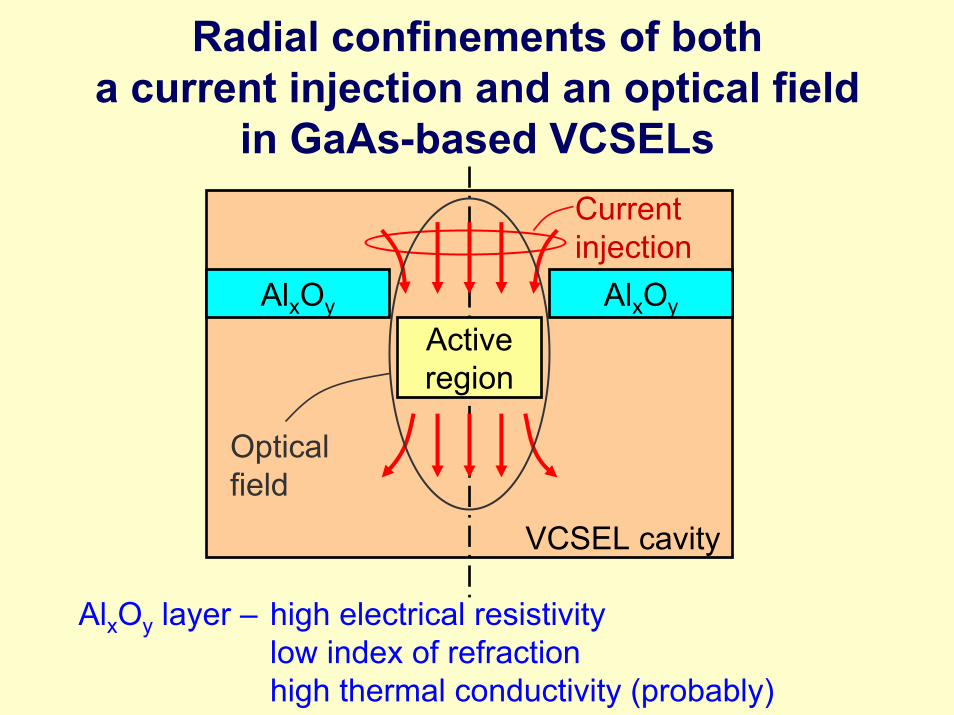
Radial confinements of botha current injection and an optical field
in GaAs-based VCSELs
VCSEL cavity
Activeregion
Currentinjection
AlxOy AlxOy
AlxOy layer – high electrical resistivitylow index of refractionhigh thermal conductivity (probably)
Opticalfield

Motivation
During the presentation, the designing strategy to enhance mode selectivity (i.e. to ensure the single fundamental
LP01 mode operation) in oxide-confined high-power VCSELs is presented.

The three-dimensional fullyself-consistent model
The model is composed of four interrelated parts: • the optical model describing for successive modes a
distribution of an optical field within the resonator and enabling determination of its lasing threshold,
• the electrical model characterizing both the current spreading between the top and bottom contacts and injection of carriers of both kinds into the active region,
• the thermal model characterizing generation of a heat flux and its spreading from heat sources towards heat sink and
• the gain model enabling determination of gain spectra within the active region.
R.P. Sarzała and W. Nakwaski, J. Phys.:Condens. Matter16 (2004) S3121-S3140

The calculation algorithmSTART
Room-temperaturecarrier-less values of all
model parameters
Determination of a 3D potential distribution
Set initial valueof applied voltage
Is theassumed exactness
achieved?
Determination of 3D temperature profiles
Is theassumed exactness
achieved?
Set new 3D profiles of all model
parameters
NO
YES
New effective conductivity of the
active region
NO
Determination of current injection into the active
region
Determination of the active-region gain spectra
Determination of 3D intensity profiles of successive
radiation modes
Is thelasing threshold
achieved?
STOP
Set a new value of an
applied voltage
YESNO
YES

VCSEL with a single oxide aperture
p-side DBRGaAs/Al0.8Ga0.2As
activeregion
oxidation
n-sideDBR
GaAs/AlAs
3 /2Resonator
p-sideDBR
Vertical Cavity SurfaceEmitting Laser
uppercontact
bottomcontact
activeregion
n-sideDBR
oxidation

The GaInNAs/GaAs 1.3-μm VCSEL witha single oxide aperture
The VCSEL structure is similar (but not identical) to the one reported by Infineon in A. Ramakrishnan et al., J. Cryst. Growth 248 (2003) 457
Layer
Thickness
nm
Refractiveindex
nR
RdndT
10-4/K
Group refractive
index nG
Absorptioncoefficient α
cm-1
ddTα
1/103cmK
GaAs upper DBR
28* 95.6 3.4 3.0 3.654 1 1.28
Al0.8Ga0.2As upper DBR
28* 108 3.01 1.47 3.198 1 1.28
p-GaAs 184.7 3.4 3.0 3.654 20 1.28 AlxOy 15 1.61 0 1.681 20 0
p-GaAs 165.2 3.4 3.0 3.654 5 1.28 Ga0.66In0.34N0.017As0.983
quantum well 2* 6.5 3.8 3.0 4.62 0 0
GaAs barrier
25 3.4 3.0 3.654 0 0
n-GaAs 171.6 3.4 3.0 3.654 2.5 1.28 GaAs
bottom DBR 34* 95.6 3.4 3.0 3.654 0.5 1.28
AlAs bottom DBR
34* 111.5 2.915 1.34 3.056 0.5 1.28

VCSEL with a single oxide apertureat the anti-node position

VCSEL with a single oxide apertureat the anti-node position
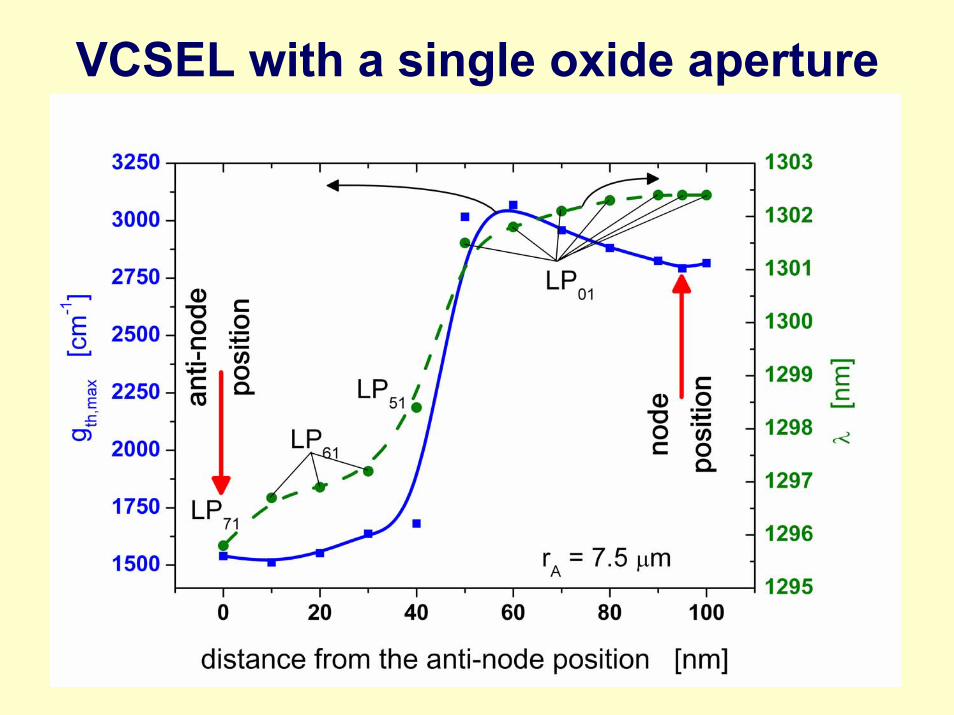
VCSEL with a single oxide aperture

VCSEL with a single oxide aperture
Number and
structure symbol
rA [μm]
Uth [V]
Ith [mA]
TA,max [K]
gth,max [cm-1]
mode λ [nm]
1 SN 10 3.65 21.13 316.83 4432 LP01 1303.22 SA 10 2.09 8.24 304.28 1644 LP11 1 1295.13 SN 7.5 2.55 10.22 308.16 2792 LP01 1302.44 SA 7.5 1.94 5.72 303.76 1539 LP71 1295.85 SN 5 1.99 5.11 305.18 2174 LP01 1302.16 SA 5 1.68 3.22 302.91 1311 LP31 1297.17 SN 2 2.75 4.85 315.68 6890 LP01 1302.38 SA 2 1.27 0.86 301.50 1189 LP01 1298.2

VCSEL with a single oxide aperture No further improvements are available in VCSELs with a single
oxide aperture. Then two extreme cases are possible: • Index-guided VCSELs: To reduce a VCSEL threshold
current, the radial index-guiding is necessary achieved with the aid of the oxide aperture located at the anti-node position of the resonator standing wave. But then, in the case of higher-output large-size VCSELs, higher-order transverse modes exhibit the lowest thresholds.
• Gain-guided VCSELs: To ensure the fundamental-mode LP01operation, the radial gain-guiding should be used realized in the VCSEL design with the oxide aperture located at the analogous node position. Then its threshold current is considerably higher.
Further improvements may be possible in VCSELs with two oxide apertures.

VCSEL with two oxide apertures

VCSEL with two oxide apertures
Layer
Thicknessnm
Refractiveindex
nR
RdndT
10-4/K
Group refractive
index nG
Absorptioncoefficient
α cm-1
ddTα
1/103cmK
GaAs upper DBR
28* 95.6 3.4 3.0 3.654 1 1.28
Al0.8Ga0.2As upper DBR
28* 108 3.01 1.47 3.198 1 1.28
p-GaAs 360.9 3.4 3.0 3.654 20 1.28 AlxOy 50 1.61 0 1.681 20 0
p-GaAs 341.2 3.4 3.0 3.654 5 1.28 Ga0.66In0.34N0.017As0.983
quantum well 2* 6.5 3.8 3.0 4.62 0 0
GaAs barrier
25 3.4 3.0 3.654 0 0
n-GaAs 260.5 3.4 3.0 3.654 2.5 1.28 AlxOy 15 1.61 0 1.681 2.5 0
n-GaAs 89.2 3.4 3.0 3.654 2.5 1.28 GaAs
bottom DBR 34* 95.6 3.4 3.0 3.654 0.5 1.28
AlAs bottom DBR
34* 111.5 2.915 1.34 3.056 0.5 1.28
The VCSEL structure is similar (but not identical) to the one reported by Infineon in A. Ramakrishnan et al., J. Cryst. Growth 248 (2003) 457

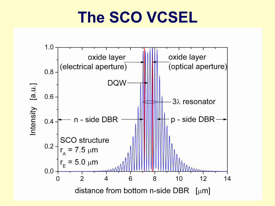
General strategy Much more improvements may be expected in the
oxide-confined VCSEL when: • one of its oxide apertures is localized in a VCSEL
cavity at the antinode position of the optical standing wave, where it is working as both the electrical aperture confining radially the current injection into the active region and the optical aperture introducing the built-in radial optical confinement mechanism,
• the second oxide aperture on the opposite side of the active region is shifted to the analogous standing-wave node position, where it is working as the electrical aperture only.

The SCO VCSEL – new conceptDiameters of both the apertures may be changed independently
giving an additional degree of freedom for VCSEL designing. Then the second aperture, located at the node position, will influence the current spreading only, whereas the first one, in the anti-node position, will mostly introduce the radial waveguiding effect. Both radial confinements influencing the current spreading and the electromagnetic field may be achieved separately, analogously to their axial confinements in the SCH (Separate Confinement Heterostructure) diode lasers. That is why we call this laser structure the SCO (Separate Confinement Oxidation) VCSEL.
Different aperture diameters may be obtained taking advantage of the dependence of radial oxidation kinetics on a composition and a thickness of the oxidized layer (see W. Nakwaski et al. Semicond. Sci. Technol. 19 (2004) 333)

Optical field
heterojunctions
carr
iers Optical field
current
oxid
e ap
ertu
res
SCOSeparateConfinementOxidation
SCHSeparateConfinementHeterostructure

The SCO VCSEL
DQW -GaInNAs/GaAs6.5 nm/25 nmactive region
oxide - opticalaperture
28 pairp-sideDBR
34 pair n-sideDBR
n - electrode
1300 nm
Heat Sink
p - electrode
3λ resonator
oxide - electricalaperture
SeparateConfinementOxidation
The SCO VCSEL

The SCO VCSEL
SCO

The SCO VCSEL
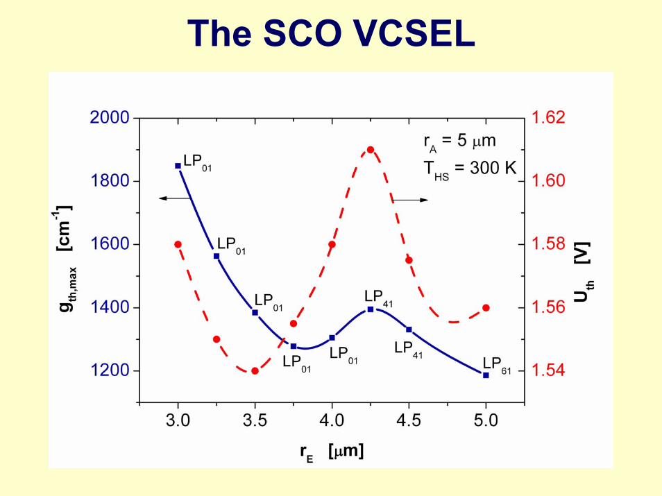
The SCO VCSEL

The SCO VCSEL
SCO

The SCO VCSELName of structure
rA [μm]
rE [μm]
Uth [V]
Ith [mA]
TA,max [K]
gth,max [cm-1]
MOD λ [nm]
1 SN 10 - 3.65 21.13 316.83 4432 LP01 1303.22 SCO 10 6 2.34 7.24 306.26 3128 LP01 1303.23 SA 10 - 2.09 8.24 304.28 1644 LP11 1 1295.14 SN 7.5 - 2.55 10.22 308.16 2792 LP01 1302.45 SCO 7.5 5 1.95 4.60 304.30 2094 LP01 1300.06 SA 7.5 - 1.94 5.72 303.76 1539 LP71 1295.87 SN 5 - 1.99 5.11 305.18 2174 LP01 1302.18 SCO 5 3.75 1.55 2.36 302.59 1518 LP01 1298.79 SA 5 - 1.68 3.22 302.91 1311 LP31 1297.110 SN 2 - 2.75 4.85 315.68 6890 LP01 1302.311 D 2 2 1.20 0.65 301.20 884 LP01 1296.612 SA 2 - 1.27 0.86 301.50 1189 LP01 1298.2
SN – single oxidation at the node position SA – single oxidation at the anti-node position D – two identical oxidations SCO – new SCO VCSEL
ConclusionsThe new SCO VCSEL structure demonstrates advantages of both the previous oxide-confinement VCSELs:• the stable single-fundamental-mode operation of the
gain-guided VCSEL with the oxide aperture located at the standing-wave node position, and
• the low lasing threshold of the index-guided VCSEL with the aperture shifted to the analogous anti-node position.
Therefore, the traditional VCSEL design with the oxide aperture located at the standing-wave node position may be recomended for the room-temperature operation of large-active-region VCSELs because of their relatively simple technology. In all other cases, the new SCO VCSEL structure ensures much better performance.