Control of power converter for grid integration of renewable energy conversion and STATCOM
energies
Article
A Multifunctional Isolated and Non-Isolated DualMode Converter for Renewable EnergyConversion Applications
Yiwang Wang 1,2,*, Chun Gan 3, Kai Ni 4 ID , Xinhua Li 4, Houjun Tang 1 and Yong Yang 5
1 Department of Electrical Engineering, Shanghai Jiao Tong University, Shanghai 200240, China;[email protected]
2 School of Electronic and Information Engineering, Suzhou Vocational University, Suzhou 215104, China3 Department of Electrical Engineering and Computer Science, University of Tennessee,
Knoxville, TN 37996, USA; [email protected] Department of Electrical Engineering and Electronics, University of Liverpool, Liverpool L69 3GJ, UK;
[email protected] (K.N.); [email protected] (X.L.)5 School of Urban Rail Transportation, Soochow University, Suzhou 215137, China; [email protected]* Correspondence: [email protected]; Tel.: +86-158-5018-3606
Received: 16 October 2017; Accepted: 25 November 2017; Published: 30 November 2017
Abstract: In this paper, a multifunctional isolated and non-isolated dual-mode low-power converterwas designed for renewable energy conversion applications such as photovoltaic power generationto achieve different operating modes under bi-directional electrical conversion. The proposedtopology consists of a bidirectional non-isolated DC/DC circuit and an isolated converter with ahigh-frequency transformer, which merge the advantages of both the conventional isolated converterand non-isolated converter with the combination of the two converter technologies. Compared withtraditional converters, the multifunctional converter can not only realize conventional bi-directionalfunctions, but can also be applied for many different operation modes and meet the high output/inputratio demands with the two converter circuits operating together. A novel control algorithm wasproposed to achieve the various functions of the proposed converter. An experimental platform basedon the proposed circuit was established. Both the simulation and experimental results indicatedthat the proposed converter could provide isolated and non-isolated modes in different applications,which could meet different practical engineering requirements.
Keywords: multifunctional converter; bi-directional; isolated and non-isolated; dual mode; control
1. Introduction
With the development of power electronics, solid state converters have been widely used in severalrenewable energy applications [1–6]. Different applications require different converter topologies,which can be divided into isolated and non-isolated converters. In recent years, with further renewableenergy systems, new requirements for power electronic conversion have been proposed.
Currently, there are some converter topologies for solar power and other renewable energyapplications [6–9]. Generally, the grid-connected systems use non-isolated converters in mostconditions. In some distributed power generators, a single-phase two-stage transformerless circuit isusually used, and the converter can be used to step up the DC voltage [10] in the similar way to boostand buck-boost converters [11]. These topologies are suitable for grid-connected applications withhigh efficiency, low cost, and compact structures [12,13]. However, in stand-alone system applications,isolated converters or inverters are mostly employed in the power conversion circuits [14–19].
In [20], a power system using a high step-up converter for dc load applications in a photovoltaicenergy conversion system was presented. The developed converter adopted a coupled inductor
Energies 2017, 10, 1980; doi:10.3390/en10121980 www.mdpi.com/journal/energies
Energies 2017, 10, 1980 2 of 17
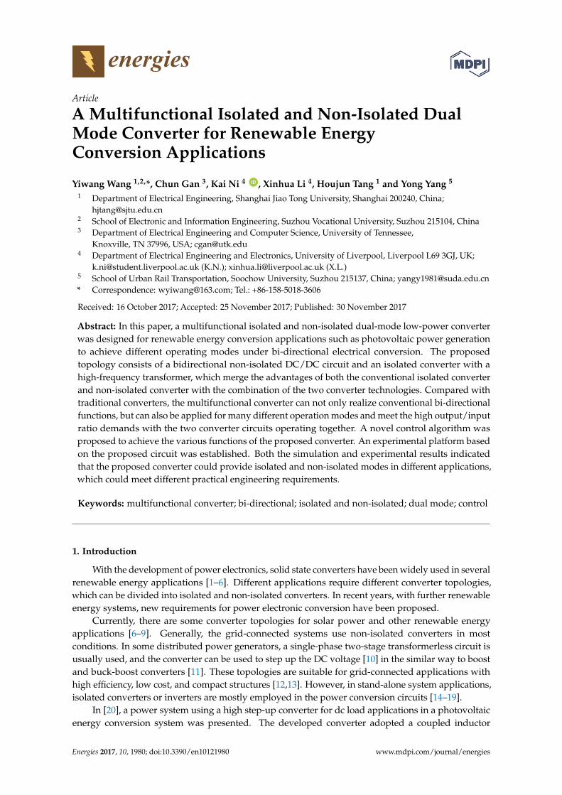
and a boost converter working in interleaved mode. A novel high step-up DC-DC converter wassuccessfully integrated using a coupled inductor and the switched capacitor techniques described in [21].Nevertheless, these converters only control the power flow from the input array to loads in a uniquedirection or could not achieve galvanic isolation applications. With the emergence of new energyapplications, compared with the single-function of a grid-connected or off-grid (stand-alone) system,new dual-mode [22,23] or multifunctional applications [24,25] have become more popular, which area new trend in the future for renewable energy applications [19]. As different conversion modes arerequired in different applications, more flexible and reliable conversion circuits are needed. This paperproposes a new multifunctional isolated and non-isolated dual mode low-power converter, and showsa block diagram of the proposed converter system is shown in Figure 1.
Energies 2017, 10, 1980 2 of 17
applications, isolated converters or inverters are mostly employed in the power conversion circuits
[14–19].
In [20], a power system using a high step-up converter for dc load applications in a photovoltaic
energy conversion system was presented. The developed converter adopted a coupled inductor and
a boost converter working in interleaved mode. A novel high step-up DC-DC converter was
successfully integrated using a coupled inductor and the switched capacitor techniques described in
[21]. Nevertheless, these converters only control the power flow from the input array to loads in a
unique direction or could not achieve galvanic isolation applications. With the emergence of new
energy applications, compared with the single-function of a grid-connected or off-grid (stand-alone)
system, new dual-mode [22,23] or multifunctional applications [24,25] have become more popular,
which are a new trend in the future for renewable energy applications [19]. As different conversion
modes are required in different applications, more flexible and reliable conversion circuits are needed.
This paper proposes a new multifunctional isolated and non-isolated dual mode low-power
converter, and shows a block diagram of the proposed converter system is shown in Figure 1.
Figure 1. Block diagram of the proposed converter application system.
Compared to traditional converters, with the addition of the realization of conventional
bi-directional function, the multifunctional converter can also be applied for both the isolated and
non-isolated operation modes. Switching between the isolated and non-isolated operation modes is
presented according to different applications by adjusting the control switch signals, which are
flexible to change in the operation mode for renewable energy conversion applications. The
simulation and experimental results indicated that the proposed topology could provide an efficient
isolated or non-isolated dual mode converter under different applications and meet the different
practical engineering requirements.
The paper is organized as follows: Section 2 describes the topology of the proposed
multifunctional converter. Different operation modes and control strategies are explained in Section 3.
Section 4 introduces the design of key parameters for the proposed converter. In Section 5, the
simulation tests and experimental results are displayed and discussed. Finally, the conclusions are
presented in Section 6.
2. Proposed Multifunctional Isolated and Non-Isolated Dual Mode Converter
The single bidirectional buck/boost non-isolated converter or flyback isolated converter is a
DC/DC electrical power conversion solution for grid-connected or stand-alone energy system
projects due to their technical maturity. The flyback converter has been widely used in a large number
of power conversions due to its relatively simple structure, good performance, and galvanic isolation
[26–28]. A bidirectional buck/boost converter is a mature topology in power electronics systems due
to its simplicity and high efficiency [29]; however, the conventional buck/boost converter cannot
Bidirectional
DC/DC
Converter
DC/AC
Inverter
Renewable
Energy
Source
Utility
LoadsLocaloutput
Grid-
Connected
Stand-
alone
Proposed Multifunctional
Isolated and Non-isolated
Dual Mode Converter
Solar PV
array
Wind &
other
Storge energy
Battery
A B
Figure 1. Block diagram of the proposed converter application system.
Compared to traditional converters, with the addition of the realization of conventionalbi-directional function, the multifunctional converter can also be applied for both the isolated andnon-isolated operation modes. Switching between the isolated and non-isolated operation modesis presented according to different applications by adjusting the control switch signals, which areflexible to change in the operation mode for renewable energy conversion applications. The simulationand experimental results indicated that the proposed topology could provide an efficient isolatedor non-isolated dual mode converter under different applications and meet the different practicalengineering requirements.
The paper is organized as follows: Section 2 describes the topology of the proposed multifunctionalconverter. Different operation modes and control strategies are explained in Section 3. Section 4introduces the design of key parameters for the proposed converter. In Section 5, the simulationtests and experimental results are displayed and discussed. Finally, the conclusions are presented inSection 6.
2. Proposed Multifunctional Isolated and Non-Isolated Dual Mode Converter
The single bidirectional buck/boost non-isolated converter or flyback isolated converter is aDC/DC electrical power conversion solution for grid-connected or stand-alone energy system projectsdue to their technical maturity. The flyback converter has been widely used in a large number of powerconversions due to its relatively simple structure, good performance, and galvanic isolation [26–28].A bidirectional buck/boost converter is a mature topology in power electronics systems due to itssimplicity and high efficiency [29]; however, the conventional buck/boost converter cannot achieveinput and output galvanic isolation. To simultaneously implement the functions of isolated andnon-isolated converters and benefit from the advantages of the two converter circuits, this paperproposes a novel multifunctional isolated and non-isolated dual mode converter by increasing the
Energies 2017, 10, 1980 3 of 17
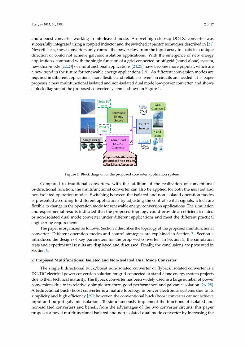
control transfer units. The design methodology of the proposed new converter is depicted in Figure 2.Since the conventional bidirectional buck/boost converter and flyback converters are complementaryin galvanic and other technical characteristics, it is feasible and reasonable to combine them to createa new multifunctional isolated/non-isolated dual mode converter where the buck/boost converteroperates in the non-isolated operation mode and the flyback converter operates in the isolated operationmode. The new converter contains a non-isolated bidirectional step-up and step-down front-stagecircuit, an isolated converter, and a conversion control switching circuit. By adjusting the controllabledevices and transfer switches, the different operation modes can be interchanged.
Energies 2017, 10, 1980 3 of 17
achieve input and output galvanic isolation. To simultaneously implement the functions of isolated
and non-isolated converters and benefit from the advantages of the two converter circuits, this paper
proposes a novel multifunctional isolated and non-isolated dual mode converter by increasing the
control transfer units. The design methodology of the proposed new converter is depicted in Figure 2.
Since the conventional bidirectional buck/boost converter and flyback converters are complementary
in galvanic and other technical characteristics, it is feasible and reasonable to combine them to create
a new multifunctional isolated/non-isolated dual mode converter where the buck/boost converter
operates in the non-isolated operation mode and the flyback converter operates in the isolated
operation mode. The new converter contains a non-isolated bidirectional step-up and step-down
front-stage circuit, an isolated converter, and a conversion control switching circuit. By adjusting the
controllable devices and transfer switches, the different operation modes can be interchanged.
Conventional
Bidirectional
DC/DC Converter
Characteristic:
Simple structure, High efficieny,
Easy to implement
Bidirectional
Flyback Converter
Characteristic:
Low cost, Galvanic isolation
Engineering
application
requirement
Different operation mode need
different converter
Modified
converter structureProposed
multifunctional isolated
and non-isolated dual
mode topology
Figure 2. The design methodology of proposed new converter.
The schematic of the proposed converter is illustrated in Figure 2. It consists of a bidirectional
non-isolated conventional DC/DC circuit and an isolated converter with a high-frequency
transformer, and these two parts are connected by the transfer switches. A common buck/boost bi-
directional converter is employed as the non-isolated stage converter including a conventional non-
isolated bidirectional step-up and step-down circuit in the proposed topology. The isolated stage
converter is composed of a bidirectional flyback converter.
The proposed circuit schematic is shown in Figure 3, where U1 and U2 denote the port1 (DC bus
or U1 side) voltage and the port2 (storage system or U2 side) voltage, respectively. S1 (D1), S2 (D2), Si1
(Di1), and Si2 (D2) are fully-controlled power electronic switching devices in the converter; Si1 and Si2
are the switches in the isolated converter; C1 and C2 are the non-isolated converter capacitors; C3
represents the filter capacitor; L is the inductor of a non-isolated converter; and T is the isolated stage
converter flyback transformer.
T
U1
++
A
B
K1
K2
S1
S2Si2Si1
Di1
Di2
C1 C2C3
LD1
D2
Non-isolated stage converter Isolated stage converter
Power flow
U2
Figure 3. Proposed multifunctional bidirectional dual-mode converter.
The proposed new dual-mode converter merges the advantages of both the conventional
isolated converter and non-isolated converter to create a blend of two types of converter technologies.
The new converter not only copes with the common function requirements, but also meets the high
output/input ratio demands when the two converter circuits operate together.
Figure 2. The design methodology of proposed new converter.
The schematic of the proposed converter is illustrated in Figure 2. It consists of a bidirectionalnon-isolated conventional DC/DC circuit and an isolated converter with a high-frequency transformer,and these two parts are connected by the transfer switches. A common buck/boost bi-directionalconverter is employed as the non-isolated stage converter including a conventional non-isolatedbidirectional step-up and step-down circuit in the proposed topology. The isolated stage converter iscomposed of a bidirectional flyback converter.
The proposed circuit schematic is shown in Figure 3, where U1 and U2 denote the port1 (DCbus or U1 side) voltage and the port2 (storage system or U2 side) voltage, respectively. S1 (D1),S2 (D2), Si1 (Di1), and Si2 (D2) are fully-controlled power electronic switching devices in the converter;Si1 and Si2 are the switches in the isolated converter; C1 and C2 are the non-isolated converter capacitors;C3 represents the filter capacitor; L is the inductor of a non-isolated converter; and T is the isolatedstage converter flyback transformer.
Energies 2017, 10, 1980 3 of 17
achieve input and output galvanic isolation. To simultaneously implement the functions of isolated
and non-isolated converters and benefit from the advantages of the two converter circuits, this paper
proposes a novel multifunctional isolated and non-isolated dual mode converter by increasing the
control transfer units. The design methodology of the proposed new converter is depicted in Figure 2.
Since the conventional bidirectional buck/boost converter and flyback converters are complementary
in galvanic and other technical characteristics, it is feasible and reasonable to combine them to create
a new multifunctional isolated/non-isolated dual mode converter where the buck/boost converter
operates in the non-isolated operation mode and the flyback converter operates in the isolated
operation mode. The new converter contains a non-isolated bidirectional step-up and step-down
front-stage circuit, an isolated converter, and a conversion control switching circuit. By adjusting the
controllable devices and transfer switches, the different operation modes can be interchanged.
Conventional
Bidirectional
DC/DC Converter
Characteristic:
Simple structure, High efficieny,
Easy to implement
Bidirectional
Flyback Converter
Characteristic:
Low cost, Galvanic isolation
Engineering
application
requirement
Different operation mode need
different converter
Modified
converter structureProposed
multifunctional isolated
and non-isolated dual
mode topology
Figure 2. The design methodology of proposed new converter.
The schematic of the proposed converter is illustrated in Figure 2. It consists of a bidirectional
non-isolated conventional DC/DC circuit and an isolated converter with a high-frequency
transformer, and these two parts are connected by the transfer switches. A common buck/boost bi-
directional converter is employed as the non-isolated stage converter including a conventional non-
isolated bidirectional step-up and step-down circuit in the proposed topology. The isolated stage
converter is composed of a bidirectional flyback converter.
The proposed circuit schematic is shown in Figure 3, where U1 and U2 denote the port1 (DC bus
or U1 side) voltage and the port2 (storage system or U2 side) voltage, respectively. S1 (D1), S2 (D2), Si1
(Di1), and Si2 (D2) are fully-controlled power electronic switching devices in the converter; Si1 and Si2
are the switches in the isolated converter; C1 and C2 are the non-isolated converter capacitors; C3
represents the filter capacitor; L is the inductor of a non-isolated converter; and T is the isolated stage
converter flyback transformer.
T
U1
++
A
B
K1
K2
S1
S2Si2Si1
Di1
Di2
C1 C2C3
LD1
D2
Non-isolated stage converter Isolated stage converter
Power flow
U2
Figure 3. Proposed multifunctional bidirectional dual-mode converter.
The proposed new dual-mode converter merges the advantages of both the conventional
isolated converter and non-isolated converter to create a blend of two types of converter technologies.
The new converter not only copes with the common function requirements, but also meets the high
output/input ratio demands when the two converter circuits operate together.
Figure 3. Proposed multifunctional bidirectional dual-mode converter.
The proposed new dual-mode converter merges the advantages of both the conventional isolatedconverter and non-isolated converter to create a blend of two types of converter technologies. The newconverter not only copes with the common function requirements, but also meets the high output/inputratio demands when the two converter circuits operate together.
Energies 2017, 10, 1980 4 of 17
As previously depicted, the proposed new converter topology is an integrated conventionalbidirectional buck/boost circuit and a bidirectional flyback circuit. The novel converter works in twodifferent modes.
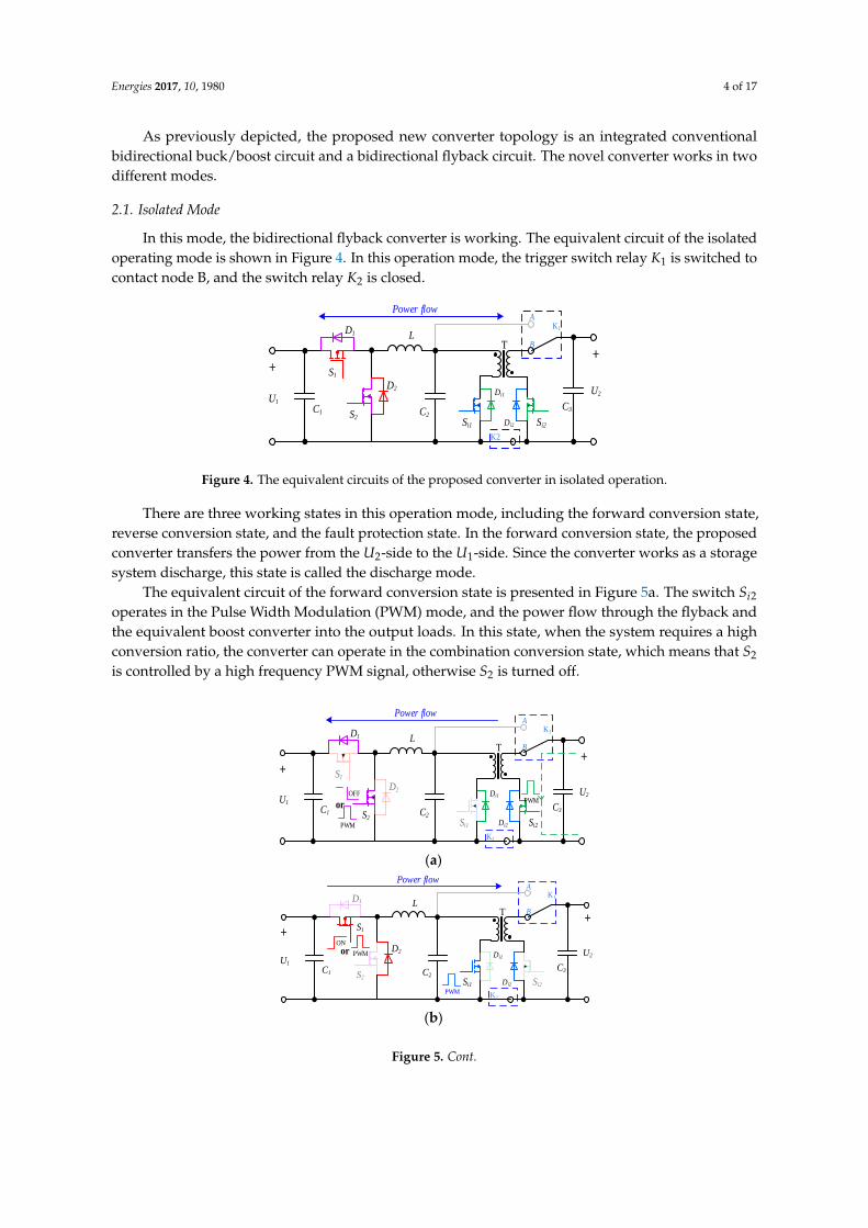
2.1. Isolated Mode
In this mode, the bidirectional flyback converter is working. The equivalent circuit of the isolatedoperating mode is shown in Figure 4. In this operation mode, the trigger switch relay K1 is switched tocontact node B, and the switch relay K2 is closed.
Energies 2017, 10, 1980 4 of 17
As previously depicted, the proposed new converter topology is an integrated conventional
bidirectional buck/boost circuit and a bidirectional flyback circuit. The novel converter works in two
different modes.
2.1. Isolated Mode
In this mode, the bidirectional flyback converter is working. The equivalent circuit of the isolated
operating mode is shown in Figure 4. In this operation mode, the trigger switch relay K1 is switched
to contact node B, and the switch relay K2 is closed.
T
U1
++
A
B
K1
K2
S1
S2Si2Si1
Di1
Di2
C1 C2C3
LD1
D2
Power flow
U2
Figure 4. The equivalent circuits of the proposed converter in isolated operation.
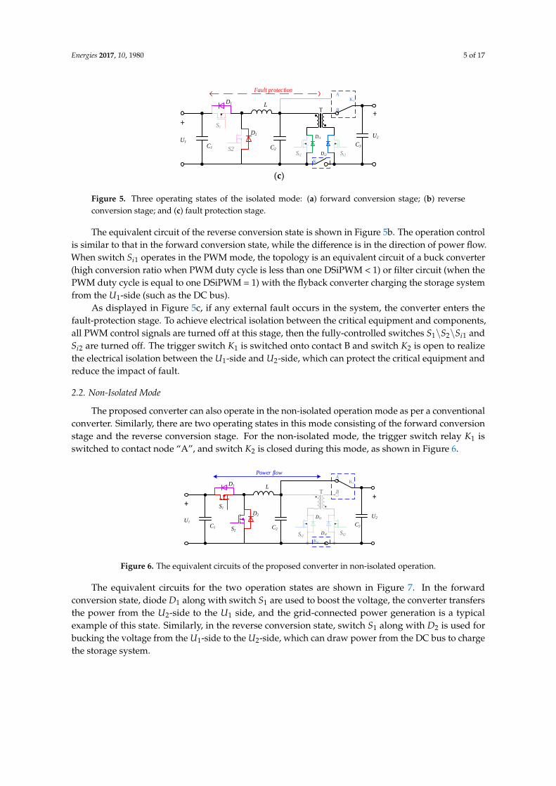
There are three working states in this operation mode, including the forward conversion state,
reverse conversion state, and the fault protection state. In the forward conversion state, the proposed
converter transfers the power from the U2-side to the U1-side. Since the converter works as a storage
system discharge, this state is called the discharge mode.
The equivalent circuit of the forward conversion state is presented in Figure 5a. The switch Si2
operates in the Pulse Width Modulation (PWM) mode, and the power flow through the flyback and
the equivalent boost converter into the output loads. In this state, when the system requires a high
conversion ratio, the converter can operate in the combination conversion state, which means that S2
is controlled by a high frequency PWM signal, otherwise S2 is turned off.
The equivalent circuit of the reverse conversion state is shown in Figure 5b. The operation
control is similar to that in the forward conversion state, while the difference is in the direction of
power flow. When switch Si1 operates in the PWM mode, the topology is an equivalent circuit of a
buck converter (high conversion ratio when PWM duty cycle is less than one DSiPWM < 1) or filter
circuit (when the PWM duty cycle is equal to one DSiPWM = 1) with the flyback converter charging
the storage system from the U1-side (such as the DC bus).
+
U2
T
U1
+
A
B
K1
K2
S1
S2Si2Si1
Di1
Di2
C1 C2C3
LD1
D2
Power flow
PWM
PWMOFF
or
(a)
U1
+
T
A
B
K1
K2
S1
S2Si2Si1
Di1
Di2
C1 C2C3
LD1
D2
Power flow
PWM
PWM
+
ON
or U2
(b)
Figure 4. The equivalent circuits of the proposed converter in isolated operation.
There are three working states in this operation mode, including the forward conversion state,reverse conversion state, and the fault protection state. In the forward conversion state, the proposedconverter transfers the power from the U2-side to the U1-side. Since the converter works as a storagesystem discharge, this state is called the discharge mode.
The equivalent circuit of the forward conversion state is presented in Figure 5a. The switch Si2operates in the Pulse Width Modulation (PWM) mode, and the power flow through the flyback andthe equivalent boost converter into the output loads. In this state, when the system requires a highconversion ratio, the converter can operate in the combination conversion state, which means that S2
is controlled by a high frequency PWM signal, otherwise S2 is turned off.
Energies 2017, 10, 1980 4 of 17
As previously depicted, the proposed new converter topology is an integrated conventional
bidirectional buck/boost circuit and a bidirectional flyback circuit. The novel converter works in two
different modes.
2.1. Isolated Mode
In this mode, the bidirectional flyback converter is working. The equivalent circuit of the isolated
operating mode is shown in Figure 4. In this operation mode, the trigger switch relay K1 is switched
to contact node B, and the switch relay K2 is closed.
T
U1
++
A
B
K1
K2
S1
S2Si2Si1
Di1
Di2
C1 C2C3
LD1
D2
Power flow
U2
Figure 4. The equivalent circuits of the proposed converter in isolated operation.
There are three working states in this operation mode, including the forward conversion state,
reverse conversion state, and the fault protection state. In the forward conversion state, the proposed
converter transfers the power from the U2-side to the U1-side. Since the converter works as a storage
system discharge, this state is called the discharge mode.
The equivalent circuit of the forward conversion state is presented in Figure 5a. The switch Si2
operates in the Pulse Width Modulation (PWM) mode, and the power flow through the flyback and
the equivalent boost converter into the output loads. In this state, when the system requires a high
conversion ratio, the converter can operate in the combination conversion state, which means that S2
is controlled by a high frequency PWM signal, otherwise S2 is turned off.
The equivalent circuit of the reverse conversion state is shown in Figure 5b. The operation
control is similar to that in the forward conversion state, while the difference is in the direction of
power flow. When switch Si1 operates in the PWM mode, the topology is an equivalent circuit of a
buck converter (high conversion ratio when PWM duty cycle is less than one DSiPWM < 1) or filter
circuit (when the PWM duty cycle is equal to one DSiPWM = 1) with the flyback converter charging
the storage system from the U1-side (such as the DC bus).
+
U2
T
U1
+
A
B
K1
K2
S1
S2Si2Si1
Di1
Di2
C1 C2C3
LD1
D2
Power flow
PWM
PWMOFF
or
(a)
U1
+
T
A
B
K1
K2
S1
S2Si2Si1
Di1
Di2
C1 C2C3
LD1
D2
Power flow
PWM
PWM
+
ON
or U2
(b)
Figure 5. Cont.
Energies 2017, 10, 1980 5 of 17
Energies 2017, 10, 1980 5 of 17
U2U1
+
T
A
B
K1
K2
S1
S2Si2Si1
Di1
Di2
C1 C2C3
LD1
D2
Fault protection
+
(c)
Figure 5. Three operating states of the isolated mode: (a) forward conversion stage; (b) reverse
conversion stage; and (c) fault protection stage.
As displayed in Figure 5c, if any external fault occurs in the system, the converter enters the
fault-protection stage. To achieve electrical isolation between the critical equipment and components,
all PWM control signals are turned off at this stage, then the fully-controlled switches S1\S2\Si1 and
Si2 are turned off. The trigger switch K1 is switched onto contact B and switch K2 is open to realize the
electrical isolation between the U1-side and U2-side, which can protect the critical equipment and
reduce the impact of fault.
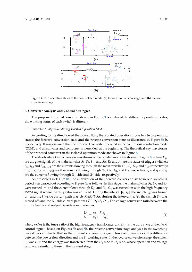
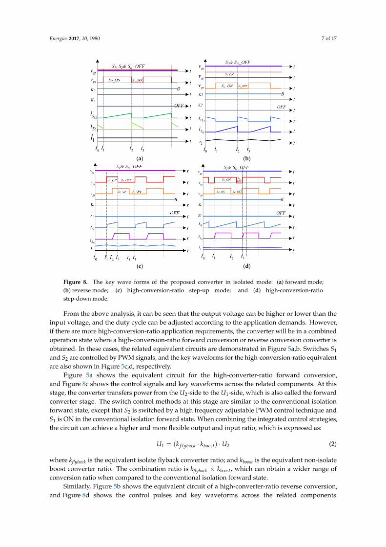
2.2. Non-Isolated Mode
The proposed converter can also operate in the non-isolated operation mode as per a
conventional converter. Similarly, there are two operating states in this mode consisting of the
forward conversion stage and the reverse conversion stage. For the non-isolated mode, the trigger
switch relay K1 is switched to contact node “A”, and switch K2 is closed during this mode, as shown
in Figure 6.
T
U1
++
A
B
K1
K2
S1
S2Si2Si1
Di1
Di2
C1 C2C3
LD1
D2
Power flow
U2
Figure 6. The equivalent circuits of the proposed converter in non-isolated operation.
T
U1
++
A
B
K1
K2
S1
S2Si2Si1
Di1
Di2
C1 C2C3
LD1
D2
Power flow
U2
PWM
(a)
T
U1
++
A
B
K1
K2
S1
S2Si2Si1
Di1
Di2
C1 C2C3
LD1
D2
Power flow
U2
(b)
Figure 7. Two operating states of the non-isolated mode: (a) forward conversion stage; and (b) reverse
conversion stage.
Figure 5. Three operating states of the isolated mode: (a) forward conversion stage; (b) reverseconversion stage; and (c) fault protection stage.
The equivalent circuit of the reverse conversion state is shown in Figure 5b. The operation controlis similar to that in the forward conversion state, while the difference is in the direction of power flow.When switch Si1 operates in the PWM mode, the topology is an equivalent circuit of a buck converter(high conversion ratio when PWM duty cycle is less than one DSiPWM < 1) or filter circuit (when thePWM duty cycle is equal to one DSiPWM = 1) with the flyback converter charging the storage systemfrom the U1-side (such as the DC bus).
As displayed in Figure 5c, if any external fault occurs in the system, the converter enters thefault-protection stage. To achieve electrical isolation between the critical equipment and components,all PWM control signals are turned off at this stage, then the fully-controlled switches S1\S2\Si1 andSi2 are turned off. The trigger switch K1 is switched onto contact B and switch K2 is open to realizethe electrical isolation between the U1-side and U2-side, which can protect the critical equipment andreduce the impact of fault.
2.2. Non-Isolated Mode
The proposed converter can also operate in the non-isolated operation mode as per a conventionalconverter. Similarly, there are two operating states in this mode consisting of the forward conversionstage and the reverse conversion stage. For the non-isolated mode, the trigger switch relay K1 isswitched to contact node “A”, and switch K2 is closed during this mode, as shown in Figure 6.
Energies 2017, 10, 1980 5 of 17
U2U1
+
T
A
B
K1
K2
S1
S2Si2Si1
Di1
Di2
C1 C2C3
LD1
D2
Fault protection
+
(c)
Figure 5. Three operating states of the isolated mode: (a) forward conversion stage; (b) reverse
conversion stage; and (c) fault protection stage.
As displayed in Figure 5c, if any external fault occurs in the system, the converter enters the
fault-protection stage. To achieve electrical isolation between the critical equipment and components,
all PWM control signals are turned off at this stage, then the fully-controlled switches S1\S2\Si1 and
Si2 are turned off. The trigger switch K1 is switched onto contact B and switch K2 is open to realize the
electrical isolation between the U1-side and U2-side, which can protect the critical equipment and
reduce the impact of fault.
2.2. Non-Isolated Mode
The proposed converter can also operate in the non-isolated operation mode as per a
conventional converter. Similarly, there are two operating states in this mode consisting of the
forward conversion stage and the reverse conversion stage. For the non-isolated mode, the trigger
switch relay K1 is switched to contact node “A”, and switch K2 is closed during this mode, as shown
in Figure 6.
T
U1
++
A
B
K1
K2
S1
S2Si2Si1
Di1
Di2
C1 C2C3
LD1
D2
Power flow
U2
Figure 6. The equivalent circuits of the proposed converter in non-isolated operation.
T
U1
++
A
B
K1
K2
S1
S2Si2Si1
Di1
Di2
C1 C2C3
LD1
D2
Power flow
U2
PWM
(a)
T
U1
++
A
B
K1
K2
S1
S2Si2Si1
Di1
Di2
C1 C2C3
LD1
D2
Power flow
U2
(b)
Figure 7. Two operating states of the non-isolated mode: (a) forward conversion stage; and (b) reverse
conversion stage.
Figure 6. The equivalent circuits of the proposed converter in non-isolated operation.
The equivalent circuits for the two operation states are shown in Figure 7. In the forwardconversion state, diode D1 along with switch S1 are used to boost the voltage, the converter transfersthe power from the U2-side to the U1 side, and the grid-connected power generation is a typicalexample of this state. Similarly, in the reverse conversion state, switch S1 along with D2 is used forbucking the voltage from the U1-side to the U2-side, which can draw power from the DC bus to chargethe storage system.
Energies 2017, 10, 1980 6 of 17
Energies 2017, 10, 1980 5 of 17
U2U1
+
T
A
B
K1
K2
S1
S2Si2Si1
Di1
Di2
C1 C2C3
LD1
D2
Fault protection
+
(c)
Figure 5. Three operating states of the isolated mode: (a) forward conversion stage; (b) reverse
conversion stage; and (c) fault protection stage.
As displayed in Figure 5c, if any external fault occurs in the system, the converter enters the
fault-protection stage. To achieve electrical isolation between the critical equipment and components,
all PWM control signals are turned off at this stage, then the fully-controlled switches S1\S2\Si1 and
Si2 are turned off. The trigger switch K1 is switched onto contact B and switch K2 is open to realize the
electrical isolation between the U1-side and U2-side, which can protect the critical equipment and
reduce the impact of fault.
2.2. Non-Isolated Mode
The proposed converter can also operate in the non-isolated operation mode as per a
conventional converter. Similarly, there are two operating states in this mode consisting of the
forward conversion stage and the reverse conversion stage. For the non-isolated mode, the trigger
switch relay K1 is switched to contact node “A”, and switch K2 is closed during this mode, as shown
in Figure 6.
T
U1
++
A
B
K1
K2
S1
S2Si2Si1
Di1
Di2
C1 C2C3
LD1
D2
Power flow
U2
Figure 6. The equivalent circuits of the proposed converter in non-isolated operation.
T
U1
++
A
B
K1
K2
S1
S2Si2Si1
Di1
Di2
C1 C2C3
LD1
D2
Power flow
U2
PWM
(a)
T
U1
++
A
B
K1
K2
S1
S2Si2Si1
Di1
Di2
C1 C2C3
LD1
D2
Power flow
U2
(b)
Figure 7. Two operating states of the non-isolated mode: (a) forward conversion stage; and (b) reverse
conversion stage. Figure 7. Two operating states of the non-isolated mode: (a) forward conversion stage; and (b) reverseconversion stage.
3. Converter Analysis and Control Strategies
The proposed original converter shown in Figure 3 is analyzed. In different operating modes,the working status of each switch is different.
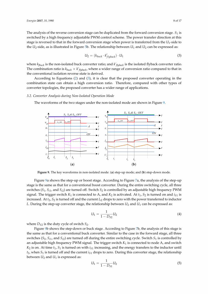
3.1. Converter Analyzation during Isolated Operation Mode
According to the direction of the power flow, the isolated operation mode has two operatingstates: the forward conversion state and the reverse conversion state as illustrated in Figure 5a,b,respectively. It was assumed that the proposed converter operated in the continuous conduction mode(CCM), and all switches and components were ideal at the beginning. The theoretical key waveformsof the proposed converter in the isolated operation mode are shown in Figure 8.
The steady-state key conversion waveforms of the isolated mode are shown in Figure 8, where Vgs
are the gate signals of the main switches S1, S2, Si1, and Si2; K1 and K2 are the states of trigger switches;iS1, iS2 and iSi1, iSi2 are the currents flowing through the main switches S1, S2, Si1, and Si2, respectively;iD1, iD2, iDi1, and iDi1 are the currents flowing through D1, D2, Di1, and Di2, respectively; and i1 and i2are the currents flowing through U1-side and U2-side, respectively.
As presented in Figure 8a, the analyzation of the forward conversion stage in one switchingperiod was carried out according to Figure 5a as follows: In this stage, the main switches S1, S2, and Si1were turned off, and the current flows through Di1 and D1; Si1 was turned on with the high frequencyPWM signal where the duty ratio was adjusted. During the interval [t1, t2], the switch Si2 was turnedon, and the U2-side current path was U2-K1(B)-T-Si2; during the interval [t3, t4], the switch Si2 wasturned off, and the U1-side current path was T-L-D1-U1-Di1. The voltage conversion ratio between theinput U2-side and output U1-side is expressed as:
U2
U1=
n2
n1
DSi2
1− DSi2
(1)
where n2/n1 is the turns ratio of the high frequency transformer; and Dsi1 is the duty cycle of the PWMcontrol signal. Based on Figures 5b and 8b, the reverse conversion stage analysis in the switchingperiod was similar to that in the forward conversion stage. However, there was still a differencebetween the power flow direction and the S1 working state. In the reverse conversion stage, the switchS1 was OFF and the energy was transferred from the U1-side to U2-side, whose operation and voltageratio were similar to those in the forward stage.
Energies 2017, 10, 1980 7 of 17
Energies 2017, 10, 1980 6 of 17
The equivalent circuits for the two operation states are shown in Figure 7. In the forward
conversion state, diode D1 along with switch S1 are used to boost the voltage, the converter transfers
the power from the U2-side to the U1 side, and the grid-connected power generation is a typical
example of this state. Similarly, in the reverse conversion state, switch S1 along with D2 is used for
bucking the voltage from the U1-side to the U2-side, which can draw power from the DC bus to charge
the storage system.
3. Converter Analysis and Control Strategies
The proposed original converter shown in Figure 3 is analyzed. In different operating modes,
the working status of each switch is different.
3.1. Converter Analyzation during Isolated Operation Mode
According to the direction of the power flow, the isolated operation mode has two operating
states: the forward conversion state and the reverse conversion state as illustrated in Figure 5a,b,
respectively. It was assumed that the proposed converter operated in the continuous conduction
mode (CCM), and all switches and components were ideal at the beginning. The theoretical key
waveforms of the proposed converter in the isolated operation mode are shown in Figure 8.
(a) (b)
(c) (d)
Figure 8. The key wave forms of the proposed converter in isolated mode: (a) forward mode; (b)
reverse mode; (c) high-conversion-ratio step-up mode; and (d) high-conversion-ratio step-down
mode.
The steady-state key conversion waveforms of the isolated mode are shown in Figure 8, where
Vgs are the gate signals of the main switches S1, S2, Si1, and Si2; K1 and K2 are the states of trigger
Figure 8. The key wave forms of the proposed converter in isolated mode: (a) forward mode;(b) reverse mode; (c) high-conversion-ratio step-up mode; and (d) high-conversion-ratiostep-down mode.
From the above analysis, it can be seen that the output voltage can be higher or lower than theinput voltage, and the duty cycle can be adjusted according to the application demands. However,if there are more high-conversion-ratio application requirements, the converter will be in a combinedoperation state where a high-conversion-ratio forward conversion or reverse conversion converter isobtained. In these cases, the related equivalent circuits are demonstrated in Figure 5a,b. Switches S1
and S2 are controlled by PWM signals, and the key waveforms for the high-conversion-ratio equivalentare also shown in Figure 5c,d, respectively.
Figure 5a shows the equivalent circuit for the high-converter-ratio forward conversion,and Figure 8c shows the control signals and key waveforms across the related components. At thisstage, the converter transfers power from the U2-side to the U1-side, which is also called the forwardconverter stage. The switch control methods at this stage are similar to the conventional isolationforward state, except that S2 is switched by a high frequency adjustable PWM control technique andS1 is ON in the conventional isolation forward state. When combining the integrated control strategies,the circuit can achieve a higher and more flexible output and input ratio, which is expressed as:
U1 = (k f lyback · kboost) ·U2 (2)
where kflyback is the equivalent isolate flyback converter ratio; and kboost is the equivalent non-isolateboost converter ratio. The combination ratio is kflyback × kboost, which can obtain a wider range ofconversion ratio when compared to the conventional isolation forward state.
Similarly, Figure 5b shows the equivalent circuit of a high-converter-ratio reverse conversion,and Figure 8d shows the control pulses and key waveforms across the related components.
Energies 2017, 10, 1980 8 of 17
The analysis of the reverse conversion stage can be duplicated from the forward conversion stage. S1 isswitched by a high frequency adjustable PWM control scheme. The power transfer direction at thisstage is reversed to that in the forward conversion stage when power is transferred from the U1-side tothe U2-side, as is illustrated in Figure 5b. The relationship between U1 and U2 can be expressed as:
U2 = (kbuck · k′f lyback) ·U1 (3)
where kfbuck is the non-isolated buck converter ratio; and k’flyback is the isolated flyback converter ratio.The combination ratio is kbuck × k’flyback, where a wider range of conversion ratio compared to that inthe conventional isolation reverse state is derived.
According to Equations (2) and (3), it is clear that the proposed converter operating in thecombination state can obtain a high conversion ratio. Therefore, compared with other types ofconverter topologies, the proposed converter has a wider range of applications.
3.2. Converter Analysis during Non-Isolated Operation Mode
The waveforms of the two stages under the non-isolated mode are shown in Figure 9.
Energies 2017, 10, 1980 8 of 17
According to Equations (2) and (3), it is clear that the proposed converter operating in the
combination state can obtain a high conversion ratio. Therefore, compared with other types of
converter topologies, the proposed converter has a wider range of applications.
3.2. Converter Analysis during Non-Isolated Operation Mode
The waveforms of the two stages under the non-isolated mode are shown in Figure 9.
(a) (b)
Figure 9. The key waveforms in non-isolated mode: (a) step-up mode; and (b) step-down mode.
Figure 9a shows the step-up or boost stage. According to Figure 7a, the analysis of the step-up
stage is the same as that for a conventional boost converter. During the entire switching cycle, all
three switches (S1, Si1, and Si2) are turned off. Switch S2 is controlled by an adjustable high frequency
PWM signal. The trigger switch K1 is connected to A, and K2 is activated. At t1, S2 is turned on and iS1
is increased. At t2, S2 is turned off and the current Is2 drops to zero with the power transferred to
inductor L. During the step-up converter stage, the relationship between U2 and U1 can be expressed
as:
1 2
2
1
1 S
U UD
(4)
where DS2 is the duty cycle of switch S2.
Figure 9b shows the step-down or buck stage. According to Figure 7b, the analysis of this stage
is the same as that for a conventional buck converter. Similar to the case in the forward stage, all three
switches (S2, Si1, and Si2) are turned off during the entire switching cycle. Switch S1 is controlled by
an adjustable high frequency PWM signal. The trigger switch K1 is connected to node A, and switch
K2 is on. At time t1, S1 is turned on with iS1 increasing, and the energy transfers to the inductor until
t2, when S1 is turned off and the current iS1 drops to zero. During this converter stage, the relationship
between U2 and U1 is expressed as:
1 2
1
1
1 S
U UD
(5)
where DS1 is the duty of switch S1.
3.3. Control Strategy
There are several different operation states or modes in the proposed new converter, so the
control strategy is more complex when compared to that of a conventional single-function converter.
As conventional bidirectional isolated or non-isolated converter control methods and strategies have
been widely presented in the literature, details on the related control analyses and design are
provided in [26–38]. Given that the proposed new converter has many different transition control
strategies across different states and modes, the switching control is mainly used during the
Figure 9. The key waveforms in non-isolated mode: (a) step-up mode; and (b) step-down mode.
Figure 9a shows the step-up or boost stage. According to Figure 7a, the analysis of the step-upstage is the same as that for a conventional boost converter. During the entire switching cycle, all threeswitches (S1, Si1, and Si2) are turned off. Switch S2 is controlled by an adjustable high frequency PWMsignal. The trigger switch K1 is connected to A, and K2 is activated. At t1, S2 is turned on and iS1 isincreased. At t2, S2 is turned off and the current Is2 drops to zero with the power transferred to inductorL. During the step-up converter stage, the relationship between U2 and U1 can be expressed as:
U1 =1
1− DS2U2 (4)
where DS2 is the duty cycle of switch S2.Figure 9b shows the step-down or buck stage. According to Figure 7b, the analysis of this stage is
the same as that for a conventional buck converter. Similar to the case in the forward stage, all threeswitches (S2, Si1, and Si2) are turned off during the entire switching cycle. Switch S1 is controlled byan adjustable high frequency PWM signal. The trigger switch K1 is connected to node A, and switchK2 is on. At time t1, S1 is turned on with iS1 increasing, and the energy transfers to the inductor untilt2, when S1 is turned off and the current iS1 drops to zero. During this converter stage, the relationshipbetween U2 and U1 is expressed as:
U1 =1
1− DS1U2 (5)
Energies 2017, 10, 1980 9 of 17
where DS1 is the duty of switch S1.
3.3. Control Strategy
There are several different operation states or modes in the proposed new converter, so thecontrol strategy is more complex when compared to that of a conventional single-function converter.As conventional bidirectional isolated or non-isolated converter control methods and strategies havebeen widely presented in the literature, details on the related control analyses and design are providedin [26–38]. Given that the proposed new converter has many different transition control strategiesacross different states and modes, the switching control is mainly used during the transition processbetween the switching devices depending on the application requirements. The state or mode transitioncontrol logic diagram is shown in Figure 10. According to our previous analysis and the illustration inFigure 10, the operation mode mainly includes the isolated and non-isolated dual modes, which areachieved by the switching control of switches K1 and K2. There are many different working states inthe two operation modes achieved by controlling the switches S1, S2, Si1, and Si2.
Energies 2017, 10, 1980 9 of 17
transition process between the switching devices depending on the application requirements. The
state or mode transition control logic diagram is shown in Figure 10. According to our previous
analysis and the illustration in Figure 10, the operation mode mainly includes the isolated and non-
isolated dual modes, which are achieved by the switching control of switches K1 and K2. There are
many different working states in the two operation modes achieved by controlling the switches S1,
S2, Si1, and Si2.
Forward conversion
state
Proposed convertertransition control logic
Isolated mode
Non-isolated mode
Reverse conversion
state
Fault protection
state
Step-up state
Step-down mode
High-conversion-ratio state
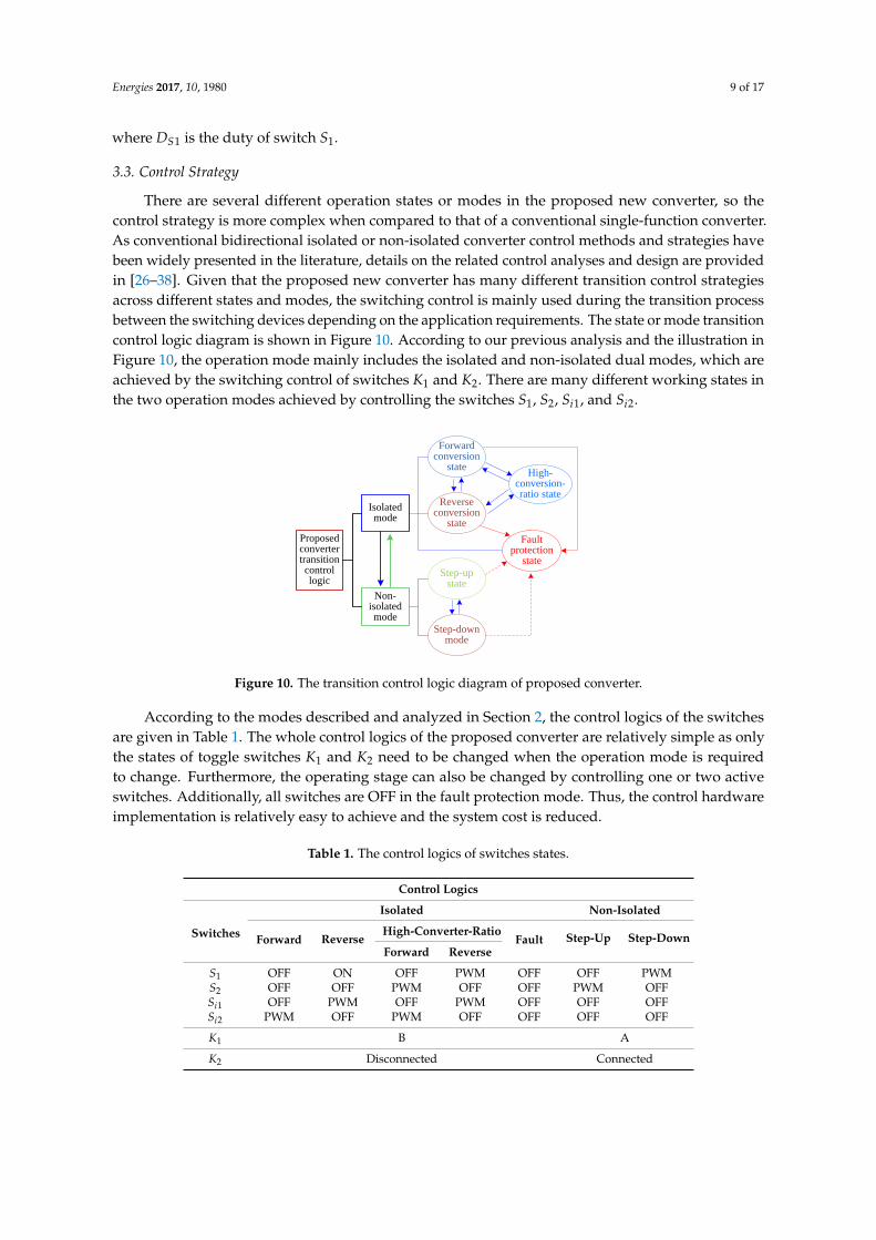
Figure 10. The transition control logic diagram of proposed converter.
According to the modes described and analyzed in Section 2, the control logics of the switches
are given in Table 1. The whole control logics of the proposed converter are relatively simple as only
the states of toggle switches K1 and K2 need to be changed when the operation mode is required to
change. Furthermore, the operating stage can also be changed by controlling one or two active
switches. Additionally, all switches are OFF in the fault protection mode. Thus, the control hardware
implementation is relatively easy to achieve and the system cost is reduced.
Table 1. The control logics of switches states.
Control Logics
Switches
Isolated Non-Isolated
Forward Reverse High-Converter-Ratio
Fault Step-Up Step-Down Forward Reverse
S1 OFF ON OFF PWM OFF OFF PWM
S2 OFF OFF PWM OFF OFF PWM OFF
Si1 OFF PWM OFF PWM OFF OFF OFF
Si2 PWM OFF PWM OFF OFF OFF OFF
K1 B A
K2 Disconnected Connected
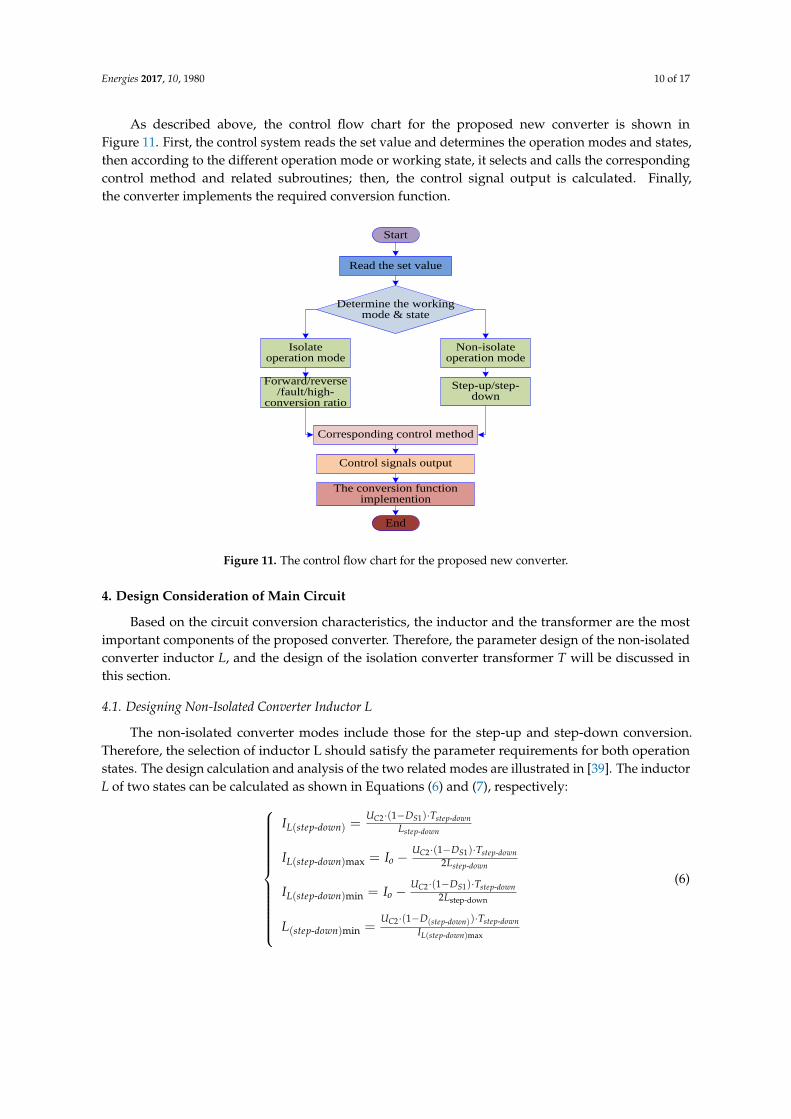
As described above, the control flow chart for the proposed new converter is shown in Figure 11.
First, the control system reads the set value and determines the operation modes and states, then
according to the different operation mode or working state, it selects and calls the corresponding
control method and related subroutines; then, the control signal output is calculated. Finally, the
converter implements the required conversion function.
Figure 10. The transition control logic diagram of proposed converter.
According to the modes described and analyzed in Section 2, the control logics of the switchesare given in Table 1. The whole control logics of the proposed converter are relatively simple as onlythe states of toggle switches K1 and K2 need to be changed when the operation mode is requiredto change. Furthermore, the operating stage can also be changed by controlling one or two activeswitches. Additionally, all switches are OFF in the fault protection mode. Thus, the control hardwareimplementation is relatively easy to achieve and the system cost is reduced.
Table 1. The control logics of switches states.
Control Logics
Switches
Isolated Non-Isolated
Forward ReverseHigh-Converter-Ratio
Fault Step-Up Step-DownForward Reverse
S1 OFF ON OFF PWM OFF OFF PWMS2 OFF OFF PWM OFF OFF PWM OFFSi1 OFF PWM OFF PWM OFF OFF OFFSi2 PWM OFF PWM OFF OFF OFF OFF
K1 B A
K2 Disconnected Connected
Energies 2017, 10, 1980 10 of 17
As described above, the control flow chart for the proposed new converter is shown inFigure 11. First, the control system reads the set value and determines the operation modes and states,then according to the different operation mode or working state, it selects and calls the correspondingcontrol method and related subroutines; then, the control signal output is calculated. Finally,the converter implements the required conversion function.Energies 2017, 10, 1980 10 of 17
Start
Read the set value
Determine the working mode & state
Isolate operation mode
Non-isolate operation mode
Forward/reverse/fault/high-
conversion ratio
Step-up/step-down
Corresponding control method
Control signals output
The conversion function implemention
End
Figure 11. The control flow chart for the proposed new converter.
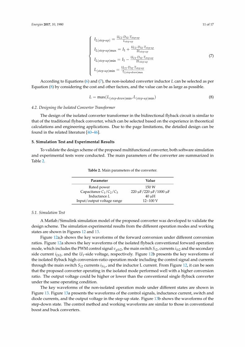
4. Design Consideration of Main Circuit
Based on the circuit conversion characteristics, the inductor and the transformer are the most
important components of the proposed converter. Therefore, the parameter design of the non-
isolated converter inductor L, and the design of the isolation converter transformer T will be
discussed in this section.
4.1. Designing Non-Isolated Converter Inductor L
The non-isolated converter modes include those for the step-up and step-down conversion.
Therefore, the selection of inductor L should satisfy the parameter requirements for both operation
states. The design calculation and analysis of the two related modes are illustrated in [39]. The
inductor L of two states can be calculated as shown in Equations (6) and (7), respectively:
2 1
-
-
2 1
- max
-
2 1
- min
step-down
2 -
- min
1-=
1-
2
1-
2L
1-
step down
step down
step down
step down
C S
L step down
step down
C S
L step down o
step down
C S
L step down o
C step down
step down
U D TI
L
U D TI I
L
U D TI I
U D TL
I
( )
( )
( )
( )
( )
( )
( )
( )
( )
- maxL step down
( )
(6)
Figure 11. The control flow chart for the proposed new converter.
4. Design Consideration of Main Circuit
Based on the circuit conversion characteristics, the inductor and the transformer are the mostimportant components of the proposed converter. Therefore, the parameter design of the non-isolatedconverter inductor L, and the design of the isolation converter transformer T will be discussed inthis section.
4.1. Designing Non-Isolated Converter Inductor L
The non-isolated converter modes include those for the step-up and step-down conversion.Therefore, the selection of inductor L should satisfy the parameter requirements for both operationstates. The design calculation and analysis of the two related modes are illustrated in [39]. The inductorL of two states can be calculated as shown in Equations (6) and (7), respectively:
IL(step-down) =UC2·(1−DS1)·Tstep-down
Lstep-down
IL(step-down)max = Io −UC2·(1−DS1)·Tstep-down
2Lstep-down
IL(step-down)min = Io −UC2·(1−DS1)·Tstep-down
2Lstep-down
L(step-down)min =UC2·(1−D(step-down))·Tstep-down
IL(step-down)max
(6)
Energies 2017, 10, 1980 11 of 17
IL(step-up) =UC2·DS2·Tstep-up
Lstep-up
IL(step-up)max = I1 +UC2·DS2·Tstep-up
2Lstep-up
IL(step-up)min = I1 −UC2·DS2·Tstep-up
2Lstep-up
L(step-up)min =UC2·DS2·Tstep-upIL(step-down)max
(7)
According to Equations (6) and (7), the non-isolated converter inductor L can be selected as perEquation (8) by considering the cost and other factors, and the value can be as large as possible.
L = max(L(step-down)min, L(step-up)min) (8)
4.2. Designing the Isolated Converter Transformer
The design of the isolated converter transformer in the bidirectional flyback circuit is similar tothat of the traditional flyback converter, which can be selected based on the experience in theoreticalcalculations and engineering applications. Due to the page limitations, the detailed design can befound in the related literature [40–46].
5. Simulation Test and Experimental Results
To validate the design scheme of the proposed multifunctional converter, both software simulationand experimental tests were conducted. The main parameters of the converter are summarized inTable 2.
Table 2. Main parameters of the converter.
Parameter Value
Rated power 150 WCapacitance C1/C2/C3 220 µF/220 µF/1000 µF
Inductance L 40 µHInput/output voltage range 12~100 V
5.1. Simulation Test
A Matlab/Simulink simulation model of the proposed converter was developed to validate thedesign scheme. The simulation experimental results from the different operation modes and workingstates are shown in Figures 12 and 13.
Figure 12a,b shows the key waveforms of the forward conversion under different conversionratios. Figure 12a shows the key waveforms of the isolated flyback conventional forward operationmode, which includes the PWM control signal νgSi2, the main switch Si2, currents iSi2 and the secondaryside current iDi2, and the U1-side voltage, respectively. Figure 12b presents the key waveforms ofthe isolated flyback high conversion-ratio operation mode including the control signal and currentsthrough the main switch Si2 currents iSi2 , and the inductor L current. From Figure 12, it can be seenthat the proposed converter operating in the isolated mode performed well with a higher conversionratio. The output voltage could be higher or lower than the conventional single flyback converterunder the same operating condition.
The key waveforms of the non-isolated operation mode under different states are shown inFigure 13. Figure 13a presents the waveforms of the control signals, inductance current, switch anddiode currents, and the output voltage in the step-up state. Figure 13b shows the waveforms of thestep-down state. The control method and working waveforms are similar to those in conventionalboost and buck converters.
Energies 2017, 10, 1980 12 of 17
Energies 2017, 10, 1980 12 of 17
(a) (b)
Figure 12. Simulation results for the converter under isolated mode: (a) the forward converter under
isolated mode; and (b) the isolated high conversion-ratio operation mode.
(a) (b)
Figure 13. Simulation results for the converter under non-isolated mode: (a) the forward converter
under non-isolated mode; and (b) the reserve converter under non-isolated mode.
Figure 12a,b shows the key waveforms of the forward conversion under different conversion
ratios. Figure 12a shows the key waveforms of the isolated flyback conventional forward operation
mode, which includes the PWM control signal νgSi2, the main switch Si2, currents iSi2 and the secondary
side current iDi2, and the U1-side voltage, respectively. Figure 12b presents the key waveforms of the
isolated flyback high conversion-ratio operation mode including the control signal and currents
through the main switch Si2 currents iSi2, and the inductor L current. From Figure 12, it can be seen
that the proposed converter operating in the isolated mode performed well with a higher conversion
ratio. The output voltage could be higher or lower than the conventional single flyback converter
under the same operating condition.
The key waveforms of the non-isolated operation mode under different states are shown in
Figure 13. Figure 13a presents the waveforms of the control signals, inductance current, switch and
diode currents, and the output voltage in the step-up state. Figure 13b shows the waveforms of the
step-down state. The control method and working waveforms are similar to those in conventional
boost and buck converters.
Figure 12. Simulation results for the converter under isolated mode: (a) the forward converter underisolated mode; and (b) the isolated high conversion-ratio operation mode.
Energies 2017, 10, 1980 12 of 17
(a) (b)
Figure 12. Simulation results for the converter under isolated mode: (a) the forward converter under
isolated mode; and (b) the isolated high conversion-ratio operation mode.
(a) (b)
Figure 13. Simulation results for the converter under non-isolated mode: (a) the forward converter
under non-isolated mode; and (b) the reserve converter under non-isolated mode.
Figure 12a,b shows the key waveforms of the forward conversion under different conversion
ratios. Figure 12a shows the key waveforms of the isolated flyback conventional forward operation
mode, which includes the PWM control signal νgSi2, the main switch Si2, currents iSi2 and the secondary
side current iDi2, and the U1-side voltage, respectively. Figure 12b presents the key waveforms of the
isolated flyback high conversion-ratio operation mode including the control signal and currents
through the main switch Si2 currents iSi2, and the inductor L current. From Figure 12, it can be seen
that the proposed converter operating in the isolated mode performed well with a higher conversion
ratio. The output voltage could be higher or lower than the conventional single flyback converter
under the same operating condition.
The key waveforms of the non-isolated operation mode under different states are shown in
Figure 13. Figure 13a presents the waveforms of the control signals, inductance current, switch and
diode currents, and the output voltage in the step-up state. Figure 13b shows the waveforms of the
step-down state. The control method and working waveforms are similar to those in conventional
boost and buck converters.
Figure 13. Simulation results for the converter under non-isolated mode: (a) the forward converterunder non-isolated mode; and (b) the reserve converter under non-isolated mode.
5.2. Experimental Results
The performance and effectiveness of the proposed converter were verified in an experimentalprototype. Experimental tests were conducted with a simulated photovoltaic storage applicationsystem under different operation modes and working conditions. Figure 14 shows the measuredwaveforms of the proposed converter in the isolated mode.
Energies 2017, 10, 1980 13 of 17
Energies 2017, 10, 1980 13 of 17
5.2. Experimental Results
The performance and effectiveness of the proposed converter were verified in an
experimental prototype. Experimental tests were conducted with a simulated photovoltaic
storage application system under different operation modes and working conditions. Figure 14
shows the measured waveforms of the proposed converter in the isolated mode.
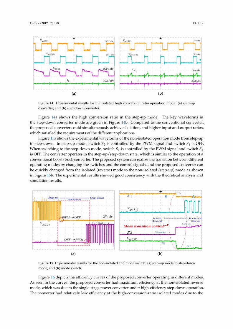
(a) (b)
Figure 14. Experimental results for the isolated high conversion ratio operation mode: (a) step-up
converter; and (b) step-down converter.
Figure 14a shows the high conversion ratio in the step-up mode. The key waveforms in the
step-down converter mode are given in Figure 14b. Compared to the conventional converter, the
proposed converter could simultaneously achieve isolation, and higher input and output ratios,
which satisfied the requirements of the different applications.
Figure 15a shows the experimental waveforms of the non-isolated operation mode from step-up
to step-down. In step-up mode, switch S2 is controlled by the PWM signal and switch S1 is OFF. When
switching to the step-down mode, switch S1 is controlled by the PWM signal and switch S2 is OFF.
The converter operates in the step-up/step-down state, which is similar to the operation of a
conventional boost/buck converter. The proposed system can realize the transition between different
operating modes by changing the switches and the control signals, and the proposed converter can
be quickly changed from the isolated (reverse) mode to the non-isolated (step-up) mode as shown in
Figure 15b. The experimental results showed good consistency with the theoretical analysis and
simulation results.
(a) (b)
Figure 15. Experimental results for the non-isolated and mode switch: (a) step-up mode to step-down
mode; and (b) mode switch.
Figure 14. Experimental results for the isolated high conversion ratio operation mode: (a) step-upconverter; and (b) step-down converter.
Figure 14a shows the high conversion ratio in the step-up mode. The key waveforms inthe step-down converter mode are given in Figure 14b. Compared to the conventional converter,the proposed converter could simultaneously achieve isolation, and higher input and output ratios,which satisfied the requirements of the different applications.
Figure 15a shows the experimental waveforms of the non-isolated operation mode from step-upto step-down. In step-up mode, switch S2 is controlled by the PWM signal and switch S1 is OFF.When switching to the step-down mode, switch S1 is controlled by the PWM signal and switch S2
is OFF. The converter operates in the step-up/step-down state, which is similar to the operation of aconventional boost/buck converter. The proposed system can realize the transition between differentoperating modes by changing the switches and the control signals, and the proposed converter canbe quickly changed from the isolated (reverse) mode to the non-isolated (step-up) mode as shownin Figure 15b. The experimental results showed good consistency with the theoretical analysis andsimulation results.
Energies 2017, 10, 1980 13 of 17
5.2. Experimental Results
The performance and effectiveness of the proposed converter were verified in an
experimental prototype. Experimental tests were conducted with a simulated photovoltaic
storage application system under different operation modes and working conditions. Figure 14
shows the measured waveforms of the proposed converter in the isolated mode.
(a) (b)
Figure 14. Experimental results for the isolated high conversion ratio operation mode: (a) step-up
converter; and (b) step-down converter.
Figure 14a shows the high conversion ratio in the step-up mode. The key waveforms in the
step-down converter mode are given in Figure 14b. Compared to the conventional converter, the
proposed converter could simultaneously achieve isolation, and higher input and output ratios,
which satisfied the requirements of the different applications.
Figure 15a shows the experimental waveforms of the non-isolated operation mode from step-up
to step-down. In step-up mode, switch S2 is controlled by the PWM signal and switch S1 is OFF. When
switching to the step-down mode, switch S1 is controlled by the PWM signal and switch S2 is OFF.
The converter operates in the step-up/step-down state, which is similar to the operation of a
conventional boost/buck converter. The proposed system can realize the transition between different
operating modes by changing the switches and the control signals, and the proposed converter can
be quickly changed from the isolated (reverse) mode to the non-isolated (step-up) mode as shown in
Figure 15b. The experimental results showed good consistency with the theoretical analysis and
simulation results.
(a) (b)
Figure 15. Experimental results for the non-isolated and mode switch: (a) step-up mode to step-down
mode; and (b) mode switch. Figure 15. Experimental results for the non-isolated and mode switch: (a) step-up mode to step-downmode; and (b) mode switch.
Figure 16 depicts the efficiency curves of the proposed converter operating in different modes.As seen in the curves, the proposed converter had maximum efficiency at the non-isolated reversemode, which was due to the single-stage power converter under high-efficiency step-down operation.The converter had relatively low efficiency at the high-conversion-ratio isolated modes due to the
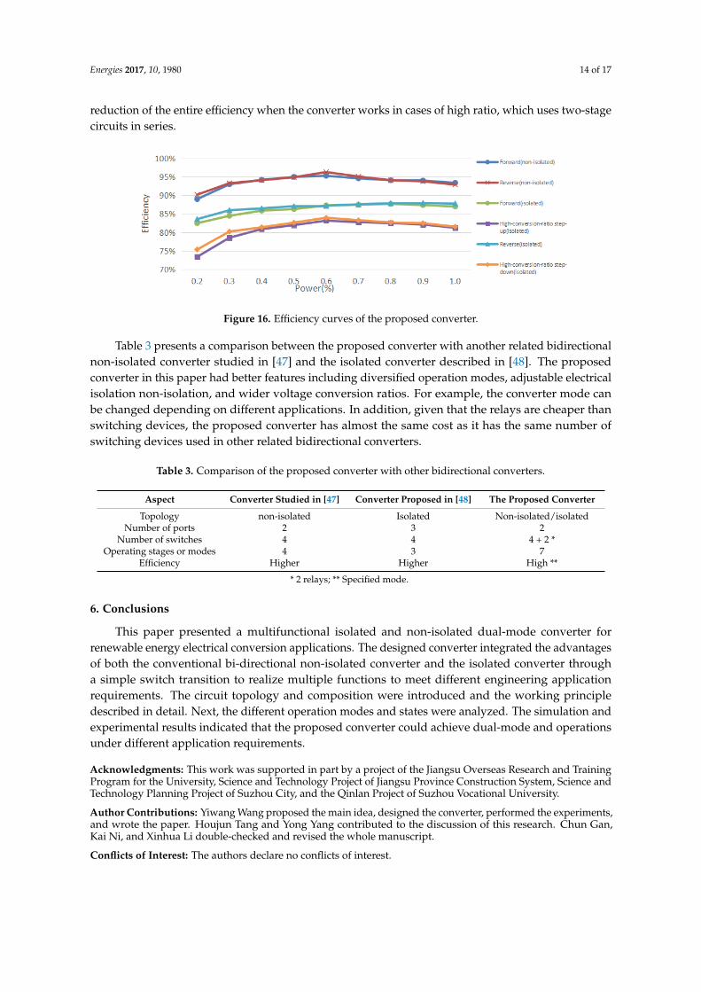
Energies 2017, 10, 1980 14 of 17
reduction of the entire efficiency when the converter works in cases of high ratio, which uses two-stagecircuits in series.
Energies 2017, 10, 1980 14 of 17
Figure 16 depicts the efficiency curves of the proposed converter operating in different modes.
As seen in the curves, the proposed converter had maximum efficiency at the non-isolated reverse
mode, which was due to the single-stage power converter under high-efficiency step-down operation.
The converter had relatively low efficiency at the high-conversion-ratio isolated modes due to the
reduction of the entire efficiency when the converter works in cases of high ratio, which uses two-
stage circuits in series.
Figure 16. Efficiency curves of the proposed converter.
Table 3 presents a comparison between the proposed converter with another related
bidirectional non-isolated converter studied in [47] and the isolated converter described in [48]. The
proposed converter in this paper had better features including diversified operation modes,
adjustable electrical isolation non-isolation, and wider voltage conversion ratios. For example, the
converter mode can be changed depending on different applications. In addition, given that the
relays are cheaper than switching devices, the proposed converter has almost the same cost as it has
the same number of switching devices used in other related bidirectional converters.
Table 3. Comparison of the proposed converter with other bidirectional converters.
Aspect Converter Studied in [47] Converter Proposed in [48] The Proposed Converter
Topology non-isolated Isolated Non-isolated/isolated
Number of ports 2 3 2
Number of switches 4 4 4 + 2 *
Operating stages or modes 4 3 7
Efficiency Higher Higher High **
* 2 relays; ** Specified mode.
6. Conclusions
This paper presented a multifunctional isolated and non-isolated dual-mode converter for
renewable energy electrical conversion applications. The designed converter integrated the
advantages of both the conventional bi-directional non-isolated converter and the isolated converter
through a simple switch transition to realize multiple functions to meet different engineering
application requirements. The circuit topology and composition were introduced and the working
principle described in detail. Next, the different operation modes and states were analyzed. The
simulation and experimental results indicated that the proposed converter could achieve dual-mode
and operations under different application requirements.
Acknowledgments: This work was supported in part by a project of the Jiangsu Overseas Research and Training
Program for the University, Science and Technology Project of Jiangsu Province Construction System, Science
and Technology Planning Project of Suzhou City, and the Qinlan Project of Suzhou Vocational University.
Author Contributions: Yiwang Wang proposed the main idea, designed the converter, performed the
experiments, and wrote the paper. Houjun Tang and Yong Yang contributed to the discussion of this research.
Chun Gan, Kai Ni, and Xinhua Li double-checked and revised the whole manuscript.
Conflicts of Interest: The authors declare no conflicts of interest.
Figure 16. Efficiency curves of the proposed converter.
Table 3 presents a comparison between the proposed converter with another related bidirectionalnon-isolated converter studied in [47] and the isolated converter described in [48]. The proposedconverter in this paper had better features including diversified operation modes, adjustable electricalisolation non-isolation, and wider voltage conversion ratios. For example, the converter mode canbe changed depending on different applications. In addition, given that the relays are cheaper thanswitching devices, the proposed converter has almost the same cost as it has the same number ofswitching devices used in other related bidirectional converters.
Table 3. Comparison of the proposed converter with other bidirectional converters.
Aspect Converter Studied in [47] Converter Proposed in [48] The Proposed Converter
Topology non-isolated Isolated Non-isolated/isolatedNumber of ports 2 3 2
Number of switches 4 4 4 + 2 *Operating stages or modes 4 3 7
Efficiency Higher Higher High **
* 2 relays; ** Specified mode.
6. Conclusions
This paper presented a multifunctional isolated and non-isolated dual-mode converter forrenewable energy electrical conversion applications. The designed converter integrated the advantagesof both the conventional bi-directional non-isolated converter and the isolated converter througha simple switch transition to realize multiple functions to meet different engineering applicationrequirements. The circuit topology and composition were introduced and the working principledescribed in detail. Next, the different operation modes and states were analyzed. The simulation andexperimental results indicated that the proposed converter could achieve dual-mode and operationsunder different application requirements.
Acknowledgments: This work was supported in part by a project of the Jiangsu Overseas Research and TrainingProgram for the University, Science and Technology Project of Jiangsu Province Construction System, Science andTechnology Planning Project of Suzhou City, and the Qinlan Project of Suzhou Vocational University.
Author Contributions: Yiwang Wang proposed the main idea, designed the converter, performed the experiments,and wrote the paper. Houjun Tang and Yong Yang contributed to the discussion of this research. Chun Gan,Kai Ni, and Xinhua Li double-checked and revised the whole manuscript.
Conflicts of Interest: The authors declare no conflicts of interest.
Energies 2017, 10, 1980 15 of 17
References
1. Tseng, K.; Huang, C.; Cheng, C. A Single-Switch Converter with High Step-Up Gain and Low Diode VoltageStress Suitable for Green Power-Source Conversion. IEEE J. Emerg. Sel. Top. Power Electron. 2016, 4, 363–372.[CrossRef]
2. Xu, W.; Li, Y.; Gong, X.; Hong, Z.; Killat, D. A Dual-Mode Single-Inductor Dual-Output Switching Converterwith Small Ripple. IEEE Trans. Power Electron. 2010, 25, 614–623.
3. Singh, B.; Shrivastava, A. Buck converter-based power supply design for low power light emitting diodelamp lighting. IET Power Electron. 2014, 7, 946–956. [CrossRef]
4. EI Khateb, A.H.; Rahim, N.A.; Selvaraj, J.; Williams, B.W. DC-to-DC Converter with Low Input CurrentRipple for Maximum Photovoltaic Power Extraction. IEEE Trans. Ind. Electron. 2015, 62, 2246–2256.[CrossRef]
5. Zeng, J.; Qiao, W.; Qu, L. An Isolated Three-Port Bidirectional DC-DC Converter for Photovoltaic Systemswith Energy Storage. IEEE Trans. Ind. Appl. 2015, 51, 3493–3503. [CrossRef]
6. Kouro, S.; Leon, J.I.; Vinnikov, D.; Franquelo, L.G. Grid-Connected Photovoltaic Systems: An Overview ofRecent Research and Emerging PV Converter Technology. IEEE Ind. Electron. Mag. 2015, 9, 47–61. [CrossRef]
7. Shen, C.; Shen, Y.; Tsai, C. Isolated DC-DC Converter for Bidirectional Power Flow Controlling withSoft-Switching Feature and High Step-Up/Down Voltage Conversion. Energies 2017, 10, 296. [CrossRef]
8. Tseng, S.; Wang, H. A Photovoltaic Power System Using a High Step-up Converter for DC Load Applications.Energies 2013, 6, 1068–1100. [CrossRef]
9. Xue, Y.; Chang, L.; Kjaer, S.B.; Bordonau, J.; Shimizu, T. Topologies of single-phase inverters for smalldistributed power generators: An overview. IEEE Trans. Power Electron. 2004, 19, 1305–1314. [CrossRef]
10. Chomsuwan, K.; Prisuwanna, P.; Monyakul, V. Photovoltaic grid-connected inverter using two-switchbuck-boost converter. In Proceedings of the Photovoltaic Specialists Conference, New Orleans, LA, USA,19–24 May 2002.
11. Gonzalez, R.; Lopez, J.; Sanchis, P.; Marroyo, L. Transformerless Inverter for Single-Phase PhotovoltaicSystems. IEEE Trans. Power Electron. 2007, 22, 693–697. [CrossRef]
12. Kerekes, T.; Teodorescu, R.; Rodriguez, P.; Vazquez, G.; Aldabas, E. A New High-Efficiency Single-PhaseTransformerless PV Inverter Topology. IEEE Trans. Ind. Electron. 2011, 58, 184–191. [CrossRef]
13. Daher, S.; Schmid, J.; Antunes, F.L.M. Multilevel Inverter Topologies for Stand-Alone PV Systems. IEEE Trans.Ind. Electron. 2008, 55, 2703–2712. [CrossRef]
14. Sher, H.A.; Rizvi, A.A.; Addoweesh, K.E.; Al-Haddad, K. A Single Stage Stand-Alone Photovoltaic EnergySystem (SAPES) with High Tracking Efficiency. IEEE Trans. Sustain. Energy 2016, 8, 755–762. [CrossRef]
15. Wai, R.; Wang, W.; Lin, C. High-Performance Stand-Alone Photovoltaic Generation System. IEEE Trans.Ind. Electron. 2008, 55, 240–250. [CrossRef]
16. Wang, W.; Ruan, X. A Modified Reference of an Intermediate Bus Capacitor Voltage-Based Second-HarmonicCurrent Reduction Method for a Standalone Photovoltaic Power System. IEEE Trans. Power Electron. 2016,31, 5562–5573. [CrossRef]
17. Jabir, H.; Mekhilef, S.; Nakaoka, M.; Nishida, K. Development of a transformer-based multilevel invertertopology for stand-alone photovoltaic system. In Proceedings of the Power Electronics and Applications(EPE 2013), Lille, France, 2–6 September 2013.
18. Parsekar, S.; Chatterjee, K. A Novel Strategy for Battery Placement in Standalone Solar Photovoltaic ConverterSystem. In Proceedings of the 2014 IEEE 40th Photovoltaic Specialist Conference (PVSC), Denver, CO, USA,8–13 June 2014; pp. 2751–2756.
19. Geibel, D.; Jahn, J.; Juchem, R. Simulation model based control development of a multifunctionalPV-inverter. In Proceedings of the 2007 European Conference on Power Electronics and Applications (EPE),Aalborg, Denmark, 2–5 September 2007.
20. Wong, Y.; Chen, J.; Liu, K.; Hsieh, Y. A Novel High Step-Up DC-DC Converter with Coupled Inductor andSwitched Clamp Capacitor Techniques for Photovoltaic Systems. Energies 2017, 10, 378. [CrossRef]
21. Shen, C.; Chen, H.; Chiu, P. Integrated Three-Voltage-Booster DC-DC Converter to Achieve High VoltageGain with Leakage-Energy Recycling for PV or Fuel-Cell Power Systems. Energies 2015, 8, 9843–9859.[CrossRef]
Energies 2017, 10, 1980 16 of 17
22. Li, X.; Zhang, H.; Balog, R. Control Strategy for Seamless Transfer between Island and Grid-ConnectedOperation for a Dual Mode Photovoltaic Inverter. In Proceedings of the Energy Conversion Congress andExposition (ECCE 2015), Montreal, QC, Canada, 20–24 September 2015.
23. Zeng, Z.; Yang, H.; Tang, S.; Zhao, R. Objective-Oriented Power Quality Compensation of MultifunctionalGrid-Tied Inverters and Its Application in Microgrids. IEEE Trans. Power Electron. 2015, 30, 1255–1265.[CrossRef]
24. Ye, T.; Dai, N.; Lam, C.; Wong, M.; Guerrero, J.M. Analysis, Design, and Implementation of aQuasi-Proportional-Resonant Controller for a Multifunctional Capacitive-Coupling Grid-Connected Inverter.IEEE Trans. Ind. Appl. 2016, 52, 4269–4280. [CrossRef]
25. Shin, J.; Choi, S.; Cho, B. High-Efficiency Bridgeless Flyback Rectifier with Bidirectional Switch and DualOutput Windings. IEEE Trans. Power Electron. 2014, 29, 4752–4762. [CrossRef]
26. De Melo, M.F.; Vizzotto, W.D.; Quintana, P.J.; Kirsten, A.L.; Costa, M.A.D.; Garcia, J. Bidirectional Grid-TieFlyback Converter Applied to Distributed Power Generation and Street Lighting Integrated System.IEEE Trans. Ind. Appl. 2015, 51, 4709–4718. [CrossRef]
27. Thummala, P.; Zhang, Z.; Andersen, M.A. High Voltage Bi-directional Flyback Converter for CapacitiveActuator. In Proceedings of the 2013 15th European Conference on Power Electronics and Applications(EPE), Lille, France, 2–6 September 2013.
28. Huang, X.; Lee, F.C.; Li, Q.; Du, W. High-Frequency High-Efficiency GaN-Based Interleaved CRMBidirectional Buck/Boost Converter with Inverse Coupled Inductor. IEEE Trans. Power Electron. 2016,31, 4343–4352. [CrossRef]
29. Viinamäki, J.; Kuperman, A.; Suntio, T. Grid-Forming-Mode Operation of Boost-Power-Stage Converter inPV-Generator-Interfacing Applications. Energies 2017, 10, 1033.
30. Zhao, F.; Zhang, X.; Wen, X.; Zhao, L.; Guo, Q.; Zhang, G. A Novel Control Scheme for Bi-directional BuckBoost Converter. In Proceedings of the 2013 International Conference on Electrical Machines and Systems,Busan, Korea, 26–29 October 2013.
31. Zhang, C.; Jiang, D.; Zheng, H.; Ye, L. A Bi-directional Buck/Boost Voltage Balancer for DC DistributionSystem. In Proceedings of the Fourth International Conference on Digital Manufacturing & Automation,Qindao, China, 29–30 June 2013.
32. Ardi, H.; Ahrabi, R.R.; Ravadanegh, S.N. Non-isolated bidirectional DC-DC converter analysis andimplementation. IET Power Electron. 2014, 7, 3033–3044. [CrossRef]
33. Zheng, X.; Ali, H.; Wu, X.; Zaman, H.; Khan, S. Non-Linear Behavioral Modeling for DC-DC Converters andDynamic Analysis of Distributed Energy Systems. Energies 2017, 10, 63. [CrossRef]
34. Hamasaki, S.; Yano, Y.; Fukuda, H.; Tsuji, M. Deadbeat Control of Bidirectional Buck/boost DC-DC Converterfor Power Leveling System with EDLC. In Proceedings of the 2015 41st IEEE Annual Conference of theIndustrial Electronics Society, Yokohama, Japan, 9–12 November 2015.
35. McCurlie, L.; Preindl, M.; Malysz, P.; Emad, A. Simplified Control for Redistributive Balancing Systems usingBidirectional Flyback Converters. In Proceedings of the 2015 IEEE Transportation Electrification Conferenceand Expo (ITEC2015), Dearborn, MI, USA, 14–17 June 2015.
36. Hoffstadt, T.; Maas, J. Sensorless BCM control for a bidirectional flyback-converter. In Proceedings ofthe 42nd Annual Conference of the IEEE Industrial Electronics Society, IECON 2016, Florence, Italy,24–27 October 2016.
37. Thummala, P.; Maksimovic, D.; Zhang, Z.; Andersen, M.A.E. Digital Control of a High-Voltage (2.5 kV)Bidirectional DC-DC Flyback Converter for Driving a Capacitive Incremental Actuator. IEEE Trans.Power Electron. 2016, 31, 8500–8516. [CrossRef]
38. Saranya, P.S.; Chandran, L.R. Analysis of bidirectional flyback converter. In Proceedings of the 2015International Conference on Computation of Power, Energy, Information and Communication (ICCPEIC),Chennai, India, 22–23 April 2015.
39. Pressman, A.I.; Billings, K.H.; Morey, T. Switching Power Supply Design, 3rd ed.; McGraw-Hill: New York, NY,USA, 2009.
40. Trzynadlowski, A.M. Power Electronic Converters and Systems: Frontiers and Applications; The Institution ofEngineering and Technology: London, UK, 1 February 2016.
41. Patin, N. Power Electronics Applied to Industrial Systems and Transports; ISTE Press and Elsevier: London, UK,May 2015; Chapter 2; pp. 19–39.
Energies 2017, 10, 1980 17 of 17
42. Padiyar, U.S.; Kamath, V. Design and Implementation of a Universal Input Flyback Converter. In Proceedingsof the International Conference on Electrical, Electronics, and Optimization Techniques (ICEEOT), Chennai,India, 3–5 March 2016; pp. 3428–3433.
43. Lee, I.; Lee, J. A High-Power DC-DC Converter Topology for Battery Charging Applications. Energies 2017,10, 871. [CrossRef]
44. Hu, J.; Cheng, K.W.E. Predictive control of power electronics converters in renewable energy systems.Energies 2017, 10, 515. [CrossRef]
45. Chung, H.S.H.; Cheung, W.; Tang, K. A ZCS Bidirectional Flyback Converter. In Proceedings of the 2004 35thAnnual IEEE Power Electronics Specialists Conference, Aachen, Germany, 20–25 June 2004; pp. 1506–1512.
46. Wu, H.; Sun, K.; Chen, L.; Zhu, L.; Xing, Y. High Step-Up/Step-Down Soft-Switching Bidirectional DC–DCConverter with Coupled-Inductor and Voltage Matching Control for Energy Storage Systems. IEEE Trans.Ind. Electron. 2016, 63, 2892–2903. [CrossRef]
47. Liu, K.; Liu, C.; Liu, Y.; Chien, Y.; Wang, B. Analysis and Controller Design of a Universal BidirectionalDC-DC Converter. Energies 2016, 9, 501. [CrossRef]
48. Wu, Y.; Chiu, P. A High-Efficiency Isolated-Type Three-Port Bidirectional DC/DC Converter for PhotovoltaicSystems. Energies 2017, 10, 434. [CrossRef]
© 2017 by the authors. Licensee MDPI, Basel, Switzerland. This article is an open accessarticle distributed under the terms and conditions of the Creative Commons Attribution(CC BY) license (http://creativecommons.org/licenses/by/4.0/).