MLX73290-M - Melexis · Compliant to EN 300 220, DASH7, FCC part 15, ARIB STD-T67, IEEE802.15.4 and...
53
MLX73290-M 300 to 960MHz Multi-Channel Transceiver With Flex RF Front-End REVISION 010 – DECEMBER 22, 2016 3901073290 1. Features and Benefits Flex TX/RX RF front-end for antenna and frequency diversity Energy harvesting interface Transmitter with power detectors Receiver with digital RSSI Receiver self polling with MCU wake-up Multi-band frequency coverage from 300MHz up to 960MHz Modulation schemes supported: (G)FSK, (G)MSK, (G)OOK Transmitter power of -20 to 13dBm, 64 steps Receiver sensitivity of -120dBm (FSK, 433MHz, 15kHz CHBW) Supply voltage range of 2.1 to 3.6V PLL synthesizer with 60Hz resolution Channel filter bandwidth of 9 to 600kHz Data rate of 0.3 to 250kbps (GFSK) Frequency deviation up to 125kHz 32MHz crystal frequency Comprehensive supply monitoring & error handling capabilities SPI programmable in stand-by mode Multi-channel sensing and packet recognition 256byte FIFO (can be split 128/128 for RX/TX) 4 programmable GPIO ports 32L QFN5x5 package Compliant to EN 300 220, DASH7, FCC part 15, ARIB STD-T67, IEEE802.15.4 and other standards 2. Application Examples Automatic meter reading (AMR) Remote controls Home and building automation Alarm and security systems Garage door openers Medical applications Telemetry Industrial appliances Automotive keyless entry Tire pressure monitoring 3. Ordering Code Product Temperature Package Option Packaging Form MLX73290 R (-40°C to 105°C) LQ (32L QFN5x5) BBM-000 RE (reel 5000 pcs.) 4. Introduction The MLX73290-M is a 300 to 930MHz multi-channel transceiver chip. The IC is designed for general purpose applications for example in the European bands at 433MHz and 868MHz or for similar applications in North America or Asia, e.g. at 315MHz or 915MHz. It is also well-suited for narrow-band applications which meet the ARIB standard STD- T67 in the frequency range 426MHz to 470MHz. The output power, frequency channel, modulation type and frequency deviation are programmable via the serial programming interface (SPI). The synthesizer operates with a fractional-N PLL and VCO with integrated inductor. The small frequency resolution of the MLX73290-M and its PLL phase noise performance facilitate it for narrow-band operation. There are five selectable modulation schemes: on-off keying (OOK), binary frequency shift keying (FSK) and minimum shift keying (MSK) as well as their Gaussian filtered versions (GFSK and GMSK). The low-IF receiver part comprises fully digital demodulation and self-polling features together with channel scanning and packet recognition.
Transcript of MLX73290-M - Melexis · Compliant to EN 300 220, DASH7, FCC part 15, ARIB STD-T67, IEEE802.15.4 and...

MLX73290-M 300 to 960MHz Multi-Channel Transceiver With Flex RF Front-End
REVISION 010 – DECEMBER 22, 2016
3901073290
1. Features and Benefits
Flex TX/RX RF front-end for antenna and frequency diversity
Energy harvesting interface
Transmitter with power detectors
Receiver with digital RSSI
Receiver self polling with MCU wake-up
Multi-band frequency coverage from 300MHz up to 960MHz
Modulation schemes supported: (G)FSK, (G)MSK, (G)OOK
Transmitter power of -20 to 13dBm, 64 steps
Receiver sensitivity of -120dBm (FSK, 433MHz, 15kHz CHBW)
Supply voltage range of 2.1 to 3.6V
PLL synthesizer with 60Hz resolution
Channel filter bandwidth of 9 to 600kHz
Data rate of 0.3 to 250kbps (GFSK)
Frequency deviation up to 125kHz
32MHz crystal frequency
Comprehensive supply monitoring & error handling capabilities
SPI programmable in stand-by mode
Multi-channel sensing and packet recognition
256byte FIFO (can be split 128/128 for RX/TX)
4 programmable GPIO ports
32L QFN5x5 package
Compliant to EN 300 220, DASH7, FCC part 15, ARIB STD-T67, IEEE802.15.4 and other standards
2. Application Examples
Automatic meter reading (AMR)
Remote controls
Home and building automation
Alarm and security systems
Garage door openers
Medical applications
Telemetry
Industrial appliances
Automotive keyless entry
Tire pressure monitoring
3. Ordering Code
Product Temperature Package Option Packaging Form
MLX73290 R (-40°C to 105°C) LQ (32L QFN5x5) BBM-000 RE (reel 5000 pcs.)
4. Introduction
The MLX73290-M is a 300 to 930MHz multi-channel transceiver chip. The IC is designed for general purpose applications for example in the European bands at 433MHz and 868MHz or for similar applications in North America or Asia, e.g. at 315MHz or 915MHz. It is also well-suited for narrow-band applications which meet the ARIB standard STD-T67 in the frequency range 426MHz to 470MHz.
The output power, frequency channel, modulation type and frequency deviation are programmable via the serial programming interface (SPI). The synthesizer operates with a fractional -N PLL and VCO with integrated inductor. The small frequency resolution of the MLX73290-M and its PLL phase noise performance facilitate it for narrow-band operation. There are five selectable modulation schemes: on-off keying (OOK), binary frequency shift keying (FSK) and minimum shift keying (MSK) as well as their Gaussian filtered versions (GFSK and GMSK). The low-IF receiver part comprises fully digital demodulation and self-polling features together with channel scanning and packet recognition.
MLX73290-M 300 to 960MHz Multi-Channel Transceiver With Flex RF Front-End
Page 2 of 53
REVISION 010 – DECEMBER 22, 2016
3901073290
Contents
1. Features and Benefits ............................................................................................................................ 1
2. Application Examples ............................................................................................................................. 1
3. Ordering Code ....................................................................................................................................... 1
4. Introduction .......................................................................................................................................... 1
5. Version History ...................................................................................................................................... 4
6. Absolute Maximum Ratings ................................................................................................................... 4
7. Pin Definitions and Pin-out .................................................................................................................... 4
8. Electrical Specifications ......................................................................................................................... 6
8.1. Normal Operating Conditions ............................................................................................................ 6
8.2. General Characteristics ...................................................................................................................... 6
8.3. RF Characteristics ................................................................................................................................ 6
8.4. SPI Characteristics ............................................................................................................................... 9
9. Functional Description ........................................................................................................................... 9
9.1. Frequencies and Standards ................................................................................................................ 9
9.2. Block Diagram ................................................................................................................................... 10
9.3. Detailed Description ......................................................................................................................... 10
9.4. RF Transceiver ................................................................................................................................... 11
9.4.1. Flex TX/RX Front-End .................................................................................................................. 11
9.4.2. Frequency Synthesizer ............................................................................................................... 13
9.4.3. Transmit Mode (TX) .................................................................................................................... 13
9.4.4. Receive Mode (RX) ...................................................................................................................... 13
9.4.5. State Machine ............................................................................................................................. 16
9.5. Modulation Settings ......................................................................................................................... 17
9.6. Packet Handler .................................................................................................................................. 18
9.6.1. Preamble ..................................................................................................................................... 19
9.6.2. Sync Word ................................................................................................................................... 19
9.6.3. Packet Length .............................................................................................................................. 19
9.6.4. Address ........................................................................................................................................ 20
9.6.5. CRC16 .......................................................................................................................................... 20
9.6.6. Multi Frame ................................................................................................................................. 20
9.7. Power Management and Energy Harvesting ................................................................................... 21
9.8. Programmable Timer / Clock Generator ......................................................................................... 22
MLX73290-M 300 to 960MHz Multi-Channel Transceiver With Flex RF Front-End
Page 3 of 53
REVISION 010 – DECEMBER 22, 2016
3901073290
9.9. System Timer..................................................................................................................................... 22
9.10. General Purpose ADC ..................................................................................................................... 22
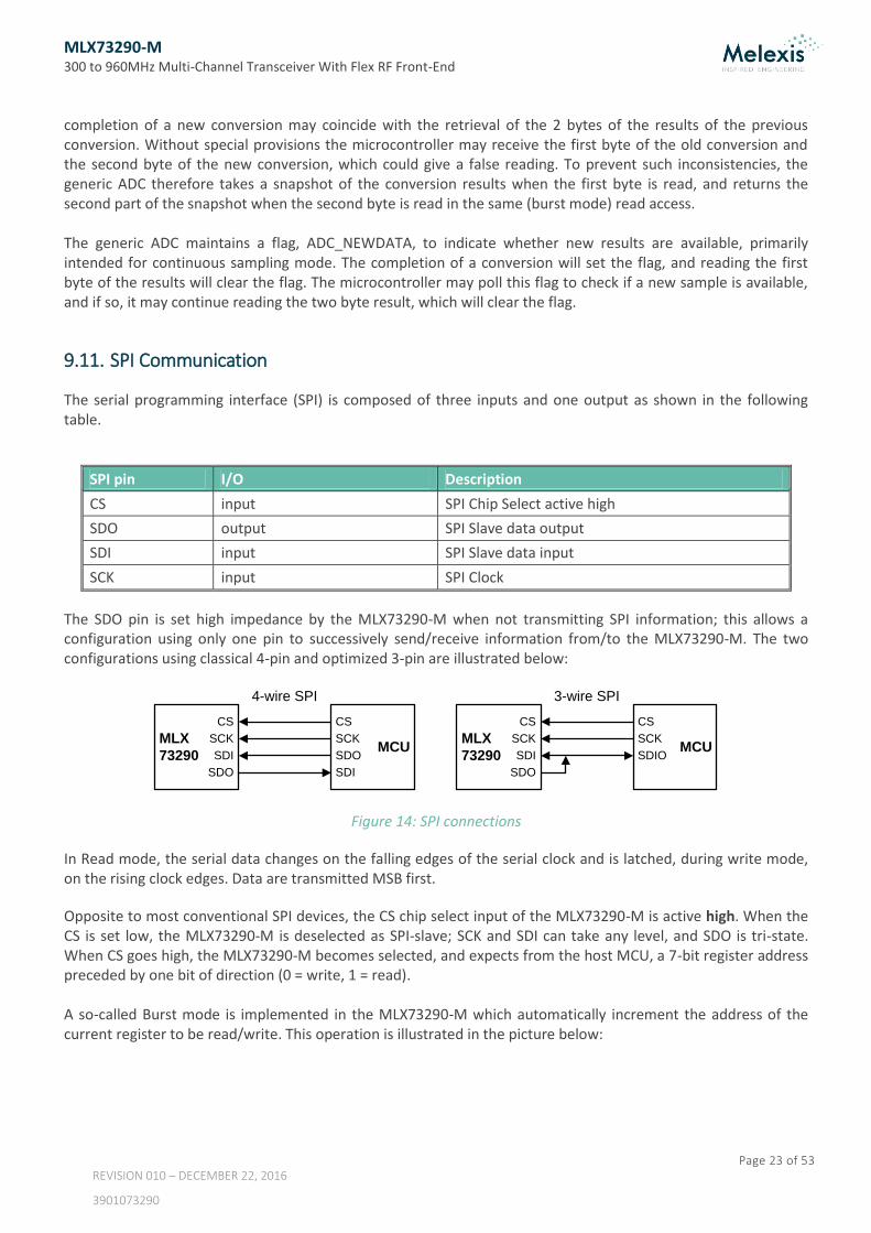
9.11. SPI Communication ......................................................................................................................... 23
9.12. GPIO Pins ......................................................................................................................................... 24
10. Register Settings ................................................................................................................................ 26
10.1. RF Transceiver (0x02 to 0x33) ........................................................................................................ 26
10.2. Status Byte & GPIOs (0x34 to 0x3B) .............................................................................................. 39
10.3. General Purpose ADC (0x3C to 0x3F) ............................................................................................ 40
10.4. Timers (0x40 to 0x4F) ..................................................................................................................... 42
10.5. Chip ID and Soft Reset (register 0x7F) ........................................................................................... 45
10.6. Bank 0 .............................................................................................................................................. 45
11. Application Information ..................................................................................................................... 46
11.1. Typical Application Schematic ........................................................................................................ 46
11.1.1. TX/RX Combining Network ....................................................................................................... 47
11.1.2. Balun .......................................................................................................................................... 47
11.1.3. External Power Switch Usage................................................................................................... 48
12. Performance Plots ............................................................................................................................. 49
12.1. Spectrum Plots ................................................................................................................................ 49
12.2. Eye Diagram .................................................................................................................................... 50
12.3. Phase Noise ..................................................................................................................................... 50
13. Manufacturability of Melexis Products with Different Soldering Processes ....................................... 51
14. ESD Precautions ................................................................................................................................. 51
15. Package Information .......................................................................................................................... 52
16. Contact .............................................................................................................................................. 53
17. Disclaimer .......................................................................................................................................... 53

MLX73290-M 300 to 960MHz Multi-Channel Transceiver With Flex RF Front-End
Page 4 of 53
REVISION 010 – DECEMBER 22, 2016
3901073290
5. Version History
Data sheet version Date Value
Rev 001 July 2012 First public release, preliminary version
Rev 002 Oct 2012 Corrections, packed handler added, preliminary version
Rev 003 Dec 2012 PA control information added
Rev 004 Mar 2013 Receiver self polling with MCU wake-up, register name OOK_MOD changed to RF_BIAS, performance plots added
Rev 005 Jun 2013 ACR, blocking parameters and more performance plots added
Rev 006 Sep 2013 More GPIO description added
Rev 007 Oct 2013 Flow chart for RF state machine added
Rev 008 May 2015 Temperature codes redefined and general update
Rev 009 Sep 2015 General update, modulation settings added
Rev 010 Dec 2016 Carrier frequency acceptance range added
6. Absolute Maximum Ratings
Parameter Symbol Value Units
Supply Voltage VDD 0 to 4 V
Operating Temp. Range TA -40 to 105 C
Storage Temperature Range
TS -55 to 125 C
ESD Sensitivity (HBM) VESD ±2 kV
ESD Sensitivity (CDM) VESD ±0.5 kV
Exceeding the absolute maximum ratings may cause permanent damage. Exposure to absolute -maximum-rated conditions for extended periods may affect device reliability.
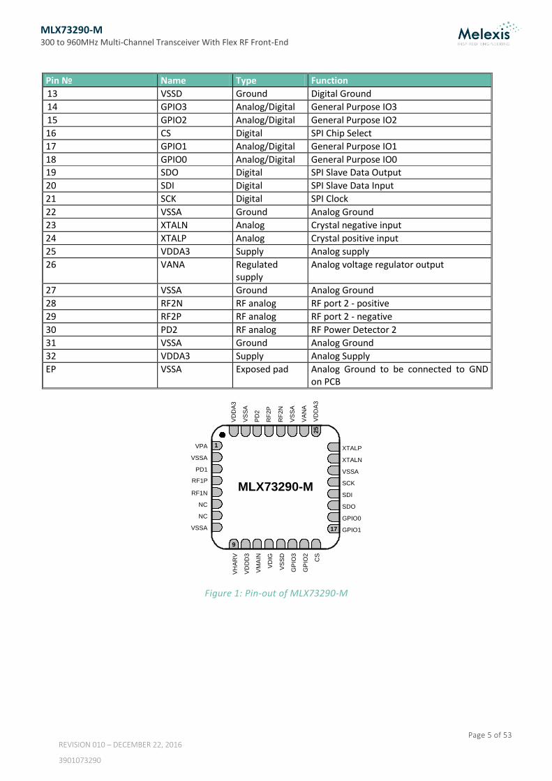
7. Pin Definitions and Pin-out
Pin № Name Type Function
1 VPA Supply Supply of PA
2 VSSA Ground Analog Ground
3 PD1 RF analog RF Power Detector 1
4 RF1P RF analog RF port 1 - positive
5 RF1N RF analog RF port 1 - negative
6 NC Not connected
7 NC Not connected
8 VSSA Ground Analog Ground
9 VHARV Analog Energy harvesting input
10 VDDD3 Supply Battery supply (dedicated to power switch)
11 VMAIN Supply Power switch output for host MCU
12 VDIG Regulated supply
Digital voltage regulator output
MLX73290-M 300 to 960MHz Multi-Channel Transceiver With Flex RF Front-End
Page 5 of 53
REVISION 010 – DECEMBER 22, 2016
3901073290
Pin № Name Type Function
13 VSSD Ground Digital Ground
14 GPIO3 Analog/Digital General Purpose IO3
15 GPIO2 Analog/Digital General Purpose IO2
16 CS Digital SPI Chip Select
17 GPIO1 Analog/Digital General Purpose IO1
18 GPIO0 Analog/Digital General Purpose IO0
19 SDO Digital SPI Slave Data Output
20 SDI Digital SPI Slave Data Input
21 SCK Digital SPI Clock
22 VSSA Ground Analog Ground
23 XTALN Analog Crystal negative input
24 XTALP Analog Crystal positive input
25 VDDA3 Supply Analog supply
26 VANA Regulated supply
Analog voltage regulator output
27 VSSA Ground Analog Ground
28 RF2N RF analog RF port 2 - positive
29 RF2P RF analog RF port 2 - negative
30 PD2 RF analog RF Power Detector 2
31 VSSA Ground Analog Ground
32 VDDA3 Supply Analog Supply
EP VSSA Exposed pad Analog Ground to be connected to GND on PCB
Figure 1: Pin-out of MLX73290-M
VH
AR
V
VD
DD
3
VM
AIN
VD
IG
VS
SD
GP
IO3
GP
IO2
CS
XTALP
XTALN
VSSA
SCK
SDI
SDO
GPIO0
GPIO1
VD
DA
3
VS
SA
PD
2
RF
2P
RF
2N
VS
SA
VA
NA
1
9
17
25
VSSA
NC
NC
RF1N
RF1P
PD1
VSSA
VPA
VD
DA
3
MLX73290-M

MLX73290-M 300 to 960MHz Multi-Channel Transceiver With Flex RF Front-End
Page 6 of 53
REVISION 010 – DECEMBER 22, 2016
3901073290
Figure 2: Picture of MLX73290-M devices
8. Electrical Specifications
8.1. Normal Operating Conditions
Parameter Symbol Test Conditions Min Typ Max Units
Supply voltage VDD 2.1 3.0 3.6 V
Operating temperature (R)
TA R version -40 27 105 C
Input low voltage (CMOS) VIL Digital pins - - 0.3 * VDD V
Input high voltage (CMOS) VIH Digital pins 0.7 * VDD - - V
8.2. General Characteristics
Parameter Symbol Test Conditions Min Typ Max Units
Timers
Un-calibrated RC Oscillator
fRCclk 19 32 35 kHz
Calibrated RC Oscillator fRCclkCal - 15.6 - kHz
General purpose ADC
Effective Number Of Bits ENOB - 10 - bit
Sample Rate SR 4 - 16 kS/s
Temperature sensor
Sensitivity tempsens - -1.6 - mV/°C
Offset tempoff 25°C - 750 - mV
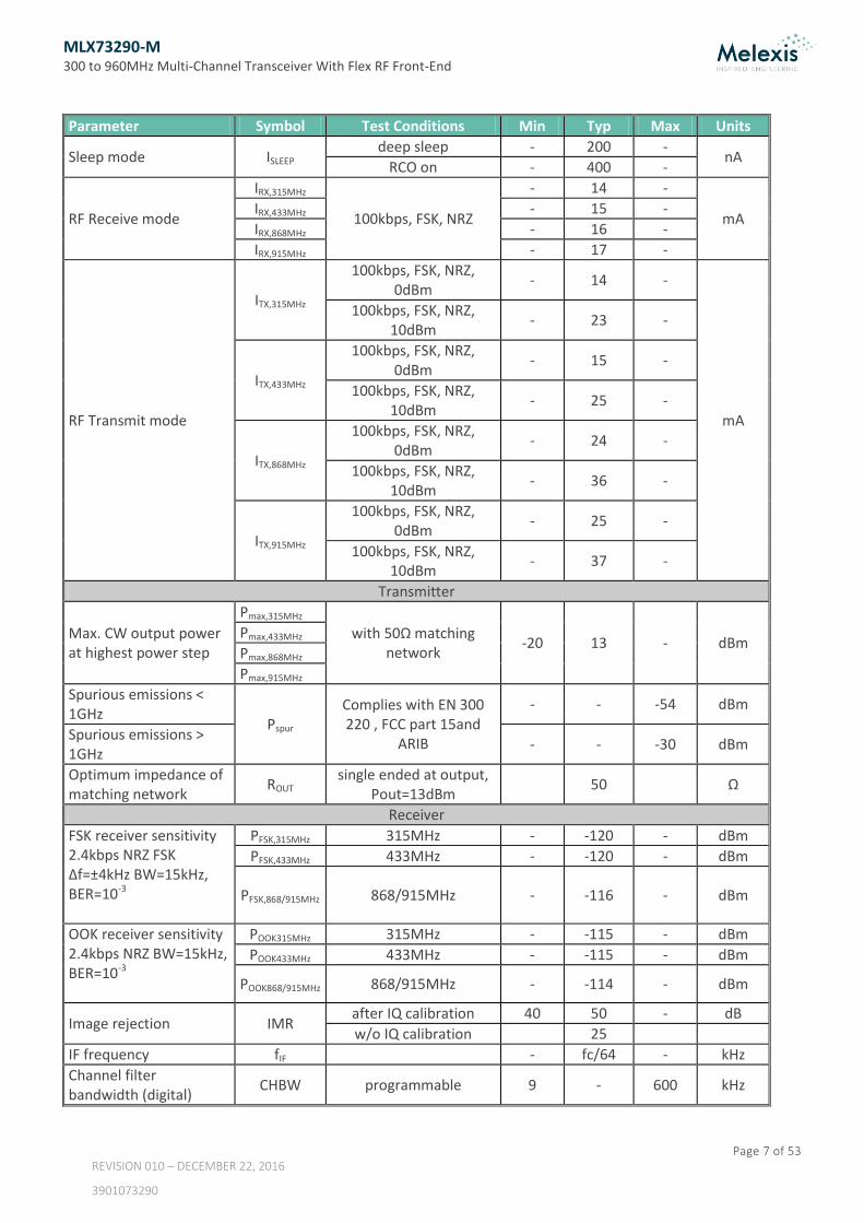
8.3. RF Characteristics
Operating Conditions: TA = -40oC to 105oC, VDD = 2.1V to 3.6V (unless otherwise specified) Typical values at TA = 25oC and , VDD = 3.0V
Parameter Symbol Test Conditions Min Typ Max Units
General
Frequency Range
fRF,band1 299 - 331
MHz fRF,band2 425 - 480
fRF,band3 reserved for future use - - -
fRF,band4 850 - 960
Operating currents
MLX73290-M 300 to 960MHz Multi-Channel Transceiver With Flex RF Front-End
Page 7 of 53
REVISION 010 – DECEMBER 22, 2016
3901073290
Parameter Symbol Test Conditions Min Typ Max Units
Sleep mode ISLEEP deep sleep - 200 -
nA RCO on - 400 -
RF Receive mode
IRX,315MHz
100kbps, FSK, NRZ
- 14 -
mA IRX,433MHz - 15 -
IRX,868MHz - 16 -
IRX,915MHz - 17 -
RF Transmit mode
ITX,315MHz
100kbps, FSK, NRZ, 0dBm
- 14 -
mA
100kbps, FSK, NRZ, 10dBm
- 23 -
ITX,433MHz
100kbps, FSK, NRZ, 0dBm
- 15 -
100kbps, FSK, NRZ, 10dBm
- 25 -
ITX,868MHz
100kbps, FSK, NRZ, 0dBm
- 24 -
100kbps, FSK, NRZ, 10dBm
- 36 -
ITX,915MHz
100kbps, FSK, NRZ, 0dBm
- 25 -
100kbps, FSK, NRZ, 10dBm
- 37 -
Transmitter
Max. CW output power at highest power step
Pmax,315MHz
with 50Ω matching network
-20 13 - dBm Pmax,433MHz
Pmax,868MHz
Pmax,915MHz
Spurious emissions < 1GHz
Pspur Complies with EN 300 220 , FCC part 15and
ARIB
- - -54 dBm
Spurious emissions > 1GHz
- - -30 dBm
Optimum impedance of matching network
ROUT single ended at output,
Pout=13dBm 50 Ω
Receiver
FSK receiver sensitivity 2.4kbps NRZ FSK ∆f=±4kHz BW=15kHz, BER=10-3
PFSK,315MHz 315MHz - -120 - dBm
PFSK,433MHz 433MHz - -120 - dBm
PFSK,868/915MHz 868/915MHz - -116 - dBm
OOK receiver sensitivity 2.4kbps NRZ BW=15kHz, BER=10-3
POOK315MHz 315MHz - -115 - dBm
POOK433MHz 433MHz - -115 - dBm
POOK868/915MHz 868/915MHz - -114 - dBm
Image rejection IMR after IQ calibration 40 50 - dB
w/o IQ calibration 25
IF frequency fIF - fc/64 - kHz
Channel filter bandwidth (digital)
CHBW programmable 9 - 600 kHz

MLX73290-M 300 to 960MHz Multi-Channel Transceiver With Flex RF Front-End
Page 8 of 53
REVISION 010 – DECEMBER 22, 2016
3901073290
Parameter Symbol Test Conditions Min Typ Max Units
Input intercept point IIP3 at max. gain -28 dBm
Adjacent channel rejection
ACR 9kHz CHBW, (G)FSK - 46 - dB
Blocking BLK
2MHz offset (50kHz CHBW)
- 52 - dB
10MHz offset (50kHz CHBW)
- 71 - dB
Timings
PA ramp up/down duration
programmable 0 - 192 μs
Channel switching time tswitch max frequency step - - 300 μs
RX/TX turn-around time ∆tRXTX - - 50 µs
Sleep to RX on time tRX programmable 200 - - µs
Sleep to TX on time tTX programmable 200 - - µs
Modulator and data rate
FSK deviation Δf Programmable in steps - - ±125 kHz
GFSK normalized BW BT fixed - 0.5 -
OOK modulation depth MOOK 100% modulation 70 80 - dB
Data rate DRFSK NRZ coding FSK 0.15 - 250 kbps
DROOK NRZ coding OOK 0.15 - 50 kbps
Synthesizer
Phase noise NPH_10kHz @ 10kHz offset - - -94 dBc/Hz
NPH_1MHz @ 1MHz offset - - -110 dBc/Hz
Frequency resolution fRES 57 61 65 Hz
RX/TX switching time ΔtRXTX - - 50 μs
RX or TX frequency change
- - 15 μs
Crystal oscillator
Crystal oscillator frequency
f0 30 32 34 MHz
Crystal oscillator start-up time
tROstart - 0.8 1 ms
Recommended crystal specification
Crystal frequency accuracy
Δf0 - - ±30 ppm
Load capacitance (differential)
CL Recommended for ext.
crystal 8 12 15 pF
Static capacitance C0 Recommended for ext.
crystal - - 5 pF
Maximum Drive Level MDL Recommended for ext.
crystal - - 100 μW
Equivalent series resistance (ESR)
R1 Recommended for ext.
crystal - - 70

MLX73290-M 300 to 960MHz Multi-Channel Transceiver With Flex RF Front-End
Page 9 of 53
REVISION 010 – DECEMBER 22, 2016
3901073290
8.4. SPI Characteristics
Operating Conditions: TA = -40oC to 105oC, VDD = 2.1V to 3.6V (unless otherwise specified)
Parameter Symbol Test Conditions Min Typ Max Units
SPI Clock Frequency fSCLK - 1 10 MHz
SCK high time tSCKH SCK ↑ to SCK ↓ 40 - - ns
SCK low time tSCKL SCK ↓ to SCK ↑ 40 - - ns
SCK period tSCK Between equal edges of SCK
100 - - ns
Setup time tSU CS and SDI stable to SCK ↑ 20 - - ns
Hold time tHD SCK ↑ to CS or SDI changing
20 - ns
SDO data delay tSDO SCK ↓ to SDO stable - 20 - ns
Output enable delay tOE SCK ↓ to SDO output enabled
- 20 - ns
Output disable delay tOD CS ↓ to SDO tri-state - 50 - ns
SCK ...
SDI
SDO
...
tSCKL tSCKH
...
tSCK
tSU
...
tOE tSDO
tHD
tOD
CS
Figure 3: SPI timing specifications
9. Functional Description
9.1. Frequencies and Standards
The MLX73290-M complies with the following frequency bands and radio standards.
freq. band [MHz]
max. ERP [dBm]
channel BW [kHz]
max. data rate [kbps]
Comment
300-330 -20 0.25% of center freq.
20 (OOK, FSK) SRDs - FCC 15.231 Japan ULP Band
426-469 433-434 446-447
10 10 10
12.5 - 25 not defined 25
5 (FSK) 200 (OOK, FSK) 1.2 (FSK)
Japan (ARIB), Korea SRDs - EN 300 220, DASH7 Europe PMR, US FSR
863-870 902-928
14 -1
25 - 600 200 (typ.)
250 (OOK, FSK) 250 (OOK, FSK)
SRDs - EN 300 220 SRDs - FCC 15.249
MLX73290-M 300 to 960MHz Multi-Channel Transceiver With Flex RF Front-End
Page 10 of 53
REVISION 010 – DECEMBER 22, 2016
3901073290
9.2. Block Diagram
2
2
TX AM / Bias
4
MOD Ramp up/dnFM
AM
RF DSPAGC AFC
Filter
DAC
Detector
Power
Detector
Power DAC
LNA IQ Mixer
RF2P,RF2N
RF1P,RF1N
SPI
CS
SCK
SDI
SDO
PD1
Co
ntr
ol
+ s
tatu
s r
eg
iste
rs
PGA
RF
RX
FIF
OR
F T
X F
IFO
synthesis
Frequency
256 bytes
PA
XTALP
XTALN
GP
IO_M
UX
GPIO[3:0]
PD2
ADC
General
purpose ADC
Service
blocksMU
XM
UX
REF
Demod + CDR Deserializer
Serializer
Clock
RF state machine
Power control
Timers
VDDD3VMAINVHARV
Power switch
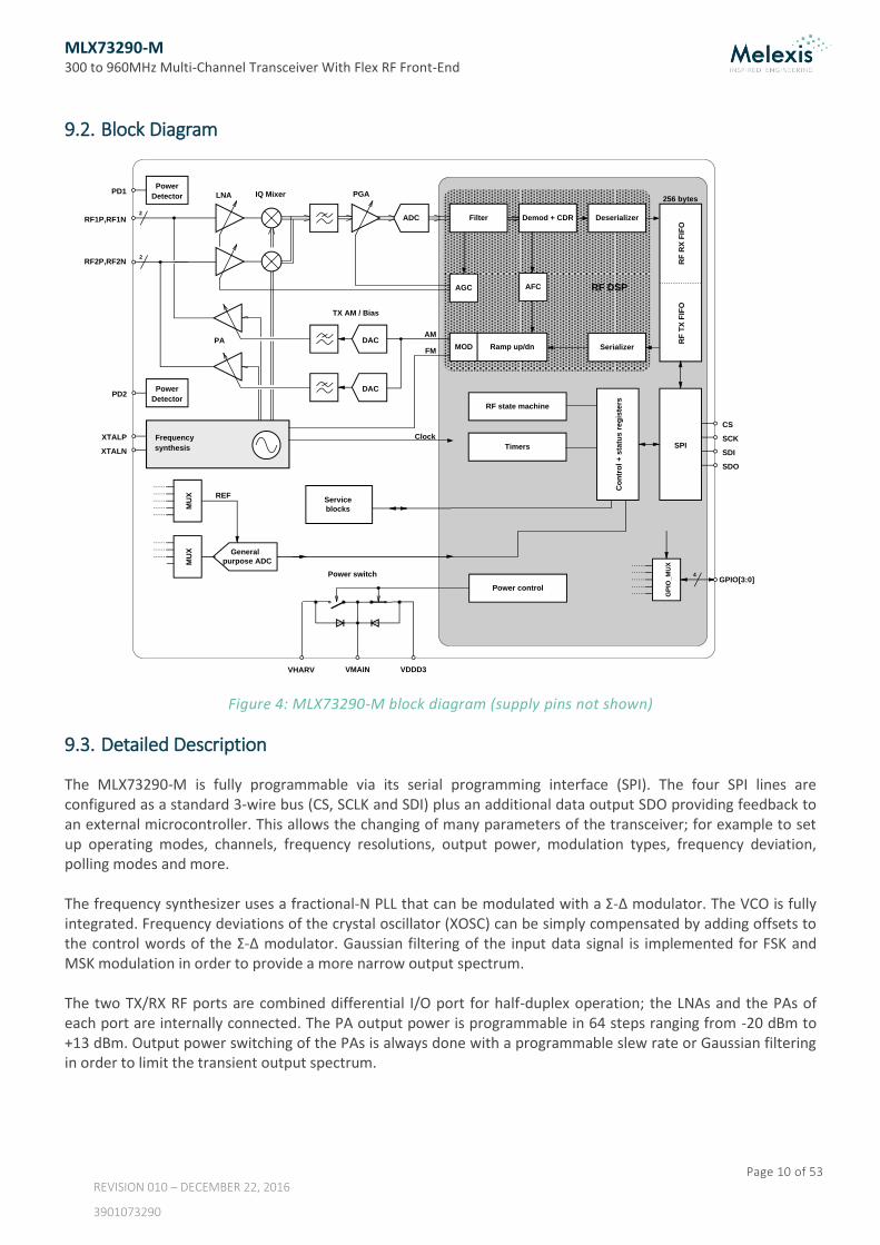
Figure 4: MLX73290-M block diagram (supply pins not shown)
9.3. Detailed Description
The MLX73290-M is fully programmable via its serial programming interface (SPI). The four SPI lines are configured as a standard 3-wire bus (CS, SCLK and SDI) plus an additional data output SDO providing feedback to an external microcontroller. This allows the changing of many parameters of the transceiver; for example to set up operating modes, channels, frequency resolutions, output power, modulation types, frequency deviation, polling modes and more. The frequency synthesizer uses a fractional-N PLL that can be modulated with a Σ-Δ modulator. The VCO is fully integrated. Frequency deviations of the crystal oscillator (XOSC) can be simply compensated by adding offsets to the control words of the Σ-Δ modulator. Gaussian filtering of the input data signal is implemented for FSK and MSK modulation in order to provide a more narrow output spectrum. The two TX/RX RF ports are combined differential I/O port for half-duplex operation; the LNAs and the PAs of each port are internally connected. The PA output power is programmable in 64 steps ranging from -20 dBm to +13 dBm. Output power switching of the PAs is always done with a programmable slew rate or Gaussian filtering in order to limit the transient output spectrum.

MLX73290-M 300 to 960MHz Multi-Channel Transceiver With Flex RF Front-End
Page 11 of 53
REVISION 010 – DECEMBER 22, 2016
3901073290
A low voltage detector disconnects the RF signal from the PAs if the supply voltage drops below a certain threshold value. This prevents the transmission of undesired frequencies at the battery’s end of life. In order to minimize the load of the host MCU, a packet handler takes care of formatting/pre-processing the data in both Receive & Transmit mode. An on-chip power switch selects the supply voltage either from the battery (VDDA3) or from the energy-harvesting input (VHARV). It also provides the supply for the external host MCU (VMAIN). Self-polling is realized by an integrated timer with very low power consumption. The polling mode wakes up the receiver or transmitter after a programmable time and scans one or more frequency channels for valid data. It can also be used to transmit the same data in a periodic way. A transparent transmit or receive mode can also be chosen by selecting clock and data on GPIO pins.
9.4. RF Transceiver
The MLX73290-M is compliant with EN 300 220, FCC part 15 and ARIB STD-67 standards. It also supports DASH7 modes 1 and 2, as well as proprietary OOK, (G)MSK and (G)FSK-modulated communication protocols in ISM and SRD applications between 300 and 960MHz. Data rates between 0.15 and 250kbps, FSK deviations of up to 125kHz and RF output power levels between -20dBm and +13dBm can be used.
9.4.1. Flex TX/RX Front-End
The RF front-end consists of two differential TX/RX ports for half-duplex operation. Possible configurations are described below.
Low-cost, single-antenna TX/RX configuration
RF port 1 is connected to a single antenna through a matching network (MNW)
LNA1 is active in RX mode only
PA1 is active in TX mode only
Power detector 1 can be used for sensing the power at the antenna
PA2, LNA2 and power detector 2 are not used
Figure 5
2
2
PWRDET
2
RF2P
RF2N
RF1P
RF1N
PD2
PA1
PA2
LNA1
LNA2
PWRDET
1PD1
MNW
antenna

MLX73290-M 300 to 960MHz Multi-Channel Transceiver With Flex RF Front-End
Page 12 of 53
REVISION 010 – DECEMBER 22, 2016
3901073290
High-end, single-antenna TX/RX configuration
RF port 1 operates in RX mode only
RF port 2 operates in TX mode only
RF port 2 connects to an external PA for boosting the TX power (e.g. up to 20dBm)
RF port 1 and external PA output are connected to one antenna through a MNW
External PA can be turned on/off via a GPIO pin
Power detector 1 can be used for sensing the power at the antenna
Figure 6
2
2
PWRDET
2
RF2P
RF2N
RF1P
RF1N
PD2
PA1
PA2
LNA1
LNA2
PWRDET
1PD1
PAext
MNW
antenna
GPIO
on/off
Antenna space or frequency diversity configuration
RF port 1 is connected to antenna 1
RF port 2 is connected to antenna 2
the two RF ports operate at the same frequency
→ antenna space diversity
the two RF ports operate at different frequencies
→ frequency diversity
Power detectors 1 and 2 can be used for sensing the power at the antennas
Figure 7
2
2
PWRDET
2
RF2P
RF2N
RF1P
RF1N
PD2
PA1
PA2
LNA1
LNA2
PWRDET
1PD1
MNW 1
antenna 1
MNW 2
antenna 2

MLX73290-M 300 to 960MHz Multi-Channel Transceiver With Flex RF Front-End
Page 13 of 53
REVISION 010 – DECEMBER 22, 2016
3901073290
9.4.2. Frequency Synthesizer
At the analog heart of the RF transceiver is a frequency synthesizer based on a Sigma-Delta fractional-N PLL. From a typical 32MHz crystal reference clock, the PLL derives a quadrature LO-signal used for the mixers in the receive mode and to generate the carrier frequency in transmit mode. The PLL division ratio consists of a 6-bit integer part and a 19-bit fractional part, yielding to a resolution of 60Hz. The VCO of the PLL requires to be calibrated; for this purpose a calibration algorithm is implemented in the digital domain of the MLX73290-M device.
9.4.3. Transmit Mode (TX)
In RF transmit mode, the MLX73290-M outputs a CW signal on the two differential RF outputs RFP and RFN. The output power of the two PAs can be configured from -20dBm to 13dBm by the control bits RFTX_PWR1 and RFTX_PWR2 with the following tuning range:
bits [7:6] for selecting the output stages 1 to 4,
bits [5:3] for selecting the octave range (octave 000 = power OFF, 111 = power saturation),
bits [2:0] for linear power tuning.
The frequency of the CW signal can be adjusted with the bits CENTER_FREQ[24:0] according to the formula below.
The RF transmit band has to be selected accordingly with the bits BAND_SEL[1:0]. A packet handler reads data stored into the RFTX_FIFO to construct an RF packet including the programmable preamble, the synchronization word, a fixed or variable length of payload (up to 255 bytes), an optional address byte, and an optional CRC-16 checksum inserted at the end. The serializer block supports the specific data formats of IEEE 802.15.4 and DASH7 mode 2. The bit order (LSB or MSB first) and bit polarity are configurable. After optional data whitening and Manchester encoding, the data stream of the serialized RF packet enters the OOK or FSK modulator. In case of OOK modulation, the PLL-based frequency synthesizer is programmed to the wanted carrier frequency and the power amplifier (PA) is switched ON and OFF. In case of FSK modulation, the data stream is converted to a frequency deviation programmable between 0 and 125 kHz. The FSK signal directly modulates the PLL of the frequency synthesizer. For both OOK and FSK modulation, the data stream can be selected with optional Gaussian pulse shaping (EN_GAUSSIAN) to reduce the spectral bandwidth of the transmitted RF signal.
9.4.4. Receive Mode (RX)
The receiver chain features an IQ receiver topology. The RF signal is converted to the low IF band by an image reject mixer (the IF is at 500kHz). In order to address a wide dynamic range, the LNA as well as the programmable gain amplifier (PGA) conditions the IF signal. An automatic gain control loop ensures a stable signal level at the
MLX73290-M 300 to 960MHz Multi-Channel Transceiver With Flex RF Front-End
Page 14 of 53
REVISION 010 – DECEMBER 22, 2016
3901073290
input of the ADC which translates the signal to the digital domain. The base-band signal path features digital channel filtering, demodulation and extraction of clock and data. A de-serializer is used for extracting the payload from an incoming packet and it writes the payload to a FIFO that can be read out by the SPI. A packet handler scans the demodulated signal for valid bit pattern followed by a programmable synchronization word of 16, 24 or 32 bits (SYNC_WORD[31:0] and SYNC_WORD_LEN[1:0]) and a fixed or variable length of payload (RFRX_FIFO of up to 255 bytes). An optional de-whitening operation as well as CRC-16 checksum verification could be enabled to reduce the load of the external host microcontroller.
9.4.4.1. Automatic Receiver Polling
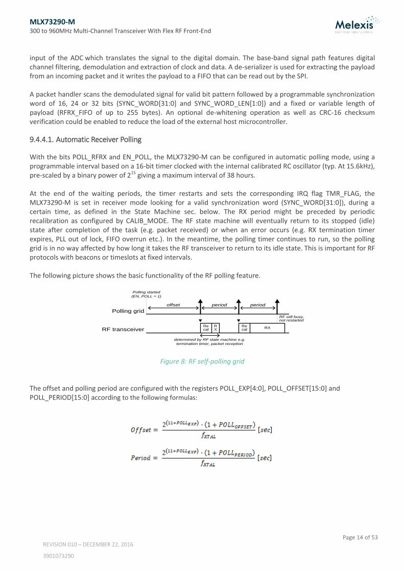
With the bits POLL_RFRX and EN_POLL, the MLX73290-M can be configured in automatic polling mode, using a programmable interval based on a 16-bit timer clocked with the internal calibrated RC oscillator (typ. At 15.6kHz), pre-scaled by a binary power of 215 giving a maximum interval of 38 hours. At the end of the waiting periods, the timer restarts and sets the corresponding IRQ flag TMR_FLAG, the MLX73290-M is set in receiver mode looking for a valid synchronization word (SYNC_WORD[31:0]), during a certain time, as defined in the State Machine sec. below. The RX period might be preceded by periodic recalibration as configured by CALIB_MODE. The RF state machine will eventually return to its stopped (idle) state after completion of the task (e.g. packet received) or when an error occurs (e.g. RX termination timer expires, PLL out of lock, FIFO overrun etc.). In the meantime, the polling timer continues to run, so the polling grid is in no way affected by how long it takes the RF transceiver to return to its idle state. This is important for RF protocols with beacons or timeslots at fixed intervals. The following picture shows the basic functionality of the RF polling feature.
RF transceiver
Polling grid
Polling started
(EN_POLL = 1)
offset period period
Recal
RX
Recal
RX
RF still busy,not restarted
determined by RF state machine e.g.
termination timer, packet reception
Figure 8: RF self-polling grid
The offset and polling period are configured with the registers POLL_EXP[4:0], POLL_OFFSET[15:0] and POLL_PERIOD[15:0] according to the following formulas:

MLX73290-M 300 to 960MHz Multi-Channel Transceiver With Flex RF Front-End
Page 15 of 53
REVISION 010 – DECEMBER 22, 2016
3901073290
9.4.4.2. RSSI Information
RSSI information is available for the user in the register RSSI_HDR[6:0] which contains the RSSI information measured just after a valid Header is detected.
9.4.4.3. Carrier Frequency Acceptance Range
With its carrier recovery feature the MLX73290-M is able to tolerate a carrier frequency range of up to ±2·DR, with DR being the raw data rate. The carrier frequency acceptance range (CFAR) does not depend on the AFC setting. The AFC just enables the carrier recovery to converge packet after packet to a given value. This potentially allows the preamble length to be reduced, if losing a few packets at the beginning is tolerated. Fig. 9 illustrates the packet error rate (PER) vs CFAR. The example here is given for DR = 55.6kbps with a ±50kHz FSK modulation. As can be seen, that there is a tradeoff between the preamble length (which is the part of the packet during which the carrier recovery tries to converge) and the PER.
Figure 9: CFAR (Δf) at different preamble lengths
MLX73290-M 300 to 960MHz Multi-Channel Transceiver With Flex RF Front-End
Page 16 of 53
REVISION 010 – DECEMBER 22, 2016
3901073290
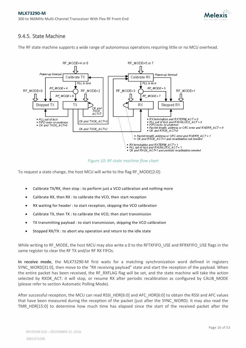
9.4.5. State Machine
The RF state machine supports a wide range of autonomous operations requiring little or no MCU overhead.
Figure 10: RF state machine flow chart To request a state change, the host MCU will write to the flag RF_MODE[2:0]:
Calibrate TX/RX, then stop : to perform just a VCO calibration and nothing more
Calibrate RX, then RX : to calibrate the VCO, then start reception
RX waiting for header : to start reception, skipping the VCO calibration
Calibrate TX, then TX : to calibrate the VCO, then start transmission
TX transmitting payload : to start transmission, skipping the VCO calibration
Stopped RX/TX : to abort any operation and return to the idle state
While writing to RF_MODE, the host MCU may also write a 0 to the RFTXFIFO_USE and RFRXFIFO_USE flags in the same register to clear the RF TX and/or RF RX FIFOs. In receive mode, the MLX73290-M first waits for a matching synchronization word defined in registers SYNC_WORD[31:0], then move to the “RX receiving payload” state and start the reception of the payload. When the entire packet has been received, the RF_RXFLAG flag will be set, and the state machine will take the action selected by RXOK_ACT: it will stop, or resume RX after periodic recalibration as configured by CALIB_MODE (please refer to section Automatic Polling Mode). After successful reception, the MCU can read RSSI_HDR[6:0] and AFC_HDR[6:0] to obtain the RSSI and AFC values that have been measured during the reception of the packet (just after the SYNC_WORD). It may also read the TMR_HDR[15:0] to determine how much time has elapsed since the start of the received packet after the
MLX73290-M 300 to 960MHz Multi-Channel Transceiver With Flex RF Front-End
Page 17 of 53
REVISION 010 – DECEMBER 22, 2016
3901073290
SYNC_WORD detection, which is particularly useful in slotted protocols, where the next transmission or reception should start at a certain distance relative to the beginning of the received packet. If a CRC and/or address check is enabled, and the packet gets rejected on that basis, RXERR_ACT will determine whether the state machine will stop and report a CRC or address error, or flush the RF RX FIFO and resume the reception. Furthermore there is the option to set a threshold RX_RSSI_TH on the RSSI, below which reception is inhibited, and there is a termination timer programmable between 64µs and 32s (RXTERM_MANT[3:0] and RXTERM_EXP[3:0]). When the timer expires, termination may be postponed while RSSI is above the threshold, or while payload is being received, depending on the setting of the bit RXTERM_COND. Then the state machine will take the action selected by RXTERM_ACT: it will stop or recalibrate and resume reception. When the PLL gets out of lock, depending on RXUNLOCK_ACT the state machine will stop and report a PLL out-of-lock error or it will take the same actions as for termination. When there is an overrun/underrun on the RFRXFIFO, the state machine will stop and report a FIFO overrun/underrun error (RFRX_FIFO_USE) which can also be output on one GPIO. Important Note: To enable the RF RX functionality, the register RF_BIAS[7:0] in Bank 0 has to be set to 0x4C for the 315MHz band, to 0x63 for the 433MHz band and to 0x99 for the 868MHz and 915MHz bands.
In transmit mode, after transmission of the payload, the state machine will, depending on TXOK_ACT, stop, resume TX after periodic recalibration as configured by CALIB_MODE, or, after optional calibration, enter RX mode. When DIRECT_MOD > 2 direct modulation with a fixed logic 0 or 1 level, or from one of the GPIO digital input pins is selected. In this case the data-handler is bypassed and it is the responsibility of the microcontroller to terminate the transmission by changing RF_MODE. This mode will allow for the transmission of un-modulated as well as modulated carriers for characterization, test and type approval. A clock at the programmable symbol rate can be output on one of the GPIO pins for transmission of a synchronous bit stream. When the PLL gets out-of-lock during transmission, the state machine will always abort and report a PLL out of-lock error (PLL_LOCKED). When there is an overrun/underrun on the RFTXFIFO, the state machine will stop and report a FIFO overrun/underrun error (RFTX_FIFO_USE).
By putting KEEP_PLL_ON to ‘1’, the PLL can be kept running regardless the state of the RF transceiver, this is particularly useful for protocols where transmission or reception is triggered by an event and the normal startup delay of the PLL cannot be tolerated.
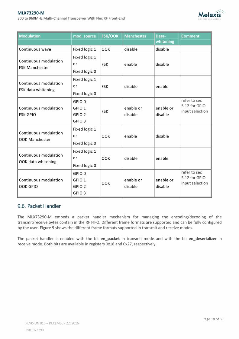
9.5. Modulation Settings
The below table provides an overview on the modulation settings. Continuous modulation can also be applied through the GPIOs. In this case the selected GPIO pin must be set as a digital input.
MLX73290-M 300 to 960MHz Multi-Channel Transceiver With Flex RF Front-End
Page 18 of 53
REVISION 010 – DECEMBER 22, 2016
3901073290
Modulation mod_source FSK/OOK Manchester Data-whitening
Comment
Continuous wave Fixed logic 1 OOK disable disable
Continuous modulation
FSK Manchester
Fixed logic 1
or
Fixed logic 0
FSK enable disable
Continuous modulation
FSK data whitening
Fixed logic 1
or
Fixed logic 0
FSK disable enable
Continuous modulation
FSK GPIO
GPIO 0
GPIO 1
GPIO 2
GPIO 3
FSK enable or
disable
enable or
disable
refer to sec 5.12 for GPIO input selection
Continuous modulation
OOK Manchester
Fixed logic 1
or
Fixed logic 0
OOK enable disable
Continuous modulation
OOK data whitening
Fixed logic 1
or
Fixed logic 0
OOK disable enable
Continuous modulation
OOK GPIO
GPIO 0
GPIO 1
GPIO 2
GPIO 3
OOK enable or
disable
enable or
disable
refer to sec 5.12 for GPIO input selection
9.6. Packet Handler
The MLX73290-M embeds a packet handler mechanism for managing the encoding/decoding of the transmit/receive bytes contain in the RF FIFO. Different frame formats are supported and can be fully configured by the user. Figure 9 shows the different frame formats supported in transmit and receive modes. The packet handler is enabled with the bit en_packet in transmit mode and with the bit en_deserializer in receive mode. Both bits are available in registers 0x18 and 0x27, respectively.

MLX73290-M 300 to 960MHz Multi-Channel Transceiver With Flex RF Front-End
Page 19 of 53
REVISION 010 – DECEMBER 22, 2016
3901073290
Figure 11: Packet handler - frame formats
9.6.1. Preamble
A preamble can be automatically added to the packet structure even if it is completely handled by the host MCU. This feature can be turned on by simply setting the bit en_preamble signal to 1. The length of the preamble is given by the signal pattern_world_len[1:0] (number of times that the preamble byte is repeated) and the preamble itself is given by the preamble[7:0] in bank 0 (by default to 0x55).
9.6.2. Sync Word
The synchronization word is introduced automatically if the preamble is present. The length of the sync word is given by the sync_word_len. The synchronization word is always sent LSB first.
9.6.3. Packet Length
If the packet handler is enabled, it has to know the length of the packet to be sent/received. This one can be fixed or variable depending on the user settings. If the fixed solution is chosen, the en_packet_len_fix has to be set to 1. In this case the length of the packet is given by the byte packet_len[7:0]. In the case of a variable packet length (en_packet_len_fix set to 0), the length is normally specified as one of the first bytes of the packet. The byte packet_len_pos[1:0] specify the position of this byte (e.g. if set to 0, means that the first byte sent/received is defining the packet length). The packet handler always considers the length of the packet from the first byte after the packet length byte until the last byte before the CRC. The bit packet_len_corr specify the correction to apply to the packet length. This gives the possibility for the user to provide/receive frame format with a length byte including itself and/or is included in the CRC computation. The following picture shows the packet_len_corr principle.
bytes
Preamble 0 to 256
Sync word 16, 28 or 32
bits Length
byte Address
byte up to 255 bytes Message CRC16
2 bytes Protocol
ID
en_packet_len_fix=0 packet_len_pos=1 en_address=1 en_crc=1
bytes
Preamble 0 to 256
Sync word 16, 28 or 32
bits Length
byte Address
byte up to 255 bytes Message CRC16
2 bytes
en_packet_len_fix=0 packet_len_pos=0 en_address=1 en_crc=1
bytes
Preamble 0 to 256
Sync word 16, 28 or 32
bits Length
byte up to 255 bytes Message CRC16
2 bytes
en_packet_len_fix=0 packet_len_pos=0 en_address=0 en_crc=1
bytes
Preamble 0 to 256
Sync word 16, 28 or 32
bits Length
byte up to 255 bytes Message
en_packet_len_fix=0 en_address=0 en_crc=0
bytes
Preamble 0 to 256
Sync word 16, 28 or 32
bits up to 255 bytes Message
en_packet_len_fix=1
en_crc=0 en_address=0
MLX73290-M 300 to 960MHz Multi-Channel Transceiver With Flex RF Front-End
Page 20 of 53
REVISION 010 – DECEMBER 22, 2016
3901073290
Figure 12: Packet handler - packet correction principle
9.6.4. Address
An address can be inserted automatically after the packet length if the bit en_address is set to 1. The address is given by the byte address[7:0].
9.6.5. CRC16
A checksum CRC16 can be automatically computed and added/compared to the packet sent/received, by setting the bit en_crc to 1. In case of reception, the status bits rfrx_flag and rf_info[2:0] will be automatically updated in case of CRC error.
9.6.6. Multi Frame
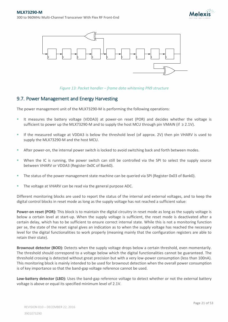
If the en_multi_frame bit is set to 1, the multi-frame mode is enabled. A frame is composed by the data and the corresponding CRC. In this mode, a preamble and a single synchronization word are followed by multiple frames. As long as the en_multi_frame bit is set to 1, the packet handler continues to send/receive frames.
5.5.7 Data Whitening
The packet handler also includes a data whitening process during the transmission or the reception of RF packets. In this case, all the data to be sent/received are encoded/decoded using a PN9 polynomial of X9+X5+1. The data-whitening process is illustrated in the picture below. The data whitening process is enabled with the bit en_white.
bytes
Preamble
0 to 256
Sync word
8, 16 or 32
bits
Length
byte
Address
byte
CRC16
2 bytes
Protocol
ID
Byte
#1
Byte
#2
packet_len_corr=0length byte = 3
length byte = 5
length byte = 7
length byte = 5
packet_len_corr=-2
packet_len_corr=-2
packet_len_corr=-4
MLX73290-M 300 to 960MHz Multi-Channel Transceiver With Flex RF Front-End
Page 21 of 53
REVISION 010 – DECEMBER 22, 2016
3901073290
Figure 13: Packet handler – frame data whitening PN9 structure
9.7. Power Management and Energy Harvesting
The power management unit of the MLX73290-M is performing the following operations: It measures the battery voltage (VDDA3) at power-on reset (POR) and decides whether the voltage is
sufficient to power up the MLX73290-M and to supply the host MCU through pin VMAIN (if ≥ 2.1V). If the measured voltage at VDDA3 is below the threshold level (of approx. 2V) then pin VHARV is used to
supply the MLX73290-M and the host MCU. After power-on, the internal power switch is locked to avoid switching back and forth between modes. When the IC is running, the power switch can still be controlled via the SPI to select the supply source
between VHARV or VDDA3 (Register 0x0C of Bank0). The status of the power management state machine can be queried via SPI (Register 0x03 of Bank0). The voltage at VHARV can be read via the general purpose ADC. Different monitoring blocks are used to report the status of the internal and external voltages, and to keep the digital control blocks in reset mode as long as the supply voltage has not reached a sufficient value: Power-on reset (POR): This block is to maintain the digital circuitry in reset mode as long as the supply voltage is below a certain level at start-up. When the supply voltage is sufficient, the reset mode is deactivated after a certain delay, which has to be sufficient to ensure correct internal state. While this is not a monitoring function per se, the state of the reset signal gives an indication as to when the supply voltage has reached the necessary level for the digital functionalities to work properly (meaning mainly that the configuration registers are able to retain their state). Brownout detector (BOD): Detects when the supply voltage drops below a certain threshold, even momentarily. The threshold should correspond to a voltage below which the digital functionalities cannot be guaranteed. The threshold crossing is detected without great precision but with a very low-power consumption (less than 100nA). This monitoring block is mainly intended to be used for brownout detection when the overall power consumption is of key importance so that the band-gap voltage reference cannot be used. Low-battery detector (LBD): Uses the band-gap reference voltage to detect whether or not the external battery voltage is above or equal its specified minimum level of 2.1V.
MLX73290-M 300 to 960MHz Multi-Channel Transceiver With Flex RF Front-End
Page 22 of 53
REVISION 010 – DECEMBER 22, 2016
3901073290
9.8. Programmable Timer / Clock Generator
A programmable timer / clock generator may periodically wake up the host MCU or it can provide a clock signal, derived from the RC oscillator, the calibrated RC clock or the crystal clock. A prescaler first divides the selected clock source by a programmable binary power between 1 and 231, and then by an 8-bit linear division ratio between 1 and 256. The timer period is configured with the bits TMR_MANT[7:0] and TMR_EXP[4:0]. The following formula can be used to calculate the timer period, relative to the clock source selected by the bits TMR_SOURCE[1:0]:
[sec]
The timer can be selected in Timer or Clock mode with the bit TMR_MODE. In Timer mode, the timer stops when the flag gets set, and the MCU must clear the flag to restart the timer. In Clock mode, the timer is continuously running thus providing a reference clock for the host MCU. The timer is, by default configured to output the RC oscillator clock signal on GPIO2 without any division (i.e. ratio 1:1) so that it may act as a clock signal for the MCU. There is also the possibility to configure the timer output to another GPIO. For more information about the programmable timer, please refer to section 10.4.
9.9. System Timer
The MLX73290-M embeds a 23-bit free-running counter that can serve as a time reference. When enabled, it increments at 7.8 kHz derived from the calibrated RC clock. Counter overflows (every ~18 minutes) will set a flag, which may wake-up the microcontroller. The firmware can then clear the flag and increment a counter in the microcontroller to extend the counter range to any length. To determine the elapsed time between two events, take a snapshot of this free-running system time at both moments and subtract these two values to find the elapsed time with 128 µs resolution. For more information about the system timer, please refer to section 10.4.
9.10. General Purpose ADC
The external host MCU can use a built-in 10-bit general purpose ADC to measure several internal signals selected with the bits ADC_CH_SEL[3:0] (e.g. supply voltages, output of the RF power detectors, 3D LF field strength, temperature sensor, analog level of one of the GPIO pins). The ADC can be configured for continuous sampling or a single measurement (ADC_CONTINU bit set). The conversion clock can be set to 1/16th, 1/32nd or 1/64th of the crystal clock (ADC_CLK_SEL[1:0]), corresponding
to a period of conversion of respectively tAD = 0.5, 1 or 2 s with a 32MHz crystal. A full conversion cycle takes
128 clocks leading to a conversion time of 64, 128 or 256 s, resulting in 16, 8 or 4 kS/s throughput. The conversion is started with the bit ADC_START_EOC and the result stored into the register ADC_CAL[9:0]. Since the conversion results are 10 bit wide, the microcontroller will need to read them as 2 bytes through the SPI interface. This is an asynchronous process, so when the ADC operates in continuous sampling mode, the
MLX73290-M 300 to 960MHz Multi-Channel Transceiver With Flex RF Front-End
Page 23 of 53
REVISION 010 – DECEMBER 22, 2016
3901073290
completion of a new conversion may coincide with the retrieval of the 2 bytes of the results of the previous conversion. Without special provisions the microcontroller may receive the first byte of the old conversion and the second byte of the new conversion, which could give a false reading. To prevent such inconsistencies, the generic ADC therefore takes a snapshot of the conversion results when the first byte is read, and returns the second part of the snapshot when the second byte is read in the same (burst mode) read access. The generic ADC maintains a flag, ADC_NEWDATA, to indicate whether new results are available, primarily intended for continuous sampling mode. The completion of a conversion will set the flag, and reading the first byte of the results will clear the flag. The microcontroller may poll this flag to check if a new sample is available, and if so, it may continue reading the two byte result, which will clear the flag.
9.11. SPI Communication
The serial programming interface (SPI) is composed of three inputs and one output as shown in the following table.
SPI pin I/O Description
CS input SPI Chip Select active high
SDO output SPI Slave data output
SDI input SPI Slave data input
SCK input SPI Clock
The SDO pin is set high impedance by the MLX73290-M when not transmitting SPI information; this allows a configuration using only one pin to successively send/receive information from/to the MLX73290-M. The two configurations using classical 4-pin and optimized 3-pin are illustrated below:
MLX
73290MCU
CS
SCK
SDI
SDO
CS
SCK
SDO
SDI
MLX
73290MCU
CS
SCK
SDI
SDO
CS
SCK
SDIO
4-wire SPI 3-wire SPI
Figure 14: SPI connections
In Read mode, the serial data changes on the falling edges of the serial clock and is latched, during write mode, on the rising clock edges. Data are transmitted MSB first.
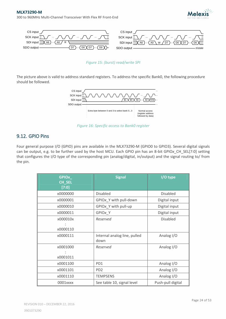
Opposite to most conventional SPI devices, the CS chip select input of the MLX73290-M is active high. When the CS is set low, the MLX73290-M is deselected as SPI-slave; SCK and SDI can take any level, and SDO is tri-state. When CS goes high, the MLX73290-M becomes selected, and expects from the host MCU, a 7-bit register address preceded by one bit of direction (0 = write, 1 = read). A so-called Burst mode is implemented in the MLX73290-M which automatically increment the address of the current register to be read/write. This operation is illustrated in the picture below:
MLX73290-M 300 to 960MHz Multi-Channel Transceiver With Flex RF Front-End
Page 24 of 53
REVISION 010 – DECEMBER 22, 2016
3901073290
SCK input ...
SDI input
... ...
SDO output ... ...D7 D0 D7 D0
CS input
... RA6 A0
CS input
SCK input ...
SDI input
... ...
... ...
SDO output
... WA6 A0 D7 D0 D7 D0
tristate
Figure 15: (burst) read/write SPI
The picture above is valid to address standard registers. To address the specific Bank0, the following procedure should be followed.
Extra byte between 0 and 3 to select bank 0...3 Normal access
(register address
followed by data)
SCK input
SDI input
SDO output
CS input
B0B1
...
... R/WA6 A0 ...
...
...
...
Figure 16: Specific access to Bank0 register
9.12. GPIO Pins
Four general purpose I/O (GPIO) pins are available in the MLX73290-M (GPIO0 to GPIO3). Several digital signals can be output, e.g. to be further used by the host MCU. Each GPIO pin has an 8-bit GPIOx_CH_SEL[7:0] setting that configures the I/O type of the corresponding pin (analog/digital, in/output) and the signal routing to/ from the pin.
GPIOx_ CH_SEL
[7:0]
Signal I/O type
x0000000 Disabled Disabled
x0000001 GPIOx_Y with pull-down Digital input
x0000010 GPIOx_Y with pull-up Digital input
x0000011 GPIOx_Y Digital input
x000010x :
x0000110
Reserved Disabled
x0000111 Internal analog line, pulled down
Analog I/O
x0001000 :
x0001011
Reserved Analog I/O
x0001100 PD1 Analog I/O
x0001101 PD2 Analog I/O
x0001110 TEMPSENS Analog I/O
0001xxxx See table 10, signal level Push-pull digital
MLX73290-M 300 to 960MHz Multi-Channel Transceiver With Flex RF Front-End
Page 25 of 53
REVISION 010 – DECEMBER 22, 2016
3901073290
001xxxxx 01xxxxxx
inverted when GPIOx_CH_SEL[0] = 1
output
1001xxxx 101xxxxx 11xxxxxx
See table 10,signal level inverted when GPIOx_CH_SEL[0] = 1
Open collector digital output
The default values of GPIOs after power-on reset (POR) are:
GPIO0 : READY
GPIO1 : READY_NOT
GPIO2 : TMR_FLAG
GPIO3 : BATTOK
The digital signals are active high (unless otherwise specified). For GPIOx as digital output, the following truth table applies:
GPIOx_CH_SEL[6:1]
Signal Name Description
001000 Fixed logic 0
001001 READY MLX73290-M is ready after start-up sequence (POR)
001010 BATTOK Battery level measured above the minimum level 2.1V.
001011 RCO Output of un-calibrated internal RC oscillator
010100 LOWBAT Output of low battery detector on VDDA3
010101 XTAL_RDY Crystal clock is present and stable
011000 ADC_NEWDATA New result from general purpose ADC available
011001 SYS_TIME_OVF Internal system timer overflow
011010 TMR_FLAG Programmable timer flag
011011 POLL_FLAG RF Polling timer flag
011100 PLL_CYCLE_SLIP A PLL cycle-slip has been registered since the last read from this register
011101 PLL_IN_LOCK PLL successfully locked
011110 RFRX_CLK RF Clock output after data-handler
011111 RFRX_DATA RF Data output after data-handler
100000 RFRX_WAIT_HDR RF state-machine waiting for valid Header
100001 RFRX_PAYLOAD RF state-machine receiving the payload
100010 RFRX_WAIT_HDR_PAYLOAD RF state-machine waiting for valid Header or receiving Payload
100011 RFTX_PAYLOAD RF state-machine transmitting payload
100100 RF_STOPPED RF state-machine stopped (RX or TX)
100101 RF_STOPPED_ERR RF state-machine stopped with an error (RX or TX)

MLX73290-M 300 to 960MHz Multi-Channel Transceiver With Flex RF Front-End
Page 26 of 53
REVISION 010 – DECEMBER 22, 2016
3901073290
GPIOx_CH_SEL[6:1]
Signal Name Description
100110 RFTX_FIFO_OVRUDR RF TX FIFO overrun/underrun error
100111 RFRX_FIFO_OVRUDR RF RX FIFO overrun/underrun error
101000 RFRX_FIFO_1BYTE RF RX FIFO contains at least 1byte
101001 RFRX_FIFO_64BYTES RF RX FIFO contains at least 64bytes
101010 RFTX_FIFO_1BYTE RF TX FIFO contains at least 1byte
101011 RFTX_FIFO_64BYTES RF TX FIFO contains at least 64bytes
101100 RFTX_SYM_CLK RF TX Manchester symbol clock
101101 RFRX_RSSI_ABOVE_THR RX RSSI measured above threshold
101110 RFRX_PKT RF Data-handler packet received
10. Register Settings
The MLX73290-M is addressed through a set of 126 unbanked registers for standard use (addresses from 0x02 to 0x7F). One additional bank of 128 registers (Bank 0) is also available for specific information (addresses from 0x00 to 0x7F).
10.1. RF Transceiver (0x02 to 0x33)
Addr bit 7 bit 6 bit 5 bit 4 bit 3 bit 2 bit 1 bit 0
RF Transceiver
02 TMR_HDR[7:0]
03 TMR_HDR[15:8]
04 Reserved
05 RSSI_HDR[6:0]
06 Reserved
07 Reserved
08 Reserved
09 Reserved
0A DR_OFFSET[7:0]
0B LNA_12DB LNA_ATTEN[1:0] PGA_GAIN[4:0]
0C FILTER_GAIN_E[2:0] FILTER_GAIN_M[2:0]
0D EN_CORR
ECT_ISI EN_FINE _RECOV
EN_ROUGH _RECOV
EN_FAST_ PRE_CR
DR_OFFS_ ADJUST
AFC_MODE[1:0] EN_CORRECT_CFREQ
0E
0F
10 Reserved
11 Reserved
12 RFTX_PWR1[7:0]
13 RFTX_PWR2[7:0]
14 SYNC_WORD[7:0]

MLX73290-M 300 to 960MHz Multi-Channel Transceiver With Flex RF Front-End
Page 27 of 53
REVISION 010 – DECEMBER 22, 2016
3901073290
15 SYNC_WORD [15:8]
16 SYNC_WORD [23:16]
17 SYNC_WORD 31:24]
18 EN_D7M1 D7M1_
TAG_NINT EN_MULTI _FRAME
EN_ DESERIAL
PATTERN_ WORD_LEN[1:0]
PATTERN_ MAX_ERR[1:0]
19 FIFO_SIZE EN_PACKET
_LEN_FIX PACKET_LEN_POS[1:0] PACKET_LEN_CORR[3:0]
1A PACKET_LEN[7:0]
1B ADDRESS[7:0]
1C CENTER_FREQ[2:0]
1D CENTER_FREQ[10:3]
1E CENTER_FREQ[18:11]
1F CENTER_FREQ[24:19]
20 PWRDET2
_EN PWRDET1
_EN RF_FE_EN[1:0] BAND_SEL[1:0]
21 DR_LIMIT[1:0] DR_E[2:0]
22 DR_M[5:0]
23 MULT_EXP[3:0] MULT_MANTISSA[3:0]
24 TX_RAMP[2:0]
25 PREAMBLE_LEN[7:0]
26 IQ_CORR
_EN IQ_CORR
_CAL RF_RSSI_DEC[1:0] RF_CHANBW[3:0]
27 LSB_FIRST BIT_
INVERT EN_MAN CHESTER
EN_DATA WHITE
EN_ PREAMBLE
EN_ PACKET
EN_CRC EN_
ADDRESS
28 FSK_NOOK EN_
GAUSSIAN EN_INTERP
POSNEG_ MIX
POSNEG_IF DIRECT_MOD[2:0]
29 RX_RSSI_TH[3:0]
2A RXTERM_EXP[3:0] RXTERM_MANT[3:0]
2B RXTERM_COND[1:0] CALIB_MODE[2:0]
2C PWRUP_
MODE PWRUP_TIME[3:0]
2D RXTERM
_ACT
RXUNLOCK _ACT
RXERR _ACT
RXOK _ACT
TXOK_ACT[1:0]
2E RF_MODE[2:0] POWER_MODE[2:0] RFTXFIFO
_USE RFRXFIFO
_USE
2Fr RF_
RXFLAG RF_MODE_SHORT[1:0] RF_INFO[2:0]
RFTXFIFO _USE
RFRXFIFO _USE
2Fw RF_MODE[2:0] RFTXFIFO
_USE RFRXFIFO
_USE
30 RFTXFIFO_CNT[7:0]
31 RFRXFIFO_CNT[7:0]
32r RFRXFIFO[7:0]
MLX73290-M 300 to 960MHz Multi-Channel Transceiver With Flex RF Front-End
Page 28 of 53
REVISION 010 – DECEMBER 22, 2016
3901073290
32w RFTXFIFO[7:0]
33 RANDOM[7:0]
Table - Unbanked register map: RF Transceiver
Bit(s) Signal R/W Init Description
7…0 TMR_HDR[7:0] R - Snapshot of the lower byte of the system time,
taken after the detection of a valid header
Table 1: Unbanked register 0x02
Bit(s) Signal R/W Init Description
7…0 TMR_HDR[15:8] R -
Snapshot of the middle byte of the system time, taken after the detection of a valid
header. To ensure consistency between the bytes, use
one SPI access cycle to read both bytes of TMR_HDR
Table 2: Unbanked register 0x03
Bit(s) Signal R/W Init Description
7 Reserved R 0 Not used, reads as 0
6…0 RSSI_HDR[6:0] R - RSSI value frozen after header detection, 1.5 dB
increments
Table 3: Unbanked register 0x05
Bit(s) Signal R/W Init Description
7…0 AFC[7:0] RW 0 Lower byte of AFC value
Table - Unbanked register 0x06
Bit(s) Signal R/W Init Description
7…0 AFC[15:8] RW 0 Upper byte of AFC value; to ensure consistency between the bytes, use one SPI access cycle to
read both bytes of AFC.
Table - Unbanked register 0x07
Bit(s) Signal R/W Init Description
7…0 DR_OFFSET[7:0] RW 0 Data rate offset in clock recovery
Table - Unbanked register 0x0A
Bit(s) Signal R/W Init Description
7 LNA_12DB RW 0 Disable -12 dB attenuation in stage 1 of the
LNAs
6…5 LNA_ATTEN[1:0] RW 0
2-bit attenuation control in stage 2 of the LNAs :
0 = -18 dB 1 = -12 dB

MLX73290-M 300 to 960MHz Multi-Channel Transceiver With Flex RF Front-End
Page 29 of 53
REVISION 010 – DECEMBER 22, 2016
3901073290
2 = -6 dB 3 = 0 dB
4…0 PGA_GAIN[4:0] RW 0 5 LSBs of 6-bit PGA gain setting,
in 2 dB increments
Table - Unbanked register 0x0B
Bit(s) Signal R/W Init Description
7 Reserved R 0
6…4 FILTER_GAIN_E[2:0] RW 0 Gain of the matched filter (exponent)
3 Reserved R 0
2…0 FILTER_GAIN_M[2:0] RW 0 Gain of the matched filter (mantissa)
Table - Unbanked register 0x0C
Bit(s) Signal R/W Init Description
7 EN_CORRECT_ISI RW 0 Enable the ISI (Inter-Symbol-Interference)
correction
6 EN_FINE_RECOV RW 0 Enables fine carrier recovery
5 EN_ROUGH_RECOV RW 0 Enables rough carrier recovery
4 EN_FAST_PRE_CR RW 0 Enables fast carrier recovery during the
preamble
3 DR_OFFS_ADJUST RW 0 Adjust data rate : 0 = no adjustment
1 = update DR_OFFSET at the end of the packet
2…1 AFC_MODE[1:0] RW 0
AFC mode selection : 0 = no AFC
1 = AFC on the fei_ok signal 2 = AFC at the beginning of the payload
3 = AFC at the end of the packet
0 EN_CORRECT_
CFREQ RW 0 Enable frequency correction
Table - Unbanked register 0x0D
Bit(s) Signal R/W Init Description
7…0 RFTX_PWR1[7:0] RW 0 Output power RF1, see sec. 5.4.3 for details
Table - Unbanked register 0x12
Bit(s) Signal R/W Init Description
7…0 RFTX_PWR2[7:0] RW 0 Output power RF2, see sec. 5.4.3 for details
Table - Unbanked register 0x13
Bit(s) Signal R/W Init Description
7…0 SYNC_WORD[7:0] RW 0 First byte of synchronization word
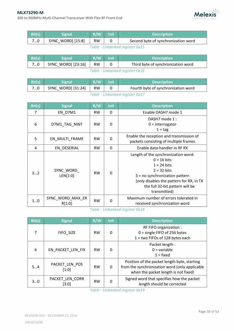
Table - Unbanked register 0x14
MLX73290-M 300 to 960MHz Multi-Channel Transceiver With Flex RF Front-End
Page 30 of 53
REVISION 010 – DECEMBER 22, 2016
3901073290
Bit(s) Signal R/W Init Description
7…0 SYNC_WORD[ [15:8] RW 0 Second byte of synchronization word
Table - Unbanked register 0x15
Bit(s) Signal R/W Init Description
7…0 SYNC_WORD[ [23:16] RW 0 Third byte of synchronization word
Table - Unbanked register 0x16
Bit(s) Signal R/W Init Description
7…0 SYNC_WORD[ [31:24] RW 0 Fourth byte of synchronization word
Table - Unbanked register 0x17
Bit(s) Signal R/W Init Description
7 EN_D7M1 RW 0 Enable DASH7 mode 1
6 D7M1_TAG_NINT RW 0 DASH7 mode 1 : 0 = interrogator
1 = tag
5 EN_MULTI_FRAME RW 0 Enable the reception and transmission of
packets consisting of multiple frames
4 EN_DESERIAL RW 0 Enable data-handler in RF RX
3…2 SYNC_WORD_
LEN[1:0] RW 0
Length of the synchronization word: 0 = 16 bits 1 = 24 bits 2 = 32 bits
3 = no synchronization pattern (only disables the pattern for RX, in TX
the full 32-bit pattern will be transmitted)
1…0 SYNC_WORD_MAX_ER
R[1:0] RW 0
Maximum number of errors tolerated in received synchronization word
Table - Unbanked register 0x18
Bit(s) Signal R/W Init Description
7 FIFO_SIZE RW 0 RF FIFO organization :
0 = single FIFO of 256 bytes 1 = two FIFOs of 128 bytes each
6 EN_PACKET_LEN_FIX RW 0 Packet length :
0 = variable 1 = fixed
5…4 PACKET_LEN_POS
[1:0] RW 0
Position of the packet length byte, starting from the synchronization word (only applicable
when the packet length is not fixed)
3…0 PACKET_LEN_CORR
[3:0] RW 0
Signed word that specifies how the packet length should be corrected
Table - Unbanked register 0x19

MLX73290-M 300 to 960MHz Multi-Channel Transceiver With Flex RF Front-End
Page 31 of 53
REVISION 010 – DECEMBER 22, 2016
3901073290
Bit(s) Signal R/W Init Description
7…0 PACKET_LEN[7:0] RW 0 Packet length in fixed packet length mode, maximum packet length for receive with
variable packet length
Table - Unbanked register 0x1A
Bit(s) Signal R/W Init Description
7…0 ADDRESS[7:0] RW 0 Address to be transmitted or checked when
address byte is enabled
Table - Unbanked register 0x1B
Bit(s) Signal R/W Init Description
7…5 CENTER_FREQ[2:0] RW 0 Lower 3 bits of the fractional division ratio of
the PLL for the center frequency
4…0 Reserved R 0 Not used, reads as 0
Table - Unbanked register 0x1C
Bit(s) Signal R/W Init Description
7…0 CENTER_FREQ[10:3] RW 0 Middle 8 bits of the fractional division ratio of
the PLL for the center frequency
Table - Unbanked register 0x1D
Bit(s) Signal R/W Init Description
7…0 CENTER_FREQ[18:11] RW 0 Upper 8 bits of the fractional division ratio of
the PLL for the center frequency
Table - Unbanked register 0x1E
Bit(s) Signal R/W Init Description
7…6 Reserved R 0 Not used, reads as 0
5…0 CENTER_FREQ[24:19] RW 0 Upper 6 bits of the center frequency,
corresponding to the integer division ratio of the PLL
Table - Unbanked register 0x1F
Bit(s) Signal R/W Init Description
7…6 Reserved R 0
5 PWRDET2_EN RW 0 Enable power detector 2
4 PWRDET1_EN RW 0 Enable power detector 1
3…2 RF_FE_EN[1:0] RW 0 RF front-end mask :
Bit 0 = Enable RF front-end 1 Bit 1 = Enable RF front-end 2
1…0 BAND_SEL[1:0] RW 0
RF frequency band selection : 0 = 299 – 331 MHz frequency range 1 = 425 – 471 MHz frequency range 2 = 607 – 615 MHz frequency range

MLX73290-M 300 to 960MHz Multi-Channel Transceiver With Flex RF Front-End
Page 32 of 53
REVISION 010 – DECEMBER 22, 2016
3901073290
3 = 864 – 956 MHz frequency range
Table - Unbanked register 0x20
Bit(s) Signal R/W Init Description
7…6 DR_LIMIT[1:0] RW 0
Limits of the data rate recovery : 0 = no data rate recovery
1 = ± 3.1% of the data rate 2 = ± 6.3% of the data rate
3 = ± 12.5% of the data rate
4…0 Reserved R 0
2…0 DR_E[2:0] RW 0 Exponent to set the data rate
Table - Unbanked register 0x21
Bit(s) Signal R/W Init Description
7…6 Reserved R 0
5…0 DR_M[5:0] RW 0 Mantissa to set the data rate
Table - Unbanked register 0x22
Bit(s) Signal R/W Init Description
7…4 MULT_EXP[3:0] RW 0 Scaling to be applied to the pulse shaping
coefficients by shifting them in the modulator, equivalent to 2MULT_EXP
3…0 MULT_MANTISSA[3:0] RW 0 Mantissa of the coefficient that multiplies the signal, equal to (16 + MULT_MANTISSA) / 16
Table - Unbanked register 0x23
Bit(s) Signal R/W Init Description
7…3 Reserved R 0 Not used, reads as 0
2…0 TX_RAMP[2:0] RW 0
TX ramp up/down duration: 0 = no ramp up/down
1 = 32 s
2 = 16 s
3 = 8 s
4 = 192 s
5 = 96 s
6 = 48 s
7 = 24 s
Table - Unbanked register 0x24
Bit(s) Signal R/W Init Description
7…0 PREAMBLE_LEN[7:0] RW 0 Length of the preamble to be transmitted
Table - Unbanked register 0x25

MLX73290-M 300 to 960MHz Multi-Channel Transceiver With Flex RF Front-End
Page 33 of 53
REVISION 010 – DECEMBER 22, 2016
3901073290
Bit(s) Signal R/W Init Description
7 IQ_CORR_EN RW 0 Enable I/Q imbalance correction
6 IQ_CORR_CAL RW 0
I/Q imbalance calibration in progress; set this bit to start I/Q imbalance calibration,
automatically cleared by hardware when calibration is finished. Clear this bit to abort
calibration. IQ_CORR_EN does not need to be set for the calibration.
5…4 RF_RSSI_DEC[1:0] RW 0
Decay rate of RF RSSI : –1.5 dB at 0 = 1x symbol rate 1 = 2x symbol rate 2 = 4x symbol rate 3 = 8x symbol rate
3…0 RF_CHANBW[3:0] RW 0
RF channel bandwidth : 0 = 600 kHz 1 = 300 kHz 2 = 200 kHz 3 = 150 kHz 4 = 120 kHz 5 = 100 kHz 6 = 75 kHz 7 = 60 kHz 8 = 50 kHz 9 = 38 kHz
10 = 30 kHz 11 = 25 kHz 12 = 19 kHz 13 = 15 kHz 14 = 13 kHz 15 = 9 kHz
Table - Unbanked register 0x26
Bit(s) Signal R/W Init Description
7 LSB_FIRST RW 0 Select the bit order :
0 = MSB first 1 = LSB first
6 BIT_INVERT RW 0 Invert the polarity of the data bits
5 EN_MANCHESTER RW 0 Enable Manchester coding of the data bits
4 EN_DATAWHITE RW 0 Enable data whitening
3 EN_PREAMBLE RW 0 Enable transmission of a preamble
2 EN_PACKET RW 0 Enable transmission and reception of packets
1 EN_CRC RW 0 Add CRC to transmitted packets, check CRC of
received packets
0 EN_ADDRESS RW 0 Add address byte to transmitted packets, check
address byte in received packets for match
Table - Unbanked register 0x27
MLX73290-M 300 to 960MHz Multi-Channel Transceiver With Flex RF Front-End
Page 34 of 53
REVISION 010 – DECEMBER 22, 2016
3901073290
Bit(s) Signal R/W Init Description
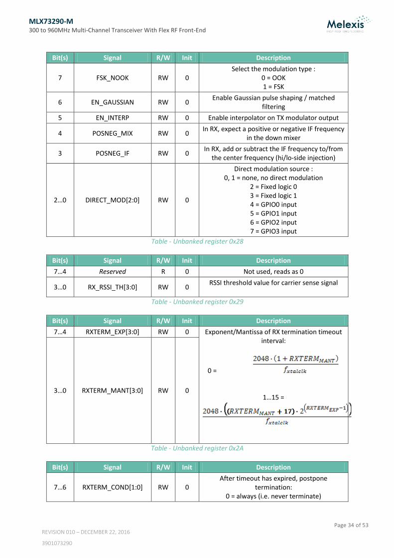
7 FSK_NOOK RW 0 Select the modulation type :
0 = OOK 1 = FSK
6 EN_GAUSSIAN RW 0 Enable Gaussian pulse shaping / matched
filtering
5 EN_INTERP RW 0 Enable interpolator on TX modulator output
4 POSNEG_MIX RW 0 In RX, expect a positive or negative IF frequency
in the down mixer
3 POSNEG_IF RW 0 In RX, add or subtract the IF frequency to/from
the center frequency (hi/lo-side injection)
2…0 DIRECT_MOD[2:0] RW 0
Direct modulation source : 0, 1 = none, no direct modulation
2 = Fixed logic 0 3 = Fixed logic 1 4 = GPIO0 input 5 = GPIO1 input 6 = GPIO2 input 7 = GPIO3 input
Table - Unbanked register 0x28
Bit(s) Signal R/W Init Description
7…4 Reserved R 0 Not used, reads as 0
3…0 RX_RSSI_TH[3:0] RW 0 RSSI threshold value for carrier sense signal
Table - Unbanked register 0x29
Bit(s) Signal R/W Init Description
7…4 RXTERM_EXP[3:0] RW 0 Exponent/Mantissa of RX termination timeout interval:
0 =
1…15 =
3…0 RXTERM_MANT[3:0] RW 0
Table - Unbanked register 0x2A
Bit(s) Signal R/W Init Description
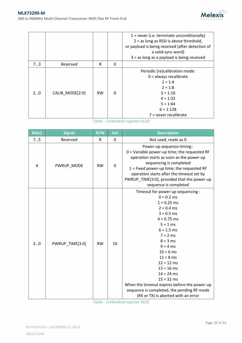
7…6 RXTERM_COND[1:0] RW 0 After timeout has expired, postpone
termination: 0 = always (i.e. never terminate)
MLX73290-M 300 to 960MHz Multi-Channel Transceiver With Flex RF Front-End
Page 35 of 53
REVISION 010 – DECEMBER 22, 2016
3901073290
1 = never (i.e. terminate unconditionally) 2 = as long as RSSI is above threshold,
or payload is being received (after detection of a valid sync word)
3 = as long as a payload is being received
7…3 Reserved R 0
2…0 CALIB_MODE[2:0] RW 0
Periodic (re)calibration mode: 0 = always recalibrate
1 = 1:4 2 = 1:8
3 = 1:16 4 = 1:32 5 = 1:64
6 = 1:128 7 = never recalibrate
Table - Unbanked register 0x2B
Bit(s) Signal R/W Init Description
7…5 Reserved R 0 Not used, reads as 0
4 PWRUP_MODE RW 0
Power-up sequence timing : 0 = Variable power-up time; the requested RF
operation starts as soon as the power-up sequencing is completed
1 = Fixed power-up time; the requested RF operation starts after the timeout set by
PWRUP_TIME[3:0], provided that the power-up sequence is completed
3…0 PWRUP_TIME[3:0] RW 10
Timeout for power-up sequencing : 0 = 0.2 ms
1 = 0.25 ms 2 = 0.4 ms 3 = 0.5 ms
4 = 0.75 ms 5 = 1 ms
6 = 1.5 ms 7 = 2 ms 8 = 3 ms 9 = 4 ms
10 = 6 ms 11 = 8 ms
12 = 12 ms 13 = 16 ms 14 = 24 ms 15 = 32 ms
When the timeout expires before the power-up sequence is completed, the pending RF mode
(RX or TX) is aborted with an error
Table - Unbanked register 0x2C
MLX73290-M 300 to 960MHz Multi-Channel Transceiver With Flex RF Front-End
Page 36 of 53
REVISION 010 – DECEMBER 22, 2016
3901073290
Bit(s) Signal R/W Init Description
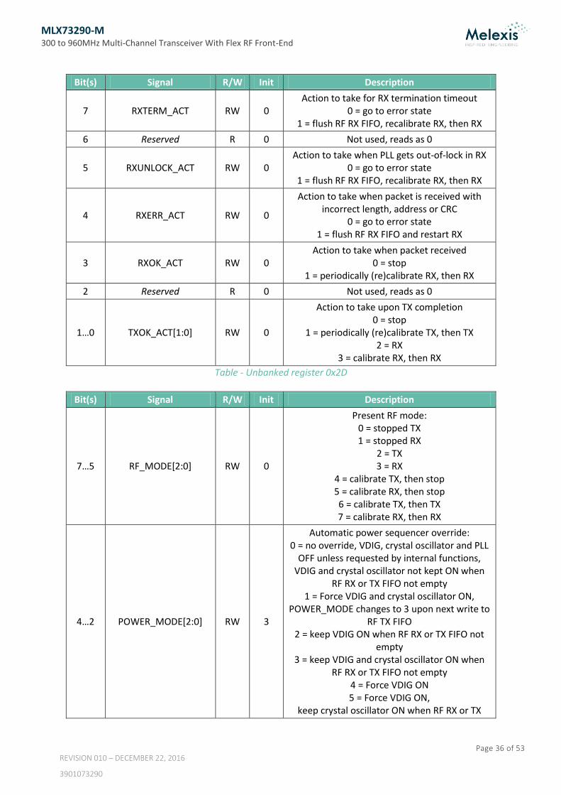
7 RXTERM_ACT RW 0 Action to take for RX termination timeout
0 = go to error state 1 = flush RF RX FIFO, recalibrate RX, then RX
6 Reserved R 0 Not used, reads as 0
5 RXUNLOCK_ACT RW 0 Action to take when PLL gets out-of-lock in RX
0 = go to error state 1 = flush RF RX FIFO, recalibrate RX, then RX
4 RXERR_ACT RW 0
Action to take when packet is received with incorrect length, address or CRC
0 = go to error state 1 = flush RF RX FIFO and restart RX
3 RXOK_ACT RW 0 Action to take when packet received
0 = stop 1 = periodically (re)calibrate RX, then RX
2 Reserved R 0 Not used, reads as 0
1…0 TXOK_ACT[1:0] RW 0
Action to take upon TX completion 0 = stop
1 = periodically (re)calibrate TX, then TX 2 = RX
3 = calibrate RX, then RX
Table - Unbanked register 0x2D
Bit(s) Signal R/W Init Description
7…5 RF_MODE[2:0] RW 0
Present RF mode: 0 = stopped TX 1 = stopped RX
2 = TX 3 = RX
4 = calibrate TX, then stop 5 = calibrate RX, then stop 6 = calibrate TX, then TX 7 = calibrate RX, then RX
4…2 POWER_MODE[2:0] RW 3
Automatic power sequencer override: 0 = no override, VDIG, crystal oscillator and PLL
OFF unless requested by internal functions, VDIG and crystal oscillator not kept ON when
RF RX or TX FIFO not empty 1 = Force VDIG and crystal oscillator ON,
POWER_MODE changes to 3 upon next write to RF TX FIFO
2 = keep VDIG ON when RF RX or TX FIFO not empty
3 = keep VDIG and crystal oscillator ON when RF RX or TX FIFO not empty
4 = Force VDIG ON 5 = Force VDIG ON,
keep crystal oscillator ON when RF RX or TX
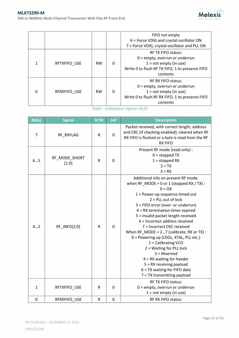
MLX73290-M 300 to 960MHz Multi-Channel Transceiver With Flex RF Front-End
Page 37 of 53
REVISION 010 – DECEMBER 22, 2016
3901073290
FIFO not empty 6 = Force VDIG and crystal oscillator ON
7 = Force VDIG, crystal oscillator and PLL ON
1 RFTXFIFO_USE RW 0
RF TX FIFO status: 0 = empty, overrun or underrun
1 = not empty (in use) Write 0 to flush RF TX FIFO, 1 to preserve FIFO
contents
0 RFRXFIFO_USE RW 0
RF RX FIFO status: 0 = empty, overrun or underrun
1 = not empty (in use) Write 0 to flush RF RX FIFO, 1 to preserve FIFO
contents
Table - Unbanked register 0x2E
Bit(s) Signal R/W Init Description
7 RF_RXFLAG R 0
Packet received, with correct length, address and CRC (if checking enabled); cleared when RF RX FIFO is flushed or a byte is read from the RF
RX FIFO
6…5 RF_MODE_SHORT
[1:0] R 0
Present RF mode (read-only) : 0 = stopped TX 1 = stopped RX
2 = TX 3 = RX
4…2 RF_INFO[2:0] R 0
Additional info on present RF mode, when RF_MODE = 0 or 1 (stopped RX / TX) :
0 = OK 1 = Power-up sequence timed out
2 = PLL out of lock 3 = FIFO error (over- or underrun) 4 = RX termination timer expired 5 = Invalid packet length received
6 = Incorrect address received 7 = Incorrect CRC received
When RF_MODE = 2…7 (calibrate, RX or TX) : 0 = Powering up (LDOs, XTAL, PLL etc.)
1 = Calibrating VCO 2 = Waiting for PLL lock
3 = Reserved 4 = RX waiting for header 5 = RX receiving payload
6 = TX waiting for FIFO data 7 = TX transmitting payload
1 RFTXFIFO_USE R 0 RF TX FIFO status:
0 = empty, overrun or underrun 1 = not empty (in use)
0 RFRXFIFO_USE R 0 RF RX FIFO status:

MLX73290-M 300 to 960MHz Multi-Channel Transceiver With Flex RF Front-End
Page 38 of 53
REVISION 010 – DECEMBER 22, 2016
3901073290
0 = empty, overrun or underrun 1 = not empty (in use)
Table - Unbanked register 0x2F (read)
Bit(s) Signal R/W Init Description
7…5 RF_MODE[2:0] W 0
Present RF mode: 0 = stopped TX 1 = stopped RX
2 = TX 3 = RX
4 = calibrate TX, then stop 5 = calibrate RX, then stop 6 = calibrate TX, then TX 7 = calibrate RX, then RX
4…2 Reserved R -
1 RFTXFIFO_USE W 0 Write 0 to flush RF TX FIFO, 1 to preserve FIFO
contents
0 RFRXFIFO_USE W 0 Write 0 to flush RF RX FIFO, 1 to preserve FIFO
contents
Table - Unbanked register 0x2F (write)
Bit(s) Signal R/W Init Description
7…0 RFTXFIFO_CNT[7:0] R 0
Number of bytes in the RF TX FIFO When the FIFO contains 256 bytes,
RFTXFIFO_CNT will be 0 but RFTXFIFO_USE will be active. When RFTXFIFO_USE is 0,
RFTXFIFO_CNT is normally 0 (FIFO empty) but can also indicate an underrun (count = 254) or
overrun (count = 255)
Table - Unbanked register 0x30
Bit(s) Signal R/W Init Description
7…0 RFRXFIFO_CNT[7:0] R 0 Number of bytes in the RF RX FIFO When the FIFO contains 256 bytes,
RFRXFIFO_CNT will be 0 but RFRXFIFO_USE will be active. When RFRXFIFO_USE is 0,
RFRXFIFO_CNT is normally 0 (FIFO empty) but can also indicate an underrun (count = 254) or
overrun (count = 255)
Table - Unbanked register 0x31
Bit(s) Signal R/W Init Description
7…0 RFRXFIFO[7:0] R - Accesses the data in the RF RX FIFO The register address is not auto-incremented
Table - Unbanked register 0x32 (read)
Bit(s) Signal R/W Init Description

MLX73290-M 300 to 960MHz Multi-Channel Transceiver With Flex RF Front-End
Page 39 of 53
REVISION 010 – DECEMBER 22, 2016
3901073290
7…0 RFTXFIFO[7:0] W - Accesses the RF TX FIFO The register address is not auto-incremented
Table - Unbanked register 0x32 (write)
Bit(s) Signal R/W Init Description
7…0 RANDOM[7:0] R 0 Random data, harvested noise of Sigma-Delta ADCs
The register address is not auto-incremented
Table - Unbanked register 0x33
10.2. Status Byte & GPIOs (0x34 to 0x3B)
Addr bit 7 bit 6 bit 5 bit 4 bit 3 bit 2 bit 1 bit 0
Status
34
35 BATTOK PLL_
LOCKED CYCLE_
SLIP RSSI_ GOOD
FEI_OK
GPIO multiplexing
36 GPIO3 GPIO2 GPIO1 GPIO0
37 GPIO3_DRV[1:0] GPIO2_DRV[1:0] GPIO1_DRV[1:0] GPIO0_DRV[1:0]
38 GPIO0_CH_SEL[6:0]
39 GPIO1_CH_SEL[6:0]
3A GPIO2_CH_SEL[6:0]
3B GPIO3_CH_SEL[6:0]
Table - Unbanked register map : Status & GPIOs
Bit(s) Signal R/W Init Description
7 BATTOK R - Started in :
0 = Battery backup mode 1 = Normal mode
6 PLL_LOCKED R - PLL is currently in-lock
5 CYCLE_SLIP RC - A PLL cycle-slip has been registered since the
last read from this register (cleared by reading this register)
4 RSSI_GOOD R - RSSI level above threshold (carrier sense)
3 FEI_OK R - Frequency error indicator stable
2…0 Reserved R 0
Table - Unbanked register 0x35
Bit(s) Signal R/W Init Description
7…4 Reserved R 0 Not used, reads as 0
3 GPIO3 R - Current level of GPIO3
2 GPIO2 R - Current level of GPIO2
1 GPIO1 R - Current level of GPIO1

MLX73290-M 300 to 960MHz Multi-Channel Transceiver With Flex RF Front-End
Page 40 of 53
REVISION 010 – DECEMBER 22, 2016
3901073290
0 GPIO0 R - Current level of GPIO0
Table - Unbanked register 0x36
Bit(s) Signal R/W Init Description
7…6 GPIO3_DRV[1:0] RW 0
Sets the driving strength of GPIO3 when used as digital output:
0 = 3 mA 1 = 6 mA 2 = 9 mA
3 = 12 mA
5…4 GPIO2_DRV[1:0] RW 0 Sets the driving strength of GPIO2 when used
as digital output
3…2 GPIO1_DRV[1:0] RW 0 Sets the driving strength of GPIO1 when used
as digital output
1…0 GPIO0_DRV[1:0] RW 0 Sets the driving strength of GPIO0 when used
as digital output
Table - Unbanked register 0x37
Bit(s) Signal R/W Init Description
7 Reserved R 0
6…0 GPIO0_CH_SEL[6:0] RW 0x12 See section 5.12
Table - Unbanked register 0x38
Bit(s) Signal R/W Init Description
7 Reserved R 0
6…0 GPIO1_CH_SEL[6:0] RW 0x13 See section 5.12
Table - Unbanked register 0x39
Bit(s) Signal R/W Init Description
7 Reserved R 0
6…0 GPIO2_CH_SEL[6:0] RW 0x34 See section 5.12
Table - Unbanked register 0x3A
Bit(s) Signal R/W Init Description
7 Reserved R 0
6…0 GPIO3_CH_SEL[6:0] RW 0x14 See section 5.12
Table - Unbanked register 0x3B
10.3. General Purpose ADC (0x3C to 0x3F)
Addr bit 7 bit 6 bit 5 bit 4 bit 3 bit 2 bit 1 bit 0
GPADC
3C ADC_REF_SEL[2:0] ADC_CH_SEL[3:0]
3D ADC_
NEWDATA
ADC_ CONTINU
ADC_CLK_SEL[1:0] ADC_START
_EOC
3E ADC_CAL[7:0]
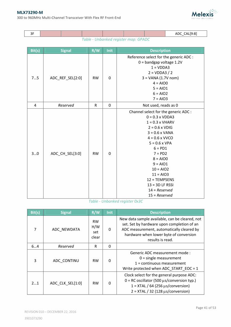
MLX73290-M 300 to 960MHz Multi-Channel Transceiver With Flex RF Front-End
Page 41 of 53
REVISION 010 – DECEMBER 22, 2016
3901073290
3F ADC_CAL[9:8]
Table - Unbanked register map: GPADC
Bit(s) Signal R/W Init Description
7…5 ADC_REF_SEL[2:0] RW 0
Reference select for the generic ADC : 0 = bandgap voltage 1.2V
1 = VDDA3 2 = VDDA3 / 2
3 = VANA (1.7V nom) 4 = AIO0 5 = AIO1 6 = AIO2 7 = AIO3
4 Reserved R 0 Not used, reads as 0
3…0 ADC_CH_SEL[3:0] RW 0
Channel select for the generic ADC : 0 = 0.3 x VDDA3 1 = 0.3 x VHARV 2 = 0.6 x VDIG 3 = 0.6 x VANA 4 = 0.6 x VVCO 5 = 0.6 x VPA
6 = PD1 7 = PD2 8 = AIO0 9 = AIO1
10 = AIO2 11 = AIO3
12 = TEMPSENS 13 = 3D LF RSSI 14 = Reserved 15 = Reserved
Table - Unbanked register 0x3C
Bit(s) Signal R/W Init Description
7 ADC_NEWDATA
RW H/W set
clear
0
New data sample available, can be cleared, not set. Set by hardware upon completion of an ADC measurement, automatically cleared by
hardware when lower byte of conversion results is read.
6…4 Reserved R 0
3 ADC_CONTINU RW 0
Generic ADC measurement mode : 0 = single measurement
1 = continuous measurement Write protected when ADC_START_EOC = 1
2…1 ADC_CLK_SEL[1:0] RW 0
Clock select for the general purpose ADC:
0 = RC oscillator (500 s/conversion typ.)
1 = XTAL / 64 (256 s/conversion)
2 = XTAL / 32 (128 s/conversion)
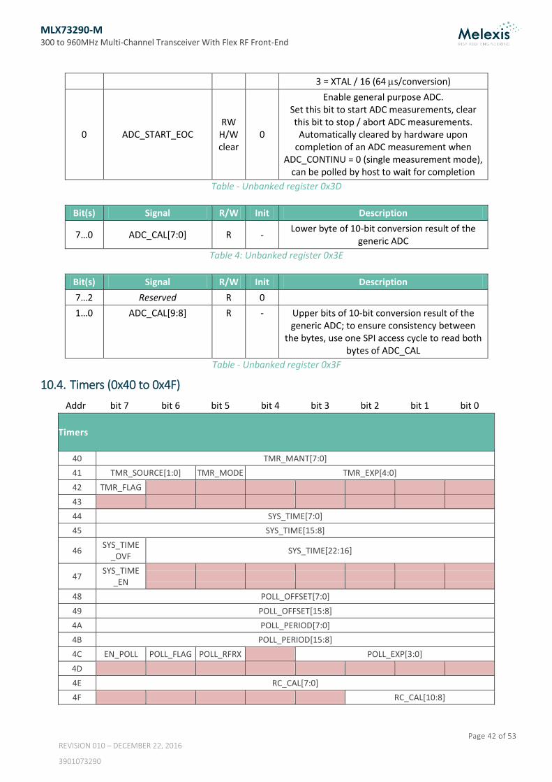
MLX73290-M 300 to 960MHz Multi-Channel Transceiver With Flex RF Front-End
Page 42 of 53
REVISION 010 – DECEMBER 22, 2016
3901073290
3 = XTAL / 16 (64 s/conversion)
0 ADC_START_EOC RW
H/W clear
0
Enable general purpose ADC. Set this bit to start ADC measurements, clear this bit to stop / abort ADC measurements.
Automatically cleared by hardware upon completion of an ADC measurement when
ADC_CONTINU = 0 (single measurement mode), can be polled by host to wait for completion
Table - Unbanked register 0x3D
Bit(s) Signal R/W Init Description
7…0 ADC_CAL[7:0] R - Lower byte of 10-bit conversion result of the
generic ADC
Table 4: Unbanked register 0x3E
Bit(s) Signal R/W Init Description
7…2 Reserved R 0
1…0 ADC_CAL[9:8] R - Upper bits of 10-bit conversion result of the generic ADC; to ensure consistency between
the bytes, use one SPI access cycle to read both bytes of ADC_CAL
Table - Unbanked register 0x3F
10.4. Timers (0x40 to 0x4F)
Addr bit 7 bit 6 bit 5 bit 4 bit 3 bit 2 bit 1 bit 0
Timers
40 TMR_MANT[7:0]
41 TMR_SOURCE[1:0] TMR_MODE TMR_EXP[4:0]
42 TMR_FLAG
43
44 SYS_TIME[7:0]
45 SYS_TIME[15:8]
46 SYS_TIME
_OVF SYS_TIME[22:16]
47 SYS_TIME
_EN
48 POLL_OFFSET[7:0]
49 POLL_OFFSET[15:8]
4A POLL_PERIOD[7:0]
4B POLL_PERIOD[15:8]
4C EN_POLL POLL_FLAG POLL_RFRX POLL_EXP[3:0]
4D
4E RC_CAL[7:0]
4F RC_CAL[10:8]

MLX73290-M 300 to 960MHz Multi-Channel Transceiver With Flex RF Front-End
Page 43 of 53
REVISION 010 – DECEMBER 22, 2016
3901073290
Table - Unbanked register map: Timers
Bit(s) Signal R/W Init Description
7…0 TMR_MANT[7:0] RW 0
8-bit period of programmable timer / clock generator; changes are glitch-free in clock
generator mode Period = (TMR_MANT+1)·2TMR_EXP clocks
Table - Unbanked register 0x40 (programmable timer)
Bit(s) Signal R/W Init Description
7…6 TMR_SOURCE[1:0] RW 2
Clock source selector for programmable timer / clock generator :
0 = OFF, timer stopped and reset 1 = 32 MHz (typ.) crystal clock 2 = 32 kHz (typ.) RC oscillator
3 = 15.6 kHz (typ.) calibrated RC clock Changes are glitch-free in clock generator mode
5 TMR_MODE RW 0
Mode of programmable timer / clock generator :
0 = Clock generator 1 = Timer
4…0 TMR_EXP[4:0] RW 0 5-bit prescaler ratio of programmable timer /
clock generator; changes are glitch-free in clock generator mode
Table - Unbanked register 0x41 (programmable timer)
Bit(s) Signal R/W Init Description
7 TMR_FLAG RW -
Output of programmable timer / clock generator
IRQ flag in timer mode, that will stop the timer and needs to be cleared by the microcontroller
6…0 Reserved R 0 Not used, reads as 0
Table - Unbanked register 0x42 (programmable timer)
Bit(s) Signal R/W Init Description
7…0 SYS_TIME[7:0] RC 0 Lower byte of 23-bit free-running system time Any write to this register will reset the entire
system time including the overflow flag
Table - Unbanked register 0x44 (system timer)
Bit(s) Signal R/W Init Description
7…0 SYS_TIME[15:8] RC 0
Middle byte of 23-bit free-running system time To ensure consistency between the bytes, use one SPI access cycle to read the lower, middle
and upper byte of the system time
Table - Unbanked register 0x45 (system timer)

MLX73290-M 300 to 960MHz Multi-Channel Transceiver With Flex RF Front-End
Page 44 of 53
REVISION 010 – DECEMBER 22, 2016
3901073290
Bit(s) Signal R/W Init Description
7 SYS_TIME_OVF RC 0 Overflow of the free-running system time, can be cleared by setting this bit to 0 through SPI
6…0 SYS_TIME[22:16] RC 0
Upper byte of 23-bit free-running system time To ensure consistency between the bytes, use one SPI access cycle to read the lower, middle
and upper byte of the system time
Table - Unbanked register 0x46 (system timer)
Bit(s) Signal R/W Init Description
7 SYS_TIME_EN RW 0 Enable free-running system time
Disabling the system time will pause the system time, but not clear it
6…0 Reserved R 0
Table - Unbanked register 0x47 (system timer)
Bit(s) Signal R/W Init Description
7…0 POLL_OFFSET[7:0] RW 0 Lower byte of 16-bit offset of RF polling timer
Table - Unbanked register 0x48 (RF polling timer)
Bit(s) Signal R/W Init Description
7…0 POLL_OFFSET[15:8] RW 0
Upper byte of 16-bit offset of RF polling timer
Offset = sec
Table - Unbanked register 0x49 (RF polling timer)
Bit(s) Signal R/W Init Description
7…0 POLL_PERIOD[7:0] RW 0 Lower byte of 16-bit period of RF polling timer
Table - Unbanked register 0x4A (RF polling timer)
Bit(s) Signal R/W Init Description
7…0 POLL_PERIOD[15:8] RW 0 Upper byte of 16-bit period of RF polling timer Period =
sec
Table - Unbanked register 0x4B (RF polling timer)
Bit(s) Signal R/W Init Description
7 EN_POLL RW 0 Enable RF polling timer
6 POLL_FLAG RW 0 IRQ flag of RF polling timer, set when timer
expires
5 POLL_RFRX RW 0 Enable RF RX polling
4 Reserved R 0
3…0 POLL_EXP[3:0] RW 0 4-bit prescaler ratio of RF polling timer
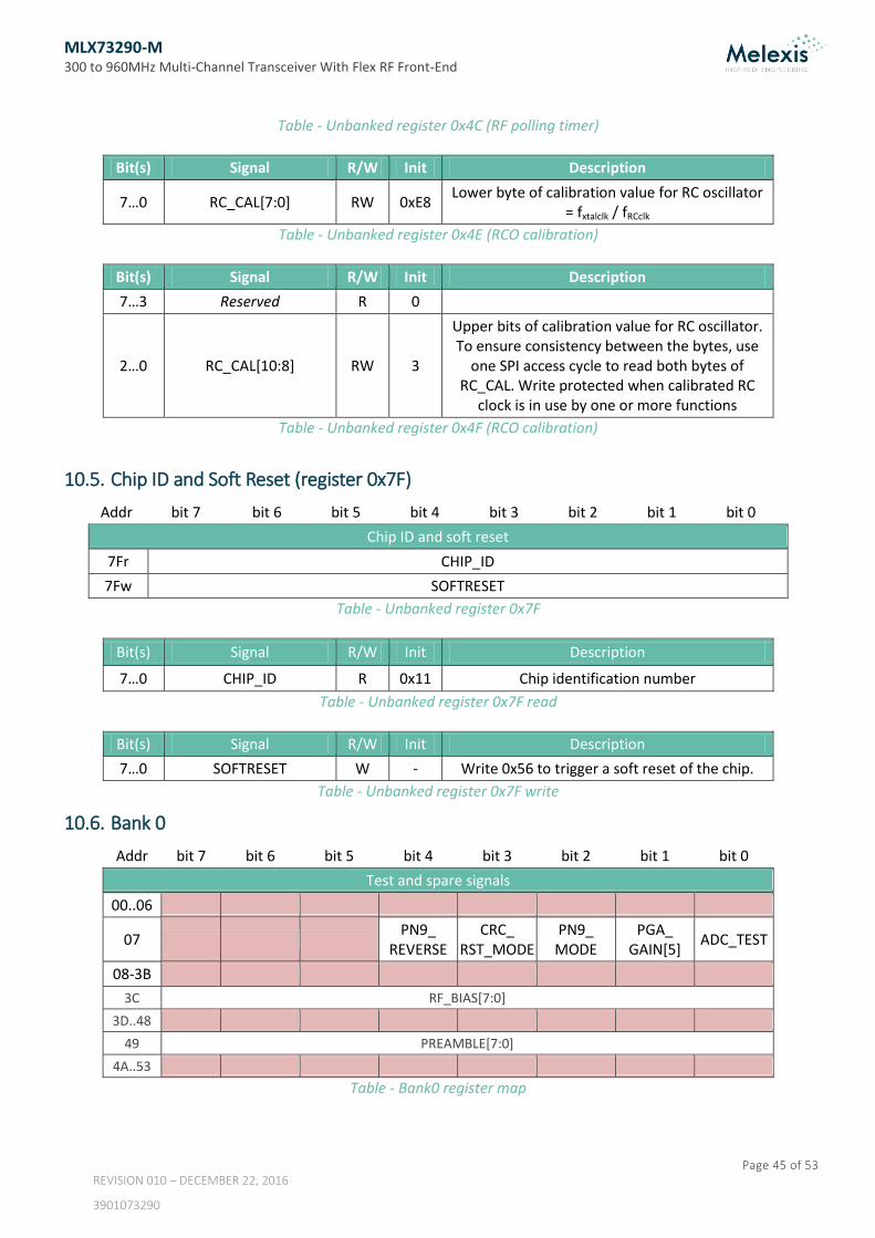
MLX73290-M 300 to 960MHz Multi-Channel Transceiver With Flex RF Front-End
Page 45 of 53
REVISION 010 – DECEMBER 22, 2016
3901073290
Table - Unbanked register 0x4C (RF polling timer)
Bit(s) Signal R/W Init Description
7…0 RC_CAL[7:0] RW 0xE8 Lower byte of calibration value for RC oscillator
= fxtalclk / fRCclk
Table - Unbanked register 0x4E (RCO calibration)
Bit(s) Signal R/W Init Description
7…3 Reserved R 0
2…0 RC_CAL[10:8] RW 3
Upper bits of calibration value for RC oscillator. To ensure consistency between the bytes, use
one SPI access cycle to read both bytes of RC_CAL. Write protected when calibrated RC
clock is in use by one or more functions
Table - Unbanked register 0x4F (RCO calibration)
10.5. Chip ID and Soft Reset (register 0x7F)
Addr bit 7 bit 6 bit 5 bit 4 bit 3 bit 2 bit 1 bit 0
Chip ID and soft reset
7Fr CHIP_ID
7Fw SOFTRESET
Table - Unbanked register 0x7F
Bit(s) Signal R/W Init Description
7…0 CHIP_ID R 0x11 Chip identification number
Table - Unbanked register 0x7F read
Bit(s) Signal R/W Init Description
7…0 SOFTRESET W - Write 0x56 to trigger a soft reset of the chip.
Table - Unbanked register 0x7F write
10.6. Bank 0
Addr bit 7 bit 6 bit 5 bit 4 bit 3 bit 2 bit 1 bit 0
Test and spare signals
00..06
07 PN9_
REVERSE CRC_
RST_MODE PN9_
MODE PGA_
GAIN[5] ADC_TEST
08-3B
3C RF_BIAS[7:0]
3D..48
49 PREAMBLE[7:0]
4A..53
Table - Bank0 register map

MLX73290-M 300 to 960MHz Multi-Channel Transceiver With Flex RF Front-End
Page 46 of 53
REVISION 010 – DECEMBER 22, 2016
3901073290
Bit(s) Signal R/W Init Description
7…5 Reserved R 0 Not used, reads as 0
4 PN9_REVERSE RW 1 Generate PN9 sequence :
0 = LSB first 1 = MSB first
3 CRC_RST_MODE RW 0 Initialize CRC to :
0 = 0x0000 1 = 0xFFFF
2 PN9_MODE RW 1 Perform PN9 sequence with reversed byte.
1..0 Reserved R 0
Table 5 - Bank0 register 0x07
Bit(s) Signal R/W Init Description
7…0 RF_BIAS[7:0] RW 0
Enable the RF RX functionality, has to be set to the following values depending on the
frequency band selected:
315MHz = 0x4C 433MHz = 0x63
868MHz and 915MHz = 0x99
Table - Bank0 register 0x3C
Bit(s) Signal R/W Init Description
7…0 PREAMBLE[7:0] RW 0x55 Preamble pattern to be repeated according to PREAMBLE_LEN[7:0] in unbanked register 0x25
Table - Bank0 register 0x49
11. Application Information
11.1. Typical Application Schematic
A possible application circuit of the MLX73290-M is shown in the below Figure. The circuit features two RF front-ends with power detectors in place. Antenna space or frequency diversity can be performed via antenna 1 and antenna 2. An energy harvester (like a solar cell) could be used for supplying the transceiver IC at pin VHARV. The MCU controls the RF transceiver via its SPI bus and it connects to the GPIO bus.

MLX73290-M 300 to 960MHz Multi-Channel Transceiver With Flex RF Front-End
Page 47 of 53
REVISION 010 – DECEMBER 22, 2016
3901073290
4
4
NC
XTALN
VSSA
SCK
SDI
SDO
GPIO0
GPIO1
CS
GP
IO2
GP
IO3
VS
SD
VD
IG
VM
AIN
VD
DD
3
VH
AR
V
VPA
VSSA
PD1
RF1P
VSSA
NC
RF1N
VD
DA
3
VS
SA
PD
2
RF
2P
RF
2N
VS
SA
VA
NA
VD
DA
3
XTALP
MLX73290-M
30MHz - 34MHz
balun 2
Battery
to Battery
2.1V - 3.6V
XTAL
SPI BUS
EXT SUPPLY
GPIO BUS
matching network
C0
C1
C3 C4
C5
C6 C7
C9_2C8_2
C11_2
C10_2
C12_2
L0_2
L1_2
L2_2
L3_2
C2
balun 1
RF antenna 1
L0_1 L1_1
L2_1
L3_1
C9_1C8_1
C10_1
C11_1
C12_1
matching
network
RF antenna 2
VHARHV
MCU
solar
cell
Figure 17: Typical application schematic
11.1.1. TX/RX Combining Network
The RF ports of the MLX73290-M have been designed in order to achieve optimum performance in both TX and RX mode as well as for different RF power levels and at various frequency bands. For this purpose two inductors are used per single-ended RF port. Pin VPA connects to the four inductors of the TX/RX combining network. In TX mode, this pin is internally switched to positive supply, and so it supplies the output transistor of the cascoded power amplifier (PA). In RX mode, pin VPA is internally connected to ground, and the transistor is now part of the LNA that behaves as a common-gate amplifier. As a result the RF port impedance in RX mode matches the impedance in TX mode, yielding optimum performance in both modes. An alternative TX/RX combining network with less inductors can be used (and will be presented later).
11.1.2. Balun
A balanced-to-unbalanced transformer (balun) is used to convert the differential input/output of the MLX73290-M to a single-ended signal from/to the RF antenna. Off-the-shelf baluns are available on the market, depending on the wanted frequency range, the actual implementation will vary. Some SAW filters can also fulfil a balun functionality, which may be an interesting solution if it is necessary to filter out harmonics to comply with regulatory requirements. The easiest solution is to realize a lumped balun with discrete external components and integrated it within the RF matching network. A simple balun topology is illustrated below.

MLX73290-M 300 to 960MHz Multi-Channel Transceiver With Flex RF Front-End
Page 48 of 53
REVISION 010 – DECEMBER 22, 2016
3901073290
Figure 18: Balun made with discrete components
11.1.3. External Power Switch Usage
In the special case where the microcontroller does not have a low power standby mode (as would be for example the case with some dedicated secure code), the overall power consumption can be reduced by using the integrated polling mechanism and using an external power switch, e.g. a power MOSFET, as illustrated in Figure 19.
Figure 19: MCU supplied through an external power switch
In that specific case, one of the GPIO signals can be used to control an external power switch which is useful to cut down the residual power consumption of the microcontroller. Note that the chip select wire of the SPI interface has been defined active high specifically for this application. This avoids having the MLX73290-M “selected” when the microcontroller power is down.
Differential
signal
CB0
“Single”
signal
LB0
CB1
LB1
Generic µCSDI
SDO
VD
IG
VM
AIN
VD
DD
3
GP
IO3 GPIO1
CS
SCK
VS
SD
MLX73290
GP
IO2
GPIO0
SP
I b
us
VDD
Power switch

MLX73290-M 300 to 960MHz Multi-Channel Transceiver With Flex RF Front-End
Page 49 of 53
REVISION 010 – DECEMBER 22, 2016
3901073290
12. Performance Plots
12.1. Spectrum Plots
Figure 20: FSK (black) and GFSK (blue) spectrum at 250kbps, ±50kHz deviation
MLX73290-M 300 to 960MHz Multi-Channel Transceiver With Flex RF Front-End
Page 50 of 53
REVISION 010 – DECEMBER 22, 2016
3901073290
12.2. Eye Diagram
Figure 21: 250kbps GMSK transmit signal eye diagram at 868MHz
12.3. Phase Noise
434MHz
868MHz
Figure 22: 434MHz and 868MHz phase noise plots

MLX73290-M 300 to 960MHz Multi-Channel Transceiver With Flex RF Front-End
Page 51 of 53
REVISION 010 – DECEMBER 22, 2016
3901073290
13. Manufacturability of Melexis Products with Different Soldering Processes
Our products are classified and qualified regarding soldering technology, solderability and moisture sensitivity level according to following test methods: Reflow Soldering SMD’s (Surface Mount Devices) IPC/JEDEC J-STD-020
Moisture/Reflow Sensitivity Classification for Nonhermetic Solid State Surface Mount Devices (classification reflow profiles according to table 5-2)
EIA/JEDEC JESD22-A113 Preconditioning of Nonhermetic Surface Mount Devices Prior to Reliability Testing (reflow profiles according to table 2)
Wave Soldering SMD’s (Surface Mount Devices) and THD’s (Through Hole Devices) EN60749-20
Resistance of plastic- encapsulated SMD’s to combined effect of moisture and soldering heat EIA/JEDEC JESD22-B106 and EN60749-15
Resistance to soldering temperature for through-hole mounted devices Iron Soldering THD’s (Through Hole Devices) EN60749-15
Resistance to soldering temperature for through-hole mounted devices Solderability SMD’s (Surface Mount Devices) and THD’s (Through Hole Devices) EIA/JEDEC JESD22-B102 and EN60749-21
Solderability For all soldering technologies deviating from above mentioned standard conditions (regarding peak temperature, temperature gradient, temperature profile etc) additional classification and qualification tests have to be agreed upon with Melexis. The application of Wave Soldering for SMD’s is allowed only after consulting Melexis regarding assurance of adhesive strength between device and board. Melexis is contributing to global environmental conservation by promoting lead free solutions. For more information on qualifications of RoHS compliant products (RoHS = European directive on the Restriction Of the use of certain Hazardous Substances) please visit the quality page on our website: http://www.melexis.com/quality.aspx
14. ESD Precautions
Electronic semiconductor products are sensitive to Electro Static Discharge (ESD). Always observe Electro Static Discharge control procedures whenever handling semiconductor products.

MLX73290-M 300 to 960MHz Multi-Channel Transceiver With Flex RF Front-End
Page 52 of 53
REVISION 010 – DECEMBER 22, 2016
3901073290
15. Package Information
The device MLX73290-M is RoHS compliant.
Figure 23: 32L QFN 5x5 Quad
all Dimension in mm
D E D2 E2 A A1 A3 L e b
min 4.75 4.75 3.00 3.00 0.80 0 0.20
0.3 0.50
0.18
max 5.25 5.25 3.25 3.25 1.00 0.05 0.5 0.30
all Dimension in inch
min 0.187 0.187 0.118 0.118 0.0315 0 0.0079
0.0118 0.0197
0.0071
max 0.207 0.207 0.128 0.128 0.0393 0.002 0.0197 0.0118
Table - 32L QFN5x5
MLX73290-M 300 to 960MHz Multi-Channel Transceiver With Flex RF Front-End
Page 53 of 53
REVISION 010 – DECEMBER 22, 2016
3901073290
16. Contact
For the latest version of this document, go to our website at www.melexis.com. For additional information, please contact our Direct Sales team and get help for your specific needs:
Europe, Africa Telephone: +32 13 67 04 95
Email : [email protected]
Americas Telephone: +1 603 223 2362
Email : [email protected]
Asia Email : [email protected]
17. Disclaimer The information furnished by Melexis herein (“Information”) is believed to be correct and accurate. Melexis disclaims (i) any and all liability in connection with or arising out of the furnishing, performance or use of the technical data or use of the product(s) as described herein (“Product”) (ii) any and all liability, including without limitation, special, consequential or incidental damages, and (iii) any and all warranties, express, statutory, implied, or by description, includ ing warranties of fitness for particular purpose, non-infringement and merchantability. No obligation or liability shall arise or flow out of Melexis’ rendering of technical or other services. The Information is provided "as is” and Melexis reserves the right to change the Information at any time and without notice. Therefore, before placing orders and/or prior to designing the Product into a system, users or any third party should obtain the latest version of the relevant information to verify that the information being relied upon is current. Users or any third party must further determine the suitability of the Product for its application, including the level of re liability required and determine whether it is fit for a particular purpose. The Information is proprietary and/or confidential information of Melexis and the use thereof or anything described by the In formation does not grant, explicitly or implicitly, to any party any patent rights, licenses, or any other intellectual property rights. This document as well as the Product(s) may be subject to export control regulations. Please be aware that export might require a prior authorization from competent authorities. The Product(s) are intended for use in normal commercial applications. Unless otherwise agreed upon in writing, the Product(s) are not designed, authorized or warranted to be suitable in applications requiring extended temperature range and/or unusual environmental requirements. High reliability applications, such as medical life-support or life-sustaining equipment are specifically not recommended by Melexis. The Product(s) may not be used for the following applications subject to export control regulations: the development, product ion, processing, operation, maintenance, storage, recognition or proliferation of 1) chemical, biological or nuclear weapons, or for the development, production, maintenance or storage of missiles for such weapons: 2) civil firearms, including spare parts or ammunition for such arms; 3) defense related products, or other material for military use or for law enforcement; 4) any applications that, alone or in combination with other goods, substances or organisms could cause serious harm to persons or goods and that can be used as a means of violence in an armed conflict or any similar violent situation. The Products sold by Melexis are subject to the terms and conditions as specified in the Terms of Sale, which can be found at https://www.melexis.com/en/legal/terms-and-conditions. This document supersedes and replaces all prior information regarding the Product(s) and/or previous versions of this document. Melexis NV © - No part of this document may be reproduced without the prior written consent of Melexis. (2016) ISO/TS 16949 and ISO14001 Certified