Minimum and Maximum Modes For 8086 Microprocessor and... · These signals enable an IO interface to...
21
Minimum and Maximum Modes For 8086 Microprocessor
Transcript of Minimum and Maximum Modes For 8086 Microprocessor and... · These signals enable an IO interface to...

Minimum and Maximum Modes For 8086 Microprocessor

ROAD MAP
• General Bus Operation
• Minimum Mode configuration In 8086
• Maximum Mode Configuration In 8086
2

3
General Bus Operation
The 8086 has a combined address and data bus commonly referredas a time multiplexed address and data bus.The main reason behind multiplexing address and data over thesame pins is the maximum utilization of processor pins and itfacilitates the use of 40 pin standard DIP package.
The bus can be demultiplexed using a few latches andtransreceivers, when ever required.
Basically, all the processor bus cycles consist of at least four clockcycles. These are referred to as T1, T2, T3, T4. The address istransmitted by the processor during T1. It is present on the busonly for one cycle.

The negative edge of this ALE pulse is used to separate theaddress and the data or status information. In maximummode, the status lines S0, S1 and S2 are used to indicatethe type of operation.
Status bits S3 to S7 are multiplexed with higher orderaddress bits and the BHE signal.
Address is valid during T1 while status bits S3 to S7 arevalid during T2 through T4.
4

5
General Bus Cycle For 8086

6
Minimum Mode 8086 System The microprocessor 8086 is operated in minimum mode by
strapping its MN/MX pin to logic 1.
In this mode, all the control signals are given out by themicroprocessor chip itself. There is a single microprocessor inthe minimum mode system.
The remaining components in the system are latches,transreceivers, clock generator, memory and I/O devices.
Latches are generally buffered output D-type flip-flops like74LS373 or 8282. They are used for separating the valid addressfrom the multiplexed address/data signals and are controlled bythe ALE signal generated by 8086.

7
Minimum Mode Configuration For 8086

8
Transreceivers are the bidirectional buffers and some times they arecalled as data amplifiers. They are required to separate the valid datafrom the time multiplexed address/data signals. They are controlled bytwo signals namely, DEN and DT/R.
The DEN signal indicates the direction of data, i.e. from or to theprocessor.
The system contains memory for the monitor and users programstorage. Usually, EPROM are used for monitor storage, while RAM forusers program storage. A system may contain I/O devices.
The opcode fetch and read cycles are similar. Hence the timingdiagram can be categorized in two parts, the first is the timing diagramfor read cycle and the second is the timing diagram for write cycle.
The read cycle begins in T1 with the assertion of address latch enable(ALE) signal and also M / IO signal. During the negative going edge ofthis signal, the valid address is latched on the local bus.

9
The BHE and A0 signals address low, high or both bytes. FromT1 to T4 , the M/IO signal indicates a memory or I/Ooperation.
At T2, the address is removed from the local bus and is sent tothe output. The bus is then tristated. The read (RD) controlsignal is also activated in T2.
The read (RD) signal causes the address device to enable its databus drivers. After RD goes low, the valid data is available on thedata bus.
The addressed device will drive the READY line high. When theprocessor returns the read signal to high level, the addresseddevice will again tristate its bus drivers.

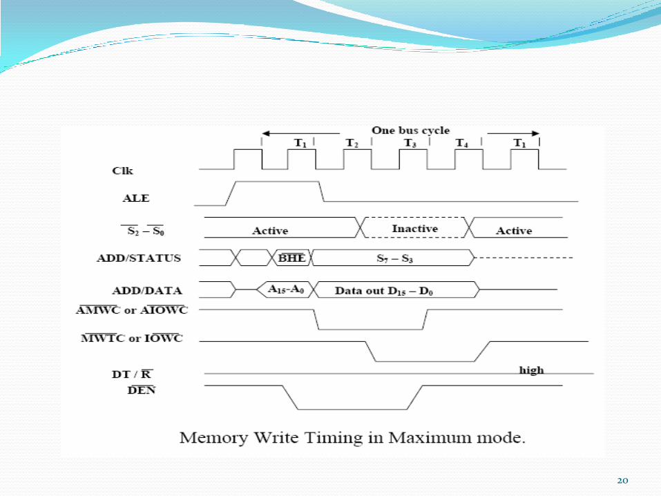
A write cycle also begins with the assertion of ALE and theemission of the address.
The M/IO signal is again asserted to indicate a memory or I/Ooperation. In T2, after sending the address in T1, the processorsends the data to be written to the addressed location.
The data remains on the bus until middle of T4 state. The WRbecomes active at the beginning of T2 (unlike RD is somewhatdelayed in T2 to provide time for floating).
The BHE and A0 signals are used to select the proper byte orbytes of memory or I/O word to be read or write.
The M/IO, RD and WR signals indicate the type of data transferas specified in table below.
10

11

12
Hold Response sequence:
The HOLD pin is checked at leading edge of each clock pulse.
If it is received active by the processor before T4 of the previouscycle or during T1 state of the current cycle, the CPU activatesHLDA in the next clock cycle and for succeeding bus cycles, thebus will be given to another requesting master.
The control of the bus is not regained by the processor until therequesting master does not drop the HOLD pin low.
When the request is dropped by the requesting master, theHLDA is dropped by the processor at the trailing edge of thenext clock.
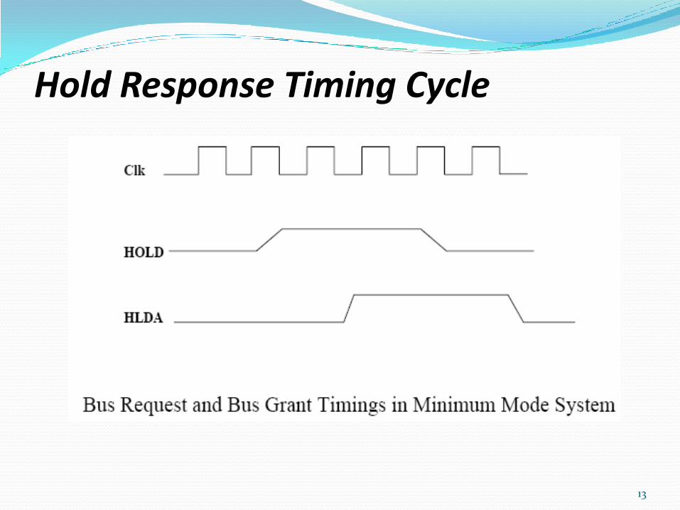
13
Hold Response Timing Cycle

14
Maximum Mode 8086 System
In the maximum mode, the 8086 is operated by strapping theMN/MX pin to ground.
In this mode, the processor derives the status signal S2, S1, S0.Another chip called bus controller derives the control signal usingthis status information .
In the maximum mode, there may be more than onemicroprocessor in the system configuration. The components inthe system are same as in the minimum mode system.
The basic function of the bus controller chip IC8288, is to derivecontrol signals like RD and WR ( for memory and I/O devices),DEN, DT/R, ALE etc. using the information by the processor on thestatus lines.

15
The bus controller chip has input lines S2, S1, S0 and CLK.These inputs to 8288 are driven by CPU.
It derives the outputs ALE, DEN, DT/R, MRDC, MWTC,AMWC, IORC, IOWC and AIOWC. The AEN, IOB and CENpins are specially useful for multiprocessor systems.
AEN and IOB are generally grounded. CEN pin is usually tied to+5V. The significance of the MCE/PDEN output depends uponthe status of the IOB pin.
INTA pin used to issue two interrupt acknowledge pulses to theinterrupt controller or to an interrupting device.

IORC, IOWC are I/O read command and I/O write commandsignals respectively . These signals enable an IO interface to reador write the data from or to the address port.
The MRDC, MWTC are memory read command and memorywrite command signals respectively and may be used asmemory read or write signals.
All these command signals instructs the memory to accept orsend data from or to the bus.
Here the only difference between in timing diagram betweenminimum mode and maximum mode is the status signals usedand the available control and advanced command signals.
16

17
Maximum Mode Configuration For 8086

18
R0, S1, S2 are set at the beginning of bus cycle.8288 bus controller willoutput a pulse as on the ALE and apply a required signal to its DT / Rpin during T1.
In T2, 8288 will set DEN=1 thus enabling transceivers, and for an inputit will activate MRDC or IORC. These signals are activated until T4.
For an output, the AMWC or AIOWC is activated from T2 to T4 andMWTC or IOWC is activated from T3 to T4.
The status bit S0 to S2 remains active until T3 and become passiveduring T3 and T4.
If reader input is not activated before T3, wait state will be insertedbetween T3 and T4.

19
20

THANKS!
For more Notes Follow http://www.edutechlearners.com