Miniaturized Microwave Devices and Antennas for …Miniaturized Microwave Devices and Antennas for...
169
Miniaturized Microwave Devices and Antennas for Wearable, Implantable and Wireless Applications Muhammad Ali Babar Abbasi Department of Electrical Engineering Frederick University, Nicosia, Cyprus A thesis submitted for the degree of PhD – Electrical Engineering 2017 arXiv:1806.00379v1 [physics.app-ph] 1 Jun 2018
Transcript of Miniaturized Microwave Devices and Antennas for …Miniaturized Microwave Devices and Antennas for...
Miniaturized Microwave Devices and
Antennas for Wearable, Implantable
and Wireless Applications
Muhammad Ali Babar Abbasi
Department of Electrical Engineering
Frederick University, Nicosia, Cyprus
A thesis submitted for the degree of
PhD – Electrical Engineering
2017
arX
iv:1
806.
0037
9v1
[ph
ysic
s.ap
p-ph
] 1
Jun
201
8

Dedicated to my parents.

Acknowledgements
Praise be to Allah úÍAªK ð é
K AjJ., the Most Gracious, the Most Mer-
ciful, for blessing me with the strength to complete this work. I pray
that the growth I achieved would be used in his cause. I am infinitely
grateful to my parents for passing down the values and constant en-
couragement throughout my educational career. I thank the Frederick
University for giving me the opportunity to pursue my doctoral stud-
ies. I am also thankful to the Erasmus Mundus INTACT doctoral
level scholarship program for funding my research. I am thankful to
the School of Electrical Engineering and Computer Sciences, National
University of Sciences and Technology (NUST), Islamabad, Pakistan
in grooming my research aptitude. Specifically, I am grateful to Dr.
Munir Ahmed Tarar for advising my thesis. I am thankful to COM-
SATS Institute of Information and Technology, Islamabad, Pakistan
for providing me strong undergraduate education and to Dr. Syed
Muzahir Abbas for his guidance.
I would like to extend my profound gratitude to my mentor and prin-
cipal advisor Dr. Symeon Nikolaou for his constant guidance and
encouragement that I received from him. He trusted in me, always
held me to a high standard, and encouraged me to work hard. In
addition to being my advisor, he is an amazing person and I have
been thoroughly enriched working with him. It has been an honor for
me to work under his supervision. I am also thankful to Dr. Marco
A. Antoniades for his active participation in my research endeavors
throughout my tenure at Frederick University. He always encouraged
and supported me. He extended his help by allowing me to be a part
of his research laboratory at the University of Cyprus (UCY). I would

like to thank Dr. Photos Vrionides for his constant support and kind
words. I would like to thank Professor Antonije R. Djordjevic and Dr.
Marija M. Nikolic for their help and guidance while my scientific mis-
sion in the University of Belgrade, Serbia. Also, thanks to Tim and
Harish from Cambridge University for contributing in public CUED
Latex material.
I would like to thank my friends who made my stay in Cyprus the
most memorable, always supported me and encouraged me, tolerated
my sarcasm, and accepted me with my workaholic nature. Thanks to
Waqar (the guide), Salman (the information), Naveed (doctor sab),
Taqua (the kindness), Christina (the humbleness), Mostafa (the inspi-
ration), Rafay (the discipline), (sweet) Abdul, Agne (the amazing),
Yousaf (the curious), Haroon (the help), Zunaib (the calm), Aqeela
(the taste) and Zainab (the fun). I could always count on the support
and encouragement from Badar bhai, Haroon bhai and family, also
from Saleem, Rizwan, Ilyas, Hamza, Sahar, Ambreen and Hassan,
even remotely. I also enjoyed the company of Dr. Hassaan, Maria
Api and kids, Sir Zeeshan, Sir Ajmal, Dr. Adnan, Dr. Umer, Ms.
Rania, Birendra (late), Diogo, Daniela, Kinga, Andreas(s), Hanne,
Constantinos, Ouan, Mohamed, Kata, Simran, George, Marilena(s),
Angelena, Krisztina, Veronica, Dora, Chloe, Mainul Haque, James,
Krish, Ahmed, Winnie, Talha, Parash, Melanie and Sergio. The time
spent with my colleagues, working as a team, deep discussions, long
walks, adventures, travelling within Cyrus and abroad, road trips, and
most of all the sleepless nights working in the lab and time spent in
“PhD House” will always be a valuable part of my memory.
Abstract
This thesis presents a number of microwave devices and antennas that
maintain high operational efficiency and are compact in size at the
same time. One goal of this thesis is to address several miniaturization
challenges of antennas and microwave components by using the theo-
retical principles of metamaterials, metasurfaces coupling resonators
and stacked radiators, in combination with the elementary antenna
and transmission line theory. While innovating novel solutions, stan-
dards and specifications of next generation wireless and bio-medical
applications were considered to ensure advancement in the respec-
tive scientific fields. A compact reconfigurable phase-shifter based on
negative-refractive-index transmission-line (NRI-TL) materialist unit
cells is presented. The corresponding work focuses on implementa-
tion of two inter-switchable NRI-TL metamaterial unit cells collocated
within the same board area in a reconfigurable manner. In addition
to phase shifter, a practical implementation of a miniaturized mi-
crowave crossover using NRI-TL metamaterials is demonstrated. The
metamaterial theory has signify that by loading a conventional trans-
mission line with lumped LC elements, a large phase shift per-unit-
length can be achieved. Using this feature of NRI-TL metamaterials,
the miniaturization of a crossover has been achieved by replacing the
conventional microstrip transmission lines in a three-section branch-
line coupler crossover with NRI-TL metamaterials lines, representing
a compact NRI-TL crossover with an area 47 times smaller than the
area of the conventional counterpart. By moving from 1D metamateri-
als to 2D metasurfaces, an array of Electromagnetic Band Gap (EBG)
structures is introduce. The corresponding study discussed the use of
an EBG array structure as a director for efficient radiation of a wear-
able antenna. A planar monopole printed on a partially grounded
substrate is first loaded with a M×N EBG structure to achieve a
maximum directivity along the z -axis when the antenna is placed in
the x-y plane. A successful attempt of miniaturizing such structure
to a 2×1 element array excited by a monopole to form an efficient
antenna is presented. The reflection phase of a single EBG unit cell
has been studied and exploited towards efficient radiation of planar
monopole. The shape of the EBG unit cell and the gap between the
ground and the EBG layer are adjusted so that the antenna operates
at 2.45 GHz. The proposed antenna retained its impedance matching
when placed directly upon a living human subject with an impedance
bandwidth of 5%, while it exhibits a measured gain of 6.88 dBi. A
novel equivalent array model is presented to qualitatively explain the
radiation mechanism of the antenna. In the next study, a fork shaped
wearable sensor antenna is designed by utilizing the available ground
space of the EBG backed monopole. The antenna is designed to ef-
ficiently radiate towards the human body while keeping the detuning
and impedance mismatching affects to a minimum, which are reported
to be inevitable due to body loading. For this study, a high resolu-
tion numerical human body phantom was used and Finite Difference
Time-domain (FDTD) solver was used as a simulation environment.
Challenges and possible solutions for through-body communication
has been investigated. Next, a fully parametrized solution for an im-
plantable antenna is proposed using metallic coated stacked substrate
layers. The intended solution makes it possible to use the proposed
antenna structure as an implant at several different areas of the hu-
man body with potentially distinct electrical properties with conse-
quently different detuning effect. Particle swarm algorithm has been
implemented to optimize the antenna performance while operating
inside distinct human tissue surroundings. Within dead tissue (quasi
in-vivo) operation of the implantable antenna, on-body operation of
the wearable sensor antenna, and an efficient communication of EBG

backed monopole with an off-body transceiver depicts a practical so-
lution for body-centric wireless communication system. The entire
study answered several research questions of applied electromagnetic
in the field of bio-medicine. Next, miniaturization and implementa-
tion of a UWB antenna along with an analytical model to predict
the resonance is presented. Lastly, several miniaturized rectifiers de-
signed specifically for efficient wireless power transfer are proposed,
experimentally verified, and discussed.

Contents
Contents vii
List of Figures xi
Nomenclature xviii
1 Introduction 1
1.1 Motivation . . . . . . . . . . . . . . . . . . . . . . . . . . . . . . . 1
1.2 Objectives . . . . . . . . . . . . . . . . . . . . . . . . . . . . . . . 2
1.3 Organization of the Dissertation . . . . . . . . . . . . . . . . . . 2
2 Metamaterial Based Electrically Small Microwave Devices 4
2.1 Introduction to Metamaterials . . . . . . . . . . . . . . . . . . . . 5
2.1.1 Electromagnetic wave propagation in metamaterials . . . . 6
2.1.2 Metamaterial Applications . . . . . . . . . . . . . . . . . . 9
2.2 Reconfigurable NRI-TL Metamaterial Phase Shifter . . . . . . . . 10
2.2.1 Design Process . . . . . . . . . . . . . . . . . . . . . . . . 12
2.2.2 Optimization Algorithm . . . . . . . . . . . . . . . . . . . 15
2.2.3 Realization . . . . . . . . . . . . . . . . . . . . . . . . . . 18
2.2.4 Results and Discussion . . . . . . . . . . . . . . . . . . . . 21
vii

CONTENTS
2.3 A Compact NRI-TL Metamaterial Microstrip Crossover . . . . . 23
2.3.1 Implementation . . . . . . . . . . . . . . . . . . . . . . . . 24
2.3.2 Fabrication and Measurements . . . . . . . . . . . . . . . . 27
2.4 Chapter Conclusions . . . . . . . . . . . . . . . . . . . . . . . . . 28
3 Metasurface Based Miniaturized Wearable Antenna 30
3.1 Introduction to Metasurfaces . . . . . . . . . . . . . . . . . . . . . 31
3.1.1 Possible application of Metamaterial and Metasurfaces . . 32
3.2 2×1 EBG-backed Planar Monopole Antenna Design . . . . . . . . 34
3.2.1 Antenna Configuration and EBG Structure Selection . . . 36
3.2.2 Antenna Miniaturization . . . . . . . . . . . . . . . . . . 39
3.2.3 Parametric analysis . . . . . . . . . . . . . . . . . . . . . 41
3.2.4 Radiation performance and mechanism . . . . . . . . . . . 43
3.2.5 Experimental Results . . . . . . . . . . . . . . . . . . . . 49
3.3 Analysis of Antenna for Wearable Applications . . . . . . . . . . 50
3.3.1 Effects of Structural Deformation . . . . . . . . . . . . . . 50
3.3.2 Human body loading . . . . . . . . . . . . . . . . . . . . . 54
3.3.3 Specific Absorption Rate (SAR) analysis . . . . . . . . . . 57
3.4 Chapter Conclusions . . . . . . . . . . . . . . . . . . . . . . . . . 59
4 Electrically Small Implantable Antenna 61
4.1 Design Challenges . . . . . . . . . . . . . . . . . . . . . . . . . . . 62
4.2 Multi-layered Implantable Antenna . . . . . . . . . . . . . . . . . 64
4.3 Numerical Phantom Selection for Implant Study . . . . . . . . . . 68
4.3.1 Simulation Setup . . . . . . . . . . . . . . . . . . . . . . . 69
4.3.2 Results and Discussion . . . . . . . . . . . . . . . . . . . . 71
viii

CONTENTS
4.4 Practical Realization . . . . . . . . . . . . . . . . . . . . . . . . . 73
4.4.1 Measurements within Tissue . . . . . . . . . . . . . . . . . 74
4.5 Chapter Contributions . . . . . . . . . . . . . . . . . . . . . . . . 75
5 Through- and across-body communication 77
5.1 Introduction . . . . . . . . . . . . . . . . . . . . . . . . . . . . . . 78
5.1.1 Wearable Sensor Antenna for Through-body communication 78
5.1.2 Wearable Sensor Node Architecture . . . . . . . . . . . . . 81
5.1.3 Simulation Test-bench . . . . . . . . . . . . . . . . . . . . 82
5.1.4 Results and Discussion . . . . . . . . . . . . . . . . . . . . 84
5.2 Across-Body Communication . . . . . . . . . . . . . . . . . . . . 84
5.2.1 Simulation Setup . . . . . . . . . . . . . . . . . . . . . . . 85
5.2.2 Results and Discussion . . . . . . . . . . . . . . . . . . . . 86
6 Miniaturized Ultra Wideband Antenna 88
6.1 Introduction on UWB Antennass . . . . . . . . . . . . . . . . . . 89
6.1.1 Electrically Small UWB Antenna Designs . . . . . . . . . 90
6.1.2 Miniaturization Procedure . . . . . . . . . . . . . . . . . . 93
6.1.3 Radiation Performance . . . . . . . . . . . . . . . . . . . . 97
6.2 Miniaturized Cactus-shaped Antenna . . . . . . . . . . . . . . . . 98
6.2.1 Geometrical Configuration . . . . . . . . . . . . . . . . . . 100
6.3 Principle of Operation . . . . . . . . . . . . . . . . . . . . . . . . 100
6.3.1 Measurement Accuracy Impediment . . . . . . . . . . . . . 109
6.4 Radiation Performance . . . . . . . . . . . . . . . . . . . . . . . . 109
6.5 Chapter Conclusions . . . . . . . . . . . . . . . . . . . . . . . . . 111
ix
CONTENTS
A Efficient Rectifiers for Wireless Power Transfer 114
A.1 Introduction and Background . . . . . . . . . . . . . . . . . . . . 114
A.2 Rectifier Design . . . . . . . . . . . . . . . . . . . . . . . . . . . . 116
A.2.1 2.45 GHz Rectifier . . . . . . . . . . . . . . . . . . . . . . 116
A.2.2 5.6 GHz Rectifier . . . . . . . . . . . . . . . . . . . . . . . 120
A.2.3 1.6 GHz Rectifier . . . . . . . . . . . . . . . . . . . . . . . 122
B List of Publications 125
References 129
x
List of Figures
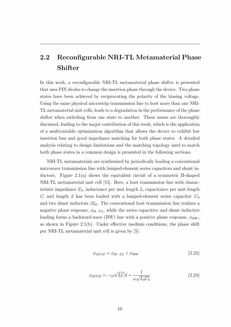
2.1 Fig.1 (a) NRI-TL metamaterial Π unit cell, (b) phase response of a
metamaterial line as a composite response of the transmission line
(TL) and backward-wave (BW) line responses, and metamaterial
line architecture for (c) phase State A, and (d) phase State B (dD
represent extra length of transmission line outside the unit cells). 12
2.2 Simulated responses for magnitude of S-parameters (left), and phase
of S21 (right) of the two-state NRI-TL metamaterial lines of Fig-
ure 2.1 (c) and (d), compared to the same length conventional
transmission line. . . . . . . . . . . . . . . . . . . . . . . . . . . 13
2.3 Simulated responses for magnitude of S-parameters (left), and phase
of S21 (right) of the NRI-TL metamaterial line as the value of the
shunt loading inductor L0 is varied from 8.0 nH in State A with
a phase of φMTM A = −15 to 1.5 nH in State B with a phase
of φMTM B = +60. The length of the unit cell size, d, and the
loading capacitance C0 remain the same for φH−TL = −70, f0 =
1 GHz, and C0 = 3.2 pF. . . . . . . . . . . . . . . . . . . . . . . . 13
2.4 Layout configuration of the two-state reconfigurable NRI-TL meta-
material phase shifter. c© 2017 IEEE. . . . . . . . . . . . . . . . . 14
2.5 Schematic of the reconfigurable NRI-TL phase shifter in Keysight –
Advanced Design System (ADS). Realistic S-parameter models of
the lumped LC components from Murata and Coilcraft were used,
together with S-parameter models from Skyworks for the OFF and
ON states of the PIN diodes. c© 2017 IEEE. . . . . . . . . . . . . 16
xi

LIST OF FIGURES
2.6 (a) Fabricated prototype of the proposed reconfigurable NRI-TL
phase shifter, (b) Zoomed-in view of the central unit cell. c© 2017
IEEE. . . . . . . . . . . . . . . . . . . . . . . . . . . . . . . . . . 18
2.7 (a) Simulated and measured responses of the reconfigurable NRI-
TL metamaterial phase shifter. (a) |S11|, (b) |S21|, (c) Phase of
S21, and (d) group delay. . . . . . . . . . . . . . . . . . . . . . . 20
2.8 Normalized surface current distribution at 1 GHz on the conduc-
tors of the NRI-TL metamaterial phase shifter in State A (left),
and State B (right). . . . . . . . . . . . . . . . . . . . . . . . . . . 21
2.9 Measured phase difference between the two states. . . . . . . . . 21
2.10 Footprint comparison between a microwave crossover using con-
ventional transmission lines and a compact NRI-TL metamaterial
microwave crossover. . . . . . . . . . . . . . . . . . . . . . . . . . 24
2.11 Two-stage NRI-TL metamaterial line formed by cascading two Π
unit cells for the implementation of each branch of the crossover. . 24
2.12 Full-wave EM simulation prototype of the three-section NRI-TL
metamaterial crossover. . . . . . . . . . . . . . . . . . . . . . . . . 26
2.13 Fabricated prototype of the compact NRI-TL metamaterial mi-
crowave crossover. (a) The device, (b) zoomed-in view of the sol-
dered lumped-element components. c© 2018 Wiley Periodicals, Inc. 28
2.14 Simulated and measured S-parameter responses for the compact
NRI-TL metamaterial microwave crossover. c© 2018 Wiley Peri-
odicals, Inc. . . . . . . . . . . . . . . . . . . . . . . . . . . . . . . 28
3.1 (a) Configuration of the 2×1 EBG-backed planar monopole an-
tenna with full ground (b) Top view of the monopole and finite
sized EBG layer. Antenna is fabricated on semi flexible Rogers
RT/duroid 5880 substrate with εr = 2.2 and tanδ = 0.0009. c©2016 IEEE. . . . . . . . . . . . . . . . . . . . . . . . . . . . . . . 37
xii
LIST OF FIGURES
3.2 (a) Configuration of a single unit cell consisting of the EBG element
with metallic backing under plane wave excitation. (b) Reflection
phase of an infinite array of the EBG unit cells. (d) Configura-
tion of a 21 array of EBG cells under plane wave excitation (d)
Reflection phase of the 21 array of EBG cells . . . . . . . . . . . . 38
3.3 Miniaturization of antenna (a) Return loss response of the steps
with percentage size reduction (b) Reflection coefficient when the
antenna is optimized in the 2.45 GHz ISM band. . . . . . . . . . . 40
3.4 Comparison of 2×1-EBG-backed monopole measured S11 with sim-
ulated S11 using finite element method (FEM) and simulated using
finite difference time domain method (FDTD). . . . . . . . . . . . 42
3.5 Parametric study of: (a) monopole length M1, (b) gap between
EBG and ground plane d2 (c) gap between RF ground and first
EBG cell g1 and (d) gap between EBG cells g2 all in mm. . . . . 43
3.6 (a) Simulated and measured y-z plane (left) and x-z plane (right)
normalized radiation patterns of the 2×1 EBG-backed monopole
antenna at 2.45 GHz. (b) Simulated and measured peak gain of
the 2×1 EBG-backed monopole . . . . . . . . . . . . . . . . . . . 44
3.7 (a) Electric field distribution on EBG surface depicting three mag-
netic current sources at 2.45 GHz (b) Equivalent eight-element
array model consisting of two electric current sources and six mag-
netic current sources, (c) Simulated electric field on the EBG layer
along the x -axis, which is used to model the magnitude of the
magnetic current sources, (d) Simulated electric field pattern of a
∼λ/4 magnetic current source. . . . . . . . . . . . . . . . . . . . . 46
3.8 Electric field patterns comparison between of 2×1 EBG-backed
monopole antenna and the eight-element array model along the
y-z plane (left) and along the x-z plane (right). . . . . . . . . . . 47
xiii
LIST OF FIGURES
3.9 Photographs of the fabricated antenna (a) on the planar monopole
side (front side) (b) on the 2×1 EBG plane side (back side) (c)
assembled integrated antenna connected to a VNA (d) Radiation
pattern measurement setup in an anechoic chamber and (e) an-
tenna supported by low-loss Styrofoam over a rotating platform
connected to an SMA connector and a balun in the anechoic cham-
ber. c© 2016 IEEE. . . . . . . . . . . . . . . . . . . . . . . . . . . 50
3.10 (a) Structurally deformed assembled 2×1 EBG-backed monopole
antenna with different values of the curvature radius, ranging from
Rx = 15 mm to 40 mm along the x -axis and from Ry = 50 mm to
80 mm along the y-axis (b) Photograph of deformed antenna. c©2016 IEEE. . . . . . . . . . . . . . . . . . . . . . . . . . . . . . . 52
3.11 (a) Simulated and measured reflection coefficient. (b) Radiation
patterns of the antenna in the y-z (left) plane and x-z plane (right)
for all deformation cases in the x -axis. . . . . . . . . . . . . . . . 52
3.12 (a) Simulated and measured reflection coefficient. (b) Radiation
patterns of the antenna in the y-z plane (left) and x-z plane (right)
for all deformation cases in the y-axis. . . . . . . . . . . . . . . . 53
3.13 Measured reflection coefficient of the assembled 2×1 EBG-backed
monopole antenna placed on different parts of the human body,
and a photograph of the antenna placed on the arm. c© 2016 IEEE. 55
3.14 2×1 EBG-backed monopole antenna placed on the (a) arm, (b)
chest and (c) leg of a realistic human body numerical phantom
to evaluate the radiation characteristics presented in terms of (d)
radiation patterns at 2.45 GHz along the y-z axis (left), along the
x-z axis (right). (e) Antenna gain and efficiency. c© 2016 IEEE. . 56
3.15 Single-layer phantom for SAR computation and 2×1 EBG-backed
monopole mounted on top of it. . . . . . . . . . . . . . . . . . . . 57
xiv
LIST OF FIGURES
3.16 SAR evaluation comparison for the 2×1 EBG-backed monopole
with extensions in the ground plane (a) along x-z evaluation plane
(b) along y-z evaluation plane [all the plots are averaged to the
maximum value of 0.5 W/kg]. c© 2016 IEEE. . . . . . . . . . . . 58
4.1 The geometry of proposed Implantable antenna. with lsub =
15mm, hsub = 0.635mm, wsub = 18mm, hcoat = 17µm, l =
13.8mm and w = 16.56mm. c© 2015 PIERS . . . . . . . . . . . . 64
4.2 Detuning of antenna when placed in 23x23x5 mm3 human skin
phantom and optimization using particle swarm algorithm at (a)
MICS band and (b) ISM band . . . . . . . . . . . . . . . . . . . . 67
4.3 Geometry of implantable antenna operating at MICS band. c©2015 PIERS. . . . . . . . . . . . . . . . . . . . . . . . . . . . . . . 69
4.4 Implanting antenna in (a) realistic human phantom i-e Case1 (b)
complex layered phantom i-e Case2 and (c) simple layered phantom
i-e Case3. c© 2015 PIERS . . . . . . . . . . . . . . . . . . . . . . 70
4.5 Return loss comparison of implantable antenna for all three cases. 72
4.6 S21 comparison for implantable antenna (left), comparison of FDTD
mesh cell count (Top right), comparison of detuning in MHz (mid-
dle right) and comparison of error observed in S-parameter for all
three cases. . . . . . . . . . . . . . . . . . . . . . . . . . . . . . . 72
4.7 Fabricated prototype with implantable antenna (a) fabricated lay-
ers after milling and cutting by milling machine (b) microscopic
photograph of middle layer showing soldered vias (c) photograph
of final implantable antenna prototype. c© 2018 IEEE. . . . . . . 73
4.8 Measurement setup of minced pork meat implant to test the per-
formance of implantable antenna. c© 2018 IEEE. . . . . . . . . . 75
4.9 Comparison between simulated and measured results for the an-
tenna prepared for minced pork meat implant. . . . . . . . . . . . 76
xv
LIST OF FIGURES
5.1 (a) Schematic of a wearable sensor antenna when L = 70, W = 38,
wa1 = 2.05, wa2 = 10.25, wa3 = 7.33, wa4 = 8.34, la1 = 22.60, la2 =
10.50, la3 = la4 = 32.89 (all parameters are in mm) (b) Normalized
E -field distribution. . . . . . . . . . . . . . . . . . . . . . . . . . 79
5.2 (a) Simulated S21 when antenna is placed on chest and moved away
from the body. (b) 2D gain plot. . . . . . . . . . . . . . . . . . . 80
5.3 (a) System level block diagram of implantable to off-body transceiver
communication via wearable node (b) Wearable device architecture
representing the operational principle when two antennas radiate
in the opposite directions. . . . . . . . . . . . . . . . . . . . . . . 82
5.4 (a) Simulation setup for wearable to implantable antenna com-
munication and normalized E -field distribution. (b) S-parameter
response when port 1 is connected to the implantable antenna and
port 2 is connected to the wearable sensor antenna. . . . . . . . . 83
5.5 (a) Simulation setup for across-body communication (b) Cross-
sectional view of the torso region at the antenna level showing the
transmitter and receiver element positions. . . . . . . . . . . . . . 86
5.6 Simulated S21 versus analytical S21 when the transmitted antenna
stays on its position while the receiver antenna is moved along the
torso from position 1 to 9. . . . . . . . . . . . . . . . . . . . . . . 86
5.7 Simulated creepy wave illustration by normalized E -field magni-
tude plot. . . . . . . . . . . . . . . . . . . . . . . . . . . . . . . . 87
6.1 Fabricated (a) CPW-fed slot antenna, (b) cactus antenna, and (c)
miniaturized cactus antenna. c© 2016 IJAP. . . . . . . . . . . . . 91
6.2 Surface current (J) distributions on CPW-fed slot antenna at (a)
5 GHz (b) 9 GHz, cactus antenna at (c) 5 GHz (d) 9 GHz and
miniaturized cactus antenna at (e) 5 GHz and (f) 9 GHz. . . . . 94
6.3 Return loss of Miniaturization process . . . . . . . . . . . . . . . 95
6.4 Return loss with S2 variation . . . . . . . . . . . . . . . . . . . . 95
xvi
LIST OF FIGURES
6.5 Return loss with L2 variation . . . . . . . . . . . . . . . . . . . . 96
6.6 Return loss with Gw variation . . . . . . . . . . . . . . . . . . . . 96
6.7 Simulated and measured gain comparison for (a) CPW -fed slot
antenna (b) Cactus antenna (c) Miniaturization cactus antenna
and (d) Comparison of measured gain for all three antennas . . . 98
6.8 Measured and simulated return loss. Red dotted line shows the
calculated resonance frequency using proposed equation. c© 2016
IEEE. . . . . . . . . . . . . . . . . . . . . . . . . . . . . . . . . . 101
6.9 Modified versions of the cactus-shaped monopole operating at se-
lected UWB sub-bands when L1 =L3 =0, L2 =12 (top left), L1 =6.5,
L2 =L3 =0 (top right), L1 =L2 =L3 =0 (bottom left) and L1 =0,
L2 =11.5, L3 =3.5 (bottom right) when all values in mm. c© 2016
IEEE. . . . . . . . . . . . . . . . . . . . . . . . . . . . . . . . . . 103
6.10 Surface current distribution on cactus-shaped radiator at 4.20 GHz
(left), 5.90 GHz (center) and 7.80 GHz (right). . . . . . . . . . . 104
6.11 Parametric study for the design parameters effect on the return
loss. left monopole effect (top left) middle monopole effect (top
right) right monopole effect (bottom left) effect of ground plane
(bottom right). In each plot other than the varied parameter the
other parameters have same values. c© 2016 IEEE. . . . . . . . . 104
6.12 Verification of equation 6.7. . . . . . . . . . . . . . . . . . . . . . 107
6.13 Predicted fL from literature = 1.56 GHz and the simulated fL =
1.79 GHz. . . . . . . . . . . . . . . . . . . . . . . . . . . . . . . . 108
6.14 The first resonance occurs because the central planar radiating
monopole at 4.2 GHz (shown in E -field plot) with inherently
wideband characteristics along with the harmonics at the higher
frequencies. . . . . . . . . . . . . . . . . . . . . . . . . . . . . . . 109
6.15 Sensitivity of antennas return loss when SMA connector slides
along the transmission line (a) The antenna size compared with
the size of attached SMA connector. Return loss when (b) SMA
connector slides along y-axis (c) SMA connector slide along x -axis. 110
xvii

LIST OF FIGURES
A.1 Rectifier and voltage doubler architecture (bottom left) and ADS
circuit schematic of the rectifier. . . . . . . . . . . . . . . . . . . . 117
A.2 Rectifier at 2.45 GHz . . . . . . . . . . . . . . . . . . . . . . . . . 118
A.3 Comparison between simulated and measured (a) |S11| vs frequency
and (b) Efficiency vs Pin at 2.45 GHz. . . . . . . . . . . . . . . . 119
A.4 Rectifier at 5.6 GHz . . . . . . . . . . . . . . . . . . . . . . . . . 121
A.5 Comparison between simulated and measured (a) |S11| vs frequency
and (b) Efficiency vs Pin at 5.6 GHz. . . . . . . . . . . . . . . . . 122
A.6 Rectifier at 1.6 GHz . . . . . . . . . . . . . . . . . . . . . . . . . 123
A.7 Comparison between simulated and measured (a) |S11| vs frequency
and (b) Efficiency vs Pin at 1.6 GHz. . . . . . . . . . . . . . . . . 123
xviii
Chapter 1
Introduction
1.1 Motivation
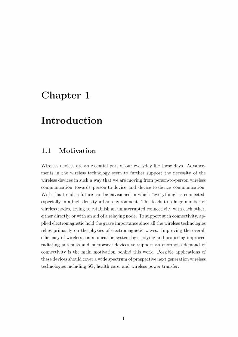
Wireless devices are an essential part of our everyday life these days. Advance-
ments in the wireless technology seem to further support the necessity of the
wireless devices in such a way that we are moving from person-to-person wireless
communication towards person-to-device and device-to-device communication.
With this trend, a future can be envisioned in which “everything” is connected,
especially in a high density urban environment. This leads to a huge number of
wireless nodes, trying to establish an uninterrupted connectivity with each other,
either directly, or with an aid of a relaying node. To support such connectivity, ap-
plied electromagnetic hold the grave importance since all the wireless technologies
relies primarily on the physics of electromagnetic waves. Improving the overall
efficiency of wireless communication system by studying and proposing improved
radiating antennas and microwave devices to support an enormous demand of
connectivity is the main motivation behind this work. Possible applications of
these devices should cover a wide spectrum of prospective next generation wireless
technologies including 5G, health care, and wireless power transfer.
1
1.2 Objectives
The major objectives of this work are: (1) designing, miniaturization and real-
ization of microwave devices/transmission lines; (2) the design of compact high
gain wearable antenna; (3) to develop an efficient implantable antenna; (4) to
develop a wearable sensor node for the communication with off-body transceiver
and an implantable antenna; (5) the development of techniques to reduce the de-
coupling and impedance miss-matching of a wearable antenna; (6) to miniaturize
the UWB antenna and (7) to design compact rectifier for low power input.
1.3 Organization of the Dissertation
As stated before, in this thesis, a number of compact microwave devices and an-
tennas are discussed and compared to current state-of-the-art. In second chapter,
elementary theory of metamaterials and metasurfaces is introduced. A compact
reconfigurable phase shifter solution inspired by NRI-TL metamaterial unit cell
is discussed. Same theory is implemented to miniaturize the size of a branch-line
coupler microwave crossover. In third chapter, a planar monopole backed with a
2×1 array of Electromagnetic Band Gap (EBG) structures is introduced, oper-
ating as a wearable antenna. In detail discussion on miniaturization procedure
along with the use of an EBG array structure as a director for efficient resonance
of a printed monopole antenna is presented. A novel radiation mechanism model
to quantify the antenna’s power patterns has been explained. Antenna has fur-
ther been tested for human body loading and structural deformation. Chapter
4 discusses an electrically small implantable antenna designed using stacked mi-
crostrip layer technology. The antenna performance has been tested in simplistic
and high resolution numerical phantom and practical implementation has been
verified by measurements. In Chapter 5, wearable sensor antenna is introduce to
study the challenges of body centric wireless communication. Through-body com-
munication has been verified between wearable sensor antenna and an implantable
antenna. Chapter 6 presents miniaturization techniques for UWB antenna and
analytical model to predict the antenna resonances using proposed geometry. Fi-
2

nally, a number of rectifiers for efficient wireless power transfer are presented and
discussed at the end of the thesis in Appendix A. The list of publications that
are either already in press or in the process of review are enlisted in Appendix B.
3
Chapter 2
Metamaterial Based Electrically
Small Microwave Devices
This chapter presents an introduction and miniaturization applications of negative-
refractive-index transmission-line (NRI-TL) metamaterial. A compact reconfig-
urable phase-shifter based on NRI-TL metamaterial unit cells is presented and
discussed. Two inter-switchable NRI-TL metamaterial unit cells are collocated
on the same board area, and can be reconfigured based on the biasing polarity of
embedded PIN diodes to provide two discrete phase states. The PIN diodes are
located on the shunt branches of the metamaterial line in order to reduce losses
in the direct signal path. Design limitations in terms of return loss and insertion
loss are discussed in relation to the two phase states. A proof-of-concept module
is designed for the phase advance of 55.5 and 128.5 in two reconfigurable states
of the module when the insertion loss for the two states is −1.43 dB and −0.89
dB respectively. Simulation and measurements are compared to test the validity
of designed phase shifter. In the end a practical implementation of a miniaturized
microwave crossover using NRI-TL metamaterials is presented.
4
2.1 Introduction to Metamaterials
The Metamaterials can be generally defined as a class of an artificial material, or
a wave propagation media, exhibiting extraordinary electromagnetic properties
that cannot be found in natural ones [1]. The name is based on a Greek letter
µετα (meta) that means “after” or “beyond” It means that the these material
do not follow the natural principles and can be terms as “µετα” physical in
nature. Metamaterials has a number of exciting applications that has drawn the
attention from the scientific community of multiple disciplines. One interesting
fact about Metamaterials is that it draw the physics and engineering community
close together based on their superior priorities shocking for the physicists, while
incredible for the engineers. There is nothing new in metamaterial theory in
terms of fundamental science and the whole theory can be understood based on
the classical electromagnetic theory. The theoretical concept of the existence of
backward-waves based on the signs of permittivity was first developed in 1904 [2]
and since then, the artificially arranged complex materials have been the subject
to scientific advancement since then.
A key feature of these artificial materials is the negative refraction. When an
Electromagnetic wave passes through these materials, the electric vector ~E, the
magnetic vector ~H and the wave vector ~k do not follow the “right hand rule” for
the electromagnetic wave propagation. In other words, the wave propagation is in
–~k direction. Due to this property, occasionally “left handed materials (LHM)”
is the title given to these materials in literature. In other literature, the property
of the materials is not focused, but the wave propagation is, so the name given is
“backward-wave materials”, which is also the term used in this thesis. The two
parameters used to characterize the electric and magnetic properties of materials
are the permittivity (ε) and the permeability (µ), when electromagnetic fields are
studied to interact the material. The measure of the changes in the medium to
absorb the electric energy is described as (ε) and it relates to the terms ~E known
as electric field strength and ~D, known as electric displacement as a result of~E. The term “relative dielectric constant” or (εr) used normally in literature is
actually the ratio of permittivity of the material to that of free space. Where the
free space permittivity denoted by (ε0) is 8.85× 10⁻¹²F/m. On the other hand,
5

the Permeability is a constant of proportionality that exists between magnetic
induction and magnetic field intensity while the free space permeability is denoted
by µ0 and is approximately 4π × 10−7H/m. It has been discussed previously
that the for the normal materials, the wave propagation’s electric and magnetic
properties are defined by the permittivity and permeability of the material. Both
these terms are positive in nature. However, for the Metamaterials, both these
terms tend to be negative, while the electromagnetic wave propagation is still
possible because the product of these terms still gives a positive. The constitutive
material parameters in terms of refractive index can be written as:
η = ±√εrµr (2.1)
So the squared η is not affected by the signs of the εr and µr.
2.1.1 Electromagnetic wave propagation in metamaterials
Let us see the Maxwell’s equation reduced to a wave equation and the general
equation of a plane wave is:
~E = ~E0e−j~kr (2.2)
~H = ~H0e−j~kr (2.3)
Where ~E0 and ~H0 are the vectors in the direction of propagation of the wave~k while ~r is the position vector for the observation point. The expressions can be
written as:
~k = kxx+ kyy + kz z (2.4)
k =√k2x + k2y + k2z (2.5)
6

~r = x.x+ y.y + z.z (2.6)
We can solve the Maxwell’s equations by transforming the system into second
order partial differential equation. Writing the equations in time harmonic form
yields:
∇× ~E = −jω ~B (2.7)
∇× ~H = jω ~D + ~J (2.8)
We also know that:
∇ · ~B = ∇ · µ ~H = 0 (2.9)
∇ · ~D = ∇ · ε ~E = ρv (2.10)
Equations 2.9 and 2.10 can be rewritten in the form:
∇× ~E = −jωµ ~H (2.11)
∇× ~H = jωε ~E + ~J (2.12)
In the medium having free charges that allow the current to flow ( ~J = σ ~E),
re-writing the Ampere’s Law will give:
∇× ~H = jωε ~E + σ ~E = jω[ε+σ
jω] ~E (2.13)
Where the term [ε+ σjω
], written as [ε− j σω
] in the phaser domain shows that
the effective complex permittivity can be represented by the a lumped expression
7

of the conductivity and the permittivity. So this expression can be represented
as:
εeff = [ε− j σω
] = ε0[εr − jσ
ωε0] = ε0εref (2.14)
And the equation 2.13 becomes:
∇× ~H = jωεeff ~E (2.15)
While the εeff is complex. For the field vectors, we know that:
~E ⊥ ~H ⊥ ~k (2.16)
So,~E = η ~H × ~k (2.17)
~H =1
η~k × ~E (2.18)
For the plane waves with expressions ~E = ~E0e−j~kr+jωt and ~H = ~H0e
−j~kr+jωt,
the equations 2.11 and 2.15 will eventually reduce to:
~k × ~E =
ωµ ~H, if µ > 0
−ω|µ| ~H, if µ < 0(2.19)
~k × ~H =
−ωε ~E, if µ > 0
ω|ε| ~E, if µ < 0(2.20)
Note that in case of both aforementioned cases i-e backward-wave and forward
wave propagation, the time averaged flux of energy is determined by:
~S =1
2~E × ~H∗ (2.21)
8
Where ~S shows the actual propagation of energy. For the case of metama-
terial, the backward-wave has ~S and ~K in reverse directions. In the proceeding
discussions in the thesis chapters, it will be shown that the most extraordinary
electromagnetic and transmission line based properties of metamaterial revolves
around this backward-wave propagation.
2.1.2 Metamaterial Applications
Artificial material engineering has enabled the design and development of com-
pact, cost-effective and high-performance solutions at microwave, terahertz and
optical frequencies. The electromagnetic behavior of metamaterial structures is
modified intentionally by adjusting either their electrical or geometrical proper-
ties to formulate non-linear materials, semiconductor structures, liquid crystals,
microfluids and so on [3]. Within the same framework, the increasing demand
for tunable microwave systems has further advanced research towards reconfig-
urability within metamaterials. At microwave frequencies, recent developments
in negative-refractive-index transmission line (NRI-TL) metamaterials [4, 5] have
enabled the design and realization of electrically small reconfigurable metamate-
rial lines. The reconfigurability is achieved by loading a host transmission line
with lumped capacitors and inductors. The practical use of such NRI-TL meta-
materials still poses a number of technological and theoretical challenges in terms
of operational bandwidth, losses, realization complexity, tuning speed and toler-
ance sensitivity. Over and above the aforementioned challenges, the inclusion
of the tuning mechanism (biasing lines and control mechanism etc.) must not
affect the desired electromagnetic behavior of the reconfigurable system. Some
prominent techniques to achieve reconfigurability include microfluidic channels
[6], CMOS-based active inductors [7], BST thick-film substrates [8], GaAs [9, 10]
and Schottky varactor diodes [11], ferroelectric varactors [12], MEMS capacitors
[13], and metal-insulator-metal MIM capacitors [14].
9
2.2 Reconfigurable NRI-TL Metamaterial Phase
Shifter
In this work, a reconfigurable NRI-TL metamaterial phase shifter is presented
that uses PIN diodes to change the insertion phase through the device. Two phase
states have been achieved by reciprocating the polarity of the biasing voltage.
Using the same physical microstrip transmission line to host more than one NRI-
TL metamaterial unit cells, leads to a degradation in the performance of the phase
shifter when switching from one state to another. These issues are thoroughly
discussed, leading to the major contribution of this work, which is the application
of a multivariable optimization algorithm that allows the device to exhibit low
insertion loss and good impedance matching for both phase states. A detailed
analysis relating to design limitations and the matching topology used to match
both phase states in a common design is presented in the following sections.
NRI-TL metamaterials are synthesized by periodically loading a conventional
microwave transmission line with lumped-element series capacitors and shunt in-
ductors. Figure 2.1(a) shows the equivalent circuit of a symmetric Π-shaped
NRI-TL metamaterial unit cell [15]. Here, a host transmission line with charac-
teristic impedance Z 0, inductance per unit length L, capacitance per unit length
C, and length d has been loaded with a lumped-element series capacitor C 0
and two shunt inductors 2L0. The conventional host transmission line realizes a
negative phase response, φH−TL, while the series capacitive and shunt inductive
loading forms a backward-wave (BW) line with a positive phase response, φBW ,
as shown in Figure 2.1(b). Under effective medium conditions, the phase shift
per NRI-TL metamaterial unit cell is given by [5]:
φMTM = φH−TL + φBW (2.22)
φMTM = −ω√LCd+
1
ω√L0C0
(2.23)
10
This is valid under the impedance matching condition below, which stipulates
that both the lines must have the same characteristic impedance.
Z0 =
√L
C=
√L0
C0
(2.24)
In this work, a microstrip transmission line with an impedance of Z 0 = 50
Ω and a fixed length of d = 35 mm is used to host two collocated and reconfig-
urable NRI-TL metamaterial phase-shifting lines that realize two discrete phase
states, State A and State B, given by φMTM A and φMTM B, respectively. The
architecture of the two individual NRI-TL metamaterial lines is shown in Figure
2.22(c) and (d). Both lines have the same series components, and differ only in
the locations and values of the shunt loading inductors, L0A and L0B.By switching
between the two inductor values, a fixed phase change can be effected, according
to (1b). A change in the value of L0 without changing C 0, however, will lead
to a mismatch along the line, since the impedance matching condition of (2.24)
will no longer apply. This is mitigated by the fact that the two metamaterial
unit cells used in Figure 2.1(c) and (d) also differ in size, given by dA and dB
respectively, providing an additional degree of freedom that is used to provide
good impedance matching in both states.
Using 2.22 and 2.23 and the design procedure outlined in [15], p. 17 with
φH−TL = −70 at a design frequency of f0 = 1 GHz, the loading element values
required to achieve a phase of φMTM A = −15 in State A are C 0 = 3.2 pF, and L0
= 8.0 nH, while to achieve a phase of φMTM B = +60 in State B the values are
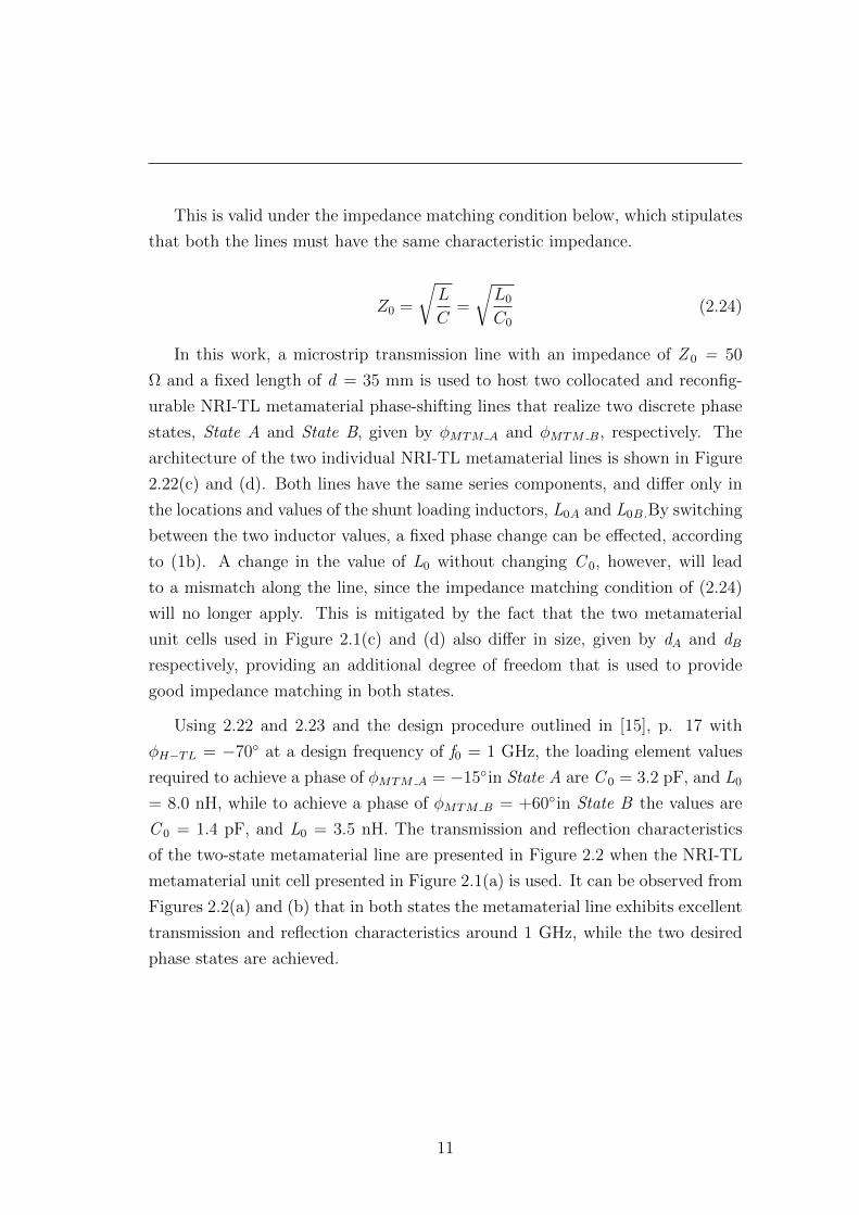
C 0 = 1.4 pF, and L0 = 3.5 nH. The transmission and reflection characteristics
of the two-state metamaterial line are presented in Figure 2.2 when the NRI-TL
metamaterial unit cell presented in Figure 2.1(a) is used. It can be observed from
Figures 2.2(a) and (b) that in both states the metamaterial line exhibits excellent
transmission and reflection characteristics around 1 GHz, while the two desired
phase states are achieved.
11
Z0 Z0
C0
2L0 2L0
d
(a)
ϕMTM= ϕH-TL+ϕBW
f
ϕ(°)
(b)
Z0 Z0 Z0 Z0
C0
2L0A 2L0A
dA/2 dA/2 dD/2
dA
d
Z0 Z0
dD/2 dC/2 dC/2
(c)
Z0 Z0 Z0 Z0
C0
2L0B 2L0B
dA/2 dA/2 dD/2
dB
d
Z0 Z0
dD/2 dC/2 dC/2
(d)
Figure 2.1: Fig.1 (a) NRI-TL metamaterial Π unit cell, (b) phase response ofa metamaterial line as a composite response of the transmission line (TL) andbackward-wave (BW) line responses, and metamaterial line architecture for (c)phase State A, and (d) phase State B (dD represent extra length of transmissionline outside the unit cells).
2.2.1 Design Process
Combining two NRI-TL metamaterial unit lines representing two distinct phase
states poses two major challenges. Firstly, when the same transmission line is
used to host two NRI-TL unit cells with reconfigurability only in the shunt branch,
a single series loading capacitor C 0 must be used for both phase states, which
results in impedance matching degradation. To further elaborate on this problem,
consider an NRI-TL metamaterial unit cell that incurs a phase of φMTM A = −15
at 1 GHz in State A that is required to change its phase to φMTM B = +60 at
1 GHz in State B. In order to increase the phase incurred to achieve a higher
phase in State B using the same unit cell size and series capacitive loading, the
shunt loading inductance L0 must be decreased according to (1b), since φH−TL
and C 0 will remain constant. The gradual decrease in the value of L0 that leads
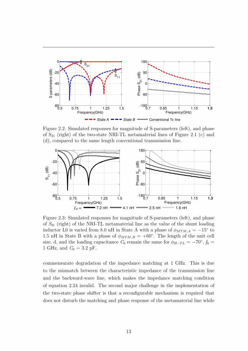
to a higher incurred phase can be seen clearly in Figure 2.3, together with the
12
ϕ
ϕ
Ω
ϕ ϕ
ϕ = −ϕ
ϕ
ϕ−10° at 1 GHzϕ
ϕ
ϕ = −10° ϕϕ
−70°,
0.5 0.75 1 1.25 1.5-80
-60
-40
-20
0
Frequency(GHz)
S-p
ara
me
ters
(d
B)
S11
S21
0.7 0.85 1 1.15 1.31.3-180
-90
0
90
180
Frequency(GHz)
Ph
ase
S21 (
dB
)
4.5State A State B Conventional Tx line
θ
Figure 2.2: Simulated responses for magnitude of S-parameters (left), and phaseof S21 (right) of the two-state NRI-TL metamaterial lines of Figure 2.1 (c) and(d), compared to the same length conventional transmission line.
ϕ
ϕ
Ω
ϕ ϕ
ϕ = −ϕ
ϕ
ϕ−10° at 1 GHzϕ
ϕ
L0 =
ϕ = −10° ϕϕ
−70°,
0.5 0.75 1 1.25 1.5-80
-60
-40
-20
0
Frequency(GHz)
S11 (
dB
)
0.7 0.85 1 1.15 1.31.3-180
-90
0
90
180
Frequency(GHz)
Ph
ase
S21 (
dB
)
7.2 nH 4.1 nH 2.5 nH 1.6 nH
θFigure 2.3: Simulated responses for magnitude of S-parameters (left), and phaseof S21 (right) of the NRI-TL metamaterial line as the value of the shunt loadinginductor L0 is varied from 8.0 nH in State A with a phase of φMTM A = −15 to1.5 nH in State B with a phase of φMTM B = +60. The length of the unit cellsize, d, and the loading capacitance C0 remain the same for φH−TL = −70, f0 =1 GHz, and C0 = 3.2 pF.
commensurate degradation of the impedance matching at 1 GHz. This is due
to the mismatch between the characteristic impedance of the transmission line
and the backward-wave line, which makes the impedance matching condition
of equation 2.24 invalid. The second major challenge in the implementation of
the two-state phase shifter is that a reconfigurable mechanism is required that
does not disturb the matching and phase response of the metamaterial line while
13
switching between the two phase states.
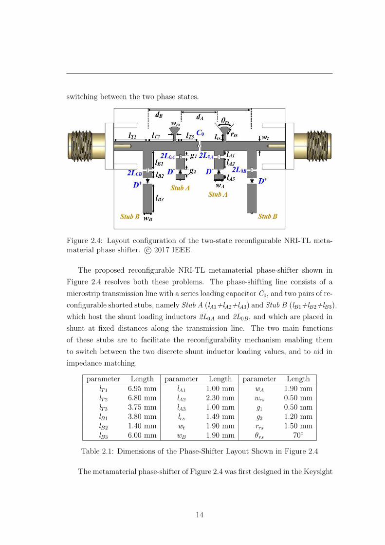
Figure 2.4: Layout configuration of the two-state reconfigurable NRI-TL meta-material phase shifter. c© 2017 IEEE.
The proposed reconfigurable NRI-TL metamaterial phase-shifter shown in
Figure 2.4 resolves both these problems. The phase-shifting line consists of a
microstrip transmission line with a series loading capacitor C0, and two pairs of re-
configurable shorted stubs, namely Stub A (lA1+lA2+lA3) and Stub B (lB1+lB2+lB3),
which host the shunt loading inductors 2L0A and 2L0B, and which are placed in
shunt at fixed distances along the transmission line. The two main functions
of these stubs are to facilitate the reconfigurability mechanism enabling them
to switch between the two discrete shunt inductor loading values, and to aid in
impedance matching.
parameter Length parameter Length parameter LengthlT1 6.95 mm lA1 1.00 mm wA 1.90 mmlT2 6.80 mm lA2 2.30 mm wrs 0.50 mmlT3 3.75 mm lA3 1.00 mm g1 0.50 mmlB1 3.80 mm lrs 1.49 mm g2 1.20 mmlB2 1.40 mm wt 1.90 mm rrs 1.50 mmlB3 6.00 mm wB 1.90 mm θrs 70
Table 2.1: Dimensions of the Phase-Shifter Layout Shown in Figure 2.4
The metamaterial phase-shifter of Figure 2.4 was first designed in the Keysight
14

– Advanced Design System (ADS) simulator to incur an insertion phase in State
A of φMTM A = −15 at 1 GHz using the two central stubs (Stub A), while the
two outer stubs (Stub B) were turned off. Subsequently, the two outer stubs (Stub
B) were turned on, and the two inner ones (Stub A) were turned off while keeping
C 0 constant, in order to achieve an insertion phase in State B of φMTM B = +60
at 1 GHz to achieve a phase difference of 75. In doing so, a similar impedance
matching degradation to the one shown in Figure 2.3(a) was observed. Thus,
Quasi-Newton multivariable optimization was used to match the impedance of
both State A and State B using following algorithm.
2.2.2 Optimization Algorithm
Optimization workspace of Advanced Design System (ADS) was used as the op-
timization tool in this work. Step 1: Design a metamaterial unit cell on a 50 Ω
transmission line with a length = 35 mm with φMTM A = −15 (State A) at 1
GHz and formulate initial C 0 and L0A values.
Step 2: Design stub A with lengths L A1, L A2 and L A3 and gaps to host L0A
and PIN diode with forward polarity.
Step 3: Calculate L0B for φMTM B = +60 (State B) while C 0 is kept the same
as defined in step 1.
Step 4: Design stub B with lengths L B1, L B2 and L B3 and gap to host L0B
and PIN diode with reverse polarity.
Step 5: Evaluate optimized values of the optimization variables using Quasi-
Newton multivariable optimization with the following simultaneous goals:
1. |S11| in state A < −10 dB at 1 GHz
2. |S11| in state B < −10 dB at 1 GHz
3. φMTM A = −15±EA in State A
4. φMTM B = +60±EB in State B
15
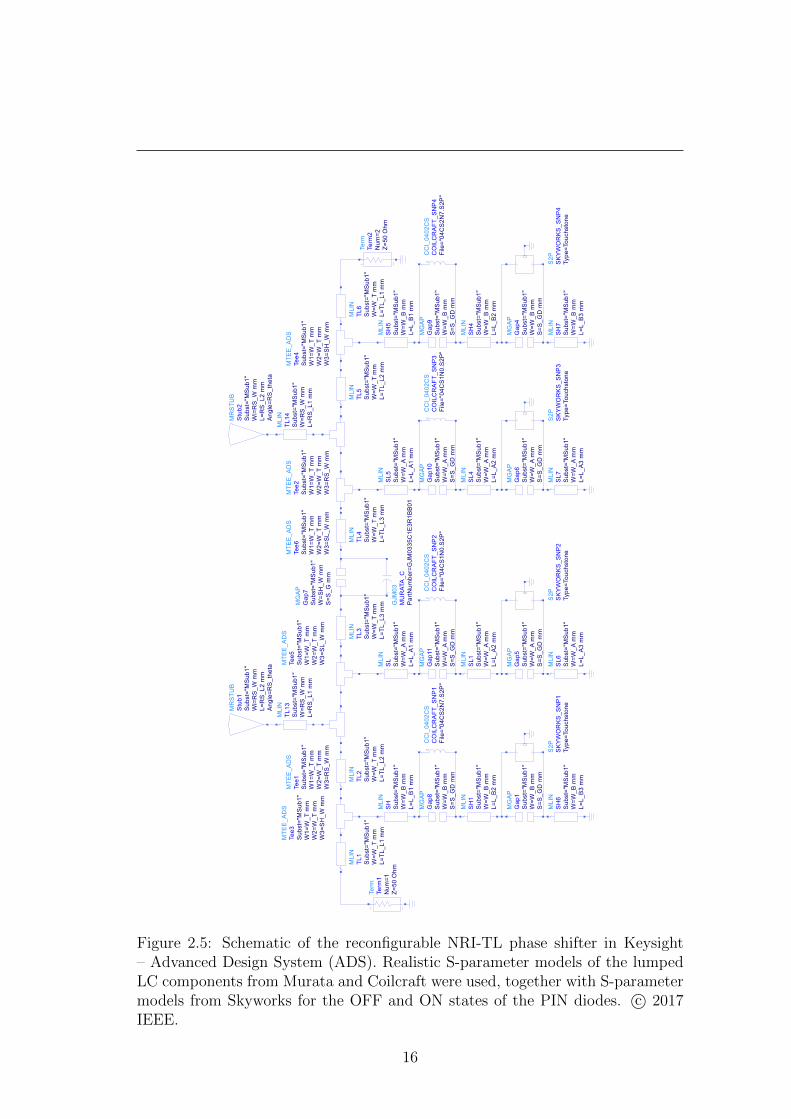
Figure 2.5: Schematic of the reconfigurable NRI-TL phase shifter in Keysight– Advanced Design System (ADS). Realistic S-parameter models of the lumpedLC components from Murata and Coilcraft were used, together with S-parametermodels from Skyworks for the OFF and ON states of the PIN diodes. c© 2017IEEE.
16
5. 2 × (TL L1+TL L2+TL L3) = 35 mm
(Where EA and EB are the tolerance factors in degrees with initial value =
0.5)
If the optimization criteria are satisfied go to the next sequential step. Else go to
step 14.
Step 6: Define optimization variables L B1, LB 2, LB 3, L A1, L A2 and L A3.
Go to step 5. If already optimized, go to next sequential step.
Step 7: Define optimization variables TL L1, TL L2, TL L3. Repeat step 5 and
6. If already optimized, go to next sequential step.
Step 8: Define optimization variables L0A and L0B. Repeat step 5, 6 and 7.
Step 9: Replace the optimized values of L0A and L0B with closest discrete in-
ductance value from the Coilcraft chip inductor library. Repeat step 5, 6 and
7.
Step 10: Define optimization variables C 0. Repeat step 5, 6 and 7.
Step 11: Replace the optimized value of C 0 with closest discrete capacitance
value from the Murata chip capacitor library. Repeat step 5, 6 and 7.
Step 12: Define optimization variables RS L1, RS L2, RS W, RS theta. Repeat
step 5, 6 and 7.
Step 13: Decrease EA and EB values by 0.5. Repeat steps 6-12. If already
optimized in previous iteration, go to step 15.
Step 14: Increase EA and EB values by 0.5. Repeat step 6-12.
Step 15: End
Upon successful completion of the optimization algorithm, the final values of
the lumped components were C 0 = 3.10 pF, L0A = 0.55 nH, L0B = 1.40 nH,
while the optimized geometrical dimensions of the phase shifter are enlisted in
table 2.4. The resulted phase difference between states A and B is 73o.
17
(a) (b)
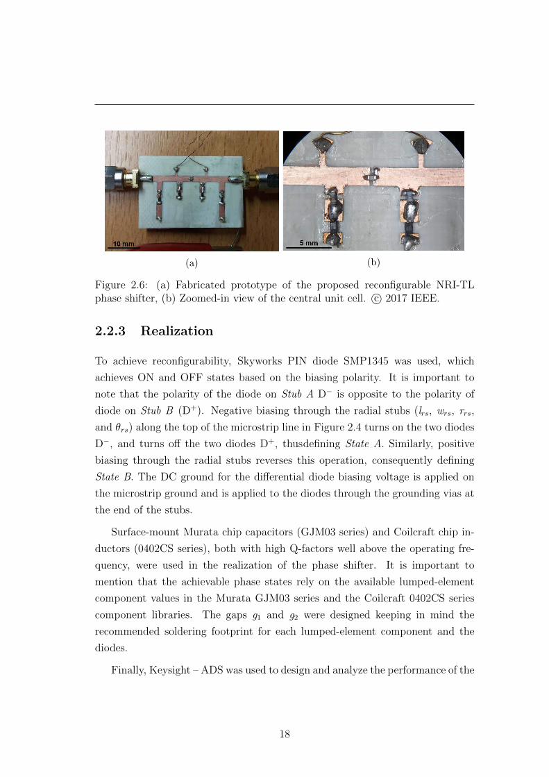
Figure 2.6: (a) Fabricated prototype of the proposed reconfigurable NRI-TLphase shifter, (b) Zoomed-in view of the central unit cell. c© 2017 IEEE.
2.2.3 Realization
To achieve reconfigurability, Skyworks PIN diode SMP1345 was used, which
achieves ON and OFF states based on the biasing polarity. It is important to
note that the polarity of the diode on Stub A D− is opposite to the polarity of
diode on Stub B (D+). Negative biasing through the radial stubs (lrs, wrs, rrs,
and θrs) along the top of the microstrip line in Figure 2.4 turns on the two diodes
D−, and turns off the two diodes D+, thusdefining State A. Similarly, positive
biasing through the radial stubs reverses this operation, consequently defining
State B. The DC ground for the differential diode biasing voltage is applied on
the microstrip ground and is applied to the diodes through the grounding vias at
the end of the stubs.
Surface-mount Murata chip capacitors (GJM03 series) and Coilcraft chip in-
ductors (0402CS series), both with high Q-factors well above the operating fre-
quency, were used in the realization of the phase shifter. It is important to
mention that the achievable phase states rely on the available lumped-element
component values in the Murata GJM03 series and the Coilcraft 0402CS series
component libraries. The gaps g1 and g2 were designed keeping in mind the
recommended soldering footprint for each lumped-element component and the
diodes.
Finally, Keysight – ADS was used to design and analyze the performance of the
18
proposed reconfigurable NRI-TL phase shifter using realistic S-parameter models
for the Murata capacitors, the Coilcraft inductors and the Skyworks diodes, in
conjunction with a realistic model of the physical geometry of the microstrip lines
and gaps on a Rogers RO4003C substrate (εr = 3.38, tanδ = 0.0027, h = 0.813
mm), as can be seen in the full simulation models of Figures 2.4 and 2.5. For a
two-state insertion phase of φMTM A = −15 in State A and of φMTM B = +60
in State B, the final optimized set of loading values was determined to be C 0 =
3.1 pF, 2L0A = 1.1 nH, and 2L0B = 2.8 nH, corresponding to available discrete
values in the Murata GJM03 and the Coilcraft 0402CS component series. It is
worth mentioning here that the total shunt inductances for a particular state is
a combination of the loading inductance (L0A or L0B), the internal inductance of
Skyworks diodes (LPIN = 0.7 nH) and the physical dimensions of the correspond-
ing stubs (Stub A or Stub B). The final layout dimensions of the phase shifter are
also listed in 2.1.
The fabricated prototype of the proposed reconfigurable NRI-TL phase shifter
is presented in Fig 6(a). First, the microstrip conductor and gap patterns shown
of Figure 2.4 were realized on the Rogers RO4003C substrate using a LPKF
ProtoMat H100 milling machine. Holes of 0.4 mm diameter were drilled at the end
of all four stubs for the placement of shorting vias. Then, the lumped components
(C 0, 2L0A and 2L0B) and diodes (D+ and D−) were soldered onto the microstrip
transmission lines, as shown in the zoomed-in view of the central metamaterial
unit cell in Figure 2.6 (b). Finally, SMA connectors were attached for the S-
parameter measurements.
The simulated and measured results of the reconfigurable NRI-TL phase
shifter are shown in Figure 2.7, where it can be observed that there is very
good correlation between the two. The reflection coefficients for both State A
and State B shown in Figure 2.7(a) is well below −10 dB at 1 GHz, indicating
good impedance matching at the design frequency.
19
−
−
− −− −
− −− −
ϕ ϕ
−14.5° and ϕ
(a)
0.5 0.75 1 1.25 1.5-50
-40
-30
-20
-10
0
Frequency(GHz)
S-p
ara
me
ters
(d
B)
State A Meas.
State A Simu.
State B Meas.
State B Simu.
(a)
−
−
− −− −
− −− −
ϕ ϕ
−14.5° and ϕ
(b)
0.5 0.75 1 1.25 1.5-30
-20
-10
0
Frequency(GHz)
S21 (
dB
)
State A Meas.
State A Simu.
State B Meas.
State B Simu.
(b)
−
−
− −− −
− −− −
ϕ ϕ
−14.5° and ϕ
(c)
0.7 0.85 1 1.15 1.31.3-180
-90
0
90
180
Frequency(GHz)
Ph
ase
S21 (
dB
)
State A Meas.
State A Simu.
State B Meas.
State B Simu.
Conventional Tx line
(c)
−
−
− −− −
− −− −
ϕ ϕ
−14.5° and ϕ
(d)
0.7 0.85 1 1.15 1.31.30
1
2
3
Frequency(GHz)
Gro
up
de
lay (
ns)
State A Meas.
State A Simu.
State B Meas.
State B Simu.
(d)
Figure 2.7: (a) Simulated and measured responses of the reconfigurable NRI-TLmetamaterial phase shifter. (a) |S11|, (b) |S21|, (c) Phase of S21, and (d) groupdelay.
20
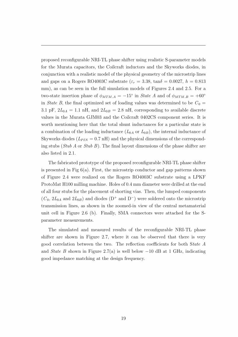
2.2.4 Results and Discussion
At 1 GHz, the simulated and measured |S11| are −18.34 dB and −19.33 dB,
respectively for State A, while they are −29.05 dB and −23.38 dB, respectively
for State B. The advantages achieved by excluding the tuning mechanism from
the direct signal path can be witnessed in terms of the low insertion losses, seen
in Figure 2.7(b). The simulated and measured |S21| are −1.53 dB and −1.43 dB,
respectively for State A, and −0.23 dB and −0.89 dB, respectively for State B. In
Figure 2.7(c), the phase response of an unloaded microstrip line is compared with
the simulated and measured phase responses for both State A and State B. From
Figure 2.7(a), (b) and (c), it can be observed that the reconfigurable NRI-TL
metamaterial phase shifter retains its good impedance matching and transmission
characteristics even though the insertion phase is significantly changed from State
A to State B.
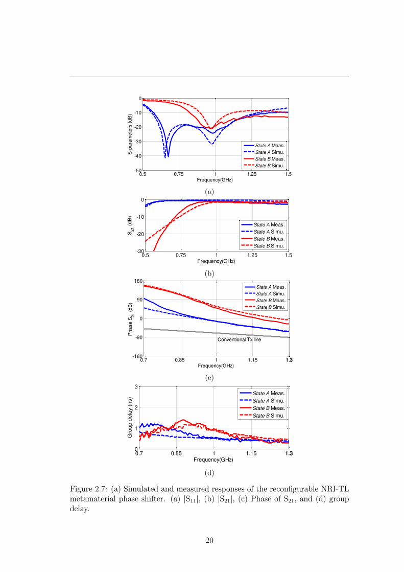
Figure 2.8: Normalized surface current distribution at 1 GHz on the conductorsof the NRI-TL metamaterial phase shifter in State A (left), and State B (right).
Π
Π
Roger’s
ϕ
—
G.V. Eleftheriades, A.K. Iyer, and P.C. Kremer, “Planar negative
lines,” –
–
Eleftheriades, “Transmissionmetamaterials in antenna engineering,” in
. Phase difference between two states.
e
h
± * * *
0.7 0.85 1 1.15 1.31.30
45
90
135
180
Frequency(GHz)
S
21 S
tate
B -
S
21 S
tate
A
Figure 2.9: Measured phase difference between the two states.
21
At 1 GHz, the ideal phase delay is 70, which is compensated by φBW = 55.5
and 128.5 for State A and State B, respectively, resulting in φMTM A = −14.5
and φMTM B = +58.5 at 1 GHz. The measured phase shift deviates by 2.4% and
0.03% from the predicted simulated value for State A and State B, respectively,
which is well within the fabrication tolerances.
The group delay of the reconfigurable NRI-TL phase shifter is shown in Figure
2.7(d), depicting good simulation and measurement agreement for both states.
At 1 GHz, the measured group delay is 0.5 ns for State A, and 0.9 ns for State B,
and these remain relatively flat in the range of 0.4 to 1.3 ns across the operating
band shown. Figure 2.8 shows the surface current distribution on the conductors
of the reconfigurable NRI-TL phase shifter for State A and State B. It can be
observed that the maximum surface current resides within the defined NRI-TL
metamaterial unit cell for a particular state, while the un-used stubs carry an
insignificant amount of surface current, resulting in very good isolation in both
states. The measured phase difference between the two states for the frequency
range of 0.75-1.25 GHz is shown in Figure 2.9, where it can be observed that it
is relatively flat with a value of 73 at 1 GHz that varies between 38.4 to 89.1
in the range shown. Finally, 2.23 summarizes the performance of the proposed
reconfigurable NRI-TL metamaterial phase shifter and other phase shifters found
in the literature, which compares quite favorably. It has the most compact size,
0.07 λ x 0.06 λ, when normalized with respect to the central frequency wavelength,
and the widest bandwidth (18.7%) within which the S21 phase varies less than
±20. Albeit its compact and simple structure, one of the major disadvantages
of the proposed architecture is the discrete phase shift that it can achieve. Other
topologies that have achieved continuous phase tuning capabilities can be found
in literature. An extension of this work would be to apply existing continuous
phase tuning methods to the architecture proposed herein.
22
Ref [6] [7] [11] [14] This workmm×mm 30.0×68.0 10.8×9.4 30.0×40.0 85.5×30.0 17.8×21.6λ × λ 0.19×0.09 0.09×0.08 0.26×0.20 0.57×0.20 0.07×0.06Freq (GHz) 0.9 2.5 2.0 2.0 1.0IL (dB)min-max
4.0-5.6 0.55-1.1 2-10 0.56-0.69 0.89-1.43
Phase rangemin-max
-22 to30
-40 to34
51 to184
313 to355
-14 to59
Bandwidth∠S21±20
0.8-0.9513.5%
2.4-2.711.8%
2.4-2.7513.6%
2-2.083.9%
0.92-1.1118.7%
Technology Micro-fluids
MMIC varactordiode
metallicperturber
PINdiode
Table 2.2: Performance comparison of Reconfigurable NRI-TL Metamaterialbased phase shifters.
2.3 A Compact NRI-TL Metamaterial Microstrip
Crossover
This work demonstrates a practical implementation of a miniaturized microwave
crossover using negative-refractive-index transmission-line (NRI-TL) metamate-
rials. NRI-TL metamaterial theory has demonstrated that by loading a con-
ventional transmission line with lumped LC elements, a large phase shift per-
unit-length can be achieved. Using this feature of NRI-TL metamaterials, the
miniaturization of a crossover has been achieved by replacing the conventional
microstrip transmission lines in a three-section branch-line coupler crossover with
NRI-TL metamaterials lines. A compact NRI-TL crossover with an area 47 times
smaller than the area of the conventional counterpart is presented. Measured re-
sults demonstrate that the proposed NRI-TL Metamaterial crossover exhibits -10
dB |S11| bandwidth of 32.67 % and a |3 dB| |S31| of 25.64 % at around 1 GHz.
Planar microwave circuits frequently use microwave transmission lines that
intersect with each other. A crossover has been a well-known device suited for
such intersection points after its first successful implementation by Weight [6].
Since then, a number of configurations of crossover devices have been presented
to primarily increase the bandwidth of the device and to decrease the overall size
23
24 mm
8 m
m
55 m
m165 mm
MTM crossover
(λ/27 × λ/9)
TL crossover (λ/4 × 3λ/4)
Z0
Z0
Z0
Z0
Z02 Z02Z04
Z02 Z02Z04
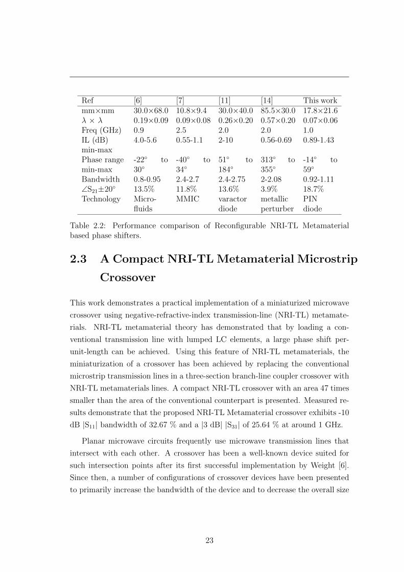
Z01 Z01Z03 Z03
Figure 2.10: Footprint comparison between a microwave crossover using con-ventional transmission lines and a compact NRI-TL metamaterial microwavecrossover.
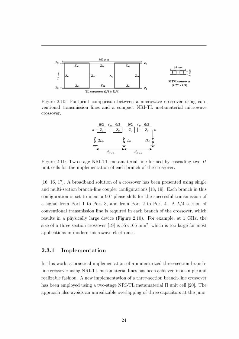
Z0 Z0
C0
2L0
θ/2
dH-TL
Z0 Z0
C0
2L0L0
θ/2 θ/2 θ/2
dH-TL
Figure 2.11: Two-stage NRI-TL metamaterial line formed by cascading two Πunit cells for the implementation of each branch of the crossover.
[16, 16, 17]. A broadband solution of a crossover has been presented using single
and multi-section branch-line coupler configurations [18, 19]. Each branch in this
configuration is set to incur a 90 phase shift for the successful transmission of
a signal from Port 1 to Port 3, and from Port 2 to Port 4. A λ/4 section of
conventional transmission line is required in each branch of the crossover, which
results in a physically large device (Figure 2.10). For example, at 1 GHz, the
size of a three-section crossover [19] is 55×165 mm2, which is too large for most
applications in modern microwave electronics.
2.3.1 Implementation
In this work, a practical implementation of a miniaturized three-section branch-
line crossover using NRI-TL metamaterial lines has been achieved in a simple and
realizable fashion. A new implementation of a three-section branch-line crossover
has been employed using a two-stage NRI-TL metamaterial Π unit cell [20]. The
approach also avoids an unrealizable overlapping of three capacitors at the junc-
24
tions of each branch while using a T-unit cell (for example in [21]). A single
NRI-TL metamaterial Π unit cell consists of a host transmission line with char-
acteristic impedance Z 0, series inductance per unit length L, shunt capacitance
per unit length C, and length d, which is loaded with a lumped-element series
capacitor C 0 and two shunt inductors 2L0. A cascade of two metamaterial Π
unit cells to form a two-stage NRI-TL metamaterial line is presented in Figure
2.11. The conventional host transmission line realizes a negative phase response,
φH−TL, while the series capacitive and shunt inductive loading forms a backward-
wave (BW) line with a positive phase response φBW . Under effective medium
conditions, the phase shift for N NRI-TL metamaterial unit cells is given by [7]:
ΦMTM ≈ N(φMTM) = N
(−ω√LCd+
1
ω√L0C0
)(2.25)
This is valid under the impedance matching condition of 2.24. At the initial de-
sign phase, the impedance of each branch was calculated based on the three stage
branch line coupler presented in [6]. The calculated characteristic impedance val-
ues of the transmission lines were Z 0 = Z 01 = 50 Ω, Z 02 = 45 Ω, and Z 03 =
Z 04 = 81 Ω. Each branch of the original crossover consisted of a 90 microstrip
transmission line, which was replaced with a compact two-stage NRI-TL meta-
material line, where each unit cell had an electrical length of θ = 5. A total
number of 10 such branches formed the three-stage metamaterial crossover. The
lumped components values for each unit cell were calculated using the guidelines
presented in [7] and are enlisted in Table 1 along with the geometrical width of
the host transmission line. The calculated L0 and C 0 simultaneously need to sat-
isfy the conditions of equation 2.25 and 2.24. In total, 20 surface-mount device
(SMD) capacitors and 18 SMD inductors were used to implement the crossover,
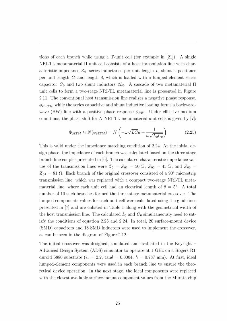
as can be seen in the diagram of Figure 2.12.
The initial crossover was designed, simulated and evaluated in the Keysight –
Advanced Design System (ADS) simulator to operate at 1 GHz on a Rogers RT
duroid 5880 substrate (εr = 2.2, tanδ = 0.0004, h = 0.787 mm). At first, ideal
lumped-element components were used in each branch line to ensure the theo-
retical device operation. In the next stage, the ideal components were replaced
with the closest available surface-mount component values from the Murata chip
25
Figure 2.12: Full-wave EM simulation prototype of the three-section NRI-TLmetamaterial crossover.
capacitor (GJM03 series) and Coilcraft chip inductor (0402CS series) component
libraries. In the next and final stage, a full wave EM simulator was used to eval-
uate the device performance in a realistic environment. Figure 2.12 shows the
geometrical configuration and component loading of the proposed device. It can
be observed that due to the small size of the device, SMA connectors cannot be
mounted directly to the ports of the crossover, therefore 50 Ω curved feed lines
were added, and the SMA connectors were attached to these. The SMD capaci-
tors were mounted in series along with the microstrip line trace, whereas the SMD
inductors were placed vertically through the substrate. When assembling each of
the individually-designed metamaterial branches to form the crossover, a shunt
inductor is present at both ends of each branch, however, at each junction it is
not practically feasible to place adjacently three separate inductors correspond-
ing to separate branches in a very small area. Therefore, an equivalent parallel
inductance has been evaluated (L01 || L02 for a junction of 2 branches and L01
|| L02 || L03 for a junction of 3 branches). The closest possible component value
in the Coilcraft chip inductor (0402CS series) component library has been used
to implement this new equivalent inductance value. Although the crossover was
initially designed at a design frequency of 1 GHz, due to the limited and discrete
range of component values available in the Murata and Coilcraft SMD component
libraries, the final design was optimized at a slightly shifted design frequency of
f 0 = 0.965 GHz.
26
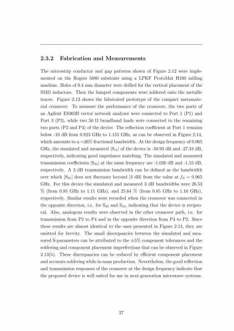
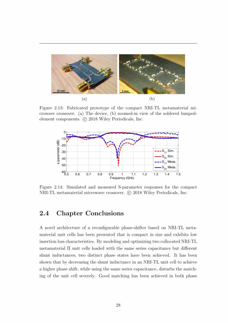
2.3.2 Fabrication and Measurements
The microstrip conductor and gap patterns shown of Figure 2.12 were imple-
mented on the Rogers 5880 substrate using a LPKF ProtoMat H100 milling
machine. Holes of 0.4 mm diameter were drilled for the vertical placement of the
SMD inductors. Then the lumped components were soldered onto the metallic
traces. Figure 2.13 shows the fabricated prototype of the compact metamate-
rial crossover. To measure the performance of the crossover, the two ports of
an Agilent E8363B vector network analyser were connected to Port 1 (P1) and
Port 3 (P3), while two 50 Ω broadband loads were connected to the remaining
two ports (P2 and P4) of the device. The reflection coefficient at Port 1 remains
below -10 dB from 0.823 GHz to 1.155 GHz, as can be observed in Figure 2.14,
which amounts to a ∼26% fractional bandwidth. At the design frequency of 0.965
GHz, the simulated and measured |S11| of the device is -50.93 dB and -27.34 dB,
respectively, indicating good impedance matching. The simulated and measured
transmission coefficients |S31| at the same frequency are -1.026 dB and -1.55 dB,
respectively. A 3 dB transmission bandwidth can be defined as the bandwidth
over which |S31| does not fluctuate beyond |3 dB| from the value at f 0 = 0.965
GHz. For this device the simulated and measured 3 dB bandwidths were 26.53
% (from 0.85 GHz to 1.11 GHz), and 25.64 % (from 0.85 GHz to 1.10 GHz),
respectively. Similar results were recorded when the crossover was connected in
the opposite direction, i.e. for S33 and S13, indicating that the device is recipro-
cal. Also, analogous results were observed in the other crossover path, i.e. for
transmission from P2 to P4 and in the opposite direction from P4 to P2. Since
these results are almost identical to the ones presented in Figure 2.14, they are
omitted for brevity. The small discrepancies between the simulated and mea-
sured S-parameters can be attributed to the ±5% component tolerances and the
soldering and component placement imperfections that can be observed in Figure
2.13(b). These discrepancies can be reduced by efficient component placement
and accurate soldering while in mass production. Nevertheless, the good reflection
and transmission responses of the crossover at the design frequency indicate that
the proposed device is well suited for use in next-generation microwave systems.
27
(a) (b)
Figure 2.13: Fabricated prototype of the compact NRI-TL metamaterial mi-crowave crossover. (a) The device, (b) zoomed-in view of the soldered lumped-element components. c© 2018 Wiley Periodicals, Inc.
0.5 0.6 0.7 0.8 0.9 1 1.1 1.2 1.3 1.4 1.5
-60
-50
-40
-30
-20
-10
0
Frequency (GHz)
s-p
ara
me
ter
(dB
)
S11
Sim.
S31
Sim.
S11
Meas.
S31
Meas.
Figure 2.14: Simulated and measured S-parameter responses for the compactNRI-TL metamaterial microwave crossover. c© 2018 Wiley Periodicals, Inc.
2.4 Chapter Conclusions
A novel architecture of a reconfigurable phase-shifter based on NRI-TL meta-
material unit cells has been presented that is compact in size and exhibits low
insertion loss characteristics. By modeling and optimizing two collocated NRI-TL
metamaterial Π unit cells loaded with the same series capacitance but different
shunt inductances, two distinct phase states have been achieved. It has been
shown that by decreasing the shunt inductance in an NRI-TL unit cell to achieve
a higher phase shift, while using the same series capacitance, disturbs the match-
ing of the unit cell severely. Good matching has been achieved in both phase
28
states by adjusting the length and positions of the inductively-loaded shorted
stubs. The reconfigurable mechanism has been achieved by placing PIN diodes
on four shorted stubs, enabling the device to operate in two phase states based
on the biasing polarity. This also avoids the presence of lossy components in
the direct signal path. The proposed device was fabricated on a 35.5×25 mm2
Rogers RO4003C substrate and the measured results show good agreement with
the simulations. The useable bandwidth of the proposed device for which the
|S11| of both states simultaneously remains below −10 dB is 0.46 GHz (46%),
from 0.83 GHz to 1.29 GHz. In State A, the phase shifter achieves a phase shift
of −14.5, while in State B +58.5, resulting in a measured differential phase shift
of 73 at 1 GHz. The measured |S21| for State A is −1.43 dB, and for State B
−0.89 dB. The realized phase difference is representative, and the same metama-
terial phase-shifting architecture can also be used to achieve any other arbitrary
phase shifting value. Thus, the proposed reconfigurable NRI-TL metamaterial
phase-shifter is ideal for use in feeding networks of next-generation antenna array
systems for pattern and polarization diversity applications. Also, the capability
to achieve high phase differences while maintaining compactness makes it well
suited for use in massive MIMO systems. An effective and practical implemen-
tation of a compact NRI-TL metamaterial microwave crossover is presented in
this work. The overall footprint has been reduced significantly by a factor of
47, while the signal reflection and transmission characteristics of the device are
maintained at a good level. The design frequency of the proposed device around 1
GHz has been selected to enable rapid prototyping using commercially-available
SMD components, however, the same design procedure that has been presented
can be used to design NRI-TL metamaterial crossovers at higher frequencies for
use in future microwave systems such as 5G and beyond. Thus, future work
would involve the replacement of SMD components with inter-digital capacitors
and printed inductors, which can be investigated to further decrease the cost and
losses of the device.
29
Chapter 3
Metasurface Based Miniaturized
Wearable Antenna
In recent years synthesizing new materials with meta-physical properties has been
focused by a number of research efforts. These metamaterials are designed for
better performance of antennas by making use of periodic structures. Special
attention has been given to high impedance surfaces. A specific form of these
surfaces turn out to have frequency bands (bandgaps) inside which surface waves
are reflected rather than being propagated, and they are therefore such specific
metasurfaces are referred to as electromagnetic bandgap (EBG) surfaces. This
chapter presents a planar monopole backed with a 2×1 array of Electromagnetic
Band Gap (EBG) structures. The reflection phase of a single EBG unit cell
has been studied and exploited towards efficient radiation of a planar monopole
antenna, intended for wearable applications. The shape of the EBG unit cell and
the gap between the ground and the EBG layer are adjusted so that the antenna
operates at 2.45 GHz. The proposed antenna retains its impedance matching
when placed directly upon a living human subject with an impedance bandwidth
of 5%, while it exhibits a measured gain of 6.88 dBi. A novel equivalent array
model is presented to qualitatively explain the reported radiation mechanism of
the EBG-backed monopole. The proposed antenna is fabricated on a 68×38×1.57
mm3 board of semi-flexible RT/duroid 5880 substrate. Detailed analysis and
measurements are presented for various cases when the antenna is subjected to
30
structural deformation and human body loading, and in all cases the EBG-backed
monopole antenna retains its high performance. The reported efficient and robust
radiation performance with very low specific absorption rate (SAR), the compact
size, and the high gain, make the proposed antenna a superior candidate for most
wearable applications used for off-body communication.
3.1 Introduction to Metasurfaces
Metasurfaces (MTSs) are the two-dimensional equivalents of volumetric meta-
material engineered to achieve extraordinary electromagnetic properties in 3-
dimensions. Some recent studies have combined the reconfigurablity with meta-
surfaces to achieve multi-dimensional benefits in an attempt to achieve stronger
fields, smaller size and increased controllability. The various tuning mechanisms
of metasurfaces at microwave and photonic level that have been demonstrated in
the literature can be divided into three general categories; 1) electronic switching
2) microfluidics and 3) photonics.
With the concise planar structure, Metasurface can be used in the design of
planar antennas with improved performances. In the design of antennas, operat-
ing frequency, polarization and radiation pattern are the most important charac-
teristics to be considered. With the rapid development of different wireless com-
munications systems, it is highly desirable if one or more of the above-mentioned
antennas characteristics can be reconfigured. In very recent studies, anisotropic
metasurfaces using mechanically controlled reconfiguriblity is used to achieve fre-
quency tuning from 2.55 GHz to 3.45 GHz [22] and polarization tuning is achieved
at 4 GHz [23]. Similarly, piezoelectric actuators are used at 15 GHz at achieve
frequency tuning in [24] while varactors are used for polarization reconfiguriblity
in [25]. Such vast areas of research with variety of tuning mechanism options
have opened up endless possibilities of metasurfaces in antenna applications.
Metasurface made of carefully designed discrete metallic or dielectric elements
with spatially varying characteristics across its surface can direct the flow of
electromagnetic radiation in way similar to optical holograms. Reconfigurable
31
metasurfaces using microfluidics presented in [26, 27] using nematic liquid crys-
tals demonstrated magnetic resonance frequency tuning, while most recently, mi-
crofluidic split-ring resonators (MF-SRR) fabricated inside a flexible elastomeric
material [28] opened up directions toward switchable metamaterials and recon-
figurable devices such as filters, switches, and resonators. Although a lot of work
has not being put forward in this direction, yet substantial efforts are now fo-
cused on developing metasurfaces with switchable and reconfigurable capabilities
in the microwave and optical regions of the spectrum, thus making reconfigurable
photonic devices controllable by external signals a realistic possibility.
The latest developments have shown that optical metasurfaces comprising a
class of optical metasurfaces with a reduced dimensionality can exhibit excep-
tional abilities for controlling the flow of light to achieve the anomalously large
photonic density of states and provide super-resolution imaging. Tuning capa-
bility in planar photonics technology is expected to facilitate new physics and
enhanced functionality for devices [29]. This technology have enabled new ap-
plications in imaging, sensing, data storage, quantum information processing,
and light harvesting. Metasurface represented by a patterned metal-dielectric
layer that is very thin compared with the wavelength of the incident light and
is typically deposited on a supporting substrate [30]. Photonic components with
adjustable parameters optically reconfigured to result in the phase change [31] or
reflectivity/absorption of metasurface [32] has been demonstrated recently. The
functionality of a device based on such a metasurface depends directly on the
effective, surface-confined, optical dispersion.
3.1.1 Possible application of Metamaterial and Metasur-
faces
Metasurfaces has been practically used in wavefront shaping and beam forming
for 4G communication. Impedance matched metasurface to free space are able to
fully control the phase of the transmitted light, also used for beam deflector and
a flat lens with high transmission efficiency for efficient wireless signal diversity.
The metasurfaces for circularly polarized incident wave can control the component
32
of the circularly polarized transmission with the opposite handedness. They can
also helo in phase jumping associated with polarization change created by using
anisotropic, subwavelength scatterers with identical geometric parameters but
spatially varying orientations for wearable antenna applications. Some studies
has shown a linear-to-circular polarization conversion for wireless signal diversity
and linear polarization rotation for wireless signal diversity. Polarization sensitive
metasurfaces that display asymmetric transmission with respect to the direction
of wave propagation can be used for radar communication. Metasurfaces based on
Dielectric resonators for wearable and bio-compatible implantable applications.
Directional scattering metasurfaces can be used for indoor wireless applications.
Beam forming and wavefront control enabled by dielectric metasurfaces can be
implemented for wearable applications. The coupling between free space and
surface waves using metasurfaces can also be exploited for low profile antennas.
Graphene hybrid metasurfaces can be used for next generation material sciences.
Last, but not least, resonance switchable and frequency tunable metasurfaces
seem to show enormous potential in 5G transmitters and base stations.
Current reconfigurable beam shifters uses switchable feeding network for beam
forming of large antenna arrays. It involves the inherent transmission loss of
power from the network of switches. This transmission loss is proportional to
the number of switches involve to achieve a particular phase difference. Recon-
figurable metasurfaces designed beneath the radiating antenna can reflect the
incident waveform in the given direction. Some possible innovations in this do-
main can be:
Reconfigurable metasurface using resonators (split ring, L-shaped) with elec-
tronic switches (PIN, varactor, MEMS) to define a tunable reflection character-
istics for beam forming (inkjet printer and laser milling machine) Reconfigurable
metasurface using resonators (split ring, L-shaped) with fluid channels enabling
microfluids with different material properties to create variations of reflection sur-
face for beam forming (inkjet printer and 3D printer) Reconfigurable merasurface
created by inkjet printed or 3D printed substrate tunable using incident light of
given wavelength to alter the reflection properties of metasurface for beamform-
ing. (inkjet printer and 3D printer).
33
Polarization is one of the most important factor in microwave and optical
signals. Reconfigurable microwave and photonics metasurfaces can be engineered
for polarization tuning in following innovative ways: Inkjet printed resonators
(L-shaped, split ring) on substrate with microfluidic channels placed in the di-
rection of propagation of microwave. Material properties of fluids changing the
characteristics of metasurfaces to alter the polarization of microwave and opti-
cal signal (laser milling machine and inkjet printer) 3D printed substrate with
hollow space for inkjet printing of photoelectric substrate placed in the direction
of propagation of high frequency microwave signals. Dispersion properties of the
substrates tuned by another incident wave to alter to polarization properties of
the metasurface. (inkjet printer, laser milling machine and 3D printer).
3.2 2×1 EBG-backed Planar Monopole Antenna
Design
With the rapid development in communication systems in the past few years, the
area of wireless body area networks (WBAN) has grown significantly, support-
ing a large number of applications, including personalized health care systems,
patient monitoring systems, rescue systems, battle field survival, and wearable
gaming consoles [33], [34] . Several frequency bands have been allocated for these
applications to commercialize WBAN communication systems, which include the
Medical Implantable Communication Systems (MICS) band (402-405 MHz), In-
dustrial Scientific and Medical (ISM) band (2.40-2.48 GHz) and Ultra Wideband
(UWB). For optimum performance, the antennas used for WBAN applications are
required to be compact, mechanically robust, lightweight and preferably comfort-
able while being worn. It has been reported, that the performance of an antenna
may degrade significantly while operating in close proximity with the human
body [33, 34]. This occurs because the antenna’s surface currents are affected by
the near field coupling with the body, which in turn affects the input impedance
matching of the antenna. Specifically, for narrow-band operation, the dominant
effect of the body proximity is a shift of the resonance frequency, which causes a
mismatch at the designed frequency, resulting in a significant degradation of the
34
total efficiency (Pradiated/Pincident). Designing a narrowband wearable antenna
with a high total efficiency can be a challenging task, especially when it is also
expected for the antenna to have low-profile, conformal and lightweight charac-
teristics [34]. At the same time, the effect of wearable antennas on the human
body in terms of maximum allowable specific absorption rate (SAR) needs to
be addressed [35]. So far a number of configurations have been investigated as
potential candidates for wearable antennas including fractal [36], inverted-F [37],
planar monopoles [38, 39, 40], magneto electric dipoles [41], cavity backed [42],
[43], and stacked microstrip antennas [44].
The microstrip antenna presented in [44], and the cavity backed antennas
[42], [43], can be considered good potential candidates for wearable applica-
tions, however they do not exhibit conformal characteristics. Several textile-
based conformal antennas, including a wearable magneto electric dipole [41], a
fully grounded microstrip [45], textile fractal [36] and textile antenna based on
Substrate-Integrated Waveguide (SIW) technology [46] are proposed to be pli-
able for off-body communication, however they have a relatively large footprint.
A recent investigation on a compact conformal inverted-F wearable antenna has
been presented [37]; however, due to its near-omnidirectional radiation proper-
ties, a significant amount of energy is directed towards the human body. In an
attempt to direct the antenna radiation away from the body for off-body com-
munication with a BAN base station like the one presented in [47], it is always
desirable to have a full ground plane. The presence of a ground plane also in-
creases the isolation between the wearable antenna and the body, thus resulting
in lower SAR values [48]. Other than conventional full or extended ground planes
[44, 45, 49, 50], periodically loaded configurations using high impedance surfaces
[51, 52], artificial magnetic conductors and electromagnetic/photonic band gap
structures [38, 39, 51, 53, 54, 55] have been investigated to introduce improved
isolation between the radiating wearable antenna and living human tissues. How-
ever, these configurations still suffer from frequency shifts due to either bending,
or crumpling, or they have relatively large lateral sizes. In this paper, we present
the novel design of a very compact EBG-backed planar monopole antenna and
the experimental realization of a conformal low-profile wearable antenna operat-
ing at 2.45 GHz in the ISM band. It is worth mentioning here that contrary to
35
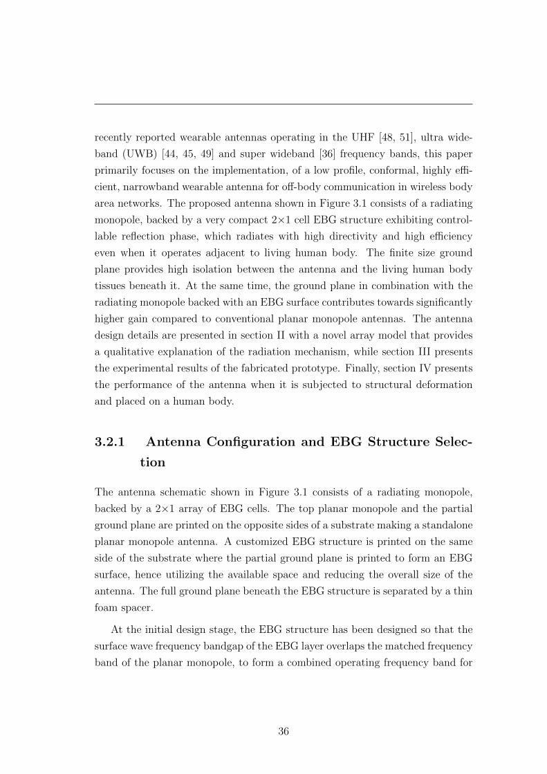
recently reported wearable antennas operating in the UHF [48, 51], ultra wide-
band (UWB) [44, 45, 49] and super wideband [36] frequency bands, this paper
primarily focuses on the implementation, of a low profile, conformal, highly effi-
cient, narrowband wearable antenna for off-body communication in wireless body
area networks. The proposed antenna shown in Figure 3.1 consists of a radiating
monopole, backed by a very compact 2×1 cell EBG structure exhibiting control-
lable reflection phase, which radiates with high directivity and high efficiency
even when it operates adjacent to living human body. The finite size ground
plane provides high isolation between the antenna and the living human body
tissues beneath it. At the same time, the ground plane in combination with the
radiating monopole backed with an EBG surface contributes towards significantly
higher gain compared to conventional planar monopole antennas. The antenna
design details are presented in section II with a novel array model that provides
a qualitative explanation of the radiation mechanism, while section III presents
the experimental results of the fabricated prototype. Finally, section IV presents
the performance of the antenna when it is subjected to structural deformation
and placed on a human body.
3.2.1 Antenna Configuration and EBG Structure Selec-
tion
The antenna schematic shown in Figure 3.1 consists of a radiating monopole,
backed by a 2×1 array of EBG cells. The top planar monopole and the partial
ground plane are printed on the opposite sides of a substrate making a standalone
planar monopole antenna. A customized EBG structure is printed on the same
side of the substrate where the partial ground plane is printed to form an EBG
surface, hence utilizing the available space and reducing the overall size of the
antenna. The full ground plane beneath the EBG structure is separated by a thin
foam spacer.
At the initial design stage, the EBG structure has been designed so that the
surface wave frequency bandgap of the EBG layer overlaps the matched frequency
band of the planar monopole, to form a combined operating frequency band for
36
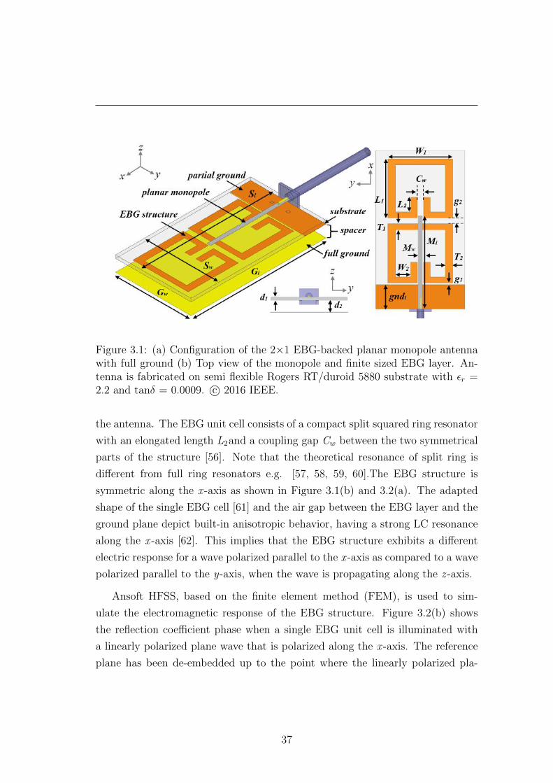
Figure 3.1: (a) Configuration of the 2×1 EBG-backed planar monopole antennawith full ground (b) Top view of the monopole and finite sized EBG layer. An-tenna is fabricated on semi flexible Rogers RT/duroid 5880 substrate with εr =2.2 and tanδ = 0.0009. c© 2016 IEEE.
the antenna. The EBG unit cell consists of a compact split squared ring resonator
with an elongated length L2and a coupling gap Cw between the two symmetrical
parts of the structure [56]. Note that the theoretical resonance of split ring is
different from full ring resonators e.g. [57, 58, 59, 60].The EBG structure is
symmetric along the x -axis as shown in Figure 3.1(b) and 3.2(a). The adapted
shape of the single EBG cell [61] and the air gap between the EBG layer and the
ground plane depict built-in anisotropic behavior, having a strong LC resonance
along the x -axis [62]. This implies that the EBG structure exhibits a different
electric response for a wave polarized parallel to the x -axis as compared to a wave
polarized parallel to the y-axis, when the wave is propagating along the z -axis.
Ansoft HFSS, based on the finite element method (FEM), is used to sim-
ulate the electromagnetic response of the EBG structure. Figure 3.2(b) shows
the reflection coefficient phase when a single EBG unit cell is illuminated with
a linearly polarized plane wave that is polarized along the x -axis. The reference
plane has been de-embedded up to the point where the linearly polarized pla-
37
(a)
1.8 2 2.2 2.4 2.6 2.8 3-180
-135
-90
-45
0
45
90
135
180
Frequency (GHz)
Re
fle
ctio
n P
ha
se
(d
eg
ree
)
d2 = 2 mm
d2 = 5 mm
d2= 8 mm
d2 = 11 mm
(b)
(c)
1.8 2 2.2 2.4 2.6 2.8 3-180
-135
-90
-45
0
45
90
135
180
Frequency (GHz)
Re
fle
ctio
n P
ha
se
(d
eg
ree
)
d2 = 2 mm
d2 = 5 mm
d2= 8 mm
d2 = 11 mm
(d)
Figure 3.2: (a) Configuration of a single unit cell consisting of the EBG elementwith metallic backing under plane wave excitation. (b) Reflection phase of aninfinite array of the EBG unit cells. (d) Configuration of a 21 array of EBG cellsunder plane wave excitation (d) Reflection phase of the 21 array of EBG cells
nar monopole will be located. The structural parameters of the EBG structure,
namely, L1,L2, W1, W2, T1, T2 and Cw were optimized to define the EBG surface
wave frequency band gap. The designated reflection phase for the EBG structure
operation agrees well with the work presented in [63, 64], which argues that it is
advantageous in terms of the antenna impedance matching to work in the region
where the reflection phase of the EBG plane is 90±45. The defining parameter
for this 90±45 bandwidth is the gap between EBG structure and ground plane
(d2) which provides direct control over the reflection phase of the EBG struc-
ture (see Figure 3.2(b)). In [63] it was also concluded that the operational EBG
38
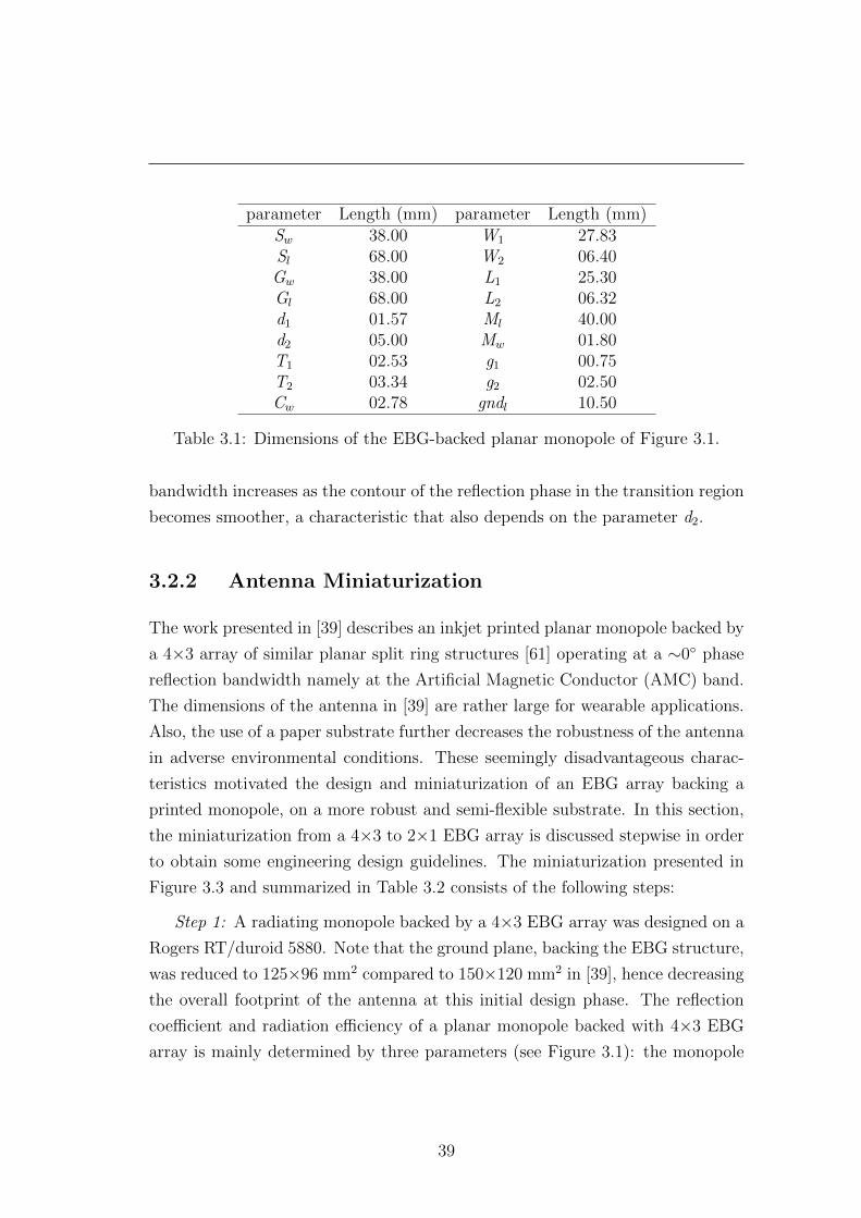
parameter Length (mm) parameter Length (mm)Sw 38.00 W1 27.83Sl 68.00 W2 06.40
Gw 38.00 L1 25.30Gl 68.00 L2 06.32d1 01.57 Ml 40.00d2 05.00 Mw 01.80T1 02.53 g1 00.75T2 03.34 g2 02.50Cw 02.78 gndl 10.50
Table 3.1: Dimensions of the EBG-backed planar monopole of Figure 3.1.
bandwidth increases as the contour of the reflection phase in the transition region
becomes smoother, a characteristic that also depends on the parameter d2.
3.2.2 Antenna Miniaturization
The work presented in [39] describes an inkjet printed planar monopole backed by
a 4×3 array of similar planar split ring structures [61] operating at a ∼0 phase
reflection bandwidth namely at the Artificial Magnetic Conductor (AMC) band.
The dimensions of the antenna in [39] are rather large for wearable applications.
Also, the use of a paper substrate further decreases the robustness of the antenna
in adverse environmental conditions. These seemingly disadvantageous charac-
teristics motivated the design and miniaturization of an EBG array backing a
printed monopole, on a more robust and semi-flexible substrate. In this section,
the miniaturization from a 4×3 to 2×1 EBG array is discussed stepwise in order
to obtain some engineering design guidelines. The miniaturization presented in
Figure 3.3 and summarized in Table 3.2 consists of the following steps:
Step 1: A radiating monopole backed by a 4×3 EBG array was designed on a
Rogers RT/duroid 5880. Note that the ground plane, backing the EBG structure,
was reduced to 125×96 mm2 compared to 150×120 mm2 in [39], hence decreasing
the overall footprint of the antenna at this initial design phase. The reflection
coefficient and radiation efficiency of a planar monopole backed with 4×3 EBG
array is mainly determined by three parameters (see Figure 3.1): the monopole
39
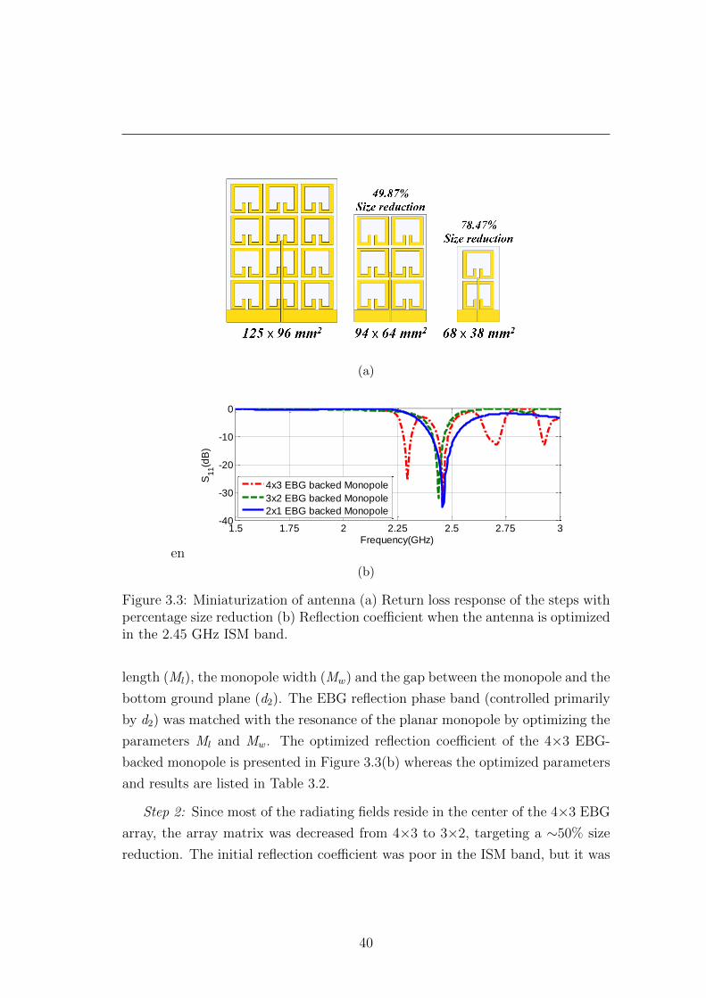
(a)
en
1.5 1.75 2 2.25 2.5 2.75 3-40
-30
-20
-10
0
Frequency(GHz)
S11(d
B)
4x3 EBG backed Monopole
3x2 EBG backed Monopole
2x1 EBG backed Monopole
(b)
Figure 3.3: Miniaturization of antenna (a) Return loss response of the steps withpercentage size reduction (b) Reflection coefficient when the antenna is optimizedin the 2.45 GHz ISM band.
length (Ml), the monopole width (Mw) and the gap between the monopole and the
bottom ground plane (d2). The EBG reflection phase band (controlled primarily
by d2) was matched with the resonance of the planar monopole by optimizing the
parameters Ml and Mw. The optimized reflection coefficient of the 4×3 EBG-
backed monopole is presented in Figure 3.3(b) whereas the optimized parameters
and results are listed in Table 3.2.
Step 2: Since most of the radiating fields reside in the center of the 4×3 EBG
array, the array matrix was decreased from 4×3 to 3×2, targeting a ∼50% size
reduction. The initial reflection coefficient was poor in the ISM band, but it was
40
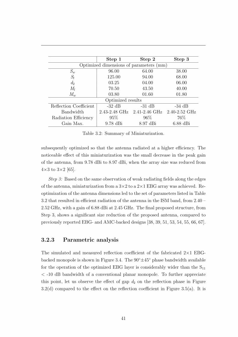
Step 1 Step 2 Step 3Optimized dimensions of parameters (mm)
Sw 96.00 64.00 38.00Sl 125.00 94.00 68.00d2 03.25 04.00 06.00Ml 70.50 43.50 40.00Mw 03.80 01.60 01.80
Optimized resultsReflection Coefficient -32 dB -31 dB -34 dB
Bandwidth 2.43-2.48 GHz 2.41-2.46 GHz 2.40-2.52 GHzRadiation Efficiency 95% 96% 76%
Gain Max. 9.78 dBi 8.97 dBi 6.88 dBi
Table 3.2: Summary of Miniaturization.
subsequently optimized so that the antenna radiated at a higher efficiency. The
noticeable effect of this miniaturization was the small decrease in the peak gain
of the antenna, from 9.78 dBi to 8.97 dBi, when the array size was reduced from
4×3 to 3×2 [65].
Step 3: Based on the same observation of weak radiating fields along the edges
of the antenna, miniaturization from a 3×2 to a 2×1 EBG array was achieved. Re-
optimization of the antenna dimensions led to the set of parameters listed in Table
3.2 that resulted in efficient radiation of the antenna in the ISM band, from 2.40 –
2.52 GHz, with a gain of 6.88 dBi at 2.45 GHz. The final proposed structure, from
Step 3, shows a significant size reduction of the proposed antenna, compared to
previously reported EBG- and AMC-backed designs [38, 39, 51, 53, 54, 55, 66, 67].
3.2.3 Parametric analysis
The simulated and measured reflection coefficient of the fabricated 2×1 EBG-
backed monopole is shown in Figure 3.4. The 90±45 phase bandwidth available
for the operation of the optimized EBG layer is considerably wider than the S11
< -10 dB bandwidth of a conventional planar monopole. To further appreciate
this point, let us observe the effect of gap d2 on the reflection phase in Figure
3.2(d) compared to the effect on the reflection coefficient in Figure 3.5(a). It is
41
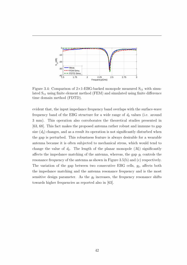
1.5 1.75 2 2.25 2.5 2.75 3-40
-30
-20
-10
0
Frequency(GHz)
S11(d
B)
Meas.
FEM Simu.
FDTD Simu.
Figure 3.4: Comparison of 2×1-EBG-backed monopole measured S11 with simu-lated S11 using finite element method (FEM) and simulated using finite differencetime domain method (FDTD).
evident that, the input impedance frequency band overlaps with the surface-wave
frequency band of the EBG structure for a wide range of d2 values (i.e. around
3 mm). This operation also corroborates the theoretical studies presented in
[63, 68]. This fact makes the proposed antenna rather robust and immune to gap
size (d2) changes, and as a result its operation is not significantly disturbed when
the gap is perturbed. This robustness feature is always desirable for a wearable
antenna because it is often subjected to mechanical stress, which would tend to
change the value of d2. The length of the planar monopole (Ml) significantly
affects the impedance matching of the antenna, whereas, the gap g1 controls the
resonance frequency of the antenna as shown in Figure 3.5(b) and (c) respectively.
The variation of the gap between two consecutive EBG cells, g2, affects both
the impedance matching and the antenna resonance frequency and is the most
sensitive design parameter. As the g2 increases, the frequency resonance shifts
towards higher frequencies as reported also in [63].
42
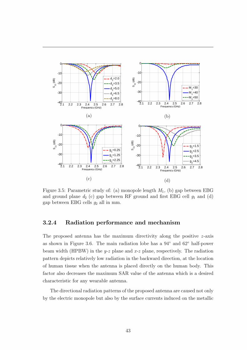
2.1 2.2 2.3 2.4 2.5 2.6 2.7 2.8-40
-30
-20
-10
0
Frequency (GHz)
S11 (
dB
)
d2=2.0
d2=3.5
d2=5.0
d2=6.5
d2=8.0
(a)
2.1 2.2 2.3 2.4 2.5 2.6 2.7 2.8-40
-30
-20
-10
0
Frequency (GHz)
S11 (
dB
)
M1=30
M1=40
M1=50
(b)
2.1 2.2 2.3 2.4 2.5 2.6 2.7 2.8-40
-30
-20
-10
0
Frequency (GHz)
S11 (
dB
)
g1=0.25
g1=1.25
g1=2.25
(c)
2.1 2.2 2.3 2.4 2.5 2.6 2.7 2.8-40
-30
-20
-10
0
Frequency (GHz)
S11 (
dB
)
g2=1.5
g2=2.5
g2=3.5
g2=4.5
(d)
Figure 3.5: Parametric study of: (a) monopole length M1, (b) gap between EBGand ground plane d2 (c) gap between RF ground and first EBG cell g1 and (d)gap between EBG cells g2 all in mm.
3.2.4 Radiation performance and mechanism
The proposed antenna has the maximum directivity along the positive z -axis
as shown in Figure 3.6. The main radiation lobe has a 94 and 62 half-power
beam width (HPBW) in the y-z plane and x-z plane, respectively. The radiation
pattern depicts relatively low radiation in the backward direction, at the location
of human tissue when the antenna is placed directly on the human body. This
factor also decreases the maximum SAR value of the antenna which is a desired
characteristic for any wearable antenna.
The directional radiation patterns of the proposed antenna are caused not only
by the electric monopole but also by the surface currents induced on the metallic
43
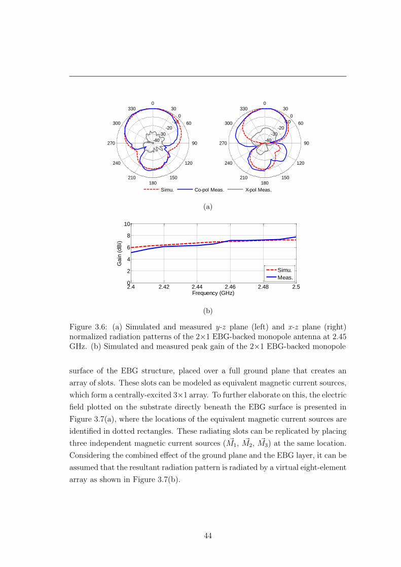
0
-10
-20
-30
-40
030
60
90
120
150180
210
240
270
300
330
0
-10
-20
-30
-40
030
60
90
120
150180
210
240
270
300
330
0-10
-20-30
-40
030
60
90
120
150180
210
240
270
300
330
Simu. Co-pol Meas. X-pol Meas.
(a)
2.4 2.42 2.44 2.46 2.48 2.50
2
4
6
8
10
Frequency (GHz)
Gain
(dB
i)
Simu.
Meas.
(b)
Figure 3.6: (a) Simulated and measured y-z plane (left) and x-z plane (right)normalized radiation patterns of the 2×1 EBG-backed monopole antenna at 2.45GHz. (b) Simulated and measured peak gain of the 2×1 EBG-backed monopole
surface of the EBG structure, placed over a full ground plane that creates an
array of slots. These slots can be modeled as equivalent magnetic current sources,
which form a centrally-excited 3×1 array. To further elaborate on this, the electric
field plotted on the substrate directly beneath the EBG surface is presented in
Figure 3.7(a), where the locations of the equivalent magnetic current sources are
identified in dotted rectangles. These radiating slots can be replicated by placing
three independent magnetic current sources ( ~M1, ~M2, ~M3) at the same location.
Considering the combined effect of the ground plane and the EBG layer, it can be
assumed that the resultant radiation pattern is radiated by a virtual eight-element
array as shown in Figure 3.7(b).
44
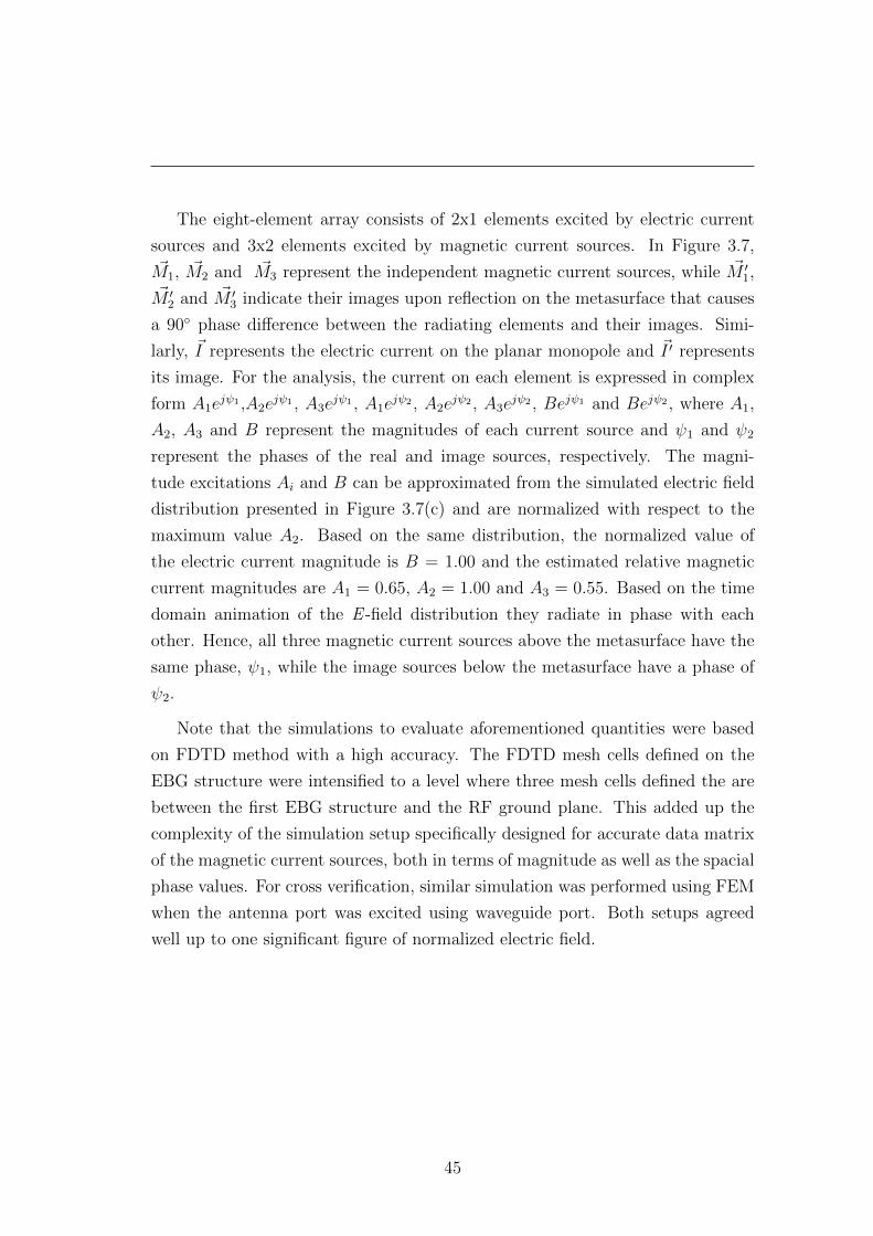
The eight-element array consists of 2x1 elements excited by electric current
sources and 3x2 elements excited by magnetic current sources. In Figure 3.7,~M1, ~M2 and ~M3 represent the independent magnetic current sources, while ~M ′
1,~M ′2 and ~M ′
3 indicate their images upon reflection on the metasurface that causes
a 90 phase difference between the radiating elements and their images. Simi-
larly, ~I represents the electric current on the planar monopole and ~I ′ represents
its image. For the analysis, the current on each element is expressed in complex
form A1ejψ1 ,A2e
jψ1 , A3ejψ1 , A1e
jψ2 , A2ejψ2 , A3e
jψ2 , Bejψ1 and Bejψ2 , where A1,
A2, A3 and B represent the magnitudes of each current source and ψ1 and ψ2
represent the phases of the real and image sources, respectively. The magni-
tude excitations Ai and B can be approximated from the simulated electric field
distribution presented in Figure 3.7(c) and are normalized with respect to the
maximum value A2. Based on the same distribution, the normalized value of
the electric current magnitude is B = 1.00 and the estimated relative magnetic
current magnitudes are A1 = 0.65, A2 = 1.00 and A3 = 0.55. Based on the time
domain animation of the E -field distribution they radiate in phase with each
other. Hence, all three magnetic current sources above the metasurface have the
same phase, ψ1, while the image sources below the metasurface have a phase of
ψ2.
Note that the simulations to evaluate aforementioned quantities were based
on FDTD method with a high accuracy. The FDTD mesh cells defined on the
EBG structure were intensified to a level where three mesh cells defined the are
between the first EBG structure and the RF ground plane. This added up the
complexity of the simulation setup specifically designed for accurate data matrix
of the magnetic current sources, both in terms of magnitude as well as the spacial
phase values. For cross verification, similar simulation was performed using FEM
when the antenna port was excited using waveguide port. Both setups agreed
well up to one significant figure of normalized electric field.
45
(a)
(b)
0 17 34 51 680
0.5
1
Antenna Length along x-axis (mm)
no
rma
lize
d E
-fie
ld (
dB
)
d3
A1
A2
d3
A3
(c)
0
-20
-40
030
60
90
120
150180
210
240
270
300
330
x-z plane y-z plane
(d)
Figure 3.7: (a) Electric field distribution on EBG surface depicting three magneticcurrent sources at 2.45 GHz (b) Equivalent eight-element array model consistingof two electric current sources and six magnetic current sources, (c) Simulatedelectric field on the EBG layer along the x -axis, which is used to model themagnitude of the magnetic current sources, (d) Simulated electric field patternof a ∼λ/4 magnetic current source.
46
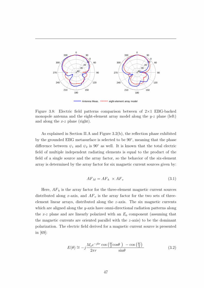
0
-10
-20
-30
-40
030
60
90
120
150180
210
240
270
300
330
0
-10
-20
-30
-40
030
60
90
120
150180
210
240
270
300
330
2.2 2.3 2.4 2.5 2.6 2.7 2.8-25
-20
-15
-10
-5
0
Frequency (GHz)
S11 (
dB
)
Antenna Meas. eight-element array model
Figure 3.8: Electric field patterns comparison between of 2×1 EBG-backedmonopole antenna and the eight-element array model along the y-z plane (left)and along the x-z plane (right).
As explained in Section II.A and Figure 3.2(b), the reflection phase exhibited
by the grounded EBG metasurface is selected to be 90, meaning that the phase
difference between ψ1 and ψ2 is 90 as well. It is known that the total electric
field of multiple independent radiating elements is equal to the product of the
field of a single source and the array factor, so the behavior of the six-element
array is determined by the array factor for six magnetic current sources given by:
AFM = AF h × AF v (3.1)
Here, AF h is the array factor for the three-element magnetic current sources
distributed along x -axis, and AF v is the array factor for the two sets of three-
element linear arrays, distributed along the z -axis. The six magnetic currents
which are aligned along the y-axis have omni-directional radiation patterns along
the x-z plane and are linearly polarized with an Eφ component (assuming that
the magnetic currents are oriented parallel with the z -axis) to be the dominant
polarization. The electric field derived for a magnetic current source is presented
in [69]:
E(θ) ∼= −jMoe
−jkr
2πr
cos(kl2
cosθ)− cos
(kl2
)sinθ
(3.2)
47
Where k is the wavenumber, r is the distance from the source centre, and Mo
is the amplitude of the magnetic current excitation. Considering the “global”
axes presented in Figure 3.7(b), this coincides with the Eθ polarization. The po-
larization of the radiated field is in agreement with the measured co-polarization.
However, for the calculation of the E -field along the y-z plane, the normalized
distribution of the individual magnetic currents has to be considered. The nor-
malized array factor pattern is calculated for an arrangement replicating the
radiating mechanism of the proposed 2×1 EBG-backed monopole, where, d2 =
5.8 mm (∼λ/20) and d3 = 26.7 mm (∼λ/4). The calculated array factor for the
magnetic current sources, AFM , is then superimposed with the radiation pattern
of the remaining 2×1 monopole elements represented by ~I and ~I ′ to form a radia-
tion pattern for an eight-element array model. It should be noted that despite the
fact that the orientation of the 2×1 electric currents is orthogonal with the orien-
tation of the 3×2 magnetic currents, their dominant radiated E -field polarization
coincides because they are excited by electric and magnetic sources respectively.
In both Figures 3.8(a) and (b), the solid lines show the co-polarized measured
radiation patterns of the 2×1 EBG-backed monopole, whereas the dotted lines
show the calculated E -field pattern of the combined eight-element current source
array model. The location of the nulls in Figure 3.8(a) for the eight-element
model is exactly at 90 and 270, which do not coincide exactly with the nulls in
the measured radiation pattern (blue solid contour). This discrepancy is mostly
because of the approximation of the limited size ground plane Gl×Gw with an
ideal infinite ground plane for the eight-element array. Other than the slight re-
location of nulls, it can be observed that the suggested radiation mechanism of
the eight-element array is in very good agreement with the measured radiation
patterns of the fabricated 2×1 EBG-backed monopole. This verifies the validity
of the presented eight-element array model presented in Figure 3.7(b) and also
demonstrates the effect of the metasurface that causes the intended 90o phase
difference between the physical radiators and their images.
48
3.2.5 Experimental Results
The 2×1 EBG-backed monopole was fabricated on an LPKF ProtoMat H 100
milling machine. Styrofoam with the prescribed thickness was added as a spacer
between the EBG layer and the finite ground plane (Figure 3.9). An Agilent
E8363B network analyzer was used to characterize the reflection coefficient of the
antenna in free space. As shown in Figure 3.5(a), good agreement can be seen
between measurements and simulated predictions not only in terms of resonance
position, but also with respect to the 10 dB bandwidth. The measured reflection
coefficient of the 2×1 EBG-backed monopole antenna has a -10 dB bandwidth
ranging from 2.40 to 2.50 GHz, which is slightly narrower than the simulated
response. This small discrepancy between the measurement and simulation can
be related to the additional Ohmic losses normally generated while soldering the
SMA connector on the fabricated prototype.
The measured co-polarized and cross-polarized radiation patterns compared
to the simulations are shown in Figure 3.6. The measurements were taken in an
anechoic chamber at the Idvorski Laboratories Serbia, co-owned by the School
of Electrical Engineering, University of Belgrade. The antenna was placed on
an automatic rotating platform (Figure 3.9(d) and (e)) and gain patterns were
measured at 11 discrete frequency points from 2.4 to 2.5 GHz as shown in Figure
3.6(c). Simulation and measurements are in good agreement. It can be observed
that the antenna retains a reasonable directional radiation pattern in the +z
hemisphere, confirming the simulation predictions. In the x-z plane radiation
pattern, the measured HPBW agrees well with the simulated predictions, which
is around 93. In the y-z plane radiation pattern, the measured HPBW of the
2×1 EBG-backed monopole antenna is 56 (slightly narrower than the simulated
HPBW) and a shift in the maximum directivity is also observed, but predomi-
nantly this was due to fabrication and measurement setup imperfections. Never-
theless, the measured directional radiation patterns confirm the reliable radiation
performance of the proposed wearable antenna.
49
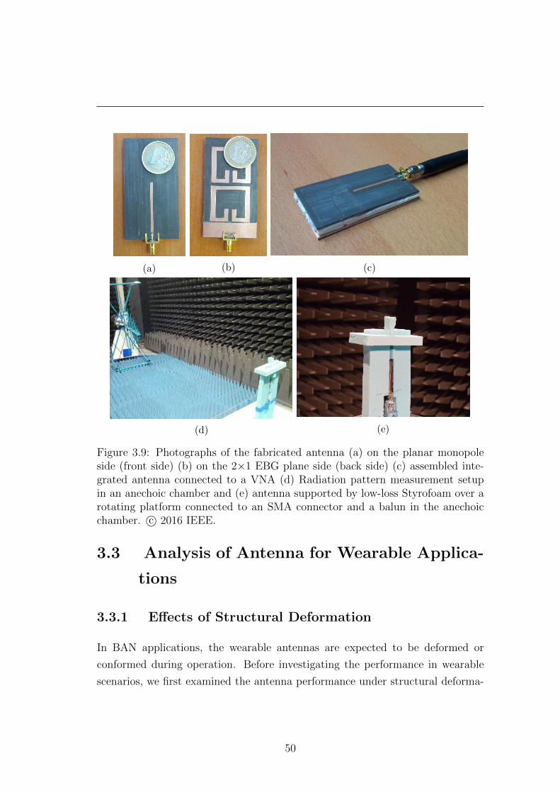
(a)
(b)
(c)
(d)
(e)
Figure 3.9: Photographs of the fabricated antenna (a) on the planar monopoleside (front side) (b) on the 2×1 EBG plane side (back side) (c) assembled inte-grated antenna connected to a VNA (d) Radiation pattern measurement setupin an anechoic chamber and (e) antenna supported by low-loss Styrofoam over arotating platform connected to an SMA connector and a balun in the anechoicchamber. c© 2016 IEEE.
3.3 Analysis of Antenna for Wearable Applica-
tions
3.3.1 Effects of Structural Deformation
In BAN applications, the wearable antennas are expected to be deformed or
conformed during operation. Before investigating the performance in wearable
scenarios, we first examined the antenna performance under structural deforma-
50
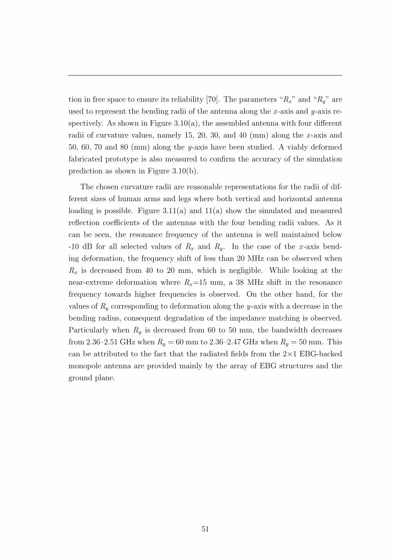
tion in free space to ensure its reliability [70]. The parameters “Rx” and “Ry” are
used to represent the bending radii of the antenna along the x -axis and y-axis re-
spectively. As shown in Figure 3.10(a), the assembled antenna with four different
radii of curvature values, namely 15, 20, 30, and 40 (mm) along the x -axis and
50, 60, 70 and 80 (mm) along the y-axis have been studied. A viably deformed
fabricated prototype is also measured to confirm the accuracy of the simulation
prediction as shown in Figure 3.10(b).
The chosen curvature radii are reasonable representations for the radii of dif-
ferent sizes of human arms and legs where both vertical and horizontal antenna
loading is possible. Figure 3.11(a) and 11(a) show the simulated and measured
reflection coefficients of the antennas with the four bending radii values. As it
can be seen, the resonance frequency of the antenna is well maintained below
-10 dB for all selected values of Rx and Ry. In the case of the x -axis bend-
ing deformation, the frequency shift of less than 20 MHz can be observed when
Rx is decreased from 40 to 20 mm, which is negligible. While looking at the
near-extreme deformation where Rx=15 mm, a 38 MHz shift in the resonance
frequency towards higher frequencies is observed. On the other hand, for the
values of Ry corresponding to deformation along the y-axis with a decrease in the
bending radius, consequent degradation of the impedance matching is observed.
Particularly when Ry is decreased from 60 to 50 mm, the bandwidth decreases
from 2.36–2.51 GHz when Ry = 60 mm to 2.36–2.47 GHz when Ry = 50 mm. This
can be attributed to the fact that the radiated fields from the 2×1 EBG-backed
monopole antenna are provided mainly by the array of EBG structures and the
ground plane.
51
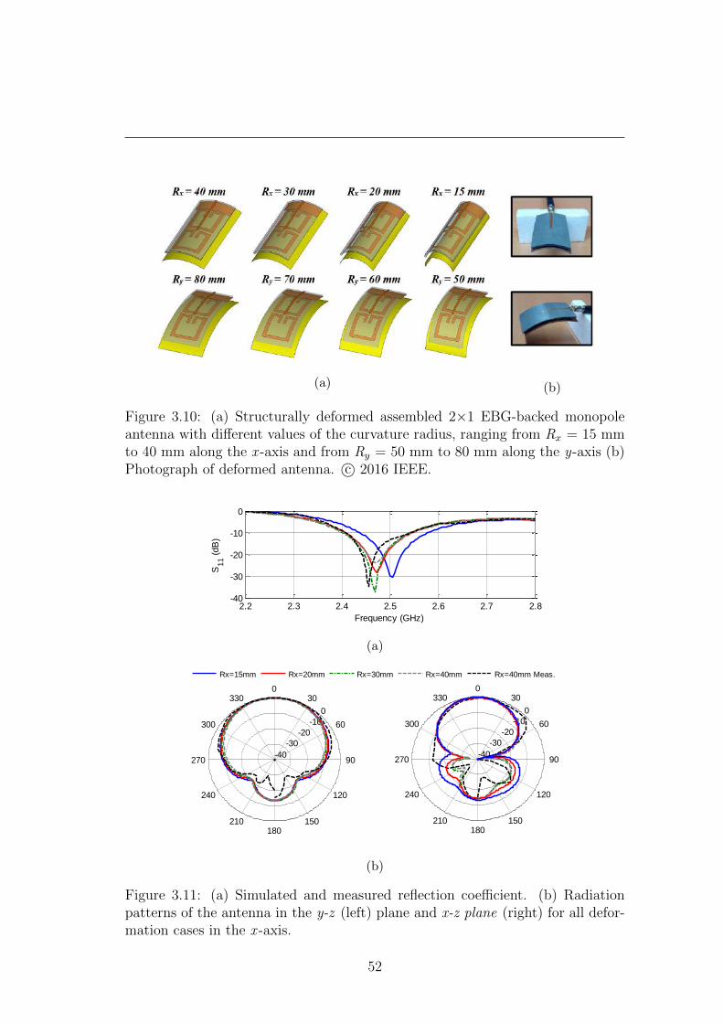
(a)
(b)
Figure 3.10: (a) Structurally deformed assembled 2×1 EBG-backed monopoleantenna with different values of the curvature radius, ranging from Rx = 15 mmto 40 mm along the x -axis and from Ry = 50 mm to 80 mm along the y-axis (b)Photograph of deformed antenna. c© 2016 IEEE.
2.2 2.3 2.4 2.5 2.6 2.7 2.8-40
-30
-20
-10
0
Frequency (GHz)
S11 (
dB
)
(a)
2.2 2.3 2.4 2.5 2.6 2.7 2.8-40
-35
-30
-25
-20
-15
-10
-5
0
Frequency (GHz)
S11 (
dB
)
Rx=15mm Rx=20mm Rx=30mm Rx=40mm Rx=40mm Meas.
0
-10
-20
-30
-40
030
60
90
120
150180
210
240
270
300
330
0
-10
-20
-30
-40
030
60
90
120
150180
210
240
270
300
330
(b)
Figure 3.11: (a) Simulated and measured reflection coefficient. (b) Radiationpatterns of the antenna in the y-z (left) plane and x-z plane (right) for all defor-mation cases in the x -axis.
52
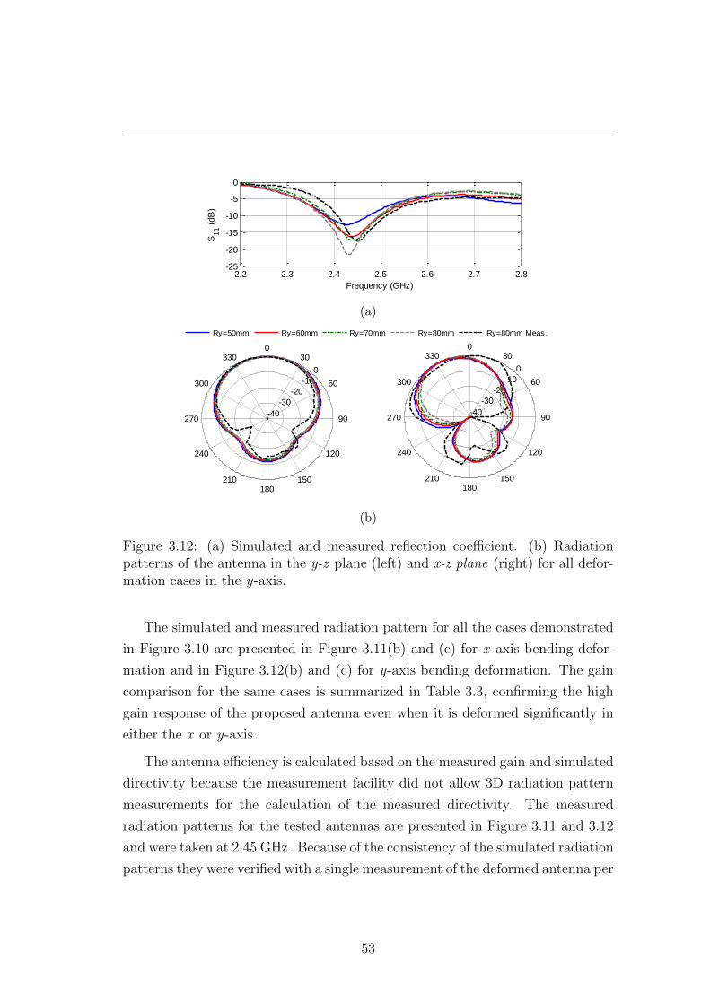
2.2 2.3 2.4 2.5 2.6 2.7 2.8-25
-20
-15
-10
-5
0
Frequency (GHz)
S11 (
dB
)
(a)
2.2 2.3 2.4 2.5 2.6 2.7 2.8-25
-20
-15
-10
-5
0
Frequency (GHz)
S11 (
dB
)
Ry=50mm Ry=60mm Ry=70mm Ry=80mm Ry=80mm Meas.
0
-10
-20
-30
-40
030
60
90
120
150180
210
240
270
300
330
0
-10
-20
-30
-40
030
60
90
120
150180
210
240
270
300
330
(b)
Figure 3.12: (a) Simulated and measured reflection coefficient. (b) Radiationpatterns of the antenna in the y-z plane (left) and x-z plane (right) for all defor-mation cases in the y-axis.
The simulated and measured radiation pattern for all the cases demonstrated
in Figure 3.10 are presented in Figure 3.11(b) and (c) for x -axis bending defor-
mation and in Figure 3.12(b) and (c) for y-axis bending deformation. The gain
comparison for the same cases is summarized in Table 3.3, confirming the high
gain response of the proposed antenna even when it is deformed significantly in
either the x or y-axis.
The antenna efficiency is calculated based on the measured gain and simulated
directivity because the measurement facility did not allow 3D radiation pattern
measurements for the calculation of the measured directivity. The measured
radiation patterns for the tested antennas are presented in Figure 3.11 and 3.12
and were taken at 2.45 GHz. Because of the consistency of the simulated radiation
patterns they were verified with a single measurement of the deformed antenna per
53
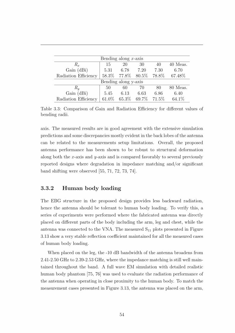
Bending along x -axisRx 15 20 30 40 40 Meas.
Gain (dBi) 5.31 6.78 7.20 7.30 6.70Radiation Efficiency 58.3% 77.8% 80.5% 78.8% 67.48%
Bending along y-axisRy 50 60 70 80 80 Meas.
Gain (dBi) 5.45 6.13 6.63 6.86 6.40Radiation Efficiency 61.0% 65.3% 69.7% 71.5% 64.1%
Table 3.3: Comparison of Gain and Radiation Efficiency for different values ofbending radii.
axis. The measured results are in good agreement with the extensive simulation
predictions and some discrepancies mostly evident in the back lobes of the antenna
can be related to the measurements setup limitations. Overall, the proposed
antenna performance has been shown to be robust to structural deformation
along both the x -axis and y-axis and is compared favorably to several previously
reported designs where degradation in impedance matching and/or significant
band shifting were observed [55, 71, 72, 73, 74].
3.3.2 Human body loading
The EBG structure in the proposed design provides less backward radiation,
hence the antenna should be tolerant to human body loading. To verify this, a
series of experiments were performed where the fabricated antenna was directly
placed on different parts of the body including the arm, leg and chest, while the
antenna was connected to the VNA. The measured S11 plots presented in Figure
3.13 show a very stable reflection coefficient maintained for all the measured cases
of human body loading.
When placed on the leg, the -10 dB bandwidth of the antenna broadens from
2.41-2.50 GHz to 2.39-2.53 GHz, where the impedance matching is still well main-
tained throughout the band. A full wave EM simulation with detailed realistic
human body phantom [75, 76] was used to evaluate the radiation performance of
the antenna when operating in close proximity to the human body. To match the
measurement cases presented in Figure 3.13, the antenna was placed on the arm,
54
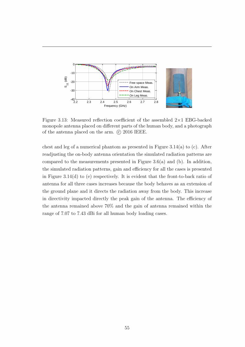
2.2 2.3 2.4 2.5 2.6 2.7 2.8-40
-30
-20
-10
0
Frequency (GHz)
S11 (
dB
)
Free space Meas.
On Arm Meas.
On Chest Meas.
On Leg Meas.
Figure 3.13: Measured reflection coefficient of the assembled 2×1 EBG-backedmonopole antenna placed on different parts of the human body, and a photographof the antenna placed on the arm. c© 2016 IEEE.
chest and leg of a numerical phantom as presented in Figure 3.14(a) to (c). After
readjusting the on-body antenna orientation the simulated radiation patterns are
compared to the measurements presented in Figure 3.6(a) and (b). In addition,
the simulated radiation patterns, gain and efficiency for all the cases is presented
in Figure 3.14(d) to (e) respectively. It is evident that the front-to-back ratio of
antenna for all three cases increases because the body behaves as an extension of
the ground plane and it directs the radiation away from the body. This increase
in directivity impacted directly the peak gain of the antenna. The efficiency of
the antenna remained above 70% and the gain of antenna remained within the
range of 7.07 to 7.43 dBi for all human body loading cases.
55
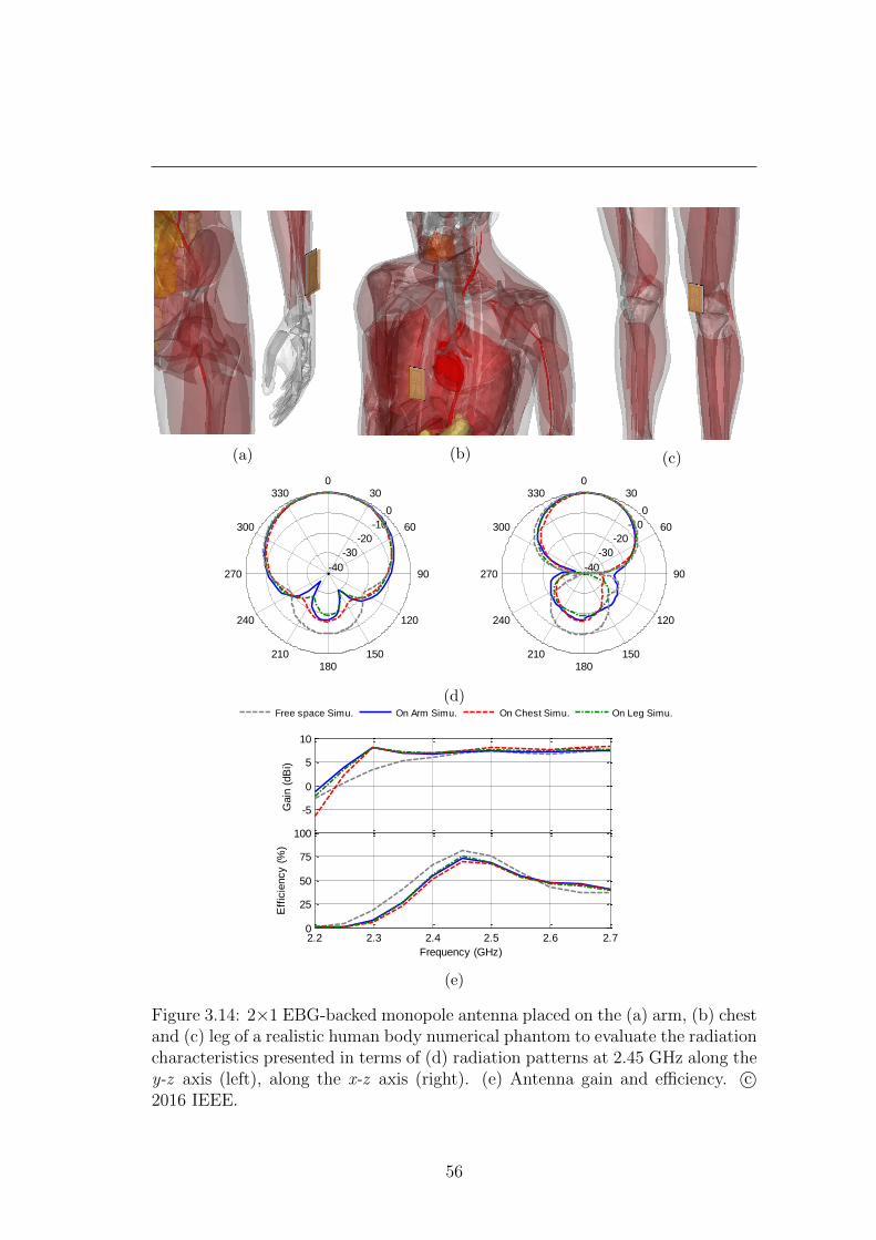
(a)
(b)
(c)
(d) (e)
(f)
0
-10
-20
-30
-40
030
60
90
120
150180
210
240
270
300
330
0
-10
-20
-30
-40
030
60
90
120
150180
210
240
270
300
330
2.2 2.3 2.4 2.5 2.6 2.7
-5
0
5
10
-5
0
5
10
Gain
(dB
i)
Frequency (GHz)
Free space Simu. On Arm Simu. On Chest Simu. On Leg Simu.
-5
0
5
10
Gain
(dB
i)
2.2 2.3 2.4 2.5 2.6 2.70
25
50
75
100
Frequency (GHz)
Eff
icie
ncy (
%)
(d)
(d) (e)
(f)
0
-10
-20
-30
-40
030
60
90
120
150180
210
240
270
300
330
0
-10
-20
-30
-40
030
60
90
120
150180
210
240
270
300
330
2.2 2.3 2.4 2.5 2.6 2.7
-5
0
5
10
-5
0
5
10
Gain
(dB
i)
Frequency (GHz)
Free space Simu. On Arm Simu. On Chest Simu. On Leg Simu.
-5
0
5
10
Gain
(dB
i)
2.2 2.3 2.4 2.5 2.6 2.70
25
50
75
100
Frequency (GHz)
Eff
icie
ncy (
%)
(e)
Figure 3.14: 2×1 EBG-backed monopole antenna placed on the (a) arm, (b) chestand (c) leg of a realistic human body numerical phantom to evaluate the radiationcharacteristics presented in terms of (d) radiation patterns at 2.45 GHz along they-z axis (left), along the x-z axis (right). (e) Antenna gain and efficiency. c©2016 IEEE.
56
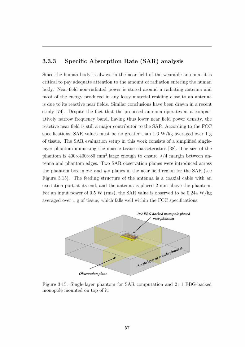
3.3.3 Specific Absorption Rate (SAR) analysis
Since the human body is always in the near-field of the wearable antenna, it is
critical to pay adequate attention to the amount of radiation entering the human
body. Near-field non-radiated power is stored around a radiating antenna and
most of the energy produced in any lossy material residing close to an antenna
is due to its reactive near fields. Similar conclusions have been drawn in a recent
study [74]. Despite the fact that the proposed antenna operates at a compar-
atively narrow frequency band, having thus lower near field power density, the
reactive near field is still a major contributor to the SAR. According to the FCC
specifications, SAR values must be no greater than 1.6 W/kg averaged over 1 g
of tissue. The SAR evaluation setup in this work consists of a simplified single-
layer phantom mimicking the muscle tissue characteristics [38]. The size of the
phantom is 400×400×80 mm3,large enough to ensure λ/4 margin between an-
tenna and phantom edges. Two SAR observation planes were introduced across
the phantom box in x-z and y-z planes in the near field region for the SAR (see
Figure 3.15). The feeding structure of the antenna is a coaxial cable with an
excitation port at its end, and the antenna is placed 2 mm above the phantom.
For an input power of 0.5 W (rms), the SAR value is observed to be 0.244 W/kg
averaged over 1 g of tissue, which falls well within the FCC specifications.
Figure 3.15: Single-layer phantom for SAR computation and 2×1 EBG-backedmonopole mounted on top of it.
57
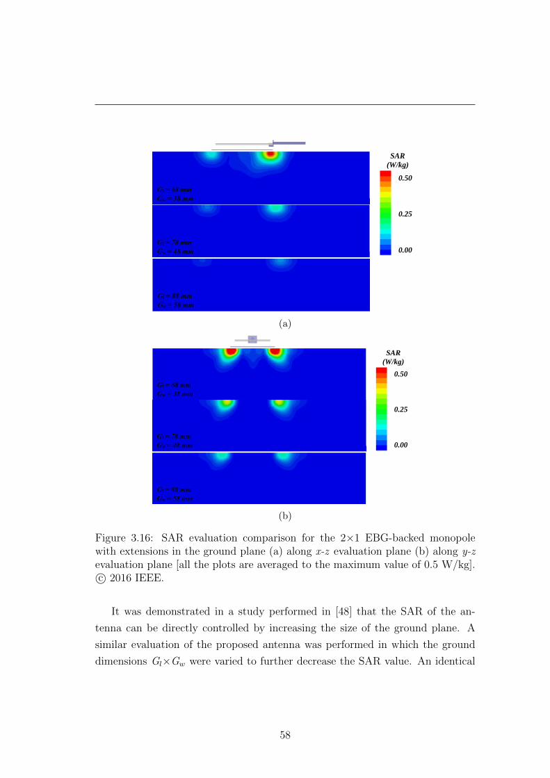
SAR
(W/kg)
0.50
0.25
0.00
(a)
SAR
(W/kg)
0.50
0.25
0.00
(b)
Figure 3.16: SAR evaluation comparison for the 2×1 EBG-backed monopolewith extensions in the ground plane (a) along x-z evaluation plane (b) along y-zevaluation plane [all the plots are averaged to the maximum value of 0.5 W/kg].c© 2016 IEEE.
It was demonstrated in a study performed in [48] that the SAR of the an-
tenna can be directly controlled by increasing the size of the ground plane. A
similar evaluation of the proposed antenna was performed in which the ground
dimensions Gl×Gw were varied to further decrease the SAR value. An identical
58
environment in terms of operating frequency, phantom size, phantom structure,
feeding, and position of the antenna was used and the SAR was estimated over the
observation planes shown in Figure 3.16. When the ground dimensions Gl×Gw
were increased from 68×38 mm2 to 78×48 mm2 (144%) and 88×58 mm2(197%)
respectively, while keeping all other parameters constant, a significant drop in
SAR was observed, as can be witnessed from the 2D plots on the observation
planes shown in Figure 3.16 (a) and (b). Note that all observation planes are
uniformly color coded from 0 to 0.5 W/kg. It was discussed previously in sec-
tions I and II how the grounded EBG plane directs the radiation of the antenna
towards the positive z -axis, however some of the diffracted fields from the edges
of the ground plane were still seen to radiate towards the body. This effect can be
controlled by increasing further the dimensions of the ground plane, giving an ad-
ditional control parameter to the proposed antenna over the SAR. In conclusion,
whenever it is possible, and allowed by the application, the size of the ground
plane backing the EBG should be increased to further decrease the maximum
SAR.
3.4 Chapter Conclusions
A compact semi-flexible 2×1 EBG-backed planar monopole antenna for wearable
applications has been proposed and tested experimentally. The proposed an-
tenna exhibits very good size and gain characteristics compared to most recently
reported configurations listed in Table 3.4, which are intended for wearable ap-
plications. The EBG array in the proposed structure not only serves to isolate
the antenna from the human body, but also contributes towards enhanced radi-
ation efficiency. The fabricated antenna performs in good agreement with the
simulated structure. It has a 4.8%, −10 dB, fractional bandwidth at the ISM
band and a measured gain of 6.88 dBi, far greater than the gain of a conventional
planar monopole antenna. The measured radiation pattern characteristics have
been qualitatively explained using an eight-element array model consisting of six
magnetic current sources and two electric current sources. Full-wave simulations
and experimental measurements further revealed the robustness of the antenna
59
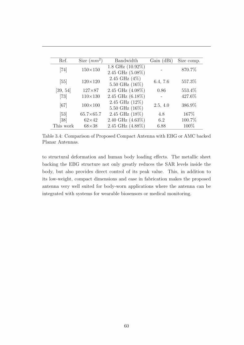
Ref. Size (mm2) Bandwidth Gain (dBi) Size comp.
[74] 150×1501.8 GHz (10.92%)2.45 GHz (5.08%)
- 870.7%
[55] 120×1202.45 GHz (4%)5.50 GHz (16%)
6.4, 7.6 557.3%
[39, 54] 127×87 2.45 GHz (4.08%) 0.86 553.4%[73] 110×130 2.45 GHz (6.18%) - 427.6%
[67] 100×1002.45 GHz (12%)5.50 GHz (16%)
2.5, 4.0 386.9%
[53] 65.7×65.7 2.45 GHz (18%) 4.8 167%[38] 62×42 2.40 GHz (4.63%) 6.2 100.7%
This work 68×38 2.45 GHz (4.88%) 6.88 100%
Table 3.4: Comparison of Proposed Compact Antenna with EBG or AMC backedPlanar Antennas.
to structural deformation and human body loading effects. The metallic sheet
backing the EBG structure not only greatly reduces the SAR levels inside the
body, but also provides direct control of its peak value. This, in addition to
its low-weight, compact dimensions and ease in fabrication makes the proposed
antenna very well suited for body-worn applications where the antenna can be
integrated with systems for wearable biosensors or medical monitoring.
60
Chapter 4
Electrically Small Implantable
Antenna
This work discusses the design method towards the implementation of a com-
pact, stacked, implantable antenna for biotelemetry applications. The proposed
antenna consists of three stacked layers, printed on high permittivity grounded
substrate. The bottom layer of the antenna above the ground plane, contains
a meandered structure with a symmetrically placed T-shaped slot. The middle
layer consists of two U-shaped radiators and an M-shaped metallic segment is
further added on the top layer to further enhance the radiation efficiency of the
antenna. These three stacked layers, form a symmetrical closed loop structure
resonating on its fundamental resonant mode, at 403 MHz, for the Medical Im-
plant Communication Service (MICS) band. A shifted higher order mode of the
same closed loop structure, along with the negative currents on ground plane en-
ables wide band operation, at 2.45 GHz, for the industrial, scientific, and medical
(ISM) band. To resolve the constraints associated with implanting an antenna
in human body that usually results in detuning and impedance mismatch, the
antennas most important radiating sections were thoroughly investigated. A fully
parametrized solution is proposed that makes the antenna a good candidate for
a device, implanted at several different areas of the human body with potentially
different electrical properties with consequently different detuning effect. For fur-
ther investigation, the particle swarm algorithm was implemented to optimize the
61
antennas performance while operating inside a compact, 23x23x5mm3 block of
human skin, equivalent phantom. The simulated performance of the proposed
prototype antenna, indicates that it can be used for either in-vitro or in-vivo
operations. Any wireless communication between implantable antenna and an
external off-body antenna suffers significant link loss due to the lossy nature of
living human tissues. This link degradation is normally unpredictable and varies
for different parts of the human body. To study an implantable communication
scenario, complete setup is generally simulated using a full wave electromag-
netic simulator. Such simulation requires human body phantoms having electri-
cal properties such as permittivity and bulk conductivity, or even mass density
similar to that of real body tissues. It has been observed that geometry of such
phantoms is usually chosen as simple as possible to decrease the required compu-
tational resources and the overall time for the completion of the simulation. It is
difficult to predict how much error is expected when realistic phantom is replaced
by such geometrically simpler phantom. This study focuses on a comparison of
the usefulness of using realistic human body phantoms over geometrically simple
body phantoms for through-body communication simulation. To study this com-
parison, an implantable antenna, placed inside a human stomach model, is set
to communicate with an off-body antenna at Medical Implant Communication
Service (MICS) band. Keeping the distance between implantable antenna and
off-body antenna constant, the realistic human body phantom is then replaced
by two types of layered body phantoms with different complexity. Results in
the form of calculated s-parameters and phantom complexity metrics are further
investigated to conclude the study.
4.1 Design Challenges
Biotelemetry enables full duplex wireless communication between implantable
antennas with on-body receiver antennas. Designing a wearable on-body antenna
is comparatively easier because of its placement in an environment where body
is normally in one direction and air in the other. This, allows the designers
to control the radiation pattern of the antenna towards the human body by
62
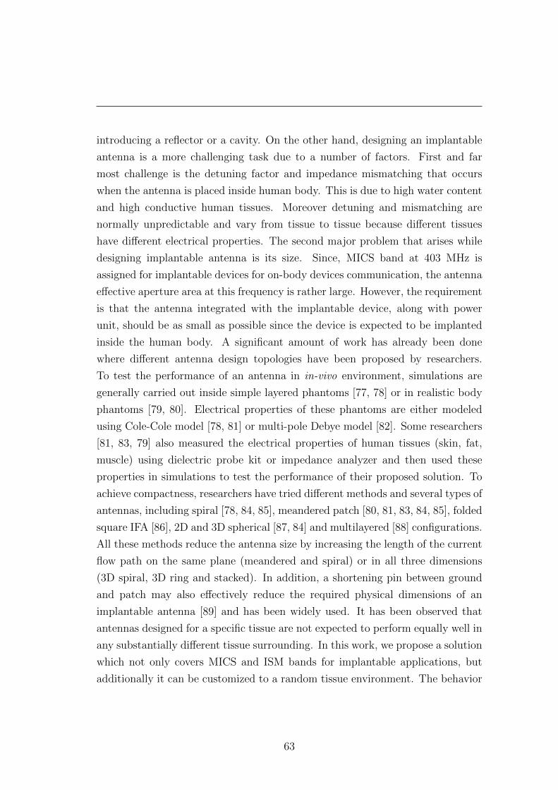
introducing a reflector or a cavity. On the other hand, designing an implantable
antenna is a more challenging task due to a number of factors. First and far
most challenge is the detuning factor and impedance mismatching that occurs
when the antenna is placed inside human body. This is due to high water content
and high conductive human tissues. Moreover detuning and mismatching are
normally unpredictable and vary from tissue to tissue because different tissues
have different electrical properties. The second major problem that arises while
designing implantable antenna is its size. Since, MICS band at 403 MHz is
assigned for implantable devices for on-body devices communication, the antenna
effective aperture area at this frequency is rather large. However, the requirement
is that the antenna integrated with the implantable device, along with power
unit, should be as small as possible since the device is expected to be implanted
inside the human body. A significant amount of work has already been done
where different antenna design topologies have been proposed by researchers.
To test the performance of an antenna in in-vivo environment, simulations are
generally carried out inside simple layered phantoms [77, 78] or in realistic body
phantoms [79, 80]. Electrical properties of these phantoms are either modeled
using Cole-Cole model [78, 81] or multi-pole Debye model [82]. Some researchers
[81, 83, 79] also measured the electrical properties of human tissues (skin, fat,
muscle) using dielectric probe kit or impedance analyzer and then used these
properties in simulations to test the performance of their proposed solution. To
achieve compactness, researchers have tried different methods and several types of
antennas, including spiral [78, 84, 85], meandered patch [80, 81, 83, 84, 85], folded
square IFA [86], 2D and 3D spherical [87, 84] and multilayered [88] configurations.
All these methods reduce the antenna size by increasing the length of the current
flow path on the same plane (meandered and spiral) or in all three dimensions
(3D spiral, 3D ring and stacked). In addition, a shortening pin between ground
and patch may also effectively reduce the required physical dimensions of an
implantable antenna [89] and has been widely used. It has been observed that
antennas designed for a specific tissue are not expected to perform equally well in
any substantially different tissue surrounding. In this work, we propose a solution
which not only covers MICS and ISM bands for implantable applications, but
additionally it can be customized to a random tissue environment. The behavior
63
of the antenna is thoroughly studied and a range of geometric parameters are
presented for best antenna performance.
Figure 4.1: The geometry of proposed Implantable antenna. with lsub = 15mm,hsub = 0.635mm, wsub = 18mm, hcoat = 17µm, l = 13.8mm and w = 16.56mm.c© 2015 PIERS
4.2 Multi-layered Implantable Antenna
Figure 4.1 shows the geometry of the proposed layered implantable antenna. The
overall dimensions of the antenna are 15x18x1.97mm3, and the antenna consists of
three copper coated substrate layers. In this study, Roger’s RO3210 as substrate
was used since its electrical properties resemble with those of biocompatible sub-
strate ceramic alumina (εr=9.4 and tanδ=0.006). RO3210 was preferred because
it can be easily available and is compatible with conventional fabrication tech-
niques making in-house prototype fabrication possible. The proposed antenna
consists of the ground layer and three stacked patch layers as shown in Figure 4.1
The bottom layer of the antenna, fed at the upper right corner, comprises a patch
with identical slits having length and width pl1, pl3, pw1 and pw3 respectively.
These slots along with the T shaped slot in the middle of the patch introduce a
meandered structure used for size reduction. To further decrease the size of the
64
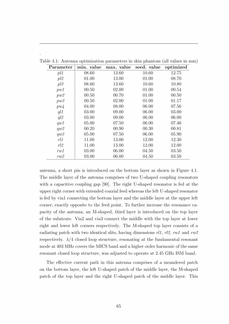
.
Table 4.1: Antenna optimization parameters in skin phantom (all values in mm)
Parameter min. value max. value seed. value optimizedpl1 08.60 13.60 10.60 12.75pl2 01.00 13.00 01.00 08.70pl3 08.60 13.60 10.60 10.80pw1 00.50 02.00 01.00 00.54pw2 00.50 00.70 01.00 00.50pw3 00.50 02.00 01.00 01.17pw4 04.00 08.00 06.00 07.56ql1 03.00 09.00 06.00 03.00ql2 03.00 09.00 06.00 06.00qw1 05.00 07.50 06.00 07.46qw2 00.20 00.90 00.30 00.81qw3 05.00 07.50 06.00 05.90rl1 11.00 13.00 12.00 12.30rl2 11.00 13.00 12.00 12.00rw1 03.00 06.00 04.50 03.50rw2 03.00 06.00 04.50 03.50
antenna, a short pin is introduced on the bottom layer as shown in Figure 4.1.
The middle layer of the antenna comprises of two U-shaped coupling resonators
with a capacitive coupling gap [90]. The right U-shaped resonator is fed at the
upper right corner with extended coaxial feed whereas the left U-shaped resonator
is fed by via1 connecting the bottom layer and the middle layer at the upper left
corner, exactly opposite to the feed point. To further increase the resonance ca-
pacity of the antenna, an M-shaped, third layer is introduced on the top layer
of the substrate. Via2 and via3 connect the middle with the top layer at lower
right and lower left corners respectively. The M-shaped top layer consists of a
radiating patch with two identical slits, having dimensions rl1, rl2, rw1 and rw2
respectively. λ/4 closed loop structure, resonating at the fundamental resonant
mode at 403 MHz covers the MICS band and a higher order harmonic of the same
resonant closed loop structure, was adjusted to operate at 2.45 GHz ISM band.
The effective current path in this antenna comprises of a meandered patch
on the bottom layer, the left U-shaped patch of the middle layer, the M-shaped
patch of the top layer and the right U-shaped patch of the middle layer. This
65
current path makes an approximately λ/4 closed loop structure, resonating at
the fundamental resonant mode at 403 MHz covering the MICS band. Further-
more, a higher order harmonic of the same resonant closed loop structure, was
adjusted to operate at 2.45 GHz ISM band, resulting in a dual band operation
using the same structure. To further enhance the radiation efficiency of the pro-
posed antenna at ISM band, the effective length of the meandered patch on the
bottom layer, that depends upon its coupling with the ground plane was further
optimized. The next step was to study the behavior of the antenna in different
tissue surroundings, which is equivalent to implanting the antenna at different
body parts, and to identify various antenna tuning parameters simultaneously,
for MICS and ISM bands. This study resulted in a fully parametrized antenna
model with a minimum and maximum defined range of geometrical parameters
that may adjust the effective wavelength of the λ/4 closed loop resonator, and
the meandered patch of the bottom layer. One case is presented in this paper
where the antenna is placed in 23x23x5 mm3 block of human skin phantom. Note
that measured electrical properties of skin tissue reported in [81], were used for
this test. As predicted, significant detuning was observed both at MICS and ISM
bands as shown in Figure 4.2a.
Results shown in Figure 4.2 (a), indicate that, when the antenna was placed
in skin phantom, a resonant frequency shift of around 50 MHz towards lower fre-
quencies, was observed for the MICS band. Significant degradation in impedance
matching can also be observed in Figure 4.2 (a). The frequency downshift was
raised up to 130 MHz at the ISM band as can be seen in Figure 4.2 (b). In
order to tune the antenna dimensions on both targeted frequency bands simul-
taneously, particle swarm algorithm in combination with FDTD simulation was
used. The resulting set of optimized values of the antenna parameters are listed
in the fourth column of Table 1, where the third column shows the seed values
for the particle swarm optimizer. The watch function to optimize the antenna in
given tissue environment is set to be:
f = max(|S11(dB)403MHz|, |S11(dB)2.45GHz|) (4.1)
It took 20 iterations for the particle swarm algorithm to converge and tune
66
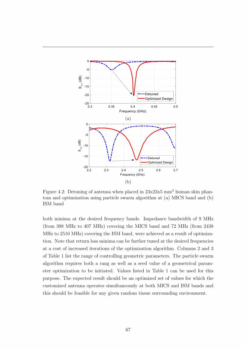
(a)
(b)
Figure 4.2: Detuning of antenna when placed in 23x23x5 mm3 human skin phan-tom and optimization using particle swarm algorithm at (a) MICS band and (b)ISM band
both minima at the desired frequency bands. Impedance bandwidth of 9 MHz
(from 398 MHz to 407 MHz) covering the MICS band and 72 MHz (from 2438
MHz to 2510 MHz) covering the ISM band, were achieved as a result of optimiza-
tion. Note that return loss minima can be further tuned at the desired frequencies
at a cost of increased iterations of the optimization algorithm. Columns 2 and 3
of Table 1 list the range of controlling geometric parameters. The particle swarm
algorithm requires both a rang as well as a seed value of a geometrical param-
eter optimization to be initiated. Values listed in Table 1 can be used for this
purpose. The expected result should be an optimized set of values for which the
customized antenna operates simultaneously at both MICS and ISM bands and
this should be feasible for any given random tissue surrounding environment.
67
4.3 Numerical Phantom Selection for Implant
Study
Implantable devices for biomedical applications play vital role in building com-
prehensive telemedicine wireless communication networks. Before an implantable
device is proposed, it is usually thoroughly simulated at system level, using nu-
merical methods in order to study the electromagnetic propagation loss when
the DUT is placed inside human body. Computerized MRI scanner deduced,
detailed body phantoms are finding increasingly important role in the attempt
to test the performance of such implantable devices on system level. A number
of 3D phantoms, deduced from MRI scans of living subjects [91, 92], depicting
indirectly measured electrical properties of human tissues, are widely used, for
case to case based, implantable device, design problems. These models generally
have frequency-dependent electrical properties, and they are similar in shape to
realistic human body parts and thus geometrically complex. Example of such
complex phantoms for medical imaging and implantable applications are pre-
sented in [93]. Alternatively another simpler approach is widely used, where
dense material blocks or homogeneous layers with constant electrical properties
similar to those of predominant human tissues are built and used in EM sim-
ulations for implantable devices problems [94, 95]. These mainly homogeneous
blocks, consist of simple geometric shapes which result in low mesh complexity,
during modeling in 3D CAD tools, and are therefore far less resources hungry
when simulated using full wave EM solvers. The main problem limiting the use
of layered homogeneous models, is related to their accuracy and consequently
their reliability. This study aims to assess the reliability of such simpler mod-
els in comparison with the more complex structures of realistic body-mimicking
models. Towards this end, a theoretical scenario is discussed through extensive
simulations, in which the communication between an implantable device, located
inside a human stomach model, and an off-body device placed near the abdomen
is investigated. A novel, compact, multilayered, implantable antenna, operat-
ing at 403 MHz, is used to establish a through-body communication scenario
with a near-body transceivers antenna. Keeping in mind the detuning effect of
68
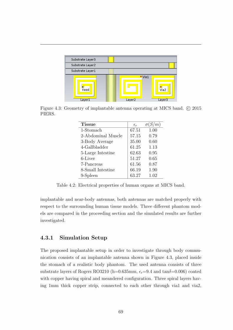
Figure 4.3: Geometry of implantable antenna operating at MICS band. c© 2015PIERS.
Tissue εr σ(S/m)1-Stomach 67.51 1.002-Abdominal Muscle 57.15 0.793-Body Average 35.00 0.604-Gallbladder 61.25 1.135-Large Intestine 62.63 0.956-Liver 51.27 0.657-Pancreas 61.56 0.878-Small Intestine 66.19 1.909-Spleen 63.27 1.02
Table 4.2: Electrical properties of human organs at MICS band.
implantable and near-body antennas, both antennas are matched properly with
respect to the surrounding human tissue models. Three different phantom mod-
els are compared in the proceeding section and the simulated results are further
investigated.
4.3.1 Simulation Setup
The proposed implantable setup in order to investigate through body commu-
nication consists of an implantable antenna shown in Figure 4.3, placed inside
the stomach of a realistic body phantom. The used antenna consists of three
substrate layers of Rogers RO3210 (h=0.635mm, εr=9.4 and tanδ=0.006) coated
with copper having spiral and meandered configuration. Three spiral layers hav-
ing 1mm thick copper strip, connected to each other through via1 and via2,
69
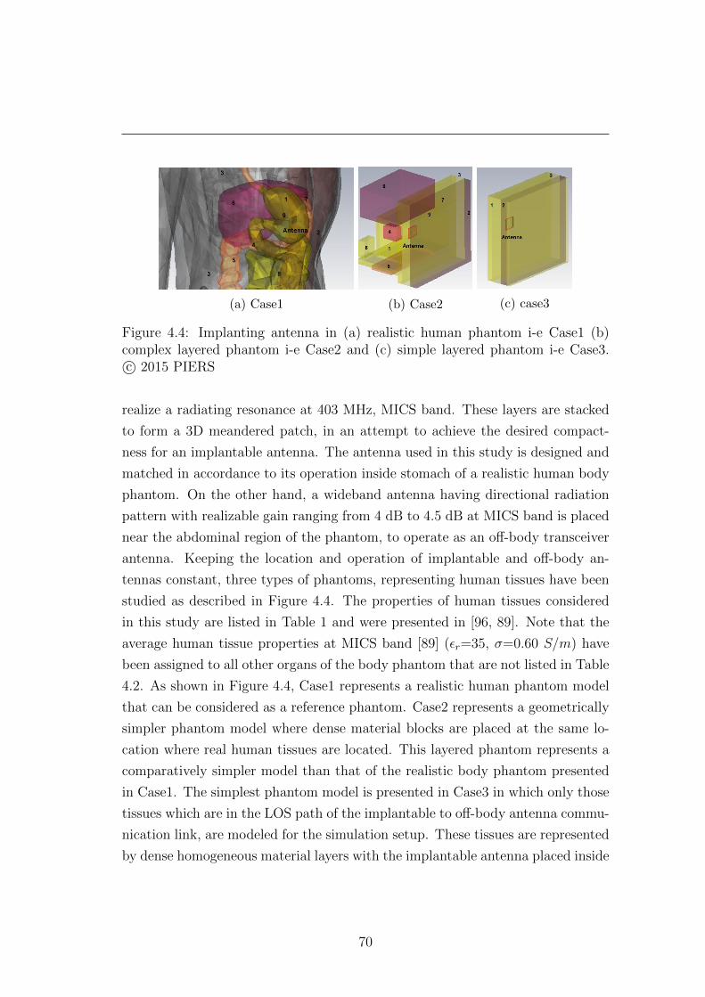
(a) Case1 (b) Case2 (c) case3
Figure 4.4: Implanting antenna in (a) realistic human phantom i-e Case1 (b)complex layered phantom i-e Case2 and (c) simple layered phantom i-e Case3.c© 2015 PIERS
realize a radiating resonance at 403 MHz, MICS band. These layers are stacked
to form a 3D meandered patch, in an attempt to achieve the desired compact-
ness for an implantable antenna. The antenna used in this study is designed and
matched in accordance to its operation inside stomach of a realistic human body
phantom. On the other hand, a wideband antenna having directional radiation
pattern with realizable gain ranging from 4 dB to 4.5 dB at MICS band is placed
near the abdominal region of the phantom, to operate as an off-body transceiver
antenna. Keeping the location and operation of implantable and off-body an-
tennas constant, three types of phantoms, representing human tissues have been
studied as described in Figure 4.4. The properties of human tissues considered
in this study are listed in Table 1 and were presented in [96, 89]. Note that the
average human tissue properties at MICS band [89] (εr=35, σ=0.60 S/m) have
been assigned to all other organs of the body phantom that are not listed in Table
4.2. As shown in Figure 4.4, Case1 represents a realistic human phantom model
that can be considered as a reference phantom. Case2 represents a geometrically
simpler phantom model where dense material blocks are placed at the same lo-
cation where real human tissues are located. This layered phantom represents a
comparatively simpler model than that of the realistic body phantom presented
in Case1. The simplest phantom model is presented in Case3 in which only those
tissues which are in the LOS path of the implantable to off-body antenna commu-
nication link, are modeled for the simulation setup. These tissues are represented
by dense homogeneous material layers with the implantable antenna placed inside
70
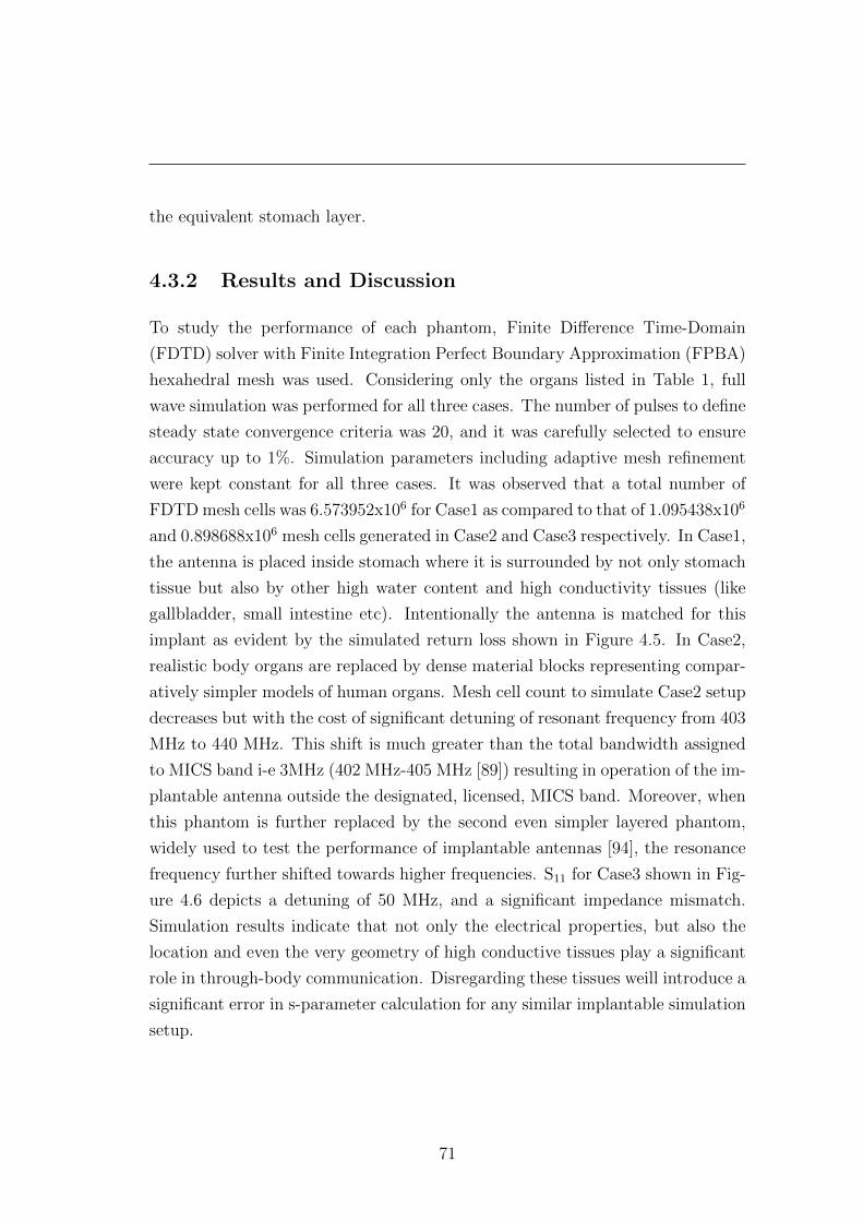
the equivalent stomach layer.
4.3.2 Results and Discussion
To study the performance of each phantom, Finite Difference Time-Domain
(FDTD) solver with Finite Integration Perfect Boundary Approximation (FPBA)
hexahedral mesh was used. Considering only the organs listed in Table 1, full
wave simulation was performed for all three cases. The number of pulses to define
steady state convergence criteria was 20, and it was carefully selected to ensure
accuracy up to 1%. Simulation parameters including adaptive mesh refinement
were kept constant for all three cases. It was observed that a total number of
FDTD mesh cells was 6.573952x10⁶ for Case1 as compared to that of 1.095438x10⁶
and 0.898688x10⁶ mesh cells generated in Case2 and Case3 respectively. In Case1,
the antenna is placed inside stomach where it is surrounded by not only stomach
tissue but also by other high water content and high conductivity tissues (like
gallbladder, small intestine etc). Intentionally the antenna is matched for this
implant as evident by the simulated return loss shown in Figure 4.5. In Case2,
realistic body organs are replaced by dense material blocks representing compar-
atively simpler models of human organs. Mesh cell count to simulate Case2 setup
decreases but with the cost of significant detuning of resonant frequency from 403
MHz to 440 MHz. This shift is much greater than the total bandwidth assigned
to MICS band i-e 3MHz (402 MHz-405 MHz [89]) resulting in operation of the im-
plantable antenna outside the designated, licensed, MICS band. Moreover, when
this phantom is further replaced by the second even simpler layered phantom,
widely used to test the performance of implantable antennas [94], the resonance
frequency further shifted towards higher frequencies. S11 for Case3 shown in Fig-
ure 4.6 depicts a detuning of 50 MHz, and a significant impedance mismatch.
Simulation results indicate that not only the electrical properties, but also the
location and even the very geometry of high conductive tissues play a significant
role in through-body communication. Disregarding these tissues weill introduce a
significant error in s-parameter calculation for any similar implantable simulation
setup.
71
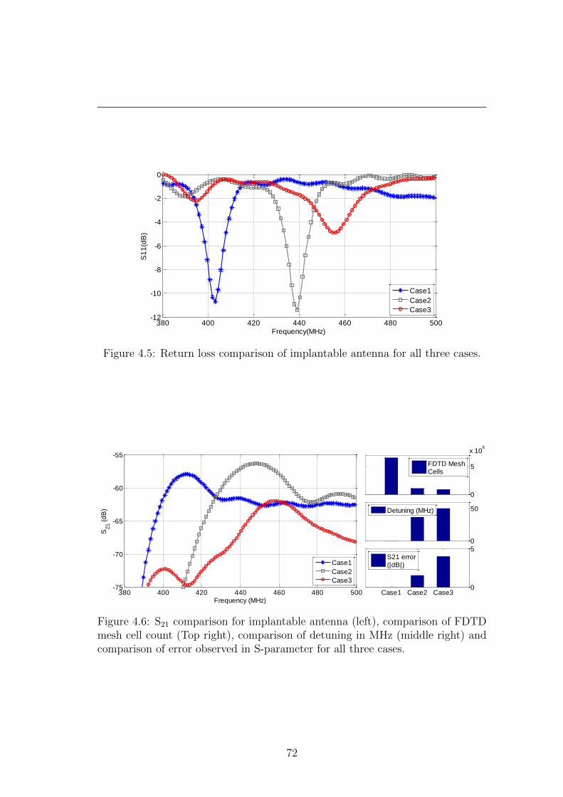
0
5
x 106
0
50
Case1 Case2 Case30
5
380 400 420 440 460 480 500-75
-70
-65
-60
-55
Frequency (MHz)
S21 (
dB
)
Case1
Case2
Case3
S21 error(|dB|)
Detuning (MHz)
FDTD MeshCells
380 400 420 440 460 480 500-12
-10
-8
-6
-4
-2
0
Frequency(MHz)
S1
1(d
B)
Case1
Case2
Case3
Figure 4.5: Return loss comparison of implantable antenna for all three cases.
0
5
x 106
0
50
Case1 Case2 Case30
5
380 400 420 440 460 480 500-75
-70
-65
-60
-55
Frequency (MHz)
S21 (
dB
)
Case1
Case2
Case3
S21 error(|dB|)
Detuning (MHz)
FDTD MeshCells
380 400 420 440 460 480 500-12
-10
-8
-6
-4
-2
0
Frequency(MHz)
S1
1(d
B)
Case1
Case2
Case3
Figure 4.6: S21 comparison for implantable antenna (left), comparison of FDTDmesh cell count (Top right), comparison of detuning in MHz (middle right) andcomparison of error observed in S-parameter for all three cases.
72
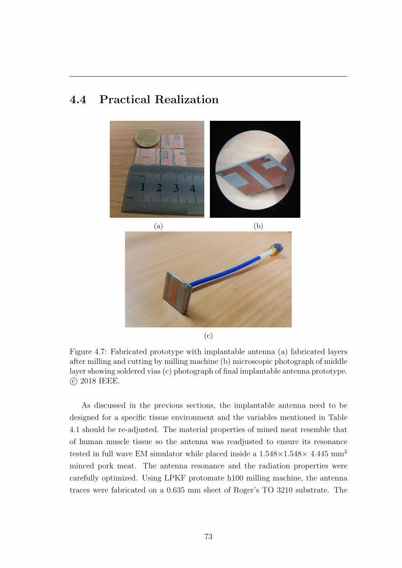
4.4 Practical Realization
(a) (b)
(c)
Figure 4.7: Fabricated prototype with implantable antenna (a) fabricated layersafter milling and cutting by milling machine (b) microscopic photograph of middlelayer showing soldered vias (c) photograph of final implantable antenna prototype.c© 2018 IEEE.
As discussed in the previous sections, the implantable antenna need to be
designed for a specific tissue environment and the variables mentioned in Table
4.1 should be re-adjusted. The material properties of mined meat resemble that
of human muscle tissue so the antenna was readjusted to ensure its resonance
tested in full wave EM simulator while placed inside a 1.548×1.548× 4.445 mm2
minced pork meat. The antenna resonance and the radiation properties were
carefully optimized. Using LPKF protomate h100 milling machine, the antenna
traces were fabricated on a 0.635 mm sheet of Roger’s TO 3210 substrate. The
73
substrate is very soft and need extra care to handle while placed inside the milling
machine. The process consisted of two major steps. First, the substrate sheet
was placed in vacuum suction panel of the machine and drill holes were created
for the via wires to pass through the substrate. In the next step, the excessive
copper was removed from the substrate in such a way that the milling routing
need not to go too deep, but scratch the copper evenly throughout the board.
The removal of the substraet sheet from the vacuum suction panel was done
without bending the antenna sheets. The antenna layers are presented in Figure
4.7(a) along with a size comparison. When the layers were ready, first, the via
wires of 0.35 mm radius were passed from the drilled holes. The wires were sold
at the top and bottom of each layer’s copper coating, while the bulges of the
solder were squeezed manually to ensure they stay at the same level with the
layer. Figure 4.7(b) shows the microscopic picture taken in a prospective view
to show the accuracy of the soldering and leveling of via wires. A low loss and
highly shielded coax cable from Amphenol RF R© (Model: 523-095-902-451-005
and Manufacturing Part: 095-902-451-005) was used to feed the antenna. The
choice of the cable was made keeping in mind the leaky wave and standing wave
possibility since the antenna ground plane is electrically small. When they layers
were stacked together, a few drops of low loss epoxy (super glue) were used to
stick from each other. A very careful taping of the entire implantable antenna
was done and the final fabricated antenna is shown in Figure 4.7(c).
4.4.1 Measurements within Tissue
Initial antenna testing were done by directly connecting it to the VNA and placing
it in the hand just to test that the whole fabrication process goes well. In the next
step, minced pork meat placed in a plastic container (εr is roughly equal to 1.5).
Since the εr of the antenna substrate is much higher and the distance between
the boundary of container is higher compared to the antenna size, the thin plastic
container with low εr was not taken into consideration while simulations. The
antenna was carefully placed in the middle half, and the was fully covered with
minced meat to form a block where the antenna is approximately in the middle.
The cable connecting the antenna to the VNA was carefully attached to a stand
74
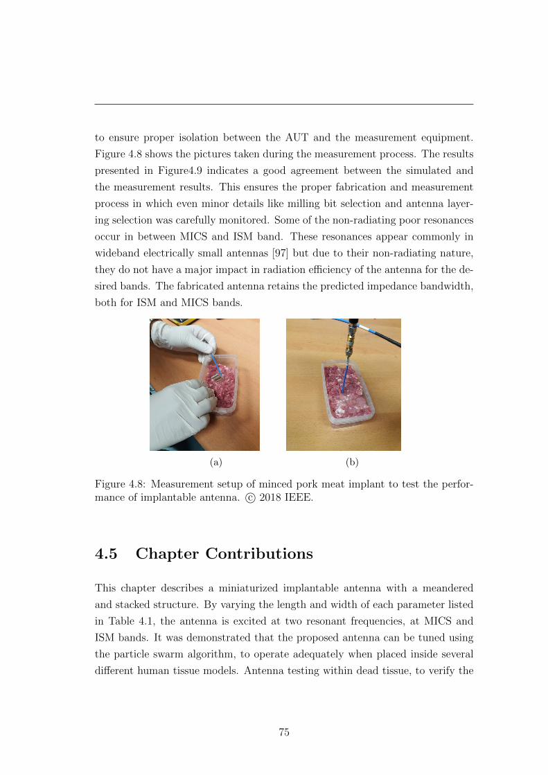
to ensure proper isolation between the AUT and the measurement equipment.
Figure 4.8 shows the pictures taken during the measurement process. The results
presented in Figure4.9 indicates a good agreement between the simulated and
the measurement results. This ensures the proper fabrication and measurement
process in which even minor details like milling bit selection and antenna layer-
ing selection was carefully monitored. Some of the non-radiating poor resonances
occur in between MICS and ISM band. These resonances appear commonly in
wideband electrically small antennas [97] but due to their non-radiating nature,
they do not have a major impact in radiation efficiency of the antenna for the de-
sired bands. The fabricated antenna retains the predicted impedance bandwidth,
both for ISM and MICS bands.
(a) (b)
Figure 4.8: Measurement setup of minced pork meat implant to test the perfor-mance of implantable antenna. c© 2018 IEEE.
4.5 Chapter Contributions
This chapter describes a miniaturized implantable antenna with a meandered
and stacked structure. By varying the length and width of each parameter listed
in Table 4.1, the antenna is excited at two resonant frequencies, at MICS and
ISM bands. It was demonstrated that the proposed antenna can be tuned using
the particle swarm algorithm, to operate adequately when placed inside several
different human tissue models. Antenna testing within dead tissue, to verify the
75
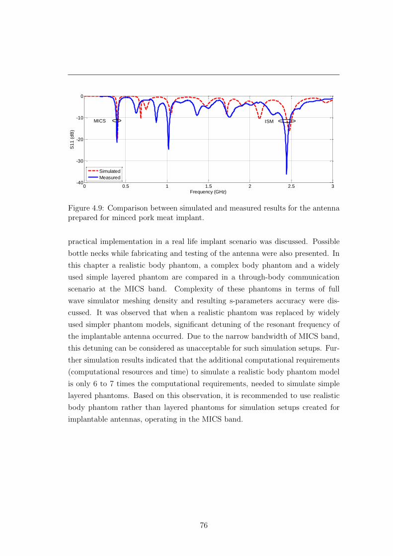
2.2 2.3 2.4 2.5 2.6 2.7-20
-15
-10
-5
0
Frequency (GHz)
S11 (
dB
)
Detuned
Optimized Design
2.2 2.3 2.4 2.5 2.6 2.7-20
-15
-10
-5
0
Frequency (GHz)
S11 (
dB
)
Detuned
Optimized Design
0 0.5 1 1.5 2 2.5 3-40
-30
-20
-10
0
Frequency (GHz)S
11
(d
B)
Simulated
Measured
ISMMICS
0 0.5 1 1.5 2 2.5 3-40
-30
-20
-10
0
Frequency (GHz)
S1
1 (
dB
)
Simulated
Measured
ISMMICS
Figure 4.9: Comparison between simulated and measured results for the antennaprepared for minced pork meat implant.
practical implementation in a real life implant scenario was discussed. Possible
bottle necks while fabricating and testing of the antenna were also presented. In
this chapter a realistic body phantom, a complex body phantom and a widely
used simple layered phantom are compared in a through-body communication
scenario at the MICS band. Complexity of these phantoms in terms of full
wave simulator meshing density and resulting s-parameters accuracy were dis-
cussed. It was observed that when a realistic phantom was replaced by widely
used simpler phantom models, significant detuning of the resonant frequency of
the implantable antenna occurred. Due to the narrow bandwidth of MICS band,
this detuning can be considered as unacceptable for such simulation setups. Fur-
ther simulation results indicated that the additional computational requirements
(computational resources and time) to simulate a realistic body phantom model
is only 6 to 7 times the computational requirements, needed to simulate simple
layered phantoms. Based on this observation, it is recommended to use realistic
body phantom rather than layered phantoms for simulation setups created for
implantable antennas, operating in the MICS band.
76

Chapter 5
Through- and across-body
communication
In health care sector, a reliable connectivity between the Body Centric Wireless
Communication (BCWC) sensor nodes is vital to patient’s health monitoring.
Investigation in the previous chapters revealed that the radiators for wearable
and implantable nodes need to work efficiently even in the presence of human
body. For a wearable antenna maintaining an off-body communication, high
directivity in the direction away from the body is the most important factors
as discussed in Chapter 3. To achieve this goal, a real or virtual isolation from
human body is preferable, which reduces the detuning and mismatching factor
due to body. For an implantable antennas, the directivity is of a secondary
importance, while the matching when an antenna is covered in a given tissue is
vital as discussed in Chapter 4. For a wearable sensor antenna intended for an
efficient communication with an implantable antenna or another node present on
any part of the body, both, the directivity as well as impedance miss-matching
need equal consideration. In this chapter, a wearable antenna for BCWC sensor
node (referred to in this chapter as wearable sensor antenna) is discussed, designed
to work reliably for a communication with an implantable. This completes the
link between body implant and off-body receiver, communicating with each other
via wearable node. Moreover, the connectivity between multiple wearable antenna
nodes placed around human body is discussed in the light of creeping-wave theory.
77
5.1 Introduction
With ongoing population growth and the associated rising health concerns, the
idea of transforming wired medical facilities into wireless biomedical sensors has
been increasingly studied in recent years. For an implantable sensor, physiological
variables such as glucose, oxygen and pH levels, and device parameters such as
battery life and mode of operation are considered to be essential readings. When
a patient is in critical condition in intensive care, these variables are required
to be monitored either continuously, or at very frequent intervals. The biggest
challenge in ensuring a stable wireless communication between an implantable
sensor and an on/off-body sensor lies in the fact that the RF signal needs to
propagate through the body. The impedance boundaries of the biological tissues
and the electromagnetic wave absorption result in a significant reduction of sig-
nal integrity. Furthermore, the performance of a newly designed sensor antenna
is difficult to be predicted in real life conditions due to the complicated hetero-
geneous time-changing electrical properties of the living tissues. Some studies
have shown experimental results of implantable antennas placed in either rat
skin [98, 81, 83], pork meat [99, 100], or skin-mimicking material [101] commu-
nicating with an external antenna. Recently, successful communication between
an implantable antenna and a smart phone has been shown in [102]. With ad-
vancements in simulation technology, new methods to investigate through-body
communication scenarios have been established, where the design of biomedical
sensors, was carried out in the presence of a simple, or high resolution, numerical
body model [103, 76, 89]. In this work, the influence of the body on the perfor-
mance of through-body communication between a wearable and an implantable
antenna, is investigated.
5.1.1 Wearable Sensor Antenna for Through-body com-
munication
An antenna designed for operation in free space, it will not radiate efficiently
when it operates in close proximity to human body. This phenomenon is more
intense when the antenna is part of a wearable sensor establishing communica-
78
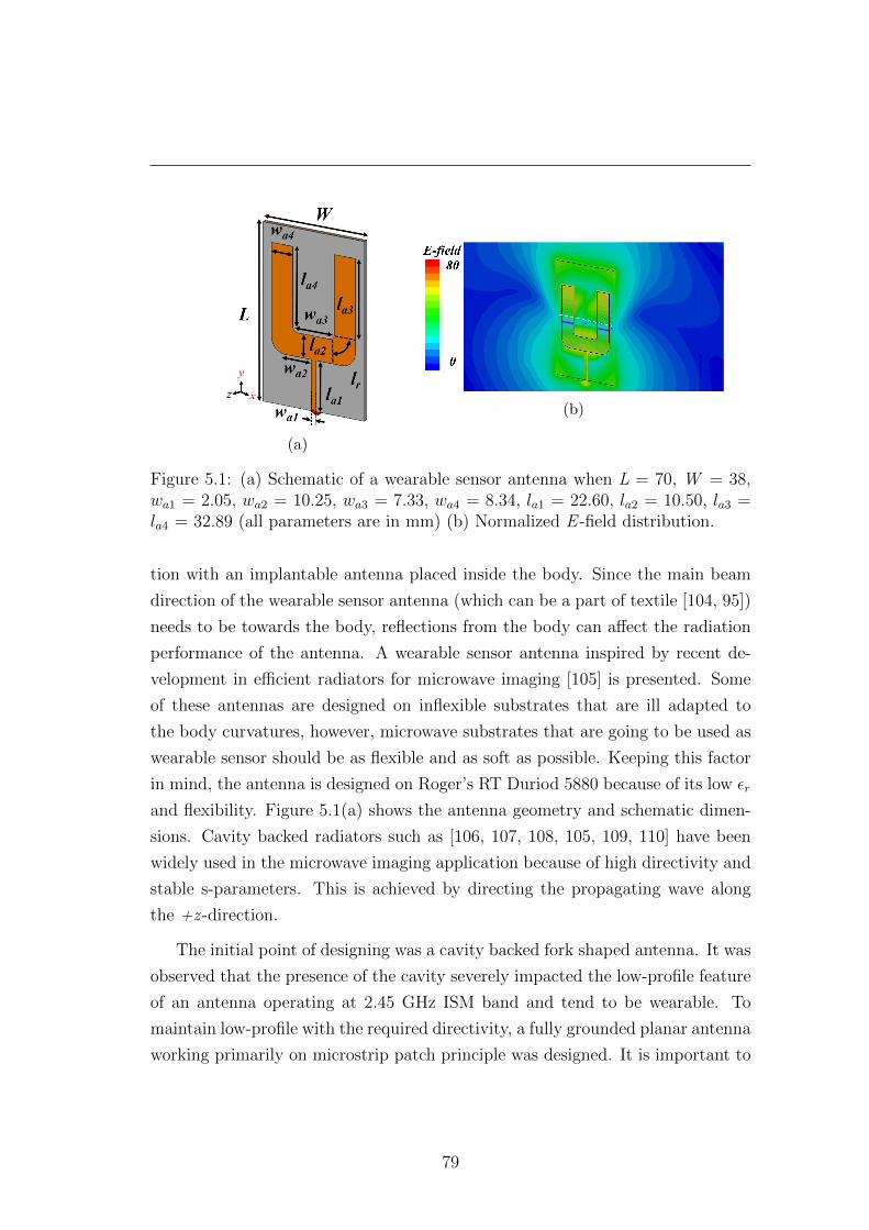
(a)
(b)
Figure 5.1: (a) Schematic of a wearable sensor antenna when L = 70, W = 38,wa1 = 2.05, wa2 = 10.25, wa3 = 7.33, wa4 = 8.34, la1 = 22.60, la2 = 10.50, la3 =la4 = 32.89 (all parameters are in mm) (b) Normalized E -field distribution.
tion with an implantable antenna placed inside the body. Since the main beam
direction of the wearable sensor antenna (which can be a part of textile [104, 95])
needs to be towards the body, reflections from the body can affect the radiation
performance of the antenna. A wearable sensor antenna inspired by recent de-
velopment in efficient radiators for microwave imaging [105] is presented. Some
of these antennas are designed on inflexible substrates that are ill adapted to
the body curvatures, however, microwave substrates that are going to be used as
wearable sensor should be as flexible and as soft as possible. Keeping this factor
in mind, the antenna is designed on Roger’s RT Duriod 5880 because of its low εr
and flexibility. Figure 5.1(a) shows the antenna geometry and schematic dimen-
sions. Cavity backed radiators such as [106, 107, 108, 105, 109, 110] have been
widely used in the microwave imaging application because of high directivity and
stable s-parameters. This is achieved by directing the propagating wave along
the +z -direction.
The initial point of designing was a cavity backed fork shaped antenna. It was
observed that the presence of the cavity severely impacted the low-profile feature
of an antenna operating at 2.45 GHz ISM band and tend to be wearable. To
maintain low-profile with the required directivity, a fully grounded planar antenna
working primarily on microstrip patch principle was designed. It is important to
79
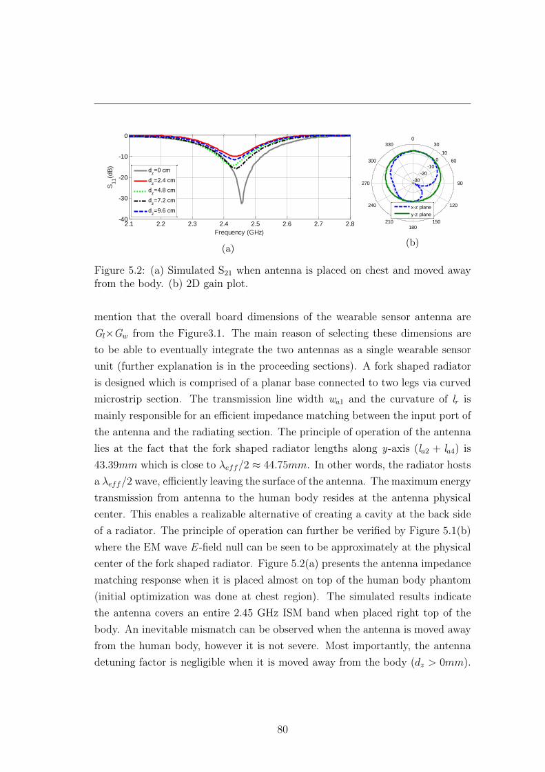
1.5 1.75 2 2.25 2.5 2.75 3-40
-30
-20
-10
0
Frequency(GHz)
S11(d
B)
Meas.
FEM Simu.
FDTD Simu.
1.5 1.75 2 2.25 2.5 2.75 3-80
-60
-40
-20
0
Frequency (GHz)S
-para
mete
r (d
B)
S11
S22
S21
2.1 2.2 2.3 2.4 2.5 2.6 2.7 2.8-40
-30
-20
-10
0
Frequency (GHz)
S1
1(d
B)
dz=0 cm
dz=2.4 cm
dz=4.8 cm
dz=7.2 cm
dz=9.6 cm
1 2 3 4 5 6 7 8 9-80
-70
-60
-50
-40
-30
Positions
S2
1 (
dB
)
Sim.
Analytical
(a)
1.5 1.75 2 2.25 2.5 2.75 3-40
-30
-20
-10
0
Frequency(GHz)
S11(d
B)
Meas.
FEM Simu.
FDTD Simu.
1.5 1.75 2 2.25 2.5 2.75 3-80
-60
-40
-20
0
Frequency (GHz)
S-p
ara
mete
r (d
B)
S11
S22
S21
2.1 2.2 2.3 2.4 2.5 2.6 2.7 2.8-40
-30
-20
-10
0
Frequency (GHz)
S1
1(d
B)
dz=0 cm
dz=2.4 cm
dz=4.8 cm
dz=7.2 cm
dz=9.6 cm
2.1 2.2 2.3 2.4 2.5 2.6 2.7-35
-30
-25
-20
-15
-10
-5
0
Frequency (GHz)
S1
1(d
B)
dz=0 cm
dz=2.4 cm
dz=4.8 cm
dz=7.2 cm
dz=9.6 cm
10
0
-10
-20
-30
030
60
90
120
150180
210
240
270
300
330
x-z plane
y-z plane
(b)
Figure 5.2: (a) Simulated S21 when antenna is placed on chest and moved awayfrom the body. (b) 2D gain plot.
mention that the overall board dimensions of the wearable sensor antenna are
Gl×Gw from the Figure3.1. The main reason of selecting these dimensions are
to be able to eventually integrate the two antennas as a single wearable sensor
unit (further explanation is in the proceeding sections). A fork shaped radiator
is designed which is comprised of a planar base connected to two legs via curved
microstrip section. The transmission line width wa1 and the curvature of lr is
mainly responsible for an efficient impedance matching between the input port of
the antenna and the radiating section. The principle of operation of the antenna
lies at the fact that the fork shaped radiator lengths along y-axis (la2 + la4) is
43.39mm which is close to λeff/2 ≈ 44.75mm. In other words, the radiator hosts
a λeff/2 wave, efficiently leaving the surface of the antenna. The maximum energy
transmission from antenna to the human body resides at the antenna physical
center. This enables a realizable alternative of creating a cavity at the back side
of a radiator. The principle of operation can further be verified by Figure 5.1(b)
where the EM wave E -field null can be seen to be approximately at the physical
center of the fork shaped radiator. Figure 5.2(a) presents the antenna impedance
matching response when it is placed almost on top of the human body phantom
(initial optimization was done at chest region). The simulated results indicate
the antenna covers an entire 2.45 GHz ISM band when placed right top of the
body. An inevitable mismatch can be observed when the antenna is moved away
from the human body, however it is not severe. Most importantly, the antenna
detuning factor is negligible when it is moved away from the body (dz > 0mm).
80
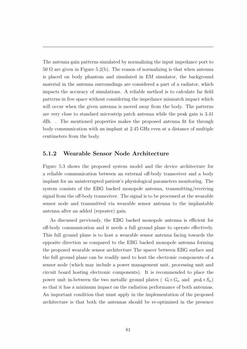
The antenna gain patterns simulated by normalizing the input impedance port to
50 Ω are given in Figure 5.2(b). The reason of normalizing is that when antenna
is placed on body phantom and simulated in EM simulator, the background
material in the antenna surroundings are considered a part of a radiator, which
impacts the accuracy of simulations. A reliable method is to calculate far field
patterns in free space without considering the impedance mismatch impact which
will occur when the given antenna is moved away from the body. The patterns
are very close to standard microstrip patch antenna while the peak gain is 3.41
dBi. . The mentioned properties makes the proposed antenna fit for through
body communication with an implant at 2.45 GHz even at a distance of multiple
centimeters from the body.
5.1.2 Wearable Sensor Node Architecture
Figure 5.3 shows the proposed system model and the device architecture for
a reliable communication between an external off-body transceiver and a body
implant for an uninterrupted patient’s physiological parameters monitoring. The
system consists of the EBG backed monopole antenna, transmitting/receiving
signal from the off-body transceiver. The signal is to be processed at the wearable
sensor node and transmitted via wearable sensor antenna to the implantable
antenna after an added (repeater) gain.
As discussed previously, the EBG backed monopole antenna is efficient for
off-body communication and it needs a full ground plane to operate effectively.
This full ground plane is to host a wearable sensor antenna facing towards the
opposite direction as compared to the EBG backed monopole antenna forming
the proposed wearable sensor architecture The spacer between EBG surface and
the full ground plane can be readily used to host the electronic components of a
sensor node (which may include a power management unit, processing unit and
circuit board hosting electronic components). It is recommended to place the
power unit in-between the two metallic ground plates ( Gl×Gw and gndl×Sw)
so that it has a minimum impact on the radiation performance of both antennas.
An important condition that must apply in the implementation of the proposed
architecture is that both the antennas should be re-optimized in the presence
81
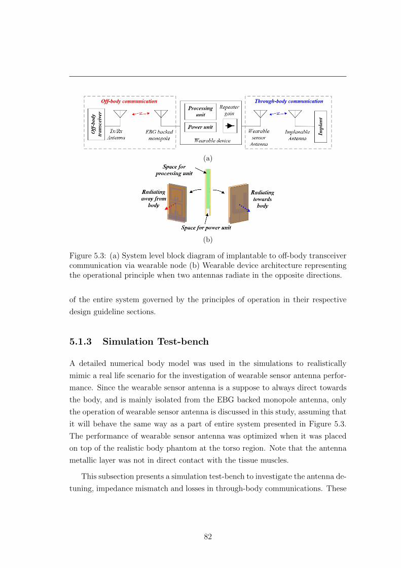
(a)
(b)
Figure 5.3: (a) System level block diagram of implantable to off-body transceivercommunication via wearable node (b) Wearable device architecture representingthe operational principle when two antennas radiate in the opposite directions.
of the entire system governed by the principles of operation in their respective
design guideline sections.
5.1.3 Simulation Test-bench
A detailed numerical body model was used in the simulations to realistically
mimic a real life scenario for the investigation of wearable sensor antenna perfor-
mance. Since the wearable sensor antenna is a suppose to always direct towards
the body, and is mainly isolated from the EBG backed monopole antenna, only
the operation of wearable sensor antenna is discussed in this study, assuming that
it will behave the same way as a part of entire system presented in Figure 5.3.
The performance of wearable sensor antenna was optimized when it was placed
on top of the realistic body phantom at the torso region. Note that the antenna
metallic layer was not in direct contact with the tissue muscles.
This subsection presents a simulation test-bench to investigate the antenna de-
tuning, impedance mismatch and losses in through-body communications. These
82
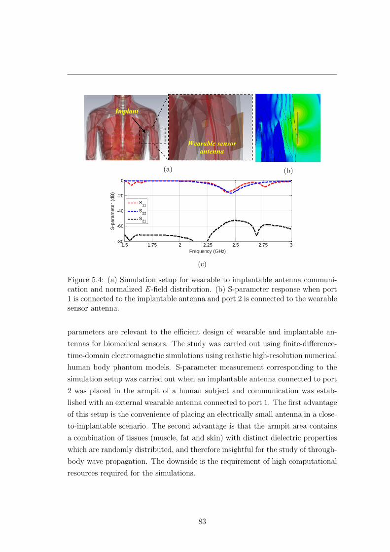
(a) (b)
1.5 1.75 2 2.25 2.5 2.75 3-40
-30
-20
-10
0
Frequency(GHz)
S11(d
B)
Meas.
FEM Simu.
FDTD Simu.
1.5 1.75 2 2.25 2.5 2.75 3-80
-60
-40
-20
0
Frequency (GHz)
S-p
ara
mete
r (d
B)
S11
S22
S21
2.1 2.2 2.3 2.4 2.5 2.6 2.7 2.8-40
-30
-20
-10
0
Frequency (GHz)
S1
1(d
B)
dz=0 cm
dz=2.4 cm
dz=4.8 cm
dz=7.2 cm
dz=9.6 cm
2.1 2.2 2.3 2.4 2.5 2.6 2.7-35
-30
-25
-20
-15
-10
-5
0
Frequency (GHz)
S1
1(d
B)
dz=0 cm
dz=2.4 cm
dz=4.8 cm
dz=7.2 cm
dz=9.6 cm
10
0
-10
-20
-30
030
60
90
120
150180
210
240
270
300
330
x-z plane
y-z plane
(c)
Figure 5.4: (a) Simulation setup for wearable to implantable antenna communi-cation and normalized E -field distribution. (b) S-parameter response when port1 is connected to the implantable antenna and port 2 is connected to the wearablesensor antenna.
parameters are relevant to the efficient design of wearable and implantable an-
tennas for biomedical sensors. The study was carried out using finite-difference-
time-domain electromagnetic simulations using realistic high-resolution numerical
human body phantom models. S-parameter measurement corresponding to the
simulation setup was carried out when an implantable antenna connected to port
2 was placed in the armpit of a human subject and communication was estab-
lished with an external wearable antenna connected to port 1. The first advantage
of this setup is the convenience of placing an electrically small antenna in a close-
to-implantable scenario. The second advantage is that the armpit area contains
a combination of tissues (muscle, fat and skin) with distinct dielectric properties
which are randomly distributed, and therefore insightful for the study of through-
body wave propagation. The downside is the requirement of high computational
resources required for the simulations.
83
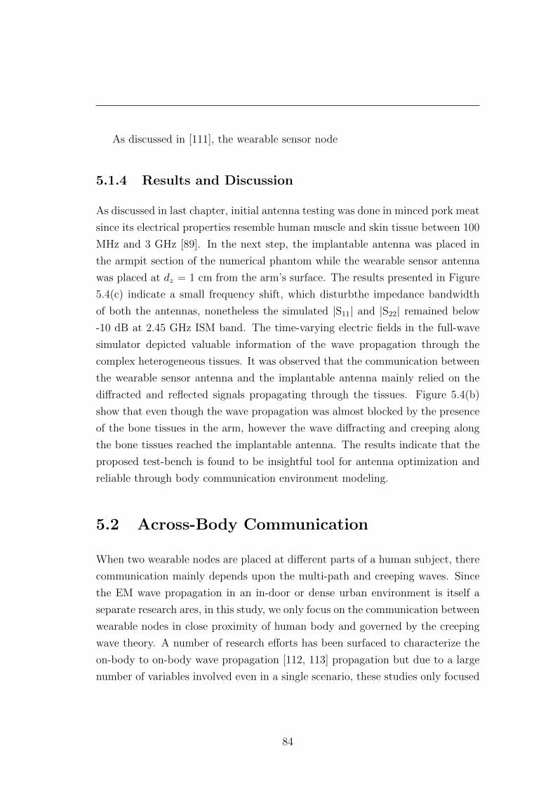
As discussed in [111], the wearable sensor node
5.1.4 Results and Discussion
As discussed in last chapter, initial antenna testing was done in minced pork meat
since its electrical properties resemble human muscle and skin tissue between 100
MHz and 3 GHz [89]. In the next step, the implantable antenna was placed in
the armpit section of the numerical phantom while the wearable sensor antenna
was placed at dz = 1 cm from the arm’s surface. The results presented in Figure
5.4(c) indicate a small frequency shift, which disturbthe impedance bandwidth
of both the antennas, nonetheless the simulated |S11| and |S22| remained below
-10 dB at 2.45 GHz ISM band. The time-varying electric fields in the full-wave
simulator depicted valuable information of the wave propagation through the
complex heterogeneous tissues. It was observed that the communication between
the wearable sensor antenna and the implantable antenna mainly relied on the
diffracted and reflected signals propagating through the tissues. Figure 5.4(b)
show that even though the wave propagation was almost blocked by the presence
of the bone tissues in the arm, however the wave diffracting and creeping along
the bone tissues reached the implantable antenna. The results indicate that the
proposed test-bench is found to be insightful tool for antenna optimization and
reliable through body communication environment modeling.
5.2 Across-Body Communication
When two wearable nodes are placed at different parts of a human subject, there
communication mainly depends upon the multi-path and creeping waves. Since
the EM wave propagation in an in-door or dense urban environment is itself a
separate research ares, in this study, we only focus on the communication between
wearable nodes in close proximity of human body and governed by the creeping
wave theory. A number of research efforts has been surfaced to characterize the
on-body to on-body wave propagation [112, 113] propagation but due to a large
number of variables involved even in a single scenario, these studies only focused
84
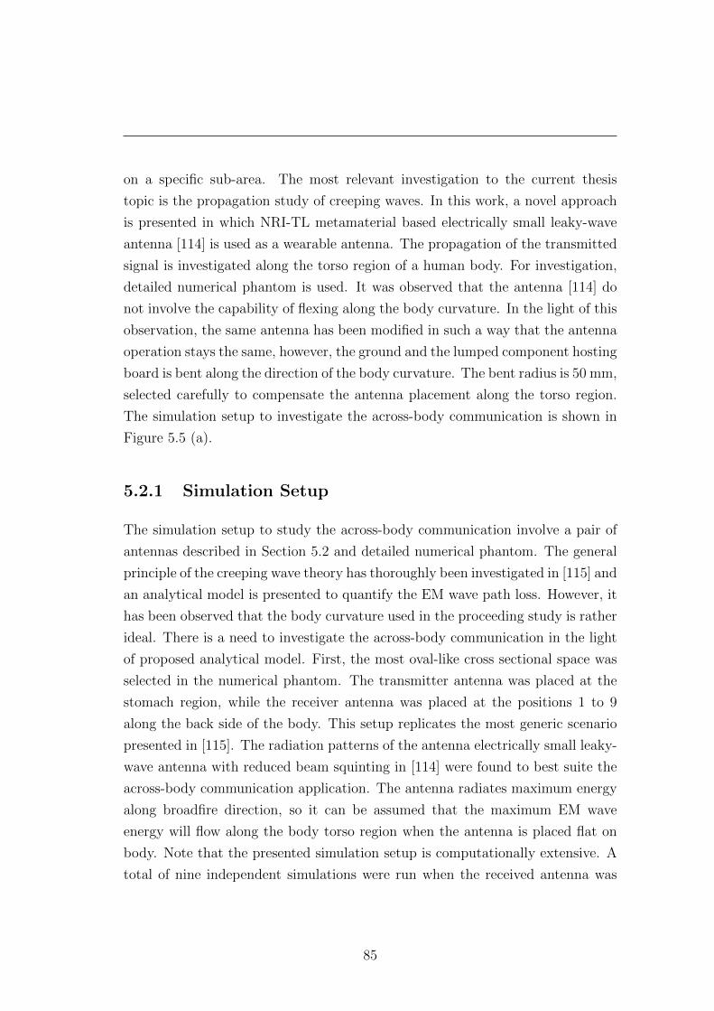
on a specific sub-area. The most relevant investigation to the current thesis
topic is the propagation study of creeping waves. In this work, a novel approach
is presented in which NRI-TL metamaterial based electrically small leaky-wave
antenna [114] is used as a wearable antenna. The propagation of the transmitted
signal is investigated along the torso region of a human body. For investigation,
detailed numerical phantom is used. It was observed that the antenna [114] do
not involve the capability of flexing along the body curvature. In the light of this
observation, the same antenna has been modified in such a way that the antenna
operation stays the same, however, the ground and the lumped component hosting
board is bent along the direction of the body curvature. The bent radius is 50 mm,
selected carefully to compensate the antenna placement along the torso region.
The simulation setup to investigate the across-body communication is shown in
Figure 5.5 (a).
5.2.1 Simulation Setup
The simulation setup to study the across-body communication involve a pair of
antennas described in Section 5.2 and detailed numerical phantom. The general
principle of the creeping wave theory has thoroughly been investigated in [115] and
an analytical model is presented to quantify the EM wave path loss. However, it
has been observed that the body curvature used in the proceeding study is rather
ideal. There is a need to investigate the across-body communication in the light
of proposed analytical model. First, the most oval-like cross sectional space was
selected in the numerical phantom. The transmitter antenna was placed at the
stomach region, while the receiver antenna was placed at the positions 1 to 9
along the back side of the body. This setup replicates the most generic scenario
presented in [115]. The radiation patterns of the antenna electrically small leaky-
wave antenna with reduced beam squinting in [114] were found to best suite the
across-body communication application. The antenna radiates maximum energy
along broadfire direction, so it can be assumed that the maximum EM wave
energy will flow along the body torso region when the antenna is placed flat on
body. Note that the presented simulation setup is computationally extensive. A
total of nine independent simulations were run when the received antenna was
85
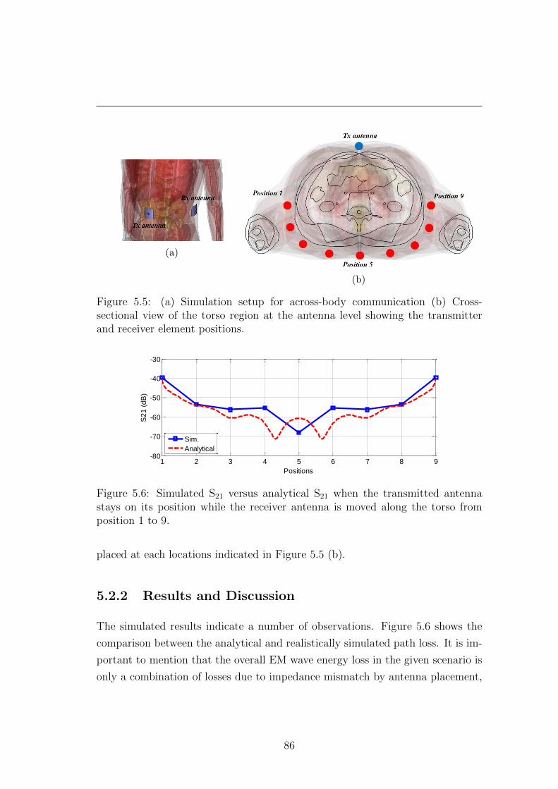
(a)
(b)
Figure 5.5: (a) Simulation setup for across-body communication (b) Cross-sectional view of the torso region at the antenna level showing the transmitterand receiver element positions.
1.5 1.75 2 2.25 2.5 2.75 3-40
-30
-20
-10
0
Frequency(GHz)
S11(d
B)
Meas.
FEM Simu.
FDTD Simu.
1.5 1.75 2 2.25 2.5 2.75 3-80
-60
-40
-20
0
Frequency (GHz)
S-p
ara
mete
r (d
B)
S11
S22
S21
1 2 3 4 5 6 7 8 9-80
-70
-60
-50
-40
-30
Positions
S2
1 (
dB
)
Sim.
Analytical
Figure 5.6: Simulated S21 versus analytical S21 when the transmitted antennastays on its position while the receiver antenna is moved along the torso fromposition 1 to 9.
placed at each locations indicated in Figure 5.5 (b).
5.2.2 Results and Discussion
The simulated results indicate a number of observations. Figure 5.6 shows the
comparison between the analytical and realistically simulated path loss. It is im-
portant to mention that the overall EM wave energy loss in the given scenario is
only a combination of losses due to impedance mismatch by antenna placement,
86
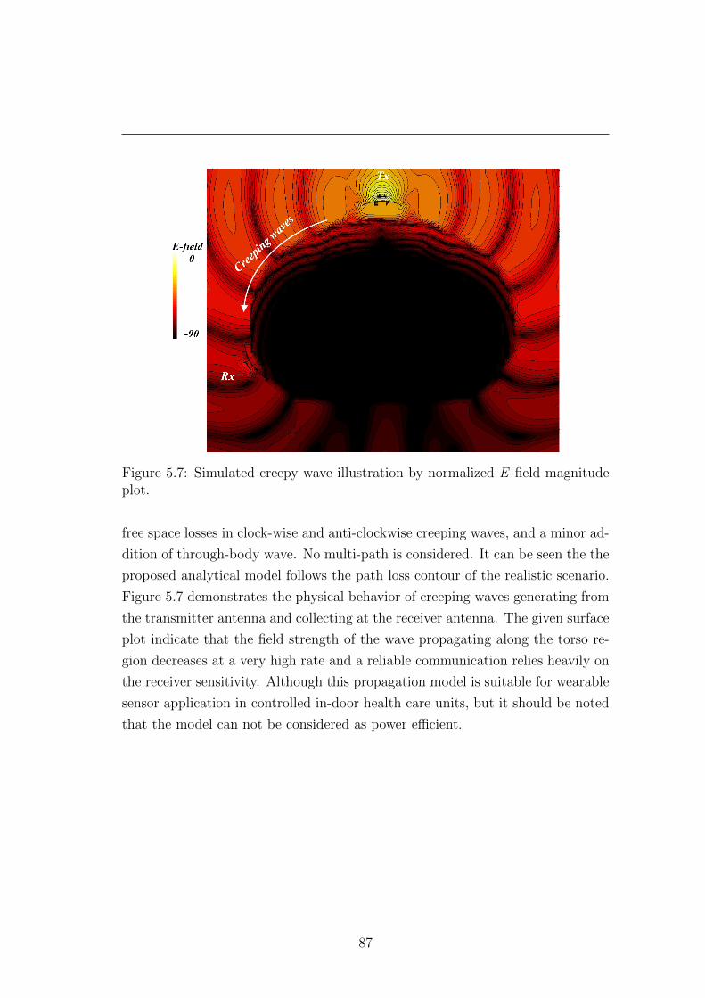
Figure 5.7: Simulated creepy wave illustration by normalized E -field magnitudeplot.
free space losses in clock-wise and anti-clockwise creeping waves, and a minor ad-
dition of through-body wave. No multi-path is considered. It can be seen the the
proposed analytical model follows the path loss contour of the realistic scenario.
Figure 5.7 demonstrates the physical behavior of creeping waves generating from
the transmitter antenna and collecting at the receiver antenna. The given surface
plot indicate that the field strength of the wave propagating along the torso re-
gion decreases at a very high rate and a reliable communication relies heavily on
the receiver sensitivity. Although this propagation model is suitable for wearable
sensor application in controlled in-door health care units, but it should be noted
that the model can not be considered as power efficient.
87
Chapter 6
Miniaturized Ultra Wideband
Antenna
Three planar, CPW-fed, Ultra Wideband (UWB) antennas with increasingly re-
duced size are presented and the miniaturization method is discussed. The first
antenna is a CPW-fed elliptical slot with an uneven U-shaped tuning stub, the
second antenna is a cactus shaped monopole and the third one is a miniaturized
version of the cactus shaped monopole antenna. All presented antennas have a
simulated and measured return loss below -10 dB over the 3.1 to 10.6 GHz UWB
frequency range and mostly omni-directional radiation patterns. The proposed
antennas are fabricated on liquid crystal polymer (LCP). The CPW-fed slot an-
tenna requires an overall board dimension of 38 mm × 40 mm, the evolved cactus
monopole is confined in a 28 mm × 32 mm board, while the final miniaturized
cactus monopole is printed on 28 mm× 20 mm board, resulting in a 41 % and 63%
size reduction respectively. Using both simulations and measurements the paper
analyzes the response of all three antennas, and discusses, and demonstrates the
effectiveness of the implemented miniaturization method.
88
6.1 Introduction on UWB Antennass
The Ultra Wide Band protocol that covers the frequency range from 3.1-10.6
GHz was released from the FCC in 2002 [116], partly as an attempt to meet the
demand for high data rate communications in short distances for mobile and per-
sonal applications. Consequently, there is an increasing need for compact sized,
low cost and high efficiency antennas with omni-directional radiation patterns.
The combination of these characteristics in a wide frequency range such as the
UWB band is a challenging problem and several design concepts and different
materials have been used in an attempt to provide a satisfactory solution. The
challenge associated with the miniaturization of antennas has been the tradeoff
between the reduction of the physical size of the antenna and its operational
bandwidth [117] and radiation efficiency. Some researchers have adopted the use
of substrates with relatively high dielectric constant to reduce the antenna’s reso-
nant frequency because permittivity is inversely related to the resonant frequency
[118]. However, bandwidth reduction is inevitable in this approach because band-
width is also inversely proportional to the permittivity. In an attempt to increase
the bandwidth of an antenna and cover the whole UWB frequency range, configu-
rations like planar monopoles [119, 120, 121], slot fed IF (inverted F) [122], CPW
fed monopole[120, 49, 123, 124, 125], U-shaped elliptical slot [126], patch array
with energy band gap (EBG) structures [118] and CPW fed fractal antenna [127]
have been proposed. Also the effects of printed UWB antenna miniaturization on
transmitted time domain pulse fidelity and pattern stability have been recently
discussed in [128]. In several papers [117, 119, 129, 130] it has been demonstrated
that by following certain miniaturization guidelines, compact planar UWB anten-
nas can be made. Numerous planner UWB antennas and band-notch UWB quasi-
monopole antennas have illustrated symmetrical shapes[125, 128, 131]. In these
structures, two symmetrical halves exhibits two identical strong current paths. It
has been noted that the current distribution patterns in these structures replicate
the conditions of magnetic mirror symmetry. Chopping off half of the symmetrical
monopole antenna provides a straight forward miniaturization. It has also been
explored that by having one strong current path, antenna exhibits an even wider
bandwidth[128, 131, 132], however, not all half cut UWB structures can achieve
89
a suitable impedance matching over a wide bandwidth. A further modification to
the feeding structure is required for a better impedance matching [132]. Increaser
in cross-polarization level is reported to be a major limitation in this miniatur-
ization technique [131]. Another configuration of self-complementary antenna
(SCA) has stimulated a considerable attention for low profile UWB applications.
Theoretically, a wideband operation is obtained when an antenna and its com-
plement are identical, providing a constant input impedance independent of the
antenna geometry and frequency. Some recent efforts have been devoted to use
SCA antenna for UWB application. Antennas formed by a self-complementing
semi-circular monopole [133, 134, 135], quarter-circular monopole[136, 137], ob-
tuse pie-shaped monopole [138], compact bow-tie [139] and Γ-shaped radiator
[140] has been proposed and studied. In addition to the impressive theoretical
prospective of SCAs, it has to be reported that a matching network is always
required to match the antenna to a 50 ohm feed line. This has limited the use of
SCAs for miniaturized UWB antennas since the matching network is indispens-
able. In this paper, a simple procedure in aggregation with previously proposed
guidelines is used to miniaturize an elliptical slot UWB planner antenna. The
initial design is similar to the one proposed in [126] whereas the final novel design
is a CPW-fed cactus shaped UWB antenna having dimensions 20 mm × 28 mm.
It is worth mentioning that the final miniaturized UWB cactus antenna is rather
compact in size and exhibits wider bandwidth as compared to similar structures
presented in [141, 142, 143, 144] while fabricated on lower εr material (LCP).
6.1.1 Electrically Small UWB Antenna Designs
The UWB antennas are presented in Figure 6.1. They are fabricated on low loss
(tanδ=0.002), low dielectric constant (εr=3), LCP with a copper layer that is 18
µm thick. The CPW-fed slot antenna is fabricated on a 350 µm thick substrate
while for the cactus antenna and the miniaturized cactus antenna a thinner 225
µm thick substrate was used. At the early stages of the design procedure, it
was observed that the 350 µm thick paper substrate exhibit rigidness. To make
the cactus antenna conformal as well as miniaturized, substrate thickness was re-
duced. By specifying the angle and rate of LCP extrusion while manufacturing,
90
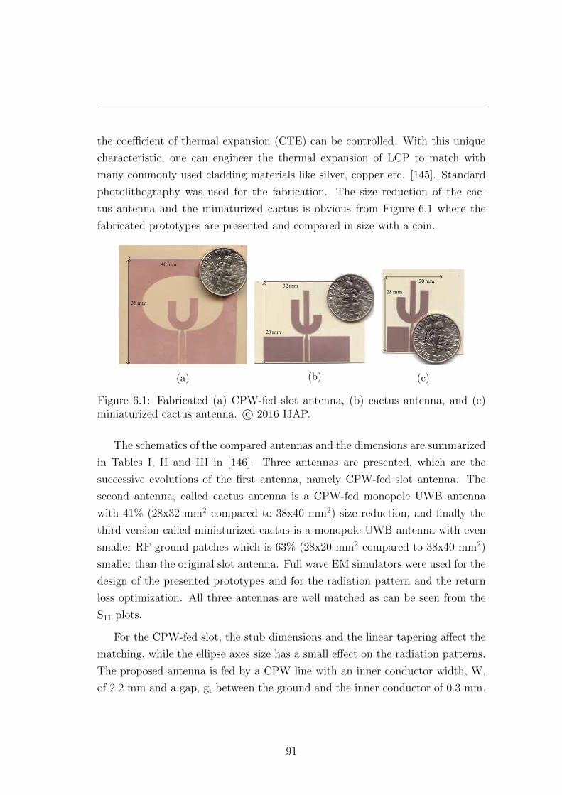
the coefficient of thermal expansion (CTE) can be controlled. With this unique
characteristic, one can engineer the thermal expansion of LCP to match with
many commonly used cladding materials like silver, copper etc. [145]. Standard
photolithography was used for the fabrication. The size reduction of the cac-
tus antenna and the miniaturized cactus is obvious from Figure 6.1 where the
fabricated prototypes are presented and compared in size with a coin.
40mm
38mm
(a)
28mm
32mm
(b)
20mm
28mm
(c)
Figure 6.1: Fabricated (a) CPW-fed slot antenna, (b) cactus antenna, and (c)miniaturized cactus antenna. c© 2016 IJAP.
The schematics of the compared antennas and the dimensions are summarized
in Tables I, II and III in [146]. Three antennas are presented, which are the
successive evolutions of the first antenna, namely CPW-fed slot antenna. The
second antenna, called cactus antenna is a CPW-fed monopole UWB antenna
with 41% (28x32 mm2 compared to 38x40 mm2) size reduction, and finally the
third version called miniaturized cactus is a monopole UWB antenna with even
smaller RF ground patches which is 63% (28x20 mm2 compared to 38x40 mm2)
smaller than the original slot antenna. Full wave EM simulators were used for the
design of the presented prototypes and for the radiation pattern and the return
loss optimization. All three antennas are well matched as can be seen from the
S11 plots.
For the CPW-fed slot, the stub dimensions and the linear tapering affect the
matching, while the ellipse axes size has a small effect on the radiation patterns.
The proposed antenna is fed by a CPW line with an inner conductor width, W,
of 2.2 mm and a gap, g, between the ground and the inner conductor of 0.3 mm.
91
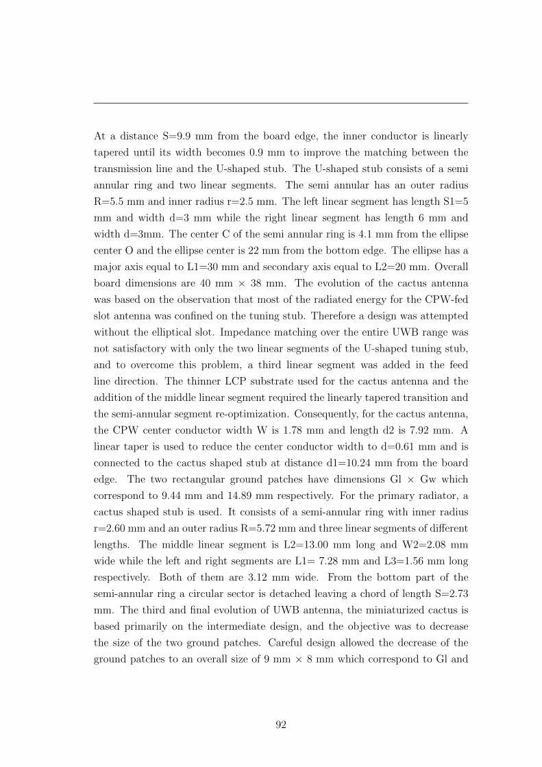
At a distance S=9.9 mm from the board edge, the inner conductor is linearly
tapered until its width becomes 0.9 mm to improve the matching between the
transmission line and the U-shaped stub. The U-shaped stub consists of a semi
annular ring and two linear segments. The semi annular has an outer radius
R=5.5 mm and inner radius r=2.5 mm. The left linear segment has length S1=5
mm and width d=3 mm while the right linear segment has length 6 mm and
width d=3mm. The center C of the semi annular ring is 4.1 mm from the ellipse
center O and the ellipse center is 22 mm from the bottom edge. The ellipse has a
major axis equal to L1=30 mm and secondary axis equal to L2=20 mm. Overall
board dimensions are 40 mm × 38 mm. The evolution of the cactus antenna
was based on the observation that most of the radiated energy for the CPW-fed
slot antenna was confined on the tuning stub. Therefore a design was attempted
without the elliptical slot. Impedance matching over the entire UWB range was
not satisfactory with only the two linear segments of the U-shaped tuning stub,
and to overcome this problem, a third linear segment was added in the feed
line direction. The thinner LCP substrate used for the cactus antenna and the
addition of the middle linear segment required the linearly tapered transition and
the semi-annular segment re-optimization. Consequently, for the cactus antenna,
the CPW center conductor width W is 1.78 mm and length d2 is 7.92 mm. A
linear taper is used to reduce the center conductor width to d=0.61 mm and is
connected to the cactus shaped stub at distance d1=10.24 mm from the board
edge. The two rectangular ground patches have dimensions Gl × Gw which
correspond to 9.44 mm and 14.89 mm respectively. For the primary radiator, a
cactus shaped stub is used. It consists of a semi-annular ring with inner radius
r=2.60 mm and an outer radius R=5.72 mm and three linear segments of different
lengths. The middle linear segment is L2=13.00 mm long and W2=2.08 mm
wide while the left and right segments are L1= 7.28 mm and L3=1.56 mm long
respectively. Both of them are 3.12 mm wide. From the bottom part of the
semi-annular ring a circular sector is detached leaving a chord of length S=2.73
mm. The third and final evolution of UWB antenna, the miniaturized cactus is
based primarily on the intermediate design, and the objective was to decrease
the size of the two ground patches. Careful design allowed the decrease of the
ground patches to an overall size of 9 mm × 8 mm which correspond to Gl and
92
Gw respectively. The description of the miniaturized cactus design is similar to
the presented description for the cactus antenna. As a result of the ground size
reduction, further tuning was needed for the three stubs that consist the cactus
shaped radiating element.
The overall board dimensions for the cactus antenna is 32 mm × 28 mm,
resulting in a 41% reduction in area compared to the CPW-fed slot while the
miniaturized cactus has overall board dimensions 28 mm × 20 mm resulting in
63% size reduction compared to the slot antenna. For the antenna dimensions,
the common variables’ names are set independently for each antenna schematic
and must not be related.
6.1.2 Miniaturization Procedure
The size reduction was envisioned by the investigation of the surface current dis-
tribution on the slot antenna. It was observed that the radiation was primarily
caused by the current distribution on the U-shaped stub (Figures 4a, 4b), al-
though the elliptical slot also contributes, to a lesser extent. The surface current
distributions on the two cactus antennas (Figures 4c-4f) have a similar form with
the one on the U-shaped stub, something that explains the similarity in the re-
sulted radiation patterns. Based on the surface current distribution observations,
and trying to improve the matching the even U-shaped stub (Ant1 from Figure
6.3) was replaced with an uneven U-shaped stub. The added perturbation on
the tuning stub added one design degree of freedom that allowed the improve-
ment of the matching as can be seen in Figure 6.4. The uneven U-shaped slot,
which is presented in Figure 6.3 under the name Ant2 had improved matching
as can be seen in the S11 plots of Figure 6.3. In the next iteration (Ant3) the
slot was removed, and in order to further improve the matching for the remained
U-shaped stub, a third tuning stub was added, along the direction of the feed line,
resulting in the cactus shaped radiator (Ant4) that evolved eventually, after some
additional tuning, to the miniaturized cactus antenna. This third middle stub
allowed for an additional design parameter and as a result of its bigger length the
matching in the lower end of the UWB range, in the area around 3.1 GHz could
be improved. The matching improvement in the lower frequency end, is evident
93
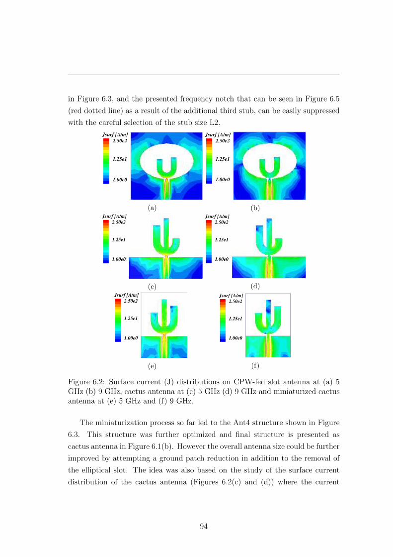
in Figure 6.3, and the presented frequency notch that can be seen in Figure 6.5
(red dotted line) as a result of the additional third stub, can be easily suppressed
with the careful selection of the stub size L2.
Jsurf [A/m]
2.50e2
1.25e1
1.00e0
(a)
Jsurf [A/m]
2.50e2
1.25e1
1.00e0
(b)Jsurf [A/m]
2.50e2
1.25e1
1.00e0
(c)
Jsurf [A/m]
2.50e2
1.25e1
1.00e0
(d)Jsurf [A/m]
2.50e2
1.25e1
1.00e0
(e)
Jsurf [A/m]
2.50e2
1.25e1
1.00e0
(f)
Figure 6.2: Surface current (J) distributions on CPW-fed slot antenna at (a) 5GHz (b) 9 GHz, cactus antenna at (c) 5 GHz (d) 9 GHz and miniaturized cactusantenna at (e) 5 GHz and (f) 9 GHz.
The miniaturization process so far led to the Ant4 structure shown in Figure
6.3. This structure was further optimized and final structure is presented as
cactus antenna in Figure 6.1(b). However the overall antenna size could be further
improved by attempting a ground patch reduction in addition to the removal of
the elliptical slot. The idea was also based on the study of the surface current
distribution of the cactus antenna (Figures 6.2(c) and (d)) where the current
94
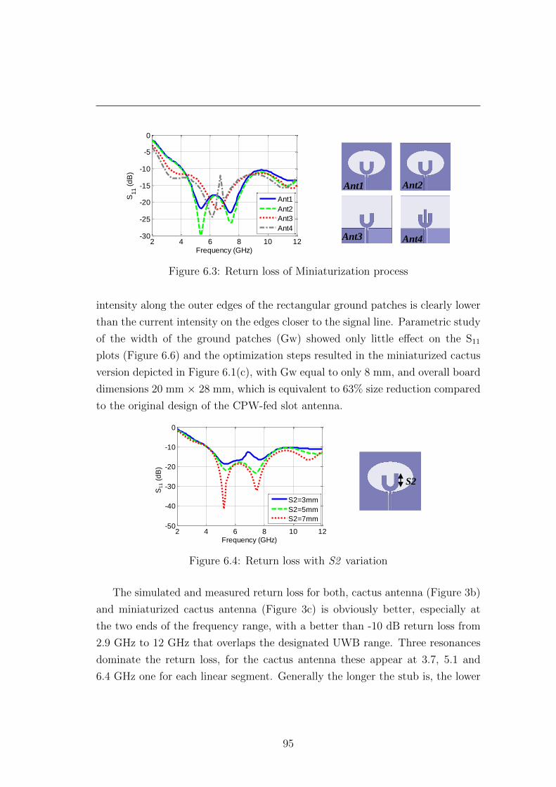
Figure 5. S11 of Miniaturization process
2 4 6 8 10 12-30
-25
-20
-15
-10
-5
0
Frequency (GHz)
S11 (
dB
)
Ant1
Ant2
Ant3
Ant4
Ant1 Ant2
Ant4 Ant3
Figure 6.3: Return loss of Miniaturization process
intensity along the outer edges of the rectangular ground patches is clearly lower
than the current intensity on the edges closer to the signal line. Parametric study
of the width of the ground patches (Gw) showed only little effect on the S11
plots (Figure 6.6) and the optimization steps resulted in the miniaturized cactus
version depicted in Figure 6.1(c), with Gw equal to only 8 mm, and overall board
dimensions 20 mm × 28 mm, which is equivalent to 63% size reduction compared
to the original design of the CPW-fed slot antenna.
Figure 6. S11 with S2 variation
-502 4 6 8 10 12
-40
-30
-20
-10
0
Frequency (GHz)
S1
1 (
dB
)
S2=3mm
S2=5mm
S2=7mm
S2
Figure 6.4: Return loss with S2 variation
The simulated and measured return loss for both, cactus antenna (Figure 3b)
and miniaturized cactus antenna (Figure 3c) is obviously better, especially at
the two ends of the frequency range, with a better than -10 dB return loss from
2.9 GHz to 12 GHz that overlaps the designated UWB range. Three resonances
dominate the return loss, for the cactus antenna these appear at 3.7, 5.1 and
6.4 GHz one for each linear segment. Generally the longer the stub is, the lower
95
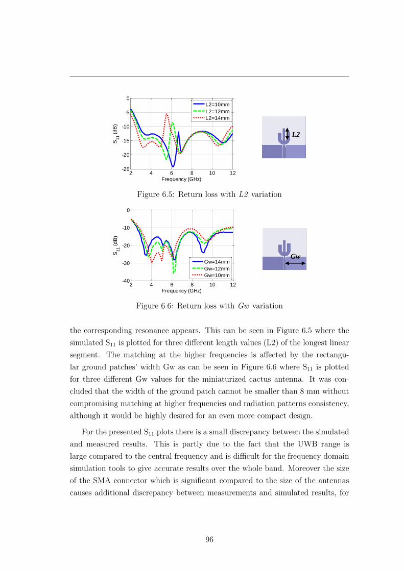
Figure 7. S11 with L2 variation
2 4 6 8 10 12-25
-20
-15
-10
-5
0
Frequency (GHz)
S11 (
dB
)
L2=10mm
L2=12mm
L2=14mm
L2
Figure 6.5: Return loss with L2 variation
Figure 8. S11 with ground width (Gw) variation
2 4 6 8 10 12-40
-30
-20
-10
0
Frequency (GHz)
S11 (
dB
)
Gw=14mm
Gw=12mm
Gw=10mm
Gw
Figure 6.6: Return loss with Gw variation
the corresponding resonance appears. This can be seen in Figure 6.5 where the
simulated S11 is plotted for three different length values (L2) of the longest linear
segment. The matching at the higher frequencies is affected by the rectangu-
lar ground patches’ width Gw as can be seen in Figure 6.6 where S11 is plotted
for three different Gw values for the miniaturized cactus antenna. It was con-
cluded that the width of the ground patch cannot be smaller than 8 mm without
compromising matching at higher frequencies and radiation patterns consistency,
although it would be highly desired for an even more compact design.
For the presented S11 plots there is a small discrepancy between the simulated
and measured results. This is partly due to the fact that the UWB range is
large compared to the central frequency and is difficult for the frequency domain
simulation tools to give accurate results over the whole band. Moreover the size
of the SMA connector which is significant compared to the size of the antennas
causes additional discrepancy between measurements and simulated results, for
96
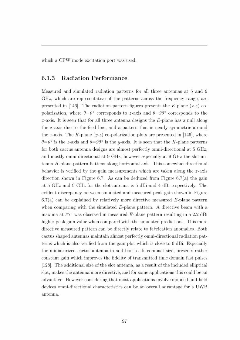
which a CPW mode excitation port was used.
6.1.3 Radiation Performance
Measured and simulated radiation patterns for all three antennas at 5 and 9
GHz, which are representative of the patterns across the frequency range, are
presented in [146]. The radiation pattern figures presents the E -plane (x-z ) co-
polarization, where θ=0 corresponds to z -axis and θ=90 corresponds to the
x -axis. It is seen that for all three antenna designs the E -plane has a null along
the x -axis due to the feed line, and a pattern that is nearly symmetric around
the x -axis. The H -plane (y-z ) co-polarization plots are presented in [146], where
θ=0 is the z -axis and θ=90 is the y-axis. It is seen that the H -plane patterns
for both cactus antenna designs are almost perfectly omni-directional at 5 GHz,
and mostly omni-directional at 9 GHz, however especially at 9 GHz the slot an-
tenna H -plane pattern flattens along horizontal axis. This somewhat directional
behavior is verified by the gain measurements which are taken along the z -axis
direction shown in Figure 6.7. As can be deduced from Figure 6.7(a) the gain
at 5 GHz and 9 GHz for the slot antenna is 5 dBi and 4 dBi respectively. The
evident discrepancy between simulated and measured peak gain shown in Figure
6.7(a) can be explained by relatively more directive measured E -plane pattern
when comparing with the simulated E -plane pattern. A directive beam with a
maxima at 37 was observed in measured E -plane pattern resulting in a 2.2 dBi
higher peak gain value when compared with the simulated predictions. This more
directive measured pattern can be directly relate to fabrication anomalies. Both
cactus shaped antennas maintain almost perfectly omni-directional radiation pat-
terns which is also verified from the gain plot which is close to 0 dBi. Especially
the miniaturized cactus antenna in addition to its compact size, presents rather
constant gain which improves the fidelity of transmitted time domain fast pulses
[128]. The additional size of the slot antenna, as a result of the included elliptical
slot, makes the antenna more directive, and for some applications this could be an
advantage. However considering that most applications involve mobile hand-held
devices omni-directional characteristics can be an overall advantage for a UWB
antenna.
97
(a) (b)
(c) (d)
Figure 11: Simulated and measured gain comparison for (a) CPW-fed slot antenna (b) Cactus antenna
(c) Miniaturization cactus antenna and (d) Comparison of measured gain for all three antennas
4 6 8 10-2
0
2
4
6
Frequency (GHz)
Ga
in (
dB
i)
Measurement
Simulation
4 6 8 10-4
-2
0
2
4
Frequency (GHz)
Ga
in (
dB
i)
Measurement
Simulation
4 6 8 10-2
-1
0
1
2
3
4
Frequency (GHz)
Ga
in (
dB
i)
Measured
Simulated
4 6 8 10-8
-6
-4
-2
0
2
4
6
Frequency (GHz)
Ga
in (
dB
i)
CPW-fed slot antenna
Cactus antenna
Miniaturized cactus antenna
(a)
(a) (b)
(c) (d)
Figure 11: Simulated and measured gain comparison for (a) CPW-fed slot antenna (b) Cactus antenna
(c) Miniaturization cactus antenna and (d) Comparison of measured gain for all three antennas
4 6 8 10-4
-2
0
2
4
Frequency (GHz)
Ga
in (
dB
i)
Measurement
Simulation
4 6 8 10-4
-2
0
2
4
Frequency (GHz)
Ga
in (
dB
i)
Measurement
Simulation
4 6 8 10-2
-1
0
1
2
3
4
Frequency (GHz)
Ga
in (
dB
i)
Measured
Simulated
4 6 8 10-8
-6
-4
-2
0
2
4
6
Frequency (GHz)
Ga
in (
dB
i)
CPW-fed slot antenna
Cactus antenna
Miniaturized cactus antenna
(b)
(a) (b)
(c) (d)
Figure 11: Simulated and measured gain comparison for (a) CPW-fed slot antenna (b) Cactus antenna
(c) Miniaturization cactus antenna and (d) Comparison of measured gain for all three antennas
4 6 8 10-4
-2
0
2
4
Frequency (GHz)
Ga
in (
dB
i)
Measurement
Simulation
4 6 8 10-4
-2
0
2
4
Frequency (GHz)
Ga
in (
dB
i)
Measurement
Simulation
4 6 8 10-2
-1
0
1
2
3
4
Frequency (GHz)
Ga
in (
dB
i)
Measured
Simulated
4 6 8 10-8
-6
-4
-2
0
2
4
6
Frequency (GHz)
Ga
in (
dB
i)
CPW-fed slot antenna
Cactus antenna
Miniaturized cactus antenna
(c)
(a) (b)
(c) (d)
Figure 11: Simulated and measured gain comparison for (a) CPW-fed slot antenna (b) Cactus antenna
(c) Miniaturization cactus antenna and (d) Comparison of measured gain for all three antennas
4 6 8 10-4
-2
0
2
4
Frequency (GHz)
Ga
in (
dB
i)
Measurement
Simulation
4 6 8 10-4
-2
0
2
4
Frequency (GHz)
Ga
in (
dB
i)
Measurement
Simulation
4 6 8 10-2
-1
0
1
2
3
4
Frequency (GHz)
Ga
in (
dB
i)
Measured
Simulated
4 6 8 10-8
-6
-4
-2
0
2
4
6
Frequency (GHz)
Ga
in (
dB
i)
CPW-fed slot antenna
Cactus antenna
Miniaturized cactus antenna
(d)
Figure 6.7: Simulated and measured gain comparison for (a) CPW -fed slot an-tenna (b) Cactus antenna (c) Miniaturization cactus antenna and (d) Comparisonof measured gain for all three antennas
6.2 Miniaturized Cactus-shaped Antenna
This section presents an in depth study on novel cactus-shaped Ultra Wideband
(UWB) monopole antenna fabricated on Liquid Crystal Polymer (Figure 6.1(c))
(LCP) as a next step to the miniaturization of large size UWB antenna. The
proposed antenna is a very compact design since it can be fabricated on a board
with dimensions only 20×28 mm2, while the three linear segments that comprise
the cactus-shaped monopole provide a direct control on antenna matching. The
proposed antenna is operating from 2.85 GHz to 11.85 GHz and it presents very
consistent omni-directional patterns throughout the UWB frequency range. Re-
turn loss and pattern measurements are presented and the operation principles
are discussed in detail. The simplicity of this topology, with the easily control-
lable return loss, allows for its easy implementation for various UWB sub-band
98
designs, just by building suitable monopole versions, for which the only difference
is the length of the three linear segments.
Since the FCC [116] regulated the 3.1–10.6 GHz band for UWB applications,
a significant amount of research activity has been recorded in the area of the
design and implementation of UWB antennas. Depending on the application,
the requirements for antenna designing may vary significantly, however, for wire-
less applications, especially for mobile handheld devices, the small size and the
omni-directional pattern are highly demanded. For the omni-directional pattern
requirements the solution of the printed monopole has been proven very pop-
ular and adequately efficient. A circular disk monopole proposed in [147, 148]
provides consistent omni-directional pattern, however it does not provide any
control on the return loss that would potentially allow the operation of the an-
tenna in desired UWB sub-bands (lower and higher). A direct control on the
return loss and therefore on the radiated frequencies is achieved by the CPW-
fed hexagonal antenna presented in [149] and the composite right/left-handed
(DCRLH) transmission line loaded antenna [150], which are used for multi-band
applications. CPW-fed monopole and electromagnetic band-gap (EBG) combi-
nation antenna that features multi-band and wideband behavior is introduced
in [151, 152], while CPW-fed monopole with parasitic circular-hat patch is used
for the broadband operation in [153] and the L-shaped monopole antenna with
hexagonal slot is demonstrated in [154]. However, none of the aforementioned
antennas covers the whole UWB range. Microstrip line fed Fork-shaped [142],
U-shaped [155], pentagon-shaped [156] and CPW-fed bowled-shaped [120] pla-
nar monopole antennas that cover the whole UWB range have been presented in
recent years, however all of these antennas are almost two times the size of the
proposed cactus-shaped monopole.
In next sections, a compact cactus-shaped monopole UWB antenna is pro-
posed. The presented prototype has board dimensions, 20×28 mm2, is fabricated
on low εr flexible organic dielectric material (LCP with εr=3),presents consistent
omni-directional patterns in H -plane, and allows direct control on the return
loss. The radiation mechanism and the wide band operation are explained in
detail, while return loss, pattern and gain measurements are presented to verify
99
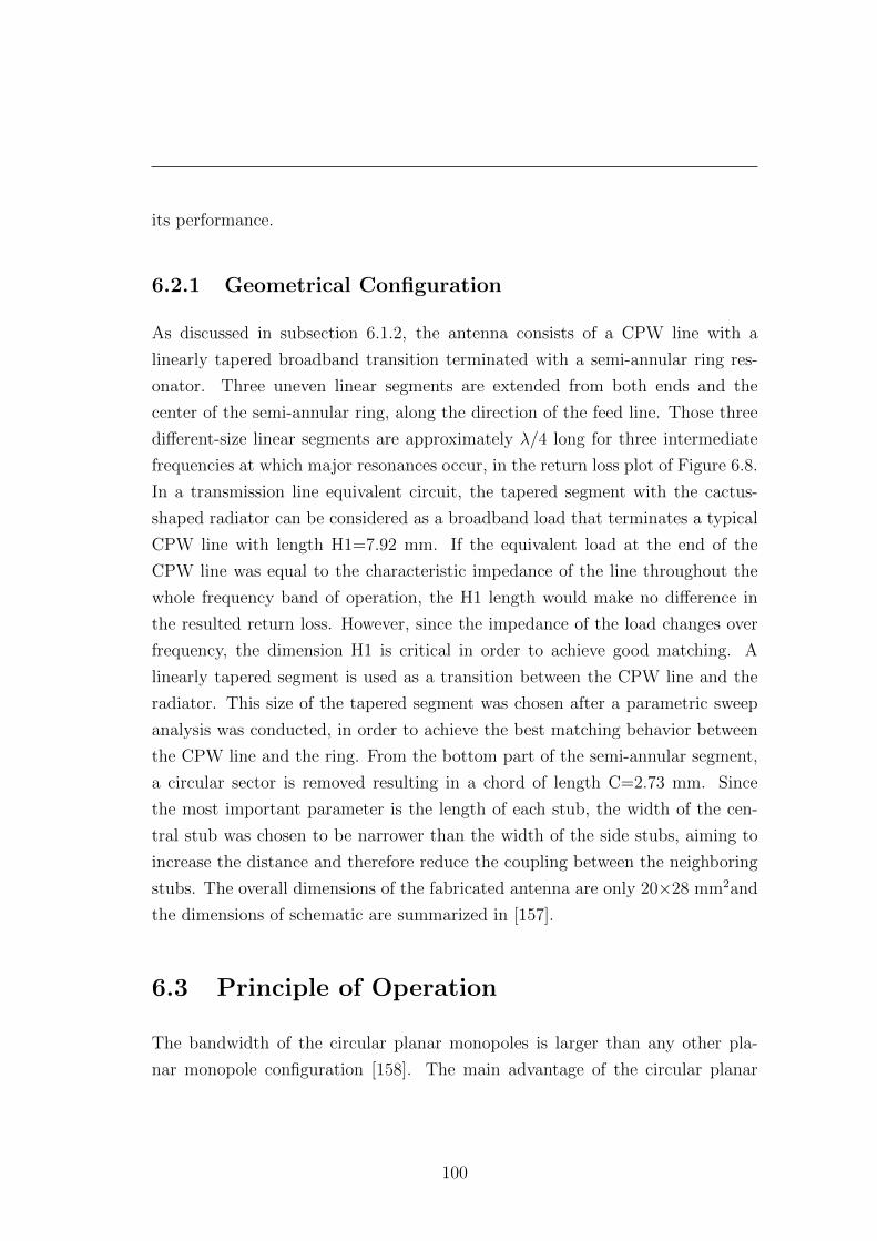
its performance.
6.2.1 Geometrical Configuration
As discussed in subsection 6.1.2, the antenna consists of a CPW line with a
linearly tapered broadband transition terminated with a semi-annular ring res-
onator. Three uneven linear segments are extended from both ends and the
center of the semi-annular ring, along the direction of the feed line. Those three
different-size linear segments are approximately λ/4 long for three intermediate
frequencies at which major resonances occur, in the return loss plot of Figure 6.8.
In a transmission line equivalent circuit, the tapered segment with the cactus-
shaped radiator can be considered as a broadband load that terminates a typical
CPW line with length H1=7.92 mm. If the equivalent load at the end of the
CPW line was equal to the characteristic impedance of the line throughout the
whole frequency band of operation, the H1 length would make no difference in
the resulted return loss. However, since the impedance of the load changes over
frequency, the dimension H1 is critical in order to achieve good matching. A
linearly tapered segment is used as a transition between the CPW line and the
radiator. This size of the tapered segment was chosen after a parametric sweep
analysis was conducted, in order to achieve the best matching behavior between
the CPW line and the ring. From the bottom part of the semi-annular segment,
a circular sector is removed resulting in a chord of length C=2.73 mm. Since
the most important parameter is the length of each stub, the width of the cen-
tral stub was chosen to be narrower than the width of the side stubs, aiming to
increase the distance and therefore reduce the coupling between the neighboring
stubs. The overall dimensions of the fabricated antenna are only 20×28 mm2and
the dimensions of schematic are summarized in [157].
6.3 Principle of Operation
The bandwidth of the circular planar monopoles is larger than any other pla-
nar monopole configuration [158]. The main advantage of the circular planar
100
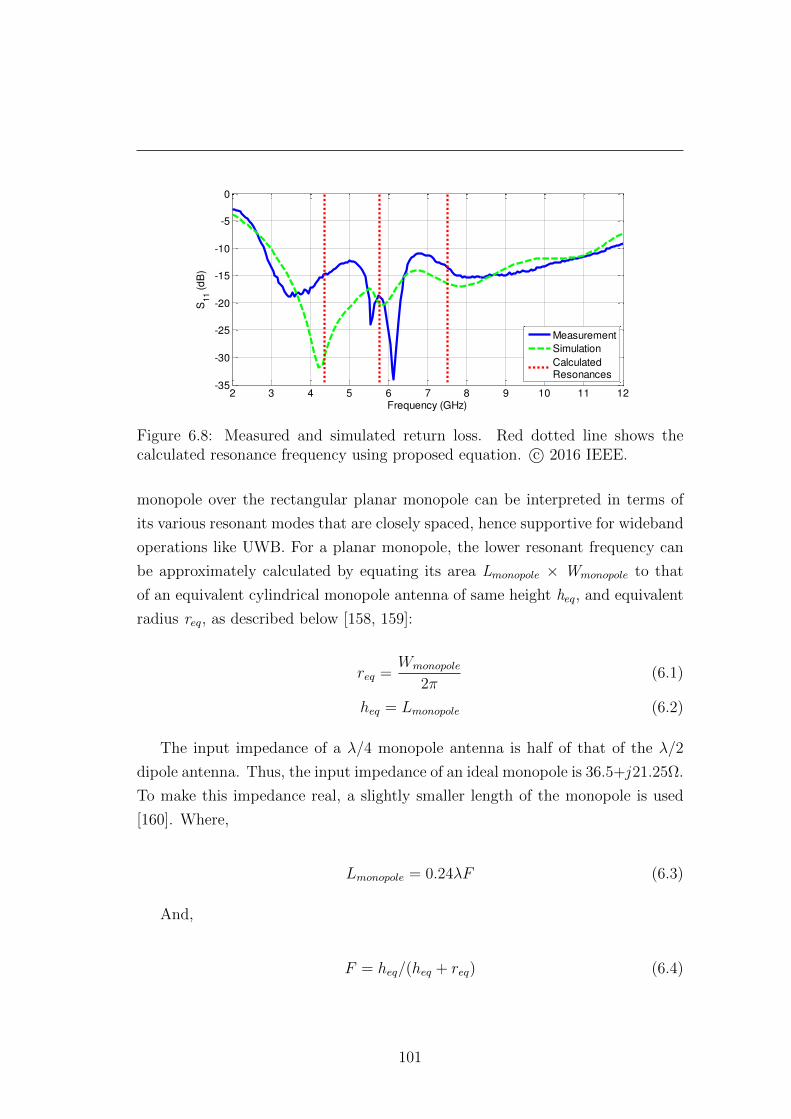
2 3 4 5 6 7 8 9 10 11 12-35
-30
-25
-20
-15
-10
-5
0
Frequency (GHz)
S11 (
dB
)
Measurement
Simulation
CalculatedResonances
Figure 6.8: Measured and simulated return loss. Red dotted line shows thecalculated resonance frequency using proposed equation. c© 2016 IEEE.
monopole over the rectangular planar monopole can be interpreted in terms of
its various resonant modes that are closely spaced, hence supportive for wideband
operations like UWB. For a planar monopole, the lower resonant frequency can
be approximately calculated by equating its area Lmonopole × Wmonopole to that
of an equivalent cylindrical monopole antenna of same height heq, and equivalent
radius req, as described below [158, 159]:
req =Wmonopole
2π(6.1)
heq = Lmonopole (6.2)
The input impedance of a λ/4 monopole antenna is half of that of the λ/2
dipole antenna. Thus, the input impedance of an ideal monopole is 36.5+j 21.25Ω.
To make this impedance real, a slightly smaller length of the monopole is used
[160]. Where,
Lmonopole = 0.24λF (6.3)
And,
F = heq/(heq + req) (6.4)
101
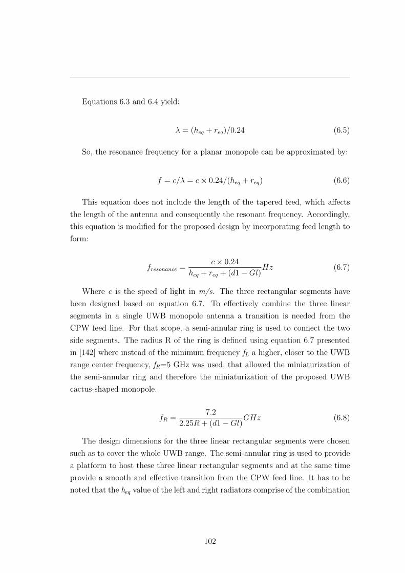
Equations 6.3 and 6.4 yield:
λ = (heq + req)/0.24 (6.5)
So, the resonance frequency for a planar monopole can be approximated by:
f = c/λ = c× 0.24/(heq + req) (6.6)
This equation does not include the length of the tapered feed, which affects
the length of the antenna and consequently the resonant frequency. Accordingly,
this equation is modified for the proposed design by incorporating feed length to
form:
fresonance =c× 0.24
heq + req + (d1−Gl)Hz (6.7)
Where c is the speed of light in m/s. The three rectangular segments have
been designed based on equation 6.7. To effectively combine the three linear
segments in a single UWB monopole antenna a transition is needed from the
CPW feed line. For that scope, a semi-annular ring is used to connect the two
side segments. The radius R of the ring is defined using equation 6.7 presented
in [142] where instead of the minimum frequency fL a higher, closer to the UWB
range center frequency, fR=5 GHz was used, that allowed the miniaturization of
the semi-annular ring and therefore the miniaturization of the proposed UWB
cactus-shaped monopole.
fR =7.2
2.25R + (d1−Gl)GHz (6.8)
The design dimensions for the three linear rectangular segments were chosen
such as to cover the whole UWB range. The semi-annular ring is used to provide
a platform to host these three linear rectangular segments and at the same time
provide a smooth and effective transition from the CPW feed line. It has to be
noted that the heq value of the left and right radiators comprise of the combination
102
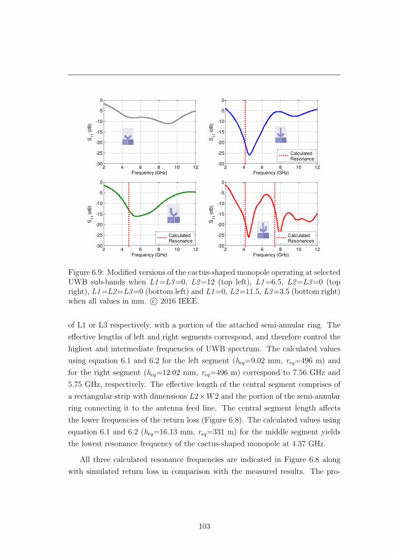
2 4 6 8 10 12-30
-25
-20
-15
-10
-5
0
Frequency (GHz)
S11 (
dB
)
2 4 6 8 10 12-30
-25
-20
-15
-10
-5
0
Frequency (GHz)
S11 (
dB
)
CalculatedResonance
2 4 6 8 10 12-30
-25
-20
-15
-10
-5
0
Frequency (GHz)
S11 (
dB
)
CalculatedResonance
2 4 6 8 10 12-30
-25
-20
-15
-10
-5
0
Frequency (GHz)
S11 (
dB
)
CalculatedResonances
Figure 6.9: Modified versions of the cactus-shaped monopole operating at selectedUWB sub-bands when L1 =L3 =0, L2 =12 (top left), L1 =6.5, L2 =L3 =0 (topright), L1 =L2 =L3 =0 (bottom left) and L1 =0, L2 =11.5, L3 =3.5 (bottom right)when all values in mm. c© 2016 IEEE.
of L1 or L3 respectively, with a portion of the attached semi-annular ring. The
effective lengths of left and right segments correspond, and therefore control the
highest and intermediate frequencies of UWB spectrum. The calculated values
using equation 6.1 and 6.2 for the left segment (heq=9.02 mm, req=496 m) and
for the right segment (heq=12.02 mm, req=496 m) correspond to 7.56 GHz and
5.75 GHz, respectively. The effective length of the central segment comprises of
a rectangular strip with dimensions L2×W2 and the portion of the semi-annular
ring connecting it to the antenna feed line. The central segment length affects
the lower frequencies of the return loss (Figure 6.8). The calculated values using
equation 6.1 and 6.2 (heq=16.13 mm, req=331 m) for the middle segment yields
the lowest resonance frequency of the cactus-shaped monopole at 4.37 GHz.
All three calculated resonance frequencies are indicated in Figure 6.8 along
with simulated return loss in comparison with the measured results. The pro-
103
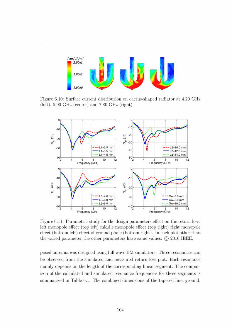
(a) (b) (c)
Fig. 4. Surface current distribution on cactus-shaped radiator at (a)
4.20 GHz, (b) 5.90 GHz and (c) 7.80 GHz
Jsurf [A/m]
2.00e1
1.00e1
1.00e0
2 4 6 8 10 12-40
-35
-30
-25
-20
-15
-10
-5
0
Frequency (GHz)
S11 (
dB
)
Calculated Resonances
UWB antenna S. K. Mishra, et al.
Figure 6.10: Surface current distribution on cactus-shaped radiator at 4.20 GHz(left), 5.90 GHz (center) and 7.80 GHz (right).
2 4 6 8 10 12-40
-30
-20
-10
0
Frequency (GHz)
S11 (
dB
)
L1=2.5 mm
L1=3.5 mm
L1=4.5 mm
2 4 6 8 10 12-50
-40
-30
-20
-10
0
Frequency (GHz)
S11 (
dB
)
L2=10.0 mm
L2=12.0 mm
L2=14.0 mm
2 4 6 8 10 12-40
-30
-20
-10
0
Frequency (GHz)
S11 (
dB
)
L3=4.0 mm
L3=6.0 mm
L3=8.0 mm
2 4 6 8 10 12-40
-30
-20
-10
0
Frequency (GHz)
S11 (
dB
)
Gw=6.0 mm
Gw=8.0 mm
Gw=10.0 mm
Figure 6.11: Parametric study for the design parameters effect on the return loss.left monopole effect (top left) middle monopole effect (top right) right monopoleeffect (bottom left) effect of ground plane (bottom right). In each plot other thanthe varied parameter the other parameters have same values. c© 2016 IEEE.
posed antenna was designed using full wave EM simulators. Three resonances can
be observed from the simulated and measured return loss plot. Each resonance
mainly depends on the length of the corresponding linear segment. The compar-
ison of the calculated and simulated resonance frequencies for these segments is
summarized in Table 6.1. The combined dimensions of the tapered line, ground,
104
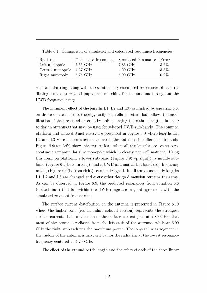
Table 6.1: Comparison of simulated and calculated resonance frequencies
Radiator Calculated fresonance Simulated fresonance ErrorLeft monopole 7.56 GHz 7.85 GHz 3.6%Central monopole 4.37 GHz 4.20 GHz 3.8%Right monopole 5.75 GHz 5.90 GHz 0.9%
semi-annular ring, along with the strategically calculated resonances of each ra-
diating stub, ensure good impedance matching for the antenna throughout the
UWB frequency range.
The imminent effect of the lengths L1, L2 and L3 -as implied by equation 6.6,
on the resonances of the, thereby, easily controllable return loss, allows the mod-
ification of the presented antenna by only changing these three lengths, in order
to design antennas that may be used for selected UWB sub-bands. The common
platform and three distinct cases, are presented in Figure 6.9 where lengths L1,
L2 and L3 were chosen such as to match the antennas in different sub-bands.
Figure 6.9(top left) shows the return loss, when all the lengths are set to zero,
creating a semi-annular ring monopole which in clearly not well matched. Using
this common platform, a lower sub-band (Figure 6.9(top right)), a middle sub-
band (Figure 6.9(bottom left)), and a UWB antenna with a band-stop frequency
notch, (Figure 6.9(bottom right)) can be designed. In all three cases only lengths
L1, L2 and L3 are changed and every other design dimension remains the same.
As can be observed in Figure 6.9, the predicted resonances from equation 6.6
(dotted lines) that fall within the UWB range are in good agreement with the
simulated resonant frequencies.
The surface current distribution on the antenna is presented in Figure 6.10
where the higher tone (red in online colored version) represents the strongest
surface current. It is obvious from the surface current plot at 7.80 GHz, that
most of the power is radiated from the left stub of the antenna, while at 5.90
GHz the right stub radiates the maximum power. The longest linear segment in
the middle of the antenna is most critical for the radiation at the lowest resonance
frequency centered at 4.20 GHz.
The effect of the ground patch length and the effect of each of the three linear
105
segments’ length, were parametrically studied, and the results are compiled in
Figure 6.11. The contour with the solid line in all four plots in Figure 6.11.
presents the optimized design’s simulation results. The width of the ground plane,
S2 directly affects the impedance matching at the lower frequencies, when S2 = 6
mm. Similar mismatch is observed at higher frequencies when S2 = 10 mm. The
optimized value of S2 is 8 mm, for which the antenna is matched everywhere in
the UWB band, as can be seen in Figure 6.11(top left). Figures 6.11(top right,
bottom right and bottom left) reveal the impact of each stub’s length on the
position of the respective resonance. In general, the increase in the length of a stub
causes the related resonance to shift towards lower frequencies. This tendency,
remains consistent as can be seen in every one of the three plots mentioned above.
The same behavior has been theoretically predicted from equation 6.6. One of
the most common issues in the resonances distribution approach, for wide band
antenna designs, is the ‘collapse of resonance’. This collapse often reveals a peak
in the return loss plot at the frequency band where the resonance previously
existed. This phenomenon can be observed in Figure 6.11(top right) for L1 =
4.5 mm. A similar mismatch problem is often observed when the two resonances
occur too far apart from each other. Such case can be witnessed in Figure 6.11(top
right) for L2=14 mm in which the first resonance shifts to lower frequencies,
resulting in a peak of return loss between the first two resonances. The most
intense mismatch peak can be observed from Figure 5(bottom left) when L3 =
4 mm. The reason behind this peak is the position of the second resonance far
away from the first resonance and its merge with the third resonance, eventually
resulting in significant mismatching of the |S11| around 6 GHz. The size of the
ground plane (S2) is an important parameter for the overall matching of the
antenna as it affects the position as well as the depth of each resonance. On the
other hand, the length of each stub does not significantly affect the depth or the
position of the resonances created by the other two stubs. It is evident that while
a certain stub only affects its corresponding resonance, the ground patches and
the cactus-shaped radiator should be considered as a single object, in order to
achieve good matching results throughout the complete UWB frequency range.
The design allows the interested designer to achieve good radiation perfor-
mance in different UWB sub-bands by only varying the lengths of the three
106
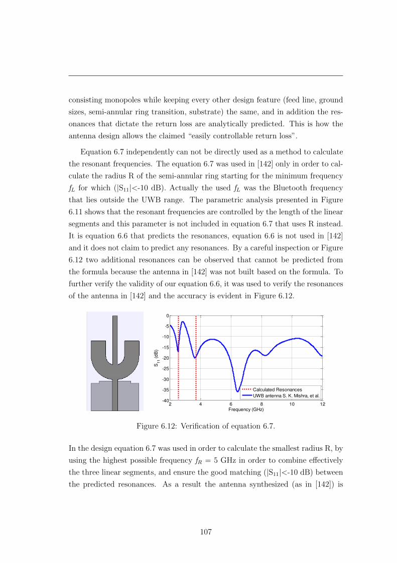
consisting monopoles while keeping every other design feature (feed line, ground
sizes, semi-annular ring transition, substrate) the same, and in addition the res-
onances that dictate the return loss are analytically predicted. This is how the
antenna design allows the claimed “easily controllable return loss”.
Equation 6.7 independently can not be directly used as a method to calculate
the resonant frequencies. The equation 6.7 was used in [142] only in order to cal-
culate the radius R of the semi-annular ring starting for the minimum frequency
fL for which (|S11|<-10 dB). Actually the used fL was the Bluetooth frequency
that lies outside the UWB range. The parametric analysis presented in Figure
6.11 shows that the resonant frequencies are controlled by the length of the linear
segments and this parameter is not included in equation 6.7 that uses R instead.
It is equation 6.6 that predicts the resonances, equation 6.6 is not used in [142]
and it does not claim to predict any resonances. By a careful inspection or Figure
6.12 two additional resonances can be observed that cannot be predicted from
the formula because the antenna in [142] was not built based on the formula. To
further verify the validity of our equation 6.6, it was used to verify the resonances
of the antenna in [142] and the accuracy is evident in Figure 6.12.
2 4 6 8 10 12-40
-35
-30
-25
-20
-15
-10
-5
0
Frequency (GHz)
S11 (
dB
)
Calculated Resonances
UWB antenna S. K. Mishra, et al.
Figure 6.12: Verification of equation 6.7.
In the design equation 6.7 was used in order to calculate the smallest radius R, by
using the highest possible frequency fR = 5 GHz in order to combine effectively
the three linear segments, and ensure the good matching (|S11|<-10 dB) between
the predicted resonances. As a result the antenna synthesized (as in [142]) is
107
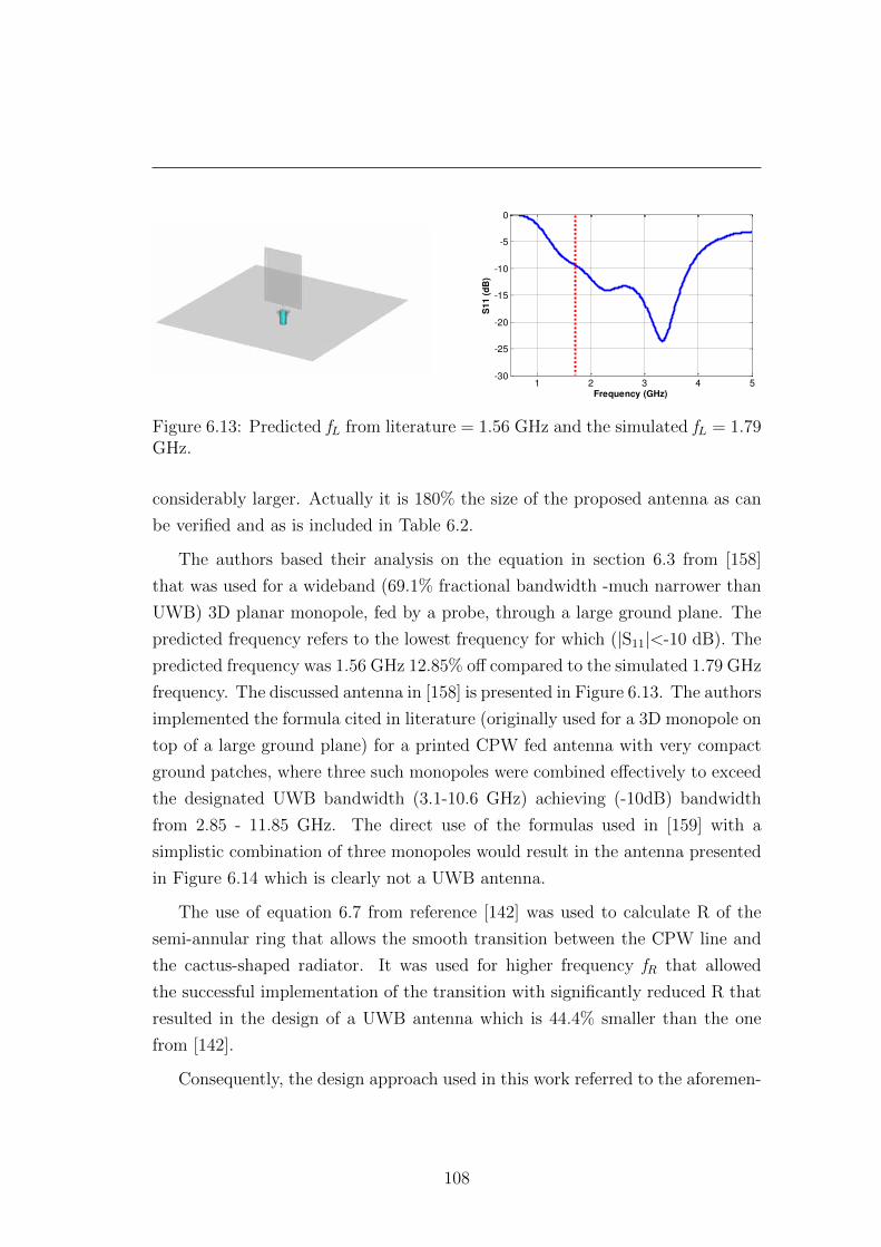
1 2 3 4 5-30
-25
-20
-15
-10
-5
0
Frequency (GHz)
S11 (
dB
)
Figure 6.13: Predicted fL from literature = 1.56 GHz and the simulated fL = 1.79GHz.
considerably larger. Actually it is 180% the size of the proposed antenna as can
be verified and as is included in Table 6.2.
The authors based their analysis on the equation in section 6.3 from [158]
that was used for a wideband (69.1% fractional bandwidth -much narrower than
UWB) 3D planar monopole, fed by a probe, through a large ground plane. The
predicted frequency refers to the lowest frequency for which (|S11|<-10 dB). The
predicted frequency was 1.56 GHz 12.85% off compared to the simulated 1.79 GHz
frequency. The discussed antenna in [158] is presented in Figure 6.13. The authors
implemented the formula cited in literature (originally used for a 3D monopole on
top of a large ground plane) for a printed CPW fed antenna with very compact
ground patches, where three such monopoles were combined effectively to exceed
the designated UWB bandwidth (3.1-10.6 GHz) achieving (-10dB) bandwidth
from 2.85 - 11.85 GHz. The direct use of the formulas used in [159] with a
simplistic combination of three monopoles would result in the antenna presented
in Figure 6.14 which is clearly not a UWB antenna.
The use of equation 6.7 from reference [142] was used to calculate R of the
semi-annular ring that allows the smooth transition between the CPW line and
the cactus-shaped radiator. It was used for higher frequency fR that allowed
the successful implementation of the transition with significantly reduced R that
resulted in the design of a UWB antenna which is 44.4% smaller than the one
from [142].
Consequently, the design approach used in this work referred to the aforemen-
108
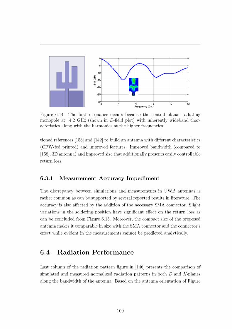
2 4 6 8 10 12-30
-25
-20
-15
-10
-5
0
Frequency (GHz)
S11 (
dB
)
Figure 6.14: The first resonance occurs because the central planar radiatingmonopole at 4.2 GHz (shown in E -field plot) with inherently wideband char-acteristics along with the harmonics at the higher frequencies.
tioned references [158] and [142] to build an antenna with different characteristics
(CPW-fed printed) and improved features. Improved bandwidth (compared to
[158], 3D antenna) and improved size that additionally presents easily controllable
return loss.
6.3.1 Measurement Accuracy Impediment
The discrepancy between simulations and measurements in UWB antennas is
rather common as can be supported by several reported results in literature. The
accuracy is also affected by the addition of the necessary SMA connector. Slight
variations in the soldering position have significant effect on the return loss as
can be concluded from Figure 6.15. Moreover, the compact size of the proposed
antenna makes it comparable in size with the SMA connector and the connector’s
effect while evident in the measurements cannot be predicted analytically.
6.4 Radiation Performance
Last column of the radiation pattern figure in [146] presents the comparison of
simulated and measured normalized radiation patterns in both E and H-planes
along the bandwidth of the antenna. Based on the antenna orientation of Figure
109
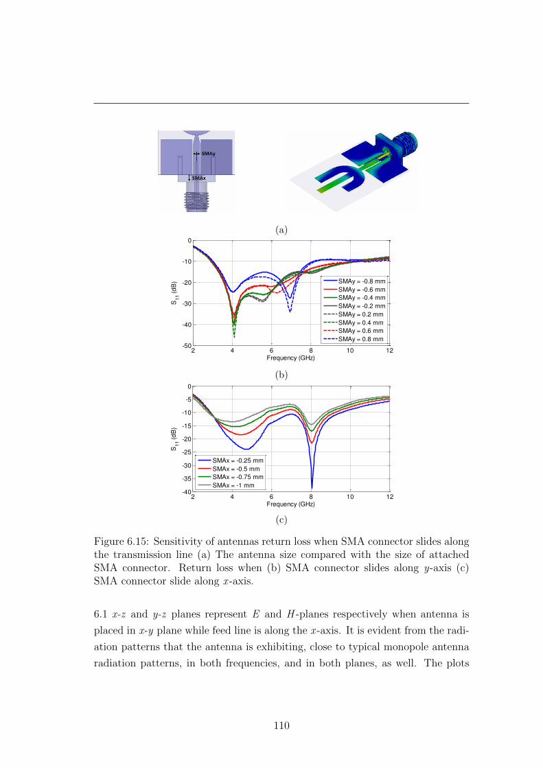
0 0
(a)
2 4 6 8 10 12-50
-40
-30
-20
-10
0
Frequency (GHz)
S11 (
dB
)
SMAy = -0.8 mm
SMAy = -0.6 mm
SMAy = -0.4 mm
SMAy = -0.2 mm
SMAy = 0.2 mm
SMAy = 0.4 mm
SMAy = 0.6 mm
SMAy = 0.8 mm
(b)
2 4 6 8 10 12-40
-35
-30
-25
-20
-15
-10
-5
0
Frequency (GHz)
S11 (
dB
)
SMAx = -0.25 mm
SMAx = -0.5 mm
SMAx = -0.75 mm
SMAx = -1 mm
(c)
Figure 6.15: Sensitivity of antennas return loss when SMA connector slides alongthe transmission line (a) The antenna size compared with the size of attachedSMA connector. Return loss when (b) SMA connector slides along y-axis (c)SMA connector slide along x -axis.
6.1 x-z and y-z planes represent E and H -planes respectively when antenna is
placed in x-y plane while feed line is along the x -axis. It is evident from the radi-
ation patterns that the antenna is exhibiting, close to typical monopole antenna
radiation patterns, in both frequencies, and in both planes, as well. The plots
110
also confirm the sustainability in radiation performance of the cactus-shaped an-
tenna throughout the UWB frequency range. Measured radiation patterns are in
good agreement with the simulated predictions, validating the performance of the
fabricated prototype. Although the antenna is not symmetrical, the presented
radiation patterns are almost symmetrical. The expected asymmetry in the ra-
diation patterns should be reflected on x-y plane cuts, however the measured
patterns are presented only in x-z and y-z planes. The primary parameters that
control the return loss (i,e, L1, L2 and L3) have minor effect on the antenna’s
radiation patterns which remain consistently omnidirectional along the H -plane.
The gain of the antenna is measured using the substitution method, in which a
2 to 18 GHz Q-par Angus Ltd rectangular horn antenna of known gain was used.
The gain accuracy of the horn antenna is within ±0.8 dB range, thus this can
be considered as the accuracy of the measurement setup for the cactus-shaped
antenna. A direct comparison of simulated and measured gain in complete UWB
frequency range is presented in Figure 6.7(c) Maximum gain is measured in φ =
θ = 0 i.e. in the direction of z -axis and the agreement between measurements
and simulated results is evident. The gain of the antenna grows linearly with
respect to frequency and the overall gain remains within 4 dB range. The very
consistent omnidirectional radiation patterns of the antenna, in H -plane, is the
reason that maximum gain is kept low as can be deduced from Table 6.2 that
provides a comparison between this work and the similar antennas reported in
the references. The consistent omni-directional patters in combination with the
compact size of the cactus-shaped monopole make the proposed antenna a good
candidate for most UWB applications.
6.5 Chapter Conclusions
Three proposed antennas in Section 6.1.1 are fabricated on flexible, low loss and
low cost LCP organic material and a miniaturization method is discussed. All
three antennas have a return loss better than -10 dB in the whole ultra-wideband
range and have close to omni-directional radiation patterns. The evolved cactus
antenna and miniaturized cactus antenna are developed based on the fact that the
111
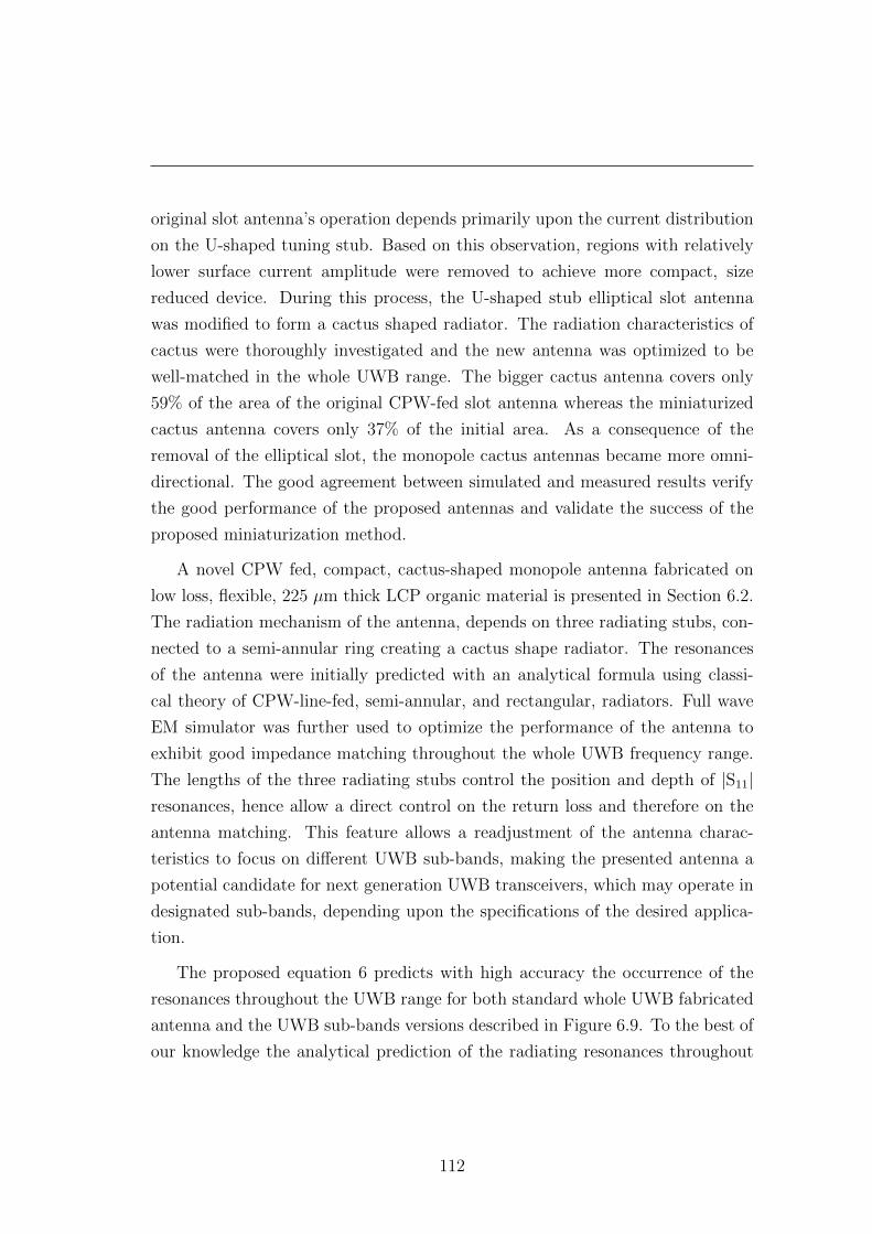
original slot antenna’s operation depends primarily upon the current distribution
on the U-shaped tuning stub. Based on this observation, regions with relatively
lower surface current amplitude were removed to achieve more compact, size
reduced device. During this process, the U-shaped stub elliptical slot antenna
was modified to form a cactus shaped radiator. The radiation characteristics of
cactus were thoroughly investigated and the new antenna was optimized to be
well-matched in the whole UWB range. The bigger cactus antenna covers only
59% of the area of the original CPW-fed slot antenna whereas the miniaturized
cactus antenna covers only 37% of the initial area. As a consequence of the
removal of the elliptical slot, the monopole cactus antennas became more omni-
directional. The good agreement between simulated and measured results verify
the good performance of the proposed antennas and validate the success of the
proposed miniaturization method.
A novel CPW fed, compact, cactus-shaped monopole antenna fabricated on
low loss, flexible, 225 µm thick LCP organic material is presented in Section 6.2.
The radiation mechanism of the antenna, depends on three radiating stubs, con-
nected to a semi-annular ring creating a cactus shape radiator. The resonances
of the antenna were initially predicted with an analytical formula using classi-
cal theory of CPW-line-fed, semi-annular, and rectangular, radiators. Full wave
EM simulator was further used to optimize the performance of the antenna to
exhibit good impedance matching throughout the whole UWB frequency range.
The lengths of the three radiating stubs control the position and depth of |S11|resonances, hence allow a direct control on the return loss and therefore on the
antenna matching. This feature allows a readjustment of the antenna charac-
teristics to focus on different UWB sub-bands, making the presented antenna a
potential candidate for next generation UWB transceivers, which may operate in
designated sub-bands, depending upon the specifications of the desired applica-
tion.
The proposed equation 6 predicts with high accuracy the occurrence of the
resonances throughout the UWB range for both standard whole UWB fabricated
antenna and the UWB sub-bands versions described in Figure 6.9. To the best of
our knowledge the analytical prediction of the radiating resonances throughout
112
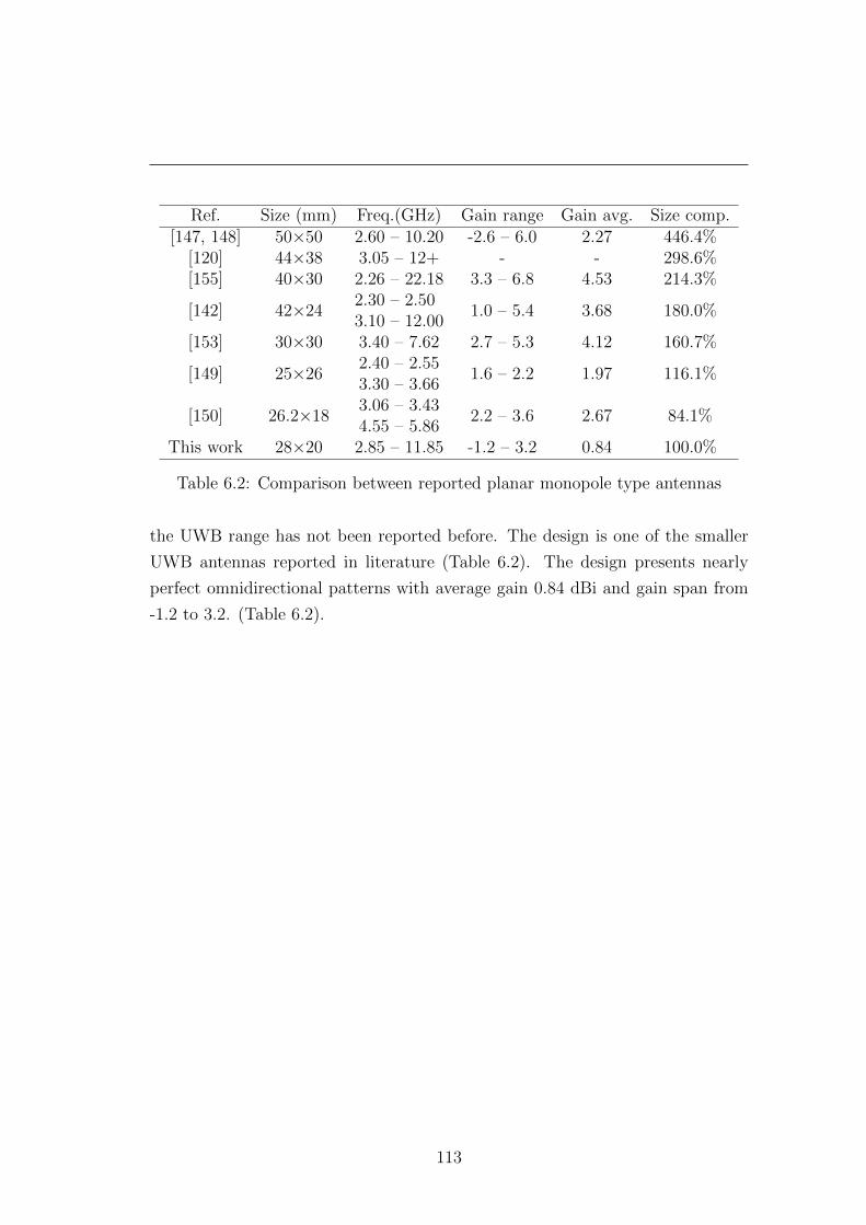
Ref. Size (mm) Freq.(GHz) Gain range Gain avg. Size comp.[147, 148] 50×50 2.60 – 10.20 -2.6 – 6.0 2.27 446.4%
[120] 44×38 3.05 – 12+ - - 298.6%[155] 40×30 2.26 – 22.18 3.3 – 6.8 4.53 214.3%
[142] 42×242.30 – 2.503.10 – 12.00
1.0 – 5.4 3.68 180.0%
[153] 30×30 3.40 – 7.62 2.7 – 5.3 4.12 160.7%
[149] 25×262.40 – 2.553.30 – 3.66
1.6 – 2.2 1.97 116.1%
[150] 26.2×183.06 – 3.434.55 – 5.86
2.2 – 3.6 2.67 84.1%
This work 28×20 2.85 – 11.85 -1.2 – 3.2 0.84 100.0%
Table 6.2: Comparison between reported planar monopole type antennas
the UWB range has not been reported before. The design is one of the smaller
UWB antennas reported in literature (Table 6.2). The design presents nearly
perfect omnidirectional patterns with average gain 0.84 dBi and gain span from
-1.2 to 3.2. (Table 6.2).
113
Appendix A
Efficient Rectifiers for Wireless
Power Transfer
The rectifier design approach for the implementation of a System on Package
(SOP) Wireless Power Transfer (WPT) receiver is discussed. Real Wireless Power
Transfer testing conditions revolved around the rectifier component. For the
WPT receiver module, the 1.6 GHz rectifier operated with a 49% RF-to-DC
efficiency for an input RF power of -10 dBm. Three efficient rectifiers, first at
2.45 GHz ISM band, second at higher frequency (5.6 GHz), and third at lower
frequency (1.6 GHz) is presented.
A.1 Introduction and Background
Wireless energy transfer has been studied for decades now since it dates back to
the experiments of Heinrich Hertz. Shifting to a much more recent decade, this
research topic gained a lot of attention indirectly when radio frequency identifica-
tion (RFID) applications surfaced in day-to-day applications. RFID systems were
initially introduced in the late 1990’s for very short range systems (< 1.5 meters)
operating at either 0.9 GHz or at 2.4 GHz, ISM band, and were used for industrial
applications. However, it is with the rapid development of the Internet of Things
(IoT) devices,- that took place mostly in the last five years,- that increased at-
114
tention was paid in wireless charging in an attempt to spare the battery and thus
reduce the overall cost and the maintenance cost of such wireless nodes. The
rectenna design, and more specifically the RF-to-DC efficiency of the rectifier has
been the key focus of the related research with ultimate scope the implementa-
tion of efficient Wireless Power Transmission (WPT) systems. It has been noted
that for low RF input power levels, the RF-to-DC efficiency of most rectifiers
is normally very low. Therefore, most of the research effort, straightforwardly,
aimed the intensification of the rectifier’s efficiency. Some very recent approaches
are presented in literature, like balanced rectifiers [161, 162] that compensate the
microwave circuits terminations to recycle the resistive dissipated power, based
on single [163], dual [164], multiple diodes [162], and even system in package
(SiP) [165] low-loss, integrated, passive devices. In this approach, the impedance
matching at the rectifier’s input and output terminals with the antenna and the
power management unit (PMU) respectively has always been the major bottle-
neck in the overall performance. The obvious choice of wide impedance matching
network has been known to severely deteriorate the RF-to-DC efficiency for a
wide range of input power levels. Some recent studies, [166, 167] have focused
mostly on possible solutions to this very specific and seemingly simple problem.
The high importance of the matching problem at the input and output terminals
of a rectifier is the reason why in this paper the key system elements of rectifiers
are not studied only as standalone devices but they are also studied as part of
a rectenna (antenna + rectifier module) and as part of a complete system with
a DC-to-DC booster connected on the output of the rectifier. In addition to the
matching problem, most rectifier topologies have evidently different behavior for
different frequencies. In general, higher frequency rectifiers normally incur lower
efficiency, and consequently charge pump topologies with the class-F loads [168],
boost converter [169], buck-boost [170] etc. are used to enhance the harvested
energy at DC level. In all the aforementioned topologies, rectifiers’ operation and
their RF-to-DC efficiency has been demonstrated to be the key feature for the
WPT receiver. Even mathematical models like [171] have been proposed to pin-
point the highest possible RF-to-DC efficiency at a given power level, frequency
and output load. It has been reported in literature that there is always a trade-off
between complexity, cost, operational power level and the frequency of a rectifier.
115
In this chapter the voltage double topology [172] has been preferred for the
rectifier designs and fabricated rectifiers at three different frequencies are pre-
sented.
A.2 Rectifier Design
There are different RF-to-DC rectifier topologies to choose from depending on
the application’s specifications. The most popular topology is the voltage doubler
that consists of two Schottky diodes and two capacitors therefore this is the only
type of rectifier considered in this work as shown in Figure A.1. Voltage doubler
has a fairly simple topology, can have a relatively compact size, and is preferred
when high efficiency can be traded. It has been demonstrated that the number
of rectification ladders have a direct relation with rectifier efficiency, however
losses increase too [171]. When a rectifier is intended for energy harvesting, as
a component of a WPT system receiver, the most important feature is the RF-
to-DC efficiency which needs to be as high as possible. However, rectifiers are
non-linear circuits and practically this means that their efficiency depends non-
linearly on a) the input RF power, and b) the termination load. Generally, a
rectifier should have high RF-to-DC efficiency for a wide range of input power
levels and similarly high efficiency, for a wide range of termination loads, since the
subsequent to the rectifier component, which is usually a power management unit,
(PMU), has a varying input impedance that depends on its unforeseen operation
conditions at the time.
A.2.1 2.45 GHz Rectifier
The rectifier was designed at 2.45 GHz keeping in mind its potential use for
wireless power transfer in Wireless Body Area Network (WBAN) applications.
Keysight Advanced Design System (ADS) was used to design the hosting traces
of the rectifiers commercially available lumped components. Lumped components
were simulated using the vendors ADS library models, and 0.787 mm thick Rogers
RT/duroid 5880 substrate was used with εr = 2.2, tanδ = 0.0009. In order to
116
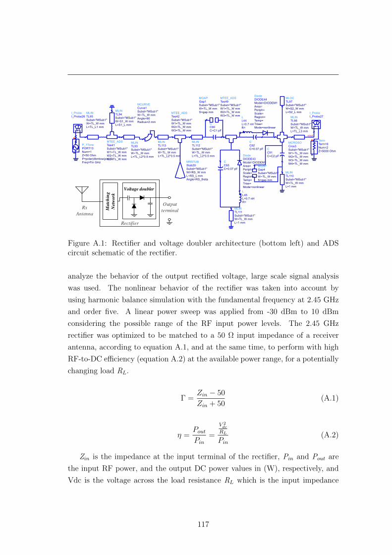
Matc
hin
g
Net
work
Rx
Antenna
Rectifier
Output
terminal
Voltage doubler
Figure A.1: Rectifier and voltage doubler architecture (bottom left) and ADScircuit schematic of the rectifier.
analyze the behavior of the output rectified voltage, large scale signal analysis
was used. The nonlinear behavior of the rectifier was taken into account by
using harmonic balance simulation with the fundamental frequency at 2.45 GHz
and order five. A linear power sweep was applied from -30 dBm to 10 dBm
considering the possible range of the RF input power levels. The 2.45 GHz
rectifier was optimized to be matched to a 50 Ω input impedance of a receiver
antenna, according to equation A.1, and at the same time, to perform with high
RF-to-DC efficiency (equation A.2) at the available power range, for a potentially
changing load RL.
Γ =Zin − 50
Zin + 50(A.1)
η =PoutPin
=
V 2dc
RL
Pin(A.2)
Zin is the impedance at the input terminal of the rectifier, Pin and Pout are
the input RF power, and the output DC power values in (W), respectively, and
Vdc is the voltage across the load resistance RL which is the input impedance
117
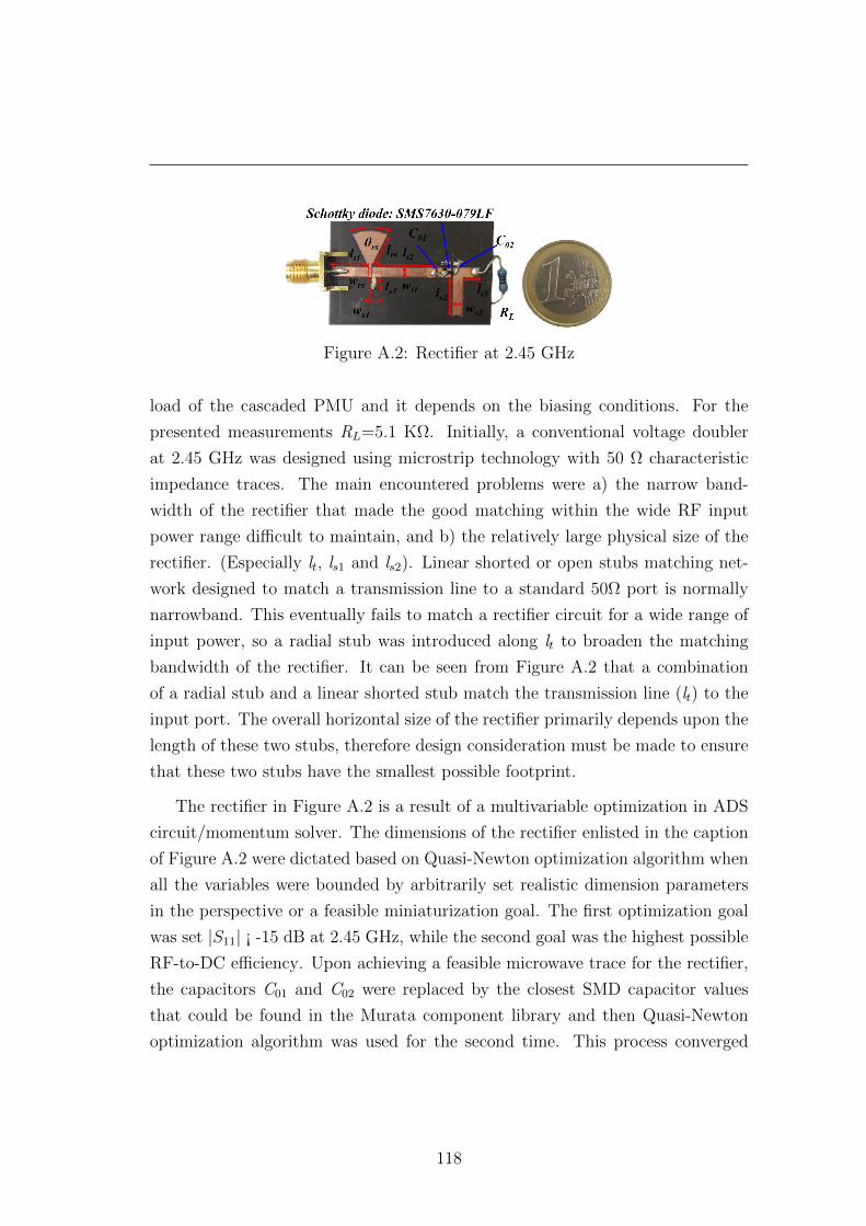
Figure A.2: Rectifier at 2.45 GHz
load of the cascaded PMU and it depends on the biasing conditions. For the
presented measurements RL=5.1 KΩ. Initially, a conventional voltage doubler
at 2.45 GHz was designed using microstrip technology with 50 Ω characteristic
impedance traces. The main encountered problems were a) the narrow band-
width of the rectifier that made the good matching within the wide RF input
power range difficult to maintain, and b) the relatively large physical size of the
rectifier. (Especially lt, ls1 and ls2). Linear shorted or open stubs matching net-
work designed to match a transmission line to a standard 50Ω port is normally
narrowband. This eventually fails to match a rectifier circuit for a wide range of
input power, so a radial stub was introduced along lt to broaden the matching
bandwidth of the rectifier. It can be seen from Figure A.2 that a combination
of a radial stub and a linear shorted stub match the transmission line (lt) to the
input port. The overall horizontal size of the rectifier primarily depends upon the
length of these two stubs, therefore design consideration must be made to ensure
that these two stubs have the smallest possible footprint.
The rectifier in Figure A.2 is a result of a multivariable optimization in ADS
circuit/momentum solver. The dimensions of the rectifier enlisted in the caption
of Figure A.2 were dictated based on Quasi-Newton optimization algorithm when
all the variables were bounded by arbitrarily set realistic dimension parameters
in the perspective or a feasible miniaturization goal. The first optimization goal
was set |S11| ¡ -15 dB at 2.45 GHz, while the second goal was the highest possible
RF-to-DC efficiency. Upon achieving a feasible microwave trace for the rectifier,
the capacitors C01 and C02 were replaced by the closest SMD capacitor values
that could be found in the Murata component library and then Quasi-Newton
optimization algorithm was used for the second time. This process converged
118
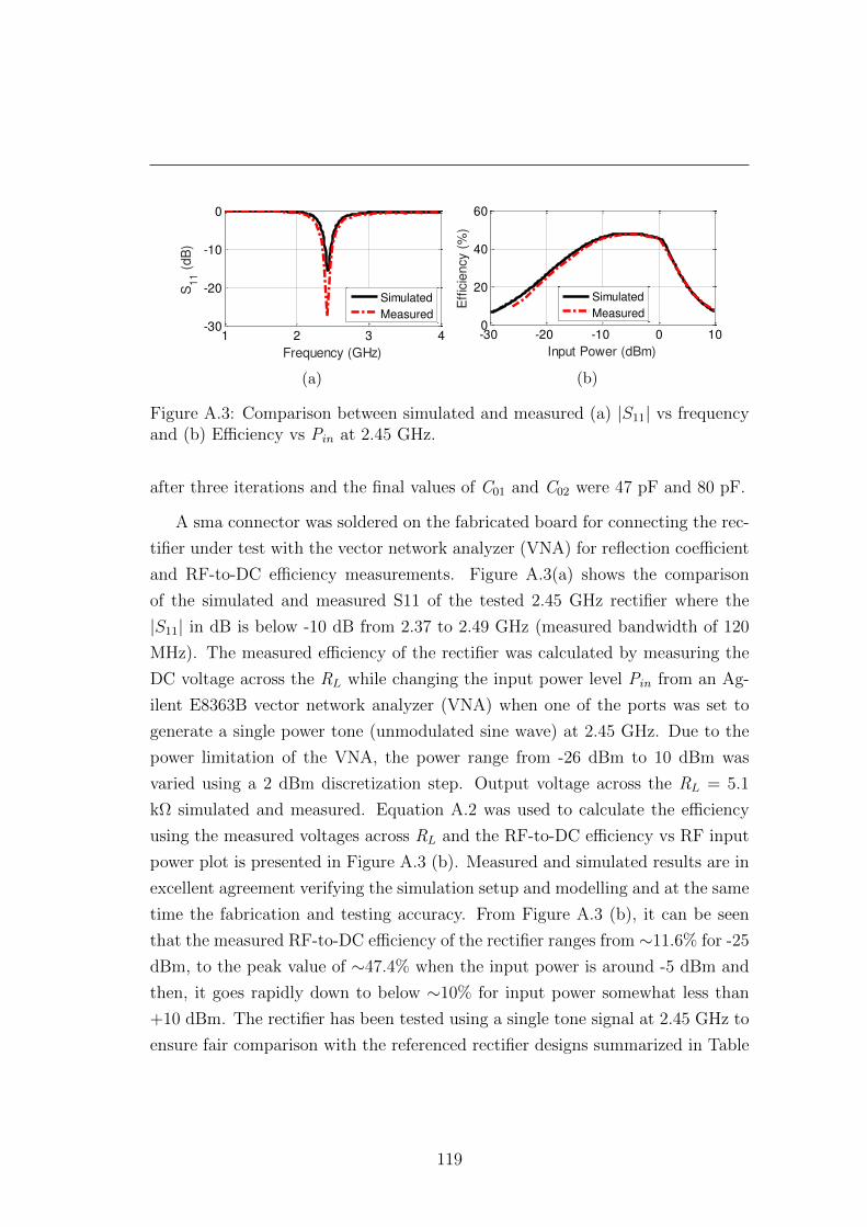
1 2 3 4-30
-20
-10
0
Frequency (GHz)
S1
1 (
dB
)
Simulated
Measured
(a)
-30 -20 -10 0 100
20
40
60
Input Power (dBm)
Eff
icie
ncy (
%)
Simulated
Measured
(b)
Figure A.3: Comparison between simulated and measured (a) |S11| vs frequencyand (b) Efficiency vs Pin at 2.45 GHz.
after three iterations and the final values of C01 and C02 were 47 pF and 80 pF.
A sma connector was soldered on the fabricated board for connecting the rec-
tifier under test with the vector network analyzer (VNA) for reflection coefficient
and RF-to-DC efficiency measurements. Figure A.3(a) shows the comparison
of the simulated and measured S11 of the tested 2.45 GHz rectifier where the
|S11| in dB is below -10 dB from 2.37 to 2.49 GHz (measured bandwidth of 120
MHz). The measured efficiency of the rectifier was calculated by measuring the
DC voltage across the RL while changing the input power level Pin from an Ag-
ilent E8363B vector network analyzer (VNA) when one of the ports was set to
generate a single power tone (unmodulated sine wave) at 2.45 GHz. Due to the
power limitation of the VNA, the power range from -26 dBm to 10 dBm was
varied using a 2 dBm discretization step. Output voltage across the RL = 5.1
kΩ simulated and measured. Equation A.2 was used to calculate the efficiency
using the measured voltages across RL and the RF-to-DC efficiency vs RF input
power plot is presented in Figure A.3 (b). Measured and simulated results are in
excellent agreement verifying the simulation setup and modelling and at the same
time the fabrication and testing accuracy. From Figure A.3 (b), it can be seen
that the measured RF-to-DC efficiency of the rectifier ranges from ∼11.6% for -25
dBm, to the peak value of ∼47.4% when the input power is around -5 dBm and
then, it goes rapidly down to below ∼10% for input power somewhat less than
+10 dBm. The rectifier has been tested using a single tone signal at 2.45 GHz to
ensure fair comparison with the referenced rectifier designs summarized in Table
119
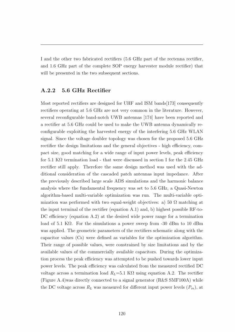
I and the other two fabricated rectifiers (5.6 GHz part of the rectenna rectifier,
and 1.6 GHz part of the complete SOP energy harvester module rectifier) that
will be presented in the two subsequent sections.
A.2.2 5.6 GHz Rectifier
Most reported rectifiers are designed for UHF and ISM bands[173] consequently
rectifiers operating at 5.6 GHz are not very common in the literature. However,
several reconfigurable band-notch UWB antennas [174] have been reported and
a rectifier at 5.6 GHz could be used to make the UWB antenna dynamically re-
configurable exploiting the harvested energy of the interfering 5.6 GHz WLAN
signal. Since the voltage doubler topology was chosen for the proposed 5.6 GHz
rectifier the design limitations and the general objectives - high efficiency, com-
pact size, good matching for a wide range of input power levels, peak efficiency
for 5.1 KΩ termination load - that were discussed in section I for the 2.45 GHz
rectifier still apply. Therefore the same design method was used with the ad-
ditional consideration of the cascaded patch antennas input impedance. After
the previously described large scale ADS simulations and the harmonic balance
analysis where the fundamental frequency was set to 5.6 GHz, a Quasi-Newton
algorithm-based multi-variable optimization was run. The multi-variable opti-
mization was performed with two equal-weight objectives: a) 50 Ω matching at
the input terminal of the rectifier (equation A.1) and, b) highest possible RF-to-
DC efficiency (equation A.2) at the desired wide power range for a termination
load of 5.1 KΩ. For the simulations a power sweep from -30 dBm to 10 dBm
was applied. The geometric parameters of the rectifiers schematic along with the
capacitor values (Cs) were defined as variables for the optimization algorithm.
Their range of possible values, were constrained by size limitations and by the
available values of the commercially available capacitors. During the optimiza-
tion process the peak efficiency was attempted to be pushed towards lower input
power levels. The peak efficiency was calculated from the measured rectified DC
voltage across a termination load RL=5.1 KΩ using equation A.2. The rectifier
(Figure A.4)was directly connected to a signal generator (R&S SMF100A) while
the DC voltage across RL was measured for different input power levels (Pin), at
120
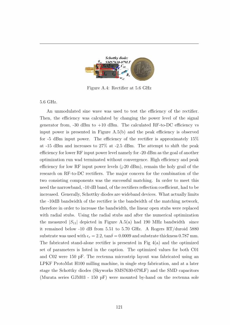
Figure A.4: Rectifier at 5.6 GHz
5.6 GHz.
An unmodulated sine wave was used to test the efficiency of the rectifier.
Then, the efficiency was calculated by changing the power level of the signal
generator from, -30 dBm to +10 dBm. The calculated RF-to-DC efficiency vs
input power is presented in Figure A.5(b) and the peak efficiency is observed
for -5 dBm input power. The efficiency of the rectifier is approximately 15%
at -15 dBm and increases to 27% at -2.5 dBm. The attempt to shift the peak
efficiency for lower RF input power level namely for -20 dBm as the goal of another
optimization run wad terminated without convergence. High efficiency and peak
efficiency for low RF input power levels (¡-20 dBm), remain the holy grail of the
research on RF-to-DC rectifiers. The major concern for the combination of the
two consisting components was the successful matching. In order to meet this
need the narrowband, -10 dB band, of the rectifiers reflection coefficient, had to be
increased. Generally, Schottky diodes are wideband devices. What actually limits
the -10dB bandwidth of the rectifier is the bandwidth of the matching network,
therefore in order to increase the bandwidth, the linear open stubs were replaced
with radial stubs. Using the radial stubs and after the numerical optimization
the measured |S11| depicted in Figure A.5(a) had 190 MHz bandwidth since
it remained below -10 dB from 5.51 to 5.70 GHz. A Rogers RT/duroid 5880
substrate was used with εr = 2.2, tanδ = 0.0009 and substrate thickness 0.787 mm.
The fabricated stand-alone rectifier is presented in Fig 4(a) and the optimized
set of parameters is listed in the caption. The optimized values for both C01
and C02 were 150 pF. The rectenna microstrip layout was fabricated using an
LPKF ProtoMat H100 milling machine, in single step fabrication, and at a later
stage the Schottky diodes (Skyworks SMS7630-079LF) and the SMD capacitors
(Murata series GJM03 - 150 pF) were mounted by-hand on the rectenna sole
121
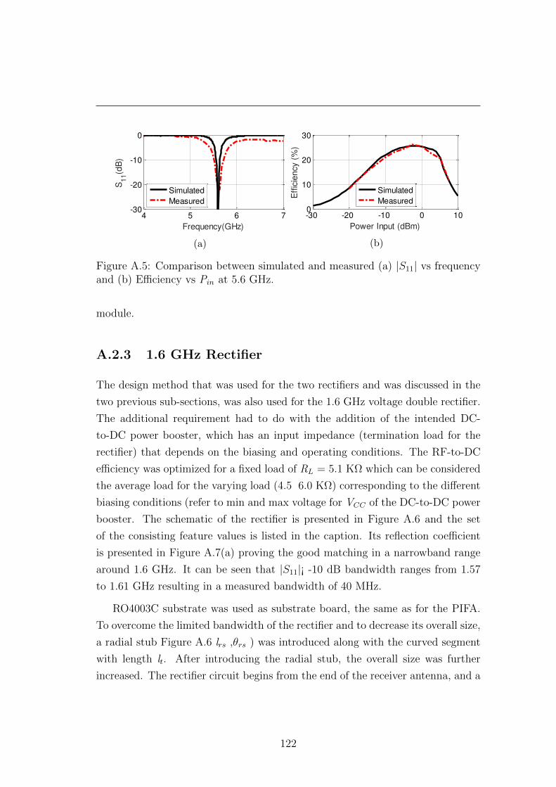
4 5 6 7-30
-20
-10
0
Frequency(GHz)
S1
1(d
B)
Simulated
Measured
(a)
-30 -20 -10 0 100
10
20
30
Power Input (dBm)
Eff
icie
ncy (
%)
Simulated
Measured
(b)
Figure A.5: Comparison between simulated and measured (a) |S11| vs frequencyand (b) Efficiency vs Pin at 5.6 GHz.
module.
A.2.3 1.6 GHz Rectifier
The design method that was used for the two rectifiers and was discussed in the
two previous sub-sections, was also used for the 1.6 GHz voltage double rectifier.
The additional requirement had to do with the addition of the intended DC-
to-DC power booster, which has an input impedance (termination load for the
rectifier) that depends on the biasing and operating conditions. The RF-to-DC
efficiency was optimized for a fixed load of RL = 5.1 KΩ which can be considered
the average load for the varying load (4.5 6.0 KΩ) corresponding to the different
biasing conditions (refer to min and max voltage for VCC of the DC-to-DC power
booster. The schematic of the rectifier is presented in Figure A.6 and the set
of the consisting feature values is listed in the caption. Its reflection coefficient
is presented in Figure A.7(a) proving the good matching in a narrowband range
around 1.6 GHz. It can be seen that |S11|¡ -10 dB bandwidth ranges from 1.57
to 1.61 GHz resulting in a measured bandwidth of 40 MHz.
RO4003C substrate was used as substrate board, the same as for the PIFA.
To overcome the limited bandwidth of the rectifier and to decrease its overall size,
a radial stub Figure A.6 lrs ,θrs ) was introduced along with the curved segment
with length lt. After introducing the radial stub, the overall size was further
increased. The rectifier circuit begins from the end of the receiver antenna, and a
122
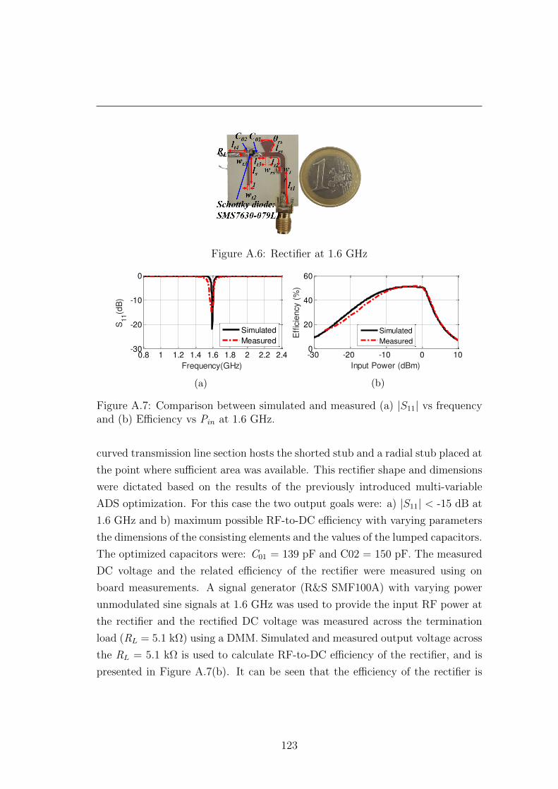
Figure A.6: Rectifier at 1.6 GHz
0.8 1 1.2 1.4 1.6 1.8 2 2.2 2.4-30
-20
-10
0
Frequency(GHz)
S1
1(d
B)
Simulated
Measured
(a)
-30 -20 -10 0 100
20
40
60
Input Power (dBm)
Eff
icie
ncy (
%)
Simulated
Measured
(b)
Figure A.7: Comparison between simulated and measured (a) |S11| vs frequencyand (b) Efficiency vs Pin at 1.6 GHz.
curved transmission line section hosts the shorted stub and a radial stub placed at
the point where sufficient area was available. This rectifier shape and dimensions
were dictated based on the results of the previously introduced multi-variable
ADS optimization. For this case the two output goals were: a) |S11| < -15 dB at
1.6 GHz and b) maximum possible RF-to-DC efficiency with varying parameters
the dimensions of the consisting elements and the values of the lumped capacitors.
The optimized capacitors were: C01 = 139 pF and C02 = 150 pF. The measured
DC voltage and the related efficiency of the rectifier were measured using on
board measurements. A signal generator (R&S SMF100A) with varying power
unmodulated sine signals at 1.6 GHz was used to provide the input RF power at
the rectifier and the rectified DC voltage was measured across the termination
load (RL = 5.1 kΩ) using a DMM. Simulated and measured output voltage across
the RL = 5.1 kΩ is used to calculate RF-to-DC efficiency of the rectifier, and is
presented in Figure A.7(b). It can be seen that the efficiency of the rectifier is
123

∼20% and goes up to ∼49% when the input power level increases from -25 dBm
to -10 dBm.
124

Appendix B
List of Publications
A portion of this thesis is published in parts. It is to declare that the author
already completed the copy rights transfer for the papers already in press. An
accurate acknowledgment of the papers should be made with given Digital Object
Identifiers (DOI) while citing the relevant portion of this thesis. Personal use
of this material is permitted. Permission from publisher must be obtained for
all other uses, in any current or future media, including reprinting/republishing
this material for advertising or promotional purposes, creating new collective
works, for resale or redistribution to servers or lists, or reuse of any copyrighted
component of this work in other works.
Journal papers in press:
1. M. Ali Babar Abbasi, S. Nikolaou, Marco Antoniades, M. N. Stevanovic,
P. Vryonides, “Compact EBG-Backed Planar Monopole for BAN Wearable
Applications,” IEEE Transactions on Antennas and Propagation, Vol.65,
Iss. 2, pp.1 - 11, February 2017. DOI: 10.1109/TAP.2016.2635588
2. M. Ali Babar Abbasi, Marco A. Antoniades and S. Nikolaou, , “A
Compact Reconfigurable NRI- TL Metamaterial PhaseShifter for Antenna
Applications” IEEE Transactions on Antennas and Propagation, 2017 (ac-
cepted for publication). DOI: 10.1109/TAP.2017.2777520
125

3. S. Nikolaou, M. Ali Babar Abbasi, “Design and Development of a Com-
pact UWB Monopole Antenna with Easily-Controllable Return Loss” IEEE
Transactions on Antennas and Propagation, Vol.65, Iss. 4, pp.1 - 5, April
2017. DOI: 10.1109/TAP.2017.2670322
4. Symeon Nikolaou, Muhammad Ali Babar Abbasi, “Miniaturization of
UWB Antennas on Organic Material,” International Journal of Antennas
and Propagation (IJAP), vol. 16, 2016. DOI: 10.1155/2016/5949254
5. S. Arain, Photos Vryonides, M. Ali Babar Abbasi, A. Quddious, Marco
A. Antoniades and S. Nikolaou, “Reconfigurable Bandwidth Bandpass Fil-
ter with Enhanced out-of-band Rejection Using π-Section-Loaded Ring Res-
onator”, IEEE Microwave and Wireless Components Letters, vol. 28, no.
1, pp. 28-30, Jan. 2018. DOI: 10.1109/LMWC.2017.2776212
6. S. Arain, Photos Vryonides, M. Ali Babar Abbasi, A. Quddious, Marco
A. Antoniades and S. Nikolaou, Wideband BPF Using Quadruple-Mode
Ring Resonator Loaded with Short-Circuited Stubs and Γ-Shaped Band-
Stop Sections, Wiley Microwave and Optical Technology Letters (MOTL),
, 59(9), pp. 2316-2320, 2017. DOI: 10.1002/mop.30737
7. S. Arain, Photos Vryonides, M. Ali Babar Abbasi, A. Quddious, Marco
A. Antoniades and S. Nikolaou, On the Use of Tunable Power Splitter for
Simultaneous Wireless Information and Power Transfer Receivers, Interna-
tional Journal of Antennas and Propagation, vol. 2018, Article ID 6183412,
12 pages, 2018. DOI: 10.1155/2018/6183412
Conference papers in press:
7. Muhammad Ali Babar Abbasi, Abdul Quddious, Marco Antoniades,
Symeon Nikolaou, “Wearable sensor for communication with implantable
devices,” submitted in 12th European Conference on Antennas and Propa-
gation (EuCAP), London, 2018.
8. M. A. Antoniades, M. A. B. Abbasi, M. Nikolic, P. Vryonides and S.
Nikolaou, “Conformal wearable monopole antenna backed by a compact
126
EBG structure for body area networks,” 2017 11th European Conference
on Antennas and Propagation (EUCAP), Paris, 2017, pp. 164-166.
9. M. A. B. Abbasi, S. Nikolaou and M. A. Antoniades, “A high gain EBG
backed monopole for MBAN off-body communication,” IEEE International
Symposium on Antennas and Propagation (APSURSI), Fajardo, PR, USA,
pp. 1907-1908, 2016.
10. S. Arain, M. A. B. Abassi, S. Nikolaou and P. Vryonides, “A square ring
resonator bandpass filter with asymmetrically loaded open circuited stubs,”
5th International Conference on Modern Circuits and Systems Technologies
(MOCAST), Thessaloniki, Greece, pp. 1-4, 2016.
11. M. A. B. Abbasi, P. Vryonides and S. Nikolaou, “Humidity sensor de-
vices using PEDOT:PSS,” IEEE International Symposium on Antennas and
Propagation & USNC/URSI National Radio Science Meeting, Vancouver,
BC, 2015, pp. 1366-1367.
12. M. Ali Babar Abbasi, D. Philippou, and S. Nikolaou, “Comparison
Study of Layered Homogeneous Models with Detailed Human Tissue Models
for Through-body Communications”, Progress in Electromagnetic Research
Symposium (PIERS), Prague, Czech Republic, 2015.
13. M. Ali Babar Abbasi, S. Arain, P. Vryonides, and S. Nikolaou, “De-
sign and optimization of miniaturized dual-band implantable antenna for
MICS and ISM bands” Progress in Electromagnetic Research Symposium
(PIERS), Prague, Czech Republic, 2015.
14. S. Arain, M. Ali Babar Abbasi, S. Nikolaou, and P. Vryonides, “A Re-
configurable Bandpass to Bandstop Filter Using PIN Diodes Based on the
Square Ring Resonator”, Progress in Electromagnetic Research Symposium,
Prague (PIERS), Prague, Czech Republic, 2015.
Forthcoming:
127

15. Muhammad Ali Babar Abbasi, Abdul Quddious, Aqeela Saghir, Salman
Arain, Marco A. Antoniades, Photos Vryonides, Symeon Nikolaou, Dynam-
ically Reconfigurable Single- to Dual-Band SIR Filter, awaited to be sub-
mitted in IEEE Transactions on Microwave Theory and Techniques, 2017.
16. Muhammad Ali Babar Abbasi, Marco A. Antoniades, Nikolaou Com-
pact NRI-TL Metamaterial Microstrip Crossover, submitted in IET Elec-
tronics Letters, 2017.
17. Abdul Quddious, M. Ali Babar Abbasi, Farooq A. Tahir, Marco A. An-
toniades, Photos Vryonides, Symeon Nikolaou, “UWB Antenna with Dy-
namically Reconfigurable Notch-Band,” submitted in IEEE Transactions
on Antennas and Propagation, 2017.
18. H. Nawaz, S. Sadiq, M. A. B. Abbasi and S. Nikolaou, Mutual Coupling
Reduction between Finite Spaced Planar Antenna Elements using Modified
Ground Structure, submitted in Wiley Microwave and Optical Technology
Letters (MOTL), 2017.
19. Abdul Quddious, Muhammad Ali Babar Abbasi, Haroon Tariq Awan,
Photos Vryonides, Alexis Polycarpou, M.A. Antoniades, Symeon Nikolaou1
“On the Design and Implementation of a System on Package (SOP) Receiver
for Wireless Power Transmission Applications”, to be submitted in IET
Microwaves, Antennas & Propagation, 2017.
20. Muhammad Sufian Anwar, Symeon Nikolaou, Hamza Nawaz and M. Ali
Babar Abbasi, Synthesis of Cross-Coupled Trisection and Quadruplet
Bandpass Filters Using Hybrid Structures of λ/4 and λ/2 Resonators, sub-
mitted in IEEE Transactions on Microwave Theory and Techniques, 2017.
21. S. Arain, Photos Vryonides, A. Quddious, M. Ali Babar Abbasi, Marco
A. Antoniades and S. Nikolaou, “Square Ring Resonator Based Switchable
Bandpass-to-Bandstop Filters Using PIN Diodes”, to be submitted in IET
Transactions on Microwave Theory and Techniques MTT, 2017
128
References
[1] N. Engheta and R. W. Ziolkowski, Metamaterials: physics and engineering
explorations. John Wiley & Sons, 2006. 5
[2] H. Lamb, “On group-velocity,” Proceedings of the London Mathematical
Society, vol. 2, no. 1, pp. 473–479, 1904. 5
[3] G. Oliveri, D. H. Werner, and A. Massa, “Reconfigurable electromagnetics
through metamaterialsa review,” Proceedings of the IEEE, vol. 103, no. 7,
pp. 1034–1056, 2015. 9
[4] G. V. Eleftheriades, A. K. Iyer, and P. C. Kremer, “Planar negative
refractive index media using periodically lc loaded transmission lines,”
IEEE transactions on Microwave Theory and Techniques, vol. 50, no. 12,
pp. 2702–2712, 2002. 9
[5] M. A. Antoniades and G. V. Eleftheriades, “Compact linear lead/lag meta-
material phase shifters for broadband applications,” IEEE Antennas and
wireless propagation letters, vol. 2, no. 1, pp. 103–106, 2003. 9, 10
[6] S. Choi, W. Su, M. M. Tentzeris, and S. Lim, “A novel fluid-reconfigurable
advanced and delayed phase line using inkjet-printed microfluidic composite
right/left-handed transmission line,” IEEE Microwave and Wireless Com-
ponents Letters, vol. 25, no. 2, pp. 142–144, 2015. 9, 23
[7] M. A. Abdalla, K. Phang, and G. V. Eleftheriades, “Printed and integrated
cmos positive/negative refractive-index phase shifters using tunable active
inductors,” IEEE transactions on microwave theory and techniques, vol. 55,
no. 8, pp. 1611–1623, 2007. 9, 23
129

REFERENCES
[8] M. Duran-Sindreu, C. Damm, M. Sazegar, Y. Zheng, J. Bonache,
R. Jakoby, and F. Martın, “Electrically tunable composite right/left handed
transmission-line based on open resonators and barium-stronium-titanate
thick films,” in Microwave Symposium Digest (MTT), 2011 IEEE MTT-S
International, pp. 1–4, IEEE, 2011. 9
[9] H. Kim, A. B. Kozyrev, A. Karbassi, and D. Van Der Weide, “Linear tun-
able phase shifter using a left-handed transmission line,” IEEE Microwave
and Wireless components letters, vol. 15, no. 5, pp. 366–368, 2005. 9
[10] H. Kim, A. B. Kozyrev, A. Karbassi, and D. W. van Der Weide, “Com-
pact left-handed transmission line as a linear phase–voltage modulator and
efficient harmonic generator,” IEEE transactions on microwave theory and
techniques, vol. 55, no. 3, pp. 571–578, 2007. 9
[11] C. Damm, M. Schussler, M. Oertel, and R. Jakoby, “Compact tunable
periodically lc loaded microstrip line for phase shifting applications,” in
Microwave Symposium Digest, 2005 IEEE MTT-S International, pp. 4–pp,
IEEE, 2005. 9, 23
[12] D. Kuylenstierna, A. Vorobiev, P. Linner, and S. Gevorgian, “Composite
right/left handed transmission line phase shifter using ferroelectric varac-
tors,” IEEE Microwave and Wireless Components Letters, vol. 16, no. 4,
pp. 167–169, 2006. 9
[13] J. Perruisseau-Carrier, K. Topalli, and T. Akin, “Low-loss ku-band artifi-
cial transmission line with mems tuning capability,” IEEE Microwave and
Wireless Components Letters, vol. 19, no. 6, pp. 377–379, 2009. 9
[14] N. Michishita, H. Kitahara, Y. Yamada, and K. Cho, “Tunable phase shifter
using composite right/left-handed transmission line with mechanically vari-
able mim capacitors,” IEEE Antennas and Wireless Propagation Letters,
vol. 10, pp. 1579–1581, 2011. 9, 23
[15] M. A. Antoniades, H. Mirzaei, and G. V. Eleftheriades, “Transmission-
line based metamaterials in antenna engineering,” Handbook of Antenna
Technologies, pp. 377–449, 2016. 10, 11
130
REFERENCES
[16] Y. Wang, A. M. Abbosh, and B. Henin, “Broadband microwave crossover
using combination of ring resonator and circular microstrip patch,” IEEE
Transactions on Components, Packaging and Manufacturing Technology,
vol. 3, no. 10, pp. 1771–1777, 2013. 24
[17] L. Markley and G. V. Eleftheriades, “An ultra-compact microstrip crossover
inspired by contra-directional even and odd mode propagation,” IEEE Mi-
crowave and Wireless Components Letters, vol. 24, no. 7, pp. 436–438, 2014.
24
[18] D. Kholodniak, G. Kalinin, E. Vernoslova, and I. Vendik, “Wideband 0-db
branch-line directional couplers,” in Microwave Symposium Digest. 2000
IEEE MTT-S International, vol. 3, pp. 1307–1310, IEEE, 2000. 24
[19] J. Yao, C. Lee, and S. P. Yeo, “Microstrip branch-line couplers for
crossover application,” IEEE transactions on microwave theory and tech-
niques, vol. 59, no. 1, pp. 87–92, 2011. 24
[20] M. A. Antoniades, H. Mirzaei, and G. V. Eleftheriades, “Transmission-
line based metamaterials in antenna engineering,” Handbook of Antenna
Technologies, pp. 1–60, 2014. 24
[21] M. A. Antoniades, B. Henin, and A. Abbosh, “A compact crossover using
nri-tl metamaterial lines,” in Antennas and Propagation Society Interna-
tional Symposium (APSURSI), 2012 IEEE, pp. 1–2, IEEE, 2012. 25
[22] B. Majumder, K. Krishnamoorthy, J. Mukherjee, and K. Ray, “Frequency-
reconfigurable slot antenna enabled by thin anisotropic double layer meta-
surfaces,” IEEE Transactions on Antennas and Propagation, vol. 64, no. 4,
pp. 1218–1225, 2016. 31
[23] K. Kandasamy, B. Majumder, J. Mukherjee, and K. Ray, “Low-rcs and
polarization-reconfigurable antenna using cross-slot-based metasurface,”
IEEE Antennas and Wireless Propagation Letters, vol. 14, pp. 1638–1641,
2015. 31
131
REFERENCES
[24] M. Mavridou and A. P. Feresidis, “Dynamically reconfigurable high
impedance and frequency selective metasurfaces using piezoelectric actu-
ators,” IEEE Transactions on Antennas and Propagation, vol. 64, no. 12,
pp. 5190–5197, 2016. 31
[25] C. P. Scarborough, D. H. Werner, and D. E. Wolfe, “Compact low-profile
tunable metasurface-enabled antenna with near-arbitrary polarization,”
IEEE Transactions on Antennas and Propagation, vol. 64, no. 7, pp. 2775–
2783, 2016. 31
[26] Q. Zhao, L. Kang, B. Du, B. Li, J. Zhou, H. Tang, X. Liang, and B. Zhang,
“Electrically tunable negative permeability metamaterials based on nematic
liquid crystals,” Applied physics letters, vol. 90, no. 1, p. 011112, 2007. 32
[27] F. Zhang, Q. Zhao, L. Kang, D. P. Gaillot, X. Zhao, J. Zhou, and D. Lip-
pens, “Magnetic control of negative permeability metamaterials based on
liquid crystals,” Applied Physics Letters, vol. 92, no. 19, p. 193104, 2008.
32
[28] T. S. Kasirga, Y. N. Ertas, and M. Bayindir, “Microfluidics for reconfig-
urable electromagnetic metamaterials,” Applied Physics Letters, vol. 95,
no. 21, p. 214102, 2009. 32
[29] S. Gwo, C.-Y. Wang, H.-Y. Chen, M.-H. Lin, L. Sun, X. Li, W.-L. Chen,
Y.-M. Chang, and H. Ahn, “Plasmonic metasurfaces for nonlinear optics
and quantitative sers,” Acs Photonics, vol. 3, no. 8, pp. 1371–1384, 2016.
32
[30] A. V. Kildishev, A. Boltasseva, and V. M. Shalaev, “Planar photonics with
metasurfaces,” Science, vol. 339, no. 6125, p. 1232009, 2013. 32
[31] Q. Wang, E. T. Rogers, B. Gholipour, C.-M. Wang, G. Yuan, J. Teng,
and N. I. Zheludev, “Optically reconfigurable metasurfaces and photonic
devices based on phase change materials,” Nature Photonics, vol. 10, no. 1,
pp. 60–65, 2016. 32
132
REFERENCES
[32] R. Waters, P. Hobson, K. MacDonald, and N. I. Zheludev, “Optically
switchable photonic metasurfaces,” Applied Physics Letters, vol. 107, no. 8,
p. 081102, 2015. 32
[33] Y. Hao, A. Alomainy, P. Hall, Y. Nechayev, C. Parini, and C. Constantinou,
“Antennas and propagation for body centric wireless communications,”
in Wireless Communications and Applied Computational Electromagnetics,
2005. IEEE/ACES International Conference on, pp. 586–589, IEEE, 2005.
34
[34] C. Roblin, J.-M. Laheurte, R. DErrico, A. Gati, D. Lautru, T. Alves, H. Ter-
choune, and F. Bouttout, “Antenna design and channel modeling in the
ban contextpart i: antennas,” Annals of Telecommunications-annales des
telecommunications, vol. 66, no. 3-4, pp. 139–155, 2011. 34, 35
[35] R. E. Fields, “Evaluating compliance with fcc guidelines for human expo-
sure to radiofrequency electromagnetic fields,” 1997. 35
[36] M. Karimyian-Mohammadabadi, M. Dorostkar, F. Shokuohi, M. Shan-
beh, and A. Torkan, “Super-wideband textile fractal antenna for wireless
body area networks,” Journal of Electromagnetic Waves and Applications,
vol. 29, no. 13, pp. 1728–1740, 2015. 35, 36
[37] W. El Hajj, C. Person, and J. Wiart, “A novel investigation of a broadband
integrated inverted-f antenna design; application for wearable antenna,”
IEEE Transactions on Antennas and Propagation, vol. 62, no. 7, pp. 3843–
3846, 2014. 35
[38] Z. H. Jiang, D. E. Brocker, P. E. Sieber, and D. H. Werner, “A com-
pact, low-profile metasurface-enabled antenna for wearable medical body-
area network devices,” IEEE Transactions on Antennas and Propagation,
vol. 62, no. 8, pp. 4021–4030, 2014. 35, 41, 57, 60
[39] S. Kim, Y.-J. Ren, H. Lee, A. Rida, S. Nikolaou, and M. M. Tentzeris,
“Monopole antenna with inkjet-printed ebg array on paper substrate for
wearable applications,” IEEE Antennas and wireless propagation letters,
vol. 11, pp. 663–666, 2012. 35, 39, 41, 60
133
REFERENCES
[40] L. A. Y. Poffelie, P. J. Soh, S. Yan, and G. A. Vandenbosch, “A high-
fidelity all-textile uwb antenna with low back radiation for off-body wban
applications,” IEEE Transactions on Antennas and Propagation, vol. 64,
no. 2, pp. 757–760, 2016. 35
[41] S. Yan, P. J. Soh, and G. A. Vandenbosch, “Wearable dual-band magneto-
electric dipole antenna for wban/wlan applications,” IEEE Transactions on
Antennas and Propagation, vol. 63, no. 9, pp. 4165–4169, 2015. 35
[42] S. Agneessens and H. Rogier, “Compact half diamond dual-band textile hm-
siw on-body antenna,” IEEE Transactions on Antennas and Propagation,
vol. 62, no. 5, pp. 2374–2381, 2014. 35
[43] S. Yun, D.-Y. Kim, and S. Nam, “Folded cavity-backed crossed-slot an-
tenna,” IEEE Antennas and Wireless Propagation Letters, vol. 14, pp. 36–
39, 2015. 35
[44] S. I. M. Sheikh, W. Abu-Al-Saud, and A. Numan, “Directive stacked
patch antenna for uwb applications,” International Journal of Antennas
and Propagation, vol. 2013, 2013. 35, 36
[45] P. B. Samal, P. J. Soh, and G. A. Vandenbosch, “Uwb all-textile antenna
with full ground plane for off-body wban communications,” IEEE Transac-
tions on Antennas and Propagation, vol. 62, no. 1, pp. 102–108, 2014. 35,
36
[46] S. Yan, P. J. Soh, and G. A. Vandenbosch, “Dual-band textile mimo an-
tenna based on substrate-integrated waveguide (siw) technology,” IEEE
Transactions on Antennas and Propagation, vol. 63, no. 11, pp. 4640–4647,
2015. 35
[47] S. Chamaani and A. Akbarpour, “Miniaturized dual-band omnidirectional
antenna for body area network basestations,” IEEE Antennas and Wireless
Propagation Letters, vol. 14, pp. 1722–1725, 2015. 35
134
REFERENCES
[48] J. Trajkovikj and A. K. Skrivervik, “Diminishing sar for wearable uhf anten-
nas,” IEEE Antennas and Wireless Propagation Letters, vol. 14, pp. 1530–
1533, 2015. 35, 36, 58
[49] M. Koohestani, J.-F. Zurcher, A. A. Moreira, and A. K. Skrivervik, “A
novel, low-profile, vertically-polarized uwb antenna for wban,” IEEE Trans-
actions on Antennas and Propagation, vol. 62, no. 4, pp. 1888–1894, 2014.
35, 36, 89
[50] Z. H. Jiang, M. D. Gregory, and D. H. Werner, “Design and experimental
investigation of a compact circularly polarized integrated filtering antenna
for wearable biotelemetric devices,” IEEE transactions on biomedical cir-
cuits and systems, vol. 10, no. 2, pp. 328–338, 2016. 35
[51] N. M. Mohamed-Hicho, E. Antonino-Daviu, M. Cabedo-Fabres,
M. Ferrando-Bataller, and D. Sanchez-Escuderos, “Wideband high-
impedance surface reflector for low-profile high-gain uhf antenna,” in
Antennas and Propagation (EuCAP), 2015 9th European Conference on,
pp. 1–4, IEEE, 2015. 35, 36, 41
[52] O. Folayan and R. Langley, “Dual frequency band antenna combined with
a high impedance band gap surface,” IET microwaves, antennas & propa-
gation, vol. 3, no. 7, pp. 1118–1126, 2009. 35
[53] H. R. Raad, A. I. Abbosh, H. M. Al-Rizzo, and D. G. Rucker, “Flexible and
compact amc based antenna for telemedicine applications,” IEEE Transac-
tions on antennas and propagation, vol. 61, no. 2, pp. 524–531, 2013. 35,
41, 60
[54] S. Kim, M. M. Tentzeris, and S. Nikolaou, “Wearable biomonitoring
monopole antennas using inkjet printed electromagnetic band gap struc-
tures,” in Antennas and Propagation (EUCAP), 2012 6th European Con-
ference on, pp. 181–184, IEEE, 2012. 35, 41, 60
[55] S. Zhu and R. Langley, “Dual-band wearable textile antenna on an ebg
substrate,” IEEE transactions on Antennas and Propagation, vol. 57, no. 4,
pp. 926–935, 2009. 35, 41, 54, 60
135
REFERENCES
[56] D. R. Smith, J. B. Pendry, and M. C. Wiltshire, “Metamaterials and neg-
ative refractive index,” Science, vol. 305, no. 5685, pp. 788–792, 2004. 37
[57] M. A. B. Abbasi, P. Vryonides, and S. Nikolaou, “Humidity sensor devices
using pedot: Pss,” in Antennas and Propagation & USNC/URSI National
Radio Science Meeting, 2015 IEEE International Symposium on, pp. 1366–
1367, IEEE, 2015. 37
[58] S. Arain, M. A. B. Abbassi, S. Nikolaou, and P. Vryonides, “A reconfig-
urable bandpass to bandstop filter using pin diodes based on the square
ring resonator,” 37
[59] S. Arain, M. A. B. Abassi, S. Nikolaou, and P. Vryonides, “A square ring
resonator bandpass filter with asymmetrically loaded open circuited stubs,”
in Modern Circuits and Systems Technologies (MOCAST), 2016 5th Inter-
national Conference on, pp. 1–4, IEEE, 2016. 37
[60] S. Arain, P. Vryonides, M. Abbasi, A. Quddious, M. A. Antoniades, and
S. Nikolaou, “Wideband bpf using quadruple-mode ring resonator loaded
with short-circuited stubs and γ-shaped band-stop sections,” Microwave
and Optical Technology Letters, vol. 59, no. 9, pp. 2316–2320, 2017. 37
[61] M. Tang, S. Xiao, T. Deng, and B. Wang, “Novel folded single split ring res-
onator and its application to eliminate scan blindness in infinite phased ar-
ray,” in Signals Systems and Electronics (ISSSE), 2010 International Sym-
posium on, vol. 1, pp. 1–4, IEEE, 2010. 37, 39
[62] G. V. Eleftheriades and K. G. Balmain, Negative-refraction metamaterials:
fundamental principles and applications. John Wiley & Sons, 2005. 37
[63] F. Yang and Y. Rahmat-Samii, “Reflection phase characterizations of the
ebg ground plane for low profile wire antenna applications,” IEEE Trans-
actions on Antennas and Propagation, vol. 51, no. 10, pp. 2691–2703, 2003.
38, 42
136
REFERENCES
[64] L. Akhoondzadeh-Asl, D. J. Kern, P. S. Hall, and D. H. Werner, “Wideband
dipoles on electromagnetic bandgap ground planes,” IEEE Transactions on
Antennas and Propagation, vol. 55, no. 9, pp. 2426–2434, 2007. 38
[65] M. A. B. Abbasi, S. Nikolaou, and M. A. Antoniades, “A high gain
ebg backed monopole for mban off-body communication,” in Antennas
and Propagation (APSURSI), 2016 IEEE International Symposium on,
pp. 1907–1908, IEEE, 2016. 41
[66] F. Yang, A. Aminian, and Y. Rahmat-Samii, “A novel surface-wave an-
tenna design using a thin periodically loaded ground plane,” Microwave
and Optical Technology Letters, vol. 47, no. 3, pp. 240–245, 2005. 41
[67] S. Yan, P. J. Soh, and G. A. Vandenbosch, “Low-profile dual-band textile
antenna with artificial magnetic conductor plane,” IEEE Transactions on
Antennas and Propagation, vol. 62, no. 12, pp. 6487–6490, 2014. 41, 60
[68] H. Mosallaei and K. Sarabandi, “Antenna miniaturization and bandwidth
enhancement using a reactive impedance substrate,” IEEE Transactions on
Antennas and Propagation, vol. 52, no. 9, pp. 2403–2414, 2004. 42
[69] S. Nikolaou, R. Bairavasubramanian, C. Lugo, I. Carrasquillo, D. C.
Thompson, G. E. Ponchak, J. Papapolymerou, and M. M. Tentzeris, “Pat-
tern and frequency reconfigurable annular slot antenna using pin diodes,”
IEEE Transactions on Antennas and Propagation, vol. 54, no. 2, pp. 439–
448, 2006. 47
[70] M. A. Antoniades, M. A. B. Abbasi, M. Nikolic, P. Vryonides, and S. Niko-
laou, “Conformai wearable monopole antenna backed by a compact ebg
structure for body area networks,” in Antennas and Propagation (EUCAP),
2017 11th European Conference on, pp. 164–166, IEEE, 2017. 51
[71] E. F. Sundarsingh, S. Velan, M. Kanagasabai, A. K. Sarma, C. Raviteja,
and M. G. N. Alsath, “Polygon-shaped slotted dual-band antenna for
wearable applications,” IEEE Antennas and Wireless Propagation Letters,
vol. 13, pp. 611–614, 2014. 54
137
REFERENCES
[72] B. Hu, G.-P. Gao, L.-L. He, X.-D. Cong, and J.-N. Zhao, “Bending and on-
arm effects on a wearable antenna for 2.45 ghz body area network,” IEEE
Antennas and Wireless Propagation Letters, vol. 15, pp. 378–381, 2016. 54
[73] P. Salonen and Y. Rahimat-Samii, “Textile antennas: effects of antenna
bending on input matching and impedance bandwidth,” IEEE Aerospace
and Electronic Systems Magazine, vol. 22, pp. 10–14, March 2007. 54, 60
[74] S. Velan, E. F. Sundarsingh, M. Kanagasabai, A. K. Sarma, C. Raviteja,
R. Sivasamy, and J. K. Pakkathillam, “Dual-band ebg integrated monopole
antenna deploying fractal geometry for wearable applications,” IEEE An-
tennas and Wireless Propagation Letters, vol. 14, pp. 249–252, 2015. 54,
57, 60
[75] H. Ansoft, “Ansoft corporation,” Four Station Square Suite, vol. 200, 1994.
54
[76] E. Y. Chow, M. M. Morris, and P. P. Irazoqui, “Implantable rf medical de-
vices: The benefits of high-speed communication and much greater commu-
nication distances in biomedical applications,” IEEE Microwave Magazine,
vol. 14, no. 4, pp. 64–73, 2013. 54, 78
[77] J. Gemio, J. Parron, and J. Soler, “Human body effects on implantable
antennas for ism bands applications: Models comparison and propagation
losses study,” Progress In Electromagnetics Research, vol. 110, pp. 437–452,
2010. 63
[78] H. Permana, Q. Fang, and W. S. Rowe, “Hermetic implantable antenna
inside vitreous humor simulating fluid,” Progress In Electromagnetics Re-
search, vol. 133, pp. 571–590, 2013. 63
[79] T. Yilmaz, R. Foster, and Y. Hao, “Patch resonator for non-invasive de-
tection of dielectric property changes in biological tissues,” in Antennas
and Propagation Society International Symposium (APSURSI), 2012 IEEE,
pp. 1–2, IEEE, 2012. 63
138
REFERENCES
[80] R. Alrawashdeh, Y. Huang, and P. Cao, “Flexible meandered loop antenna
for implants in medradio and ism bands,” Electronics Letters, vol. 49, no. 24,
pp. 1515–1517, 2013. 63
[81] T. Karacolak, R. Cooper, and E. Topsakal, “Electrical properties of rat skin
and design of implantable antennas for medical wireless telemetry,” IEEE
Transactions on Antennas and Propagation, vol. 57, no. 9, pp. 2806–2812,
2009. 63, 66, 78
[82] Z. Noroozi and F. Hojjat-Kashani, “Three-dimensional fdtd analysis of
the dual-band implantable antenna for continuous glucose monitoring,”
Progress In Electromagnetics Research Letters, vol. 28, pp. 9–21, 2012. 63
[83] T. Karacolak, R. Cooper, J. Butler, S. Fisher, and E. Topsakal, “In vivo
verification of implantable antennas using rats as model animals,” IEEE
Antennas and Wireless Propagation Letters, vol. 9, pp. 334–337, 2010. 63,
78
[84] F. Merli, L. Bolomey, J.-F. Zurcher, G. Corradini, E. Meurville, and A. K.
Skrivervik, “Design, realization and measurements of a miniature antenna
for implantable wireless communication systems,” IEEE Transactions on
Antennas and Propagation, vol. 59, no. 10, pp. 3544–3555, 2011. 63
[85] J. Kim and Y. Rahmat-Samii, “Planar inverted-f antennas on implantable
medical devices: Meandered type versus spiral type,” Microwave and Op-
tical Technology Letters, vol. 48, no. 3, pp. 567–572, 2006. 63
[86] N. Vidal, S. Curto, J. M. Lopez-Villegas, J. Sieiro, and F. M. Ramos,
“Detuning study of implantable antennas inside the human body,” Progress
In Electromagnetics Research, vol. 124, pp. 265–283, 2012. 63
[87] J. Abadia, F. Merli, J.-F. Zurcher, J. R. Mosig, and A. K. Skrivervik, “3d-
spiral small antenna design and realization for biomedical telemetry in the
mics band,” Radioengineering, vol. 18, no. 4, pp. 359–367, 2009. 63
[88] F.-J. Huang, C.-M. Lee, C.-L. Chang, L.-K. Chen, T.-C. Yo, and C.-H.
Luo, “Rectenna application of miniaturized implantable antenna design for
139
REFERENCES
triple-band biotelemetry communication,” IEEE Transactions on Antennas
and Propagation, vol. 59, no. 7, pp. 2646–2653, 2011. 63
[89] A. Kiourti and K. S. Nikita, “A review of implantable patch antennas for
biomedical telemetry: Challenges and solutions [wireless corner],” IEEE
Antennas and Propagation Magazine, vol. 54, no. 3, pp. 210–228, 2012. 63,
70, 71, 78, 84
[90] M. Abbasi, S. Shahid, M. Rizwan, M. Tarar, and S. Abbas, “On-board
printed handset antenna with coupled monopoles,” in Antennas and Prop-
agation (EuCAP), 2014 8th European Conference on, pp. 2889–2892, IEEE,
2014. 65
[91] J. K. Seo and E. J. Woo, “Electrical tissue property imaging at low
frequency using mreit,” IEEE Transactions on Biomedical Engineering,
vol. 61, no. 5, pp. 1390–1399, 2014. 68
[92] E. Motovilova, J. Su, and S. Y. Huang, “Mri-based electrical property map-
ping for human body,” in Computational Electromagnetics (ICCEM), 2015
IEEE International Conference on, pp. 73–75, IEEE, 2015. 68
[93] A. I. Veress, W. P. Segars, J. A. Weiss, B. M. Tsui, and G. T. Gullberg,
“Normal and pathological ncat image and phantom data based on physi-
ologically realistic left ventricle finite-element models,” IEEE transactions
on medical imaging, vol. 25, no. 12, pp. 1604–1616, 2006. 68
[94] S.-M. Huang, M.-R. Tofighi, and A. Rosen, “Considerations for the de-
sign and placement of implantable annular slot antennas for intracranial
pressure monitoring devices,” IEEE Antennas and Wireless Propagation
Letters, vol. 14, pp. 1514–1517, 2015. 68, 71
[95] H. Nawaz and M. A. B. Abbasi, “On-body textile antenna design and de-
velopment for body-centric wireless communication systems,” in Applied
Sciences and Technology (IBCAST), 2015 12th International Bhurban Con-
ference on, pp. 650–653, IEEE, 2015. 68, 79
140
REFERENCES
[96] A. Sani, A. Alomainy, and Y. Hao, “Numerical characterization of the ra-
diation from implanted wireless sources considering different digital body
phantoms,” in Antennas and Propagation, 2009. EuCAP 2009. 3rd Euro-
pean Conference on, pp. 459–461, IEEE, 2009. 70
[97] R. Hansen, “Electrically small antennas,” Electrically Small, Superdirective,
and Superconducting Antennas, pp. 1–99, 2006. 75
[98] C. Jin, J. Zhang, X. Li, X. Yang, J. Li, and J. Liu, “Injectable 3-d fab-
rication of medical electronics at the target biological tissues,” Scientific
reports, vol. 3, 2013. 78
[99] S. Surapan, S. Kawdungta, H.-C. Yang, and C.-K. Wu, “Design of dual band
implantable antenna for biomedical applications,” in Electrical Engineer-
ing/Electronics, Computer, Telecommunications and Information Technol-
ogy (ECTI-CON), 2016 13th International Conference on, pp. 1–4, IEEE,
2016. 78
[100] L.-J. Xu, Y.-X. Guo, and W. Wu, “Miniaturized circularly polarized loop
antenna for biomedical applications,” IEEE Transactions on Antennas and
Propagation, vol. 63, no. 3, pp. 922–930, 2015. 78
[101] Z.-J. Yang, S.-Q. Xiao, L. Zhu, B.-Z. Wang, and H.-L. Tu, “A circularly po-
larized implantable antenna for 2.4-ghz ism band biomedical applications,”
IEEE Antennas and Wireless Propagation Letters, vol. 16, pp. 2554–2557,
2017. 78
[102] D. D. Karnaushenko, D. Karnaushenko, D. Makarov, and O. G. Schmidt,
“Compact helical antenna for smart implant applications,” NPG Asia Ma-
terials, vol. 7, no. 6, p. e188, 2015. 78
[103] W. P. Segars and B. M. Tsui, “Mcat to xcat: The evolution of 4-d comput-
erized phantoms for imaging research,” Proceedings of the IEEE, vol. 97,
no. 12, pp. 1954–1968, 2009. 78
[104] S. Shahid, M. Rizwan, M. Abbasi, H. Zahra, S. Abbas, and M. Tarar, “Tex-
tile antenna for body centric wimax and wlan applications,” in Emerging
141
REFERENCES
Technologies (ICET), 2012 International Conference on, pp. 1–5, IEEE,
2012. 79
[105] A. Rahman, M. T. Islam, M. J. Singh, S. Kibria, and M. Akhtaruzzaman,
“Electromagnetic performances analysis of an ultra-wideband and flexible
material antenna in microwave breast imaging: To implement a wearable
medical bra,” Scientific reports, vol. 6, p. 38906, 2016. 79
[106] M. Taguchi, R. Yamane, Y. Toguchi, T. Fujimoto, and K. Tanaka, “Cavity-
backed resistance-loaded monopole antenna for impulse radar,” in Anten-
nas and Propagation Society International Symposium, 2000. IEEE, vol. 2,
pp. 656–659, IEEE, 2000. 79
[107] M. Bashri, T. Arslan, W. Zhou, and N. Haridas, “A compact rf switch-
ing system for wearable microwave imaging,” in Antennas & Propagation
Conference (LAPC), 2016 Loughborough, pp. 1–4, IEEE, 2016. 79
[108] E. Porter, H. Bahrami, A. Santorelli, B. Gosselin, L. A. Rusch, and
M. Popovic, “A wearable microwave antenna array for time-domain breast
tumor screening,” IEEE transactions on medical imaging, vol. 35, no. 6,
pp. 1501–1509, 2016. 79
[109] M. S. R. Bashri, T. Arslan, and W. Zhou, “Flexible antenna array for
wearable head imaging system,” in Antennas and Propagation (EUCAP),
2017 11th European Conference on, pp. 172–176, IEEE, 2017. 79
[110] A. Santorelli, E. Porter, E. Kang, T. Piske, M. Popovic, and J. D. Schwartz,
“A time-domain microwave system for breast cancer detection using a flex-
ible circuit board,” IEEE Transactions on Instrumentation and Measure-
ment, vol. 64, no. 11, pp. 2986–2994, 2015. 79
[111] E. Moradi, L. Sydanheimo, G. S. Bova, and L. Ukkonen, “Measurement
of wireless power transfer to deep-tissue rfid based implants using wireless
repeater node,” IEEE Antennas and Wireless Propagation Letters, 2017.
84
142
REFERENCES
[112] G. A. Conway and W. G. Scanlon, “Antennas for over-body-surface com-
munication at 2.45 ghz,” IEEE Transactions on Antennas and Propagation,
vol. 57, no. 4, pp. 844–855, 2009. 84
[113] T. Alves, B. Poussot, and J.-M. Laheurte, “Analytical propagation model-
ing of ban channels based on the creeping-wave theory,” IEEE Transactions
on Antennas and Propagation, vol. 59, no. 4, pp. 1269–1274, 2011. 84
[114] M. A. Antoniades and G. V. Eleftheriades, “A cps leaky-wave antenna with
reduced beam squinting using nri-tl metamaterials,” IEEE Transactions on
Antennas and Propagation, vol. 56, no. 3, pp. 708–721, 2008. 85
[115] R. Chandra and A. J. Johansson, “An analytical link-loss model for on-body
propagation around the body based on elliptical approximation of the torso
with arms’ influence included,” IEEE Antennas and Wireless Propagation
Letters, vol. 12, pp. 528–531, 2013. 85
[116] F. C. Commission et al., “First report and order on ultra-wideband tech-
nology,” Washington, DC, vol. 22, 2002. 89, 99
[117] A. Abbosh, “Miniaturization of planar ultrawideband antenna via corruga-
tion,” IEEE Antennas and Wireless Propagation Letters, vol. 7, pp. 685–
688, 2008. 89
[118] A. M. Abbosh, “Miniaturized microstrip-fed tapered-slot antenna with ul-
trawideband performance,” IEEE Antennas and wireless propagation let-
ters, vol. 8, pp. 690–692, 2009. 89
[119] M. C. Ezuma, S. Subedi, and J.-Y. Pyun, “Design of a compact uwb
antenna for multi-band wireless applications,” in Information Networking
(ICOIN), 2015 International Conference on, pp. 456–461, IEEE, 2015. 89
[120] M. Koohestani, N. Pires, A. K. Skrivervik, and A. A. Moreira, “Influence
of the human body on a new coplanar-fed ultra-wideband antenna,” in
Antennas and Propagation (EUCAP), 2012 6th European Conference on,
pp. 316–319, IEEE, 2012. 89, 99, 113
143
REFERENCES
[121] D. N. Elsheakh, H. A. Elsadek, E. A. Abdallah, M. F. Iskander, and H. El-
henawy, “Ultrawide bandwidth umbrella-shaped microstrip monopole an-
tenna using spiral artificial magnetic conductor (samc),” IEEE Antennas
and Wireless Propagation Letters, vol. 8, pp. 1255–1258, 2009. 89
[122] W.-T. Chung, C.-H. Lee, et al., “Compact slot antenna for uwb applica-
tions,” IEEE Antennas and Wireless Propagation Letters, vol. 9, pp. 63–66,
2010. 89
[123] S. Nikolaou and G. E. Ponchak, “Compact cactus-shaped ultra wide-band
(uwb) monopole on organic substrate,” in Antennas and Propagation So-
ciety International Symposium, 2007 IEEE, pp. 4637–4640, IEEE, 2007.
89
[124] J. Liang, L. Guo, C. Chiau, X. Chen, and C. Parini, “Study of cpw-
fed circular disc monopole antenna for ultra wideband applications,”
IEE Proceedings-Microwaves, Antennas and Propagation, vol. 152, no. 6,
pp. 520–526, 2005. 89
[125] J. Kim, T. Yoon, J. Kim, and J. Choi, “Design of an ultra wide-band printed
monopole antenna using fdtd and genetic algorithm,” IEEE Microwave and
Wireless Components Letters, vol. 15, no. 6, pp. 395–397, 2005. 89
[126] P. Li, J. Liang, and X. Chen, “Study of printed elliptical/circular slot an-
tennas for ultrawideband applications,” IEEE Transactions on antennas
and Propagation, vol. 54, no. 6, pp. 1670–1675, 2006. 89, 90
[127] T. Sedghi, M. Jalali, and T. Aribi, “Fabrication of cpw-fed fractal antenna
for uwb applications with omni-directional patterns,” The Scientific World
Journal, vol. 2014, 2014. 89
[128] J. Liu, K. P. Esselle, S. G. Hay, and S. Zhong, “Effects of printed uwb an-
tenna miniaturization on pulse fidelity and pattern stability,” IEEE Trans-
actions on Antennas and Propagation, vol. 62, no. 8, pp. 3903–3910, 2014.
89, 97
144
REFERENCES
[129] Z. N. Chen, “Miniaturization of ultra-wideband antennas invited paper,” in
Microwave Conference Proceedings (APMC), 2011 Asia-Pacific, pp. 1290–
1293, IEEE, 2011. 89
[130] A. K. Amert and K. W. Whites, “Miniaturization of the biconical antenna
for ultrawideband applications,” IEEE Transactions on antennas and prop-
agation, vol. 57, no. 12, pp. 3728–3735, 2009. 89
[131] M. Sun, Y. P. Zhang, and Y. Lu, “Miniaturization of planar monopole
antenna for ultrawideband radios,” IEEE Transactions on Antennas and
Propagation, vol. 58, no. 7, pp. 2420–2425, 2010. 89, 90
[132] A. T. Mobashsher and A. Abbosh, “Utilizing symmetry of planar ultra-
wideband antennas for size reduction and enhanced performance,” IEEE
Antennas and Propagation Magazine, vol. 57, no. 2, pp. 153–166, 2015. 89,
90
[133] L. Guo, S. Wang, Y. Gao, Z. Wang, X. Chen, and C. Parini, “Study
of printed quasi-self-complementary antenna for ultra-wideband systems,”
Electronics Letters, vol. 44, no. 8, pp. 511–512, 2008. 90
[134] L. Guo, X. Chen, and C. Parini, “Miniature ultra-wideband antenna for
wireless universal serial bus dongle applications,” IET microwaves, anten-
nas & propagation, vol. 6, no. 1, pp. 113–119, 2012. 90
[135] L. Guo, S. Wang, X. Chen, and C. Parini, “A small printed quasi-self-
complementary antenna for ultrawideband systems,” IEEE Antennas and
Wireless propagation letters, vol. 8, pp. 554–557, 2009. 90
[136] C.-Y. Huang and J.-Y. Su, “A printed band-notched uwb antenna using
quasi-self-complementary structure,” IEEE Antennas and Wireless Propa-
gation Letters, vol. 10, pp. 1151–1153, 2011. 90
[137] C.-C. Lin, C.-Y. Huang, and J.-Y. Su, “Ultra-wideband quasi-self-
complementary antenna with band-rejection capability,” IET microwaves,
antennas & propagation, vol. 5, no. 13, pp. 1613–1618, 2011. 90
145
REFERENCES
[138] C.-C. Lin, C.-Y. Huang, and G.-H. Chen, “Obtuse pie-shaped quasi-self-
complementary antenna for wlan applications,” IEEE Antennas and Wire-
less Propagation Letters, vol. 12, pp. 353–355, 2013. 90
[139] C.-C. Lin, “Compact bow-tie quasi-self-complementary antenna for uwb
applications,” IEEE Antennas and Wireless Propagation Letters, vol. 11,
pp. 987–989, 2012. 90
[140] L. Guo, S. Wang, X. Chen, and C. Parini, “Study of compact antenna for
uwb applications,” Electronics letters, vol. 46, no. 2, pp. 115–116, 2010. 90
[141] C. Saephan, H. Khaleel, B. Valdovinos, A. Isaac, and A. Bihnam, “Tri-band
cactus shaped printed monopole,” in Antennas and Propagation Society
International Symposium (APSURSI), 2014 IEEE, pp. 1704–1705, IEEE,
2014. 90
[142] S. K. Mishra, R. K. Gupta, A. Vaidya, and J. Mukherjee, “A compact dual-
band fork-shaped monopole antenna for bluetooth and uwb applications,”
IEEE Antennas and Wireless Propagation Letters, vol. 10, pp. 627–630,
2011. 90, 99, 102, 107, 108, 109, 113
[143] V. Zachou, C. Christodoulou, M. Chryssomallis, D. Anagnostou, and
S. Barbin, “Planar monopole antenna with attached sleeves,” IEEE An-
tennas and Wireless Propagation Letters, vol. 5, no. 1, pp. 286–289, 2006.
90
[144] M. Ammann and R. Farrell, “Dual-band monopole antenna with stagger-
tuned arms for broadbanding,” in Conference papers, p. 11, 2005. 90
[145] D. C. Thompson, O. Tantot, H. Jallageas, G. E. Ponchak, M. M. Tentzeris,
and J. Papapolymerou, “Characterization of liquid crystal polymer (lcp)
material and transmission lines on lcp substrates from 30 to 110 ghz,”
IEEE Transactions on Microwave Theory and Techniques, vol. 52, no. 4,
pp. 1343–1352, 2004. 91
146
REFERENCES
[146] S. Nikolaou and M. A. B. Abbasi, “Miniaturization of uwb antennas on
organic material,” International Journal of Antennas and Propagation,
vol. 2016, 2016. 91, 97, 109
[147] J. Y. Siddiqui, C. Saha, and Y. M. Antar, “Compact dual-srr-loaded uwb
monopole antenna with dual frequency and wideband notch characteris-
tics,” IEEE antennas and wireless propagation letters, vol. 14, pp. 100–103,
2015. 99, 113
[148] J. Y. Siddiqui, C. Saha, and Y. M. Antar, “Compact srr loaded uwb circu-
lar monopole antenna with frequency notch characteristics,” IEEE Trans-
actions on Antennas and Propagation, vol. 62, no. 8, pp. 4015–4020, 2014.
99, 113
[149] R.-Z. Wu, P. Wang, Q. Zheng, and R.-P. Li, “Compact cpw-fed triple-
band antenna for diversity applications,” Electronics Letters, vol. 51, no. 10,
pp. 735–736, 2015. 99, 113
[150] H.-P. Li, G.-M. Wang, X.-J. Gao, and L. Zhu, “Cpw-fed multiband
monopole antenna loaded with dcrlh-tl unit cell,” IEEE Antennas and
Wireless Propagation Letters, vol. 14, pp. 1243–1246, 2015. 99, 113
[151] M. E. de Cos and F. Las-Heras, “Dual-band uniplanar cpw-fed
monopole/ebg combination with bandwidth enhancement,” IEEE Anten-
nas and Wireless Propagation Letters, vol. 11, pp. 365–368, 2012. 99
[152] M. De Cos and F. Las-Heras, “Polypropylene-based dual-band cpw-fed
monopole antenna [antenna applications corner],” IEEE Antennas and
Propagation Magazine, vol. 55, no. 3, pp. 264–273, 2013. 99
[153] W.-C. Liu, C.-M. Wu, and Y.-J. Tseng, “Parasitically loaded cpw-fed
monopole antenna for broadband operation,” IEEE Transactions on An-
tennas and Propagation, vol. 59, no. 6, pp. 2415–2419, 2011. 99, 113
[154] S.-W. Zhou, P.-H. Li, Y. Wang, W.-H. Feng, and Z.-Q. Liu, “A cpw-fed
broadband circularly polarized regular-hexagonal slot antenna with l-shape
147
REFERENCES
monopole,” IEEE Antennas and Wireless Propagation Letters, vol. 10,
pp. 1182–1185, 2011. 99
[155] M.-C. Tang, R. W. Ziolkowski, and S. Xiao, “Compact hyper-band printed
slot antenna with stable radiation properties,” IEEE Transactions on An-
tennas and Propagation, vol. 62, no. 6, pp. 2962–2969, 2014. 99, 113
[156] R. A. Moody and S. K. Sharma, “Ultrawide bandwidth (uwb) planar
monopole antenna backed by novel pyramidal-shaped cavity providing di-
rectional radiation patterns,” IEEE Antennas and Wireless Propagation
Letters, vol. 10, pp. 1469–1472, 2011. 99
[157] S. Nikolaou and M. A. B. Abbasi, “Design and development of a compact
uwb monopole antenna with easily-controllable return loss,” IEEE Trans-
actions on Antennas and Propagation, vol. 65, no. 4, pp. 2063–2067, 2017.
100
[158] G. Kumar and K. Ray, Broadband microstrip antennas. Artech House, 2003.
100, 101, 108, 109
[159] R. Garg, Microstrip antenna design handbook. Artech house, 2001. 101,
108
[160] C. A. Balanis, Antenna theory: analysis and design. John Wiley & Sons,
2016. 101
[161] M.-D. Wei, Y.-T. Chang, D. Wang, C.-H. Tseng, and R. Negra, “Balanced
rf rectifier for energy recovery with minimized input impedance variation,”
IEEE Transactions on Microwave Theory and Techniques, vol. 65, no. 5,
pp. 1598–1604, 2017. 115
[162] F. Erkmen, T. S. Almoneef, and O. M. Ramahi, “Electromagnetic energy
harvesting using full-wave rectification,” IEEE Transactions on Microwave
Theory and Techniques, vol. 65, no. 5, pp. 1843–1851, 2017. 115
[163] C. Liu, F. Tan, H. Zhang, and Q. He, “A novel single-diode microwave rec-
tifier with a series band-stop structure,” IEEE Transactions on Microwave
Theory and Techniques, vol. 65, no. 2, pp. 600–606, 2017. 115
148
REFERENCES
[164] T. Mitani, S. Kawashima, and T. Nishimura, “Analysis of voltage doubler
behavior of 2.45-ghz voltage doubler-type rectenna,” IEEE Transactions on
Microwave Theory and Techniques, vol. 65, no. 4, pp. 1051–1057, 2017. 115
[165] C.-H. Li, M.-C. Yu, and H.-J. Lin, “A compact 0.9-/2.6-ghz dual-band
rf energy harvester using sip technique,” IEEE Microwave and Wireless
Components Letters, vol. 27, no. 7, pp. 666–668, 2017. 115
[166] Y. Huang, N. Shinohara, and T. Mitani, “Impedance matching in wireless
power transfer,” IEEE Transactions on Microwave Theory and Techniques,
vol. 65, no. 2, pp. 582–590, 2017. 115
[167] H. Sun and W. Geyi, “A new rectenna using beamwidth-enhanced antenna
array for rf power harvesting applications,” IEEE Antennas and Wireless
Propagation Letters, vol. 16, pp. 1451–1454, 2017. 115
[168] C. Wang, N. Shinohara, and T. Mitani, “Study on 5.8-ghz single-stage
charge pump rectifier for internal wireless system of satellite,” IEEE Trans-
actions on Microwave Theory and Techniques, vol. 65, no. 4, pp. 1058–1065,
2017. 115
[169] A. Dolgov, R. Zane, and Z. Popovic, “Power management system for online
low power rf energy harvesting optimization,” IEEE Transactions on Cir-
cuits and Systems I: Regular Papers, vol. 57, no. 7, pp. 1802–1811, 2010.
115
[170] Y. Huang, N. Shinohara, and T. Mitani, “A constant efficiency of rectifying
circuit in an extremely wide load range,” IEEE Transactions on Microwave
Theory and Techniques, vol. 62, no. 4, pp. 986–993, 2014. 115
[171] Y.-S. Chen and C.-W. Chiu, “Maximum achievable power conversion effi-
ciency obtained through an optimized rectenna structure for rf energy har-
vesting,” IEEE Transactions on Antennas and Propagation, vol. 65, no. 5,
pp. 2305–2317, 2017. 115, 116
149
REFERENCES
[172] J. C. Salmon, “Circuit topologies for single-phase voltage-doubler boost
rectifiers,” IEEE Transactions on Power Electronics, vol. 8, no. 4, pp. 521–
529, 1993. 116
[173] C. Song, Y. Huang, J. Zhou, and P. Carter, “Recent advances in broadband
rectennas for wireless power transfer and ambient rf energy harvesting,” in
Antennas and Propagation (EUCAP), 2017 11th European Conference on,
pp. 341–345, IEEE, 2017. 120
[174] S. Nikolaou, N. D. Kingsley, G. E. Ponchak, J. Papapolymerou, and M. M.
Tentzeris, “Uwb elliptical monopoles with a reconfigurable band notch us-
ing mems switches actuated without bias lines,” IEEE Transactions on
Antennas and Propagation, vol. 57, no. 8, pp. 2242–2251, 2009. 120
150