MiDAS Family ChargerCore Family - CORERIVER · ChargerCore Family CORERIVER Semiconductor reserves...
81
www.coreriver.com (E-mail : [email protected]) ChargerCore Family CORERIVER Semiconductor reserves the right to make corrections, modifications, enhancements, improvements, and other changes to its products and services at any time and to discontinue any product or service without notice. CORERIVER shall give customers at least a three month advance notice of intended discontinuation of a product or a service through its homepage Customers should obtain the latest relevant information before placing orders and should verify that such information is current and complete. The CORERIVER Semiconductor products listed in this document are intended for usage in general electronics applications. These CORERIVER Semiconductor products are neither intended nor warranted for usage in equipment that requires extraordinarily high quality and/or reliability or a malfunction or failure of which may cause loss of human life or bodily injury. Brief Manual of ChargerCore300 Family V1.0 September 2012 BM-ChargerCore300-V1.0 Optimized AS-MCU for Li-Ion Battery Charger
Transcript of MiDAS Family ChargerCore Family - CORERIVER · ChargerCore Family CORERIVER Semiconductor reserves...

MiDAS Family
www.coreriver.com (E-mail : [email protected])
MiDAS Family ChargerCore Family
CORERIVER Semiconductor reserves the right to make corrections, modifications, enhancements, improvements, and other changes to its products and services at any time and to discontinue any product or service without notice.
CORERIVER shall give customers at least a three month advance notice of intended discontinuation of a product or a service through its homepage
Customers should obtain the latest relevant information before placing orders and should verify that such information is current and complete.
The CORERIVER Semiconductor products listed in this document are intended for usage in general electronics applications. These CORERIVER Semiconductor products are neither intended nor warranted for usage in equipment that requires extraordinarily high quality and/or reliability or a malfunction or failure of which may cause loss of human life or bodily injury.
Brief Manual of ChargerCore300 Family
V1.0
September 2012
BM-ChargerCore300-V1.0
Optimized AS-MCU for Li-Ion Battery Charger
ChargerCore300 Family
Preliminary
[2]
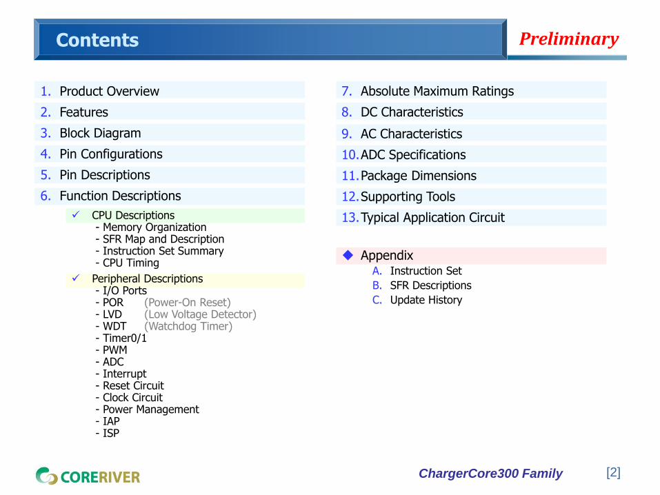
Contents
7. Absolute Maximum Ratings
8. DC Characteristics
9. AC Characteristics
10.ADC Specifications
11.Package Dimensions
12.Supporting Tools
13.Typical Application Circuit
Appendix A. Instruction Set
B. SFR Descriptions
C. Update History
1. Product Overview
2. Features
3. Block Diagram
4. Pin Configurations
5. Pin Descriptions
6. Function Descriptions
CPU Descriptions - Memory Organization - SFR Map and Description - Instruction Set Summary - CPU Timing
Peripheral Descriptions - I/O Ports - POR (Power-On Reset) - LVD (Low Voltage Detector) - WDT (Watchdog Timer) - Timer0/1 - PWM - ADC - Interrupt - Reset Circuit - Clock Circuit - Power Management - IAP - ISP

ChargerCore300 Family
Preliminary
[3]
1. Product Overview
CORERIVER’s Family is a group of fast 80C52 compatible microcontrollers
The instruction execution is max. 3 times faster than that of traditional
80C52.
1 Machine cycle = 4 clocks vs. 12 clocks
Additional peripherals of ChargerCore300 Family:
10 bit ADC / WDT / LVD / POR.
Power saving modes
Noise tolerant scheme
Support ISP / IAP of FLASH memory
Provides Easy-to-Use training-kit system
The Brief Manual contents could be updated at any time. Please check
update contents from CORERIVER Web Site (http://www.coreriver.com)
ChargerCore300 Family
Preliminary
[4]
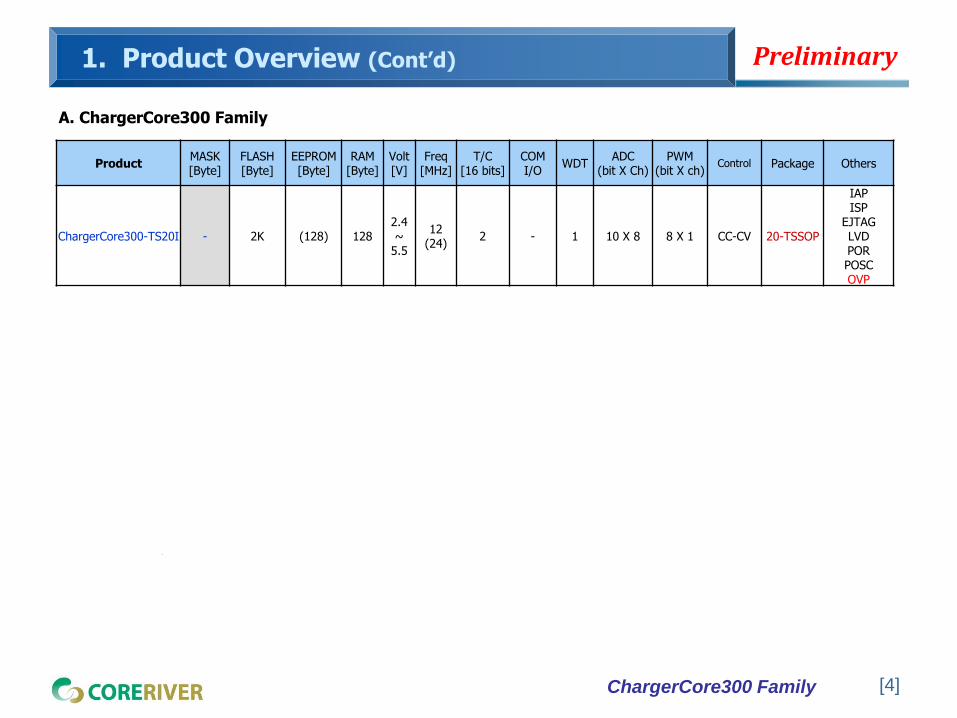
1. Product Overview (Cont’d)
A. ChargerCore300 Family
Product MASK [Byte]
FLASH [Byte]
EEPROM [Byte]
RAM [Byte]
Volt [V]
Freq [MHz]
T/C [16 bits]
COM I/O
WDT ADC
(bit X Ch) PWM
(bit X ch) Control Package Others
ChargerCore300-TS20I - 2K (128) 128 2.4 ~
5.5
12 (24)
2 - 1 10 X 8 8 X 1 CC-CV 20-TSSOP
IAP ISP
EJTAG LVD POR POSC OVP

ChargerCore300 Family
Preliminary
[5]
2. Features
CPU
8-bit turbo 80C52 architecture
4 cycles/1 machine cycle
instruction level compatible with Intel 80C52
2kB FLASH (Including 128B User EEPROM)
Support ISP/IAP of FLASH
128B Internal RAM
Operating Voltage MCU : +2.4V to +5.5V
CC/CV Controller : +2.5V to +12.0V
Operating Frequency (FSYS)
3.68MHz (Internal Clock, Default)
Max. 11.0592MHz (Internal Clock)
Max. 24MHz @4.5V ~ 5.5V (External Clock)
Operating temperature MCU : -40 to 85
CC/CV Controller : 0 to 85
Max. Programmable 12 I/O Pins
Pull-up control, Open drain, & Push-Pull output
TTL and CMOS compatible logic levels
Configurable Low Voltage Detector (LVD)
Internal Precision OSC with Calibration function
3.6864MHz @+2.4 V to +3.3 V ( 1%)
8-channel 10-bit ADC
Max. 120k SPS @FADC = 12MHz
Programmable Input Clock Frequency
1-channel 8-bit High Speed PWM
23-bit Programmable Watchdog Timer (WDT)
Two 16-bit Timer/Counters
Max. 7 Interrupt Sources Timer0/1, WDT, ADC, PWM
2 External Interrupt Sources : Both Edge/Level
Two-level Interrupt Priority
Reset Sources On-chip Power-On-Reset (POR)
External Reset
Configurable Low Voltage Detector Reset (LVR)
Watchdog Timer Reset
Power Down Wake-up Sources Reset Sources + 2 External Interrupt (Low Level)
WDT interrupt
Power Consumption (TBD) Active Current : Max. 2mA @+3.0V, 2MHz
Idle Current : Max. 0.5mA @+3.0V, 2MHz
Stop Current : Max. 1uA @+5.0V (All Clock OFF)
E.S.D. Protection up to 2,000 V
Latch-up Protection Up to 200mA
Package 20-TSSOP
ChargerCore300 Family
Preliminary
[6]
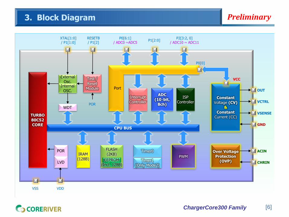
3. Block Diagram
IRAM (128B)
CPU BUS
Interrupt Controller
VDD
Timer0
Timer1 (Only Mode2)
Port
ISP Controller
WDT
XTAL[1:0] / P1[1:0]
TURBO 80C52 CORE
External Osc.
Internal OSC.
PWM
P2[3:2, 0] / ADC10 ~ ADC11
ADC (10-bit,
8ch)
VSS
POR
LVD
RESETB / P1[2]
POR
Test / Reset
Module
FLASH (2KB)
EEPROM (Incl. 128B)
Constant Voltage (CV)
& Constant
Current (CC)
OUT
VCC
GND
VCTRL
VSENSE
P0[6:1] / ADC0 ~ADC5
P1[2:0]
Over Voltage Protection
(OVP)
P0[0]
CHRIN
ACIN

ChargerCore300 Family
Preliminary
[7]
4. Pin Configurations
ADC Channel : 8 Channels
Ordering Information : ChargerCore300-TS20IP
I/O : 12 Pins
[ 20-pin TSSOP : JEDEC]
P0.0 / INT0B / PWM_A / TVO CC-CV VCC
Internal connection
VSS
P1.0 / XTAL1
P1.1 / XTAL2
CC-CV GND
OUT
T0 / P2.0
ADC11 / P2.2
ADC10 / P2.3
1
2
3
4
5
6
7
8
9
10
20
19
18
17
16
15
14
13
12
11
VDD VSENSE
VCTRL
P0.1 / ADC0 / INT1B / ISP_SCL
P0.2 / ADC1 / ISP_SDA
P0.4 / ADC3
P0.5 / ADC4
P0.6 / ADC5 / PWM
P1.2 / RESETB
Charg
erC
ore
300-T
S20IP
P0.3 / ADC2
CHRIN ACIN
ISP / MDS Pin Configuration
RESETB
VSS
ISP_SCL
ISP_SDA
VDD
ChargerCore300 Family
Preliminary
[8] [8]
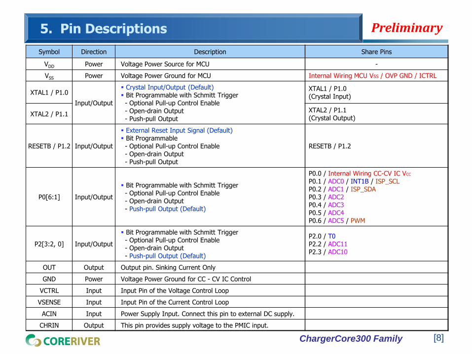
5. Pin Descriptions
Symbol Direction Description Share Pins
VDD Power Voltage Power Source for MCU -
VSS Power Voltage Power Ground for MCU Internal Wiring MCU VSS / OVP GND / ICTRL
XTAL1 / P1.0
Input/Output
Crystal Input/Output (Default) Bit Programmable with Schmitt Trigger - Optional Pull-up Control Enable - Open-drain Output - Push-pull Output
XTAL1 / P1.0 (Crystal Input)
XTAL2 / P1.1 XTAL2 / P1.1 (Crystal Output)
RESETB / P1.2 Input/Output
External Reset Input Signal (Default) Bit Programmable - Optional Pull-up Control Enable - Open-drain Output - Push-pull Output
RESETB / P1.2
P0[6:1] Input/Output
Bit Programmable with Schmitt Trigger - Optional Pull-up Control Enable - Open-drain Output - Push-pull Output (Default)
P0.0 / Internal Wiring CC-CV IC VCC
P0.1 / ADC0 / INT1B / ISP_SCL P0.2 / ADC1 / ISP_SDA P0.3 / ADC2 P0.4 / ADC3
P0.5 / ADC4 P0.6 / ADC5 / PWM
P2[3:2, 0] Input/Output
Bit Programmable with Schmitt Trigger - Optional Pull-up Control Enable - Open-drain Output - Push-pull Output (Default)
P2.0 / T0 P2.2 / ADC11 P2.3 / ADC10
OUT Output Output pin. Sinking Current Only
GND Power Voltage Power Ground for CC - CV IC Control
VCTRL Input Input Pin of the Voltage Control Loop
VSENSE Input Input Pin of the Current Control Loop
ACIN Input Power Supply Input. Connect this pin to external DC supply.
CHRIN Output This pin provides supply voltage to the PMIC input.
ChargerCore300 Family
Preliminary
[9]
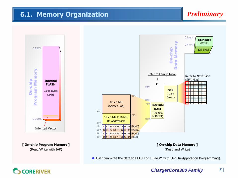
6.1. Memory Organization
07FFh
0000h
Interrupt Vector
On
-ch
ip
Pro
gra
m M
em
ory
Internal FLASH
07FFh
0780h
On
-ch
ip
Data
M
em
ory EEPROM
(MOVX)
[ On-chip Program Memory ]
(Read/Write with IAP)
[ On-chip Data Memory ]
(Read and Write)
SFR (Only
Direct)
Internal
RAM (Indirect
or Direct) 00h
80h
7Fh
FFh
Refer to Family Table
30h
80 x 8 bits
(Scratch Pad)
7Fh
20h
16 x 8 bits (128 bits)
Bit Addressable
2Fh
18h R0 R1 R2 R3 R4 R5 R6 R7 BANK3
10h R0 R1 R2 R3 R4 R5 R6 R7 BANK2
08h R0 R1 R2 R3 R4 R5 R6 R7 BANK1
00h R0 R1 R2 R3 R4 R5 R6 R7 BANK0
Refer to Next Slide. (SFR Map)
2,048 Bytes
(2KB)
128 Bytes
User can write the data to FLASH or EEPROM with IAP (In-Application Programming).
ChargerCore300 Family
Preliminary
[10]
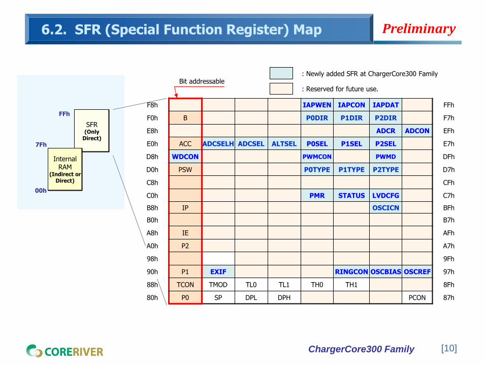
6.2. SFR (Special Function Register) Map
Bit addressable
F8h IAPWEN IAPCON IAPDAT FFh
F0h B P0DIR P1DIR P2DIR F7h
E8h ADCR ADCON EFh
E0h ACC ADCSELH ADCSEL ALTSEL P0SEL P1SEL P2SEL E7h
D8h WDCON PWMCON PWMD DFh
D0h PSW P0TYPE P1TYPE P2TYPE D7h
C8h CFh
C0h PMR STATUS LVDCFG C7h
B8h IP OSCICN BFh
B0h B7h
A8h IE AFh
A0h P2 A7h
98h 9Fh
90h P1 EXIF RINGCON OSCBIAS OSCREF 97h
88h TCON TMOD TL0 TL1 TH0 TH1 8Fh
80h P0 SP DPL DPH PCON 87h
: Newly added SFR at ChargerCore300 Family
: Reserved for future use.
SFR (Only
Direct)
FFh
Internal RAM
(Indirect or Direct)
00h
7Fh

ChargerCore300 Family
Preliminary
[11]
6.2. SFR Brief Description
80C52 SFR Registers
Register Name Reset Value
ACC B PSW SP
Accumulator B Program Status Word Stack Pointer
00000000 00000000 00000000 00000111
DPTR DPL DPH
Data Pointer (2 bytes) Low Byte High Byte
00000000 00000000
P0 P1 P2
Port 0 Port 1 Port 2
11111111 *****111 *1111111
IP IE
Interrupt Priority Interrupt Enable Control
10000000 00000000
TCON TMOD
Timer/Counter 0/1 Control Timer/Counter 0 Mode Control
00000000 ****0000
TH0 TL0 TH1 TL1
Timer/Counter 0 High Byte Timer/Counter 0 Low Byte Timer/Counter 1 High Byte Timer/Counter 1 Low Byte
00000000 00000000 00000000 00000000
PCON Power Control ***10000
Register Name Reset Value
P0SEL P1SEL P2SEL
Port 0 Pull-up Control Port 1 Pull-up Control Port 2 Pull-up Control
11111100 *****011 *1111111
P0TYPE P1TYPE P2TYPE
Port 0 Type Control Port 1 Type Control Port 2 Type Control
00000000 *****000 *0000000
P0DIR P1DIR P2DIR
Port 0 Input/Output Control Port 1 Input/Output Control Port 2 Input/Output Control
11111111 *****111 *1111111
ALTSEL Alternative Function Control 00000***
ADCON ADCR ADCSEL ADCSELH
ADC Control & ADC Result Low ADC Result High ADC Channel Selection Low and MUX Selection ADC High Channel Selection
00100000 00000000 11111111 11111111
EXIF WDCON PMR STATUS LVDCFG
Added External Interrupt and POR Control Watchdog Timer Control Power Management Control Crystal Status LVD Configuration
****0111 110*0000 ****0*** ***0**** 00000101
OSCICN RINGCON OSCBIAS OSCREF
Internal Precision Oscillator Control Internal Precision Oscillator Frequency Tuning Internal Precision Oscillator Bias Current Tuning Internal Precision Oscillator Reference Tuning
****0100 10000000 01011111 ***10111
IAPWEN IAPCON IAPDAT
IAP Write Enable IAP Control IAP Data
00000000 00000000 00000000
* : Don’t touch bit. Read as ‘0’.
Newly added SFR Registers at ChargerCore300 Family
ChargerCore300 Family
Preliminary
[12]
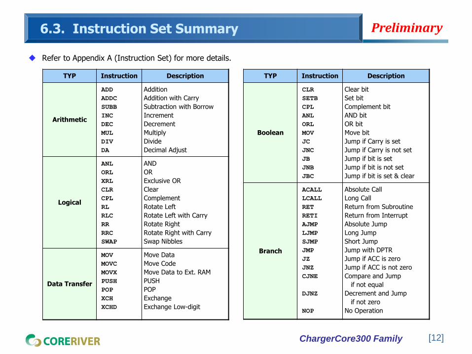
6.3. Instruction Set Summary
Refer to Appendix A (Instruction Set) for more details.
TYP Instruction Description
Arithmetic
ADD
ADDC
SUBB
INC
DEC
MUL
DIV
DA
Addition
Addition with Carry
Subtraction with Borrow
Increment
Decrement
Multiply
Divide
Decimal Adjust
Logical
ANL
ORL
XRL
CLR
CPL
RL
RLC
RR
RRC
SWAP
AND
OR
Exclusive OR
Clear
Complement
Rotate Left
Rotate Left with Carry
Rotate Right
Rotate Right with Carry
Swap Nibbles
Data Transfer
MOV
MOVC
MOVX
PUSH
POP
XCH
XCHD
Move Data
Move Code
Move Data to Ext. RAM
PUSH
POP
Exchange
Exchange Low-digit
TYP Instruction Description
Boolean
CLR
SETB
CPL
ANL
ORL
MOV
JC
JNC
JB
JNB
JBC
Clear bit
Set bit
Complement bit
AND bit
OR bit
Move bit
Jump if Carry is set
Jump if Carry is not set
Jump if bit is set
Jump if bit is not set
Jump if bit is set & clear
Branch
ACALL
LCALL
RET
RETI
AJMP
LJMP
SJMP
JMP
JZ
JNZ
CJNE
DJNZ
NOP
Absolute Call
Long Call
Return from Subroutine
Return from Interrupt
Absolute Jump
Long Jump
Short Jump
Jump with DPTR
Jump if ACC is zero
Jump if ACC is not zero
Compare and Jump
if not equal
Decrement and Jump
if not zero
No Operation
ChargerCore300 Family
Preliminary
[13]
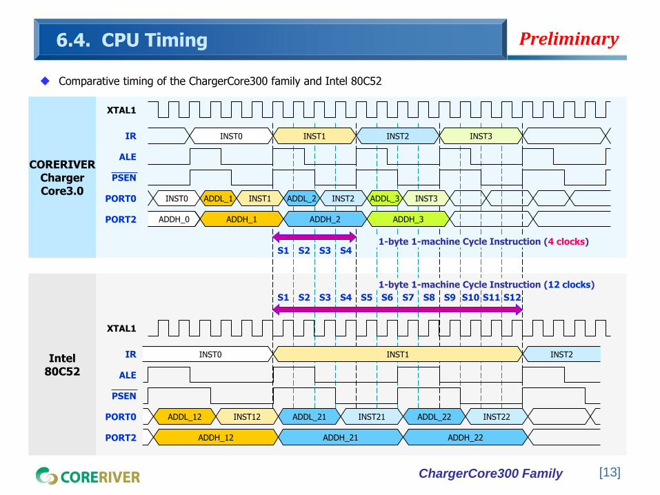
Intel 80C52
CORERIVER Charger Core3.0
6.4. CPU Timing
ADDH_0 ADDH_1 ADDH_2 ADDH_3
INST0 ADDL_1 INST1 ADDL_2 INST2 ADDL_3 INST3
INST0 INST2 INST3 INST1
XTAL1
IR
ALE
PORT0
PORT2
S1 S2 S3 S4 1-byte 1-machine Cycle Instruction (4 clocks)
Comparative timing of the ChargerCore300 family and Intel 80C52
ADDH_21
ADDL_21 INST21
ADDH_22
ADDL_22 INST22
ADDH_12
ADDL_12 INST12
INST0 INST1
XTAL1
IR
ALE
PORT0
PORT2
INST2
1-byte 1-machine Cycle Instruction (12 clocks)
S1 S2 S3 S4 S5 S6 S7 S8 S9 S10 S11 S12
PSEN
PSEN

ChargerCore300 Family
Preliminary
[14]
6.4. CPU Timing : Execution Time Table
The fastest instruction execution in the world
Instruction ChargerCore300
(CORERIVER) W77C32
(Winbond) DS80C320 (Maxim)
87C52 (Intel)
MUL AB
DIV AB 12 clocks 20 clocks 20 clocks 48 clocks
MOVC A, @A+PC
MOVC A, @A+DPTR 8 clocks 8 clocks 12 clocks 24 clocks
JMP @A+DPTR 8 clocks 8 clocks 12 clocks 24 clocks
RET
RETI 8 clocks 8 clocks 16 clocks 24 clocks
INC DPTR 4 clocks 8 clocks 12 clocks 24 clocks
Others Same Same Same -

ChargerCore300 Family
Preliminary
[15]
6.5. I/O Ports : PORT0[6:0]
Open-drain or push-pull Output.
The alternative functions are available only when the corresponding SFR bit is “1”.
P0.0 = INT0B, PWM_A, TVO / PWM0.1 = ADC0, INT1B, ISP_SCL / P0.2 = ADC1, ISP_SDA / P0.4 = ADC3 / P0.5 = ADC4 / P0.6 = ADC5, PWM
Read-Modify-Write instructions do not read port pin but SFR register.
ANL / ORL / XRL / JBC / CPL / INC / DEC / DJNZ / MOV PX.Y, C / CLR PX.Y / SETB PX.Y
- P0SEL.6 P0SEL.5 P0SEL.4 P0SEL.3 P0SEL.2 P0SEL.1 P0SEL.0
R/W(1) R/W(1) R/W(1) R/W(1) R/W(1) R/W(1) R/W(0) R/W(0)
P0SEL (E4h) : Port 0 Pull-up Control Register
0 = Pull-up resistor ON / 1 = Pull-up resistor OFF
- P0.6 P0.5 P0.4 P0.3 P0.2 P0.1 P0.0
R/W(1) R/W(1) R/W(1) R/W(1) R/W(1) R/W(1) R/W(1) R/W(1)
P0 (80h) : Port 0 Register
- P0TYPE.6 P0TYPE.5 P0TYPE.4 P0TYPE.3 P0TYPE.2 P0TYPE.1 P0TYPE.0
R/W(0) R/W(0) R/W(0) R/W(0) R/W(0) R/W(0) R/W(0) R/W(0)
P0TYPE (D4h) : Port 0 Type Control Register
0 = Push-pull Output (Default) / 1 = Open-drain Output
- P0DIR.6 P0DIR.5 P0DIR.4 P0DIR.3 P0DIR.2 P0DIR.1 P0DIR.0
R/W(1) R/W(1) R/W(1) R/W(1) R/W(1) R/W(1) R/W(1) R/W(1)
P0DIR (F4h) : Port 0 Input/Output Control Register
0 = Output / 1 = Input (Default)
ADC3B ADC2B ADC1B ADC0B CH3 CH2 CH1 CH0
R/W(1) R/W(1) R/W(1) R/W(1) R/W(1) R/W(1) R/W(1) R/W(1)
ADCSEL (E2h) : ADC Channel Selection Low & MUX Selection
ADCXB = 0 : ADCX Input Enable & Digital Input Disable
P0.1 P0.1 SFR
Q
QB
CPU BUS
Pull- up
P0SEL.1 P0TYPE.1 P0DIR.1
0
1 Alternative Output
Alternative Enable
ADC0 Input
ADC0B
Digital Input

ChargerCore300 Family
Preliminary
[16]
6.5. I/O Ports : PORT1[1:0] (XTAL1/XTAL2)
XTAL1/XTAL2 can be configured as I/O port.
Read-Modify-Write instructions do not read port pin but SFR register.
ANL / ORL / XRL / JBC / CPL / INC / DEC / DJNZ / MOV PX.Y, C / CLR PX.Y / SETB PX.Y
- - - - - P1TYPE.2 P1TYPE.1 P1TYPE.0
R/W(0) R/W(0) R/W(0)
P1TYPE (D5h) : Port 1 TYPE Control Register
0 = Push-pull Output (Default) / 1 = Open-drain Output
- - - - - P1.2 P1.1 P1.0
R/W(1) R/W(1) R/W(1)
P1 (90h) : Port 1 Register
- - - - XTOFF - - -
R/W(0)
PMR (C4h) : Power Management Control Register
- - - - - P1DIR.2 P1DIR.1 P1DIR.0
R/W(1) R/W(1) R/W(1)
P1DIR (F5h) : Port 1 Input/Output Control Register
0 = Output / 1 = Input (Default)
- - - - - P1SEL.2 P1SEL.1 P1SEL.0
R/W(0) R/W(1) R/W(1)
P1SEL (E5h) : Port 1 Pull-up Control Register
0 = Pull-up resistor ON / 1 = Pull-up resistor OFF
XTAL_IOEN RST_IOEN CLO PWM00 TV0 - - -
R/W(0) R/W(0) R/W(0) R/W(0) R/W(0)
ALTSEL (85h) : Alternative Function Control Register
XTAL_IOEN = 1 : XTAL1 and XTAL2 are configured as I/O Ports
Digital Input
Pull- up
XTAL1 / P1.0
Digital Input
Pull- up
XTAL2 / P1.1
P1.0 SFR
Q
QB
CPU BUS
P1.1 SFR
Q
QB
CPU BUS
P1SEL.1 P1TYPE.1 P1DIR.1
P1SEL.0 P1TYPE.0 P1DIR.0 XTAL_IOEN
AMP
XTOFF
ChargerCore300 Family
Preliminary
[17]
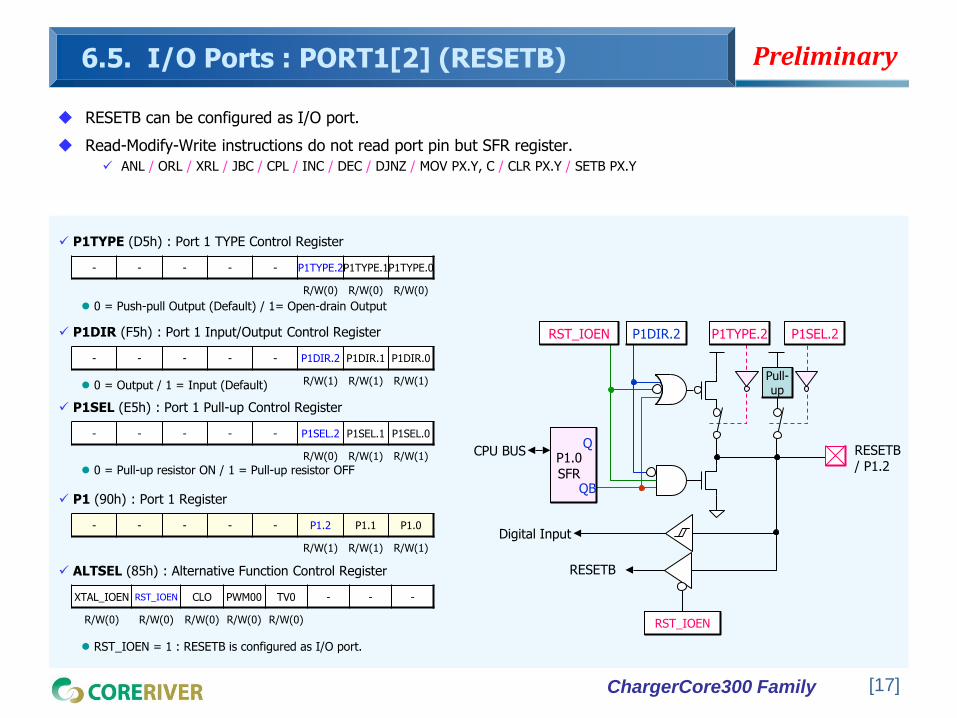
6.5. I/O Ports : PORT1[2] (RESETB)
RESETB can be configured as I/O port.
Read-Modify-Write instructions do not read port pin but SFR register.
ANL / ORL / XRL / JBC / CPL / INC / DEC / DJNZ / MOV PX.Y, C / CLR PX.Y / SETB PX.Y
XTAL_IOEN RST_IOEN CLO PWM00 TV0 - - -
R/W(0) R/W(0) R/W(0) R/W(0) R/W(0)
ALTSEL (85h) : Alternative Function Control Register
RST_IOEN = 1 : RESETB is configured as I/O port.
- - - - - P1TYPE.2 P1TYPE.1 P1TYPE.0
R/W(0) R/W(0) R/W(0)
P1TYPE (D5h) : Port 1 TYPE Control Register
0 = Push-pull Output (Default) / 1= Open-drain Output
- - - - - P1.2 P1.1 P1.0
R/W(1) R/W(1) R/W(1)
P1 (90h) : Port 1 Register
- - - - - P1DIR.2 P1DIR.1 P1DIR.0
R/W(1) R/W(1) R/W(1)
P1DIR (F5h) : Port 1 Input/Output Control Register
0 = Output / 1 = Input (Default)
- - - - - P1SEL.2 P1SEL.1 P1SEL.0
R/W(0) R/W(1) R/W(1)
P1SEL (E5h) : Port 1 Pull-up Control Register
0 = Pull-up resistor ON / 1 = Pull-up resistor OFF
Digital Input
Pull- up
RESETB / P1.2
P1.0 SFR
Q
QB
CPU BUS
P1SEL.2 P1TYPE.2 P1DIR.2 RST_IOEN
RESETB
RST_IOEN

ChargerCore300 Family
Preliminary
[18]
6.5. I/O Ports : PORT2[3:2]
Open-drain or push-pull output.
The alternative functions are available only when the corresponding SFR bit is “1”.
P2.2 = ADC11 / P2.3 = ADC10 / P2.4 = ADC9
Read-Modify-Write instructions do not read port pin but SFR register.
ANL / ORL / XRL / JBC / CPL / INC / DEC / DJNZ / MOV PX.Y, C / CLR PX.Y / SETB PX.Y
- - - - P2TYPE.3 P2TYPE.2 - -
R/W(0)) R/W(0) R/W(0) R/W(0) R/W(0) R/W(0) R/W(0)
P2TYPE (D6h) : Port 2 Type Control Register
0 = Push-pull Output (Default) / 1= Open-drain Output
- - - - P2.3 P2.2 - -
R/W(1) R/W(1) R/W(1) R/W(1) R/W(1) R/W(1) R/W(1)
P2 (A0h) : Port 2 Register
- - - - P2DIR.3 P2DIR.2 - -
R/W(1) R/W(1) R/W(1) R/W(1) R/W(1) R/W(1) R/W(1)
P2DIR (F6h) : Port 2 Input/Output Control Register
0 = Output / 1 = Input (Default)
ADC11 Input
ADC11B
P2.2
Digital Input
P2.2 SFR
Q
QB
CPU BUS
Pull- up
P2SEL.2 P2TYPE.2 P2DIR.2
0
1 Alternative Output
Alternative Enable - - - - P2SEL.3 P2SEL.2 - -
R/W(1) R/W(1) R/W(1) R/W(1) R/W(1) R/W(1) R/W(1)
P2SEL (E6h) : Port 2 Pull-up Control Register
0 = Pull-up resistor ON / 1 = Pull-up resistor OFF (Default)
ADC11B ADC10B - - - - ADC5B ADC4B
R/W(1) R/W(1) R/W(1) R/W(1) R/W(1) R/W(1) R/W(1) R/W(1)
ADCSELH (E1h) : ADC Channel Selection High Register
ADCXB = 0 : ADCX Input Enable & Digital Input Disable

ChargerCore300 Family
Preliminary
[19]
6.5. The ESD Structure of Pads
Two ESD diodes and one ESD resister are contained in all pads except VDD.
One ESD diode are contained in VDD.
[VDD]
• Two ESD Diodes (VDD side, VSS side) • One ESD Resister
• One ESD Diode (GND side) • One ESD Resister
[All pads except VDD]

ChargerCore300 Family
Preliminary
[20]
6.6. POR (Power-On Reset)
POR_OFF
POR Pulse POR Reset
PCON.4
POF
POR
5.0
VD
D [
V]
1.6
0
A D
POR Pulse
TIME 1.6V 1.6V
On-chip power-on reset Generate reset when VDD is below 1.6V.
POR block is off during power-down mode if BGS is cleared.
General Flags in PCON[3:2] Cleared only by POR.
Not cleared by other resets.
Maybe used to distinguish cold start reset or warm start reset.
- XT/RG RGMD RGSL BGS
- R/W(0) R(1) R(1) R/W(1)
EXIF (91h) : External Interrupt Flag Register
BGS : Band-gap select (Default = 1).
If 0, Band-gap block (POR) will be off in power-down mode If 1, Band-gap block (POR) will run in power-down mode
- - - POF GF1 GF0 PD IDL
R/W(1) R/W(0) R/W(0) R/W(0) R/W(0)
PCON (87h) : Power Control Register
POF : Power off flag. When power-on, this flag bit will be set by H/W. PD : Power-down (Stop) mode enable.
EXIF.0 PCON.1
PD BGS
PFI Pulse
2.4V 2.4V
2.4 B C

ChargerCore300 Family
Preliminary
[21]
6.7. LVD (Configurable Low Voltage Detector)
LVD (Low Voltage Detector)
Provides on-chip power-fail interrupt or reset
PFI pulse is sampled at the end of an instruction (machine cycle if in IDLE mode).
LVD Reset or interrupt is generated if enabled and two continuous samples of PFI pulse are high.
User S/W may generate reset by setting PFI bit two times continuously when EFPR bit is set.
Factory Calibration of LVD
Factory tuning value should be updated by user S/W.
The calibration value is for 2.4V.
User may select the LVD voltage from 2.1V to 2.7V by adding or subtracting numbers to the calibration value.
The LVD voltage is increased by 0.1V if CFG[4:0] is increased by 1.
Since the resolution of calibration is 0.1V, the maximum error of LVD calibration is ± 0.05V.
EPFR EPFI PFI CFG4 CFG3 CFG2 CFG1 CFG0
R/W(0) R/W(0) R/W(0) R/W(0) R/W(0) R(1) R/W(0) R/W(1)
LVDCFG (C6h) : LVD Configuration Register
EPFR : Power-fail reset enable.
EPFI : Power-fail interrupt enable.
PFI : Power-fail interrupt flag.
CFG[4:0] : LVD Voltage Configuration
NOTE : This SFR is initialized only by power-on-reset. That is, it holds user’s setting for any other reset.
LVD Enable
PFI Pulse
PFI interrupt
EPFI
PFI
LVDCFG.6
LVDCFG.5
LVD_H25
PCON.1
PD
EPFR
PFI Reset
EPFR
LVDCFG.7
EPFI
// Read the calibration data for LVD
// and enable interrupt for 2.1V
void init_lvd_intr(void)
DPH = 0;
DPL = 8; // Data address
IAPCON = 0x0D; // Read byte in OTP
LVDCFG = IAPDAT; // Configuration for 2.4V
LVDCFG -= 3; // Configuration for 2.1V
LVDCFG |= 0x40; // Enable LVD Interrupt

ChargerCore300 Family
Preliminary
[22]
6.8. WDT (Watch Dog Timer)
Detects software upset due to external noise or other causes
Allows an automatic recovery using WDT interrupt
If enabled, WDT interrupt or WDT reset makes MCU wake up from stop mode.
Watchdog time-out values
WD1 WD0 WDM - WDIF WTRF EWT RWT
R/W(1) R/W(1) R/W(0) R(0) R/W(0) R/W(0) R/W(0) R/W(0)
WDCON (D8h) : Watchdog Timer & Power Status Register
WD[1:0] : WDT Clock Divide WDM : Watchdog clock divide mode for Test (Do not set this bit in the application.) WDIF : Watchdog Timer Interrupt Flag WTRF : Watchdog Timer Reset Flag EWT : Watchdog Timer Reset Enable RWT : Restart Watchdog Timer
WD1 WD0 Interrupt Time-out (@ 4MHz) Reset Time-out
0 0 219 clocks 131 ms 219 + 512 clocks
0 1 220 clocks 262 ms 220 + 512 clocks
1 0 221 clocks 524 ms 221 + 512 clocks
1 1 222 clocks 1048 ms 222 + 512 clocks
WD1 WD0
11
WDCON[7:6]
10
01
00
EWDT
512 clocks Delay
IE.4
Interrupt
EWT WDCON.1
WTRF WDCON.2
WDT Reset
WDIF
WDCON.3 23-bit Counter
CLK
RWT
RESET
WDCON.0
22 21 20 19 18 1 0

ChargerCore300 Family
Preliminary
[23]
6.9. Timer/Counter : Timer 0/1
Compatible with traditional 80C52 Timer/Counter function
Time base is 12 clocks.
Mode
Timer
Mode 0
(M1,M0=00)
Mode 1
(M1,M0=01)
Mode 2
(M1,M0=10)
Mode 3
(M1,M0=11)
Timer0 13-bit T/C 16-bit T/C
8-bit T/C with automatic reload
(TL0 TH0)
8-bit T/C (TL0)
Timer0 interrupt
8-bit T/C (TH0)
Timer1 interrupt
Timer1 Not Supported
8-bit T/C with automatic reload
(TL1 TH1)
Not Supported
- - - - GATE C/T M1 M0
R/W(0) R/W(0) R/W(0) R/W(0)
TMOD (89h) : Timer/Counter 0 Mode Control Register
GATE : Timer 0 Gate control. When TRx (in TCON) is set and GATE=1, Timer x will run only while INTx pin is high (hardware control). When GATE=0, Timer x will run only while TRx=1 (software control). C/T[2] : Timer 0 Counter/Timer Select. 0 = Timer by FOSC/12. (Default) 1 = Counter by T0 pin. M1, M0 : Timer 0 Mode Select. [0,0] : Mode 0. 13-bit T/C. [0,1] : Mode 1. 16-bit T/C. [1,0] : Mode 2. 8-bit T/C with automatic reload [1,1] : Mode 3. Two 8-bit T/C
TF1 TR1 TF0 TR0 IE1 IT1 IE0 IT0
R/W(0) R/W(0) R/W(0) R/W(0) R/W(0) R/W(0) R/W(0) R/W(0)
TCON (88h) : Timer/Counter 0/1 Control Register
TF1 : Timer 1 Overflow Flag. TR1 : Timer 1 Run Enable. TF0 : Timer 0 Overflow Flag. TR0 : Timer 0 Run Enable. IE1 : External Interrupt 1 Flag. IT1 : External Interrupt 1 TYP Select Flag. Falling Edge Detect (IT1=1). Low Level Detect (IT1=0). IE0 : External Interrupt 0 Flag. IT0 : External Interrupt 0 TYP Select Flag. Falling Edge Detect (IT0=1). Low Level Detect (IT0=0).
TL0.7 TL0.6 TL0.5 TL0.4 TL0.3 TL0.2 TL0.1 TL0.0
R/W(0) R/W(0) R/W(0) R/W(0) R/W(0) R/W(0) R/W(0) R/W(0)
TL0 (8Ah) : Timer/Counter 0 Low Byte Register
TH0.7 TH0.6 TH0.5 TH0.4 TH0.3 TH0.2 TH0.1 TH0.0
R/W(0) R/W(0) R/W(0) R/W(0) R/W(0) R/W(0) R/W(0) R/W(0)
TH0 (8Ch) : Timer/Counter 0 High Byte Register
TL1.7 TL1.6 TL1.5 TL1.4 TL1.3 TL1.2 TL1.1 TL1.0
R/W(0) R/W(0) R/W(0) R/W(0) R/W(0) R/W(0) R/W(0) R/W(0)
TL1 (8Bh) : Timer/Counter 1 Low Byte Register
TH1.7 TH1.6 TH1.5 TH1.4 TH1.3 TH1.2 TH1.1 TH1.0
R/W(0) R/W(0) R/W(0) R/W(0) R/W(0) R/W(0) R/W(0) R/W(0)
TH1 (8Dh) : Timer/Counter 1 High Byte Register

ChargerCore300 Family
Preliminary
[24]
[Mode 1]
FOSC 1/12
T0 PIN
TF0 Interrupt
CONTROL
TL0 (8bits)
TH0 (8bits)
GATE
INT0B PIN
TR0
1
0
C/T
TMOD.2
When C/T = 0 (Default),
[Mode 3]
6.9. Timer/Counter : Timer 0 Mode Description
[Mode 2]
FOSC 1/12
T0 PIN
TF0 Interrupt
CONTROL
TL0 (8bits)
TH0 (8bits)
RELOAD
GATE
INT0B PIN
TR0
FOSC 1/12
T0 PIN
Timer 0 Interrupt
CONTROL
GATE
INT0B PIN
TL0 (8bits)
TF0
TH0 (8bits)
TF1 Timer 1 Interrupt
CONTROL
FOSC 1/12
TR0
TR1
[Mode 0]
FOSC 1/12
T0 PIN
TF0 Interrupt
CONTROL
TL0 (5bits)
TH0 (8bits)
GATE
INT0B PIN
TR0
1
0
C/T
TMOD.2
1
0
C/T
TMOD.2
1
0
C/T
TMOD.2
13
1
OSC 212
FTime[sec]
16
1
OSC 212
FTime[sec]
TH0212
FTime[sec] 8
1
OSC
When C/T = 0 (Default),
When C/T = 0 (Default),

ChargerCore300 Family
Preliminary
[25]
6.9. Timer/Counter : Timer 1 Mode Description
[Mode 2]
TF1 Interrupt
CONTROL
TL1 (8bits)
TH1 (8bits)
RELOAD
FOSC 1/12
TR1
ChargerCore300 Family
Preliminary
[26]
6.10. PWM (Pulse Width Modulator)
Intelligent 1-channel 8-bit PWM
PWM Counter Reload Mode (8-bit Counter Overflow Reload)
PWM Counter can be cleared by S/W.
PWM is stopped or started (resumed) by S/W.
FOSC
8-bit Buffer
PWMD
8-bit
PWM Pulse
Generation
PWM Counter
0 1 2 3 4 5 6 7
Clear
Overflow
Set
PWMCON[6:4]
Comparator
Clock Divide (1/2/4/8/16/32/64/128)
PWM06 PS2_P0 PS1_P0 PS0_P0 - PWMF CLR_P0 RUN_P0
R/W(0) R/W(0) R/W(0) R/W(0) R/W(0) R/W(0) R/W(0)
PWMCON (DCh) : PWM Control Register
PWM06 : PWM Waveform Output Enable to P0.6
PS2_P0, PS1_P0, PS0_P0 : Pre-scaled Clock Selection.
[0,0,0] = FOSC/1, [0,0,1] = FOSC/2, [0,1,0] = FOSC/4,
[0,1,1] = FOSC/8, [1,0,0] = FOSC/16, [1,0,1] = FOSC/32,
[1,1,0] = FOSC/64, [1,1,1] = FOSC/128
PWMF : PWM Interrupt Flag. Cleared by S/W
CLR_P0 : Counter Reset Enable. Cleared by H/W.
RUN_P0 : Counter Start Enable.
PWMD.7 PWMD.6 PWMD.5 PWMD.4 PWMD.3 PWMD.2 PWMD.1 PWMD.0
R/W(0) R/W(0) R/W(0) R/W(0) R/W(0) R/W(0) R/W(0) R/W(0)
PWMD (DEh) : PWM Duty Data Register
XTAL_IOEN RST_IOEN CLO PWM00 TV0 - - -
R/W(0) R/W(0) R/W(0) R/W(0) R/W(0)
ALTSEL (E3h) : Alternative Function Control Register
PWM00 : PWM Waveform Output Enable to P0.0
P0.6
P0.0
PWM00
PWM06
FPWM

ChargerCore300 Family
Preliminary
[27]
6.10. PWM : Pulse Generation
Clock Count 000h
Clock Count 100h
Clock Count 200h
Clock Count 300h
Clock Count 400h
PWM Clock (FOSC/1)
PWM Out
PWM Out
PWM Out
PWM Out
1 Clock Cycle
Low
(50% Duty)
1 Clock Cycle
(PWMD = 00h)
(PWMD = 01h)
(PWMD = 80h)
(PWMD = FFh)
ChargerCore300 Family
Preliminary
[28]
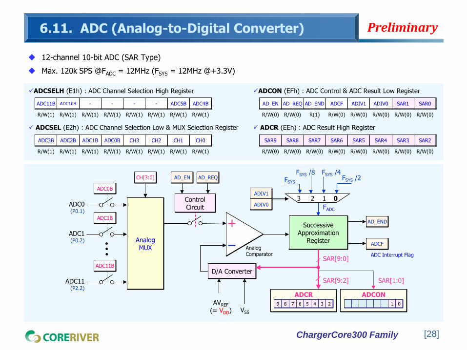
6.11. ADC (Analog-to-Digital Converter)
12-channel 10-bit ADC (SAR Type)
Max. 120k SPS @FADC = 12MHz (FSYS = 12MHz @+3.3V)
Analog MUX
ADC0 (P0.1)
ADC0B
ADC1 (P0.2)
ADC1B
ADC11 (P2.2)
ADC11B
Successive Approximation
Register
FADC
AD_END
ADCF
ADC Interrupt Flag SAR[9:0]
ADCR
9 8 7 6 5 4 3 2
ADCON
1 0
D/A Converter
SAR[9:2] SAR[1:0]
Analog Comparator
VSS
3 2 1 0
FSYS /2 CH[3:0]
Control Circuit
AD_EN AD_REQ
AD_EN AD_REQ AD_END ADCF ADIV1 ADIV0 SAR1 SAR0
R/W(0) R/W(0) R(1) R/W(0) R/W(0) R/W(0) R/W(0) R/W(0)
ADCON (EFh) : ADC Control & ADC Result Low Register
SAR9 SAR8 SAR7 SAR6 SAR5 SAR4 SAR3 SAR2
R/W(0) R/W(0) R/W(0) R/W(0) R/W(0) R/W(0) R/W(0) R/W(0)
ADCR (EEh) : ADC Result High Register
ADC11B ADC10B - - - - ADC5B ADC4B
R/W(1) R/W(1) R/W(1) R/W(1) R/W(1) R/W(1) R/W(1) R/W(1)
ADCSELH (E1h) : ADC Channel Selection High Register
ADC3B ADC2B ADC1B ADC0B CH3 CH2 CH1 CH0
R/W(1) R/W(1) R/W(1) R/W(1) R/W(1) R/W(1) R/W(1) R/W(1)
ADCSEL (E2h) : ADC Channel Selection Low & MUX Selection Register
AVREF
(= VDD)
ADIV1
ADIV0
FSYS /4 FSYS /8 FSYS
ChargerCore300 Family
Preliminary
[29]
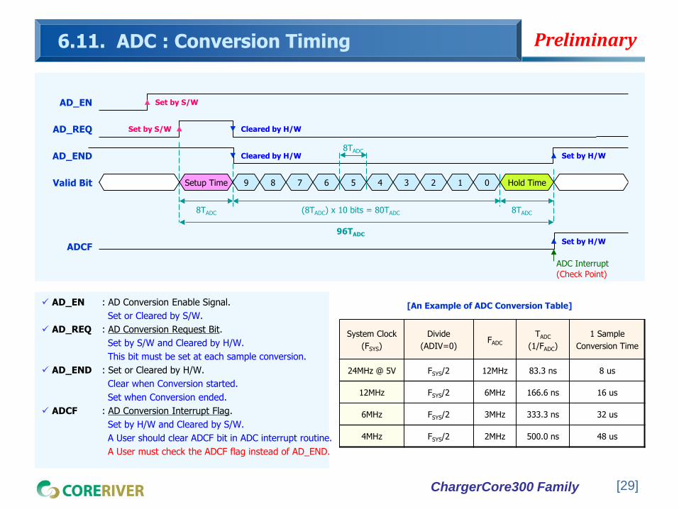
6.11. ADC : Conversion Timing
AD_EN : AD Conversion Enable Signal.
Set or Cleared by S/W.
AD_REQ : AD Conversion Request Bit.
Set by S/W and Cleared by H/W.
This bit must be set at each sample conversion.
AD_END : Set or Cleared by H/W.
Clear when Conversion started.
Set when Conversion ended.
ADCF : AD Conversion Interrupt Flag.
Set by H/W and Cleared by S/W.
A User should clear ADCF bit in ADC interrupt routine.
A User must check the ADCF flag instead of AD_END.
System Clock
(FSYS)
Divide
(ADIV=0) FADC
TADC
(1/FADC)
1 Sample
Conversion Time
24MHz @ 5V FSYS/2 12MHz 83.3 ns 8 us
12MHz FSYS/2 6MHz 166.6 ns 16 us
6MHz FSYS/2 3MHz 333.3 ns 32 us
4MHz FSYS/2 2MHz 500.0 ns 48 us
[An Example of ADC Conversion Table]
9 8 7 6 5 4 Setup Time
AD_EN
AD_REQ
ADCF
AD_END
Valid Bit
Set by S/W
Cleared by H/W
Cleared by H/W
Set by S/W
8TADC (8TADC) x 10 bits = 80TADC
96TADC
8TADC
2 1 0 Hold Time
Set by H/W
Set by H/W
ADC Interrupt
8TADC
3
(Check Point)

ChargerCore300 Family
Preliminary
[30]
6.12. Interrupt : 7 Sources / 2-level Priority
7 Interrupt Sources
Timer 0/1, ADC, WDT, PWM, 2 External.
3-level Interrupt Priority TF1 TR1 TF0 TR0 IE1 IT1 IE0 IT0 TCON (88h)
Interrupt Sources
Address Priority Level
LVD 0033h NMI
INT0B 0003h 2 Levels
TF0 000Bh 2 Levels
INT1B 0013h 2 Levels
TF1 001Bh 2 Levels
WDT 0023h 2 Levels
PWM 002Bh 2 Levels
ADC 003Bh 2 Levels
EA EADC EPWM EWDT ET1 EX1 ET0 EX0 IE (A8h)
- PADC PPWM PWDT PT1 PX1 PT0 PX0 IP (B8h)
WD1 WD0 WDM - WDIF WTRF EWT RWT WDCON (D8h)
* Interrupt related to SFR (refer to Appendix B : SFR Description)
[Interrupt Vector Address]
Interrupt Flag bits
IE0
Individual Enable
bits
EX0
[Interrupt Vector Generation Flow]
Global Enable
bits
EA
Priority bits
Polling & Vector
Generation
0003h PX0
Interrupt Vector
Interrupt Sources
0003h
[Response Sequence]
Sample & Flag Set Polling LCALL Service Routine
Last Cycle & High Priority & Not-update Interrupt Register
PR
IOR
ITY
HIGH
LOW
PWM06 PS2_P0 PS1_P0 PS0_P0 - PWMF CLR_P0 RUN_P0 PWMCON (DCh)
AD_EN AD_REQ AD_END ADCF ADIV1 ADIV0 SAR1 SAR0 ADCON (EFh)
EPFR EPFI PFI CFG4 CFG3 CFG2 CFG1 CFG0 LVDCFG (C6h)

ChargerCore300 Family
Preliminary
High Priority
[31]
6.12. Interrupt Functional Description
High Priority High Priority
Interrupt Vector
Inte
rrup
t Po
lling
Se
qu
en
ce
EX0
ET0
EX1
ET1
EADC
EWDT
Interrupt Enable Bits
INT0B
Timer/Counter 0
INT1B
Timer/Counter 1
ADC
WDT
Flag Bits
1 0 PWDT
PX0
PT0
PX1
PT1
PADC
Priority
IE1
IE0 IT0
IT1
0
0
1
1
Low Priority
1 0
1 0
1 0
1 0
1 0
PWM
1 0 PPWM
TF1
TF0
ADCF
WDIF
PWMF EPWM
EA
LVD (Power Fail) PFI EPFI
Highest
Lowest
Interrupt Level
INT0B & INT1B : Falling Edge Detect (ITX=1), Low Level Detect (ITX=0). The Edge Detection is possible only if the peripheral clock is alive.

ChargerCore300 Family
Preliminary
[32]
6.13. Reset Circuit : Four Reset Sources
Reset Sources
POR reset : Power-on Reset (POR) / Power-fail Reset
LVD reset : Configurable Reset Voltage
External Reset : RESETB must be low for 20 us or more.
WDT reset : Optional control by S/W.
Device Reset Timer
Once set, internal reset remains high until the DRT
(Device Reset Timer) is expired.
The reset time is about 16 ms.
WD1 WD0 WDM - WDIF WTRF EWT RWT
R/W(1) R/W(1) R/W(0) R/W(0) R/W(0) R/W(0)
WDCON (D8h) : Watchdog Timer Control Register
WTRF : Watchdog Timer Reset Flag. Only cleared by S/W. EWT : Watchdog Timer Reset Enable.
Initialize
WDT Counter
VDD
Delay 512 Clocks
WDT RESET Generation
WTRF
EWT
External RESET Generation (Min. 20 us)
LVD RESET Generation
LVD
RESETB
Clock
PFI
Internal RESET
Device Reset Timer (216) FSYS
DRT Reset
Time Out
S
R
Q
VDD POR RESET Generation
POR/LVR
POR
POF

ChargerCore300 Family
Preliminary
[33]
6.14. Clock Circuit
Two System Clock Sources
Internal Precision Oscillator
External Crystal Oscillator
Default System Clock is internal Precision OSC.
User need to check XTUP flag before set XT/RG bit.
Fast Wake-up from Power-down Mode using internal OSC.
- - XT/RG RGMD RGSL BGS
R/W(0) R(1) R(1) R/W(1)
EXIF (91h) : External Interrupt Flag Register
- - - - DIV2 RINGON DIV1 DIV0
R/W(0) R/W(1) R/W(0) R/W(0)
OSCICN (BEh) : Internal Oscillator Control Register
- - - XTUP - - - -
R(0)
STATUS (C5h) : Crystal Status Register
- - - - XTOFF - - -
R/W(0)
PMR (C4h) : Power Management Control Register
- - - POF GF1 GF0 PD IDL
R/W(1) R/W(0) R/W(0) R/W(0) R/W(0)
PCON (87h) : Power Control Register
Control Flag
System Clock
Status Bit
RGMD XTUP XT/RG XTOFF RINGON
1 0 X Crystal OSC. 0 1
0 X 1 Precision OSC. 1 0/1
RGMD DIV[2:0]
XTUP
PD RINGON
PD XTOFF
Clock Switch Control
Clock Stable Circuit
(16 ms)
Divider
XCLK
RCLK
Crystal OSC.
Precision OSC.
12MHz
PD IDL
CPU Clock
Peri. Clock
(System Clock)
XT/RG
FSYS
FOSC

ChargerCore300 Family
Preliminary
[34]
6.14. Clock Circuit
Internal Precision Oscillator with Calibration Function
The default internal clock (RCLK) is 4MHz.
The calibration values are saved in OTP area and should be copied to the tuning registers by user S/W (Refer to IAP example).
- - - - DIV2 RINGON DIV1 DIV0
R/W(0) R/W(1) R/W(0) R/W(0)
OSCICN (BEh) : Internal Oscillator Control Register
RINGON : 1 = Internal oscillator(11.06MHz) is running. 0 = Internal oscillator is off. Don’t clear RINGON bit when XTRG = 0.
DIV2, DIV1, DIV0 : Internal oscillator divider (FPOSC = 11.06MHz) [0,0,0] = 3.68MHz ; Default [0,0,1] = 1.84MHz [0,1,0] = 922KHz [0,1,1] = 461KHz [1,0,0] = reserved [1,0,1] = 11.06MHz [1,1,0] = 5.53MHz [1,1,1] = 2.76MHz
S7 S6 S5 S4 S3 S2 S1 S0
R/W(1) R/W(0) R/W(0) R/W(0) R/W(0) R/W(0) R/W(0) R/W(0)
RINGCON(95h) : Internal Oscillator Frequency Tuning
S7 S6 S5 S4 S3 S2 S1 S0
R/W(0) R/W(1) R/W(0) R/W(1) R/W(1) R/W(1) R/W(1) R/W(1)
OSCBIAS(96h) : Internal Oscillator Bias Current Tuning
- - - S4 S3 S2 S1 S0
R/W(1) R/W(0) R/W(1) R/W(1) R/W(1)
OSCREF(97h) : Internal Oscillator Reference Tuning

ChargerCore300 Family
Preliminary
[35]
6.14. Clock Circuit : Guideline for Configuration
Oscillator Module
OSC
Oscillator Module
Crystal Oscillator Internal Ring Oscillator
Charger Core300 XTAL2
XTAL1
Charger Core300 XTAL2
XTAL1
Charger Core300 XTAL2
XTAL1 RING OSC
RC Oscillator
ChargerCore300 Family
Preliminary
[36]
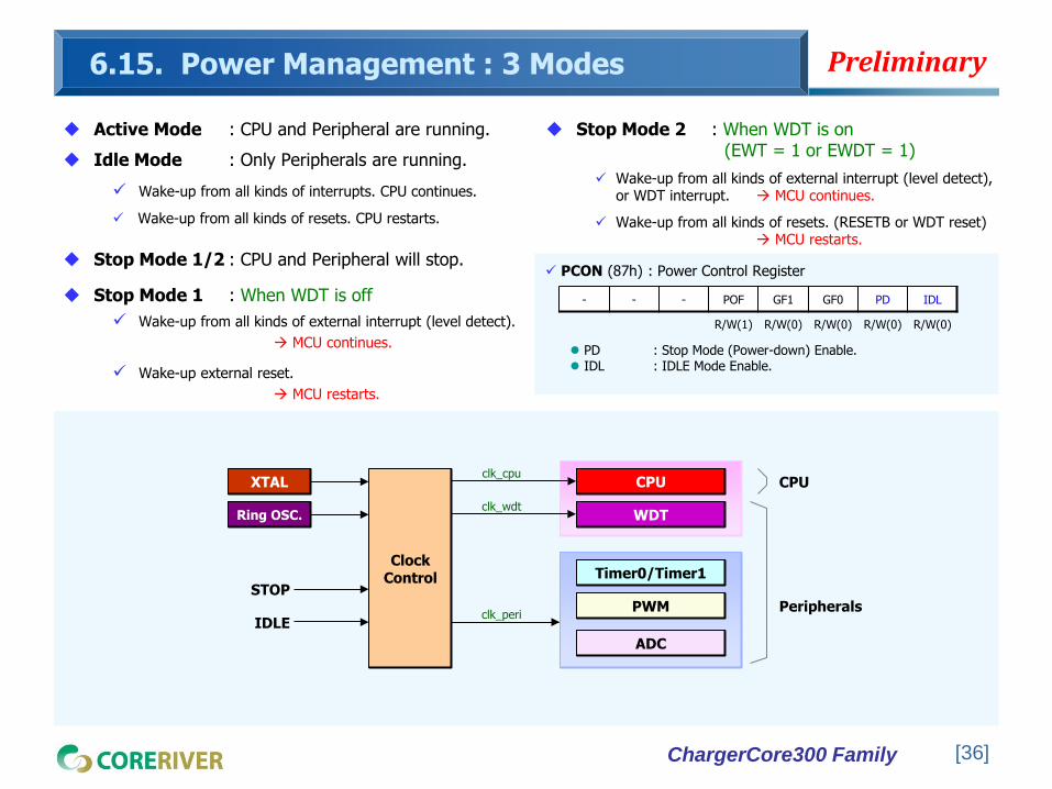
6.15. Power Management : 3 Modes
Active Mode : CPU and Peripheral are running.
Idle Mode : Only Peripherals are running.
Wake-up from all kinds of interrupts. CPU continues.
Wake-up from all kinds of resets. CPU restarts.
Stop Mode 1/2 : CPU and Peripheral will stop.
Stop Mode 1 : When WDT is off
Wake-up from all kinds of external interrupt (level detect).
MCU continues.
Wake-up external reset.
MCU restarts.
Stop Mode 2 : When WDT is on (EWT = 1 or EWDT = 1)
Wake-up from all kinds of external interrupt (level detect), or WDT interrupt. MCU continues.
Wake-up from all kinds of resets. (RESETB or WDT reset) MCU restarts.
- - - POF GF1 GF0 PD IDL
R/W(1) R/W(0) R/W(0) R/W(0) R/W(0)
PCON (87h) : Power Control Register
PD : Stop Mode (Power-down) Enable. IDL : IDLE Mode Enable.
CPU
WDT
Timer0/Timer1
PWM
ADC
clk_cpu
clk_wdt
clk_peri
XTAL
Ring OSC.
STOP
IDLE
Peripherals
CPU
Clock Control

ChargerCore300 Family
Preliminary
[37]
6.16. ISP (In System Programming)
Code memory (2kBytes) can be programmed using EJTAG in target system.
FLASH : 0x0000 ~ 0x07FF (2,048 Bytes)
EEPROM (128Bytes) can be programmed using EJTAG in target system.
EEPROM : 0x0780 ~ 0x07FF (128 Bytes)
Target System
User’s PC
EJTAG Port
MCU
GenICE3000 Equipment
MDS Bridge
VCC
VSS
RESETB
ISP_SCL (P0.1)
[ISP Pin Configuration ]
ISP_SDA (P0.2)
ChargerCore300 Family
Preliminary
[38]
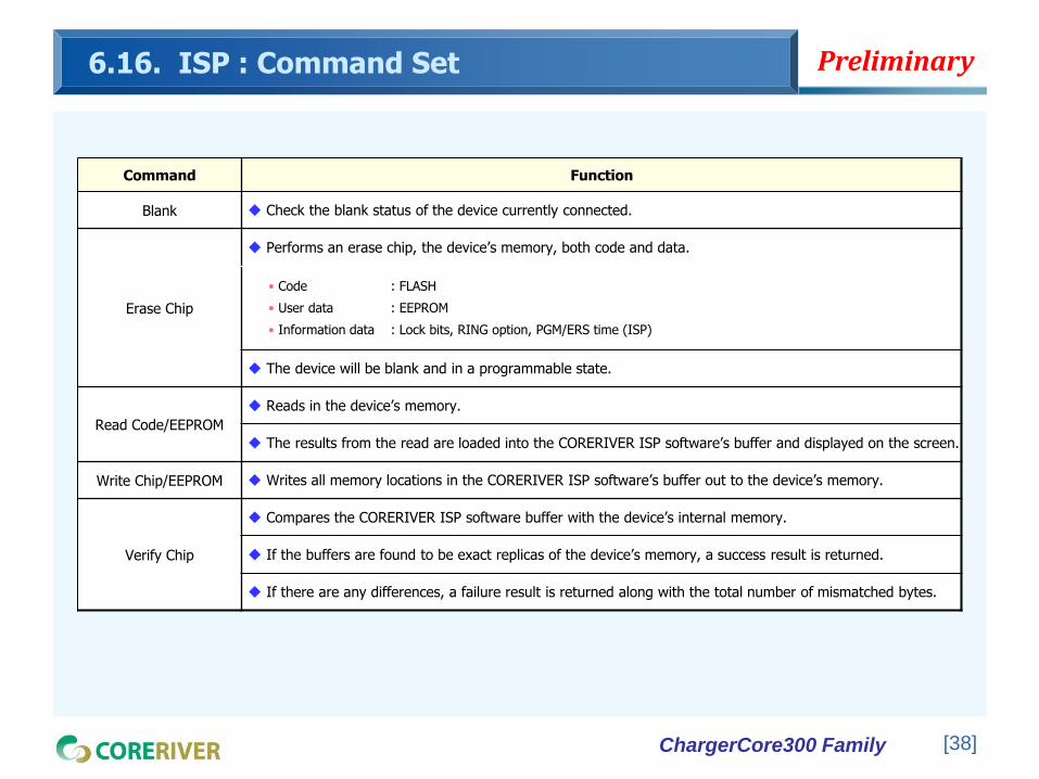
6.16. ISP : Command Set
Command Function
Blank Check the blank status of the device currently connected.
Erase Chip
Performs an erase chip, the device’s memory, both code and data.
• Code : FLASH
• User data : EEPROM
• Information data : Lock bits, RING option, PGM/ERS time (ISP)
The device will be blank and in a programmable state.
Read Code/EEPROM
Reads in the device’s memory.
The results from the read are loaded into the CORERIVER ISP software’s buffer and displayed on the screen.
Write Chip/EEPROM Writes all memory locations in the CORERIVER ISP software’s buffer out to the device’s memory.
Verify Chip
Compares the CORERIVER ISP software buffer with the device’s internal memory.
If the buffers are found to be exact replicas of the device’s memory, a success result is returned.
If there are any differences, a failure result is returned along with the total number of mismatched bytes.
ChargerCore300 Family
Preliminary
[39]
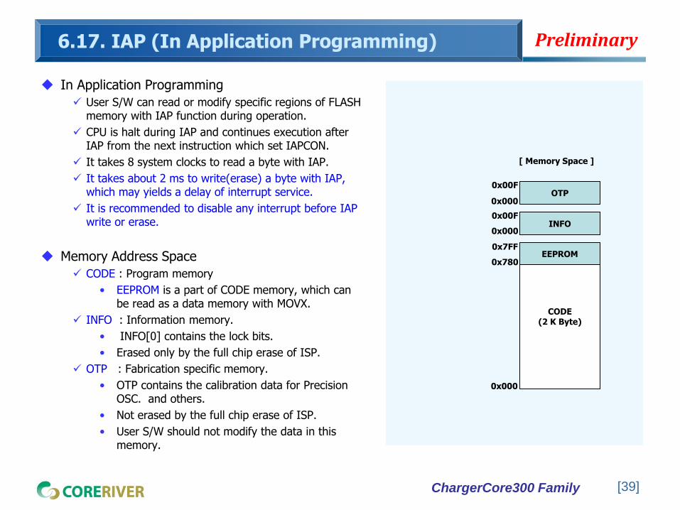
6.17. IAP (In Application Programming)
In Application Programming
User S/W can read or modify specific regions of FLASH memory with IAP function during operation.
CPU is halt during IAP and continues execution after IAP from the next instruction which set IAPCON.
It takes 8 system clocks to read a byte with IAP.
It takes about 2 ms to write(erase) a byte with IAP, which may yields a delay of interrupt service.
It is recommended to disable any interrupt before IAP write or erase.
Memory Address Space
CODE : Program memory
• EEPROM is a part of CODE memory, which can be read as a data memory with MOVX.
INFO : Information memory.
• INFO[0] contains the lock bits.
• Erased only by the full chip erase of ISP.
OTP : Fabrication specific memory.
• OTP contains the calibration data for Precision OSC. and others.
• Not erased by the full chip erase of ISP.
• User S/W should not modify the data in this memory.
OTP
CODE (2 K Byte)
0x000
EEPROM 0x780
0x7FF
0x000
0x00F
0x00F
0x000
INFO
[ Memory Space ]

ChargerCore300 Family
Preliminary 6.17. IAP (In Application Programming)
IAP Related SFR
DPH / DPL : Address for IAP.
IAPDAT: 8-bit data buffer for read or write by IAP.
IAPCON : IAP control SFR. Automatically cleared to zero after IAP is done.
IAPWEN : A protection code (0xAC35) should be written to this address to enable IAP write(erase).
[40]
WEN.7 WEN.6 WEN.5 WEN.4 WEN.3 WEN.2 WEN.1 WEN.0
R/W(0) R/W(0) R/W(0) R/W(0) R/W(0) R/W(0) R/W(0) R/W(0)
IAPWEN (FCh) : IAP Write/Erase Enable Register
DPL.7 DPL.6 DPL.5 DPL.4 DPL.3 DPL.2 DPL.1 DPL.0
R/W(0) R/W(0) R/W(0) R/W(0) R/W(0) R/W(0) R/W(0) R/W(0)
DPL (82h) : Data Pointer Low Register
DPH.7 DPH.6 DPH.5 DPH.4 DPH.3 DPH.2 DPH.1 DPH.0
R/W(0) R/W(0) R/W(0) R/W(0) R/W(0) R/W(0) R/W(0) R/W(0)
DPH (83h) : Data Pointer High Register
- - - - RGS1 RGS0 OPS1 OPS0
R/W(0) R/W(0) R/W(0) R/W(0) R/W(0) R/W(0) R/W(0) R/W(0)
IAPCON (FDh) : IAP Control SFR
DAT.7 DAT.6 DAT.5 DAT.4 DAT.3 DAT.2 DAT.1 DAT.0
R/W(0) R/W(0) R/W(0) R/W(0) R/W(0) R/W(0) R/W(0) R/W(0)
IAPDAT (FEh) : IAP read/write Data Register RGS1 RGS0 IAP Region
0 0 CODE (0x000 ~ 0x7FF)
0 1 Reserved
1 0 INFO (0x0 ~ 0xF)
1 1 OTP (0x0 ~ 0xF)
RGS[1:0] : Select IAP region
OPS1 OPS0 IAP Function
0 0 No operation
0 1 Byte Read : IAPDAT = F[DPTR]
1 0 Byte Erase : F[DPTR] = 0
1 1 Byte Write : F[DPTR] = IAPDAT
OPS[1:0] : Select IAP function

ChargerCore300 Family
Preliminary
[41]
6.17. IAP (In Application Programming)
Electrical Characteristic of IAP
Note that the program time depends on the frequency of CPU clock.
If the clock frequency is out of IAP range, user should use the internal RING clock for IAP write.
Parameter Symbol MIN TYP MAX Unit
Power Supply
Voltage
VDD 2.7 3.3 5.5 V
CPU Clock
Frequency FSYS 3 4 5 MHz
Write / Erase
Time Tp 1.5 2.0 3.3 ms
Enable condition of IAP write(erase)
The protection code (0xAC35) should be written to 16-bit hidden write enable register through IAPWEN.
- - - - - - - LB0
Lock Bits (The first byte of INFO memory)
LB0 : If set, disable ISP except the full chip erase.
ChargerCore300 Family
Preliminary 6.17. IAP (In Application Programming)
[42]
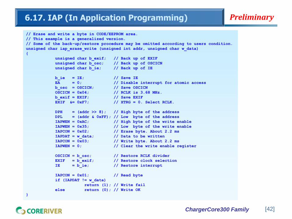
// Erase and write a byte in CODE/EEPROM area.
// This example is a generalized version.
// Some of the back-up/restore procedure may be omitted according to users condition.
unsigned char iap_erase_write (unsigned int addr, unsigned char w_data)
unsigned char b_exif; // Back up of EXIF
unsigned char b_osc; // Back up of OSCICN
unsigned char b_ie; // Back up of IE
b_ie = IE; // Save IE
EA = 0; // Disable interrupt for atomic access
b_osc = OSCICN; // Save OSCICN
OSCICN = 0x04; // RCLK is 3.68 MHz.
b_exif = EXIF; // Save EXIF
EXIF &= 0xF7; // XTRG = 0. Select RCLK.
DPH = (addr >> 8); // High byte of the address
DPL = (addr & 0xFF); // Low byte of the address
IAPWEN = 0xAC; // High byte of the write enable
IAPWEN = 0x35; // Low byte of the write enable
IAPCON = 0x02; // Erase byte. About 2.2 ms
IAPDAT = w_data; // Data to be written
IAPCON = 0x03; // Write byte. About 2.2 ms
IAPWEN = 0; // Clear the write enable register
OSCICN = b_osc; // Restore RCLK divider
EXIF = b_exif; // Restore clock selection
IE = b_ie; // Restore interrupt
IAPCON = 0x01; // Read byte
if (IAPDAT != w_data)
return (1); // Write fail
else return (0); // Write OK
ChargerCore300 Family
Preliminary
[43]
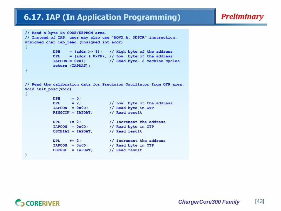
6.17. IAP (In Application Programming)
// Read a byte in CODE/EEPROM area.
// Instead of IAP, user may also use “MOVX A, @DPTR” instruction.
unsigned char iap_read (unsigned int addr)
DPH = (addr >> 8); // High byte of the address
DPL = (addr & 0xFF); // Low byte of the address
IAPCON = 0x01; // Read byte. 2 machine cycles
return (IAPDAT);
// Read the calibration data for Precision Oscillator from OTP area.
void init_posc(void)
DPH = 0;
DPL = 2; // Low byte of the address
IAPCON = 0x0D; // Read byte in OTP
RINGCON = IAPDAT; // Read result
DPL += 2; // Increment the address
IAPCON = 0x0D; // Read byte in OTP
OSCBIAS = IAPDAT; // Read result
DPL += 2; // Increment the address
IAPCON = 0x0D; // Read byte in OTP
OSCREF = IAPDAT; // Read result

ChargerCore300 Family
Preliminary
[44]
7. Absolute Maximum Ratings
Items Conditions Ranges
Voltage on any pin relative to Ground - -0.5V to (VDD+0.5V)
Voltage in VDD relative to Ground - -0.5V to 6.5V
Output Voltage - -0.5V to (VDD+0.5V)
Output Current High
One I/O pin active -25mA
All I/O pin active -100mA
Output Current Low
One I/O pin active +30mA
All I/O pin active +150mA
Storage Temperature - -65 oC to +150 oC
Soldering Temperature - 260 oC for 10 seconds
ChargerCore300 Family
Preliminary
[45]
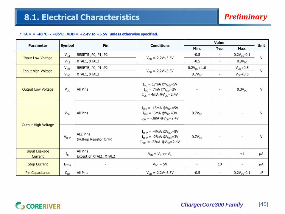
8.1. Electrical Characteristics
* TA = = -40 °C ~ +85°C , VDD = +2.4V to +5.5V unless otherwise specified.
Parameter Symbol Pin Conditions Value
Unit Min. Typ. Max.
Input Low Voltage VIL1 RESETB ,P0, P1, P2
VDD = 2.2V~5.5V -0.5 - 0.2VDD-0.1
V VIL2 XTAL1, XTAL2 -0.5 - 0.3VDD
Input high Voltage VIH1 RESETB, P0, P1 ,P2
VDD = 2.2V~5.5V 0.2VDD+1.0 - VDD+0.5
V VIH2 XTAL1, XTAL2 0.7VDD - VDD+0.5
Output Low Voltage VOL All Pins
IOL = 17mA @VDD=5V
IOL = 7mA @VDD=3V
IOL = 4mA @VDD=2.4V
- - 0.3VDD V
Output High Voltage
VOH All Pins
IOH = -18mA @VDD=5V
IOH = -6mA @VDD=3V
IOH = -3mA @VDD=2.4V
0.7VDD - - V
VOHP
ALL Pins
(Pull-up Resistor Only)
IOHP = -49uA @VDD=5V
IOHP = -28uA @VDD=3V
IOHP = -22uA @VDD=2.4V
0.7VDD - - V
Input Leakage
Current IIL
All Pins
Except of XTAL1, XTAL2 VIN = VIH or VIL - - ±1 A
Stop Current ISTOP - VDD = 5V - 10 - A
Pin Capacitance CIO All Pins VDD = 2.2V~5.5V -0.5 - 0.2VDD-0.1 pF

ChargerCore300 Family
Preliminary 8.2. Electrical Characteristics
[46]
* TA = = -40 °C ~ +85°C , VDD = +4.5V to +5.5V unless otherwise specified.
Symbol Parameter Conditions Value
Unit Min. Typ. Max.
ACIN INPUT CURRENT AND POWER-ON-RESET (POR)
IACIN ACIN Supply Current IOUT = 0A, ICHRIN = 0A 300 350
VPOR ACIN POR Threshold VACIN rising 2 3 V
ACIN POR Hysteresis 200 250 300
TB(ACIN) ACIN Power-On Blanking Time 8
INTERNAL SWITCH ON RESISTANCE
CHRIN Discharge On Resistance 500 Ω
INPUT OVER-VOLTAGE PROTECTION (OVP)
VOVP Input OVP Threshold VACIN rising 6 6.17 6.35 V
Input OVP Hysteresis 200 300 400
Input OVP Propagation Delay 1
TON(OVP) Input OVP Recovery Time 8
OVER-VOLTAGE PROTECTION (OCP)
IOCP OCP Threshold 1 1.5 A
OCP Blanking Time 176
TON(OCP) OCP Recovery Time 64
INTERNAL P-MOSFET (CHRIN)
P-MOSFET Input Capacitance 100 Ω
OVER-TEMPERATURE PROTECTION (OTP)
TOTP Over-Temperature Threshold TJ rising 160
Over-Temperature Hysteresis 40

ChargerCore300 Family
Preliminary
[47]
9. AC Characteristics
* TA = -40 oC ~ +85 oC unless otherwise specified.
External Interrupt Pin
RESETB 0.2VDD 0.2VDD
tRST
0.8VDD 0.8VDD
0.2VDD 0.2VDD
tINT
tINT
Parameter Symbol Pin Conditions Value
Unit Min. Typ. Max.
Operating Frequency FSYS
Internal Oscillator
XTAL1, XTAL2
VDD = 5V ± 10% 1 - 12 MHz
VDD = 3V ± 10% 1 - 12
RESETB Input Width tRST RESETB VDD = 5V ± 10% 24 - -
FSYS VDD = 3V ± 10% 24 - -
External Interrupt
Input Width tINT External Interrupt
VDD = 5V ± 10% 4 - - FSYS
VDD = 3V ± 10% 4 - -

ChargerCore300 Family
Preliminary
[48]
10. ADC Specifications
Parameter Symbol Conditions
Value
Unit
Min. Typ. Max.
Supply Voltage VDDADC - 1.6 - 5.5 V
Input Voltage VINADC - VSS - VDD V
Resolution RESADC - - 10 - bit
Operating Frequency FADC VDD = 4.5V ~ 5.5V
VDD = 2.4V ~ 3.3V - -
10
5 MHz
Conversion Time tADC - - 96 / FADC - s
Overall Accuracy OAADC
VDD =5V, FADC=10MHz
VDD =3V, FADC=5MHz - ±2 ±4 LSB
Integral Nonlinearity INLADC
VDD =5V, FADC=10MHz
VDD =3V, FADC=5MHz - ±2 ±4 LSB
Differential Nonlinearity DNLADC
VDD =5V, FADC=10MHz
VDD =3V, FADC=5MHz - ±0.5 ±1 LSB
Zero Input Error ZIEADC
VDD =5V, FADC=10MHz
VDD =3V, FADC=5MHz - ±2 ±4 LSB
Full Scale Error FSEADC
VDD =5V, FADC=10MHz
VDD =3V, FADC=5MHz - ±2 ±4 LSB
Analog Input Capacitance CINADC - - 10 15 pF
ADC
Current
Active
IADC
VDD = 5V, FADC=10MHz - 1 2
mA
VDD = 3V, FADC=5MHz - 0.3 0.6
Power-down VDD = 5V - - 100 nA
ChargerCore300 Family
Preliminary
[49]
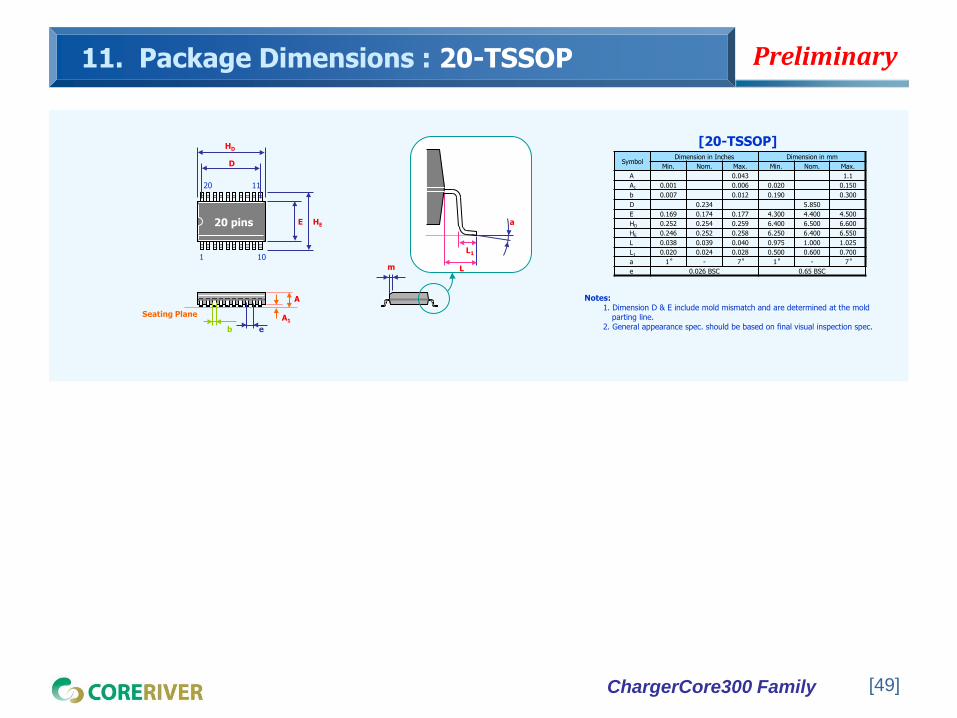
11. Package Dimensions : 20-TSSOP
A
m
Symbol Dimension in Inches Dimension in mm
Min. Nom. Max. Min. Nom. Max.
A 0.043 1.1
A1 0.001 0.006 0.020 0.150
b 0.007 0.012 0.190 0.300
D 0.234 5.850
E 0.169 0.174 0.177 4.300 4.400 4.500
HD 0.252 0.254 0.259 6.400 6.500 6.600
HE 0.246 0.252 0.258 6.250 6.400 6.550
L 0.038 0.039 0.040 0.975 1.000 1.025
L1 0.020 0.024 0.028 0.500 0.600 0.700
a 1 - 7 1 - 7
e 0.026 BSC 0.65 BSC
Notes: 1. Dimension D & E include mold mismatch and are determined at the mold parting line. 2. General appearance spec. should be based on final visual inspection spec. b e
A1 Seating Plane
a
L
L1
[20-TSSOP]
20 pins
1
20 11
10
HD
E
D
HE

ChargerCore300 Family
Preliminary
[50]
12. Supporting tools
In-Circuit Debugger (GENSYS & GenICE)
World Wide Programmable in Anywhere (Hi-Lo Systems, ADVANTECH, TOPMAX, CORERIVER)
Support Parallel / Serial Programming
ROM Writer
Easy-to-Use GUI (GENTOS)
Assembler & Linker for Windows Optimized Cross-C Compiler
On-board Application (with MCU Demo) Various Sample Test Program
Application System
ChargerCore300 Family
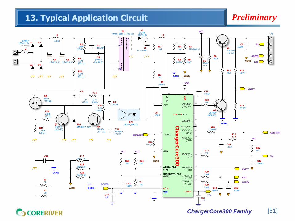
Preliminary 13. Typical Application Circuit
[51]
VCCVCC
1N4007(DO-41_R)
(x 4pcs)
C34.7uF/400V
330uH
L1
D1 D3
D2 D4
F1
R31.5M(2012)
R111.5M(2012)
R1100k
(2012)
C1102/1kV
D51N4007
(DO-41_R)
8
7
6
5
Q21N60(TO251)
2
3
1
R191.5R/F(2012)
R14220R(2012)
Q32N3904(SOT-23)
ZD1ZMM5237-8.2V
C9
1nF(2012)
3
1
2 2
3
1 Q42N3904(SOT-23)
R12
1.5k(2012)
R151.3k
(2012)
D7LL4148
C1047nF/X7R(2012)
T1TRANS_EE1616_PTC-750
1
2
3
4
4
3
1
2
PC1PC17K_PHOTO
D6SR240
(DO-15_R)
C44.7uF/400V
C5680uF/10V
L2
R210R
R410k/F
C2100nF
R1012k/F
R13270k/F
R21330R
AGND
DGND
VBATT
R86.19k/F
R52M (Option)
R912k/F
C6220uF/10V
R6510R
AGNDDGND
VCC
ID
GREEN
RED
VCTRL
16
13OUT
R72k
18VSENSE
C7100nF
C8100nF
14GND
R16150R/F
AGND
VD
D
20
VC
C
17
R171R (3216)
R181R (3216)
R203R (3216)
AGND DGND
DGND
C17
J10R
J20R
11ADC1/P0.2
R3210k
Q52N3904
(SOT-23)
3
1
2
1 2
3 Q1KSA928A(TO-92)
R2733k
8ADC8/P2.5 ID
7ADC9/P2.4 VBATT
R2210k
VCC
3XTAL2/P1.1 RED
2XTAL1/P1.0 GREEN
C14100nF
C15100nF
R29330R
R29330R
CURRENT
10ADC3/P0.4
9ADC4/P0.5
15ICTRL
1VSS
CURRENT
R23270R/F
R2533k
C16100nF
C12100nF
C11100nF
5ADC11/P2.2
4RESETB/VPP/P1.2
C13100nF
R2410k
R2610k
TH10k
VCC VCC
Ch
arg
erC
ore
2.0
5
1
2
3
4
CN1
(ON_OFF)
(ID)
(B+)
(R_LED)
(G_LED)
(ID_S)
(CUR)
(TP)
(RES)
12ADC1/P0.1
19P0.0
6ADC10/P2.3
3
ADC5/P0.6 (ID)
Ch
arg
erC
ore
30
0
VD
D
VCC P0.0
VCTRL
OUT
VSENSE
GND
ADC11/P2.2 (TP)
RESET/VPP/P1.2 (RES)
XTAL1/P1.0 (G_LED)
XTAL2/P1.1 (R_LED)
ADC1/P0.2 (ON_OFF)
ADC0/P0.1
ADC10/P2.3
ADC3/P0.4 (ID_S)
ADC4/P0.5 (CUR)
ADC5/P0.6 (ID)
ADC2/P0.3 (B+)
VSS
C40 1uF
ACIN
CHRIN
C41 1uF
POWER
VCC

ChargerCore300 Family
Preliminary
[52]
Appendix A : Instruction Set (1/19)
Note on Instruction Set and Addressing Modes
Notation Descriptions
Rn Register R0 ~ R7 of the currently selected Register Bank (RB0 ~ RB3).
direct The address of 8-bit internal data location.
This could be an IRAM location (0x00 ~ 0x7F; 128 bytes) or a SFR (0x80 ~ 0xFF).
@Ri 8-bit IRAM location (0x00 ~ 0xFF; 256 bytes) addressed indirectly through register R0 or R1.
#data 8-bit constant included in instruction.
#data16 16-bit constant included in instruction.
addr16
16-bit destination address.
Used by LCALL & LJMP. The branch can be anywhere within the 64kbytes program memory address
space. (ChargerCore300 Family : 2kbytes program memory)
addr11
11-bit destination address.
Used by ACALL & AJMP. The branch will be within the same 2kbytes page of program memory as the
first byte of the following instruction.
rel
Signed (2’s complement number) 8-bit offset byte.
Used by SJMP and all conditional jumps. Range is -128 to +127 byte relative to first byte of the
following instruction.
Bit Direct addressed bit n IRAM of SFR.
ChargerCore300 Family
Preliminary
[53]
Appendix A : Instruction Set (2/19)
1 cycle = 4 clocks
ADD A, Rn
Operation : (A) (A) + (Rn)
ADD A, @Ri
Operation : (A) (A) + ((Ri))
ADD A, direct
Operation : (A) (A) + (direct)
ADD A, #date
Operation : (A) (A) + data
Encoding : HEX: 28h, #bytes: 1, Cycles: 1
0 0 1 0 1 r r r
Encoding : HEX: 26h, #bytes: 1, Cycles: 1
0 0 1 0 0 1 1 i
Encoding : HEX: 25h, #bytes: 2, Cycles: 2
0 0 1 0 0 1 0 1 direct addr
Encoding : HEX: 24h, #bytes: 2, Cycles: 2
0 0 1 0 0 1 0 0 immediate data
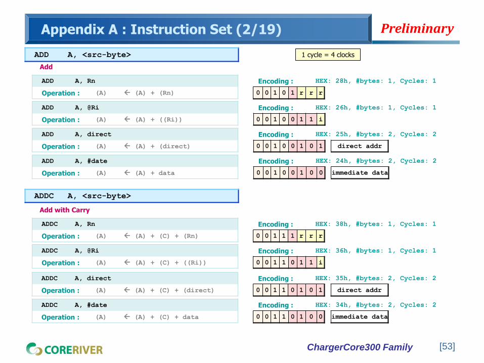
ADD A, <src-byte>
ADDC A, <src-byte>
Add
ADDC A, Rn
Operation : (A) (A) + (C) + (Rn)
ADDC A, @Ri
Operation : (A) (A) + (C) + ((Ri))
Encoding : HEX: 38h, #bytes: 1, Cycles: 1
0 0 1 1 1 r r r
Encoding : HEX: 36h, #bytes: 1, Cycles: 1
0 0 1 1 0 1 1 i
Add with Carry
ADDC A, direct
Operation : (A) (A) + (C) + (direct)
ADDC A, #date
Operation : (A) (A) + (C) + data
Encoding : HEX: 35h, #bytes: 2, Cycles: 2
0 0 1 1 0 1 0 1 direct addr
Encoding : HEX: 34h, #bytes: 2, Cycles: 2
0 0 1 1 0 1 0 0 immediate data

ChargerCore300 Family
Preliminary
[54]
Appendix A : Instruction Set (3/19)
SUBB A, <src-byte>
SUBB A, Rn
Operation : (A) (A) - (C) - (Rn)
SUBB A, @Ri
Operation : (A) (A) - (C) - ((Ri))
Encoding : HEX: 98h, #bytes: 1, Cycles: 1
1 0 0 1 1 r r r
Encoding : HEX: 96h, #bytes: 1, Cycles: 1
1 0 0 1 0 1 1 i
Subtract with Borrow
SUBB A, direct
Operation : (A) (A) - (C) - (direct)
SUBB A, #date
Operation : (A) (A) - (C) - data
Encoding : HEX: 95h, #bytes: 2, Cycles: 2
1 0 0 1 0 1 0 1 direct addr
Encoding : HEX: 94h, #bytes: 2, Cycles: 2
1 0 0 1 0 1 0 0 immediate data
INC <byte>
INC A
Operation : (A) (A) + 1
INC Rn
Operation : (Rn) (Rn) + 1
Encoding : HEX: 04h, #bytes: 1, Cycles: 1
0 0 0 0 0 1 0 0
Encoding : HEX: 08h, #bytes: 1, Cycles: 1
0 0 0 0 1 r r r
Increment
INC @Ri
Operation : ((Ri)) ((Ri)) + 1
INC direct
Operation : (direct) (direct) + 1
Encoding : HEX: 05h, #bytes: 2, Cycles: 2
0 0 0 0 0 1 0 1 direct addr
Encoding : HEX: 06h, #bytes: 1, Cycles: 1
0 0 0 0 0 1 1 i
INC DPTR
Operation : (DPTR) (DPTR) + 1
Encoding : HEX: A3h, #bytes: 1, Cycles: 1
1 0 1 0 0 0 1 1

ChargerCore300 Family
Preliminary
[55]
Appendix A : Instruction Set (4/19)
DEC <byte>
DEC A
Operation : (A) (A) - 1
DEC Rn
Operation : (Rn) (Rn) - 1
Encoding : HEX: 14h, #bytes: 1, Cycles: 1
0 0 0 1 0 1 0 0
Encoding : HEX: 18h, #bytes: 1, Cycles: 1
0 0 0 1 1 r r r
Decrement
DEC @Ri
Operation : ((Ri)) ((Ri)) - 1
DEC direct
Operation : (direct) (direct) - 1
Encoding : HEX: 15h, #bytes: 1, Cycles: 1
0 0 0 1 0 1 0 1 direct addr
Encoding : HEX: 16h, #bytes: 1, Cycles: 1
0 0 0 1 0 1 1 i
MUL AB
Operation : (A)7-0 (A) x (B)
(B)15-8
Encoding : HEX: A4h, #bytes: 1, Cycles: 3
1 0 1 0 0 1 0 0
Multiply
DIV AB
Operation : (A)15-8 (A) / (B)
(B)7-0
Encoding : HEX: 84h, #bytes: 1, Cycles: 3
1 0 0 0 0 1 0 0
Divide

ChargerCore300 Family
Preliminary
[56]
Appendix A : Instruction Set (5/19)
DA A
Operation :
IF [[(A3-0)>9] [(AC)=1]]
THEN (A3-0) (A3-0)+6
IF [[(A7-4)>9] [(C)=1]]
THEN (A7-4) (A7-4)+6
Encoding : HEX: D4h, #bytes: 1, Cycles: 1
1 1 0 1 0 1 0 0
Decimal-adjust Accumulator for Addition
ANL A, Rn
Operation : (A) (A) ^ (Rn)
ANL A, @Ri
Operation : (A) (A) ^ ((Ri))
ANL A, direct
Operation : (A) (A) ^ (direct)
ANL A, #date
Operation : (A) (A) ^ data
Encoding : HEX: 58h, #bytes: 1, Cycles: 1
0 1 0 1 1 r r r
Encoding : HEX: 56h, #bytes: 1, Cycles: 1
0 1 0 1 0 1 1 i
Encoding : HEX: 55h, #bytes: 2, Cycles: 2
0 1 0 1 0 1 0 1 direct addr
Encoding : HEX: 54h, #bytes: 2, Cycles: 2
0 1 0 1 0 1 0 0 immediate data
ANL <dest-byte>, <src-byte>
Logical AND for byte variables
ANL direct, A
Operation : (direct) (direct) ^ (A)
Encoding : HEX: 52h, #bytes: 2, Cycles: 2
0 1 0 1 0 0 1 0 direct addr
Encoding : HEX: 53h, #bytes: 3, Cycles: 3
0 1 0 1 0 0 1 1 direct addr immediate data
ANL direct, #data
Operation : (direct) (direct) ^ data

ChargerCore300 Family
Preliminary
[57]
Appendix A : Instruction Set (6/19)
ANL C, bit
Operation : (C) (C) ^ (bit)
Encoding : HEX: 82h, #bytes: 2, Cycles: 2
1 0 0 0 0 0 1 0 bit addr
ANL C, <src-bit>
Logical AND for bit variables
ANL C, /bit
Operation : (C) (C) ^ ~(bit)
Encoding : HEX: B0h, #bytes: 2, Cycles: 2
1 0 1 1 0 0 0 0 bit addr
ORL A, Rn
Operation : (A) (A) (Rn)
ORL A, @Ri
Operation : (A) (A) ((Ri))
ORL A, direct
Operation : (A) (A) (direct)
ORL A, #date
Operation : (A) (A) data
Encoding : HEX: 48h, #bytes: 1, Cycles: 1
0 1 0 0 1 r r r
Encoding : HEX: 46h, #bytes: 1, Cycles: 1
0 1 0 0 0 1 1 i
Encoding : HEX: 45h, #bytes: 2, Cycles: 2
0 1 0 0 0 1 0 1 direct addr
Encoding : HEX: 44h, #bytes: 2, Cycles: 2
0 1 0 0 0 1 0 0 immediate data
ORL <dest-byte>, <src-byte>
Logical OR for byte variables
ORL direct, A
Operation : (direct) (direct) (A)
Encoding : HEX: 42h, #bytes: 2, Cycles: 2
0 1 0 0 0 0 1 0 direct addr
Encoding : HEX: 43h, #bytes: 3, Cycles: 3
0 1 0 0 0 0 1 1 direct addr immediate data
ORL direct, #data
Operation : (direct) (direct) data
ChargerCore300 Family
Preliminary
[58]
Appendix A : Instruction Set (7/19)
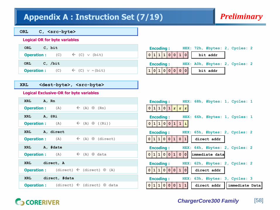
ORL C, bit
Operation : (C) (C) (bit)
Encoding : HEX: 72h, #bytes: 2, Cycles: 2
0 1 1 1 0 0 1 0 bit addr
ORL C, <src-byte>
Logical OR for byte variables
ORL C, /bit
Operation : (C) (C) ~(bit)
Encoding : HEX: A0h, #bytes: 2, Cycles: 2
1 0 1 0 0 0 0 0 bit addr
XRL A, Rn
Operation : (A) (A) (Rn)
XRL A, @Ri
Operation : (A) (A) ((Ri))
XRL A, direct
Operation : (A) (A) (direct)
XRL A, #date
Operation : (A) (A) data
Encoding : HEX: 68h, #bytes: 1, Cycles: 1
0 1 1 0 1 r r r
Encoding : HEX: 66h, #bytes: 1, Cycles: 1
0 1 1 0 0 1 1 i
Encoding : HEX: 65h, #bytes: 2, Cycles: 2
0 1 1 0 0 1 0 1 direct addr
Encoding : HEX: 64h, #bytes: 2, Cycles: 2
0 1 1 0 0 1 0 0 immediate data
XRL <dest-byte>, <src-byte>
Logical Exclusive-OR for byte variables
XRL direct, A
Operation : (direct) (direct) (A)
Encoding : HEX: 62h, #bytes: 2, Cycles: 2
0 1 1 0 0 0 1 0 direct addr
Encoding : HEX: 63h, #bytes: 3, Cycles: 3
0 1 1 0 0 0 1 1 direct addr immediate Data
XRL direct, #data
Operation : (direct) (direct) data

ChargerCore300 Family
Preliminary
[59]
Appendix A : Instruction Set (8/19)
CLR A
Operation : (A) 0
Encoding : HEX: E4h, #bytes: 1, Cycles: 1
1 1 1 0 0 1 0 0
Clear Accumulator
CLR <bit>
CLR C
Operation : (C) 0
Encoding : HEX: C3h, #bytes: 1, Cycles: 1
1 1 0 0 0 0 1 1
Clear bit
CLR bit
Operation : (bit) 0
Encoding : HEX: C2h, #bytes: 2, Cycles: 2
1 1 0 0 0 0 1 0 bit addr
CPL A
Operation : (A) ~(A)
Encoding : HEX: F4h, #bytes: 1, Cycles: 1
1 1 1 1 0 1 0 0
Complement Accumulator
CPL <bit>
CPL C
Operation : (C) ~(C)
Encoding : HEX: B3h, #bytes: 1, Cycles: 1
1 0 1 1 0 0 1 1
Complement bit
CPL bit
Operation : (bit) ~(bit)
Encoding : HEX: B2h, #bytes: 2, Cycles: 2
1 0 1 1 0 0 1 0 bit addr

ChargerCore300 Family
Preliminary
[60]
Appendix A : Instruction Set (9/19)
RL A
Operation : (An+1) (An) n=0~6
(A0) (A7)
Encoding : HEX: 23h, #bytes: 1, Cycles: 1
0 0 1 0 0 0 1 1
Rotate Accumulator Left
RLC A
Operation :
(An+1) (An) n=0~6
(A0) (C)
(C) (A7)
Encoding : HEX: 33h, #bytes: 1, Cycles: 1
0 0 1 1 0 0 1 1
Rotate Accumulator Left through the Carry flag
RR A
Operation : (An) (An+1) n=0~6
(A7) (A0)
Encoding : HEX: 03h, #bytes: 1, Cycles: 1
0 0 0 0 0 0 1 1
Rotate Accumulator Right
RRC A
Operation :
(An) (An+1) n=0~6
(A7) (C)
(C) (A0)
Encoding : HEX: 13h, #bytes: 1, Cycles: 1
0 0 0 1 0 0 1 1
Rotate Accumulator Right through the Carry flag
SWAP A
Operation : (A3-0) (A7-4)
Encoding : HEX: C4h, #bytes: 1, Cycles: 1
1 1 0 0 0 1 0 0
Swap nibbles within the Accumulator

ChargerCore300 Family
Preliminary
[61]
Appendix A : Instruction Set (10/19)
MOV A, Rn
Operation : (A) (Rn)
MOV A, @Ri
Operation : (A) ((Ri))
MOV A, direct
Operation : (A) (direct)
MOV A, #date
Operation : (A) data
Encoding : HEX: E8h, #bytes: 1, Cycles: 1
1 1 1 0 1 r r r
Encoding : HEX: E6h, #bytes: 1, Cycles: 1
1 1 1 0 0 1 1 i
Encoding : HEX: E5h, #bytes: 2, Cycles: 2
1 1 1 0 0 1 0 1 direct addr
Encoding : HEX: 74h, #bytes: 2, Cycles: 2
0 1 1 1 0 1 0 0 immediate data
MOV <dest-byte>, <src-byte>
Move byte variable
MOV Rn, A
Operation : (Rn) (A)
MOV Rn, direct
Operation : (Rn) (direct)
MOV Rn, #date
Operation : (Rn) data
Encoding : HEX: A8h, #bytes: 2, Cycles: 2
1 0 1 0 1 r r r direct addr
Encoding : HEX: 78h, #bytes: 2, Cycles: 2
0 1 1 1 1 r r r immediate data
Encoding : HEX: F8h, #bytes: 1, Cycles: 1
1 1 1 1 1 r r r
MOV direct, A
Operation : (direct) (A)
Encoding : HEX: F5h, #bytes: 2, Cycles: 2
1 1 1 1 0 1 0 1 direct addr
MOV direct, Rn
Operation : (direct) (Rn)
Encoding : HEX: 88h, #bytes: 2, Cycles: 2
1 0 0 0 1 r r r direct addr
ChargerCore300 Family
Preliminary
[62]
Appendix A : Instruction Set (11/19)
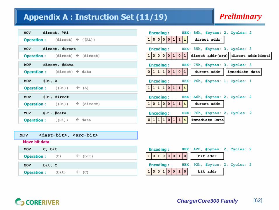
MOV direct, @Ri
Operation : (direct) ((Ri))
Encoding : HEX: 86h, #bytes: 2, Cycles: 2
1 0 0 0 0 1 1 i direct addr
Encoding : HEX: 85h, #bytes: 3, Cycles: 3
1 0 0 0 0 1 0 1 direct addr(src) direct addr(dest)
MOV direct, direct
Operation : (direct) (direct)
MOV direct, #data
Operation : (direct) data
Encoding : HEX: 75h, #bytes: 3, Cycles: 3
0 1 1 1 0 1 0 1 direct addr immediate data
MOV @Ri, A
Operation : ((Ri)) (A)
Encoding : HEX: F6h, #bytes: 1, Cycles: 1
1 1 1 1 0 1 1 i
MOV @Ri, direct
Operation : ((Ri)) (direct)
Encoding : HEX: A6h, #bytes: 2, Cycles: 2
1 0 1 0 0 1 1 i direct addr
MOV @Ri, #data
Operation : ((Ri)) data
Encoding : HEX: 76h, #bytes: 2, Cycles: 2
0 1 1 1 0 1 1 i immediate Data
MOV C, bit
Operation : (C) (bit)
MOV bit, C
Operation : (bit) (C)
Encoding : HEX: A2h, #bytes: 2, Cycles: 2
1 0 1 0 0 0 1 0 bit addr
Encoding : HEX: 92h, #bytes: 2, Cycles: 2
1 0 0 1 0 0 1 0 bit addr
MOV <dest-bit>, <src-bit>
Move bit data
ChargerCore300 Family
Preliminary
[63]
Appendix A : Instruction Set (12/19)
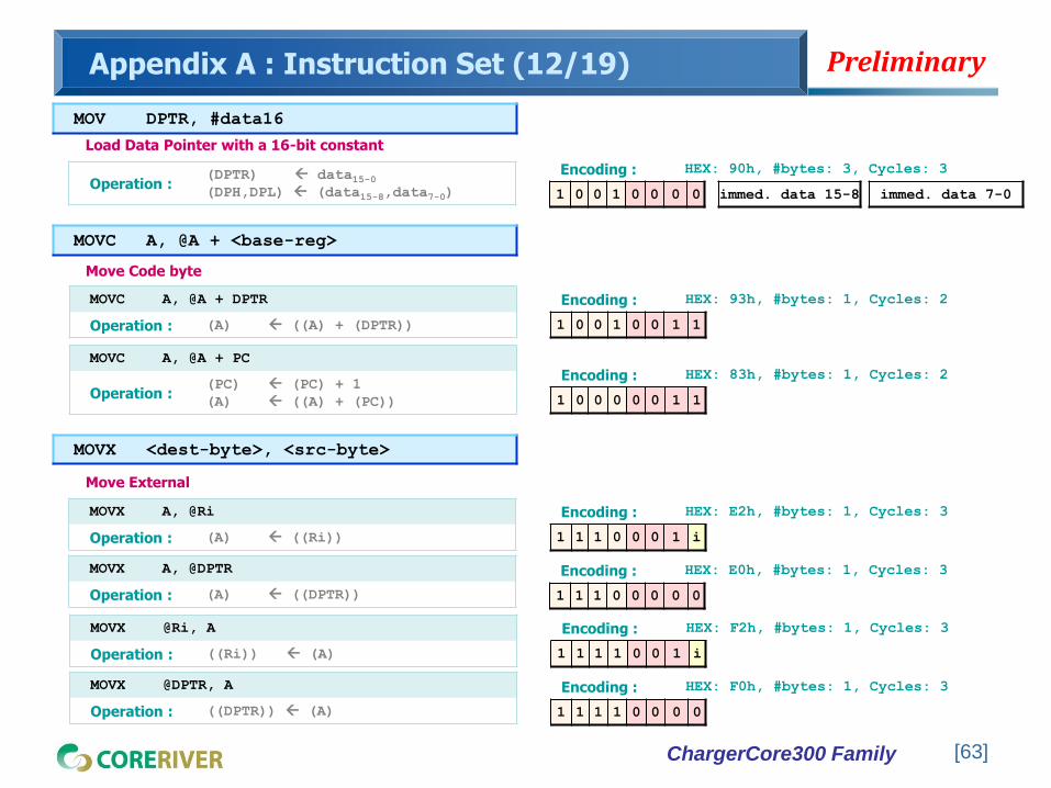
MOVC A, @A + DPTR
Operation : (A) ((A) + (DPTR))
MOVC A, @A + PC
Operation : (PC) (PC) + 1
(A) ((A) + (PC))
Encoding : HEX: 93h, #bytes: 1, Cycles: 2
1 0 0 1 0 0 1 1
Encoding : HEX: 83h, #bytes: 1, Cycles: 2
1 0 0 0 0 0 1 1
MOVC A, @A + <base-reg>
Move Code byte
MOV DPTR, #data16
Operation : (DPTR) data15-0 (DPH,DPL) (data15-8,data7-0)
Load Data Pointer with a 16-bit constant
Encoding : HEX: 90h, #bytes: 3, Cycles: 3
1 0 0 1 0 0 0 0 immed. data 15-8 immed. data 7-0
MOVX A, @DPTR
Operation : (A) ((DPTR))
MOVX A, @Ri
Operation : (A) ((Ri))
Encoding : HEX: E2h, #bytes: 1, Cycles: 3
1 1 1 0 0 0 1 i
MOVX <dest-byte>, <src-byte>
Move External
Encoding : HEX: E0h, #bytes: 1, Cycles: 3
1 1 1 0 0 0 0 0
MOVX @DPTR, A
Operation : ((DPTR)) (A)
MOVX @Ri, A
Operation : ((Ri)) (A)
Encoding : HEX: F2h, #bytes: 1, Cycles: 3
1 1 1 1 0 0 1 i
Encoding : HEX: F0h, #bytes: 1, Cycles: 3
1 1 1 1 0 0 0 0
ChargerCore300 Family
Preliminary
[64]
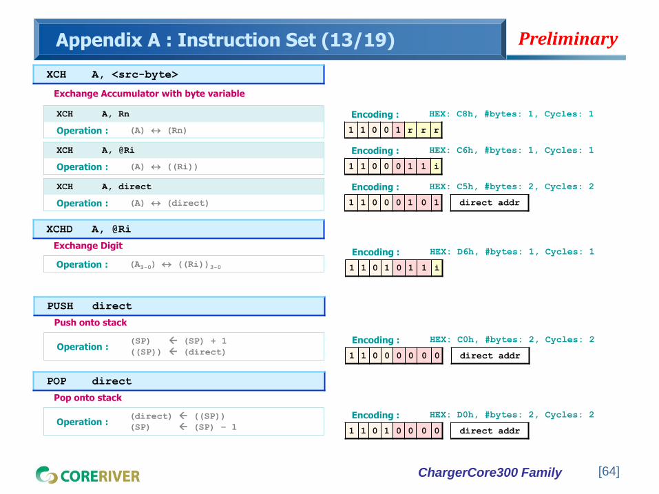
Appendix A : Instruction Set (13/19)
XCH A, Rn
Operation : (A) (Rn)
XCH A, @Ri
Operation : (A) ((Ri))
XCH A, direct
Operation : (A) (direct)
Encoding : HEX: C8h, #bytes: 1, Cycles: 1
1 1 0 0 1 r r r
Encoding : HEX: C6h, #bytes: 1, Cycles: 1
1 1 0 0 0 1 1 i
Encoding : HEX: C5h, #bytes: 2, Cycles: 2
1 1 0 0 0 1 0 1 direct addr
XCH A, <src-byte>
Exchange Accumulator with byte variable
PUSH direct
Operation : (SP) (SP) + 1
((SP)) (direct)
Push onto stack
Encoding : HEX: C0h, #bytes: 2, Cycles: 2
1 1 0 0 0 0 0 0 direct addr
POP direct
Operation : (direct) ((SP))
(SP) (SP) – 1
Pop onto stack
Encoding : HEX: D0h, #bytes: 2, Cycles: 2
1 1 0 1 0 0 0 0 direct addr
XCHD A, @Ri
Operation : (A3-0) ((Ri))3-0
Exchange Digit Encoding : HEX: D6h, #bytes: 1, Cycles: 1
1 1 0 1 0 1 1 i

ChargerCore300 Family
Preliminary
[65]
Appendix A : Instruction Set (14/19)
SETB <bit>
SETB C
Operation : (C) 1
Encoding : HEX: D3h, #bytes: 1, Cycles: 1
1 1 0 1 0 0 1 1
Set bit
SETB bit
Operation : (bit) 1
Encoding : HEX: D2h, #bytes: 2, Cycles: 2
1 1 0 1 0 0 1 0 bit addr
JC rel
Operation : (PC) (PC) + 2
If (C) = 1, then (PC) (PC) + rel
Jump if Carry is set
Encoding : HEX: 40h, #bytes: 2, Cycles: 3
0 1 0 0 0 0 0 0 relative addr
JNC rel
Operation : (PC) (PC) + 2
If (C) = 0, then (PC) (PC) + rel
Jump if Carry is not set
Encoding : HEX: 50h, #bytes: 2, Cycles: 3
0 1 0 1 0 0 0 0 relative addr
JB bit, rel
Operation : (PC) (PC) + 3
If (bit) = 1, then (PC) (PC)+rel
Jump if Bit is set
Encoding : HEX: 20h, #bytes: 3, Cycles: 4
0 0 1 0 0 0 0 0 bit addr relative addr
JNB bit, rel
Operation : (PC) (PC) + 3
If (bit) = 0, then (PC) (PC)+rel
Jump if Bit is not set
Encoding : HEX: 30h, #bytes: 3, Cycles: 4
0 0 1 1 0 0 0 0 bit addr relative addr

ChargerCore300 Family
Preliminary
[66]
Appendix A : Instruction Set (15/19)
JBC bit, rel
Operation :
(PC) (PC) + 3
If (bit) = 1,
then (bit) 0, (PC) (PC) + rel
Jump if Bit is set and Clear bit
Encoding : HEX: 10h, #bytes: 3, Cycles: 4
0 0 0 1 0 0 0 0 bit addr relative addr
ACALL addr11
Operation :
(PC) (PC) + 2
(SP) (SP) + 1
((SP)) (PC7-0)
(SP) (SP) + 1
((SP)) (PC15-8)
(PC10-0) page address
Absolute Subroutine Call
Encoding : HEX: 11h, #bytes: 2, Cycles: 3
a10 a9 a8 1 0 0 0 1 a7-0
LCALL addr16
Long Subroutine Call
Encoding : HEX: 12h, #bytes: 3, Cycles: 4
0 0 0 1 0 0 1 0 a15-8 a7-0
Operation :
(PC) (PC) + 3
(SP) (SP) + 1
((SP)) (PC7-0)
(SP) (SP) + 1
((SP)) (PC15-8)
(PC) addr15-0
ChargerCore300 Family
Preliminary
[67]
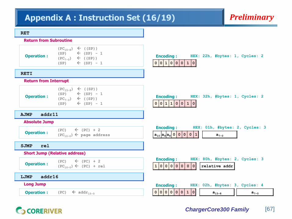
Appendix A : Instruction Set (16/19)
RET
Operation :
(PC15-8) ((SP))
(SP) (SP) - 1
(PC7-0) ((SP))
(SP) (SP) - 1
Return from Subroutine
Encoding : HEX: 22h, #bytes: 1, Cycles: 2
0 0 1 0 0 0 1 0
RETI
Operation :
(PC15-8) ((SP))
(SP) (SP) - 1
(PC7-0) ((SP))
(SP) (SP) - 1
Return from Interrupt
Encoding : HEX: 32h, #bytes: 1, Cycles: 2
0 0 1 1 0 0 1 0
AJMP addr11
Operation : (PC) (PC) + 2
(PC10-0) page address
Absolute Jump
Encoding : HEX: 01h, #bytes: 2, Cycles: 3
a10 a9 a8 0 0 0 0 1 a7-0
SJMP rel
Operation : (PC) (PC) + 2
(PC10-0) (PC) + rel
Short Jump (Relative address)
Encoding : HEX: 80h, #bytes: 2, Cycles: 3
1 0 0 0 0 0 0 0 relative addr
LJMP addr16
Operation : (PC) addr15-0
Long Jump Encoding : HEX: 02h, #bytes: 3, Cycles: 4
0 0 0 0 0 0 1 0 a15-8 a7-0
ChargerCore300 Family
Preliminary
[68]
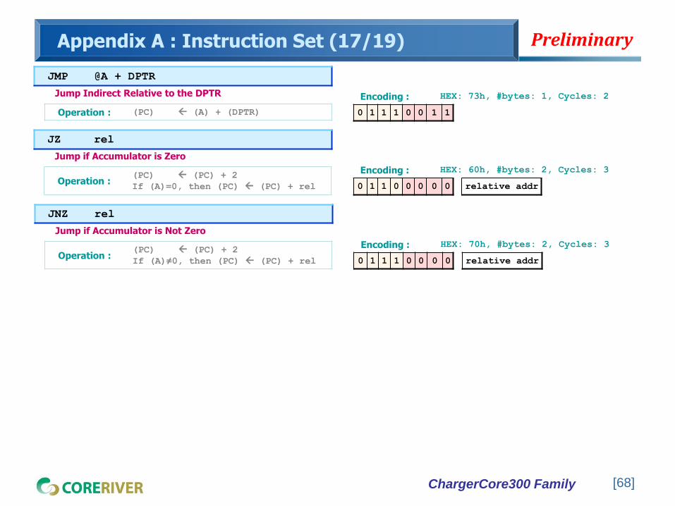
Appendix A : Instruction Set (17/19)
JMP @A + DPTR
Operation : (PC) (A) + (DPTR)
Jump Indirect Relative to the DPTR Encoding : HEX: 73h, #bytes: 1, Cycles: 2
0 1 1 1 0 0 1 1
JZ rel
Operation : (PC) (PC) + 2
If (A)=0, then (PC) (PC) + rel
Jump if Accumulator is Zero
Encoding : HEX: 60h, #bytes: 2, Cycles: 3
0 1 1 0 0 0 0 0 relative addr
JNZ rel
Operation : (PC) (PC) + 2
If (A)≠0, then (PC) (PC) + rel
Jump if Accumulator is Not Zero
Encoding : HEX: 70h, #bytes: 2, Cycles: 3
0 1 1 1 0 0 0 0 relative addr

ChargerCore300 Family
Preliminary
[69]
Appendix A : Instruction Set (18/19)
CJNE <dest-byte>, <src-byte>, rel
CJNE A, direct, rel
Operation :
(PC) (PC) + 3
If (A) ≠ (direct),
then (PC) (PC) + rel
If (A) < (direct), then (C) 1
Else (C) 0
Compare and Jump if Not Equal
Encoding : HEX: B5h, #bytes: 3, Cycles: 4
1 0 1 1 0 1 0 1 direct addr relative addr
CJNE A, #data, rel
Operation :
(PC) (PC) + 3
If (A) ≠ data,
then (PC) (PC) + rel
If (A) < data, then (C) 1
Else (C) 0
Encoding : HEX: B4h, #bytes: 3, Cycles: 4
1 0 1 1 0 1 0 0 immediate data relative addr
CJNE Rn, #data, rel
Operation :
(PC) (PC) + 3
If (Rn) ≠ data,
then (PC) (PC) + rel
If (Rn) < data, then (C) 1
Else (C) 0
Encoding : HEX: B8h, #bytes: 3, Cycles: 4
1 0 1 1 1 r r r immediate data relative addr
CJNE @Ri, #data, rel
Operation :
(PC) (PC) + 3
If ((Ri)) ≠ data,
then (PC) (PC) + rel
If ((Ri)) < data, then (C) 1
Else (C) 0
Encoding : HEX: B6h, #bytes: 3, Cycles: 4
1 0 1 1 0 1 1 i immediate data relative addr

ChargerCore300 Family
Preliminary
[70]
Appendix A : Instruction Set (19/19)
DJNZ <byte>, rel
DJNZ Rn, rel
Operation :
(PC) (PC) + 2
(Rn) (Rn) - 1
If (Rn)≠0, then (PC) (PC) + rel
Decrement and Jump if Not Zero
Encoding : HEX: D8h, #bytes: 2, Cycles: 3
1 1 0 1 1 r r r relative addr
DJNZ direct, rel
Operation :
(PC) (PC) + 3
(direct) (direct) - 1
If (direct)≠0,
then (PC) (PC) + rel
Encoding : HEX: D5h, #bytes: 3, Cycles: 4
1 1 0 1 0 1 0 1 direct addr relative addr
NOP
Operation : (PC) (PC) + 1
No Operation Encoding : HEX: 00h, #bytes: 1, Cycles: 1
0 0 0 0 0 0 0 0

ChargerCore300 Family
Preliminary
[71]
Appendix B : SFR Description [80h ~ 87h] (1/10)
P0 (80h) : Port 0 Register
- P0.6 P0.5 P0.4 P0.3 P0.2 P0.1 P0.0
R/W(1) R/W(1) R/W(1) R/W(1) R/W(1) R/W(1) R/W(1) R/W(1)
Port 0 Register
SP (81h) : Stack Pointer Register
SP.7 SP.6 SP.5 SP.4 SP.3 SP.2 SP.1 SP.0
R/W(0) R/W(0) R/W(0) R/W(0) R/W(0) R/W(1) R/W(1) R/W(1)
Indicate where stack will start.
Increment by PUSH and decrement by POP.
DPL (82h) : Data Pointer Low Register
DPL.7 DPL.6 DPL.5 DPL.4 DPL.3 DPL.2 DPL.1 DPL.0
R/W(0) R/W(0) R/W(0) R/W(0) R/W(0) R/W(0) R/W(0) R/W(0)
P0 (80h) : Port 0 Register
- P0.6 P0.5 P0.4 P0.3 P0.2 P0.1 P0.0
R/W(1) R/W(1) R/W(1) R/W(1) R/W(1) R/W(1) R/W(1) R/W(1)
[How to Read a SFR Descriptions]
Yellow Color : Bit Addressable
White Color : Byte Addressable
R : Unrestricted Read W : Unrestricted Write (n) : Reset Value
SFR Address
DPH (83h) : Data Pointer High Register
DPH.7 DPH.6 DPH.5 DPH.4 DPH.3 DPH.2 DPH.1 DPH.0
R/W(0) R/W(0) R/W(0) R/W(0) R/W(0) R/W(0) R/W(0) R/W(0)
PCON (87h) : Power Control Register
- - - POF GF1 GF0 PD IDL
R/W(1) R/W(0) R/W(0) R/W(0) R/W(0)
POF : Power off flag. When power-on, this bit will be set by H/W.
GF1, GF0 : General purpose flag bit. Initialized only by POR.
PD : Power-down (Stop) mode enable.
IDL : IDLE mode enable.

ChargerCore300 Family
Preliminary
[72]
Appendix B : SFR Description [88h ~ 8Fh] (2/10)
TCON (88h) : Timer/Counter 0/1 Control Register
TF1 TR1 TF0 TR0 IE1 IT1 IE0 IT0
R/W(0) R/W(0) R/W(0) R/W(0) R/W(0) R/W(0) R/W(0) R/W(0)
TF1 : Timer 1 overflow flag.
TR1 : Timer 1 run enable.
TF0 : Timer 0 overflow flag.
TR0 : Timer 0 run enable.
IE1 : External interrupt 1 flag. If IT1 = 0, cleared by S/W (software). If IT1 = 1, cleared automatically when go to routine.
IT1 : External interrupt 1 TYP select flag. Falling Edge Detect (IT1=1). Low Level Detect (IT1=0).
IE0 : External interrupt 0 flag. If IT0 = 0, cleared by S/W (software). If IT0 = 1, cleared automatically when go to routine.
IT0 : External interrupt 0 TYP select flag. Falling Edge Detect (IT0=1). Low Level Detect (IT0=0).
TMOD (89h) : Timer/Counter 0 Mode Control Register
- - - - GATE C/T M1 M0
R/W(0) R/W(0) R/W(0) R/W(0)
GATE[3] : Timer 0 gate control.
C/T[2] : Timer 0 Counter/Timer select. 0 = Timer by FOSC/12. (Default) 1 = Counter by T0 pin.
M1, M0 : Timer 0 mode selection. [0,0] : Mode0, 13-bit T/C [0,1] : Mode1, 16-bit T/C [1,0] : Mode2, 8-bit T/C with auto-reload [1,1] : Mode3, Two 8-bit T/C
TL0 (8Ah) : Timer/Counter 0 Low Byte Register
TL0.7 TL0.6 TL0.5 TL0.4 TL0.3 TL0.2 TL0.1 TL0.0
R/W(0) R/W(0) R/W(0) R/W(0) R/W(0) R/W(0) R/W(0) R/W(0)
TL1 (8Bh) : Timer/Counter 1 Low Byte Register
TL1.7 TL1.6 TL1.5 TL1.4 TL1.3 TL1.2 TL1.1 TL1.0
R/W(0) R/W(0) R/W(0) R/W(0) R/W(0) R/W(0) R/W(0) R/W(0)
TH0 (8Ch) : Timer/Counter 0 High Byte Register
TH0.7 TH0.6 TH0.5 TH0.4 TH0.3 TH0.2 TH0.1 TH0.0
R/W(0) R/W(0) R/W(0) R/W(0) R/W(0) R/W(0) R/W(0) R/W(0)
TH1 (8Dh) : Timer/Counter 1 High Byte Register
TH1.7 TH1.6 TH1.5 TH1.4 TH1.3 TH1.2 TH1.1 TH1.0
R/W(0) R/W(0) R/W(0) R/W(0) R/W(0) R/W(0) R/W(0) R/W(0)

ChargerCore300 Family
Preliminary
[73]
Appendix B : SFR Description [90h ~ 9Fh] (3/10)
P1 (90h) : Port 1 Register
- - - - - P1.2 P1.1 P1.0
R/W(1) R/W(1) R/W(1)
P1.0 : XTAL 1 alternative. (Default = XTAL1).
P1.1 : XTAL 2 alternative. (Default = XTAL2). Refer to ALTSEL & PMR SFR for I/O pins.
P1.2 : RESETB alternative. (Default = RESETB) Refer to ALTSEL for I/O Pins.
RINGCON (95h: Internal Oscillator Frequency Tuning
S7 S6 S5 S4 S3 S2 S1 S0
R/W(1) R/W(0) R/W(0) R/W(0) R/W(0) R/W(0) R/W(0) R/W(0)
OSCREF(97h) : Internal Oscillator Reference Tuning
- - - S4 S3 S2 S1 S0
R/W(1) R/W(0) R/W(1) R/W(1) R/W(1)
OSCBIAS (96h) : Internal Oscillator Bias Current Tuning
S7 S6 S5 S4 S3 S2 S1 S0
R/W(0) R/W(1) R/W(0) R/W(1) R/W(1) R/W(1) R/W(1) R/W(1)
EXIF (91h) : External Interrupt Flag Register
- XT/RG RGMD RGSL BGS
- R/W(0) R(1) R(1) R/W(1)
XT/RG : System clock selection. 0 = Internal Precision oscillator is selected as system clock. 1 = External clock is selected as system clock.
RGMD : RCLK mode. Now system clock is POSC or XTAL. Generally RGMD is the invert of XT/RG.
RGSL : RCLK select bit when power-down wake-up. If set, when wake-up from power-down in XTAL clock,
use RCLK as system clock during the first 65,536 cycles.
This bit is always 1.
BGS : Band-gap select. (Default = 1) If 0, Band-gap block (POR) will be off in power-down mode.
If 1, Band-gap block (POR) will run in power-down mode.
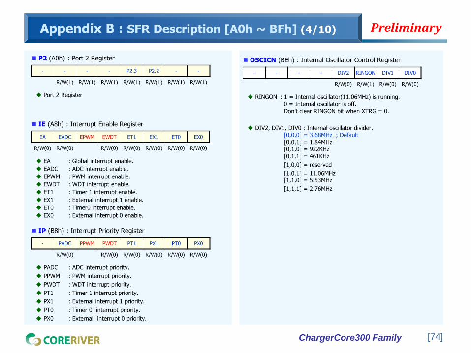
ChargerCore300 Family
Preliminary
[74]
Appendix B : SFR Description [A0h ~ BFh] (4/10)
P2 (A0h) : Port 2 Register
- - - - P2.3 P2.2 - -
R/W(1) R/W(1) R/W(1) R/W(1) R/W(1) R/W(1) R/W(1)
Port 2 Register
IE (A8h) : Interrupt Enable Register
EA EADC EPWM EWDT ET1 EX1 ET0 EX0
R/W(0) R/W(0) R/W(0) R/W(0) R/W(0) R/W(0) R/W(0)
EA : Global interrupt enable.
EADC : ADC interrupt enable.
EPWM : PWM interrupt enable.
EWDT : WDT interrupt enable.
ET1 : Timer 1 interrupt enable.
EX1 : External interrupt 1 enable.
ET0 : Timer0 interrupt enable.
EX0 : External interrupt 0 enable.
IP (B8h) : Interrupt Priority Register
- PADC PPWM PWDT PT1 PX1 PT0 PX0
R/W(0) R/W(0) R/W(0) R/W(0) R/W(0) R/W(0)
PADC : ADC interrupt priority.
PPWM : PWM interrupt priority.
PWDT : WDT interrupt priority.
PT1 : Timer 1 interrupt priority.
PX1 : External interrupt 1 priority.
PT0 : Timer 0 interrupt priority.
PX0 : External interrupt 0 priority.
OSCICN (BEh) : Internal Oscillator Control Register
- - - - DIV2 RINGON DIV1 DIV0
R/W(0) R/W(1) R/W(0) R/W(0)
RINGON : 1 = Internal oscillator(11.06MHz) is running. 0 = Internal oscillator is off. Don’t clear RINGON bit when XTRG = 0.
DIV2, DIV1, DIV0 : Internal oscillator divider. [0,0,0] = 3.68MHz ; Default [0,0,1] = 1.84MHz [0,1,0] = 922KHz [0,1,1] = 461KHz
[1,0,0] = reserved
[1,0,1] = 11.06MHz [1,1,0] = 5.53MHz
[1,1,1] = 2.76MHz

ChargerCore300 Family
Preliminary
[75]
Appendix B : SFR Description [C0h ~ CFh] (5/10)
PMR (C4h) : Power Management Control Register
- - - - XTOFF - - -
R/W(0)
XTOFF : Internal amplifier disable for external crystal oscillator.
1 = External crystal will be killed. 0 = External crystal will run (Default).
Don’t set XTOFF bit when XT/RG = 1.
STATUS (C5h) : Crystal Status Register
- - - XTUP - - - -
R(0)
XTUP : Crystal oscillator warm-up status.
It represents the crystal clock is stable (1) or not (0).
Cleared by H/W when Power-on reset and all kinds of reset.
Cleared by H/W when XTOFF bit is set.
Cleared by during Power-down wake-up when XT/RG = 1.
Set by H/W after XTAL stabilization time.
LVDCFG (C6h) : LVD Configuration Register
EPFR EPFI PFI CFG4 CFG3 CFG2 CFG1 CFG0
R/W(0) R/W(0) R/W(0) R/W(0) R/W(0) R(1) R/W(0) R/W(1)
EPFR : Power-fail reset enable.
EPFI : Power-fail interrupt enable.
PFI : Power-fail interrupt flag.
CFG[4:0] : LVD Voltage Selection
NOTE : This SFR is initialized only by power-on-reset. That is, it holds user’s setting for any other reset.
CFG[4:0] VLVD [V]
1 1111 5.0
1 1110 4.9
1 1101 4.8
1 1100 4.7
1 1011 4.6
1 1010 4.5
1 1001 4.4
1 1000 4.3
1 0111 4.2
1 0110 4.1
1 0101 4.0
1 0100 3.9
1 0011 3.8
1 0010 3.7
1 0001 3.6
1 0000 3.5
CFG[4:0] VLVD [V]
0 1111 3.4
0 1110 3.3
0 1101 3.2
0 1100 3.1
0 1011 3.0
0 1010 2.9
0 1001 2.8
0 1000 2.7
0 0111 2.6
0 0110 2.5
0 0101 2.4
0 0100 2.3
0 0011 2.2
0 0010 2.1
0 0001 2.0
0 0000 1.9

ChargerCore300 Family
Preliminary
[76]
Appendix B : SFR Description [D0h ~ D7h] (6/10)
PSW (D0h) : Program Status Word Register
CY AC F0 RS1 RS0 OV F1 P
R/W(0) R/W(0) R/W(0) R/W(0) R/W(0) R/W(0) R/W(0) R(0)
CY : Carry flag.
AC : Auxiliary carry flag.
F0 : User flag 0.
RS1, RS0 : Register bank select. [0,0] : Bank 0 [1,0] : Bank 2 [0,1] : Bank 1 [1,1] : Bank 3
OV : Overflow flag.
F1 : User flag 1.
P : Parity bit. Set/clear by H/W according to ACC odd parity.
P1TYPE (D5h) : Port 1 TYPE Control Register
P1TYPE.2 P1TYPE.1 P1TYPE.0
R/W(0) R/W(0) R/W(0)
0 = Push-pull Output (Default) / 1 = Open-drain output
P0TYPE (D4h) : Port 0 TYPE Control Register
- P0TYPE.6 P0TYPE.5 P0TYPE.4 P0TYPE.3 P0TYPE.2 P0TYPE.1 P0TYPE.0
R/W(0) R/W(0) R/W(0) R/W(0) R/W(0) R/W(0) R/W(0) R/W(0)
0 = Push-pull Output (Default) / 1 = Open-drain Output
P2TYPE (D6h) : Port 2 TYPE Control Register
- - - P2TYPE.3 P2TYPE.2 - -
R/W(0) R/W(0) R/W(0) R/W(0) R/W(0) R/W(0) R/W(0)
0 = Push-pull Output (Default) / 1 = Open-drain Output

ChargerCore300 Family
Preliminary
[77]
Appendix B : SFR Description [D8h ~ DFh] (7/10)
PWMCON (DCh) : PWM Control Register
PWM06 PS2_P0 PS1_P0 PS0_P0 - PWMF CLR_P0 RUN_P0
R/W(0) R/W(0) R/W(0) R/W(0) R(0) R/W(0) R/W(0) R/W(0)
PWM06 : PWM waveform output enable to P0.6.
PS2_P0, PS1_P0, PS0_P0 : Pre-scaled Clock Selection.
[0,0,0] = FOSC/1, [0,0,1] = FOSC/2, [0,1,0] = FOSC/4,
[0,1,1] = FOSC/8, [1,0,0] = FOSC/16, [1,0,1] = FOSC/32,
[1,1,0] = FOSC/64, [1,1,1] = FOSC/128
RL_P0 : PWM data update mode selector. RL_P0=0, update at 6-bit Counter Overflow. RL_P0=1, update at 8-bit Counter Overflow.
PWMF : PWM Interrupt Flag. Cleared by S/W
CLR_P0 : Counter reset enable. Cleared by H/W.
RUN_P0 : Counter start enable.
PWMD (DEh) : PWM Duty Data Register
PWMD.7 PWMD.6 PWMD.5 PWMD.4 PWMD.3 PWMD.2 PWMD.1 PWMD.0
R/W(0) R/W(0) R/W(0) R/W(0) R/W(0) R/W(0) R/W(0) R/W(0)
WDCON (D8h) : Watchdog Timer Control Register
WD1 WD0 WDM - WDIF WTRF EWT RWT
R/W(1) R/W(1) R/W(0) R(0) R/W(0) R/W(0) R/W(0) R/W(0)
WD1,WD0 : Watchdog timer mode select. [0,0] : 8 x 216 clocks (interrupt)
[0,1] : 16 x 216 clocks (interrupt)
[1,0] : 32 x 216 clocks (interrupt)
[1,1] : 64 x 216 clocks (interrupt)
WDM : Watchdog clock divide mode for Test (Do not set this bit in the application.)
WDIF : Watchdog Timer Interrupt Flag
WTRF : Watchdog timer Reset flag.
EWT : Watchdog timer Reset Enable.
RWT : Restart watchdog timer.
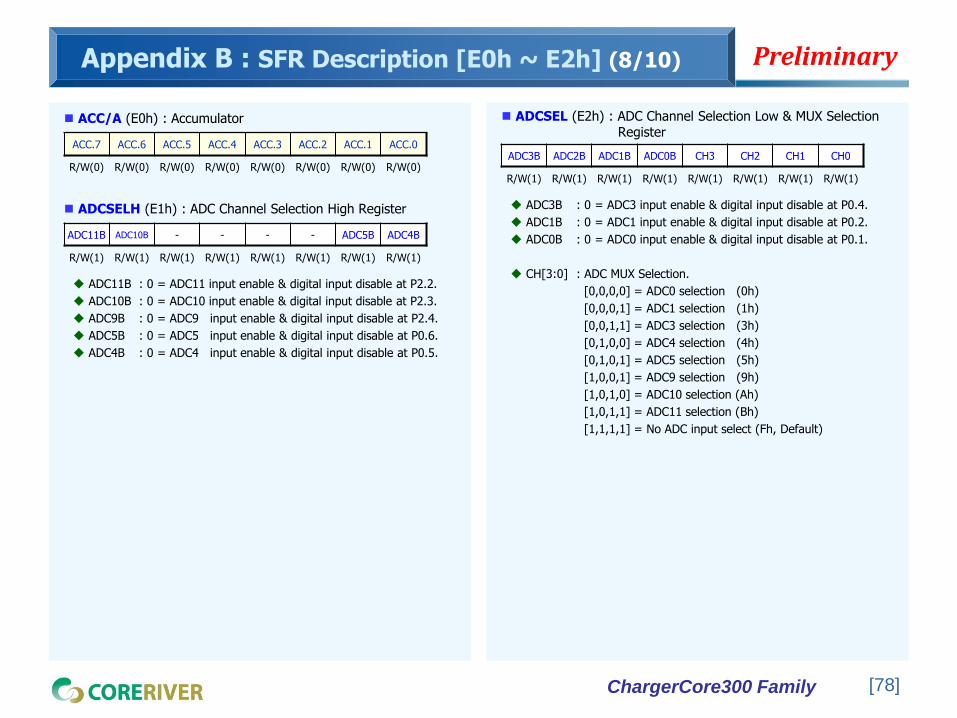
ChargerCore300 Family
Preliminary
[78]
Appendix B : SFR Description [E0h ~ E2h] (8/10)
ACC/A (E0h) : Accumulator
ACC.7 ACC.6 ACC.5 ACC.4 ACC.3 ACC.2 ACC.1 ACC.0
R/W(0) R/W(0) R/W(0) R/W(0) R/W(0) R/W(0) R/W(0) R/W(0)
ADCSELH (E1h) : ADC Channel Selection High Register
ADC11B ADC10B - - - - ADC5B ADC4B
R/W(1) R/W(1) R/W(1) R/W(1) R/W(1) R/W(1) R/W(1) R/W(1)
ADC11B : 0 = ADC11 input enable & digital input disable at P2.2.
ADC10B : 0 = ADC10 input enable & digital input disable at P2.3.
ADC9B : 0 = ADC9 input enable & digital input disable at P2.4.
ADC5B : 0 = ADC5 input enable & digital input disable at P0.6.
ADC4B : 0 = ADC4 input enable & digital input disable at P0.5.
ADCSEL (E2h) : ADC Channel Selection Low & MUX Selection Register
ADC3B ADC2B ADC1B ADC0B CH3 CH2 CH1 CH0
R/W(1) R/W(1) R/W(1) R/W(1) R/W(1) R/W(1) R/W(1) R/W(1)
ADC3B : 0 = ADC3 input enable & digital input disable at P0.4.
ADC1B : 0 = ADC1 input enable & digital input disable at P0.2.
ADC0B : 0 = ADC0 input enable & digital input disable at P0.1.
CH[3:0] : ADC MUX Selection.
[0,0,0,0] = ADC0 selection (0h)
[0,0,0,1] = ADC1 selection (1h)
[0,0,1,1] = ADC3 selection (3h)
[0,1,0,0] = ADC4 selection (4h)
[0,1,0,1] = ADC5 selection (5h)
[1,0,0,1] = ADC9 selection (9h)
[1,0,1,0] = ADC10 selection (Ah)
[1,0,1,1] = ADC11 selection (Bh)
[1,1,1,1] = No ADC input select (Fh, Default)

ChargerCore300 Family
Preliminary
[79]
Appendix B : SFR Description [E3h ~ EFh] (9/10)
ADCR (EEh) : ADC Result High Register : Value[9:2]
SAR9 SAR8 SAR7 SAR6 SAR5 SAR4 SAR3 SAR2
R/W(0) R/W(0) R/W(0) R/W(0) R/W(0) R/W(0) R/W(0) R/W(0)
ADCON (EFh) : ADC Control & ADC Result Low Register : Value[1:0]
AD_EN AD_REQ AD_END ADCF ADIV1 ADIV0 SAR1 SAR0
R/W(0) R/W(0) R(1) R/W(0) R/W(0) R/W(0) R/W(0) R/W(0)
AD_EN : ADC ready enable.
AD_REQ : ADC start.
Cleared by H/W when AD_END goes to 1 from 0.
AD_END : Current ADC status. 0 = ADC is running now.
ADCF : ADC interrupt flag. Must be cleared by S/W.
ADIV1, ADIV0 : ADC input clock select.
[0,0] = System clock (FSYS) / 2 (Default)
[0,1] = System clock (FSYS) / 4
[1,0] = System clock (FSYS) / 8
[1,1] = System clock (FSYS)
SAR1, SAR0 : Low bits of ADC result value.
P2SEL (E6h) : Port 2 Pull-up Control Register
- - - - P2SEL.3 P2SEL.2 - -
R/W(1) R/W(1) R/W(1) R/W(1) R/W(1) R/W(1) R/W(1)
0 = Pull-up resistor is ON
1 = Pull-up resistor is OFF (Default)
P0SEL (E4h) : Port 0 Pull-up Control Register
- P0SEL.6 P0SEL.5 P0SEL.4 P0SEL.3 P0SEL.2 P0SEL.1 P0SEL.0
R/W(1) R/W(1) R/W(1) R/W(1) R/W(1) R/W(1) R/W(0) R/W(0)
0 = Pull-up resistor is ON
1 = Pull-up resistor is OFF
P1SEL (E5h) : Port 1 Pull-up Control Register
- - - - - P1SEL.2 P1SEL.1 P1SEL.0
R/W(0) R/W(1) R/W(1)
0 = Pull-up resistor is ON
1 = Pull-up resistor is OFF
ALTSEL (E3h) : Alternative Function Control Register
XTAL_IOEN RST_IOEN CLO PWM00 TV0 - - -
R/W(0) R/W(0) R/W(0) R/W(0) R/W(0)
XTAL_IOEN : 1 = XTAL and XTAL2 is configured as I/O. Must be XTOFF (PMR.3) = 1 (Oscillator Amp. Off)
RST_IOEN : 1 = RESETB is configured as I/O.
CLO : 1 = System clock output to P2.6.
PWM00 : 1 = PWM waveform output enable to P0.0.
TVO : 1 = Timer 0 overflow clock to P0.0.

ChargerCore300 Family
Preliminary
[80]
Appendix B : SFR Description [F0h ~ FFh] (10/10)
B (F0h) : B Register
B.7 B.6 B.5 B.4 B.3 B.2 B.1 B.0
R/W(0) R/W(0) R/W(0) R/W(0) R/W(0) R/W(0) R/W(0) R/W(0)
P1DIR (F5h) : Port 1 Input/Output Control Register
- - - - - P1DIR.2 P1DIR.1 P1DIR.0
R/W(1) R/W(1) R/W(1)
1 = Input (Default) / 0 = Output
P2DIR (F6h) : Port 2 Input/Output Control Register
- - - - P2DIR.3 P2DIR.2 - -
R/W(1) R/W(1) R/W(1) R/W(1) R/W(1) R/W(1) R/W(1)
1 = Input (Default) / 0 = Output
P0DIR (F4h) : Port 0 Input/Output Control Register
- P0DIR.6 P0DIR.5 P0DIR.4 P0DIR.3 P0DIR.2 P0DIR.1 P0DIR.0
R/W(1) R/W(1) R/W(1) R/W(1) R/W(1) R/W(1) R/W(1) R/W(1)
1 = Input (Default) / 0 = Output
IAPWEN (FCh) : IAP Write/Erase Enable Register
WEN.7 WEN.6 WEN.5 WEN.4 WEN.3 WEN.2 WEN.1 WEN.0
R/W(0) R/W(0) R/W(0) R/W(0) R/W(0) R/W(0) R/W(0) R/W(0)
IAPCON (FDh) : IAP Control SFR
- - - - RGS1 RGS0 OPS1 OPS0
R/W(0) R/W(0) R/W(0) R/W(0)
RGS[1:0] : Select IAP region
00 : CODE (0x000 ~ 0x7FF)
01 : Reserved
10 : INFO (0x0 ~ 0xF)
11 : OTP (0x0 ~ 0xF)
OPS[1:0] : Select IAP function
00 : No operation
01 : Byte Read (IAPDAT ← F[DPTR])
10 : Byte Erase (F[DPTR] ← 0)
11 : Byte Write (F[DPTR] ← IAPDAT)
IAPDAT (FEh) : IAP read/write Data Register
DAT.7 DAT.6 DAT.5 DAT.4 DAT.3 DAT.2 DAT.1 DAT.0
R/W(0) R/W(0) R/W(0) R/W(0) R/W(0) R/W(0) R/W(0) R/W(0)

ChargerCore300 Family
Preliminary
[81] [81]
Appendix C : Update History
V1.0
First Release.


![midas DShop Auto-drafting Module for midas Gen 01 02admin.midasuser.com/UploadFiles2/84/Dshop_catalog.pdf · Auto-drafting Module for midas Gen [midas Gen Design Results] [midas DShop](https://static.fdocuments.net/doc/165x107/5ade06cd7f8b9a9a768db6e7/midas-dshop-auto-drafting-module-for-midas-gen-01-module-for-midas-gen-midas-gen.jpg)


![건설철강 주식회사 를 midas Gen / FEA 제안서 · 2018-04-05 · 5. midas FEA [ 사용자 인터페이스] [ 기하형상 모델링] midas Gen / Gen midas FEA [ 후처리](https://static.fdocuments.net/doc/165x107/5f4e6ff8b6f9633f2c3bc686/ee-oe-e-midas-gen-fea-oeoe-2018-04-05-5-midas-fea.jpg)