Microstructure of highly strained BiFeO thin films: Transmission ... · Microstructure of highly...
8
Microstructure of highly strained BiFeO 3 thin films: Transmission electron microscopy and electron-energy loss spectroscopy studies Young Heon Kim, 1,2,a) Akash Bhatnagar, 1 Eckhard Pippel, 1 Marin Alexe, 1,3 and Dietrich Hesse 1 1 Max Planck Institute of Microstructure Physics, Weinberg 2, D-06120 Halle, Germany 2 Korea Research Institute of Standards and Science (KRISS), Daejeon 305-340, South Korea 3 University of Warwick, Coventry CV4 7AL, West Midlands, United Kingdom (Received 28 October 2013; accepted 17 January 2014; published online 30 January 2014) Microstructure and electronic structure of highly strained bismuth ferrite (BiFeO 3 ) thin films grown on lanthanum aluminate substrates are studied using high-resolution transmission and scanning transmission electron microscopies and electron energy loss spectroscopy (EELS). Monoclinic and tetragonal phases were observed in films grown at different temperatures, and a mix of both phases was detected in a film grown at intermediate temperature. In this film, a smooth transition of the microstructure was found between the monoclinic and the tetragonal phases. A considerable increase in the c-axis parameters was observed in both phases compared with the rhombohedral bulk phase. The off-center displacement of iron (Fe) ions was increased in the monoclinic phase as compared with the tetragonal phase. EEL spectra show different electronic structures in the monoclinic and the tetragonal phases. These experimental observations are well consistent with the results of theoretical first-principle calculations performed. V C 2014 AIP Publishing LLC. [http://dx.doi.org/10.1063/1.4863778] I. INTRODUCTION Bismuth ferrite (BiFeO 3 , BFO) has been widely studied for its unique magnetoelectric properties at room temperature, such as antiferromagnetism coupled with ferroelectricity. It has been also shown to display various novel phenomena, e.g., an increased conductivity at specific ferroelectric domain walls, photovoltaic properties, and new structural phases in thin films. 1–7 Understanding microstructure and phase evolu- tion in multiferroic BFO thin films is an important issue, because interesting physical properties with practical applica- tions are related to the microstructure and phase identity. Although BFO is a rhombohedrally distorted multiferroic perovskite (space group R3c) in the bulk form, its structural stability is unclear in the form of thin films under strain. The misfit strain by lattice mismatch, one of the constraints in thin film growth, causes the distortion of the bulk structure and/or the stabilization of novel phases. A few research groups theo- retically suggested the existence of tetragonally-distorted BFO phases (space group P4mm) in strained thin films and several experimental researchers have recently reported the formation of highly elongated along the c-axis BFO phases on highly lattice-mismatched substrates, e.g., lanthanum alu- minate (LaAlO 3 , LAO), YAlO 3 , and NdAlO 3 . 8–12 In addition, the epitaxial strain is important for applications of BFO because it can improve the physical properties, increasing, e.g., spontaneous polarization and Curie temperature com- pared with the corresponding bulk materials. 13–17 However, the understanding of the phase evolution and atomic struc- tures of BFO thin films is still insufficient. There are a num- ber of fundamental questions to challenge, regarding the microstructure as well as dielectric and electronic properties, such as, e.g., What is the symmetry in distorted BFO thin-film phases? In this paper, we present a detailed investigation on the atomic and electronic structure of highly strained BFO thin films, based on a transmission electron microscopy (TEM) study. The transition between phases is considered to be a critical issue in achieving a highly polarized BFO phase. Morphology and microstructure of BFO thin films were studied by various transmission and scanning transmission electron microscopy techniques (in particular, with a probe Cs-corrector for atomic resolution in the latter case). We also show geometrical phase analysis (GPA) results adopted to evaluate the lattice parameters of the observed phases. Finally, we will briefly demonstrate the interplay between electronic properties and microstructure. The experimental observations are complemented by theoretical first-principle calculations. II. EXPERIMENTAL DETAILS Bismuth ferrite thin films were deposited using pulsed laser deposition (PLD) on LAO substrates. In this paper, we consider three BFO thin films grown at 600 C, 650 C, and 700 C, respectively. An excimer laser beam (wavelength k ¼ 248 nm, laser energy density 0.5 J/cm 2 , laser spot size 5 3 mm 2 ) was focused on a BiFeO 3 pressed powder target; the distance between the target and the (001) LaAlO 3 substrate was 5.0 cm. Film thickness amounted to about 20 nm. The base pressure of the vacuum chamber, P b , was 2–6 10 6 mbar, and the partial oxygen pressure during deposition, P O2 , was 2–6 10 5 mbar. After the deposition, the thin films were cooled to room temper- ature under oxygen pressure 175 6 25 mbar. The crystallographic phase and orientation of the BiFeO 3 thin films were determined by X-ray diffraction (XRD) with a a) Author to whom correspondence should be addressed. Electronic mail: [email protected] 0021-8979/2014/115(4)/043526/8/$30.00 V C 2014 AIP Publishing LLC 115, 043526-1 JOURNAL OF APPLIED PHYSICS 115, 043526 (2014)
Transcript of Microstructure of highly strained BiFeO thin films: Transmission ... · Microstructure of highly...
Microstructure of highly strained BiFeO3 thin films: Transmission electronmicroscopy and electron-energy loss spectroscopy studies
Young Heon Kim,1,2,a) Akash Bhatnagar,1 Eckhard Pippel,1 Marin Alexe,1,3
and Dietrich Hesse1
1Max Planck Institute of Microstructure Physics, Weinberg 2, D-06120 Halle, Germany2Korea Research Institute of Standards and Science (KRISS), Daejeon 305-340, South Korea3University of Warwick, Coventry CV4 7AL, West Midlands, United Kingdom
(Received 28 October 2013; accepted 17 January 2014; published online 30 January 2014)
Microstructure and electronic structure of highly strained bismuth ferrite (BiFeO3) thin films grown
on lanthanum aluminate substrates are studied using high-resolution transmission and scanning
transmission electron microscopies and electron energy loss spectroscopy (EELS). Monoclinic and
tetragonal phases were observed in films grown at different temperatures, and a mix of both phases
was detected in a film grown at intermediate temperature. In this film, a smooth transition of the
microstructure was found between the monoclinic and the tetragonal phases. A considerable
increase in the c-axis parameters was observed in both phases compared with the rhombohedral
bulk phase. The off-center displacement of iron (Fe) ions was increased in the monoclinic phase as
compared with the tetragonal phase. EEL spectra show different electronic structures in the
monoclinic and the tetragonal phases. These experimental observations are well consistent with the
results of theoretical first-principle calculations performed. VC 2014 AIP Publishing LLC.
[http://dx.doi.org/10.1063/1.4863778]
I. INTRODUCTION
Bismuth ferrite (BiFeO3, BFO) has been widely studied
for its unique magnetoelectric properties at room temperature,
such as antiferromagnetism coupled with ferroelectricity. It
has been also shown to display various novel phenomena,
e.g., an increased conductivity at specific ferroelectric domain
walls, photovoltaic properties, and new structural phases in
thin films.1–7 Understanding microstructure and phase evolu-
tion in multiferroic BFO thin films is an important issue,
because interesting physical properties with practical applica-
tions are related to the microstructure and phase identity.
Although BFO is a rhombohedrally distorted multiferroic
perovskite (space group R3c) in the bulk form, its structural
stability is unclear in the form of thin films under strain. The
misfit strain by lattice mismatch, one of the constraints in thin
film growth, causes the distortion of the bulk structure and/or
the stabilization of novel phases. A few research groups theo-
retically suggested the existence of tetragonally-distorted
BFO phases (space group P4mm) in strained thin films and
several experimental researchers have recently reported the
formation of highly elongated along the c-axis BFO phases
on highly lattice-mismatched substrates, e.g., lanthanum alu-
minate (LaAlO3, LAO), YAlO3, and NdAlO3.8–12 In addition,
the epitaxial strain is important for applications of BFO
because it can improve the physical properties, increasing,
e.g., spontaneous polarization and Curie temperature com-
pared with the corresponding bulk materials.13–17 However,
the understanding of the phase evolution and atomic struc-
tures of BFO thin films is still insufficient. There are a num-
ber of fundamental questions to challenge, regarding the
microstructure as well as dielectric and electronic properties,
such as, e.g., What is the symmetry in distorted BFO
thin-film phases?
In this paper, we present a detailed investigation on the
atomic and electronic structure of highly strained BFO thin
films, based on a transmission electron microscopy (TEM)
study. The transition between phases is considered to be a
critical issue in achieving a highly polarized BFO phase.
Morphology and microstructure of BFO thin films were
studied by various transmission and scanning transmission
electron microscopy techniques (in particular, with a probe
Cs-corrector for atomic resolution in the latter case). We also
show geometrical phase analysis (GPA) results adopted to
evaluate the lattice parameters of the observed phases. Finally,
we will briefly demonstrate the interplay between electronic
properties and microstructure. The experimental observations
are complemented by theoretical first-principle calculations.
II. EXPERIMENTAL DETAILS
Bismuth ferrite thin films were deposited using pulsed laser
deposition (PLD) on LAO substrates. In this paper, we consider
three BFO thin films grown at 600 �C, 650 �C, and 700 �C,
respectively. An excimer laser beam (wavelength k¼ 248 nm,
laser energy density 0.5 J/cm2, laser spot size 5� 3 mm2) was
focused on a BiFeO3 pressed powder target; the distance
between the target and the (001) LaAlO3 substrate was 5.0 cm.
Film thickness amounted to about 20 nm. The base pressure of
the vacuum chamber, Pb, was 2–6� 10�6 mbar, and the partial
oxygen pressure during deposition, PO2, was 2–6� 10�5 mbar.
After the deposition, the thin films were cooled to room temper-
ature under oxygen pressure 175 6 25 mbar.
The crystallographic phase and orientation of the BiFeO3
thin films were determined by X-ray diffraction (XRD) with a
a)Author to whom correspondence should be addressed. Electronic mail:
0021-8979/2014/115(4)/043526/8/$30.00 VC 2014 AIP Publishing LLC115, 043526-1
JOURNAL OF APPLIED PHYSICS 115, 043526 (2014)
Philips X’Pert MRD diffractometer. Reciprocal space maps
(RSMs) around the (103) reflection were taken to study the
crystalline properties and lattice parameters. TEM was
employed to study the details of the microstructure of the
films. Specimens for TEM were prepared by a gallium
focused ion beam (FIB). Bright-field (BF) TEM images and
selected-area electron diffraction (SAED) patterns were taken
using a Philips CM20T electron microscope at 200 kV.
High-resolution (HR) TEM and STEM micrographs were
obtained on a Jeol 4010 microscope having a point resolution
of 1.6 A at 400 kV and a FEI Cs-probe corrected TITAN
80–300 microscope having a point resolution of 0.80 A,
respectively. Electron-energy loss spectroscopy experiments
were carried out in the FEI TITAN 80–300 microscope, using
a GIF tridium system from Gatan, Inc.
The atomic structure of the experimentally observed
phases was simulated by using density functional theory
(DFT) calculations as implented in the Vienna ab initio sim-
ulation package (VASP). The generalized gradient approxi-
mation (GGA) (with the Perdew-Burke-Ernzerhoof (PBE)
exchange model) was used for the simulation. A “Hubbard-
U” scheme, with parameters U¼ 4 eV, and J¼ 1 eV, was
used for a better treatment of the 3d electrons of iron. A ki-
netic energy cutoff of 600 eV and the 2� 2� 2 k-point mesh
in the Brilliouin zone (BZ) corresponding to the supercell
with 40 atoms (bismuth:8, iron:8, and oxygen:24) were used.
The calculation conditions were checked from converged
results. The supercell was constructed by doubling the perov-
skite structure with a five-atom cell along the three axis
directions of the pseudocubic structure, denoted by x, y, and
z. The structure is compatible with the G-type antiferromag-
netic spin arrangement known to be most relevant for BFO.
III. RESULTS AND DISCUSSION
A. Microstructure
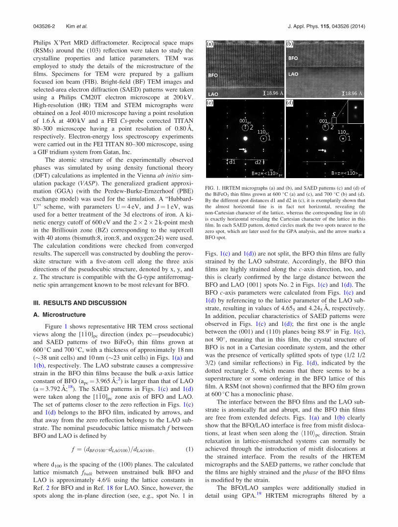
Figure 1 shows representative HR TEM cross sectional
views along the [1�10]pc direction (index pc—pseudocubic)
and SAED patterns of two BiFeO3 thin films grown at
600 �C and 700 �C, with a thickness of approximately 18 nm
(�38 unit cells) and 10 nm (�23 unit cells) in Figs. 1(a) and
1(b), respectively. The LAO substrate causes a compressive
strain in the BFO thin films because the bulk a-axis lattice
constant of BFO (apc¼ 3.965 A;2) is larger than that of LAO
(a¼ 3.792 A;18). The SAED patterns in Figs. 1(c) and 1(d)
were taken along the [1�10]pc zone axis of BFO and LAO.
The set of patterns closer to the zero reflection in Figs. 1(c)
and 1(d) belongs to the BFO film, indicated by arrows, and
that away from the zero reflection belongs to the LAO sub-
strate. The nominal pseudocubic lattice mismatch f between
BFO and LAO is defined by
f ¼ ðdBFO100–dLAO100Þ=dLAO100; (1)
where d100 is the spacing of the (100) planes. The calculated
lattice mismatch fbulk between unstrained bulk BFO and
LAO is approximately 4.6% using the lattice constants in
Ref. 2 for BFO and in Ref. 18 for LAO. Since, however, the
spots along the in-plane direction (see, e.g., spot No. 1 in
Figs. 1(c) and 1(d)) are not split, the BFO thin films are fully
strained by the LAO substrate. Accordingly, the BFO thin
films are highly strained along the c-axis direction, too, and
this is clearly confirmed by the large distance between the
BFO and LAO {001} spots No. 2 in Figs. 1(c) and 1(d). The
BFO c-axis parameters were calculated from Figs. 1(c) and
1(d) by referencing to the lattice parameter of the LAO sub-
strate, resulting in values of 4.655 and 4.245 A, respectively.
In addition, peculiar characteristics of SAED patterns were
observed in Figs. 1(c) and 1(d); the first one is the angle
between the (001) and (110) planes being 88.9� in Fig. 1(c),
not 90�, meaning that in this film, the crystal structure of
BFO is not in a Cartesian coordinate system, and the other
was the presence of vertically splitted spots of type (1/2 1/2
3/2) (and similar reflections) in Fig. 1(d), indicated by the
dotted rectangle S, which means that there seems to be a
superstructure or some ordering in the BFO lattice of this
film. A RSM (not shown) confirmed that the BFO film grown
at 600 �C has a monoclinic phase.
The interface between the BFO films and the LAO sub-
strate is atomically flat and abrupt, and the BFO thin films
are free from extended defects. Figs. 1(a) and 1(b) clearly
show that the BFO/LAO interface is free from misfit disloca-
tions, at least when seen along the h110ipc direction. Strain
relaxation in lattice-mismatched systems can normally be
achieved through the introduction of misfit dislocations at
the strained interface. From the results of the HRTEM
micrographs and the SAED patterns, we rather conclude that
the films are highly strained and the phase of the BFO films
is modified by the strain.
The BFO/LAO samples were additionally studied in
detail using GPA.19 HRTEM micrographs filtered by a
FIG. 1. HRTEM micrographs (a) and (b), and SAED patterns (c) and (d) of
the BiFeO3 thin films grown at 600 �C (a) and (c), and 700 �C (b) and (d).
By the different spot distances d1 and d2 in (c), it is exemplarily shown that
the almost horizontal line is in fact not horizontal, revealing the
non-Cartesian character of the lattice, whereas the corresponding line in (d)
is exactly horizontal revealing the Cartesian character of the lattice in this
film. In each SAED pattern, dotted circles mark the two spots nearest to the
zero spot, which are later used for the GPA analysis, and the arrow marks a
BFO spot.
043526-2 Kim et al. J. Appl. Phys. 115, 043526 (2014)
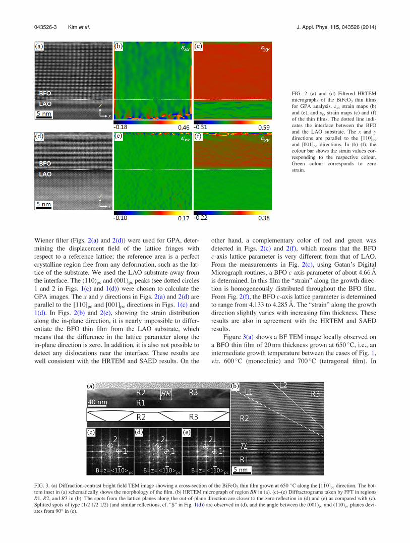
Wiener filter (Figs. 2(a) and 2(d)) were used for GPA, deter-
mining the displacement field of the lattice fringes with
respect to a reference lattice; the reference area is a perfect
crystalline region free from any deformation, such as the lat-
tice of the substrate. We used the LAO substrate away from
the interface. The (110)pc and (001)pc peaks (see dotted circles
1 and 2 in Figs. 1(c) and 1(d)) were chosen to calculate the
GPA images. The x and y directions in Figs. 2(a) and 2(d) are
parallel to the [110]pc and [001]pc directions in Figs. 1(c) and
1(d). In Figs. 2(b) and 2(e), showing the strain distribution
along the in-plane direction, it is nearly impossible to differ-
entiate the BFO thin film from the LAO substrate, which
means that the difference in the lattice parameter along the
in-plane direction is zero. In addition, it is also not possible to
detect any dislocations near the interface. These results are
well consistent with the HRTEM and SAED results. On the
other hand, a complementary color of red and green was
detected in Figs. 2(c) and 2(f), which means that the BFO
c-axis lattice parameter is very different from that of LAO.
From the measurements in Fig. 2(c), using Gatan’s Digital
Micrograph routines, a BFO c-axis parameter of about 4.66 A
is determined. In this film the “strain” along the growth direc-
tion is homogeneously distributed throughout the BFO film.
From Fig. 2(f), the BFO c-axis lattice parameter is determined
to range from 4.133 to 4.285 A. The “strain” along the growth
direction slightly varies with increasing film thickness. These
results are also in agreement with the HRTEM and SAED
results.
Figure 3(a) shows a BF TEM image locally observed on
a BFO thin film of 20 nm thickness grown at 650 �C, i.e., an
intermediate growth temperature between the cases of Fig. 1,
viz. 600 �C (monoclinic) and 700 �C (tetragonal film). In
FIG. 2. (a) and (d) Filtered HRTEM
micrographs of the BiFeO3 thin films
for GPA analysis. exx strain maps (b)
and (e), and eyy strain maps (c) and (f)
of the thin films. The dotted line indi-
cates the interface between the BFO
and the LAO substrate. The x and ydirections are parallel to the [110]pc
and [001]pc directions. In (b)–(f), the
colour bar shows the strain values cor-
responding to the respective colour.
Green colour corresponds to zero
strain.
FIG. 3. (a) Diffraction-contrast bright field TEM image showing a cross-section of the BiFeO3 thin film grown at 650 �C along the [1�10]pc direction. The bot-
tom inset in (a) schematically shows the morphology of the film. (b) HRTEM micrograph of region BR in (a). (c)–(e) Diffractrograms taken by FFT in regions
R1, R2, and R3 in (b). The spots from the lattice planes along the out-of-plane direction are closer to the zero reflection in (d) and (e) as compared with (c).
Splitted spots of type (1/2 1/2 1/2) (and similar reflections, cf. “S” in Fig. 1(d)) are observed in (d), and the angle between the (001)pc and (110)pc planes devi-
ates from 90� in (e).
043526-3 Kim et al. J. Appl. Phys. 115, 043526 (2014)
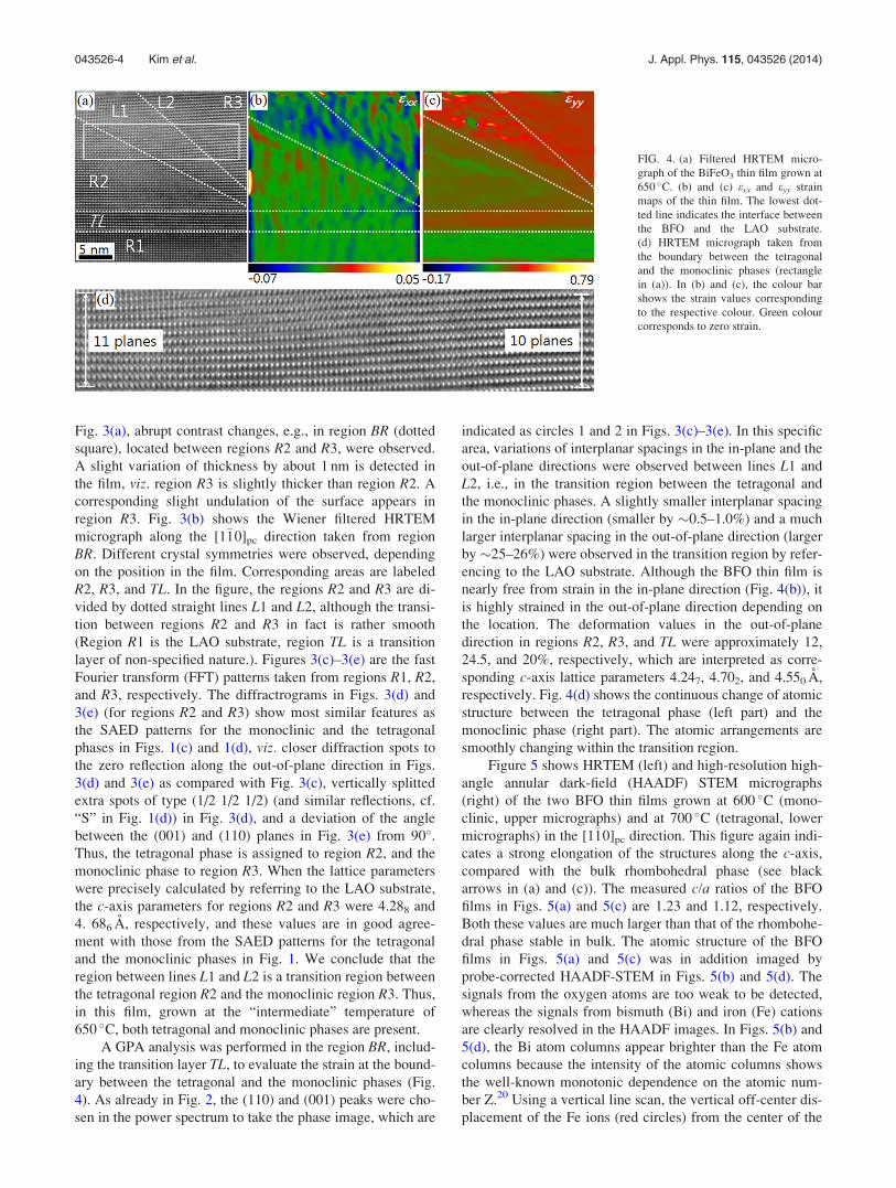
Fig. 3(a), abrupt contrast changes, e.g., in region BR (dotted
square), located between regions R2 and R3, were observed.
A slight variation of thickness by about 1 nm is detected in
the film, viz. region R3 is slightly thicker than region R2. A
corresponding slight undulation of the surface appears in
region R3. Fig. 3(b) shows the Wiener filtered HRTEM
micrograph along the [1�10]pc direction taken from region
BR. Different crystal symmetries were observed, depending
on the position in the film. Corresponding areas are labeled
R2, R3, and TL. In the figure, the regions R2 and R3 are di-
vided by dotted straight lines L1 and L2, although the transi-
tion between regions R2 and R3 in fact is rather smooth
(Region R1 is the LAO substrate, region TL is a transition
layer of non-specified nature.). Figures 3(c)–3(e) are the fast
Fourier transform (FFT) patterns taken from regions R1, R2,
and R3, respectively. The diffractrograms in Figs. 3(d) and
3(e) (for regions R2 and R3) show most similar features as
the SAED patterns for the monoclinic and the tetragonal
phases in Figs. 1(c) and 1(d), viz. closer diffraction spots to
the zero reflection along the out-of-plane direction in Figs.
3(d) and 3(e) as compared with Fig. 3(c), vertically splitted
extra spots of type (1/2 1/2 1/2) (and similar reflections, cf.
“S” in Fig. 1(d)) in Fig. 3(d), and a deviation of the angle
between the (001) and (110) planes in Fig. 3(e) from 90�.Thus, the tetragonal phase is assigned to region R2, and the
monoclinic phase to region R3. When the lattice parameters
were precisely calculated by referring to the LAO substrate,
the c-axis parameters for regions R2 and R3 were 4.288 and
4. 686 A, respectively, and these values are in good agree-
ment with those from the SAED patterns for the tetragonal
and the monoclinic phases in Fig. 1. We conclude that the
region between lines L1 and L2 is a transition region between
the tetragonal region R2 and the monoclinic region R3. Thus,
in this film, grown at the “intermediate” temperature of
650 �C, both tetragonal and monoclinic phases are present.
A GPA analysis was performed in the region BR, includ-
ing the transition layer TL, to evaluate the strain at the bound-
ary between the tetragonal and the monoclinic phases (Fig.
4). As already in Fig. 2, the (110) and (001) peaks were cho-
sen in the power spectrum to take the phase image, which are
indicated as circles 1 and 2 in Figs. 3(c)–3(e). In this specific
area, variations of interplanar spacings in the in-plane and the
out-of-plane directions were observed between lines L1 and
L2, i.e., in the transition region between the tetragonal and
the monoclinic phases. A slightly smaller interplanar spacing
in the in-plane direction (smaller by �0.5–1.0%) and a much
larger interplanar spacing in the out-of-plane direction (larger
by �25–26%) were observed in the transition region by refer-
encing to the LAO substrate. Although the BFO thin film is
nearly free from strain in the in-plane direction (Fig. 4(b)), it
is highly strained in the out-of-plane direction depending on
the location. The deformation values in the out-of-plane
direction in regions R2, R3, and TL were approximately 12,
24.5, and 20%, respectively, which are interpreted as corre-
sponding c-axis lattice parameters 4.247, 4.702, and 4.550 A,
respectively. Fig. 4(d) shows the continuous change of atomic
structure between the tetragonal phase (left part) and the
monoclinic phase (right part). The atomic arrangements are
smoothly changing within the transition region.
Figure 5 shows HRTEM (left) and high-resolution high-
angle annular dark-field (HAADF) STEM micrographs
(right) of the two BFO thin films grown at 600 �C (mono-
clinic, upper micrographs) and at 700 �C (tetragonal, lower
micrographs) in the [1�10]pc direction. This figure again indi-
cates a strong elongation of the structures along the c-axis,
compared with the bulk rhombohedral phase (see black
arrows in (a) and (c)). The measured c/a ratios of the BFO
films in Figs. 5(a) and 5(c) are 1.23 and 1.12, respectively.
Both these values are much larger than that of the rhombohe-
dral phase stable in bulk. The atomic structure of the BFO
films in Figs. 5(a) and 5(c) was in addition imaged by
probe-corrected HAADF-STEM in Figs. 5(b) and 5(d). The
signals from the oxygen atoms are too weak to be detected,
whereas the signals from bismuth (Bi) and iron (Fe) cations
are clearly resolved in the HAADF images. In Figs. 5(b) and
5(d), the Bi atom columns appear brighter than the Fe atom
columns because the intensity of the atomic columns shows
the well-known monotonic dependence on the atomic num-
ber Z.20 Using a vertical line scan, the vertical off-center dis-
placement of the Fe ions (red circles) from the center of the
FIG. 4. (a) Filtered HRTEM micro-
graph of the BiFeO3 thin film grown at
650 �C. (b) and (c) exx and eyy strain
maps of the thin film. The lowest dot-
ted line indicates the interface between
the BFO and the LAO substrate.
(d) HRTEM micrograph taken from
the boundary between the tetragonal
and the monoclinic phases (rectangle
in (a)). In (b) and (c), the colour bar
shows the strain values corresponding
to the respective colour. Green colour
corresponds to zero strain.
043526-4 Kim et al. J. Appl. Phys. 115, 043526 (2014)
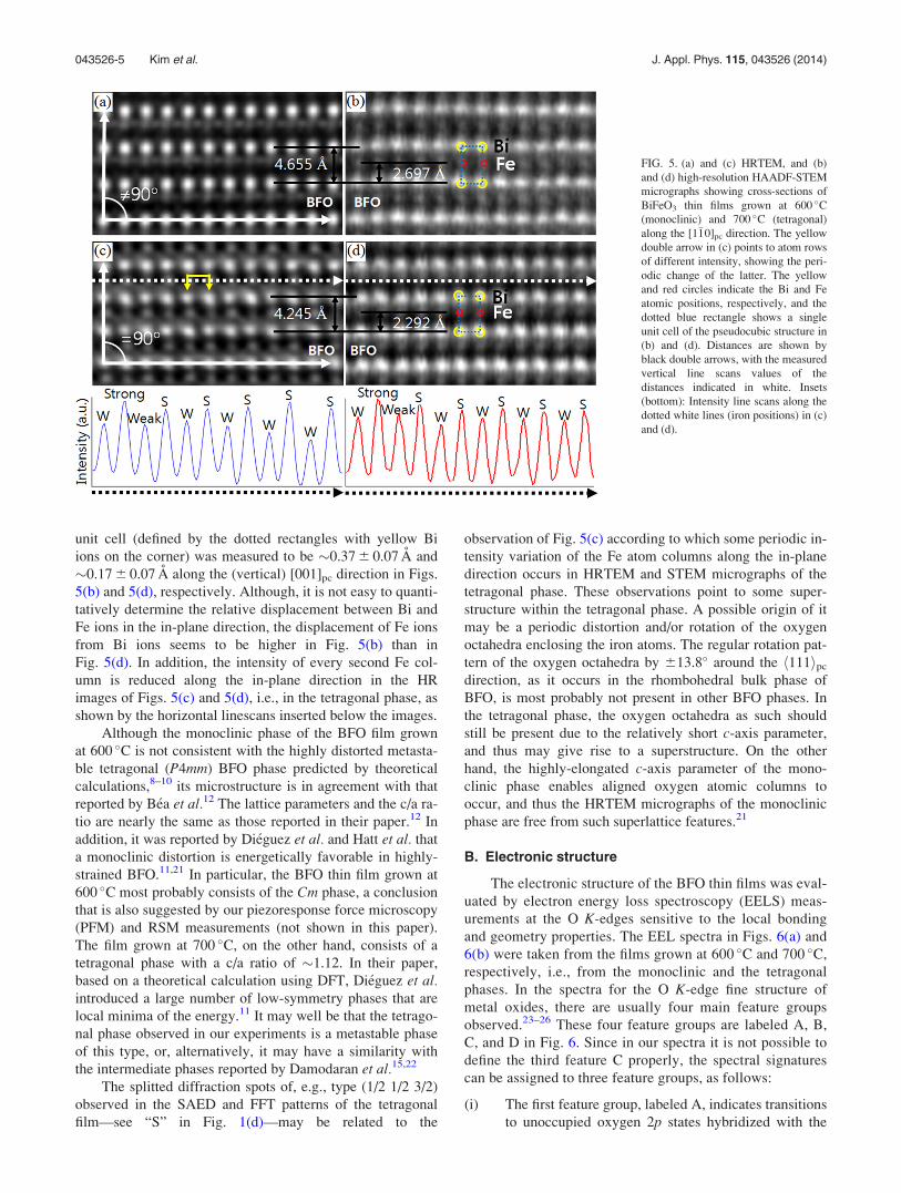
unit cell (defined by the dotted rectangles with yellow Bi
ions on the corner) was measured to be �0.37 6 0.07 A and
�0.17 6 0.07 A along the (vertical) [001]pc direction in Figs.
5(b) and 5(d), respectively. Although, it is not easy to quanti-
tatively determine the relative displacement between Bi and
Fe ions in the in-plane direction, the displacement of Fe ions
from Bi ions seems to be higher in Fig. 5(b) than in
Fig. 5(d). In addition, the intensity of every second Fe col-
umn is reduced along the in-plane direction in the HR
images of Figs. 5(c) and 5(d), i.e., in the tetragonal phase, as
shown by the horizontal linescans inserted below the images.
Although the monoclinic phase of the BFO film grown
at 600 �C is not consistent with the highly distorted metasta-
ble tetragonal (P4mm) BFO phase predicted by theoretical
calculations,8–10 its microstructure is in agreement with that
reported by B�ea et al.12 The lattice parameters and the c/a ra-
tio are nearly the same as those reported in their paper.12 In
addition, it was reported by Di�eguez et al. and Hatt et al. that
a monoclinic distortion is energetically favorable in highly-
strained BFO.11,21 In particular, the BFO thin film grown at
600 �C most probably consists of the Cm phase, a conclusion
that is also suggested by our piezoresponse force microscopy
(PFM) and RSM measurements (not shown in this paper).
The film grown at 700 �C, on the other hand, consists of a
tetragonal phase with a c/a ratio of �1.12. In their paper,
based on a theoretical calculation using DFT, Di�eguez et al.introduced a large number of low-symmetry phases that are
local minima of the energy.11 It may well be that the tetrago-
nal phase observed in our experiments is a metastable phase
of this type, or, alternatively, it may have a similarity with
the intermediate phases reported by Damodaran et al.15,22
The splitted diffraction spots of, e.g., type (1/2 1/2 3/2)
observed in the SAED and FFT patterns of the tetragonal
film—see “S” in Fig. 1(d)—may be related to the
observation of Fig. 5(c) according to which some periodic in-
tensity variation of the Fe atom columns along the in-plane
direction occurs in HRTEM and STEM micrographs of the
tetragonal phase. These observations point to some super-
structure within the tetragonal phase. A possible origin of it
may be a periodic distortion and/or rotation of the oxygen
octahedra enclosing the iron atoms. The regular rotation pat-
tern of the oxygen octahedra by 613.8� around the h111ipc
direction, as it occurs in the rhombohedral bulk phase of
BFO, is most probably not present in other BFO phases. In
the tetragonal phase, the oxygen octahedra as such should
still be present due to the relatively short c-axis parameter,
and thus may give rise to a superstructure. On the other
hand, the highly-elongated c-axis parameter of the mono-
clinic phase enables aligned oxygen atomic columns to
occur, and thus the HRTEM micrographs of the monoclinic
phase are free from such superlattice features.21
B. Electronic structure
The electronic structure of the BFO thin films was eval-
uated by electron energy loss spectroscopy (EELS) meas-
urements at the O K-edges sensitive to the local bonding
and geometry properties. The EEL spectra in Figs. 6(a) and
6(b) were taken from the films grown at 600 �C and 700 �C,
respectively, i.e., from the monoclinic and the tetragonal
phases. In the spectra for the O K-edge fine structure of
metal oxides, there are usually four main feature groups
observed.23–26 These four feature groups are labeled A, B,
C, and D in Fig. 6. Since in our spectra it is not possible to
define the third feature C properly, the spectral signatures
can be assigned to three feature groups, as follows:
(i) The first feature group, labeled A, indicates transitions
to unoccupied oxygen 2p states hybridized with the
FIG. 5. (a) and (c) HRTEM, and (b)
and (d) high-resolution HAADF-STEM
micrographs showing cross-sections of
BiFeO3 thin films grown at 600 �C(monoclinic) and 700 �C (tetragonal)
along the [1�10]pc direction. The yellow
double arrow in (c) points to atom rows
of different intensity, showing the peri-
odic change of the latter. The yellow
and red circles indicate the Bi and Fe
atomic positions, respectively, and the
dotted blue rectangle shows a single
unit cell of the pseudocubic structure in
(b) and (d). Distances are shown by
black double arrows, with the measured
vertical line scans values of the
distances indicated in white. Insets
(bottom): Intensity line scans along the
dotted white lines (iron positions) in (c)
and (d).
043526-5 Kim et al. J. Appl. Phys. 115, 043526 (2014)
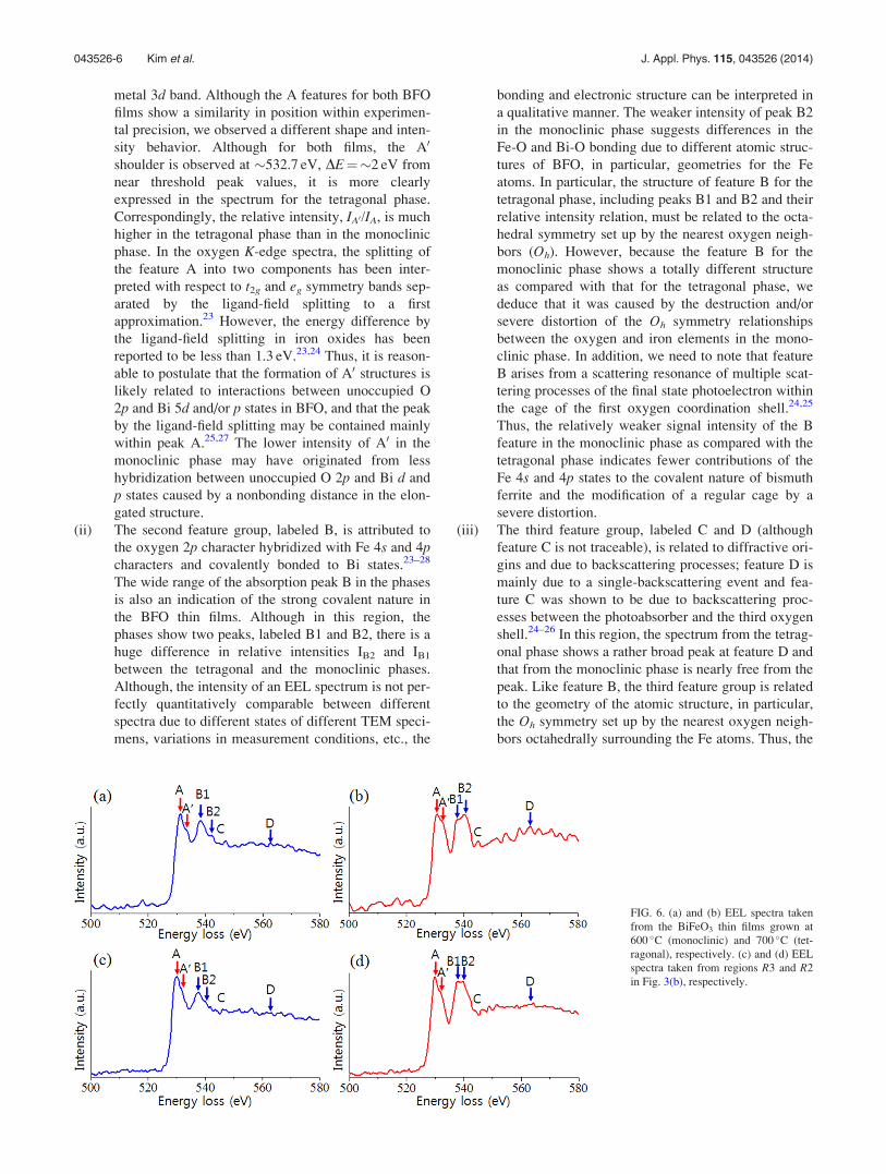
metal 3d band. Although the A features for both BFO
films show a similarity in position within experimen-
tal precision, we observed a different shape and inten-
sity behavior. Although for both films, the A0
shoulder is observed at �532.7 eV, DE¼�2 eV from
near threshold peak values, it is more clearly
expressed in the spectrum for the tetragonal phase.
Correspondingly, the relative intensity, IA0/IA, is much
higher in the tetragonal phase than in the monoclinic
phase. In the oxygen K-edge spectra, the splitting of
the feature A into two components has been inter-
preted with respect to t2g and eg symmetry bands sep-
arated by the ligand-field splitting to a first
approximation.23 However, the energy difference by
the ligand-field splitting in iron oxides has been
reported to be less than 1.3 eV.23,24 Thus, it is reason-
able to postulate that the formation of A0 structures is
likely related to interactions between unoccupied O
2p and Bi 5d and/or p states in BFO, and that the peak
by the ligand-field splitting may be contained mainly
within peak A.25,27 The lower intensity of A0 in the
monoclinic phase may have originated from less
hybridization between unoccupied O 2p and Bi d and
p states caused by a nonbonding distance in the elon-
gated structure.
(ii) The second feature group, labeled B, is attributed to
the oxygen 2p character hybridized with Fe 4s and 4pcharacters and covalently bonded to Bi states.23–28
The wide range of the absorption peak B in the phases
is also an indication of the strong covalent nature in
the BFO thin films. Although in this region, the
phases show two peaks, labeled B1 and B2, there is a
huge difference in relative intensities IB2 and IB1
between the tetragonal and the monoclinic phases.
Although, the intensity of an EEL spectrum is not per-
fectly quantitatively comparable between different
spectra due to different states of different TEM speci-
mens, variations in measurement conditions, etc., the
bonding and electronic structure can be interpreted in
a qualitative manner. The weaker intensity of peak B2
in the monoclinic phase suggests differences in the
Fe-O and Bi-O bonding due to different atomic struc-
tures of BFO, in particular, geometries for the Fe
atoms. In particular, the structure of feature B for the
tetragonal phase, including peaks B1 and B2 and their
relative intensity relation, must be related to the octa-
hedral symmetry set up by the nearest oxygen neigh-
bors (Oh). However, because the feature B for the
monoclinic phase shows a totally different structure
as compared with that for the tetragonal phase, we
deduce that it was caused by the destruction and/or
severe distortion of the Oh symmetry relationships
between the oxygen and iron elements in the mono-
clinic phase. In addition, we need to note that feature
B arises from a scattering resonance of multiple scat-
tering processes of the final state photoelectron within
the cage of the first oxygen coordination shell.24,25
Thus, the relatively weaker signal intensity of the B
feature in the monoclinic phase as compared with the
tetragonal phase indicates fewer contributions of the
Fe 4s and 4p states to the covalent nature of bismuth
ferrite and the modification of a regular cage by a
severe distortion.
(iii) The third feature group, labeled C and D (although
feature C is not traceable), is related to diffractive ori-
gins and due to backscattering processes; feature D is
mainly due to a single-backscattering event and fea-
ture C was shown to be due to backscattering proc-
esses between the photoabsorber and the third oxygen
shell.24–26 In this region, the spectrum from the tetrag-
onal phase shows a rather broad peak at feature D and
that from the monoclinic phase is nearly free from the
peak. Like feature B, the third feature group is related
to the geometry of the atomic structure, in particular,
the Oh symmetry set up by the nearest oxygen neigh-
bors octahedrally surrounding the Fe atoms. Thus, the
FIG. 6. (a) and (b) EEL spectra taken
from the BiFeO3 thin films grown at
600 �C (monoclinic) and 700 �C (tet-
ragonal), respectively. (c) and (d) EEL
spectra taken from regions R3 and R2
in Fig. 3(b), respectively.
043526-6 Kim et al. J. Appl. Phys. 115, 043526 (2014)
absence of features C and D in the monoclinic phase
is reflecting the modification of the ochahedral envi-
ronment (Oh symmetry group).
The EEL spectra in Figs. 6(c) and 6(d), taken from
regions R3 and R2 in Fig. 3, respectively, show the same
characteristics as the EEL spectra in Figs. 6(a) and 6(b).
These observations indicate that the electronic structures in
regions R2 and R3 are similar to those in the tetragonal and
the monoclinic phases, respectively.
These characteristics of EEL spectra clearly correspond
to the atomic structure information identified in the high-
resolution HAADF-STEM micrographs. The internal struc-
ture of the monoclinic phase is very close to that of the
tetragonal or monoclinic phases (P4mm or Cc structures)
suggested by theoretical calculations, except the small oxy-
gen octahedra tilting.10,11,20 In the highly-elongated (along
the c-axis) and/or distorted structures, the symmetry relation-
ships between the oxygen and iron elements are transformed
into five-coordinated pyramids (FeO5) from six-coordinated
octahedra (FeO6).1,21,28 On the other hand, in the lowly
distorted structure, the relaxed structure is closely similar to
the rhombohedral R3c phase although there is a small distor-
tion and elongation along the c-axis. The characteristic fea-
tures of our EEL spectra are well explained by these
calculation results. In addition, the EEL spectra are similar
to those reported by Sæterli et al. and Rossell et al.27,28
C. First-principle calculation
In order to understand the atomic positions in the mono-
clinic and the tetragonal phases, a first-principle calculation
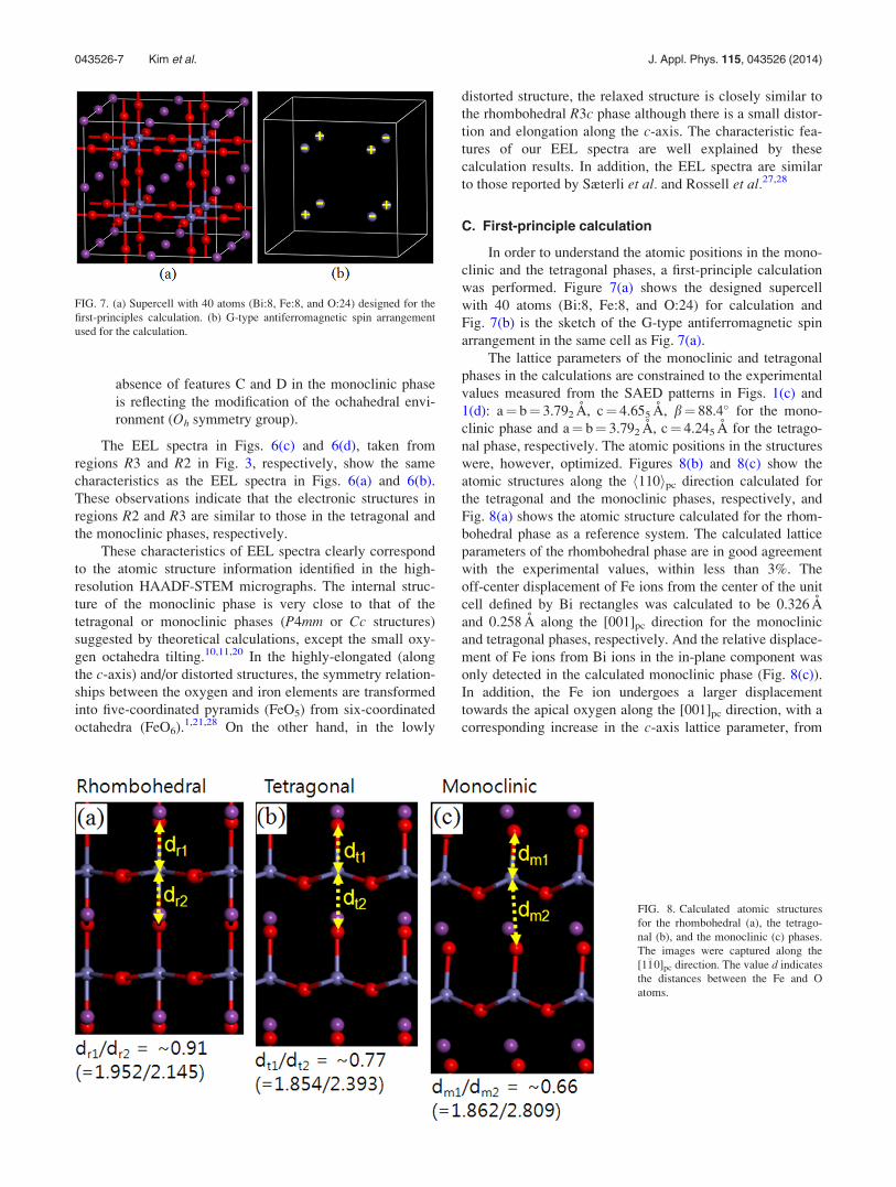
was performed. Figure 7(a) shows the designed supercell
with 40 atoms (Bi:8, Fe:8, and O:24) for calculation and
Fig. 7(b) is the sketch of the G-type antiferromagnetic spin
arrangement in the same cell as Fig. 7(a).
The lattice parameters of the monoclinic and tetragonal
phases in the calculations are constrained to the experimental
values measured from the SAED patterns in Figs. 1(c) and
1(d): a¼ b¼ 3.792 A, c¼ 4.655 A, b¼ 88.4� for the mono-
clinic phase and a¼ b¼ 3.792 A, c¼ 4.245 A for the tetrago-
nal phase, respectively. The atomic positions in the structures
were, however, optimized. Figures 8(b) and 8(c) show the
atomic structures along the h110ipc direction calculated for
the tetragonal and the monoclinic phases, respectively, and
Fig. 8(a) shows the atomic structure calculated for the rhom-
bohedral phase as a reference system. The calculated lattice
parameters of the rhombohedral phase are in good agreement
with the experimental values, within less than 3%. The
off-center displacement of Fe ions from the center of the unit
cell defined by Bi rectangles was calculated to be 0.326 A
and 0.258 A along the [001]pc direction for the monoclinic
and tetragonal phases, respectively. And the relative displace-
ment of Fe ions from Bi ions in the in-plane component was
only detected in the calculated monoclinic phase (Fig. 8(c)).
In addition, the Fe ion undergoes a larger displacement
towards the apical oxygen along the [001]pc direction, with a
corresponding increase in the c-axis lattice parameter, from
FIG. 7. (a) Supercell with 40 atoms (Bi:8, Fe:8, and O:24) designed for the
first-principles calculation. (b) G-type antiferromagnetic spin arrangement
used for the calculation.
FIG. 8. Calculated atomic structures
for the rhombohedral (a), the tetrago-
nal (b), and the monoclinic (c) phases.
The images were captured along the
[1�10]pc direction. The value d indicates
the distances between the Fe and O
atoms.
043526-7 Kim et al. J. Appl. Phys. 115, 043526 (2014)
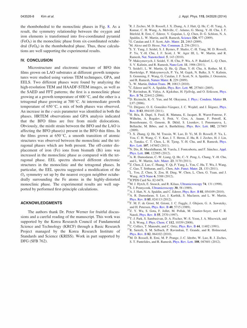
the rhombohedral to the monoclinic phases in Fig. 8. As a
result, the symmetry relationship between the oxygen and
iron elements is transformed into five-coordinated pyramid
(FeO5) in the monoclinic phase from six-coordinated octahe-
dral (FeO6) in the rhombohedral phase. Thus, these calcula-
tions are well supporting the experimental results.
IV. CONCLUSION
Microstructure and electronic structure of BFO thin
films grown on LAO substrates at different growth tempera-
tures were studied using various TEM techniques, GPA, and
EELS. Two different phases were found by analyzing the
high-resolution TEM and HAADF-STEM images, as well as
the SAED and FFT patterns; the first is a monoclinic phase
growing at a growth temperature of 600 �C, and the other is a
tetragonal phase growing at 700 �C. At intermediate growth
temperature of 650 �C, a mix of both phases was observed.
An increase in the c-axis parameter was identified in both the
phases. HRTEM observations and GPA analysis indicated
that the BFO films are free from misfit dislocations.
Obviously, the misfit strain between the BFO and the LAO is
affecting the BFO phase(s) present in the BFO thin films. In
the films grown at 650 �C, a smooth transition of atomic
structures was observed between the monoclinic and the tet-
ragonal phases which are both present. The off-center dis-
placement of iron (Fe) ions from bismuth (Bi) ions was
increased in the monoclinic phase as compared with the tet-
ragonal phase. EEL spectra showed different electronic
structures in the monoclinic and the tetragonal phases. In
particular, the EEL spectra suggested a modification of the
Oh symmetry set up by the nearest oxygen neighbor octahe-
drally surrounding the Fe atoms in the highly-distorted
monoclinic phase. The experimental results are well sup-
ported by performed first-principle calculations.
ACKNOWLEDGMENTS
The authors thank Dr. Peter Werner for fruitful discus-
sions and a careful reading of the manuscript. This work was
supported by the Korea Research Council of Fundamental
Science and Technology (KRCF) through a Basic Research
Project managed by the Korea Research Institute of
Standards and Science (KRISS). Work in part supported by
DFG (SFB 762).
1R. J. Zeches, M. D. Rossell, J. X. Zhang, A. J. Hatt, Q. He, C.-H. Yang, A.
Kumar, C. H. Wang, A. Melville, C. Adamo, G. Sheng, Y.-H. Chu, J. F.
Ihlefeld, R. Erni, C. Ederer, V. Gopalan, L. Q. Chen, D. G. Schlom, N. A.
Spaldin, L. W. Martin, and R. Ramesh, Science 326, 977 (2009).2G. Catalan and J. F. Scott, Adv. Mater. 21, 2463 (2009).3M. Alexe and D. Hesse, Nat. Commun. 2, 256 (2011).4S. Y. Yang, J. Seidel, S. J. Byrnes, P. Shafer, C.-H. Yang, M. D. Rossell,
P. Yu, Y.-H. Chu, J. F. Scott, J. W. Ager III, L. W. Martin, and R.
Ramesh, Nat. Nanotechnol. 5, 143 (2010).5P. Maksymovych, J. Seidel, Y. H. Chu, P. Wu, A. P. Baddorf, L.-Q. Chen,
S. V. Kalinin, and R. Ramesh, Nano Lett. 11, 1906 (2011).6J. Seidel1, L. W. Martin, Q. He, Q. Zhan, Y.-H. Chu, A. Rother, M. E.
Hawkridge, P. Maksymovych, P. Yu, M. Gajek, N. Balke, S. V. Kalinin,
S. Gemming, F. Wang, G. Catalan, J. F. Scott, N. A. Spaldin, J. Orenstein,
and R. Ramesh, Nature Mater. 8, 229 (2009).7L. W. Martin, Dalton Trans. 39, 10813 (2010).8C. Ederer and N. A. Spaldin, Phys. Rev. Lett. 95, 257601 (2005).9P. Ravindran, R. Vidya, A. Kjekshus, H. Fjellvag, and O. Eriksson, Phys.
Rev. B 74, 224412 (2006).10D. Ricinschi, K.-Y. Yun, and M. Okuyama, J. Phys.: Condens. Matter 18,
L97 (2006).11O. Di�eguez, O. E. Gonz�alez-V�azquez, J. C. Wojdeł, and J. �I~niguez, Phys.
Rev. B 83, 094105 (2011).12H. B�ea, B. Dup�e, S. Fusil, R. Mattana, E. Jacquet, B. Warot-Fonrose, F.
Wilhelm, A. Rogalev, S. Petit, V. Cros, A. Anane, F. Petroff, K.
Bouzehouane, G. Geneste, B. Dkhil, S. Lisenkov, I. Ponomareva, L.
Bellaiche, M. Bibes, and A. Barth�el�emy, Phys. Rev. Lett. 102, 217603
(2009).13J. X. Zhang, Q. He, M. Trassin, W. Luo, D. Yi, M. D. Rossell, P. Yu, L.
You, C. H. Wang, C. Y. Kuo, J. T. Heron, Z. Hu, R. J. Zeches, H. J. Lin,
A. Tanaka, C. T. Chen, L. H. Tjeng, Y.-H. Chu, and R. Ramesh, Phys.
Rev. Lett. 107, 147602 (2011).14N. Dix, R. Muralidharan, M. Varela, J. Fontcuberta, and F. S�anchez, Appl.
Phys. Lett. 100, 122905 (2012).15A. R. Damodaran, C.-W. Liang, Q. He, C.-Y. Peng, L. Chang, Y.-H. Chu,
and L. W. Martin, Adv. Mater. 23, 3170 (2011).16Z. Chen, Z. Luo, C. Huang, Y. Qi, P. Yang, L. You, C. Hu, T. Wu, J. Wang,
C. Gao, T. Sritharan, and L. Chen, Adv. Funct. Mater. 21, 133 (2011).17L. You, Z. Chen, X. Zou, H. Ding, W. Chen, L. Chen, G. Yuan, and J.
Wang, ACS Nano 6, 5388 (2012).18JCPDS Card No. 82-0478.19M. J. Hytch, E. Snoeck, and R. Kilaas, Ultramicroscopy 74, 131 (1998).20S. J. Pennycook, Ultramicroscopy 30, 58 (1989).21A. J. Hatt, N. A. Spaldin, and C. Ederer, Phys. Rev. B 81, 054109 (2010).22A. R. Damodaran, S. Lee, J. Karthik, S. Maclaren, and L. W. Martin,
Phys. Rev. B 85, 024113 (2012).23F. M. F. de Groot, M. Grioni, J. C. Fuggle, J. Ghijsen, G. A. Sawatzky,
and H. Petersen, Phys. Rev. B 40, 5715 (1989).24Z. Y. Wu, S. Gota, F. Jollet, M. Pollak, M. Gautier-Soyer, and C. R.
Natoli, Phys. Rev. B 55, 2570 (1997).25T.-J. Park, S. Sambasivan, D. A. Fischer, W.-S. Yoon, J. A. Misewich, and
S. S. Wong, J. Phys. Chem. C 112, 10359 (2008).26C. Colliex, T. Manoubi, and C. Ortiz, Phys. Rev. B 44, 11402 (1991).27R. Sæterli, S. M. Selbach, P. Ravindran, T. Grande, and R. Holmestad,
Phys. Rev. B 82, 064102 (2010).28M. D. Rossell, R. Erni, M. P. Prange, J.-C. Idrobo, W. Luo, R. J. Zeches,
S. T. Pantelides, and R. Ramesh, Phys. Rev. Lett. 108, 047601 (2012).
043526-8 Kim et al. J. Appl. Phys. 115, 043526 (2014)