Microscopical Characterisation of Solid and Biological ... · PDF fileMicroscopical...
35
Microscopical Characterisation of Solid and Biological Materials KOO 065 Also known as “Microanalysis Course” “Okända prov.” Reine Wallenberg, (SEM, TEM) Crispin Hetherington (TEM, EELS) Axel Persson (SEM, TEM) Reza Zamani (TEM) nCHREM, Lund University 1
Transcript of Microscopical Characterisation of Solid and Biological ... · PDF fileMicroscopical...

Microscopical Characterisation of Solid and Biological Materials KOO 065
Also known as “Microanalysis Course” “Okända prov.”
Reine Wallenberg, (SEM, TEM)
Crispin Hetherington (TEM, EELS) Axel Persson (SEM, TEM)
Reza Zamani (TEM)
nCHREM, Lund University 1
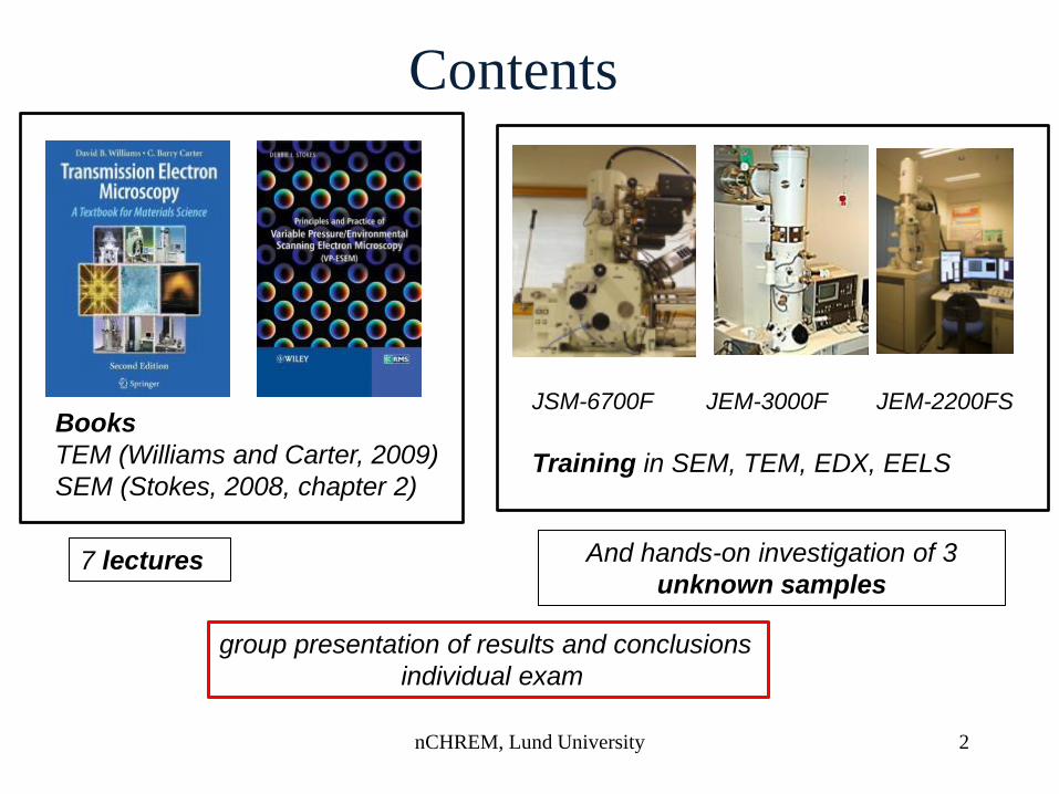
Contents
nCHREM, Lund University 2
JSM-6700F JEM-3000F JEM-2200FS Training in SEM, TEM, EDX, EELS
Books TEM (Williams and Carter, 2009) SEM (Stokes, 2008, chapter 2)
group presentation of results and conclusions individual exam
7 lectures And hands-on investigation of 3 unknown samples

Lectures Library at Materials Chemistry, Monday afternoons
nCHREM, Lund University 3
lecture 1 Introduction and TEM basics lecture 2 SEM lecture 3 EDX (2 week break) lecture 4 EELS and EFTEM lecture 5, 6, 7 TEM (spec prep, HREM, CTF...) possible extras Environmental TEM Image simulation in JEMS Image processing in DigitalMicrograph
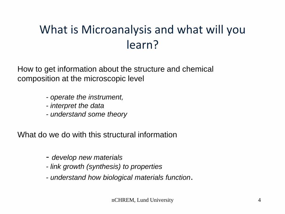
What is Microanalysis and what will you learn?
nCHREM, Lund University 4
How to get information about the structure and chemical composition at the microscopic level - operate the instrument, - interpret the data - understand some theory What do we do with this structural information - develop new materials - link growth (synthesis) to properties - understand how biological materials function.
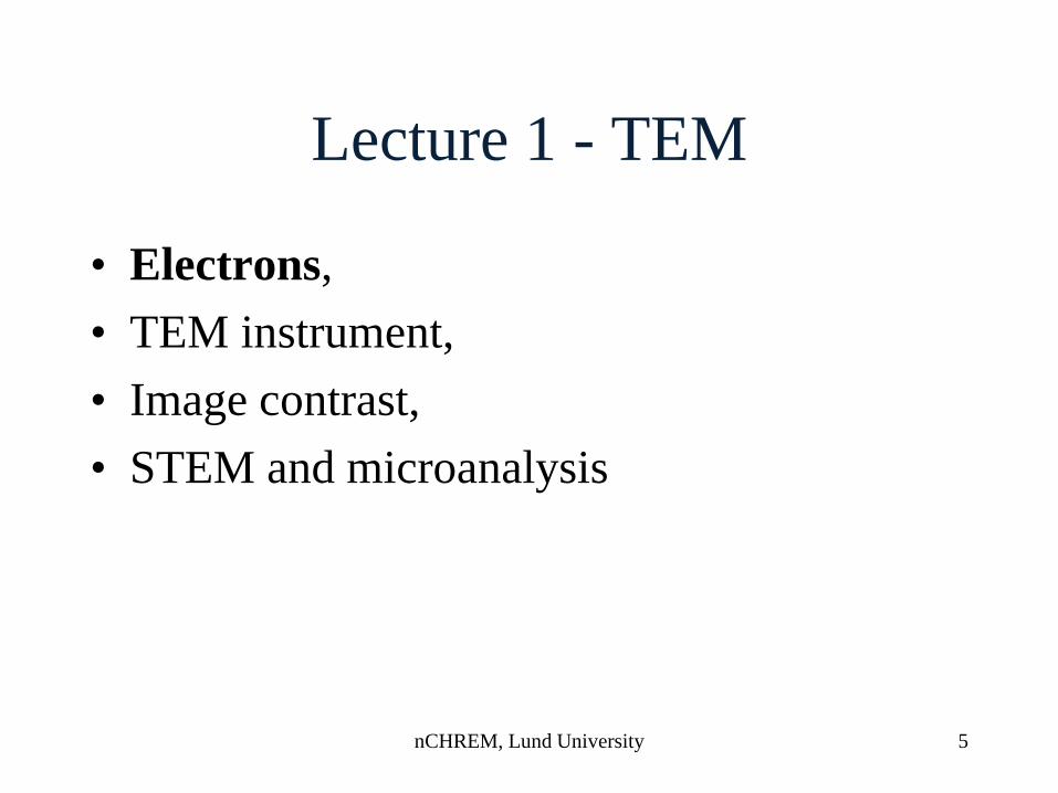
Lecture 1 - TEM
• Electrons, • TEM instrument, • Image contrast, • STEM and microanalysis
nCHREM, Lund University 5

Why do we use electrons for our microscopes? what are the advantages compared to light or X-rays or neutrons?
• charged particles interact strongly with the sample
• charged particles so we can use magnetic lenses to form an image
• short wavelength (0.002nm)
allows imaging at high resolution
do = 0.66 Cs1/4λ3/4
The National Center for HREM, Lund University, Reine Wallenberg
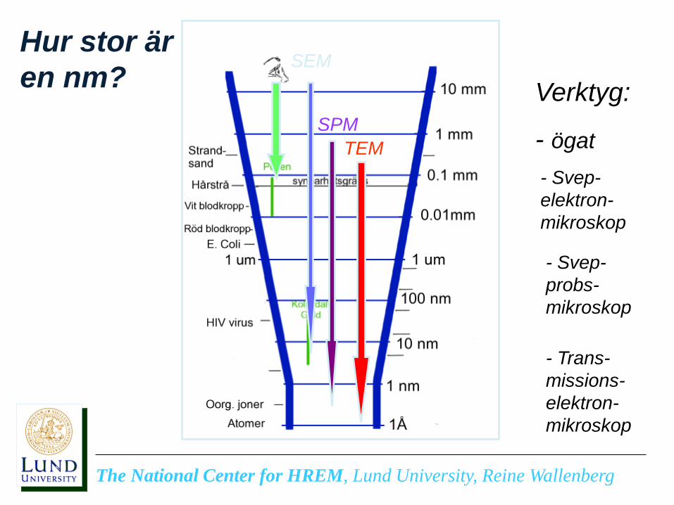
Hur stor är en nm? Verktyg:
- ögat - Svep-elektron-mikroskop
SEM
SPM
- Svep-probs-mikroskop
TEM
- Trans-missions-elektron-mikroskop
nCHREM, Lund University 8
SEM
SEM
SEM
TEM
STEM
STEM STEM TEM
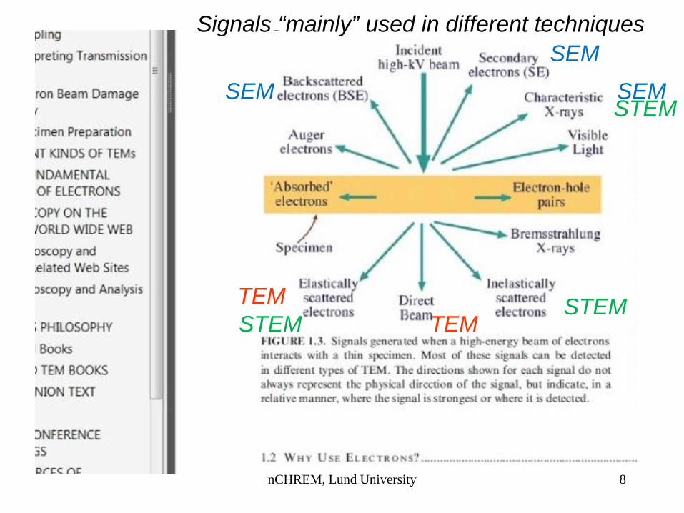
Signals “mainly” used in different techniques

illumination
specimen
lens
camera
Light Microscope Electron Microscope
illumination
specimen
lens
camera

How do we generate electron beam? • thermal emission (W or LaB6 crystal) or
field emission
• Accelerate the electrons by 60-300kV – electrons behave like waves – high kV for resolution – low kV to minimise beam damage
• ~1eV energy spread
– required for imaging and spectroscopy
W

How we configure the beam for imaging or microanalysis?
wide parallel beam or small probe
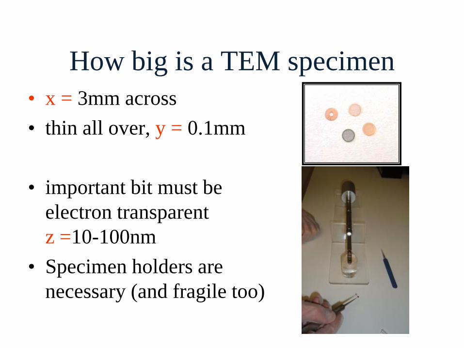
How big is a TEM specimen • x = 3mm across • thin all over, y = 0.1mm
• important bit must be
electron transparent z =10-100nm
• Specimen holders are necessary (and fragile too)
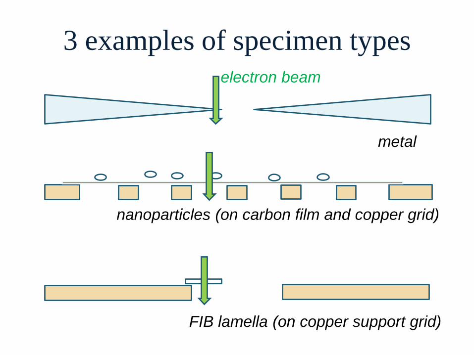
3 examples of specimen types
metal foil
nanoparticles (on carbon film and copper grid)
FIB lamella (on copper support grid)
electron beam

The objective lens: ”heart of the microscope”
• Quality of this lens determines image resolution
• An immersion lens - so astigmatism must be corrected for each sample
• Lens strength usually held in narrow range – alignment and calibrations preserved – change sample height for coarse focus – change lens current for fine focus
resolution limit do = 0.66Cs1/4λ3/4

The objective lens and its aberrations
perfect lens spherical aberration Cs chromatic aberration Cc
To paraphrase Ernst Abbe (1849 – 1905) : ”if you want to understand the microscope, consider the specimen as a diffraction grating and ask, does the diffracted beam get through the lens ok”
resolution limit do = 0.66Cs1/4λ3/4
16
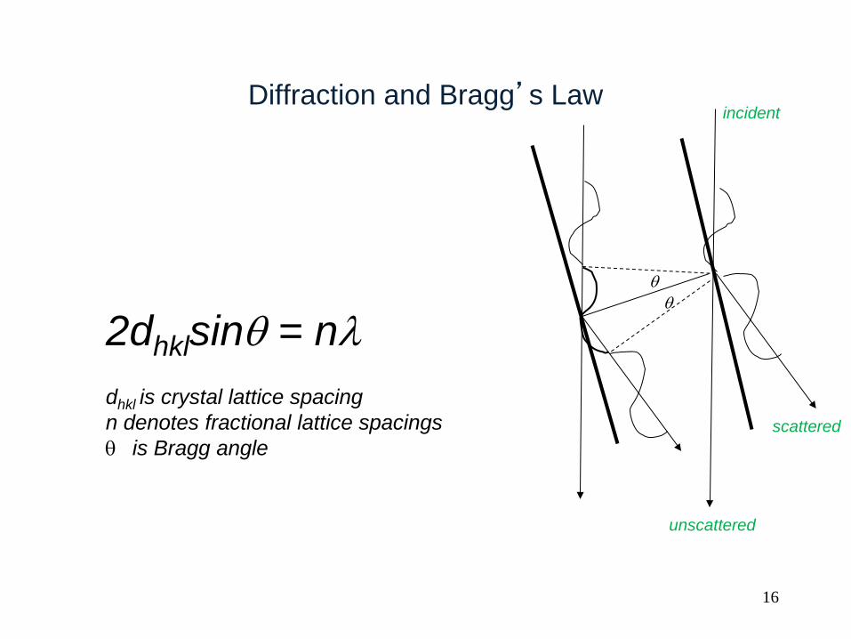
Diffraction and Bragg’s Law
2dhklsinθ = nλ dhkl is crystal lattice spacing n denotes fractional lattice spacings θ is Bragg angle
θ θ
unscattered
scattered
incident

And the rest of the lenses.... • we can change
magnification of the image

..or switch between imaging and diffraction

camera
Transmission Electron Microscope
accelerator
condenser lens
specimen holder
electron gun
beam deflectors (eg scan coils)
objective lens
objective aperture
projector lens
Xray spectrometer
intermediate aperture
condenser aperture
EELS spectrometer

thin ”electron transparent” sample
nCHREM, Lund University 20
In TEM, we illuminate the sample uniformly and we use thin samples that transmit the fast electrons. A good lens focusses all the scattered and unscattered electrons from point A on the sample onto the point B on the camera... Err!?
sample
lens
camera
incident beam
A
B

Mass-thickness contrast • The objective aperture
is placed around the forward-scattered beam, excluding the scattered electrons.
sample
image

Mass-thickness contrast
nCHREM, Lund University 22

23
Overview of Image Contrast
Mass/thickness “absorption”
(aperture in diffraction plane)
Diffraction contrast
spec
imen
im
age
(aperture in diffraction plane & energy filter)
elec
tron
be
am
phase contrast
(contrast transfer function in diffraction plane)
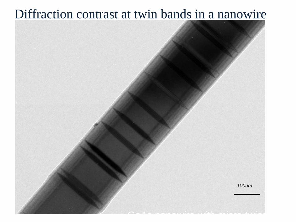
Diffraction contrast at twin bands in a nanowire
100nm
GaAs nanowire with micro twins

25
diffraction contrast to reveal line defects in an interface
dark field micrographs can identify type of defect

26
phase object
incident plane wave
transmitted wave note: phase of wavefront has changed - but amplitude unaffected
q(x) = exp{-iσϕ(x)} σ = interaction constant ϕ = projected potential
atoms

HREM – phase contrast
atomic columns change the phase of the electron beam . objective lens ”defects” (focus, Cs) generate phase contrast.
100nm

Schematic diagram of the objective lens area showing the positions of the objective- and selected
area apertures
your turn to draw simple version

TEM mode STEM mode
condenser lens
objective lens
TEM and STEM - beam alignment, lens astigmatism, focus...
sample

The National Center for HREM, Lund University, Reine Wallenberg
STEM with analytical electron microscopy (AEM)
HAADF, high angle annular dark field detector to record signal for STEM image
electron spectrometer for electron energy loss (STEM) and energy filtered images (TEM)
Xray spectrometer for elemental analysis (STEM)
nCHREM, Lund University 31
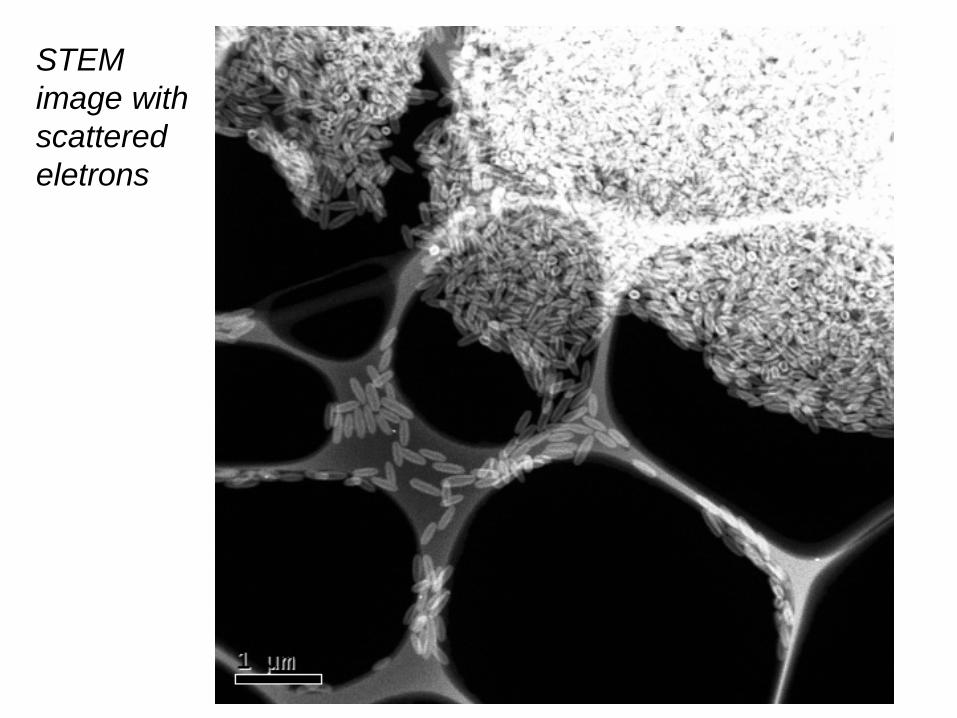
STEM image with scattered eletrons
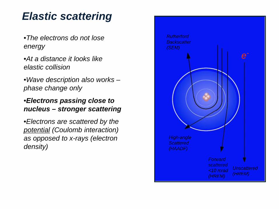
Elastic scattering
•The electrons do not lose energy
•At a distance it looks like elastic collision
•Wave description also works – phase change only
•Electrons passing close to nucleus – stronger scattering
•Electrons are scattered by the potential (Coulomb interaction) as opposed to x-rays (electron density)
Unscattered (HREM)
Forward scattered <10 mrad (HREM)
High-angle Scattered (HAADF)
Rutherford Backscatter (SEM)
e-

Inelastic scattering
The chemists microscope! Incoming electrons ionize the atom (core-shell excitation). Ionization energies depend on which element.
To lose the extra energy, the atom emits an x-ray (XEDS)
The energy loss of the transmitted electron can be measured (EELS)
33 nCHREM, Lund University

A quick word about looking after your TEM • Good environment
– stable floors – quiet room
• Good vacuum – clean specimens – clean holder
• Safety
– X rays, high kV, Be-coated holders, liquid nitrogen

Good practice for hands-on working
• good sharp tweezers to handle grids
• pre-inspect 3mm sample in light microscope/i-phone
• take good notes in your lab book
• understand alignment, but don’t overdo it
• do insert objective aperture for standard images
• take low magnification image of general area
notebook