Microprocessor Ramesh S Gaonkar
25
Micro Processors and Microcontrollers
Transcript of Microprocessor Ramesh S Gaonkar

8/3/2019 Microprocessor Ramesh S Gaonkar
http://slidepdf.com/reader/full/microprocessor-ramesh-s-gaonkar 1/25
Micro Processors and Microcontrollers

8/3/2019 Microprocessor Ramesh S Gaonkar
http://slidepdf.com/reader/full/microprocessor-ramesh-s-gaonkar 2/25
8085 INTRODUCTIONThe features of INTEL 8085 are :
It is an 8 bit processor.
It is a single chip N-MOS device with 40 pins.
It has multiplexed address and data bus.(AD0-AD7).
It works on 5 Volt dc power supply.
The maximum clock frequency is 3 MHz whileminimum frequency is 500kHz.
It provides 74 instructions with 5 different addressing
modes.

8/3/2019 Microprocessor Ramesh S Gaonkar
http://slidepdf.com/reader/full/microprocessor-ramesh-s-gaonkar 3/25
8085 INTRODUCTION
It provides 16 address lines so it can access 2^16
=64K bytes of memory.
It generates 8 bit I/O address so it can access
2^8=256 input ports.
It provides 5 hardware interrupts:TRAP, RST 5.5,
RST 6.5, RST 7.5,INTR.
It provides Acc ,one flag register ,6 general
purpose registers and two special purpose
registers(SP,PC).
It provides serial lines SID ,SOD.So serial
peripherals can be interfaced with 8085 directly.

8/3/2019 Microprocessor Ramesh S Gaonkar
http://slidepdf.com/reader/full/microprocessor-ramesh-s-gaonkar 4/25
8085 PIN DIAGRAM

8/3/2019 Microprocessor Ramesh S Gaonkar
http://slidepdf.com/reader/full/microprocessor-ramesh-s-gaonkar 5/25
Pins
Power Supply: +5 V
Frequency
Generator isconnected to
those pins
Input/Output/
Memory
Read
Write
Address latchMultiplexed
Address DataBus
Enable
AddressBus

8/3/2019 Microprocessor Ramesh S Gaonkar
http://slidepdf.com/reader/full/microprocessor-ramesh-s-gaonkar 6/25

8/3/2019 Microprocessor Ramesh S Gaonkar
http://slidepdf.com/reader/full/microprocessor-ramesh-s-gaonkar 7/25
8085 PIN DESCRIPTIONSome important pins are :
AD0-AD7: Multiplexed Address and data lines.
A8-A15: Tri-stated higher order address lines. ALE: Address latch enable is an output signal.It goes high
when operation is started by processor .
S0,S1: These are the status signals used to indicate type of
operation. RD¯: Read is active low input signal used to read data from I/O
device or memory.
WR¯:Write is an active low output signal used write data on
memory or an I/O device.

8/3/2019 Microprocessor Ramesh S Gaonkar
http://slidepdf.com/reader/full/microprocessor-ramesh-s-gaonkar 8/25
8085 PIN DESCRIPTION READY:This an output signal used to check the status of
output device.If it is low, µP will WAIT until it is high.
TRAP:It is an Edge triggered highest priority , non maskable interrupt. After TRAP, restart occurs and executionstarts from address 0024H.
RST5.5,6.5,7.5:These are maskable interrupts and havelow priority than TRAP.
INTR¯&INTA:INTR is a interrupt request signal after whichµP generates INTA or interrupt acknowledge signal.
IO/M¯:This is output pin or signal used to indicatewhether 8085 is working in I/O mode(IO/M¯=1) orMemory mode(IO/M¯=0 ).

8/3/2019 Microprocessor Ramesh S Gaonkar
http://slidepdf.com/reader/full/microprocessor-ramesh-s-gaonkar 9/25

8/3/2019 Microprocessor Ramesh S Gaonkar
http://slidepdf.com/reader/full/microprocessor-ramesh-s-gaonkar 10/25
8085 ARCHITECTURE
8/3/2019 Microprocessor Ramesh S Gaonkar
http://slidepdf.com/reader/full/microprocessor-ramesh-s-gaonkar 11/25
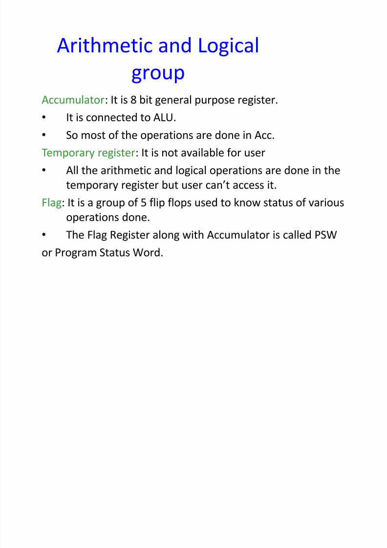
Arithmetic and Logical
groupAccumulator: It is 8 bit general purpose register.
It is connected to ALU.
So most of the operations are done in Acc.Temporary register: It is not available for user
All the arithmetic and logical operations are done in the
temporary register but user cant access it.
Flag: It is a group of 5 flip flops used to know status of variousoperations done.
The Flag Register along with Accumulator is called PSW
or Program Status Word.

8/3/2019 Microprocessor Ramesh S Gaonkar
http://slidepdf.com/reader/full/microprocessor-ramesh-s-gaonkar 12/25
Flag Register
- 8 bit register - shows the status of the microprocessor before/after an
operation
- S (sign flag), Z (zero flag), AC (auxillary carry flag), P (parity flag) &
CY (carry flag)
D7 D6 D5 D4 D3 D2 D1 D0
S Z X AC X P X CY
- Sign Flag
Used for indicating the sign of the data in the accumulator The sign flag is set if negative (1 - negative)
The sign flag is reset if positive (0 -positive)

8/3/2019 Microprocessor Ramesh S Gaonkar
http://slidepdf.com/reader/full/microprocessor-ramesh-s-gaonkar 13/25
Zero Flag
- Is set if result obtained after an operation is 0- Is set following an increment or decrement operation of that register
10110011
Carry Flag
+ 01001101
---------------
100000000
- Is set if there is a carry or borrow from arithmetic operation
1011 0101 1011 0101
+ 0110 1100 - 1100 1100
--------------- ---------------
Carry 1 0010 0001 Borrow 1 1110 1001

8/3/2019 Microprocessor Ramesh S Gaonkar
http://slidepdf.com/reader/full/microprocessor-ramesh-s-gaonkar 14/25
Auxillary Carry Flag
- Is set if there is a carry out of bit 3
Parity Flag
- Is set if parity is even
- Is cleared if parity is odd

8/3/2019 Microprocessor Ramesh S Gaonkar
http://slidepdf.com/reader/full/microprocessor-ramesh-s-gaonkar 15/25
Register Group
Temporary registers (W,Z):These are not
available for user. These are loaded only when
there is an operation being performed.
General purpose:There are six general purpose
registers in 8085 namely B,C,D,E,H,L.These are
used for various data manipulations.
Special purpose :There are two special purposeregisters in 8085:
1. SP :Stack Pointer.
2. PC:Program Counter.

8/3/2019 Microprocessor Ramesh S Gaonkar
http://slidepdf.com/reader/full/microprocessor-ramesh-s-gaonkar 16/25
Registers
- General Purpose Registers B, C, D, E, H & L (8 bit registers)
Can be used singly
Or can be used as 16 bit register pairs- BC, DE, HL
H & L can be used as a data pointer (holds memoryaddress)
Accumulator Flags
- Special Purpose Registers
Accumulator (8 bit register)
- Store 8 bit data- Store the result of an operation
- Store 8 bit data during I/O transfer
B C
D E
H L
Program Counter
Stack Pointer
Address 16 8 Data

8/3/2019 Microprocessor Ramesh S Gaonkar
http://slidepdf.com/reader/full/microprocessor-ramesh-s-gaonkar 17/25
Register GroupStack Pointer: This is a temporary storage memory 16 bit register.
Since there are only 6 general purpose registers, there is a need
to reuse them .
Whenever stack is to be used previous values are PUSHED on
stack and then after the program is over these values are
POPED back.
Program Counter: It is 16 bit register used to point the location
from which the next instruction is to be fetched.
When a single byte instruction is executed PC is automatically
incremented by 1.
Upon reset PC contents are set to 0000H and next instruction is
fetched onwards.

8/3/2019 Microprocessor Ramesh S Gaonkar
http://slidepdf.com/reader/full/microprocessor-ramesh-s-gaonkar 18/25
INSTRUCTION
REGISTER,DECODER &CONTROL
Instruction register:When an instruction is fetched , it is
executed in instruction register.This register takes the
Opcode value only.
Instruction decoder: It decodes the instruction from
instruction register and then to control block.
Timing and control:This is the control section of µP.Itaccepts clock input .

8/3/2019 Microprocessor Ramesh S Gaonkar
http://slidepdf.com/reader/full/microprocessor-ramesh-s-gaonkar 19/25
INTERRUPT CONTROL
It accepts different interrupts like TRAP
INT5.5,6.5,7.5and INTR.
SERIAL IO CONTROLGROUP
It is used to accept the serial 1 bit data byusing SID and SOD signals and it can be
performed by using SIM & RIM
instructions.

8/3/2019 Microprocessor Ramesh S Gaonkar
http://slidepdf.com/reader/full/microprocessor-ramesh-s-gaonkar 20/25

8/3/2019 Microprocessor Ramesh S Gaonkar
http://slidepdf.com/reader/full/microprocessor-ramesh-s-gaonkar 21/25
The Address and Data Busses The address bus has 8 signal lines A8 - A15which are unidirectional.
The other 8 address bits are multiplexed (timeshared) with the 8 data bits.
- So, the bits AD0 - AD7 are bi-directional and serve asA0 - A7 and D0 - D7 at the same time.
During the execution of the instruction, these lines carry the
address bits during the early part, then during the late parts of the execution, they carry the 8 data bits.
- In order to separate the address from the data, we canuse a latch to save the value before the function of the
bits changes.

8/3/2019 Microprocessor Ramesh S Gaonkar
http://slidepdf.com/reader/full/microprocessor-ramesh-s-gaonkar 22/25
Demultiplexing AD7-AD0
- From the above description, it becomes obvious
that the AD7- AD0 lines are serving a dual purposeand that they need to be demultiplexed to get all theinformation.
- The high order bits of the address remain on the
bus for three clock periods. However, the low order bits remain for only one clock period and theywould be lost if they are not saved externally. Also,notice that the low order bits of the addressdisappear when they are needed most.
- To make sure we have the entire address for thefull three clock cycles, we will use an external latchto save the value of AD7- AD0 when it is carryingthe address bits. We use the ALE signal to enable
this latch.

8/3/2019 Microprocessor Ramesh S Gaonkar
http://slidepdf.com/reader/full/microprocessor-ramesh-s-gaonkar 23/25
Demultiplexing AD7-AD0
8085 A15- A8
ALE
AD7- AD0Latch
A 7 - A 0
D7- D0
- Given that ALE operates as a pulse during T1, we will
be able to latch the address. Then when ALE goes low,the address is saved and the AD7- AD0 lines can be
used for their purpose as the bi-directional data lines.

8/3/2019 Microprocessor Ramesh S Gaonkar
http://slidepdf.com/reader/full/microprocessor-ramesh-s-gaonkar 24/25
Demultiplexing the Bus AD7 - AD0
The high order address is placed on the address bus and hold for 3 clk
periods,
The low order address is lost after the first clk period, this address
needs to be hold however we need to use latch The address AD7 - AD0 is connected as inputs to the latch 74LS373.
The ALE signal is connected to the enable (G) pin of the latch and the
OC - Output control - of the latch is grounded

8/3/2019 Microprocessor Ramesh S Gaonkar
http://slidepdf.com/reader/full/microprocessor-ramesh-s-gaonkar 25/25
The Overall Picture
Putting all of the concepts together, we get:
8085
A15-A8
ALE
Latch AD7- AD0 A 7 - A 0
Chip SelectionA15- A10Circuit
CS
A9- A0 1K ByteMemory
Chip
WR RD IO/M D7- D0
RD
WR