Piezoelectric Micromachined Ultrasound Transducers ( pMUTs )

Micromachined Chopper for Mobile Infrared
Spectroscopy
Andrea Angelo Poli
April 17, 2005
Abstract
A micromachined chopper has been designed to improve mobile in-frared spectroscopy measurements. It works in the spectral range of 2–5 µm, has an aperture of 0.5 cm, operates at rates exceeding 100 Hz, han-dles temperatures up to 200 C, and blocks infrared, in its off state, wellenough to provide a 100:1 contrast ratio. Existing chopper designs arereviewed and four actuation methods are considered: magnetic, thermal,electrostatic, and piezoelectric. Damping due to Couette flow is consid-ered in both the continuous and Knudsen regimes.
Contents
1 Introduction 2
2 Application Requirements 4
3 Concept Generation and Selection 63.1 Shuttering Concepts . . . . . . . . . . . . . . . . . . . . . . . . . 83.2 Actuator Concepts . . . . . . . . . . . . . . . . . . . . . . . . . . 12
3.2.1 Electrostatic . . . . . . . . . . . . . . . . . . . . . . . . . 153.2.2 Thermal . . . . . . . . . . . . . . . . . . . . . . . . . . . . 153.2.3 Magnetic . . . . . . . . . . . . . . . . . . . . . . . . . . . 153.2.4 Piezoelectric . . . . . . . . . . . . . . . . . . . . . . . . . 163.2.5 Actuator Selection . . . . . . . . . . . . . . . . . . . . . . 16
4 Design 174.1 Mechanics . . . . . . . . . . . . . . . . . . . . . . . . . . . . . . . 174.2 Dynamics . . . . . . . . . . . . . . . . . . . . . . . . . . . . . . . 194.3 Electrical . . . . . . . . . . . . . . . . . . . . . . . . . . . . . . . 194.4 Thermal . . . . . . . . . . . . . . . . . . . . . . . . . . . . . . . . 204.5 Optics . . . . . . . . . . . . . . . . . . . . . . . . . . . . . . . . . 204.6 Testing . . . . . . . . . . . . . . . . . . . . . . . . . . . . . . . . 224.7 Processing and Costs . . . . . . . . . . . . . . . . . . . . . . . . . 22
1

5 Modelling 275.1 Layout . . . . . . . . . . . . . . . . . . . . . . . . . . . . . . . . . 275.2 Mechanical . . . . . . . . . . . . . . . . . . . . . . . . . . . . . . 275.3 Dynamic . . . . . . . . . . . . . . . . . . . . . . . . . . . . . . . . 285.4 Modelling Recap . . . . . . . . . . . . . . . . . . . . . . . . . . . 28
6 Summary 30
7 Acknowledgements 30
A Layout Definition 30A.1 Individual Masks . . . . . . . . . . . . . . . . . . . . . . . . . . . 32A.2 Process Definition File . . . . . . . . . . . . . . . . . . . . . . . . 32A.3 Mask Generating Script . . . . . . . . . . . . . . . . . . . . . . . 33
B Finite Element Script 35
1 Introduction
Emissions from internal combustion vehicles are routinely measured by passingtheir exhaust through laboratory instruments while operating on a dynamome-ter. However, these measurements are not representative of in-use emissionssince driving conditions, vehicle age, and maintenance, affect them in practice.To allow more representative measurements, in-use emissions instruments weredeveloped. They are trunk-mounted and take up a considerable fraction of thatspace (Fig. 1). Motivated by the U.S. EPA, which has said that it will requiremanufacturers to perform on-vehicle testing in the near future [1], manufac-turers of in-use emissions systems are working to reduce the size, power, andcomplexity of their systems while increasing their reliability.
Among the instruments within these analysis systems is a nondispersive in-frared spectrometer [2]. It operates by passing a small band of infrared radiationthrough both a reference chamber and a sampling chamber. The spectral rangeof the radiation is chosen to coincide with the molecular absorptions of thedesired analyte. By examining the difference between the absorption in eachchamber, the analyte concentration can be determined (Fig. 2).
One problem in infrared spectroscopy is that the detector responds not onlyto radiation from the source, but also to stray radiation (blackbody) generatedwhen hot exhaust (>300 C) heats the spectrometer. This unwanted radiationvaries, particularly during warm up, and interferes with the desired signal. Un-fortunately, reliable measurements are most important at this very time becausea vehicle produces its worst emissions then.
The effects of stray radiation can be mitigated by extinguishing the sourcein order to isolate, measure, and subtract the remaining radiation. This canbe done more readily by modulating the spectrometer’s radiation source morerapidly than the instrument’s response rate.
2

Figure 1: Installed Spectroscopy Sys-tem [1].
Figure 2: Nondispersive infrared spectrometer sche-matic
3
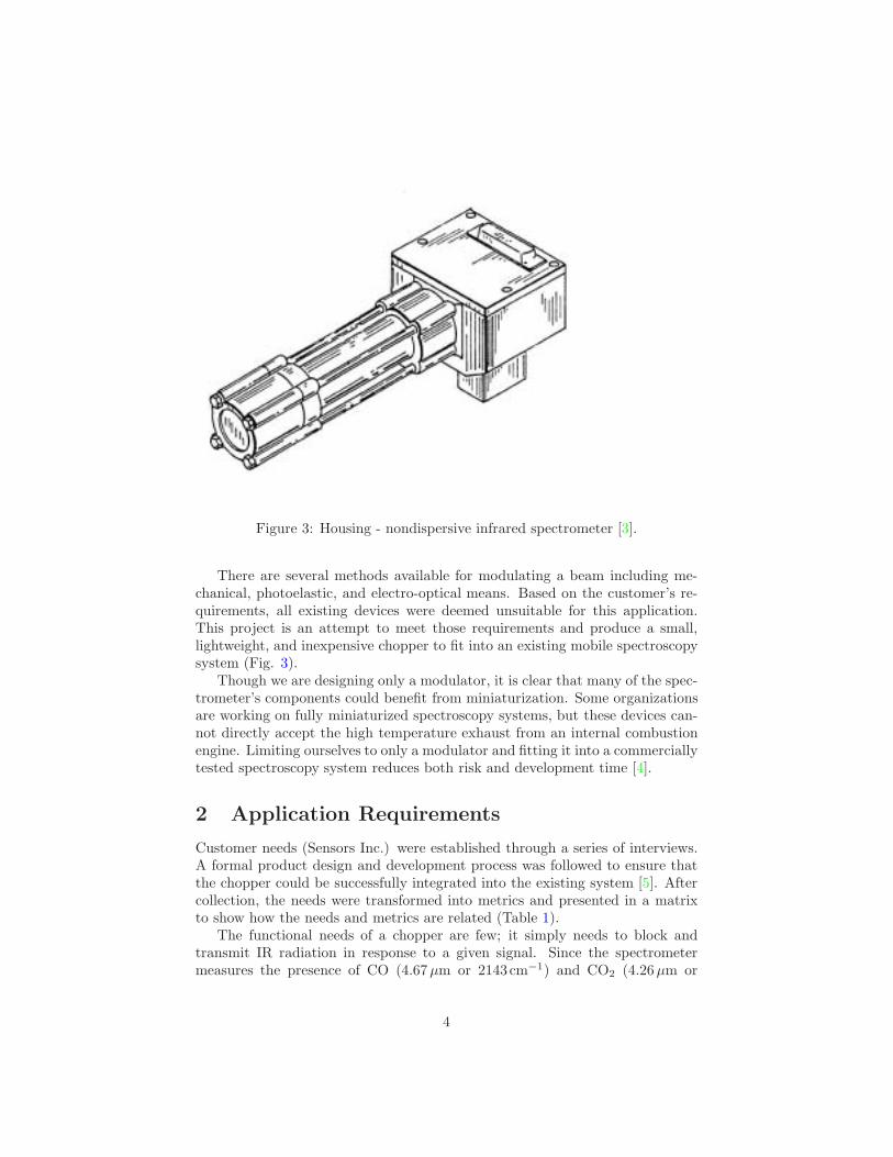
Figure 3: Housing - nondispersive infrared spectrometer [3].
There are several methods available for modulating a beam including me-chanical, photoelastic, and electro-optical means. Based on the customer’s re-quirements, all existing devices were deemed unsuitable for this application.This project is an attempt to meet those requirements and produce a small,lightweight, and inexpensive chopper to fit into an existing mobile spectroscopysystem (Fig. 3).
Though we are designing only a modulator, it is clear that many of the spec-trometer’s components could benefit from miniaturization. Some organizationsare working on fully miniaturized spectroscopy systems, but these devices can-not directly accept the high temperature exhaust from an internal combustionengine. Limiting ourselves to only a modulator and fitting it into a commerciallytested spectroscopy system reduces both risk and development time [4].
2 Application Requirements
Customer needs (Sensors Inc.) were established through a series of interviews.A formal product design and development process was followed to ensure thatthe chopper could be successfully integrated into the existing system [5]. Aftercollection, the needs were transformed into metrics and presented in a matrixto show how the needs and metrics are related (Table 1).
The functional needs of a chopper are few; it simply needs to block andtransmit IR radiation in response to a given signal. Since the spectrometermeasures the presence of CO (4.67µm or 2143cm−1) and CO2 (4.26µm or
4

Table 1: Customer Needs-Metrics Matrix
The chopper Spec
tral
Ran
ge(µ
m)
Ape
rtur
esi
ze(c
m2)
Tra
nsm
issi
on(%
)
Con
tras
tR
atio
Freq
uenc
yR
espo
nse
(Hz)
Ope
rati
ngTem
p.(
)
Vib
ration
(G2·H
z−1)
Vol
tage
(V)
Cur
rent
(mA
)
Pow
er(m
W)
Pro
toty
peC
ost
(US
)
transmits desired radiation • • •blocks desired radiation •switches quickly between states •operates normally at temperature •operates normally under vibration •operates on available voltage •operates on available current •operates on available power •has low prototype costs •interfaces easily to the driving signalinstalls easily into the spectrometeris normally closedis easy to test at the wafer level
5
(a) rotatingwheel
(b) reso-nantbeam
(c) electro-optic
(d) photo-elastic
Figure 4: Examples of commercially available choppers [Boston Electronics].
2349 cm−1), these molecular absorptions determine the required spectral rangeof the spectrometer’s components. We must also ensure that chopper operatesrobustly in the automotive environment. It will be exposed to road vibrationsand temperatures as high as 200 C since the device is near, but not in contactwith, the exhaust gas (>300 C). Another requirement for the chopper is thatit operate from CMOS compatible voltages and currents. Manufacturing andtesting are considered early in the design phase by specifying that the devicemust be easy to build, test, and insert into the existing spectroscopy system.Finally, the prototype cost must be low enough to make it attractive to build.
Most of the needs listed in Table 1 correspond to a single metric: e.g., theneed for fast switching between states corresponds only to frequency response.Other needs, such as the need to transmit the desired radiation, are connectedto multiple metrics: transmitting the desired radiation requires the chopper topass the specified spectral range, through the specified aperture, while ensuringthat enough of the incoming light is transmitted.
There are many commercially available optical choppers including those thatutilize rotating wheels, resonant beams, liquid crystals, and the photoelasticeffect (Fig. 4). However, they are either large, use significant power, or donot work in the desired spectral range. For example, the rotating chopper islarge and consumes over 10 watts of power. The inexpensive resonant beamchopper also consumes significant space and power - and it only operates ata single frequency. Though most these problems have been overcome in theliquid crystal chopper, they do not yet operate in the infrared. A comparisonbetween commercially available choppers was performed and summarized inTable 2 along with the final specifications for our device.
3 Concept Generation and Selection
The function of the chopper is simply to modulate the incoming infrared beam.To do so, it must stop and then pass infrared radiation in response to a signal.The inputs, functions, and outputs are shown in Figure 5. In this simplifieddiagram, continuous infrared radiation is directed into the device along with
6

Table 2: Chopper benchmarking with final specificationsSpecs Units Rotating [6] Beam Liquid Crystal PEM [7]
Spectral Range 2–5 µm no limit no limit 0.4–0.7 0.5–18Aperture size >0.5 cm 1.4Transmission >30 % 100 80Contrast Ratio >50:1Operating Frequency >100 Hz 1000(fixed) 50,000(fixed)Operating Temp - Max. >200 C 200Vibration resistance >1 G2 · Hz−1 <0.1 <0.1Voltage <15 VCurrent <20 mAPower <100 mW 12,000 0.3prototype costs <10,000 US
Unit price < 200 US 300 10,000Size of optical head <10x10x5 mm 50x30x30
7

Figure 5: Functional Diagram
electrical energy, which performs the desired switching, along with a signal,which initiates the switching. The device blocks or transmits the incomingradiation to produce a modulated infrared beam. The diagram is helpful ingenerating concepts for the device since it is easy to brainstorm for physicalmechanisms that might accomplish each function — combinations then lead tomany possibilities.
Consideration of this diagram also led us to combine the electrical signaland power into a single input. This decision is consistent with partitioning thesystem into separate modules for the electronics and electro-mechanical subsys-tems, rather than making a monolithic system. It allows us to focus only onelectro-mechanical portion of the system. The blocking and transmitting of radi-ation are complementary and are simply a form of modulation. The modulationcan be carried out by electro-optic, photoelastic, or mechanical means, but weselect the later because it is most amenable to microelectronic manufacturingmethods.
3.1 Shuttering Concepts
In addition to the mechanical shuttering concepts demonstrated in commer-cially available choppers, we now consider other mechanical concepts from themicromaching literature. We focus on devices that transmit the desired beam(rather than reflect or diffract, since these lead to complicated folded-beam ge-ometries). This will allow us to see the variety of devices that are possible andhelp us in selecting the shuttering concept for our application. Choppers can bedivided into two classes based on the orientation of the optical axis with respectto the substrate upon which they are manufactured. Devices that accept lightfrom an optical fiber are typically arranged with the optical axis in the plane ofthe substrate (e.g., Figure 6). However, in-plane operation severely limits thedevice’s aperture size.
Much larger apertures can be accommodated by orienting the optical axisperpendicular to the substrate. One early device of this type utilizes a torsionalhinge created in (110) oriented silicon. An interesting feature is that the tor-sional shutters can be electrostatically actuated to flip out of the optical path toallow light to pass (Figure 7). A more complex version on this concept, called amicroshutter array, is intended for the Next Generation Space Telescope [12]. It
8

Figure 6: In-plane shutter — the pointed tip blocks light entering from the right[8].
Figure 7: Torsional Shutter [9].
consists of two layers of torsionally-hinged and magnetically susceptible shutterson (100) oriented silicon (Figure 8). By passing a permanent magnet beneath asegment of the shutter, the two layers are magnetized and drawn into contact.Then, a voltage electrostatically locks corresponding shutters together. The ad-dressed shutters remain stuck together and they open as the bottom layer isshifted to deflect the torsional hinges and create a clear path for the incomingradiation. The device was designed to maximize the effective array of the array(approx. 80%).
Another design, fashioned as an electronic eyelid, rolls and unrolls a thinfilm to effect shuttering. It initially rolls up after manufacturing in response toresidual stresses. The shutter is unrolled by actuating it with a high voltage(approx. 200V) (Figure 9). The yield of these devices is low (<80%) and theyfall far outside our our requirement for CMOS compatible voltages.
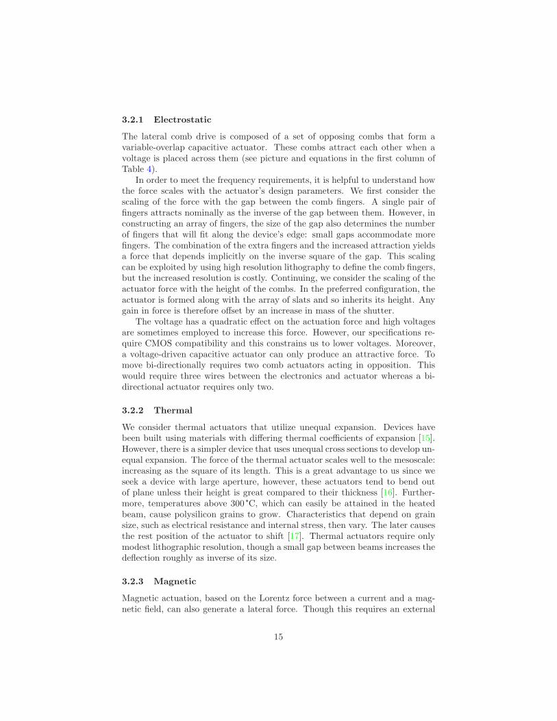
The final example, one of the earliest micromachined choppers, used a solidshutter that was laterally actuated [14]. Though it is possible to scale the solidshutter (Figure 10) up to the millimeter scale, it quickly becomes difficult tomove such a massive shutter. All of the shuttering mechanisms, from commercial
9
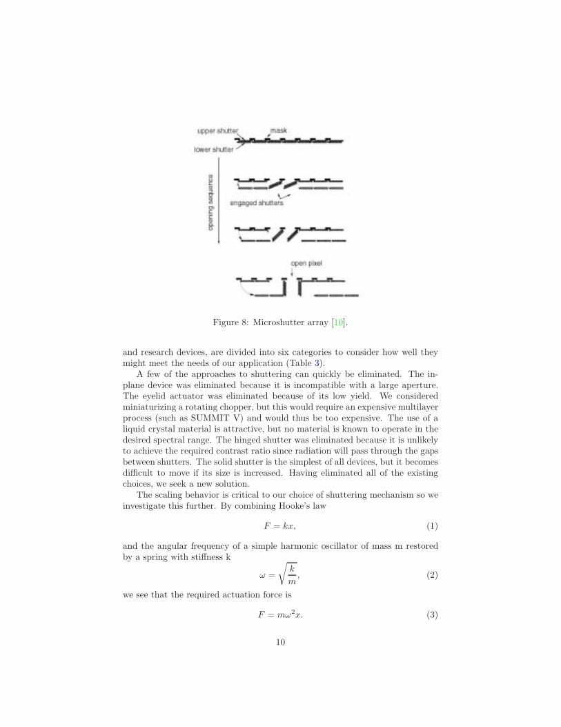
Figure 8: Microshutter array [10].
and research devices, are divided into six categories to consider how well theymight meet the needs of our application (Table 3).
A few of the approaches to shuttering can quickly be eliminated. The in-plane device was eliminated because it is incompatible with a large aperture.The eyelid actuator was eliminated because of its low yield. We consideredminiaturizing a rotating chopper, but this would require an expensive multilayerprocess (such as SUMMIT V) and would thus be too expensive. The use of aliquid crystal material is attractive, but no material is known to operate in thedesired spectral range. The hinged shutter was eliminated because it is unlikelyto achieve the required contrast ratio since radiation will pass through the gapsbetween shutters. The solid shutter is the simplest of all devices, but it becomesdifficult to move if its size is increased. Having eliminated all of the existingchoices, we seek a new solution.
The scaling behavior is critical to our choice of shuttering mechanism so weinvestigate this further. By combining Hooke’s law
F = kx, (1)
and the angular frequency of a simple harmonic oscillator of mass m restoredby a spring with stiffness k
ω =
√k
m, (2)
we see that the required actuation force is
F = mω2x. (3)
10
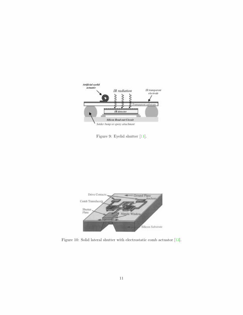
Figure 9: Eyelid shutter [11].
Figure 10: Solid lateral shutter with electrostatic comb actuator [13].
11

Figure 11: Movable slat design with comb actuator (quartered by its two planesof symmetry).
As we scale a solid shutter, while holding it’s thickness fixed, its mass increasesas the square of the length. At the same time, the displacement required tofully retract the solid shutter increases. The result is that the required forcescales as the cube of the shutter width.
However, the required displacement can be greatly reduced by perforatingthe solid shutter and adding a layer of stationary slats to block the light (Figure11). This permits full opening of the shutter with movement of only a singleslat’s width. A drawback is that at least half of the light will be blocked bythe slats. Still, the scheme will allow us to meet all the required specificationsand, most importantly, permits a centimeter sized aperture with a displacementof only tens of microns. An entry was added to the table for this new design(Table 3). The new design was also rated high because the moveable and sta-tionary slats are self-aligned (Figure 14) and so ought to block radiation well.Additionally, the design lends itself to being stiffly attached to the substrate viaa spring to provide the desired vibration resistance. Finally, the simple designoffers a low risk of failure. In Figure 11, the concept is illustrated using a lat-eral comb actuator. Electrostatic actuation is used for illustration only; a widerconsideration of actuator mechanisms follows.
3.2 Actuator Concepts
Having settled on a moving array of slats to block the radiation, we limit our-selves to lateral actuation schemes. Four physical mechanisms were considered:electrostatic, thermal, magnetic, and piezoelectric. Each type can be realizedin multiple ways, but for each of them we present only a single preferred con-figuration.
12

Table 3: Concept Screening - Shutter Mechanisms
Selection CriteriaConcepts
moveable reflector/absorber materialprop-erty
rotatingdisk
hingedshutter
eyelid solidshut-ter
slats variabletrans-mission
transmits desiredradiation
+ + + -
blocks desired ra-diation
+ - + -
switches quicklybetween states
+ + - + -
operates nor-mally at temper-ature
· + + -
operates nor-mally undervibration
- · + +
operates on avail-able voltage
· - - + ? +
Low risk of fail-ure
- + - + + -
has low proto-type costs
- - - + + ?
13

Table 4: Concept Screening - Actuation Mechanismphysical mechanism electrostatic thermal magnetic force piezoelectricconfiguration comb pseudo-bimorph conductor meander
Selection Criteriadelivers large deflec-tion
+ + + -
force scales well tomesoscale
- + + +
offers low fixed costs - small gap req’d - thin beam + -offers low manufac-turing costs
- high aspect ratio +
low processing tem-peratures
- poly growth +
low operating tem-perature
+ - local heating + +
large min. featuresize (higher yield)
- - + -
small ratio of actua-tor to aperture size
- + + -
equation estimatingforce or deflection
F = εV 2 hg n
(lg
)∆ = α∆Tl2
g(a+b t2
g2
) [16] F = IlB
risks low force - grain growth dur-ing heating- out-of-plane move-ment
14
3.2.1 Electrostatic
The lateral comb drive is composed of a set of opposing combs that form avariable-overlap capacitive actuator. These combs attract each other when avoltage is placed across them (see picture and equations in the first column ofTable 4).
In order to meet the frequency requirements, it is helpful to understand howthe force scales with the actuator’s design parameters. We first consider thescaling of the force with the gap between the comb fingers. A single pair offingers attracts nominally as the inverse of the gap between them. However, inconstructing an array of fingers, the size of the gap also determines the numberof fingers that will fit along the device’s edge: small gaps accommodate morefingers. The combination of the extra fingers and the increased attraction yieldsa force that depends implicitly on the inverse square of the gap. This scalingcan be exploited by using high resolution lithography to define the comb fingers,but the increased resolution is costly. Continuing, we consider the scaling of theactuator force with the height of the combs. In the preferred configuration, theactuator is formed along with the array of slats and so inherits its height. Anygain in force is therefore offset by an increase in mass of the shutter.
The voltage has a quadratic effect on the actuation force and high voltagesare sometimes employed to increase this force. However, our specifications re-quire CMOS compatibility and this constrains us to lower voltages. Moreover,a voltage-driven capacitive actuator can only produce an attractive force. Tomove bi-directionally requires two comb actuators acting in opposition. Thiswould require three wires between the electronics and actuator whereas a bi-directional actuator requires only two.
3.2.2 Thermal
We consider thermal actuators that utilize unequal expansion. Devices havebeen built using materials with differing thermal coefficients of expansion [15].However, there is a simpler device that uses unequal cross sections to develop un-equal expansion. The force of the thermal actuator scales well to the mesoscale:increasing as the square of its length. This is a great advantage to us since weseek a device with large aperture, however, these actuators tend to bend outof plane unless their height is great compared to their thickness [16]. Further-more, temperatures above 300 C, which can easily be attained in the heatedbeam, cause polysilicon grains to grow. Characteristics that depend on grainsize, such as electrical resistance and internal stress, then vary. The later causesthe rest position of the actuator to shift [17]. Thermal actuators require onlymodest lithographic resolution, though a small gap between beams increases thedeflection roughly as inverse of its size.
3.2.3 Magnetic
Magnetic actuation, based on the Lorentz force between a current and a mag-netic field, can also generate a lateral force. Though this requires an external
15

Figure 12: The magnet force is larger than the electrical force for large combgaps.
field for practical implementation, a field of nearly 1 tesla can be achieved byattaching a permanent magnet (SmCo or NdFeB) to the package. Fabricationof a conductor within the MEMS package completes the actuator.
3.2.4 Piezoelectric
A piezoelectric actuator was also considered [18]. Such meander actuators aremade from zinc oxide, which is not available from most MEMS foundries (Dalsa,Micralyne, MEMS-Exchange). They also take up more space than the otheractuation mechanisms.
3.2.5 Actuator Selection
We can quickly eliminate the piezoelectric approach based on the lack of manu-facturing support for the required materials. Though thermal actuators appearto have a scaling advantage as their length is increased, it can only be tappedif deep etching is employed to restrain out-of-plane bending. Since that costis prohibitive here, we also eliminate the thermal actuator from consideration.This leaves us with electrostatic and magnetic actuation as viable mechanisms.
In order to chose between them, we evaluate the scaling of the ratio of theelectrostatic and magnetic force. We do this, not for a single pair of fingers, but
16
for an entire actuator.rF =
iB
εV 2 hg2
(4)
The width of the entire chopper, for either type of actuator, is approximately thesame size as the force generating element, i.e., the finger array, or the the conduc-tor that feels the Lorentz force. This length appears in both the magnetic andelectrostatic force and so cancels. The electrical permittivity, voltage, current,height, and magnetic field are constrained either by the electrical requirementsor the materials used. This leaves only the finger gap to vary and Figure 12shows how the relative strength of the magnetic and electrical forces varies withit. The finger gap is limited by the lithographic resolution. Therefore, the bestactuation mechanism for our purpose is determined by the mechanism gives usthe most force with the 3 µm lithography that is within our budget. Substitut-ing the values from Table 5, we are forced to choose magnetic actuation since itis about five hundred times stronger than electrostatic actuation.
4 Design
The basic structure of the chopper is determined merely by combining the pre-ferred shuttering and actuation mechanisms. We therefore have a matching pairof perforated masks: one fixed, and the other supported by elastic beams andmoved by a magnetic actuator.
Many of the design parameters are directly fixed by the application require-ments or the manufacturing process. Manufacturing was considered concurrentwith design and silicon-on-insulator (SOI) was chosen as the substrate becauseit simplified the manufacturing process and reduced its cost. The shuttle isdriven by the actuator, which is composed of a beam, a conductor, and a mag-net. More details on the design parameters, their values, and their dependenciesare shown in Table 5.
4.1 Mechanics
The dimensions of the shuttle’s elastic beams are selected to provide the ap-propriate stiffness (full scale deflection at the generated Lorentz force). Anapproximate stiffness model treats each beam as if it were uniformly loaded atits center and fixed at both ends [19]. The height of the beam is fixed by theSOI substrate choice and the length is very near the aperture size. This modelhelps us estimate the appropriate beam width.
k = 32 E(w
L
)3
h (5)
The natural frequency can be estimated by treating the system as a harmonicoscillator. We wish to operate the chopper at far below its natural frequency so
17

Table 5: Design parameters and their dependenciesParameter Value Dependenciesshuttle length (LS) 4 mm apertureshuttle height (h) 5 µm SOI device layer thicknessshuttle density (ρ) 2.33 g · cm−3 shuttle materialshuttle air gap (tair) 1 µm SOI buried insulator thick-
nessactuator beam length (Lb) 4 mm apertureactuator beam height (h) 5 µm SOI device layer thicknessactuator beam width (w) 12µm appropriate stiffnessmax. beam deflection (d) 50µm required contrast ratio; re-
quired transmission ratio, ra-diation wavelength
beam modulus (E) 190 GPa materialoperating voltage (V ) 3 V voltage to test seriesmagnetic field (B) 1 tesla strength of attached magnet;
resistance of magnetic circuitconductor current (i) 10mA CMOS compatibilityconductor resistivity (re) 2.8·10−6 Ω · cm conductor material; post-
process annealingconductor length (Lb) 4 mm aperture; lead length to padsconductor thickness (t) 0.1µm appropriate current; suffi-
cient to block IR, thinnerthan glass frit, material cost
conductor width (we) 6 µm appropriate current; con-strained by beam width
18
that it will move in phase with the electrical excitation.
ω =
√k
m=
√1m
F
d=
√iLB
md(6)
4.2 Dynamics
The shutter’s dynamic behavior is affected by gas damping, which increaseswith the area of the shuttle. Gas damping is greatest between the shutter andthe substrate where it can be modeled as Couette flow [20]. This provides aquick estimate of the resonance quality factor, but this is known to be low bymore than a factor of two [21].
Q =
√mk
η
g
A(7)
Gas damping would widen the resonance peak and could limit the bandwidth.In order to sharpen the resonance peak and force it away from the desiredoperating region, we could try to reduce the damping by lowering the pressure.Surprisingly, damping is largely independent of pressure unless the mean freepath between collisions is about as large as the gap between the shutter and thesubstrate [22]. In the pressure-independent regime, there is trade-off betweenthe number of collisions and the momentum transferred. However, at low enoughpressure, the momentum transfer reaches a limit while further reduction ofpressure continues to reduce the number of collisions. Under this condition (theKnudsen regime), damping drops with the pressure.
Damping in the Knudsen regime can be characterized by an effective viscos-ity, which takes into account the relative length of the mean free path (λ) tothe device dimension (Kn = λ
g ), and the viscosity of gas [23].
ηeff =η
1 + 6Kn(8)
The existing frequency requirements are modest and dry air at atmosphericpressure provides a sufficient quality factor. The foregoing discussion permits usto make good estimates of the quality factor in the event that vacuum packagingis ever employed to allow more rapid operation.
4.3 Electrical
The conductor’s dimensions are chosen to provide a resistance that will give thedesired current at the supply voltage. Combining Ohm’s Law with a descriptionof the conductor’s resistance helps us to chose the width of the conductor,
V
i= R = ρ
L
wt⇒ w = ρ
L
t
i
Vsupply. (9)
19

Figure 13: Thermal model of heat dissipation from the Lorentz conductor.
4.4 Thermal
As current passes through the Lorentz actuator, Joule heating will raise thetemperature in the underlying beam. In order to estimate the temperaturerise we use a simple equivalent thermal circuit model in analogy to an electriccircuit. There are several paths by which heat can reach the massive substrate,which acts as a thermal ground: conduction down the long beams into theanchors, conduction through the gas which surrounds the beam, convection, andradiation (see Fig. 13). Ignoring the last two mechanisms, we find that, despitethe low thermal conductivity of the gas, conduction through it dominates theheat transfer. This occurs because the beam upon which the conductor sits isvery long and in close proximity (approx. 1µm) to the substrate. Applying thethermal to electrical analogy, we use the thermal conductivity of the surroundinggas (κ) to place an upper limit on the temperature rise. 1
∆T = PthRth ⇒ ∆T = iV1κ
g
Lw. (10)
The temperature rise predicted by this model is about 50 C.
4.5 Optics
The chopper works by moving a slotted shuttle over its complementary shape(Fig. 14). When their respective openings are aligned, maximum light passesthrough. At best, this design can transmit half of the incident light since theslats cover about half of the device area. Transmission will be further reduced byboth absorption and reflection. Reflection naturally contributes a larger effectsince the refractive index is greater for a solid than it is for air. However, thistoo can be reduced by adding an anti-reflective coating. Such coatings, whoserefractive index is intermediate between that of the package material and air,can reduce this reflection substantially (e.g. LiF, CaF) [24]. For even betterperformance, an engineered multi-layer coating could be used.
Beside transmitting radiation in the desired spectral region, a practical pack-aging material must be readily availability in wafer form (four inches or greaterdiameter). Quartz meets these criteria (Figure 15), but silicon is an even better
1Since conduction through the surrounding gas is the dominant cooling mechanism, thepossibility of packaging under vacuum is eliminated. Otherwise, overheating is certain tooccur.
20
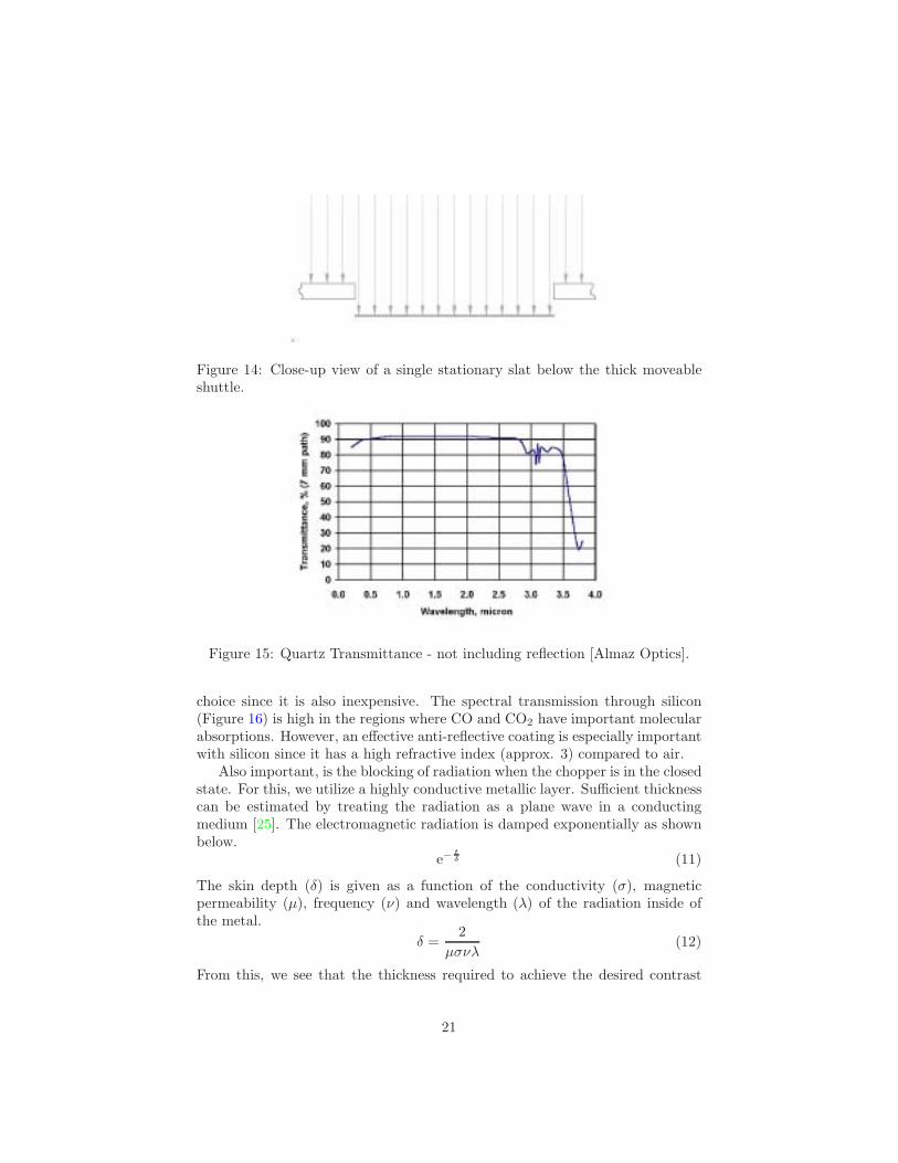
Figure 14: Close-up view of a single stationary slat below the thick moveableshuttle.
Figure 15: Quartz Transmittance - not including reflection [Almaz Optics].
choice since it is also inexpensive. The spectral transmission through silicon(Figure 16) is high in the regions where CO and CO2 have important molecularabsorptions. However, an effective anti-reflective coating is especially importantwith silicon since it has a high refractive index (approx. 3) compared to air.
Also important, is the blocking of radiation when the chopper is in the closedstate. For this, we utilize a highly conductive metallic layer. Sufficient thicknesscan be estimated by treating the radiation as a plane wave in a conductingmedium [25]. The electromagnetic radiation is damped exponentially as shownbelow.
e−tδ (11)
The skin depth (δ) is given as a function of the conductivity (σ), magneticpermeability (µ), frequency (ν) and wavelength (λ) of the radiation inside ofthe metal.
δ =2
µσνλ(12)
From this, we see that the thickness required to achieve the desired contrast
21
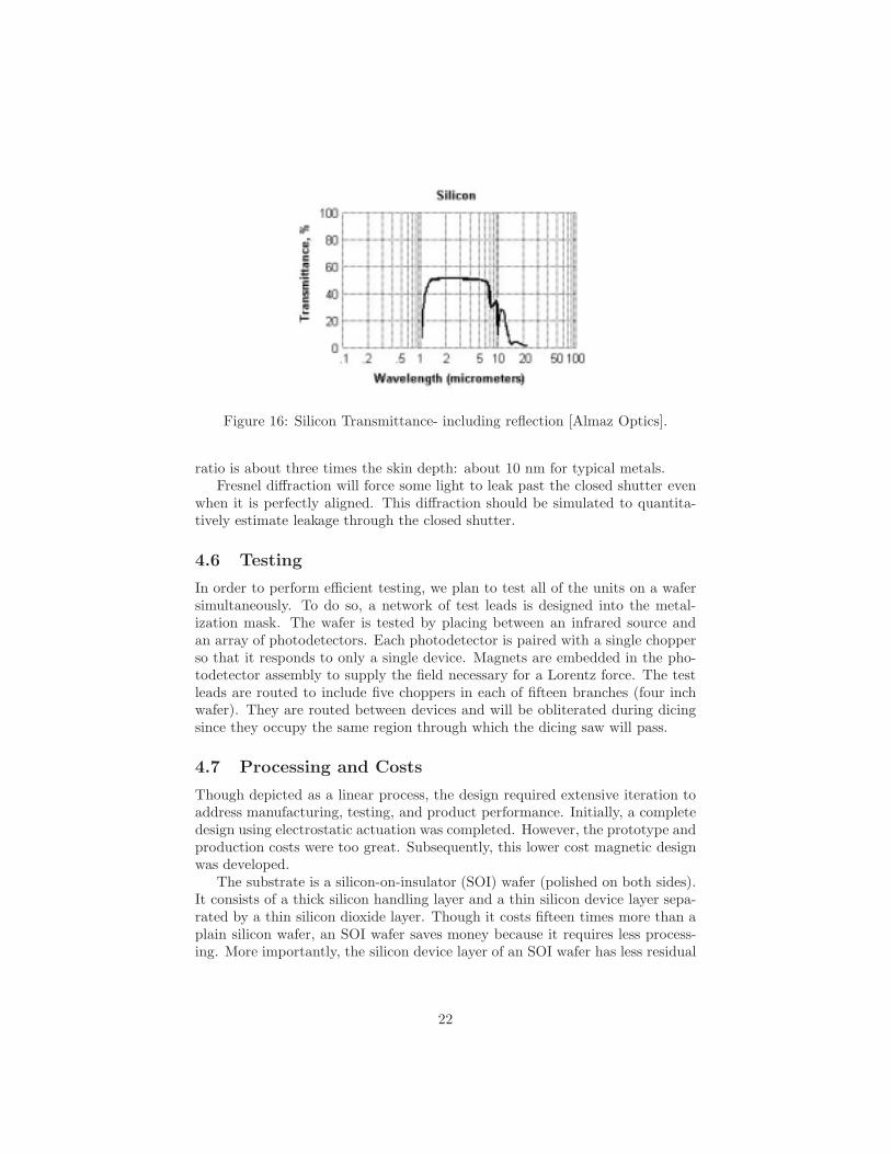
Figure 16: Silicon Transmittance- including reflection [Almaz Optics].
ratio is about three times the skin depth: about 10 nm for typical metals.Fresnel diffraction will force some light to leak past the closed shutter even
when it is perfectly aligned. This diffraction should be simulated to quantita-tively estimate leakage through the closed shutter.
4.6 Testing
In order to perform efficient testing, we plan to test all of the units on a wafersimultaneously. To do so, a network of test leads is designed into the metal-ization mask. The wafer is tested by placing between an infrared source andan array of photodetectors. Each photodetector is paired with a single chopperso that it responds to only a single device. Magnets are embedded in the pho-todetector assembly to supply the field necessary for a Lorentz force. The testleads are routed to include five choppers in each of fifteen branches (four inchwafer). They are routed between devices and will be obliterated during dicingsince they occupy the same region through which the dicing saw will pass.
4.7 Processing and Costs
Though depicted as a linear process, the design required extensive iteration toaddress manufacturing, testing, and product performance. Initially, a completedesign using electrostatic actuation was completed. However, the prototype andproduction costs were too great. Subsequently, this lower cost magnetic designwas developed.
The substrate is a silicon-on-insulator (SOI) wafer (polished on both sides).It consists of a thick silicon handling layer and a thin silicon device layer sepa-rated by a thin silicon dioxide layer. Though it costs fifteen times more than aplain silicon wafer, an SOI wafer saves money because it requires less process-ing. More importantly, the silicon device layer of an SOI wafer has less residual
22
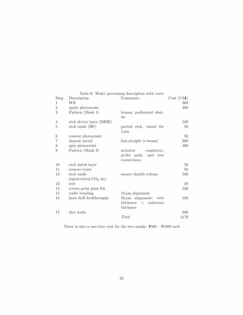
Table 6: Wafer processing description with costsStep Description Comments Cost (US)1 SOI 3002 apply photoresist 4003 Pattern (Mask 1) beams, perforated shut-
tle4 etch device layer (DRIE) 5005 etch oxide (HF) partial etch, timed for
2µm50
6 remove photoresist 507 deposit metal line-of-sight (e-beam) 3008 spin photoresist 4009 Pattern (Mask 2) actuator conductor,
probe pads, and testconnections
10 etch metal layer 5011 remove resist 5012 etch oxide
supercritical CO2 dryensure shuttle release 500
13 test 5014 screen print glass frit 52015 wafer bonding 10µm alignment16 laser-drill feedthroughs 50µm alignment; web
thickness > substratethickness
100
17 dice wafer 200Total 3470
There is also a one-time cost for the two masks: 500 – 1000 each
23

stress than a thermally grown layer. The lower residual stress will decrease therisk that the moving shuttle might bend out of plane and contact the package.
Processing begins by patterning and etching the silicon device layer to forma slotted and moveable shutter along with attached elastic beams (Fig. 17).The underlying oxide is then partially etched to make way for the metallizationthat follows. The metallization layer can then reach both the silicon device layerand the silicon handling layer beneath it. This scheme self-aligns the slats onthe lower silicon layer so that little radiation can pass through the device inits normally closed position. A line-of-sight technique, such as electron beamdeposition, is required to form a truly complementary set of slats on the handlinglayer. From this metallization we also form the Lorentz conductor, the bondingpads, and network of test leads. At this point, all of the features are defined,but the the shuttle is still locked in place by what remains of the oxide layer.
When the beams are finally released, care must be taken to ensure that theydo not become stuck to the substrate by capillary action. The critical stickinglength (LCS) [26], was calculated using the surface tension (γ) for water andalcohol (assuming worst case contact angles θ1 and θ2).
LCS > 1.059
8Eg2h3
γ (cos θ1 + cos θ2)
14
(13)
The beams greatly exceed the critical length for both of these cleaning solvents.While the viscosity of CO2 gas is unknown, supercritical CO2 drying is routinelyused to release parts and we specify its use here.
In order to seal the devices from moisture and particulates, we encapsulatedthem by bonding a plain silicon wafer (polished on both sides) to the finisheddevice wafer. Glass-frit bonding is used because it can be performed at tem-peratures low enough to spare the metallization layer. The glass frit is thick(approx. 50µm) compared to the metal traces and so easily seals over any oftheir steps. The technique begins by screen-printing the bond pattern onto oneof the wafers. They are then aligned within a typical tolerance of less than10µm and then pressed together to form a hermetic seal.
Before separating the dies, holes are laser-drilled through the bonding padsto make way for vertical feedthroughs. Sufficient space is allotted between diesto accommodate the relatively thick (300µm) saw blade that is required to dicea bonded wafer. The holes are positioned to ensure that the web thickness isgreater than the wafer thickness. Figure 18 shows the layout of sixty devices ona 4 inch wafer. The center device is omitted to to make room for a testing pad.All of the wafer processing steps are shown in Table 6; prices are based on theMEMS-Exchange [27].
In order to adapt to the existing spectrometer, each die must be attachedto a mounting plate (Figure 19). Electrical connection is made to the die usinga sub-assembly (not shown) with pins that mate to holes that were previouslydrilled into it. Solder is drawn, through capillary action, into the holes and downto the vertically exposed edges of the bonding pads. Finally, the magnets are fitinto the subassembly, which is then inserted into the housing and secured with
24

Figure 17: Manufacturing Process.
25

Figure 18: A 4 inch wafer holds a maximum of 61 devices.
Table 7: Bill of materials with estimated cost.
Quantity Part Cost (US)1 die (assuming 80% yield) 781 housing 111 subassembly (contains connector
and recess to hold magnets)9
2 magnet (rare earth) 21 labor: assembly 10
Total 110
26

Figure 19: This mounting plate provides a way to insert the chopper into theexisting spectrometer.
a spring clip. Bent pins run out of the sub-assembly through a radial channelto form an external connector. The housing bolts directly into the existingspectrometer (Figure 3). The bill of materials for the complete assembly isshown in Table 7.
5 Modelling
5.1 Layout
The chopper is composed of four mechanically independent shutters. They aredriven by a single conductor that wraps around the periphery of the device.Notice that there is a margin between the actuator beam and the slats to makeroom for the small magnet that will be positioned over the actuator (Figure 20).
Masks are typically drawn within layout software such as that made byCoventor or Mentor Graphics. Here, we use Coventorware, but instead of draw-ing the masks on-screen, scripts were used to generate them (A.3). While thisis more difficult initially, it pays off quickly because one can adjust parameterswith little effort.
5.2 Mechanical
Mechanical simulations were carried out using ANSYS finite element software.Scripts, with parameters identical to those in the Coventor scripts were used togenerate the geometry for the finite element model.
Symmetry was used so that only one half of one of the shutters needed tobe modeled. Along the vertical symmetry plane, all elements were constrained
27

Figure 20: Schematic chopper layout: four mechanically independent shuttersare driven by a single conductor.
from moving normal to it. The ends of the beams were fully constrained asintended in the design. The finite element mesh was refined until the deflectionconverged upon a stable value. Since the magnetic force is distributed across theentire beam, it is modeled as a uniform line pressure. The resulting deflectionwas used to calculate the beam stiffness.
5.3 Dynamic
A modal analysis was run on the same model to find the frequency and modeshape of the first two oscillating modes (Figure 21). The natural frequency ofthe first mode is at approximately 500 Hz. The second mode, which we wish toavoid, is safely positioned at a frequency that is nearly sixty times higher thanthat of the first mode.
A harmonic analysis was set up to plot the displacement as a function offrequency. However, no meaningful results, beyond the locations of the firsttwo resonant frequencies, were generated because no specific damping for ourmodel was included. However, it may be worthwhile to complete this beforeprototypes are made.
5.4 Modelling Recap
The table below (Table 8) summarizes the analyses and simulations that werecarried out to ensure that the device will meet the specifications.
28

Table 8: Simulation SummarySpecs Units Results Simulation and Estimation Methods
Spectral Range 2–5 µm · published material propertiesAperture size >0.5 cm · design inputTransmission >30 % · slot area and reflection estimatesContrast Ratio >50:1 · qualitative argumentOperating Frequency >100 Hz <500 · analytical estimate
· modal simulation (ANSYS)· harmonic simulation (ANSYS)
Operating Temp, Max. >200 C · resistance of all materials· estimated joule heating
Vibration resistance >1 G2 · Hz−1 · analytical calculation based on stiffnessVoltage <15 V 3 · design inputCurrent <20 mA 10 · design inputPower <100 mW 20 · design inputPrototype cost <10,000 US 4,970 · layout simulation (Coventor)
· pricing (MEMS Exchange)Unit cost <200 US 80 · bill of materialsSize of optical head <10x10x5 mm 10x10x5 · design constraint
29

(a) undeformed (b) first mode (c) second mode
Figure 21: The chopper and simulations of its operating modes.
6 Summary
We have designed an infrared chopper to improve infrared spectroscopic com-position measurements on the exhaust from internal combustion engines. Thedevice utilizes a magnetic actuator to drive moveable slats that block infraredradiation. Manufacturing and testing were considered early in the design processto limit costs and increase reliability. Analyses and simulations were performedto show evidence that the design will meet the specifications. Where applicable,recommendations have been made for future work.
7 Acknowledgements
I would like to thank Gideon Eden and Andrew Reading of Sensors Inc. Dr.Reading generously invited me to speak with his staff and Dr. Eden helped meto select a project and settle on specifications. Joe Giachino, at the University ofMichigan, asked many thoughtful questions that encouraged me to think morebroadly about manufacturing issues. His input significantly improved the finaldesign.
A Layout Definition
The layout is defined with two files. The first specifies the process used to makethe device. It is written with internal commands from CoventorWare softwareand must be placed in the design directory. It uses the file extension proc.
The other file defines the geometry. It is written in the TCL scripting lan-guage, which is understood by CoventorWare, and is input using the TCL com-mand source magChopper_coventor.tcl in the terminal window.
30
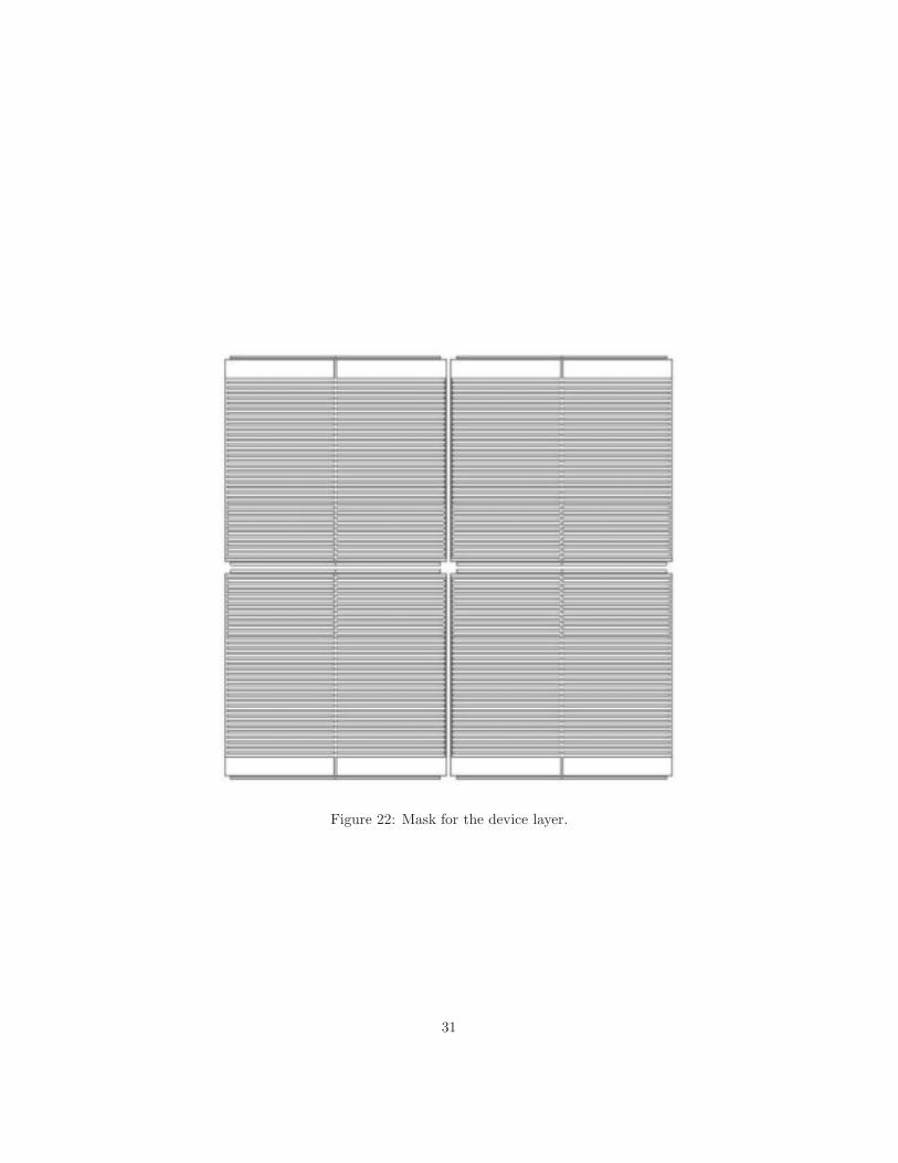
Figure 22: Mask for the device layer.
31

A.1 Individual Masks
A.2 Process Definition File
ProcessVersion=Version=AutoBuilder 2.0
ProcessUnit=
Unit=micronsWafer=
WaferID=w1Mask=GNDLayerName=lyrSOI_subSiMaterial=SILICONThickness=50.0Color=rgb-128-128-128Comment=
Deposit=
WaferID=w1DepositType=PlanarLayerName=lyrSOI_OxideMaterial=OXIDEFace=TOPThickness=1.0Scf=1.0Color=rgb-255-255-255Comment=
Deposit=
WaferID=w1DepositType=PlanarLayerName=lyrSOI_deviceSiMaterial=SILICONFace=TOPThickness=5.0Scf=1.0Color=rgb-128-128-128Comment=
Etch=
WaferID=w1Mask=mskDeviceEtchType=FrontLastLayerEtchUntil=
32

Face=TOPDepth=1.0Color=rgb-0-255-0SidewallAngle=0.0Offset=0.0Polarity=-Comment=
SacrificialEtch=
Material=OXIDEComment=
Deposit=
WaferID=w1DepositType=StackedLayerName=lyrMetalMaterial=ALUMINUMFace=TOPThickness=0.2Scf=1.0Color=rgb-255-200-0Comment=
Etch=
WaferID=w1Mask=mskMetalEtchType=FrontLastLayerEtchUntil=Face=TOPDepth=0.2Color=rgb-0-0-255SidewallAngle=0.0Offset=0.0Polarity=+Comment=
A.3 Mask Generating Script
cellcreate quarter_shutter
#Define geometryset Lb 4000 ;#beam lengthset Ls 4200 ;#shuttle lengthset y_max 4000 ;#shuttle widthset w 12 ;#beam width
33

set d 50 ;#maximum deflectionset u 30 ;#shutter frame widthset v 20 ;#shutter push-spar half-widthset f 10 ;#minimum shutter side clearanceset c_na 60 ;#end clearance (non-actuated end)set c_act 300 ;#minimum end clearance (actuated end)
# shutter clearance is determined differently depending# on whether the beam or the shutter is longerif $Lb/2 > [expr $Ls/2+$f] set x_max [expr $Lb/2]
else set x_max [expr $Ls/2 + $f]
# Determine number of slots that will fit within shuttleset S_slots [expr $y_max-2*$d-2*$w-$c_na-$c_act]set j 0while [expr (2*$j+1)*$d] < $S_slots incr j 1
set nSlats [expr $j-1]
# draw slotsfor set k 0 $k < $nSlats incr k set x1 $vset x2 [expr $Ls/2-$u]set y1 [expr $w + $c_na + (2*$k+2)*$d]set y2 [expr $w + $c_na + (2*$k+3)*$d]cat:rectangle -layer mskDevice $x1 $y1 $x2 $y2
# Draw cut to free lower beamset x1 0set x2 [expr $Lb/2]set y1 0set y2 $dcat:rectangle -layer mskDevice $x1 $y1 $x2 $y2
# Draw cuts to free shuttleset x1 $vset x2 $x_maxset y1 [expr $d+$w]set y2 [expr $d+$w+$c_na ]cat:rectangle -layer mskDevice $x1 $y1 $x2 $y2
34

set x1 $x_maxset x2 [expr $Ls/2]set y1 [expr $d+$w+$c_na ]set y2 [expr $w + $c_na + (2*$nSlats+1)*$d +$d]cat:rectangle -layer mskDevice $x1 $y1 $x2 $y2
set x1 $vset x2 $x_maxset y1 [expr $w + $c_na + (2*$nSlats+1)*$d +$d ]set y2 [expr $y_max-($d+$w)]cat:rectangle -layer mskDevice $x1 $y1 $x2 $y2
# Draw cut to free upper beamset x1 0set x2 [expr $Lb/2]set y1 [expr $y_max-$d]set y2 $y_maxcat:rectangle -layer mskDevice $x1 $y1 $x2 $y2
select -allboolean -op orviewfit
# cellsave
# make copies to create full unitcellcreate shutterreference -name "quarter_shutter" 0.0 0.0reference -name "quarter_shutter" -reflect on 0.0 0.0reference -name "quarter_shutter" -angle 180.0 0.0 0.0reference -name "quarter_shutter" -angle 180.0 -reflect on 0.0 0.0
cellsaveviewfit
B Finite Element Script
All mechanical simulations were run using the ANSYS parametric design lan-guage (APDL). The simulation can be launched by typing /INPUT, magChopper_ansys.apdl.If you wish to rerun with different parameters simply type FINISH then /CLEand issue the input command again.
/prep7
!Define geometryLb=4000e-6 !beam lengthLs=4000e-6 !shuttle length
35

y_max=4000e-6 !shuttle widthw=12e-6 !beam widthd=50e-6 !maximum deflectionu=30e-6 !shutter frame widthv=20e-6 !shutter push-spar half-widthf=10e-6 !minimum shutter side clearancec_na=60e-6 !end clearance (non-actuated end)c_act=300e-6 !minimum end clearance (actuated end)
thickness=5e-6et, 1, plane2 ! was shell43keyopt,1,3,3r, 1, thickness !assign thickness
!shutter clearance is determined differently depending!on whether the beam or the shutter is longer*IF,(Lb/2),GT,(Ls/2+f), THENx_max=Lb/2
*ELSEx_max=Ls/2 + f
*ENDIF
!Determine number of slots that will fit within shuttleS_slots=y_max-2*d-2*w-c_na-c_actnMax=9999999*do,j,1,nMaxj=j+1*if,(2*j+1)*d,GT,S_slots,thennSlats=j-1*exit
*endif*enddo
!Draw wafer from which material is then etchedrectng, 0, x_max, 0, y_max
!Draw cuts to create slots (rectng x1, x2, y1, y2)*do,k,1,nSlatsrectng, v, Ls/2-u, w + c_na + (2*k)*d, w + c_na + (2*k+1)*dasba, 1, 2 !subtract etched areanumcmp,AREA !keeps IdNumber of resultant area fixed at one
*enddo
!Draw cut to free lower beamrectng, 0, Lb/2, 0, dasba, 1, 2
36
numcmp,AREA!Draw cuts to free shuttlerectng, v, x_max, d+w, d+w+c_naasba, 1, 2numcmp,AREArectng, x_max, Ls/2, d+w+c_na, w + c_na + (2*nSlats+1)*d +dasba, 1, 2numcmp,AREArectng, v, x_max, w + c_na + (2*nSlats+1)*d +d, y_max-(d+w)asba, 1, 2numcmp,AREA!Draw cut to free upper beamrectng, 0, Lb/2, y_max-d, y_maxasba, 1, 2numcmp,AREA
!Define Material PropertiesYoungsModulus = 190e9PoissonRatio = 0.23Density = 2330mp, ex, 1, YoungsModulusmp, prxy, 1, PoissonRatiomp, dens, 1, Density
!MeshingnDiv = 10 !size = 10e-6esize,,nDivtriangular=0dimension2D=’2D’mshape,triangular,dimension2DSMRTSIZE,1amesh, all
!Boundary Conditions!fixed BCs on ends of beamsnsel, s, loc, y, y_max-(d+w), y_maxnsel, a, loc, y, 0, d+wnsel, r, loc, x, Lb/2, x_maxAllSelected=’ALL’AllDOF=’ALL’d, AllSelected, AllDOF
!symmetry BCsnsel,s, loc, x, 0d, AllSelected, UX
!d, AllSelected, ROTZ
37

FINISH
SolutionType = ’Modal’
/SOLU !Analysis Type and Options
!Distribute load along actuator beamnsel, s, loc, y, y_max-dnsel, r, loc, x, 0, Ls/2AppliedLoad = -80e-6 / 2*get, nCoincNodes, node,, countAllSelected=’ALL’F, AllSelected, Fy, AppliedLoad/nCoincNodes
*IF, SolutionType , EQ, ’Static’, THENANTYPE, STATIC
*ELSEIF, SolutionType , EQ, ’Modal’, THENANTYPE, MODALMODOPT,SUBSP,2MXPAND,2
*ELSEIF, SolutionType , EQ, ’Harmonic’, THENANTYPE,HARMICHROPT,FULL ! Full harmonic responseHROUT,OFF ! Print results as amplitudes and phase anglesOUTPR,BASIC,1NSUBST,30 ! 30 Intervals within freq. rangeHARFRQ,1000,4000 ! Frequency range (could intu)
*ENDIF
NSEL, ALLSOLVE
FINISH
!Post-Processing*IF, SolutionType , EQ, ’Static’, THEN/POST1!symmetry expansion > reflection across plane!normal to x axis (i.e., the yz plane)/EXPAND,2,RECT,half,1e-12PLDISP,0!PLNSOL,S,EQV,0,1!PLNSOL,U,Y,0,1
38

*ELSEIF, SolutionType , EQ, ’Modal’, THEN/POST1/EXPAND,2,RECT,half,1e-12SET,FIRSTPLDISP !Display first mode shape!ANMODE,10,0.5, ,0 ! Animate mode shape
*ELSEIF, SolutionType , EQ, ’Harmonic’, THEN! graph the response/POST26nNode=3135NSOL,2,nNode,U,Y,3135UY ! Store UX Displacements/GRID,1! Turn grid on/AXLAB,Y,DISP! Y-axis label disp!/GROPT,LOGX,ON !graph frequency on log axisPLVAR,2 ! Display variables 2 and 3
*ENDIF
References
[1] Spears, M., “On-Vehicle Emissions Measurements and Test Procedures,”International Conference on Future Worldwide Emission Requirements forPassenger Cars and Light Duty Vehicles; Milan, Italy; December 11, 2003,http://www.sensors-inc.com/press.htm; accessed March 28,2005.
[2] Klingenberg , H., “Automobile Exhaust Testing,” Springer-Verlag, Berlin,1996, p. 143.
[3] E.L. Tury, K. Kaste, R.E. Johnson, and D.O. Danielson “U.S. patent#5,060,505,” 1991
[4] Sensors Inc., “SEMTECH-G,” Sensors Inc., Saline, Michigan.,http://www.sensors-inc.com/semtechg.htm; accessed March 28, 2005.
[5] K. T. Ulrich and S. D. Eppinger, Product Design and Development,McGraw-Hill, 2000.
[6] Boston Electronics Corporation “360C OEM Ultraminiature Optical Chop-per Brochure,” Brookline, MA.
[7] Hinds Instruments Inc., “PEM-90 Photoelastic Modulator SystemsBrochure,” Hillsboro, OR.
[8] Peter Krippner, Jurgen Mohr, and Volker Sai1e “ElectromagneticallyDriven Microchopper for Integration into Microspectrometers Based on the
39

LIGA Technology,” SPIE Conference on Miniaturized Systems with Micro-Optics and MEMS, Santa Clara, CA, September 1999 SPIE Vol. 3878, p144.
[9] Obermeier, E., J. Lin, and V. Schlichting “Electrostatically ActivatedMicro-Shutter in (110) Silicon,” Micromechanical Systems, DSC-Vol. 40,ASME 1992.
[10] Li, M.J.;, I. S.Aslam, S.I.; Ewin, A.; Fettig, R.K.; Franz, D. ; Kotecki,C. , Kutyrev, A.S.; Moseley, S.H.; Monroy, C ; Mott, D.B.; Zheng, Y.“Fabrication of Microshutter Arrays for Space Application,” SPIE meetingon Microelectronic and MEMS Technologies, Edinburgh, United Kingdom,May/June 2001.
[11] David Dausch and Scott Goodwin-Johansson “Electrostatic MEMS Chop-per for Uncooled IR Detectors,” Infrared Technology and ApplicationsXXVIII, Bjorn F. Andresen, Gabor F. Fulop, Marija Strojnik, Editors,Proceedings of SPIE Vol. 4820 (2003) pg. 261.
[12] M. J. Li, A. Bier, R. K. Fettig, D. Franz, R. Hu, T. King, A. S. Ku-tyrev, B. A. Lynch, S. H. Moseley, D. B. Mott, D. Rapchun, R.F. Silver-berg, W. Smith, L. Wang, Yun Zheng C. Zinke, “Microshutter Arrays forNear-Infrared Applications on the James Webb Space Telescope,” MEMSComponents and Applications for Industry,Automobiles, Aerospace, andCommunication II, Siegfried W. Janson, Editor, Proceedings of SPIE Vol.4981 (2003), p. 113.
[13] Ching, Michael T.; Brennen, Reid A.; White, Richard M. “Microfabricatedoptical chopper,” Proceedings of SPIE - The International Society forOptical Engineering, v 1992, 1993, p 40-46 Conference: Miniature andMicro-Optics and Micromechanics, Jul 14-15 1993, San Diego, CA, USA.
[14] Sugiyama, S.; Tabata, O.; Shimaoka, K.; Asahi, R., “Micromachined sen-sors using polysilicon sacrificial layer etching technology,” Technical Di-gest., International Electron Devices Meeting, 11-14 Dec. 1994, 127-130.
[15] Benecke, W. and Riethmuller, W. “Applications of silicon microactuatorsbased on bimorph structures,” IEEE MEMS Workshop (Salt Lake City,Utah.1989) (New York IEEE) pp 116-20.
[16] H. Guckel, J. Klein, T. Christenson, K. Skrobis, M. Laudon, and E. Lovell“Thermo-magnetic metal flexure actuators,” Proc. IEEE Solid State Sen-sors and Actuators Workshops (Hilton Head’92), June 1992, pp. 73-75.
[17] Gianchandani, Y. “Electrothermal Microactuators for Long Throw andHigh Force,” ERC Seminar, University of Michigan, Ann Arbor, MI, March13, 2001.
[18] C. Niezrecki et al., “Piezoelectric actuation: state of the Art,” The Shockand Vibration Digest, vol. 33(4), pp 269-280, 2001.
40

[19] Roark, R. Roark’s Formulas for Stress and Strain, p. 104, case 2d, 6thed.,(New York: McGraw-Hill, 1989)
[20] Xia Zhang and W.C. Tang “Viscous air damping in laterally driven mi-croresonators,” Proceedings of the IEEE Workshop on Micro Electro Me-chanical Systems, 1994, MEMS ’94, p.199.
[21] W. Ye, X. Wang, W. Hemmert, D. Freeman, and J. White, “Air Dampingin Laterally Oscillating Microresonators: A Numerical and ExperimentalStudy,” Journal of Microelectromechanical Systems, Vol. 12, No. 5, October2003, p.557.
[22] C. Kittel and H.Kroemer, Thermal Physics, 2nd ed., (W. H. Freeman, NY,1980), pg. 403.
[23] P Bahukudumbi and Ali Beskok “A phenomenological lubrication modelfor the entire Knudsen regime,” J. Micromech. Microeng. 13 (November2003) 873-884.
[24] Paul Klocek, Handbook of Infrared Optical Materials, Marcel Dekker(1991).
[25] R. K. Wangsness, Electromagnetic Fields, p. 384, (John Wiley and Sons,NY 1986).
[26] R. Legtenberg, J. Elders and M. Elwenspoek, “Stiction of Surface Micro-machined Structures after Rinsing and Drying: Model and Investigationof Adhesion Mechanisms,” Transducers ’93, Yokohama, Japan, June 7-10,1993, p198-201.
[27] Mems Exchange http://mems-exchange.org; accessed March 28, 2005.
41