
Microfluidic Fiber Lasers - Research Laboratory of Electronics
12
Chapter 31. Microfluidic Fiber Lasers 31-1 Microfluidic Fiber Lasers Academic and Research Staff Alexander Stolyarov, Ofer Shapira, Nicholas D. Orf, John D. Joannopoulos, and Yoel Fink Sponsor: NSF/MRSEC, US Army Microfluidic dye lasers (MDL) have recently emerged as promising candidates to facilitate the fusion of optics and fluidics at the microscale. Their primary advantage over gas or solid state lasers is the inherent wavelength tunabililty which can be achieved by changing the type of dye used, the dye concentration, or the host solution. Here, we report on the design and characterization of a MDL with a fundamentally new characteristic, one that couples the fluid mechanics property of the gain medium with its optical properties, namely, surface tension enabled laser cavity tunability. This laser cavity is composed of a liquid dye-doped plug positioned inside a hollow core photonic bandgap fiber, with its surface contours and surrounding cylindrical solid cladding defining the cavity geometry. With this geometry, we demonstrate two unique laser features: 1) linear motion of a lasing source that emits light radially from a fiber and 2) modulation of the laser threshold by fluid mechanical deformation of the laser cavity. The radially emitting microfluidic fiber laser we developed is shown schematically in the figure below. It consists of a hollow core photonic bandgap fiber with a R590-doped water plug positioned in the otherwise hollow or silicone oil filled core. Pump light from a second harmonic of an Nd: YAG laser is delivered along the fiber axis to the fluidic plug. The multilayer Bragg reflecting structure that runs along the entire length of the fiber serves two purposes. The reflections at glancing incidence guide the 532nm pump light axially to the gain medium, while the red-shifted normal incidence reflections provides the confinement of radially oscillating laser modes originating from the fluorescing dye-doped water.
Transcript of Microfluidic Fiber Lasers - Research Laboratory of Electronics
Chapter 31. Microfluidic Fiber Lasers
31-1
Microfluidic Fiber Lasers Academic and Research Staff Alexander Stolyarov, Ofer Shapira, Nicholas D. Orf, John D. Joannopoulos, and Yoel Fink Sponsor: NSF/MRSEC, US Army Microfluidic dye lasers (MDL) have recently emerged as promising candidates to facilitate the fusion of optics and fluidics at the microscale. Their primary advantage over gas or solid state lasers is the inherent wavelength tunabililty which can be achieved by changing the type of dye used, the dye concentration, or the host solution. Here, we report on the design and characterization of a MDL with a fundamentally new characteristic, one that couples the fluid mechanics property of the gain medium with its optical properties, namely, surface tension enabled laser cavity tunability. This laser cavity is composed of a liquid dye-doped plug positioned inside a hollow core photonic bandgap fiber, with its surface contours and surrounding cylindrical solid cladding defining the cavity geometry. With this geometry, we demonstrate two unique laser features: 1) linear motion of a lasing source that emits light radially from a fiber and 2) modulation of the laser threshold by fluid mechanical deformation of the laser cavity. The radially emitting microfluidic fiber laser we developed is shown schematically in the figure below. It consists of a hollow core photonic bandgap fiber with a R590-doped water plug positioned in the otherwise hollow or silicone oil filled core. Pump light from a second harmonic of an Nd: YAG laser is delivered along the fiber axis to the fluidic plug. The multilayer Bragg reflecting structure that runs along the entire length of the fiber serves two purposes. The reflections at glancing incidence guide the 532nm pump light axially to the gain medium, while the red-shifted normal incidence reflections provides the confinement of radially oscillating laser modes originating from the fluorescing dye-doped water.

Chapter 31. Microfluidic Fiber Lasers
31-2 RLE Progress Report 150
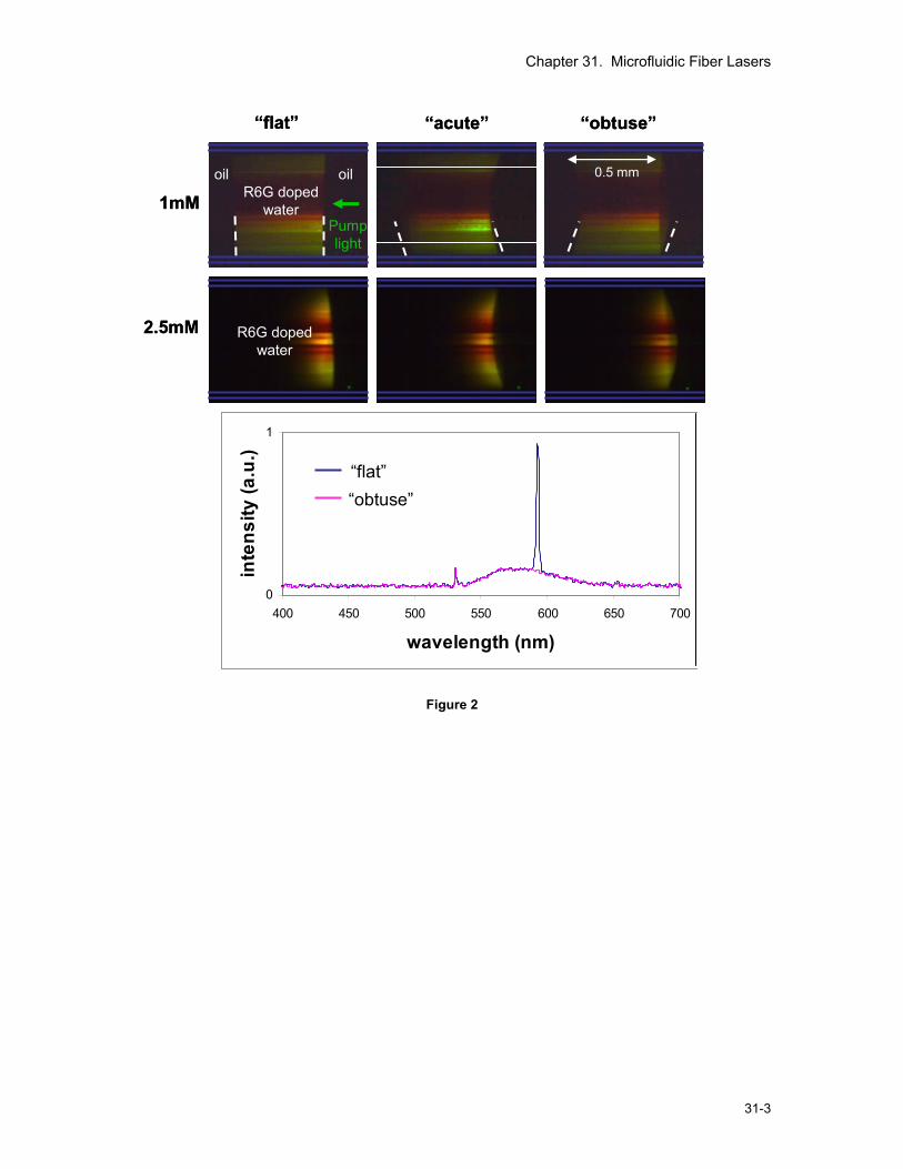
Figure 1: The images at the bottom of the figure captures three instances of a moving R6G-doped water doped water plug, lasing radially from inside a hollow core photonic bandgap fiber. Also visible is the higher frequency green pump light, which is incident from the left. (The RLE logo in the background measures ~7 cm left to right and the fiber is positioned ~ 7 cm in front of the logo.) An interesting feature of this laser that emerges as a consequence of coupling fluid mechanics with optics is the ability to tune the laser threshold by controlling the meniscus shape at the water/oil interface. We have shown that in maintaining the same pump beam energy, the fiber laser can be switched between on and off states by adding curvature to the meniscus. These results are depicted in the figure below in which we see a lower threshold for the concave meniscus as compared to both the convex and flat menisci. Pumping the gain medium at an energy which slightly exceeds the threshold of the convex/flat meniscus case leads to the spectrum marked “flat” in the figure. Changing the curvature to be concave leads to the spectrum marked “obtuse”, in which we observe the lasing peak disappear. Such drastic changes in the lasing spectrum which occur from changes in the meniscus shape, could pave the way for novel fiber and fluidic based pressure sensors.
Custom made hermetic optical
coupler
oil
Pump Light
Radially EmittedLaser Light from
R6G-doped water plug Microfluidic control system
Vacuum reservoir
High pressure reservoir
Electronically controlled microdispensing valves
(z1, t1) (z2, t2)
Multilayer structureCladding
H 2 O
Custom made hermetic optical
coupler
oil
Pump Light
Radially EmittedLaser Light from
R6G-doped water plug Microfluidic control system
Vacuum reservoir
High pressure reservoir
Electronically controlled microdispensing valves
(z1, t1) (z2, t2)
Multilayer structureCladding
H 2 O
Chapter 31. Microfluidic Fiber Lasers
31-3
Pump light
R6G doped water
oiloil 0.5 mm
1mM
2.5mM
“flat” “acute” “obtuse”
0
1
400 450 500 550 600 650 700
wavelength (nm)
inte
nsity
(a.u
.)
R6G doped water
“flat”“obtuse”
Pump light
R6G doped water
oiloil 0.5 mm
1mM
2.5mM
“flat” “acute” “obtuse”
0
1
400 450 500 550 600 650 700
wavelength (nm)
inte
nsity
(a.u
.)
R6G doped water
“flat”“obtuse”
Figure 2
Chapter 31. Microfluidic Fiber Lasers
31-4 RLE Progress Report 150
INTEGRATED THIN-FILMS FIBER DEVICES AND LENSLESS IMAGING ARRAYS Academic and Research Staff Fabien Sorin, Ayman F. Abouraddy, Ofer Shapira, Matthew Spencer, Sylvain Danto, Nick Orf, John D. Joannopoulos, and Yoel Fink This work was supported in part by US DOE, NSF/MRSEC and the ISN.
The development of semiconductors technology has been for the most part the result of the reduction of device feature size, enabled by continuous improvements in thin film processing. Achieving smaller sizes not only enables an increase in the device packing density, but is also crucial for the functionality, efficiency and design of complex devices. Multimaterial integrated fiber devices produced by simple and inexpensive fiber drawing techniques and recently proven to exhibit many of the semiconductor devices functionalities, follow the same trend. We recently demonstrated that the reduction of cross sectional sizes and the design and controlled processing of a thin film structure inside fiber devices significantly increase their performance [1]. This study had significant practical implications in the optimal design of photodetecting fibers to be used in applications such as remote sensing, large-area optical-detection array systems, and functional fabrics. In this project, we study how this new thin-film design can be used to increase the device density integrated in a single fiber, and demonstrate the significant impact this has on developing complex functionalities inside fiber devices. Especially, we build a more sensitive single grid lensless imaging system compared to the one previously reported [2].
In previous publications [1-3], we have insisted on the fiber extension along one dimension that brings significant practical advantages, besides their low cost and ease of production. We are however yet to investigate the use and resources of the angular and radial dimensions of the fiber devices. In this project, we build complex thin-film structures inside a fiber to enable the extraction of angular and spectral information. Figure 1 shows how angular discrimination is obtained while Figure 2 explains the principle behind wavelength discrimination. Finally, we build a fiber grid made out of these new fibers which enables significant improvements to the lens less imaging system previously reported as shown on Figure 3.
[1] Fabien Sorin, Ayman F. Abouraddy, Nick Orf, Ofer Shapira, Jeff Viens, Jeremy Arnold, John D. Joannopoulos and Yoel Fink, “Multimaterial Photodetecting Fibers: a Geometric and Structural Study”, Advanced Materials 19: 3872 (2007). [2] A. F. Abouraddy, O. Shapira, M. Bayindir, J. Arnold, F. Sorin, D. Saygin-Hinczewski, J. D. Joannopoulos, Y. Fink, “Large-scale optical-field measurements with geometric fiber constructs” Naure Materials 5, 532 (2006). [3] M. Bayindir, F. Sorin, A. F. Abouraddy, J. Viens, S. D. Hart, J. D. Joannopoulos, Y. Fink, “Metal-Insulator-Semiconductor Optoelectronic Fiber” Nature 431, 826 (2004).

Chapter 31. Microfluidic Fiber Lasers
31-5
Figure 1: Our approach to have angular discrimination is to treat each quadrant as an independent detector by applying a voltage only between two adjacent electrodes at a time as depicted on the 2 schematics with connections in red or blue of Figure 1 (A1). On the schematics where the applied potential is represented in red, the electric field in quadrant 1 is stronger than in the three other quadrants. When light is incident with a zero angle, most of the photons are absorbed in 1 which generates a higher current than when light is incident at ±180o for which the photons are absorbed in the low electric field region (quadrants 2, 3 and 4). This gives rise to the angular dependence of the photo-current apparent on Figure 1 (A2): Similar approach is used on Figure 1 B but with two thin films where the electrodes have been rotated by 45 degrees. Angular discrimination down to 4 degrees have been obtained using this technique.

Chapter 31. Microfluidic Fiber Lasers
31-6 RLE Progress Report 150
Figure 2: Light impingent on a fiber device is also characterized, besides its direction, by a frequency, and a photon flux. What influences the photo-current is the total number of photons absorbed which depends on their frequency, through the penetration depth of the photdetecting material, the film thickness and the number of photons reaching the film. when a monochromatic beam reaches the fiber, the two unknowns, the frequency ω and Nph can not be determined by a single photo-current measurement.The integration of a second film inside the fiber device as depicted on Figure 3A has the significant advantage to solve this problem and to bring spectral resolution to the fiber. Indeed, the ratio of the measured currents in the inner layer to the current in the outer layer turns out to be a function of ω only, independent of Np.
On Figure 2, A is the SEM pictures of the whole cross section of a fiber with two thin films. Below: magnification on two electrodes and on an electrode contacting a thin film. B: Dependence of the r function on wavelength for two fibers with the same glass thickness (t = 100nm) but different glass compositions. C: Dependence of the r function on wavelength for two fibers with the same glass As40Se54Te6 and different film thicknesses (t = 100nm and t = 200nm). D: Ratio of currents for different relative powers for an illumination at two wavelengths, 488 nm and 830 nm.

Chapter 31. Microfluidic Fiber Lasers
31-7
Figure 3: The lens-less imaging system described on [2] required the intensity distribution measurements on two solid-core fibers based grids placed on parallel planes in the near and far fields. Using the phase retrieval algorithm we were able to reconstruct the intensity distribution at the plane of the object. We present here an alternative strategy where we demonstrate the use of a single array, capable of the same imaging functionality, with the same filling factor, but made out of dual-ring fiber components. At the heart of this new approach is the capability to obtain two diffracted patterns as in [2] of the same object, but this time on a same plan for two different laser beams illuminating the object at the same time as depicted on Figure 3. Since, as we explained above on Figure 2, we can separate the contribution of each wavelength with dual-ring fibers, a single grid captures two patterns of the object illuminated by two different wavelengths enabling the reconstruction of the object autocorrelation function. Initial results are presented here: better image quality are expected in the near future.

Chapter 31. Microfluidic Fiber Lasers
31-8 RLE Progress Report 150
In-Fiber Semiconductor Filament Arrays
Academic and Research Staff Daosheng Deng, Nick D. Orf, A. M. Stolyarov, Dr. Ayman F. Abouraddy, Professor John D. Joannopoulos, Professor Howard A. Stone, and Professor Yoel Fink Sponsors ISN, MRSEC A new class of fibers incorporating multiple materials thermally drawn from a macroscopic preform has recently studied by our group [1]. In contrast with conventional fibers, which consist of a single insulating material typically silica with the possible addition of air cavities these new fibers combine insulators, semiconductors and metals in prescribed gemoetries. The semiconductor film geometry is important in structures such as cylindrical multilayer photonic bandgap fibers and sensitive optical and thermal fiber detectors. The purpose of this study is to examine the geometric evolution of fluid films of semiconductor materials during the thermal fiber draw down process. We observe that under certain conditions a cylindrically symmetric thin sheet spontaneously evolves into a periodic array of filaments when the sheet thickness reaches a critical length scale. Interestingly, in contrast to other related phenomena, the axial dimension remains continuous. A controlled and reproducible approach of thermal drawing processing is developed allowing us to follow the fleeting evolution of fluid breakup in a frozen solid state, resulting in potentially unprecedented extended semiconductor nanofilaments. The underlying mechanism driving the layer-to-filament evolution is a capillary-flow instability mechanism determined by materials viscosity. By dissolving the polymer matrix, centimetre-long semiconductor filaments of aspect ratio 106 are extracted. This work provides a simple methodology for producing well-ordered filament arrays with nanometre-scale cross-sectional dimensions and extended lengths. References [1] A.F. Abouraddy, M. Bayindir, G. Benoit, S.D. Hart, K. Kuriki, N. Orf, O. Shapira, F. Sorin, B. Temelkuran, Y. Fink, “Towards multimaterial multifunctional fibres that see, hear, sense and communicate” Nature Materials 6, 336-347 (2007). [2] D. S. Deng, N. D. Orf, A. F. Abouraddy, A. M. Stolyarov, J. D. Joannopoulos, H. A. Stone, and Y. Fink, “In-Fiber semiconductor filament arrays”, Nano Letters, forthcoming.

Chapter 31. Microfluidic Fiber Lasers
31-9
Breakup of layers at the nanometer scale. (a) Sketch of the preform with multiple films of decreasing thickness and fiber cross-section indicating breakup of thinner layers. (b) An SEM micrograph of whole cross-sectional view of fiber; inset showing that average spacing of break-up segments varies linearly with the final layer thickness. (c) Magnification Se/PSU fiber cross-section (boxed area in b) (the final layer thicknesses in fiber are 700, 96, 65, and 17 nm, respectively) showing that the layers are broken when pulled to below 100 nm thickness; inset for a further magnified section of the 17 nm layer. (d) Magnification As2Se3/PES fiber cross-section (the final layer thicknesses in fiber are 270, 70, 14, and 3 nm, respectively) showing that the layers are maintained to sub-15 nm thickness; inset shows a further magnified section of the 3 nm layer.

Chapter 31. Microfluidic Fiber Lasers
31-10 RLE Progress Report 150
Thermally-induced crystalline domains growth within multimaterial FET fiber devices Academic and research staff Sylvain Danto, Fabien Sorin, Zheng Wang, Matthew Spencer, Nicholas D. Orf, John D. Joannopoulos, Yoel Fink Sponsor DARPA, ISN, DOE, NSF The fabrication process of light-weight, flexible and cheap multimaterial fibres has been recently demonstrated and complex devices, integrating insulators, conductors and amorphous semiconductors, are now designed with a large number of functionalities [1-3]. However, the elaboration of metal-insulator-semiconductor fiber structures is basically confined to amorphous semiconductors, exhibiting inferior electronic transport properties due to disorder and the associated electronic confinement. Here, for the first time, we demonstrate that the judicious combination of a thermal drawing with a simple and inexpensive post-drawing annealing treatment can be extended to incorporate crystalline semiconductors into micro-structured multi-material fibers. With this controlled growth of crystalline domains in the semiconductor, active electric devices in a single multi-material fiber may be constructed. Flexible field-effect p-channel fiber transistors of meters length are drawn. To demonstrate the post-drawing thermal crystallization scheme, we fabricate fiber constituted of a solid-core chalcogenide glass, of composition As40Se52Te8 (Tg = 165 °C), in intimate contact with four Sn electrodes that extend the full length of the fibre and surrounded with a High-Tg polymeric PES cladding (Fig. 1). The resulting meters-long fiber is cut into several pieces of equal length and diameter, each piece being subsequently annealed at 208 °C for a given period of time, between 0 and 24 days. As the phase transition of the semiconductor from amorphous to crystals occurs, we observe a drop of the electrical resistance by six orders of magnitude (Fig. 1). According to SEM micrographs observations of fibre cross-sections, we show that heterogeneous crystallization initiates at the surface of the As40Se52Te8 solid-core glass. After around 6 days of annealing a low electrical resistance surface channel of crystalline material connects the tin electrodes. Then, crystalline domains gradually extend through the bulk, reducing the electrical resistance even further. Post-drawing crystallization of the embedded glass drastically reduces the density of localized states inside the band-gap of the semiconductor and hence increases carrier mobility. As a concrete application, we demonstrate a single-fiber p-channel field-effect transistor with a source-to-drain conductance controlled by an applied gate voltage. We adopted a thin-film transistor layout, using the p-type As40Se52Te8 as the channel (Fig. 2). The crystallized thin-film channel is contacted by two parallel Sn electrodes as the source and the drain. The gate electrode consists of a partially crystallized As40Se52Te8 solid-core contacted by a Sn electrode and a PES shell serves as the gate dielectric. The carrier concentration in the semiconductor channel is then modulated by an electric field generated by the applied gate voltage. SEM micrographs of the cross-section of such fiber transistors are presented in Fig. 2A. This transistor structure is assembled in a millimeter-scale preform, and is subsequently drawn down to a micron-scale fiber while preserving the relative dimension and location of all structural features in the cross-section. A fiber transistor, designed to turn-on under accumulation conditions, was prepared and annealed at 208 °C for 24 days. As can be seen in Fig. 2B, after annealing, the source-to-drain current ∆IDS shows a strongly nonlinear dependence on the applied gate voltage VG under a VDS of 10 V and a gate voltage swept from -300 V to +300 V in 120 s. As a comparison, without annealing, identical fiber structure yields extremely low channel conductivity and no dependence on the gate voltage. To the best of our knowledge, this result represents, for the first time, a field-effect transistor observed in a meter-long single-fiber device fabricated by simple thermal drawing technique. It paves the way to embed high-quality metal-insulator-crystalline semiconductor structures into unprecedented fiber lengths, enabling electronic junction in flexible polymer fibers and fabrics.

Chapter 31. Microfluidic Fiber Lasers
31-11
Figure 1 Time-evolution of the electrical resistance of fiber annealed at 208 °C for 24 days. All the measurements are made between two adjacent Sn electrodes (lFib. = 15 cm, ΦFib. = 1.30 mm) at room temperature. As the crystallinity increases, the electrical resistance drops by six orders of magnitude. SEM micrographs of the fiber cros-section show the growth of crystalline domains, which initiate at the surface of the As40Se52Te8 solid-core glass and then gradually propagate through the bulk.

Chapter 31. Microfluidic Fiber Lasers
31-12 RLE Progress Report 150
D S
G
G
D S
Semiconductor channel
B
0-300 100-100 200-200 300
0
1
2
3
4
Unannealed
208 °C / 288 hrs
Gate voltage (V)
∆I D
S(μ
A)
A
SDG
Amorphous As40Se52Te8
Sn
PES
Crystalline As40Se52Te8
D S
G
G
D S
G
D S
Semiconductor channel
B
0-300 100-100 200-200 300
0
1
2
3
4
Unannealed
208 °C / 288 hrs
Gate voltage (V)
∆I D
S(μ
A)
0-300 100-100 200-200 300
0
1
2
3
4
Unannealed
208 °C / 288 hrs
UnannealedUnannealed
208 °C / 288 hrs208 °C / 288 hrs
Gate voltage (V)
∆I D
S(μ
A)
A
SDG
Amorphous As40Se52Te8
Sn
PES
Crystalline As40Se52Te8
Amorphous As40Se52Te8
Sn
PES
Crystalline As40Se52Te8
Figure 2 p-channel field-effect transistor fiber device (A) SEM micrographs of the cross-section of the fiber device (G: Gate, D: Drain, S: Source) (A Bottom) Whole structure (A Top) Magnification of the device. The gate electrode is engineered to be the As40Se52Te8 solid-core of the fiber. Two parallel source and drain electrodes are in contact with a semiconducting As40Se52Te8 film, surrounding the gate but separated from it by an insulating PES polymer shell (B) Change of drain-to-source current ∆IDS as a function of the gate voltage VG for unannealed (gray) and 24 days annealed fibers (red). The gate voltage is applied with a period of 120 s, VDS = 10 V. The annealed fiber clearly shows a DC field-effect. References [1] Bayindir M., Sorin F., Abouraddy A.F., Viens J., Hart S.D., Joannopoulos J.D., Fink Y., “Metal-Insulator-Semiconducting optoelectronics fibres” Nature 431, 826-829 (2004). [2] Abouraddy A.F., Shapira O., Bayindir M., Arnold J., Sorin F., Saygin-Hinczewski D., Joannopoulos J.D., Fink Y., “Large-scale optical-field measurements with geometric fibre constructs” Nature Materials 5, 532-536 (2006). [3] Bayindir M., Shapira O., Saygin-Hinczewski D., Viens J., Abouraddy A.F., Joannopoulos J.D., Fink Y., “Integrated fibres for self-monitored optical transport” Nature Materials 4, 820-824 (2005).


![Tunable Erbium-Doped Fiber Lasers Using Various Inline Fiber … · 2016-02-18 · erbium-doped fiber lasers [4], distributed feedback fiber lasers [5], and Brillouin erbium-doped](https://static.fdocuments.net/doc/165x107/5f5d6d92d306cb22521e3c0b/tunable-erbium-doped-fiber-lasers-using-various-inline-fiber-2016-02-18-erbium-doped.jpg)