microelectronics presentation on semiconductor devices and circuit theory
59
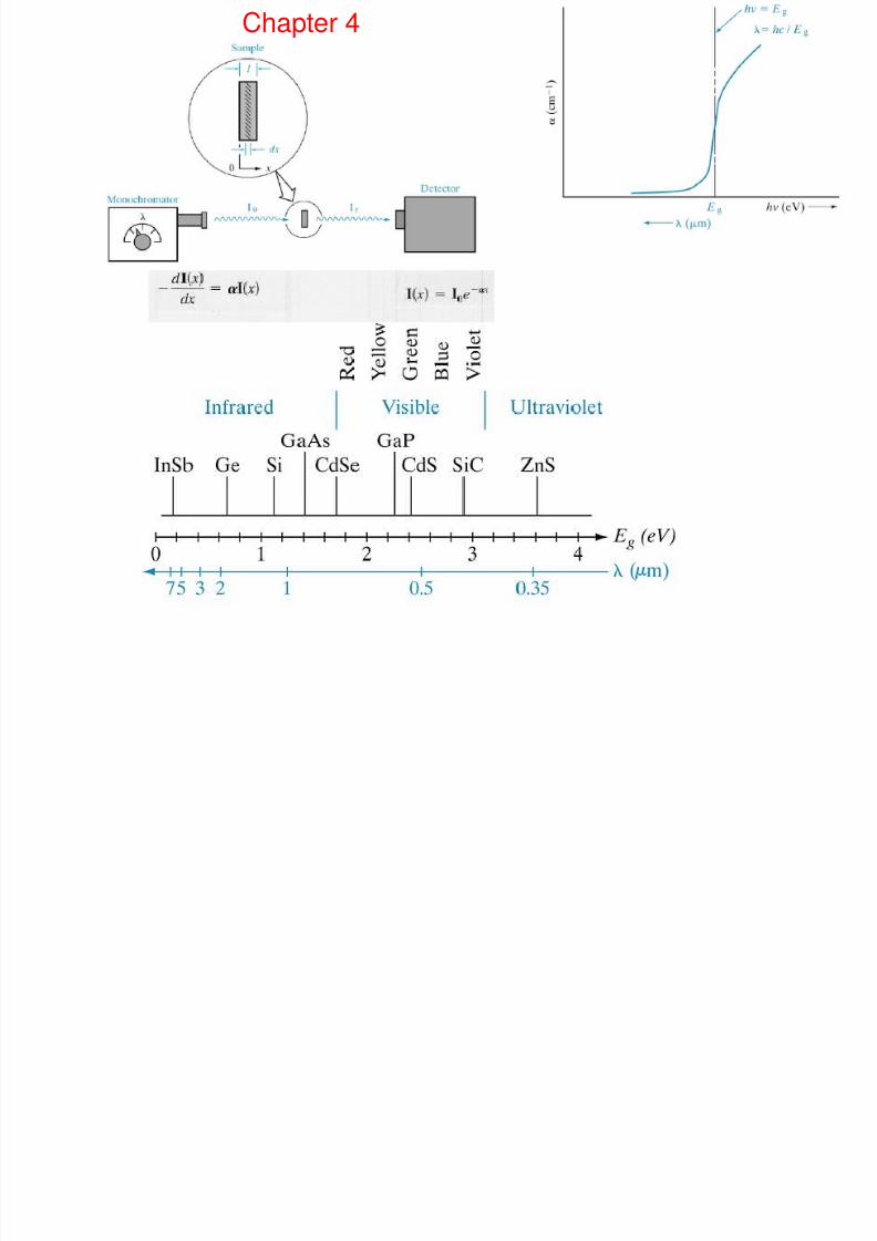
Ch a p t e r 4
-
Upload
ashutosh-kumar -
Category
Documents
-
view
241 -
download
0
Transcript of microelectronics presentation on semiconductor devices and circuit theory
8/19/2019 microelectronics presentation on semiconductor devices and circuit theory
http://slidepdf.com/reader/full/microelectronics-presentation-on-semiconductor-devices-and-circuit-theory 1/59
Chapter 4

8/19/2019 microelectronics presentation on semiconductor devices and circuit theory
http://slidepdf.com/reader/full/microelectronics-presentation-on-semiconductor-devices-and-circuit-theory 2/59
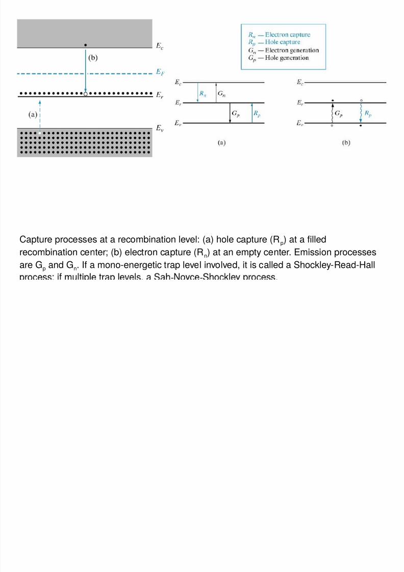
Excitation and recombination mechanisms in
photoluminescence with a trapping level for electrons.
8/19/2019 microelectronics presentation on semiconductor devices and circuit theory
http://slidepdf.com/reader/full/microelectronics-presentation-on-semiconductor-devices-and-circuit-theory 3/59
Capture processes at a recombination level: (a) hole capture (Rp) at a filled
recombination center; (b) electron capture (Rn) at an empty center. Emission processes
are Gp and Gn. If a mono-energetic trap level involved, it is called a Shockley-Read-Hall
- -

8/19/2019 microelectronics presentation on semiconductor devices and circuit theory
http://slidepdf.com/reader/full/microelectronics-presentation-on-semiconductor-devices-and-circuit-theory 4/59

8/19/2019 microelectronics presentation on semiconductor devices and circuit theory
http://slidepdf.com/reader/full/microelectronics-presentation-on-semiconductor-devices-and-circuit-theory 5/59
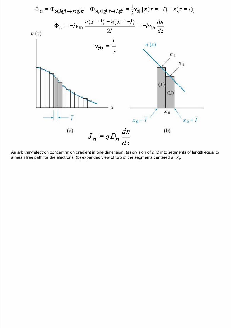
Spreading of a pulse of electrons by diffusion
8/19/2019 microelectronics presentation on semiconductor devices and circuit theory
http://slidepdf.com/reader/full/microelectronics-presentation-on-semiconductor-devices-and-circuit-theory 6/59
An arbitrary electron concentration gradient in one dimension: (a) division of n( x ) into segments of length equal to
a mean free path for the electrons (b) expanded view of two of the segments centered at x !.
8/19/2019 microelectronics presentation on semiconductor devices and circuit theory
http://slidepdf.com/reader/full/microelectronics-presentation-on-semiconductor-devices-and-circuit-theory 7/59
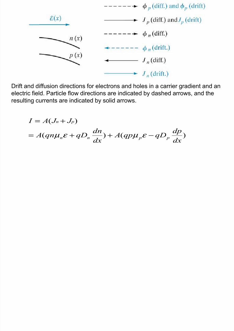
"rift and diffusion directions for electrons and holes in a carrier gradient and an
electric field. #article flow directions are indicated by dashed arrows$ and the
resulting currents are indicated by solid arrows.
)()(
)(
dx
dpqDqp A
dx
dnqDqn A
J J A I
p pnn
pn
−++=
+=
ε µ ε µ
8/19/2019 microelectronics presentation on semiconductor devices and circuit theory
http://slidepdf.com/reader/full/microelectronics-presentation-on-semiconductor-devices-and-circuit-theory 8/59
8/19/2019 microelectronics presentation on semiconductor devices and circuit theory
http://slidepdf.com/reader/full/microelectronics-presentation-on-semiconductor-devices-and-circuit-theory 9/59
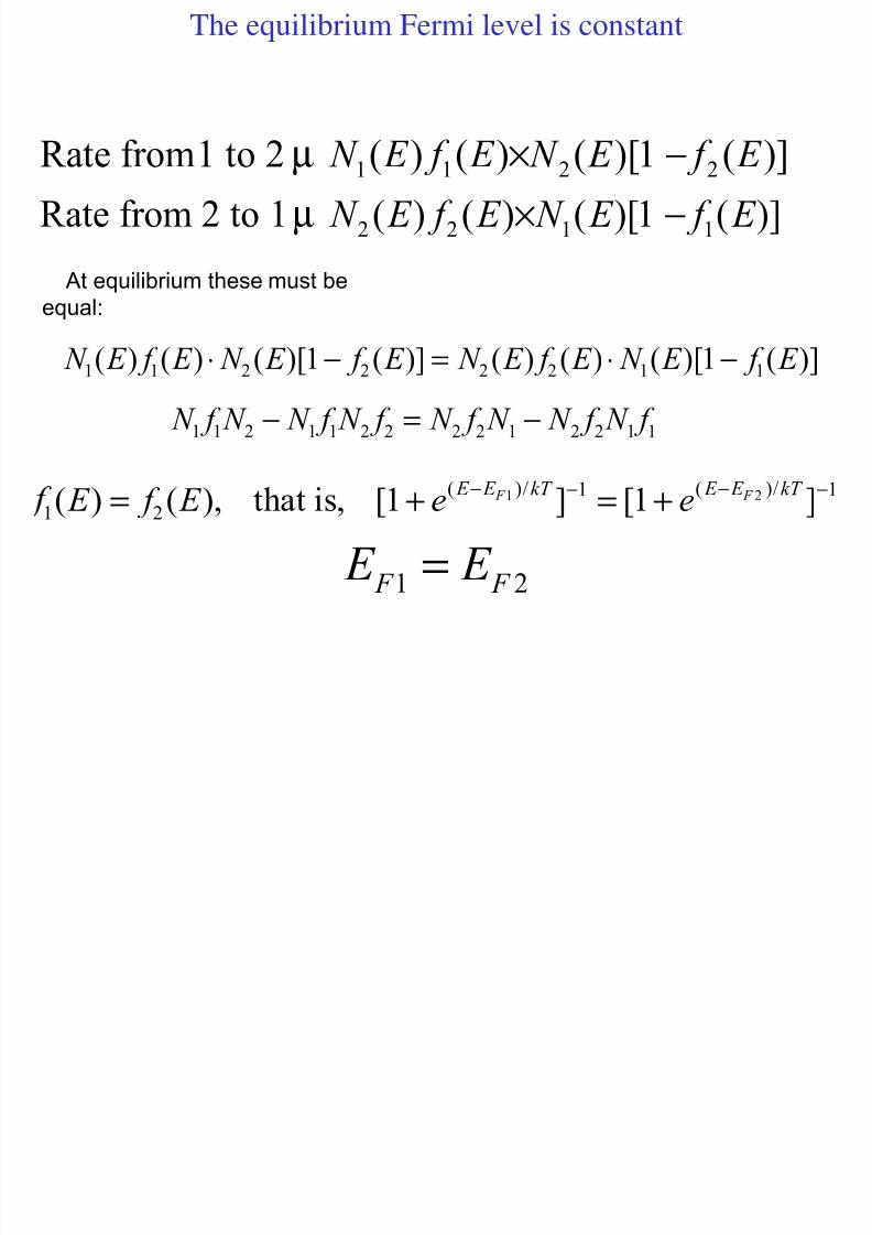
1 1 2 2Rate from1 to 2 ( ) ( ) ( )[1 ( )] N E f E N E f E µ × −
2 2 1 1Rate from 2 to 1 ( ) ( ) ( )[1 ( )] N E f E N E f E µ × −
At equilibrium these must beequal:
N E f E N E f E N E f E N E f E 1 1 2 2 2 2 1 11 1( ) ( ) ( )[ ( )] ( ) ( ) ( )[ ( )]⋅ − = ⋅ −
N f N N f N f N f N N f N f 1 1 2 1 1 2 2 2 2 1 2 2 1 1− = −
E f E e e E E kT E E kT F F
1 2
1 11 11 2( ) ( ), [ ] [ ]( )/ ( )/= + = +− − − − that is,
1 2 F F E E =
The equilibrium Fermi level is constant
8/19/2019 microelectronics presentation on semiconductor devices and circuit theory
http://slidepdf.com/reader/full/microelectronics-presentation-on-semiconductor-devices-and-circuit-theory 10/59
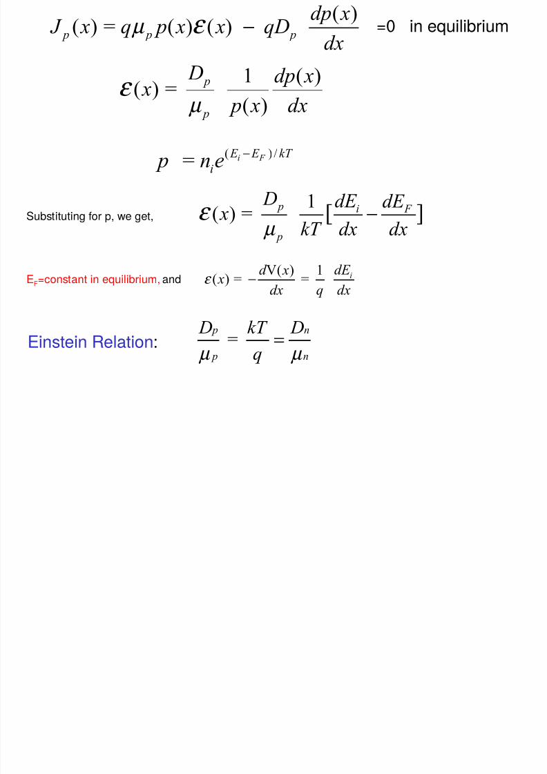
( )( ) = ( ) ( ) p p p
dp x J x q p x x qD
dx µ ε −
= p n
p n
D kT D
q µ µ
=
( ) / = i F E E kT
i p n e−
=0 in equilibrium
V( ) 1( ) = = idE d x x
dx q dxε −
1 ( ) ( ) = ( )
p
p
D dp x x p x dx µ ε
1 ( ) = [ ] p i F
p
D dE dE x
kT dx dx µ ε −Substituting for p, we get,
Einstein Relation:
EF=constant in equilibrium, and

8/19/2019 microelectronics presentation on semiconductor devices and circuit theory
http://slidepdf.com/reader/full/microelectronics-presentation-on-semiconductor-devices-and-circuit-theory 11/59
The mobility and diffusivity arerelated because drift velocity issuperimposed on top of random
Brownian motion, which also drivesdiffusion.
kT/q is the thermal voltage = 26meV at 300K.

8/19/2019 microelectronics presentation on semiconductor devices and circuit theory
http://slidepdf.com/reader/full/microelectronics-presentation-on-semiconductor-devices-and-circuit-theory 12/59
0 F i
n i
E E
kT
i
F E
kT
i
n n e
n n e
− ÷
− ÷ ÷
=
⇒ =
( )
0
( )
F i
p i
E E
kT
i
F E
kT
i
p n e
p n e
− − ÷
− − ÷ ÷
=
⇒ =
Majority carrierIMREF changes
little from EF.Minority carrierIMREF changesa lot.
Non Equilibrium
Equilibrium
Equilibrium
Non Equilibrium

8/19/2019 microelectronics presentation on semiconductor devices and circuit theory
http://slidepdf.com/reader/full/microelectronics-presentation-on-semiconductor-devices-and-circuit-theory 13/59

8/19/2019 microelectronics presentation on semiconductor devices and circuit theory
http://slidepdf.com/reader/full/microelectronics-presentation-on-semiconductor-devices-and-circuit-theory 14/59
8/19/2019 microelectronics presentation on semiconductor devices and circuit theory
http://slidepdf.com/reader/full/microelectronics-presentation-on-semiconductor-devices-and-circuit-theory 15/59
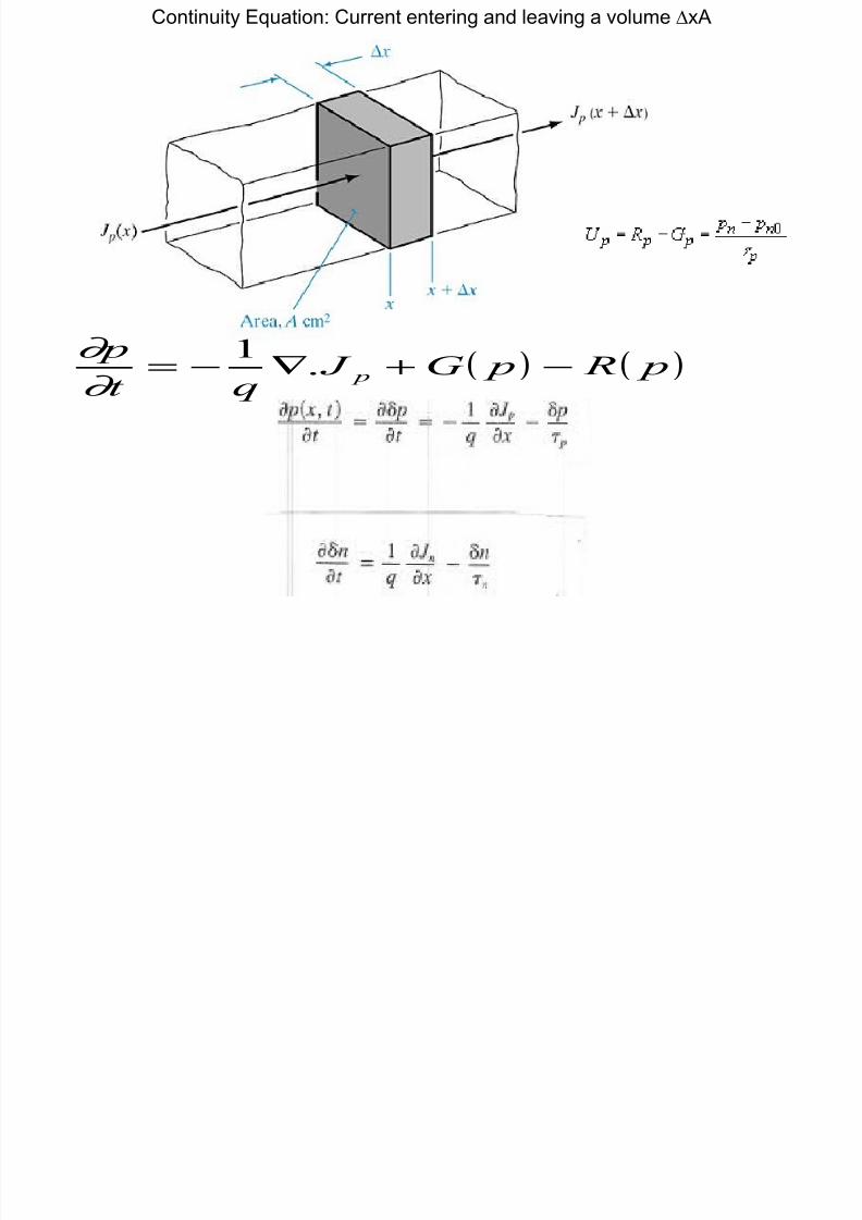
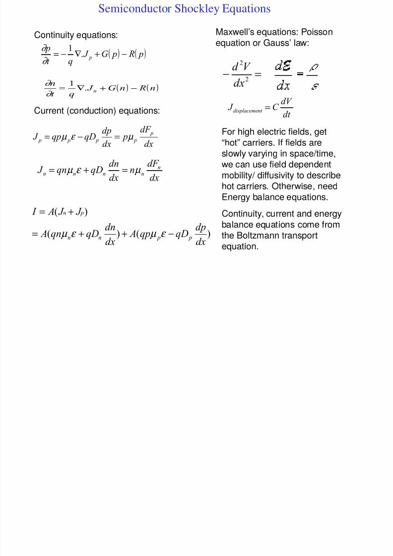
%ontinuity Equation: %urrent entering and leaving a volume &xA
( ) ( ) p R pG J qt
p p −+∇−= .
1
∂
∂
d dift t

8/19/2019 microelectronics presentation on semiconductor devices and circuit theory
http://slidepdf.com/reader/full/microelectronics-presentation-on-semiconductor-devices-and-circuit-theory 16/59
where C2= ∆p
p(x) = p0 + δp (x)
and no drift current
8/19/2019 microelectronics presentation on semiconductor devices and circuit theory
http://slidepdf.com/reader/full/microelectronics-presentation-on-semiconductor-devices-and-circuit-theory 17/59
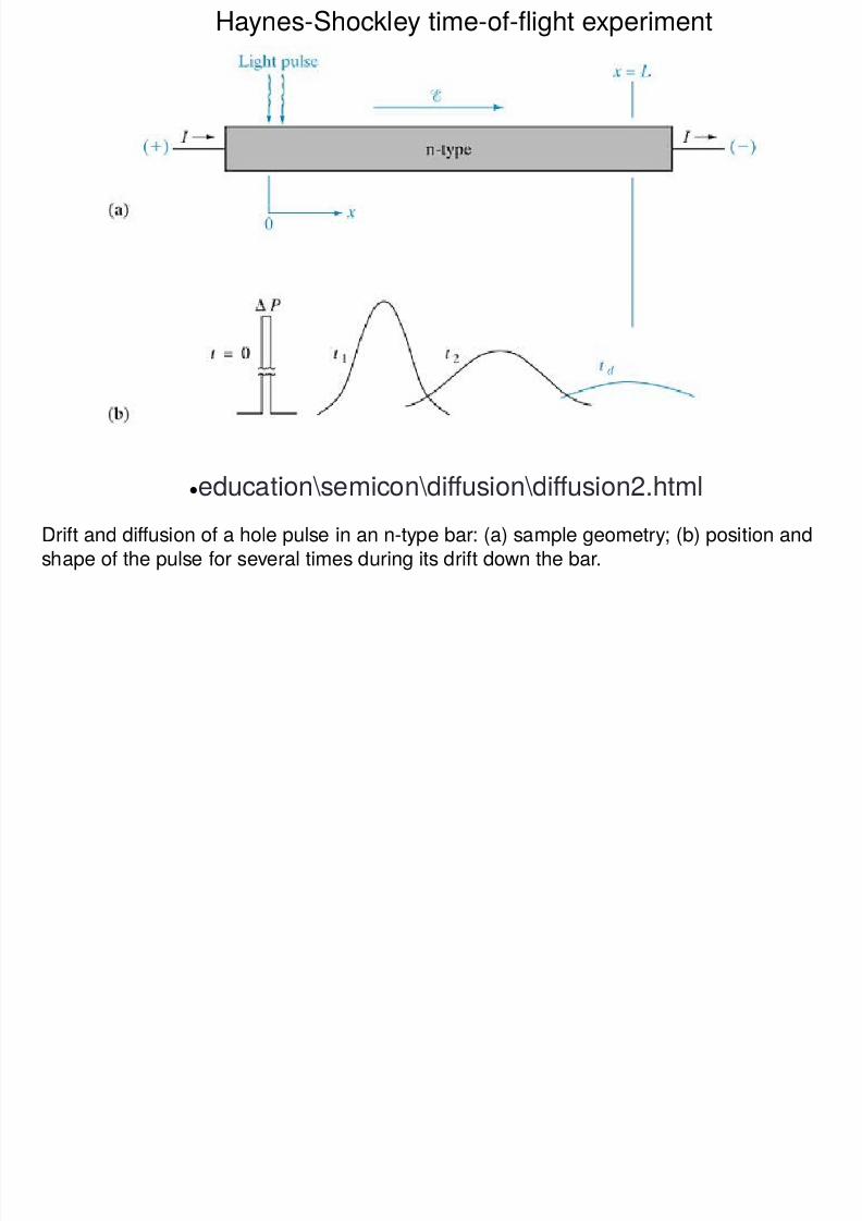
Drift and diffusion of a hole pulse in an n-type bar: (a) sample geometry; (b) position and
shape of the pulse for several times during its drift down the bar.
•education\semicon\diffusion\diffusion2.html
Haynes-Shockley time-of-flight experiment
S i d Sh kl E i
8/19/2019 microelectronics presentation on semiconductor devices and circuit theory
http://slidepdf.com/reader/full/microelectronics-presentation-on-semiconductor-devices-and-circuit-theory 18/59
Semiconductor Shockley Equations
nn n n n
dF dn J qn qD n
dx dx µ ε µ = + =
( ) ( ) p R pG J
qt
p p −+∇−= .
1
∂
∂
)()(
)(
dx
dpqDqp A
dx
dnqDqn A
J J A I
p pnn
pn
−++=
+=
ε µ ε µ
p
p p p p
dF dp J qp qD p
dx dx µ ε µ = − =
( ) ( )n RnG J qt
nn −+∇= .
1
∂
∂
Continuity equations:
Current (conduction) equations:
Maxwell’s equations: Poissonequation or Gauss’ law:
For high electric fields, get“hot” carriers. If fields areslowly varying in space/time,we can use field dependentmobility/ diffusivity to describehot carriers. Otherwise, needEnergy balance equations.
Continuity, current and energybalance equations come fromthe Boltzmann transportequation.
dt
dV C J nt displaceme =
=−2
2
dx
V d
8/19/2019 microelectronics presentation on semiconductor devices and circuit theory
http://slidepdf.com/reader/full/microelectronics-presentation-on-semiconductor-devices-and-circuit-theory 19/59
Ch t 4 SUMMARY

8/19/2019 microelectronics presentation on semiconductor devices and circuit theory
http://slidepdf.com/reader/full/microelectronics-presentation-on-semiconductor-devices-and-circuit-theory 20/59
Chapter 4 SUMMARY
• 1. Excess carriers, above the equilibrium values contributed by doping, may becreated optically (or by electrical biasing in devices). Generation-recombination(G-R) of electron-hole pairs ( EHPs) can occur by absorption of photons with energygreater than the bandgap, balanced by direct or indirect recombination.
• 2. G-R processes can be mediated by traps, especially deep traps near mid-gap.Band-to-band or trap-assisted G-R processes lead to an average lifetime for theexcess carriers. Carrier lifetime multiplied by the optical generation rate, establishesa steady–steady excess population of carriers. The square root of carrier lifetimemultiplied by the diffusion coefficient determines the diffusion length.
• 3. In equilibrium we have a constant Fermi level. In non-equilibrium with excess
carriers, Fermi levels are generalized to separatequasi-Fermi levels
for electronsand holes. The quasi-Fermi level splitting is a measure of the departure fromequilibrium. Minority carrier quasi-Fermi levels change more than majority carrierquasi-Fermi levels because the relative change of minority carriers is larger.Gradients in the quasi-Fermi level determine the net drift-diffusion current.
• 4. Diffusion flux measures the flow of carriers from high to low concentration regions, and is given by the diffusivity times the concentration gradient . The
direction of diffusion current is opposite to the flux for the negative electrons, but inthe same direction for the positive holes. Carrier diffusivity is related to mobility bythe thermal voltage kT/q ( Einstein relation).
• 5. When carriers move in a semiconductor due to drift/diffusion, the time-dependentcarrier concentrations at different points is given by the carrier continuity equationwhich says that if more carriers flow into a point than flow out, the concentration
will increase as a function of time and vice versa. G-R processes also affect carrierconcentrations.
8/19/2019 microelectronics presentation on semiconductor devices and circuit theory
http://slidepdf.com/reader/full/microelectronics-presentation-on-semiconductor-devices-and-circuit-theory 21/59
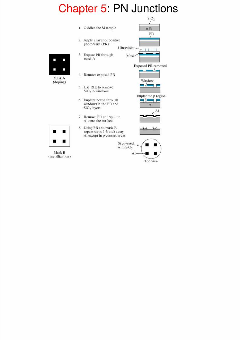
Chapter 5: PN Junctions
Eqilibrimpnjnction

8/19/2019 microelectronics presentation on semiconductor devices and circuit theory
http://slidepdf.com/reader/full/microelectronics-presentation-on-semiconductor-devices-and-circuit-theory 22/59
(a) isolated, neutral regions of p-type and n-type material andenergy bands for the isolatedregions; (b) junction, showingspace charge in the transitionregionW , the resulting electricfield and contact potential V0, and
the separation of the energy
bands; (c) directions of the fourcomponents of particle flow withinthe transition region, and theresulting current directions.
Equilibrium p-n junction

8/19/2019 microelectronics presentation on semiconductor devices and circuit theory
http://slidepdf.com/reader/full/microelectronics-presentation-on-semiconductor-devices-and-circuit-theory 23/59

8/19/2019 microelectronics presentation on semiconductor devices and circuit theory
http://slidepdf.com/reader/full/microelectronics-presentation-on-semiconductor-devices-and-circuit-theory 24/59
Space charge and electric field distribution within the transition region of a p-n junctionwithNd >Na: (a) the transition region, with x = 0 defined at the metallurgical junction; (b)
charge density within the transition region, neglecting the free carriers; (c) the electricfield distribution, where the reference direction is arbitrarily taken as the +x-direction.
=−2
2
dx
V d
education\pn\pnformation3\PNFormation2.htm
education\pn\pnformation2\pnformation2.htm
8/19/2019 microelectronics presentation on semiconductor devices and circuit theory
http://slidepdf.com/reader/full/microelectronics-presentation-on-semiconductor-devices-and-circuit-theory 25/59
V)
8/19/2019 microelectronics presentation on semiconductor devices and circuit theory
http://slidepdf.com/reader/full/microelectronics-presentation-on-semiconductor-devices-and-circuit-theory 26/59

8/19/2019 microelectronics presentation on semiconductor devices and circuit theory
http://slidepdf.com/reader/full/microelectronics-presentation-on-semiconductor-devices-and-circuit-theory 27/59
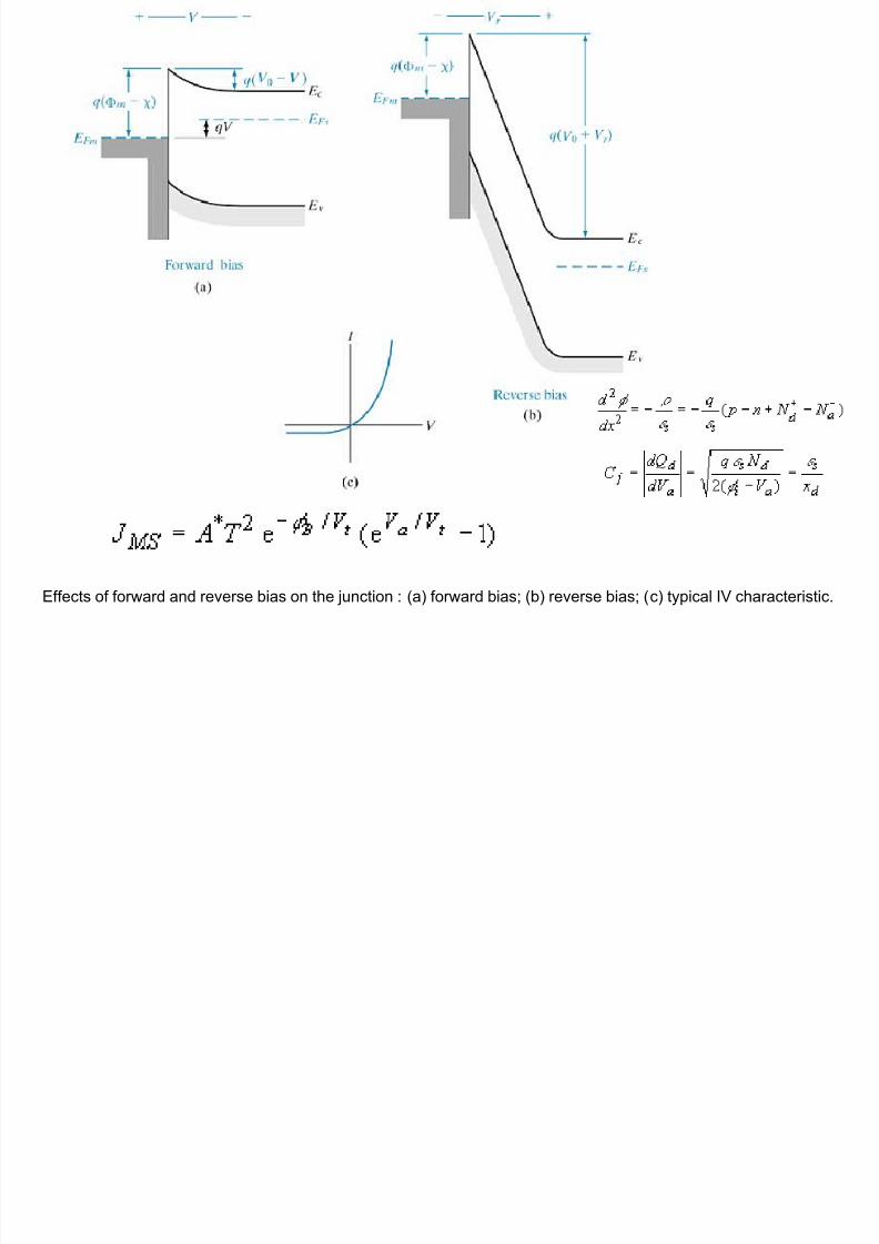
Effects of a bias at a p-n junction;transition region width and electricfield, electrostatic potential, energyband diagram, and particle flow andcurrent directions within W for (a)equilibrium, (b) forward bias, and (c)reverse bias.
The diffusion current changes
exponentially with bias because ofthe exponential Boltzmanndistribution of carrier energies. Theopposing drift current isindependent of bias because here
the current is (minority carrier)supply limited.
education\pn\biasedPN2\BiasedPN2.html
education\pn\biasedPN\BiasedPN.html

8/19/2019 microelectronics presentation on semiconductor devices and circuit theory
http://slidepdf.com/reader/full/microelectronics-presentation-on-semiconductor-devices-and-circuit-theory 28/59
Forward-biased junction
2
( 1)
n
p
xqV LkT
n no no
ino
d
n n
p p p e e
n p
N
n p
− ÷ ÷ ÷ = + −
=
∆ = ∆
8/19/2019 microelectronics presentation on semiconductor devices and circuit theory
http://slidepdf.com/reader/full/microelectronics-presentation-on-semiconductor-devices-and-circuit-theory 29/59
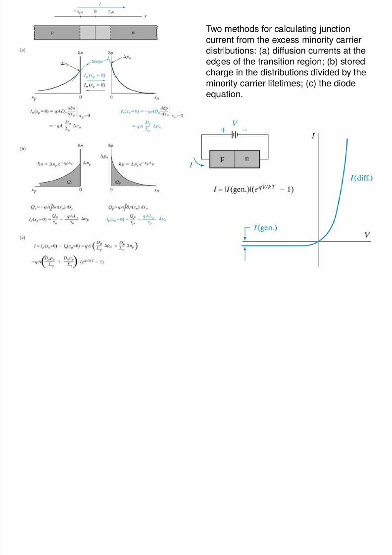
Two methods for calculating junctioncurrent from the excess minority carrierdistributions: (a) diffusion currents at the
edges of the transition region; (b) storedcharge in the distributions divided by theminority carrier lifetimes; (c) the diodeequation.
8/19/2019 microelectronics presentation on semiconductor devices and circuit theory
http://slidepdf.com/reader/full/microelectronics-presentation-on-semiconductor-devices-and-circuit-theory 30/59
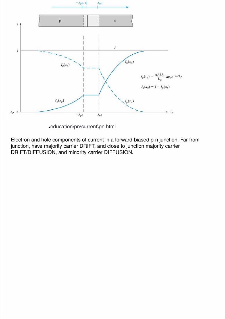
Electron and hole components of current in a forward-biased p-n junction. Far from
junction, have majority carrier DRIFT, and close to junction majority carrierDRIFT/DIFFUSION, and minority carrier DIFFUSION.
•education\pn\current\pn.html
Reversebiasedpnjunction

8/19/2019 microelectronics presentation on semiconductor devices and circuit theory
http://slidepdf.com/reader/full/microelectronics-presentation-on-semiconductor-devices-and-circuit-theory 31/59
(a) Minority carrier distributionsnear the reverse-biased junction; (b) variation of thequasi-Fermi levels. It splitsdue to applied voltage, butopposite to the way forforward bias.
(b) Reverse saturation currentis due to diffusion ofminority carriers to edge of
depletion region, followed bydrift. Current is voltageindependent because itdepends on how oftencarriers are supplied todepletion edge, not how fastthey travel across it.
Reverse-biased p-n junction
Reversebreakdowninapnjunction

8/19/2019 microelectronics presentation on semiconductor devices and circuit theory
http://slidepdf.com/reader/full/microelectronics-presentation-on-semiconductor-devices-and-circuit-theory 32/59
Reverse breakdown in a p-n junction
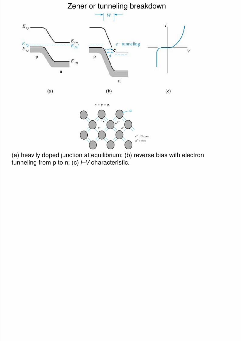
Zenerortunnelingbreakdown
8/19/2019 microelectronics presentation on semiconductor devices and circuit theory
http://slidepdf.com/reader/full/microelectronics-presentation-on-semiconductor-devices-and-circuit-theory 33/59
(a) heavily doped junction at equilibrium; (b) reverse bias with electrontunneling from p to n; (c)I–V characteristic.
Zener or tunneling breakdown
8/19/2019 microelectronics presentation on semiconductor devices and circuit theory
http://slidepdf.com/reader/full/microelectronics-presentation-on-semiconductor-devices-and-circuit-theory 34/59
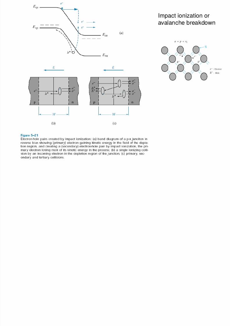
Impact ionization oravalanche breakdown

8/19/2019 microelectronics presentation on semiconductor devices and circuit theory
http://slidepdf.com/reader/full/microelectronics-presentation-on-semiconductor-devices-and-circuit-theory 35/59

8/19/2019 microelectronics presentation on semiconductor devices and circuit theory
http://slidepdf.com/reader/full/microelectronics-presentation-on-semiconductor-devices-and-circuit-theory 36/59
A breakdown or Zener diode: (a)I–V characteristic; (b) application as a voltageregulator. If Vo voltage greater than ~10 V, breakdown due to avalanche.

8/19/2019 microelectronics presentation on semiconductor devices and circuit theory
http://slidepdf.com/reader/full/microelectronics-presentation-on-semiconductor-devices-and-circuit-theory 37/59
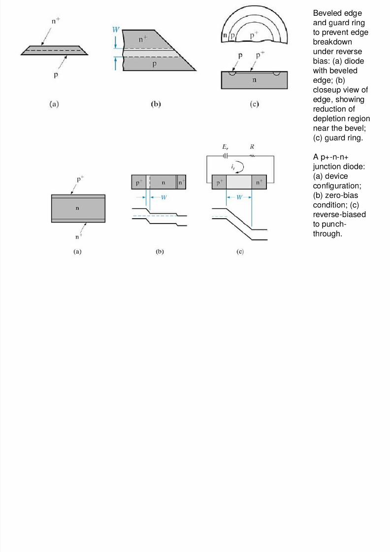
Piecewise-linear approximations of junction diode characteristics: (a) theideal diode; (b) ideal diode with an offset voltage; (c) ideal diode with an offsetvoltage and a resistance to account for slope in the forward characteristic.Want high breakdown and low series resistance for rectifiers. In p+-p-n+ orp+-n-n+ diode, as p or ndoping decreases avalanche breakdown voltage
increases, but punchthrough voltage decreases, andresistance increases. Iflength of region decreases, punchthrough worse, but resistance decreases.
Bevelededge
8/19/2019 microelectronics presentation on semiconductor devices and circuit theory
http://slidepdf.com/reader/full/microelectronics-presentation-on-semiconductor-devices-and-circuit-theory 38/59
Beveled edgeand guard ringto prevent edgebreakdownunder reversebias: (a) diodewith bevelededge; (b)closeup view ofedge, showingreduction ofdepletion region
near the bevel;(c) guard ring.
A p+-n-n+ junction diode:(a) deviceconfiguration;
(b) zero-biascondition; (c)reverse-biasedto punch-through.

8/19/2019 microelectronics presentation on semiconductor devices and circuit theory
http://slidepdf.com/reader/full/microelectronics-presentation-on-semiconductor-devices-and-circuit-theory 39/59
Current in a reverse-biased

8/19/2019 microelectronics presentation on semiconductor devices and circuit theory
http://slidepdf.com/reader/full/microelectronics-presentation-on-semiconductor-devices-and-circuit-theory 40/59
p-n junction due to thermalgeneration of carriers by
(a) band-to-band EHPgeneration, and
(b) generation from a
recombination level.Generation lifetime decreases for
higher trap concentrationsand deeper traps.
τ 2i
GR qn AW I =
2,' == ne I I nkT
qV
o
Similarly, in forward bias, injected
carriers can recombine via trapsin the depletion region unlike in an“ideal” diode.
Highbiaseffects:highlevelinjectionandohmicdrops

8/19/2019 microelectronics presentation on semiconductor devices and circuit theory
http://slidepdf.com/reader/full/microelectronics-presentation-on-semiconductor-devices-and-circuit-theory 41/59
Examples of contactpotential for a heavily
doped p-n junction: (a)at equilibrium; (b)approaching themaximum forward biasV =V0
High bias effects: high level injection and ohmic drops

8/19/2019 microelectronics presentation on semiconductor devices and circuit theory
http://slidepdf.com/reader/full/microelectronics-presentation-on-semiconductor-devices-and-circuit-theory 42/59
Forward and reverse current-voltage characteristics plotted on semi-log scales, withcurrent normalized with respect to saturation current,I0; (a) the ideal forward
characteristic is an exponential with an ideality factor,n = 1 (dashed straight line on log-linear plot). The actual forward characteristics of a typical diode (colored line) have fourregimes of operation; (b) ideal reverse characteristic (dashed line) is a voltage-
independent current =I0. Actual leakage characteristics (colored line) are higher due toeneration in the deletion reion and also show breakdown at hih voltaes.

8/19/2019 microelectronics presentation on semiconductor devices and circuit theory
http://slidepdf.com/reader/full/microelectronics-presentation-on-semiconductor-devices-and-circuit-theory 43/59
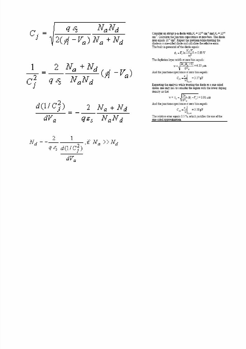
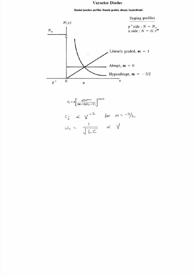
Depletion capacitance of a junction

8/19/2019 microelectronics presentation on semiconductor devices and circuit theory
http://slidepdf.com/reader/full/microelectronics-presentation-on-semiconductor-devices-and-circuit-theory 44/59
(a) p+-n junction showing variation of depletion edge on n side with reverse bias.Electrically, the structure looks like a parallel plate capacitor whose dielectric is the
depletion region, and the plates are the space charge neutral regions; (b) variation ofdepletion capacitance with reverse bias. Neglect x p0 in the p+ material.
p apa a a j
V
QV C ∂
∂ =)(
V QC =
Capacitance represents charge storage:
Semiconductor voltage-dependent small
signal capacitance:
)/)(2 0 d qN V V
A
W
AC
−
==
ε
ε ε
8/19/2019 microelectronics presentation on semiconductor devices and circuit theory
http://slidepdf.com/reader/full/microelectronics-presentation-on-semiconductor-devices-and-circuit-theory 45/59

8/19/2019 microelectronics presentation on semiconductor devices and circuit theory
http://slidepdf.com/reader/full/microelectronics-presentation-on-semiconductor-devices-and-circuit-theory 46/59
8/19/2019 microelectronics presentation on semiconductor devices and circuit theory
http://slidepdf.com/reader/full/microelectronics-presentation-on-semiconductor-devices-and-circuit-theory 47/59

8/19/2019 microelectronics presentation on semiconductor devices and circuit theory
http://slidepdf.com/reader/full/microelectronics-presentation-on-semiconductor-devices-and-circuit-theory 48/59

8/19/2019 microelectronics presentation on semiconductor devices and circuit theory
http://slidepdf.com/reader/full/microelectronics-presentation-on-semiconductor-devices-and-circuit-theory 49/59

8/19/2019 microelectronics presentation on semiconductor devices and circuit theory
http://slidepdf.com/reader/full/microelectronics-presentation-on-semiconductor-devices-and-circuit-theory 50/59
Storage delay time in a p+-n diode

8/19/2019 microelectronics presentation on semiconductor devices and circuit theory
http://slidepdf.com/reader/full/microelectronics-presentation-on-semiconductor-devices-and-circuit-theory 51/59
(a) circuit and input square wave; (b)hole distribution in the n-region as afunction of time during the transient;
(c) variation of current and voltagewith time; (d) sketch of transientcurrent and voltage on the deviceI–V characteristic.
g y p
A long P+-N junction forward bias current is switched for IF1 to IF2 at t = 0. Calculate the stored charge Qpas
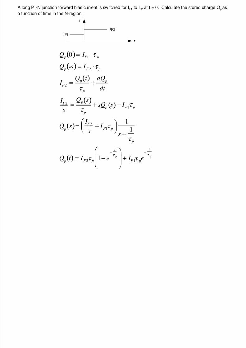
8/19/2019 microelectronics presentation on semiconductor devices and circuit theory
http://slidepdf.com/reader/full/microelectronics-presentation-on-semiconductor-devices-and-circuit-theory 52/59
I
IF1
IF2
τ
Q p 0( )= I F 1 ⋅τ p
Q p∞( ) = I
F 2⋅τ
p
I F 2 =Q
p
t ( )τ
p+
dQ p
dt
I F 2
s=
Q p
s( )τ
p
+ sQ p
s( ) − I F 1
τ p
Q p
s( )= I F 2
s+ I
F 1τ
p 1
s +1
τ p
Q p
t ( )=
I F 2τ
p
1
−e
−t
τ p
+ I
F 1τ
p
e−
t
τ p
p
a function of time in the N-region.
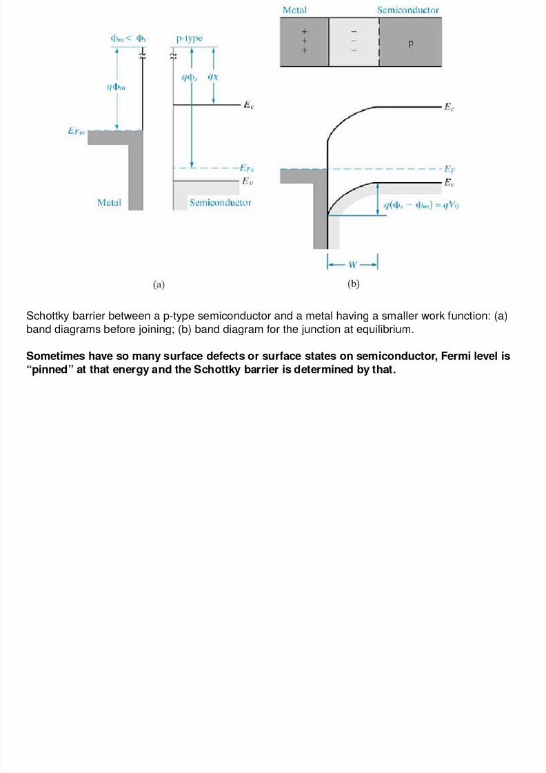
Schottky barrier formed by contacting an n-type semiconductor with a metalh i l kf i

8/19/2019 microelectronics presentation on semiconductor devices and circuit theory
http://slidepdf.com/reader/full/microelectronics-presentation-on-semiconductor-devices-and-circuit-theory 53/59
(a) Band diagrams for the metal and the semiconductor before joining; (b) equilibrium banddiagram for the junction.Work function is the difference between Fermi level and thereference vacuum level.Electronaffinity is the difference between the conduction band and the vacuum level. Electron affinity plus
bandgap gives valence band energy.
having a larger work function
8/19/2019 microelectronics presentation on semiconductor devices and circuit theory
http://slidepdf.com/reader/full/microelectronics-presentation-on-semiconductor-devices-and-circuit-theory 54/59
Effects of forward and reverse bias on the 'unction : (a) forward bias (b) reverse bias (c) typical characteristic.
8/19/2019 microelectronics presentation on semiconductor devices and circuit theory
http://slidepdf.com/reader/full/microelectronics-presentation-on-semiconductor-devices-and-circuit-theory 55/59
Schottky barrier between a p-type semiconductor and a metal having a smaller work function: (a)band diagrams before joining; (b) band diagram for the junction at equilibrium.
Sometimes have so many surface defects or surface states on semiconductor, Fermi level is“pinned” at that energy and the Schottky barrier is determined by that.

8/19/2019 microelectronics presentation on semiconductor devices and circuit theory
http://slidepdf.com/reader/full/microelectronics-presentation-on-semiconductor-devices-and-circuit-theory 56/59
Ohmic metal–semiconductor contacts

8/19/2019 microelectronics presentation on semiconductor devices and circuit theory
http://slidepdf.com/reader/full/microelectronics-presentation-on-semiconductor-devices-and-circuit-theory 57/59
(a) for an n*type
semiconductor
(b) the equilibrium band
diagram for the 'unction
(c) for a p*typesemiconductor
(d) the 'unction at equilibrium.
We get an ohmic contact ifthere is an increase of the
majority carrierconcentration in thesemiconductor due totransfer of carriers fromthe metal after contact.
We can get a “functional”ohmic contact with heavydoping which causes atunnel junction, or bycreating defects which
causes a leaky junction.

8/19/2019 microelectronics presentation on semiconductor devices and circuit theory
http://slidepdf.com/reader/full/microelectronics-presentation-on-semiconductor-devices-and-circuit-theory 58/59
Figure 5—45
An ideal hetero'unction between a p*type$ wide band gap semiconductor an n*type
narrower band gap semiconductor: (a) band diagrams before 'oining (b) band
discontinuities and band bending at equilibrium.
Chapter 5 SUMMARY• 1. Diodes and other semiconductor devices are made by combinations of steps such as oxidation, selective doping (via implant or diffusion),
and deposition of various insulators or metals in concert with etching using patterns formed by photolithography

8/19/2019 microelectronics presentation on semiconductor devices and circuit theory
http://slidepdf.com/reader/full/microelectronics-presentation-on-semiconductor-devices-and-circuit-theory 59/59
and deposition of various insulators or metals in concert with etching, using patterns formed by photolithography.• 2. When we bring a p and n type semiconductor into contact to make a p-n junction diode, carriers diffuse across the junction until we get a
flat Fermi level in equilibrium. A built-in junction potential barrier is formed between the p and n sides which reflects the voltage dropacross the depletion region. This is a dynamic equilibrium, where there is continual diffusion of electrons from the n to the p side (and holesform p to n), but at a reduced rate over the potential barrier, and these fluxes are cancelled by opposing flows of minority carriers diffusing tothe depletion edges and getting swept across the junction.
• 3. The electrostatics of the depletion region is determined by solving the Poisson equation. For uniformly doped abrupt step junctions we getlinearly varying electric fields which are highest at the metallurgical junction. We get a wider depletion region on the more lightly doped
side and equal and opposite depletion charges on the two sides of the junction.• 4. For an ideal Shockley diode, one assumes there is negligible generation-recombination inside the depletion region. In forward bias, the
built-in potential barrier is lowered, making it exponentially easier for majority carriers to diffuse across.• 5. The opposing minority carrier fluxes are unaffected because they are limited by how often the few minority carriers diffuse to the
depletion edges. Far from the junction, the current is carried by drift of the majority carriers, which are injected across the junction to theother side as minority carriers where they give rise to diffusion currents.
• 6. In reverse bias, for ideal diodes, the voltage-independent reverse current is due to the collection of thermally generated minority carrierson either side diffusing to the depletion region, and then being swept across. The current flow from n to p is small, and is the basis of dioderectifiers.
• 7. For high reverse biases, diodes undergo (reversible) breakdown due to quantum mechanical tunneling (Zener mechanism) across a narrowdepletion region for very heavily doped junctions, or due to impact ionization or avalanche multiplication of carriers in a wider depletionregion for lightly doped junctions. For narrow diodes, there can also be punchthrough from one contact to the other.
• 8. Varying the bias leads to diode switching; the diode transient behavior can be found by solving the continuity equation, for example usingLaplace transforms, with suitable initial and boundary conditions.
• 9. Small signal capacitance in a semiconductor device is caused by change of the charge storage as function of bias. There are twocomponents of diode capacitance: depletion capacitance due to exposed dopant charges in the depletion region (dominates in reverse bias),and diffusion capacitance due to stored excess mobile carriers (dominates in forward bias)
• 10. Real diodes can deviate from Shockley “ideal” diodes which have negligible generation-recombination in the depletion region.Generation-recombination in the depletion region increases the diode ideality factor, n, from 1 to 2 in forward bias, and introduces a roughlysquare root voltage dependence of reverse leakage current.
• 11. High level carrier injection for large forward bias, where the injected minority carrier concentration is comparable to the backgroundmajority carrier concentration, also makes n=2. Series resistance effects also play a role for higher currents.
• 12. Graded junctions, where the doping concentrations on either side are not constant, are qualitatively similar to abrupt junctions but areharder to analyze. They have different C-V than abrupt junctions.
• 13. Metal-semiconductor junctions behave as Schottky diodes (if the Fermi level alignments are such that there is a depletion of majoritycarriers in the semiconductor) or ohmic contacts (if there is no depletion region formed in the semiconductor.)
• 14. Junctions between dissimilar semiconductors are called heterojunctions. With respect to a vacuum reference level, one looks at theconduction band edges (electron affinities) and bandgaps to determine the band offsets, and the Fermi levels (work functions) to determinethe direction of carrier transfer. Electrons flow from the high to low Fermi level regions, and holes the opposite way.