
Microelectronics Department - Lirmm
78
Microelectronics Department 2011 ACTIVITY REPORT 161 rue Ada - 34095 Montpellier - Cedex 05 - FRANCE Tel: 33 (0)4 67 41 85 85 - Fax: 33 (0)4 67 41 85 00 - www.lirmm.fr
Transcript of Microelectronics Department - Lirmm

Microelectronics Department
2011 ACTIVITY REPORT
161 rue Ada - 34095 Montpellier - Cedex 05 - FRANCE Tel: 33 (0)4 67 41 85 85 - Fax: 33 (0)4 67 41 85 00 - www.lirmm.fr

Microelectronics Department – 2011 Activity Report

Microelectronics Department – 2011 Activity Report
Table of Contents
Page 3 A Few Words about LIRMM and the Microelectronics Department LIRMM The Microelectronics Department
Page 5 Staff members Key numbers List of members
Page 7 Organization SysMIC project DEMAR project
Page 9 Summary of 2011 Activities PART ONE - Analysis and Models for Circuit Design PART TWO - Test of Integrated Circuits and Systems
o Digital Testing o Power-Aware Testing o Memory Testing o Test & Security o Analog & RF Testing
PART THREE - Design and Test of MEMS PART FOUR - Adaptive Circuits and Systems PART FIVE - Biomedical Circuits and Systems
Page 65 Summary of 2011 Publications
Page 66 List of PhD Thesis defended in 2011
Page 67 Microelectronics Department Profile
Role and Involvement at the International and National Levels International Academic Cooperation National and European Research Projects Industrial Relationships ISyTest – A Joint Lab between LIRMM and NXP Technological Platforms
Page 74 Sample Gallery

Microelectronics Department – 2011 Activity Report 3
A Few Words about LIRMM
Montpellier Laboratory for Informatics, Robotics and Microelectronics (LIRMM) is a research laboratory supervised by both Montpellier University (Université Montpellier 2) and the French National Center for Scientific Research (CNRS). With a staff of 405 people (including permanent and temporary employees, as well as Ph.D. and Post-Doc students), LIRMM is one of the most important academic laboratories in France. Its research activities position the LIRMM at the heart of Information and Communication Technologies (ICT) and sciences. The spectrum of research activities covered by LIRMM is very broad, and includes:
Algorithms, databases, information systems, software engineering, artificial intelligence, networks, arithmetic, optimization, natural language and bioinformatics,
Design of mechanical systems, modeling, identification, control and perception, Design and verification of integrated, mobile and communicating systems
The combination of these skills results in interdisciplinary academic or industrial research projects conducted at national and international levels.
One of the LIRMM strengths is that each field of scientific expertise covers theory, tools, experiments and applications. The research works generally find applications in a great diversity of domains, such as biology, chemistry, telecommunications, health, environment, agronomy, etc., as well as in domains directly related to the own lab activities: informatics, electronics, and automation.
LIRMM is a laboratory dedicated to "produce” knowledge (more than 300 international publications per year) and educate future researchers (Masters, PhDs, post-docs), and is involved in a strong economical “dynamic”: industrial partnerships, innovative start-ups, national and international scientific leadership, etc.
The laboratory is organized in three departments: Informatics, Robotics and Microelectronics.

Microelectronics Department – 2011 Activity Report 4
A Few Words about the Microelectronics Department
The Microelectronics department is specialized in the research of innovative solutions to model, design and test complex integrated circuits and systems. Such systems are characterized by a high complexity, elevated performances, a high heterogeneity, and a 2D or 3D integration into a single package.
The expertise of the Department covers the following strategic topics:
Development of new generations of processor architectures for applications like 4G mobile phones, signal and image processing, or multimedia;
Design for testability, and test of integrated circuits and systems, which include all activities on modeling, detection and diagnostic of physical failures;
Design, integration and test of micro-systems based on sensors and actuators; Secured design for the confidentiality and integrity of communications (in banking transactions for
example); Design of circuits for the health and medical domains, with applications like neuro-stimulation
systems implanted the human body.
The research activities are multidisciplinary and require skills in computer science, mathematics, physics, life sciences, etc. This allows the research team to provide answers to the various and numerous scientific, societal and economical challenges of today and tomorrow Microelectronics.
To conduct these research activities, the Department relies on a hundred of persons, including full-time researchers, professors, PhD students, post-doc students, research engineers and technicians. Owing to its high-level scientific production, its academic collaborations, its implication in numerous national and international research programs, its participation to the creation of start-up companies, and its activities of transfer and valorization towards the industry sector, the Department is now recognized as an essential actor in the landscape of the French and international scientific research in Microelectronics.

Microelectronics Department – 2011 Activity Report 5
Staff: 98 People
During the year 2011, the Microelectronics Department was composed of 29 permanent researchers (from University Montpellier 2, CNRS and INRIA), 1 associate member, 11 Post-Doctoral students, 47 PhD students, 1 ATER, 9 research engineers, technicians and administrative staff and a dozen of Master students.
Head of Department Patrick Girard, CNRS Research Director
Deputy-Heads of Department Serge Bernard, CNRS Researcher Laurent Latorre, Associate Professor at Montpellier University
Full researchers and professors (29) Florence Azais, CNRS Researcher Nadine Azemard-Crestani, CNRS Researcher Pascal Benoit, Associate Professor at University of Montpellier Serge Bernard, CNRS Researcher Yves Bertrand, Professor at University of Montpellier Alberto Bosio, Associate Professor at University of Montpellier Guy Cathebras, Professor at University of Montpellier Mariane Comte, Associate Professor at University of Montpellier Denis Deschacht, CNRS Research Director Giorgio Di Natale, CNRS Researcher Luigi Dilillo, CNRS Researcher Sophie Dupuis, Associate Professor at University of Montpellier Marie-Lise Flottes, CNRS Researcher Jérôme Galy, Associate Professor at University of Montpellier Patrick Girard, CNRS Research Director David Guiraud, INRIA Research Director Laurent Latorre, Associate Professor at University of Montpellier Frédérick Mailly, Associate Professor at University of Montpellier Philippe Maurine, Associate Professor at University of Montpellier Pascal Nouet, Professor at University of Montpellier Serge Pravossoudovitch, Professor at University of Montpellier Michel Renovell, CNRS Research Director Michel Robert, Professor at University of Montpellier Bruno Rouzeyre, Professor at University of Montpellier Gilles Sassatelli, CNRS Researcher Director Fabien Soulier, Associate Professor at University of Montpellier Aida Todri, CNRS Researcher Lionel Torres, Professor at University of Montpellier Arnaud Virazel, Associate Professor at University of Montpellier
Associate members (1) Jean-Marc Gallière, PRAG Professor at University of Montpellier

Microelectronics Department – 2011 Activity Report 6
Ph.D. students (47)
Postdoctoral research fellows (11)
Syed Zahid Ahmed Renan Alves Fonseca Marina Aparicio Joao Azevedo Yeter Akgul Lyonel Barthe Kaouthar Bousselam Florent Bruguier Raphael Brum Rémi Busseuil Mathieu Carbone Luis Vitorio Cargnini Jean Da Rolt Amine Dehbaoui Pierre-François Desrumaux Florian Devic Jérome Dibattista Mouhamadou Dieng Haythem El Ayari Hyassine Fkih Yoann Guillemenet Souha Hacine Nicolas Hebert Fanny le Floch
Feng Lu Imen Mansouri Gabriel Marchesan Almeida Baptiste Marechal Pierre-Didier Mauroux Carolina Metzler Huy Binh Nguyen Guilherme Perin François Poucheret Nicolas Pous Ahmed Rekik Olivier Rossel Zhenzhou Sun Sébastien Tiran Karim Tobich Georgios Tsiligiannis Duc Anh Tran Miroslav Valka Bruno Vaquie Sameer Varyani Lionel Vincent Fangmei Wu Leonardo Zordan
Guilherme Bontorin Jonathan Coulombe Jérémie Crenne Norbert Dumas Raphael Garibotti Vincent Kerzerho Luciano Ost Rodrigo Possamai Bastos Paolo Rech Carlo Trigona Zequi Wu
Temporary professors and researchers (1) Olivier Leman, Temporary associate professor and researcher (ATER)
Research engineers, technicians and administrative staff (9) Morgan Bourree, research engineer Samuel Cohet, research engineer Laurent De Knyff, technician at Montpellier University Caroline Drap, secretary Thierry Gil, CNRS research engineer Ludovic Guillaume-Sage, technician Régis Lorival, CNRS research engineer Olivier Potin, research engineer Jérémie Salles, research engineer
Guest professors (4) Paolo Bernardi, Politecnico di Torino, Italy Sandip Kundu, Massachussets University , USA Fernando Moraes, PUCRS, Brazil Brahim Mezghani, University of Sfax, Tunisia

Microelectronics Department – 2011 Activity Report 7
Organization
Research activities carried out by the Microelectronics Department are organized within two major research project teams:
SysMIC: Design and Test of Microelectronic Systems DEMAR: Deambulation and Artificial Movement (joint team between LIRMM and INRIA, and joint
team between Robotics and Microelectronics departments)
SysMIC
The overall objective of the SysMIC team is to propose innovative solutions to model, design and test today’s and tomorrow’s integrated circuits and systems. The overall challenges that are addressed are: complexity, performances, power consumption, heterogeneity (digital, analog, RF, memory, MEMS, FPGA, etc.), reliability and robustness (ageing, impact of environment), manufacturing related issues (variability, high defect density), communications (network-on-chip, wireless, sensor networks), and emerging technologies (physical phenomena to understand, to model and to integrate).
The four main research areas are:
Analysis and Models for Circuit Design to develop analysis methods and models for electrical phenomena (e.g. crosstalk) and performance estimation (delay, power consumption), and to develop flows for process variability monitoring and security evaluation. The topics include:
Performance analysis Process variability monitoring flows Security evaluation (through a platform) Counter-measures for secured circuits Attack definition (anticipating threats)

Microelectronics Department – 2011 Activity Report 8
Test of Integrated Circuits and Systems to develop Design-for-Test techniques for complex systems (to ease test application and increase test efficiency), to develop fault models, methods, algorithms and tools to test manufacturing defects and deal with reliability issues, and for detection, diagnosis and in situ repair of various types of malfunctions. The topics include:
Fault modeling Test of analog, mixed-Signal & RF circuits Test of memories (SRAM, Flash, MRAM) Test of low power designs Test of secured circuits Wireless testing Fault tolerance and test of fault tolerant structures Test of System-on-Chip (SoC), System-in-Package (SiP), and 3D ICs Fault diagnosis
Design and Test of MEMS to develop innovative solutions to promote the integration of low-cost MEMS devices and dedicated electronic interfaces relying on standard technologies. The topics include:
MEMS integration CAD of heterogeneous systems Electronic Interfaces Design & Test of MEMS
Adaptive Circuits and Systems to explore and design self-aware / adaptive circuits & systems: online decision making for optimizing performance, power, reliability, security. The topics include:
Adaptive MPSoCs Fault-tolerant MPSoCs Virtualization techniques Hybrid circuits (MRAM/CMOS) Emerging Technologies Secure systems and architectures Self-organizing sensor networks
DEMAR
The overall objective of the DEMAR team is to propose complete Functional Electrical Stimulation (FES) systems based on the patients’ demand discussed with the medical staff. The overall challenges that are addressed are: selectivity for stimulation and recording, power management, complexity and heterogeneity, physiological constraints, and safety for the patient (dependable systems). The main research area is the Development of Micro-Circuits for Neuro-Prothesis. The topics include:
Distributed architecture (stimulation and recording units) Implantable micro-stimulator Modeling and recording of physiological signals Signal processing for ENG recording Design for Dependability

Microelectronics Department – 2011 Activity Report 9
Summary of 2011 activities
I. Analysis & Models for Circuit Design 10
II. Test of Integrated Circuits & Systems - Digital Testing - Reliability - Power Aware Testing - Memory Testing - Test & Security - Analog & RF Testing
15
III. Design & Test of MEMS 41
IV. Adaptive Circuits & Systems 49
V. Biomedical Circuits & Systems 59

Microelectronics Department – 2011 Activity Report 10
Analysis and Models for Circuit Design Department
Microelectronics Department – 2011 Activity Report 11
Interconnect Design for a 32nm Technology
D. DESCHACHT Contact : [email protected]
Partners: LAHC, University of Chambery Topic: Signal Integrity
When high speed integrated circuits technology scales down from one node to the other, ITRS suggests a reduction in size by a factor of around square of 2, and recommends 17% of improvement on performance. With the dimension shrink, the IC’s speed increase gained on active devices is partially loosed. This is mainly due to interconnects delays increase as dimensions of interconnects are shrunk to satisfy integration requirement. Moreover, from the 45 nm generation, worrying crosstalk (XT) levels are expected. These XT levels are particularly noticeable in the intermediate metal level of the Back-End of Line (BEOL) stack which contains relatively
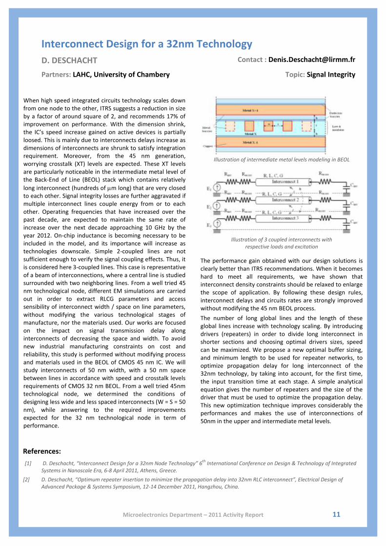
long interconnect (hundreds of m long) that are very closed to each other. Signal integrity losses are further aggravated if multiple interconnect lines couple energy from or to each other. Operating frequencies that have increased over the past decade, are expected to maintain the same rate of increase over the next decade approaching 10 GHz by the year 2012. On-chip inductance is becoming necessary to be included in the model, and its importance will increase as technologies downscale. Simple 2-coupled lines are not sufficient enough to verify the signal coupling effects. Thus, it is considered here 3-coupled lines. This case is representative of a beam of interconnections, where a central line is studied surrounded with two neighboring lines. From a well tried 45 nm technological node, different EM simulations are carried out in order to extract RLCG parameters and access sensibility of interconnect width / space on line parameters, without modifying the various technological stages of manufacture, nor the materials used. Our works are focused on the impact on signal transmission delay along interconnects of decreasing the space and width. To avoid new industrial manufacturing constraints on cost and reliability, this study is performed without modifying process and materials used in the BEOL of CMOS 45 nm IC. We will study interconnects of 50 nm width, with a 50 nm space between lines in accordance with speed and crosstalk levels requirements of CMOS 32 nm BEOL. From a well tried 45nm technological node, we determined the conditions of designing less wide and less spaced interconnects (W = S = 50 nm), while answering to the required improvements expected for the 32 nm technological node in term of performance.
Illustration of intermediate metal levels modeling in BEOL
Illustration of 3 coupled interconnects with
respective loads and excitation
The performance gain obtained with our design solutions is clearly better than ITRS recommendations. When it becomes hard to meet all requirements, we have shown that interconnect density constraints should be relaxed to enlarge the scope of application. By following these design rules, interconnect delays and circuits rates are strongly improved without modifying the 45 nm BEOL process.
The number of long global lines and the length of these global lines increase with technology scaling. By introducing drivers (repeaters) in order to divide long interconnect in shorter sections and choosing optimal drivers sizes, speed can be maximized. We propose a new optimal buffer sizing, and minimum length to be used for repeater networks, to optimize propagation delay for long interconnect of the 32nm technology, by taking into account, for the first time, the input transition time at each stage. A simple analytical equation gives the number of repeaters and the size of the driver that must be used to optimize the propagation delay. This new optimization technique improves considerably the performances and makes the use of interconnections of 50nm in the upper and intermediate metal levels.
References:
[1] D. Deschacht, “Interconnect Design for a 32nm Node Technology” 6th
International Conference on Design & Technology of Integrated Systems in Nanoscale Era, 6-8 April 2011, Athens, Greece.
[2] D. Deschacht, “Optimum repeater insertion to minimize the propagation delay into 32nm RLC interconnect”, Electrical Design of Advanced Package & Systems Symposium, 12-14 December 2011, Hangzhou, China.

Microelectronics Department – 2011 Activity Report 12
SSTA framework for process variability monitoring
N. AZEMARD, P. MAURINE, Z.WU Contact : [email protected]
Partners: Eniac / MODERN, I3M Topic: Models and methods for circuit design
With the « More Moore » and low power trends, optimizing or only well predicting the final performances of digital circuits become more and more difficult. Indeed, variability and hardness to model accurately transistor behavior impede the dimension scaling benefits. Current design methodologies generally use guard margins to prevent from the incertitude generated by these limits and to guarantee functional yield. But as we go in the nanometer era, the use of margin is not efficient anymore, because of an increasing over-design, limiting optimizations and decreasing both parametric and functional yield.
In order to increase the robustness to uncertainty during the design levels and to have better performance analysis, we propose a SSTA Framework Based on Moments Propagation (Figure1). We introduce a new statistical PDF propagation approach built on two concepts in probability theory: conditional mean and conditional variance. Our objective is to develop a simple and practical timing approach considering effect of structure correlations, input slope and output load variations. Such objective causes the introduction of new way to do cells timing characterization: log-normal distribution based model as input signal and inverters as charge. The proposed SSTA flow gives us satisfactory estimate of path delay distribution with maximal relative error 5% and 10% respectively on mean and on standard deviation.
The SSTA engine has been and continues to be verified in collaboration with STMicroelectronics in Crolles in France and the CEA-Leti in Grenoble in France. We have implemented the specific methodology called SSTA (Statistical Static Timing Analysis). We could verify that this SSTA flow allows performing statistical analysis on timing performances and accurately observing process variation effects on delays. This work is made in collaboration with the I3M lab of Montpellier.
We attempt to tackle the problem never been mentioned: estimate of structure correlations, which comes from the fact that output signal of one cell is input signal of the next stage.
More, face to the success of the first edition of the specific workshop on CMOS variability (VARI 2010) that we had organized in 2010 in Montpellier, we have decided to continue this workshop. The second edition has been held in Grenoble on May 30-31, 2011 (Web site : http://www.vari-cmos.org/). It has been organized by the CEA-Leti and the program chair has been the LIRMM. The VARI meeting answers to the need to have an European event on variability, where industry and academia meet to discuss. The VARI objective has to provide a forum to discuss and investigate the CMOS variability problems in methodologies and tools for the design of upcoming generations of integrated circuits and systems. The technical program has focused on timing, performance and power consumption as well as architectural aspects with particular emphasis on modeling, design, characterization, analysis and optimization of variability.
Figure 1: The developed SSTA flow.
References:
[1] Rebaud B., Belleville M., Beigne E., Bernard C., Robert M., Maurine P., Azemard N., "Timing Slack Monitoring under Process and environmental variations : application to a DSP performance optimization", Microelectronics Journal, Vol.42, Issue 5, May 2011, p.718-132
[2] Wu Z., Maurine P., Azemard N., Ducharme G., "Statiscal Timing Characterization of Standard Cells with Semi-Monte-Carlo Method",VARI 2011 : Second European Workshop on CMOS Variaility, Grenoble, France, May 30-31, 2011.
[3] Wu Z., Maurine P., Azemard N., Ducharme G., "Characterizing Statistical Cells Timing Metrics with Semi-Monte-Carlo Method”, VLSI-SoC 2011, IFIP/IEEE VLSI-SoC 2011 - International Conference on Very Large Scale Integration, 3-5 Octobre 2011, Hong-Kong, Chine.
Microelectronics Department – 2011 Activity Report 13
Electromagnetic Side-Channel Analyses and Fault Injection
P. MAURINE, L. TORRES, M. ROBERT Contact : [email protected]
Partners: STMicro, CEA, DGA, ENSMSE, LaHC, I3M, IES, PUCRS Topic: Secure Circuit Evaluation
Physical Attacks aim at disclosing secret information hidden in secure circuits such as smart cards. Among the known attacks, one may identify two extremely efficient and low cost kinds of attacks:
- Side Channel Attacks are based on the statistical treatment of numerous observations of a physical leakage
- While Fault Attacks allow disclosing secret data by comparing faulty responses of secure IC to correct ones.
Within this context, the goal of this project is to evaluate the threat related to both Side Channel Attacks and Fault Attacks based on the exploitation of EM waves.
More precisely, this project aims at adapting or developing specific attacks exploiting the interesting properties of EM waves, both from a practical and a statistical point of views. The project also aims at defining ad-hoc countermeasures (at the right cost) against all newly identified threats. Involved People at LIRMM T. Ordas (Ph.D. 06-09), V. Lomne (Ph. D. 07-10), A. Dehbaoui (Ph. D. 07-10), F. Poucheret (Ph. D. 09-12), S. Tiran (Ph. D. 10-13), K. Tobich (Ph. D. 10-13), B. Vaquie (Ph. D. 10-13), G. Perin (Ph. D. 11-14), M. Carbone (Ph. D. 12-15), L. Torres, M. Robert, P. Maurine Related Projects
- Calisson 1, 2007-2010, Pole de Compétitivité Mondial SCS - Calisson 2, 2011-2014, Pole de Compétitivité Mondial SCS - Prosecure, 2010-2013, OSEO - DGA PEA PREVA 2012-2013 - ANR ARPEGE EMAISeCI
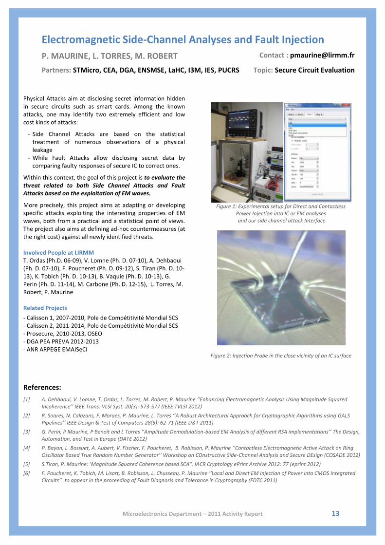
Figure 1: Experimental setup for Direct and Contactless
Power Injection into IC or EM analyses and our side channel attack Interface
Figure 2: Injection Probe in the close vicinity of an IC surface
References:
[1] A. Dehbaoui, V. Lomne, T. Ordas, L. Torres, M. Robert, P. Maurine ‘’Enhancing Electromagnetic Analysis Using Magnitude Squared Incoherence’’ IEEE Trans. VLSI Syst. 20(3): 573-577 (IEEE TVLSI 2012)
[2] R. Soares, N. Calazans, F. Moraes, P. Maurine, L. Torres ‘’A Robust Architectural Approach for Cryptographic Algorithms using GALS Pipelines’’ IEEE Design & Test of Computers 28(5): 62-71 (IEEE D&T 2011)
[3] G. Perin, P Maurine, P Benoit and L Torres ‘’Amplitude Demodulation-based EM Analysis of different RSA implementations’’ The Design, Automation, and Test in Europe (DATE 2012)
[4] P. Bayon, L. Bossuet, A. Aubert, V. Fischer, F. Poucheret, B. Robisson, P. Maurine ‘’Contactless Electromagnetic Active Attack on Ring Oscillator Based True Random Number Generator’’ Workshop on COnstructive Side-Channel Analysis and Secure DEsign (COSADE 2012)
[5] S.Tiran, P. Maurine: ’Magnitude Squared Coherence based SCA“. IACR Cryptology ePrint Archive 2012: 77 (eprint 2012)
[6] F. Poucheret, K. Tobich, M. Lisart, B. Robisson, L. Chusseau, P. Maurine ‘’Local and Direct EM Injection of Power into CMOS Integrated Circuits’’ to appear in the proceeding of Fault Diagnosis and Tolerance in Cryptography (FDTC 2011)

Microelectronics Department – 2011 Activity Report 14
Physical Design and Reliability Issues of Three-Dimensional ICs
A. TODRI, A. BOSIO, L. DILILLO, P. GIRARD, A. VIRAZEL Contact : [email protected]
Partners: Univ. of Massachusetts, USA Topic: Power/Thermal Integrity
Recent advancements in semiconductor processing technologies have enabled three dimensional circuit design and implementation of heterogeneous systems in the same platform, i.e. Flash, DRAM, SRAM placed atop logic devices and microprocessor cores. 3D integration results in shorter interconnect lengths, greater device density and enhanced performance. However, the densely packed vertical tiers introduce significant power and thermal integrity challenges compared to 2D integration.
Due to the increased power density and greater thermal resistance to heat sink, thermal integrity is a crucial challenge for reliable 3D integration. High temperatures can degrade the reliability and performance of interconnects and devices. Power/ground network resistivity is a function of temperature, thus at nodes with high temperature, voltage droop values become even worse. Furthermore, the large amount of current on power and ground networks flowing for significant amount of time can ultimately elevate the temperature and cause Joule heating phenomena and electromigration. Thus, voltage droop and temperature are interdependent and should be considered simultaneously during analysis. Fig.1a shows an illustration of a 3D system where voltage droop tends to increase for tiers further away from package (controlled-collapse chip-connection (C4) bumps) and close to heat sink while temperature increases for tiers further away from heat sink and near to package pins.
The objective of this work is to investigate power and thermal integrity issues in 3D ICs by performing a comprehensive electro-thermal analysis. Additionally, fast and accurate RLC models are developed for studying TSVs, power/ground networks, package pins and switching circuits. Our electro-thermal analysis provides detailed voltage droop and thermal map for each tier as shown in Fig 1.b. Based on the analysis results, optimization of power/ground and clock networks can be performed while ensuring power and thermal integrity.
Heat Sink
Isolation layer
Tier 4
Tier 1
Tier 2
Tier 3
Top metal layers
Bottom metal layers
(a)
(b)
Figure 1. (a) Illustration of a four tier 3D IC, and (b) tier based voltage/temperature distributions, voltage droop and thermal maps generated from electro-thermal analysis tool.
References:
[1] A. Todri, A. Bosio, L. Dilillo, P. Girard, S. Pravossoudovitch, A. Virazel, “Simultaneous Power and Thermal Integrity Analysis for 3D Integrated Systems,” IEEE International Workshop on the Impact of Low Power on Test and Reliability (LPonTR’11), 2011.
[2] A. Todri, S. Kundu, P. Girard, A. Bosio, L. Dilillo, A. Virazel, “A Study of Tapered 3D TSVs for Power and Thermal Integrity,” accepted and to appear in IEEE Transactions on Very Large Scale Integration (VLSI) Systems, 2012.

Microelectronics Department – 2011 Activity Report 15
Test of Integrated Circuits & Systems Department

Microelectronics Department – 2011 Activity Report 16
Power Supply Noise and Ground Bounce Aware Pattern Generation for Delay Testing
A. TODRI, A. BOSIO, L. DILILLO, P. GIRARD, S. PRAVOSSOUDOVITCH, A. VIRAZEL
Contact : [email protected]
Topic: Delay Testing, Speed Binning
As technology scales down, the effects of power supply noise and ground bounce are becoming significantly important. In the existing literature, it has been shown that excessive power supply noise can affect the path delay, while ground bounce is either neglected or assumed similar to power supply noise. Our work performs a detailed study of combined and uncorrelated power supply noise and ground bounce and their impact on the path delay. Our analyses show that different combination of power supply noise and ground bounce can lead to either delay speed-up or slow-down.
Our objective is to generate test patterns such that the combined effects of power supply noise and ground bounce are considered on circuit delay analysis. The impact of noise on delay is highly depended on the applied input patterns. Our research seeks to provide mathematical models to represent the circuit based on the physical extracted data after the circuit is placed & routed with power/ground grids. We propose close-form mathematical models to capture the impact of input patterns on path delay in the presence of power supply noise and ground bounce. We use a simulated annealing (SA) based approach to find patterns that maximize the critical path delay. In contrast to previous works which initially aim to find patterns for maximum supply noise and then compute delay, our method targets directly to find the worst case delay which might not necessarily occur under worst case power supply noise due to the speed-up/slow-down phenomena. Our method generates patterns that sensitize the path and also cause such power supply noise and ground bounce that leads to the maximum path delay.
Figure 1 shows a sample two buffer circuit and its power and ground networks. As the gates are placed in different
locations on the chip, the amount of power supply noise and ground bounce that they experience can vary significantly among them. Such variations on the power and ground networks lead to variations on the path delay which can be either a speed-up or slow-down effect.
Gate 1
Gate 2
VDD
VDD
VDD VDD
GND GND
GND
GND
Path under investigation
(a)
Lpkg
LgridRgrid
Grid segments
RpkgPackage
Ground network
Gate 1
Gate 2Rpwr1 Lpwr1
Rgnd1 Lgnd1
Rgnd2 Lgnd2
C4 bumps
Power network
Rpwr2 Lpwr2
(b)
Figure 1. (a) An illustration of gate placement on chip and (b) representative model for two-stage buffer circuit used for path delay analysis in the presence of power supply noise and ground bounce.
References:
[1] A. Todri, A. Bosio, L. Dilillo, P. Girard, S. Pravossoudovitch, A. Virazel, “A Study of Path Delay Variations in the Presence of Uncorrelated Power and Ground Noise,” IEEE Symposium on Design and Diagnostics of Electronic Circuits and Systems, pp. 189-194, 2011.
[2] A. Todri, A. Bosio, L. Dilillo, P. Girard, S. Pravossoudovitch, A. Virazel, “Power Supply Noise and Ground Bounce Aware Pattern Generation for Delay Testing,” IEEE International NEWCAS Conference, pp.73-76, 2011.
[3] A. Todri, A. Bosio, L. Dilillo, P. Girard, A. Virazel, “Uncorrelated Power Supply Noise and Ground Bounce Consideration for Test Pattern Generation,” submitted to IEEE Transactions on VLSI Systems (VLSI), 2011.

Microelectronics Department – 2011 Activity Report 17
Defect Modeling in Nanometric CMOS Technologies
M. APARICIO, F. AZAIS, Y. BERTRAND, M. COMTE, M. RENOVELL
Contact : [email protected]
Partners: Universities of Passau & Freiburg, CCUFB (Centre de Coopération Universitaire Franco-Bavaroise)
Topic: Defect modeling, defect-oriented testing
The general principle of digital Integrated Circuit (IC) testing consists in highlighting an awkward behavior that may result from a physical failure or a signal integrity matter. The general objective of the studies carried out in this topic is to study the electrical behavior of ICs affected by physical failures on the one hand and by undesired power variations on the other hand in order to propose realistic fault models for CMOS nanometric technologies meant to facilitate efficient IC tests.
The traditional stuck-at fault model does not manage any longer to cover all possible circuit failures. Some new models have appeared to complement the traditional ones. Let us mention the parametrical resistive short model that takes into account the resistance of the defects, and the compact model for transistors affected by a Gate-Oxide Short (GOS), both models developed by the LIRMM team, which has become expert in this field. These new fault models now consider the notion of defect random parameters (for instance its size, its resistance value), which are unpredictable by nature. Regarding signal integrity matters, a fine analysis of the noise in the power supplies has led to a better understanding of the affected circuit. Furthermore, with nanometric technologies emergence, new types of defects, which impact on the system behavior used to be negligible, tend to become as significant as previously known defects with comparable effects. One could mention ground bounce, IR drop or NBTI (Negative Bias Temperature Instability). It seems therefore necessary to consider these “new” defect impact as an additional contribution to the sum of defects and to take them into account within the framework of behavioral modeling.
A dynamic analysis of the electrical effects caused by a resistive short between two gate outputs has recently been carried out. This analysis takes into account the crosstalk capacitance between the involved lines.
The electrical behavior of the node affected by the resistive short therefore depends not only on the parametrical value of the defect but also on the crosstalk capacitance as well as on the skew between input signal transitions on both lines. Figure 1 shows the transition delay evolution of one affected gate’s output versus the skew for different defect resistance values. A mathematical model has been proposed, validated and integrated into a fault simulator by the University Albert-Ludwigs of Freiburg.
Figure 1: Electrical simulation of the delay induced by a crosstalk aggravated resistive short defect
Current work concerns the analysis and modeling of the impact of voltage power drop (or IR-Drop) on the propagation delay of gates in nanometric CMOS technologies. The IR-Drop effect is generated by the parasitic resistors of the power grid. The voltage power drop may occur at a power supply via when several physically neighboring transistors fed by the power via experience simultaneous logic transitions in response to a change in the circuit inputs. Therefore, the IR-Drop propagation is closely related to the power grid structure. The voltage power drop may cause timing faults that must be taken into account in the fault tests. Our objective is to analyze and model how the voltage power drop propagates and dissipates in time and space and how it affects the neighboring gates connected to the same power supply.
References:
[1] Houarche N., Comte M., Renovell M., Czutro A., Engelke P., Polian I., Becker B., “An Electrical Model for the Fault Simulation of Small Delay Faults Caused by Crosstalk Aggravated Resistive Short Defects”, VTS'09: 27th VLSI Test Symposium, USA, pp. 21-26, 2009
[2] Houarche N., Czutro A., Comte M., Engelke P., Polian I., Becker B., Renovell M., “Deriving an Electrical Model for Delay Faults Caused by Crosstalk Aggravated Resistive Short Defects”, LATW'09: 10th Latin-American Test Workshop, Brazil, 2009

Microelectronics Department – 2011 Activity Report 18
Modeling Gate Delay Faults by means of Transition Faults
A. BOSIO, P. GIRARD, S. PRAVOSSOUDOVITCH Contact : [email protected]
Partners: PICS CNRS / Politecnico di Torino Topic: Test & Diagnosis
Nowadays, electronics products present various issues that become increasingly important with CMOS technology scaling. In particular, high operation speed (and thus high frequency) is a mandatory request. These needs influence not only the design of devices, but also the choice of appropriate test schemes that have to deal between production yield, test quality and test cost. Due to the advances in manufacturing technologies and more aggressive clocking strategies used in modern design, more and more defects lead to failures that can no longer be modeled by classical stuck-at faults. Numerous actual failures exhibit timing or parametric behaviors that are not represented by stuck-at faults. Such failures have to be taken into account during the test process in order to reach acceptable DPM (Defect per Million) figures.
Testing for performance, required to catch timing or delay faults, is therefore mandatory and is often done through at-speed scan testing for logic circuits. At-speed scan testing consists of using a rated system (nominal) clock period between launch and capture for each delay test pattern, while a longer clock period is normally used for scan shifting (load and unload cycles).
The most widely used fault models targeting timing related failures are the Transition Fault Model (Figure 1.a) and the Gate Delay Fault Model (Figure 1.b). The Transition Fault Model is a qualitative delay fault model. It assumes that the delay at the fault site is large enough to cause logic failure. The main advantage of the Transition Fault Model is that it does not require to explicitly considering delay size during fault simulation. Conversely, the Gate Delay Fault Model is a quantitative delay fault model since a delay size has to be defined (or assumed) in advance. This fault model is more accurate with respect to the Transition Fault Model, but the need to take into account the delay size makes harder fault simulation and test generation.
In this work we present a methodology aimed at representing a Gate Delay Fault as a set of Transition Delay Faults in the propagation paths of the affected port. The proposed equivalence introduces a significant advantage with respect to other methods considering the Gate Delay Fault effects through timing simulation; in fact, by considering Transition Delay Faults only, we shift the analysis to a quantitative level of abstraction instead of explicitly considering the delay size and the delay effect over the circuit.
Figure 1. Example of delay fault models: a) Transition Delay Fault, b) Gate Delay Fault.
The set of Transition Faults identified as equivalent to a Gate Delay Fault also depends on the sensitization path and changes even for the same delay according to the incoming path from a primary input to the considered gate. Therefore, the proposed technique consists in the analysis of the circuit, traversing both the sensitization and the propagation paths.
As a difference with previous works, we introduce a preliminary step w.r.t. conventional fault simulation. By using the proposed methodology, we “prepare” the fault list before performing the fault simulation process, accounting only for Transition Delay Faults (i.e., without adding timing information). Moreover, a classification of the delay size ranges is obtained as a by-product of the performed analysis; different delay sizes may possibly lead to “no effect”, to “limited effect” or to “gross effect”.
References:
[1] A. Bosio, Paolo Bernardi, Patrick Girard, Serge Pravossoudovich, Matteo Sonza Reorda, “On the Modeling of Gate Delay Faults by means of Transition Delay Faults”, IEEE International Symposium on Defect and Fault Tolerance in VLSI and Nanotechnology Systems, pp. 226 – 232, 2011.

Microelectronics Department – 2011 Activity Report 19
Timing Issues of Transient Faults in Concurrent Error Detection Schemes
R. P. BASTOS, G. DI NATALE, M. L. FLOTTES, B. ROUZEYRE Contact : [email protected]
Partners: Catrene TOETS Topic: Fault Tolerance
IC-based systems are liable to encounter transient voltage variations induced by uncontrollable environmental conditions or even intentional perturbations. These effects – so-called transient faults (TFs) – may produce soft errors (SEs), i.e. storage of erroneous values while the circuit is in operation. These TFs must be quickly detected before circuit’s failure in systems requiring high availability. Moreover, TFs can be used as a form of fault-based attack to infer secret data during the execution of encryption operations in security applications.
Related researches until the end of 20th century were focused on protecting systems against TFs arising in memory elements, which were considered to be the system’s most vulnerable circuits. Hence, many concurrent error detection and/or correction mechanisms were thus proposed to mitigate direct SEs induced by TFs originating in memory circuits. Nevertheless, in the last decade deeper-submicron technologies as well as novel classes of malicious fault-based attacks – e.g. differential fault analysis (DFA) – have also pushed on the use of countermeasures against indirect SEs due to TFs arising in system’s combinational logic circuits.
The traditional solution to face this issue is adding information, spatial, or time redundancy to the circuit. When a circuit’s component temporarily fails, a redundant copy detects, eventually corrects, the produces error. In theory, such redundancy-based schemes cope very efficiently with single SEs caused by short-duration Single TFs (STF, short meaning less than one clock period). Many of them do not operate properly under long-duration STFs, multiple TFs, or multiple SEs conditions.
We studied numerous timing scenari with TF duration, circuit delay, redundant computation delay, redundant cycle, varying over a large range of conditions. Simulation-based results show that timing features (start time, duration) of a short-duration STF can actually provoke harmful effects at the same time upon the redundancy scheme and circuit’s original parts. So, the Concurrent Error Detection (CED) scheme can fail even for single SE.
These scenarios and STF-timing issues that make code-based schemes inefficient are further discussed in paper [1]. The vulnerability windows highlighted in this paper represent risks for operations of systems that require fault tolerance; moreover they are such as attack-prone slots which could compromise secure systems. Timing conditions for more efficient use of CED codes are discussed in [2]. Existing strategies for registering error signals of CED schemes are classified and analyzed in [3], showing that storage of redundant data before comparison requires additional area but provides better TFs coverage.
References:
[1] R. P. Bastos, , G. Di Natale, M. L. Flottes, B. Rouzeyre, “Timing Issues for an Efficient Use of Concurrent Error Detection Codes,” LATW, IEEE, 2011.
[2] R. P. Bastos, , G. Di Natale, M. L. Flottes, B. Rouzeyre, “Timing Issues of Transient Faults in Concurrent Error Detection Schemes,” Colloque GDR-SOC-SIC, 2011.
[3] R. P. Bastos, , G. Di Natale, M. L. Flottes, B. Rouzeyre, “How to Register Transient Error Signals of Concurrent Error Detection Schemes?,” RADECS, IEEE, Seville, Spain, 2011.
Clock
OCom
OPredi
TSet-up THold
DComDCom
OLogic Transient
Fault
OCode
DCode DCode DCode
Error Flag
“1”
DCom
Indirect Soft ErrorOReg

Microelectronics Department – 2011 Activity Report 20
Improving Defect Localization Accuracy by means of Effect-Cause Intra-Cell Diagnosis at Transistor Level
Z. SUN, A. BOSIO, L. DILILLO, P. GIRARD, A. TODRI, A. VIRAZEL
Contact : [email protected]
Partners: STMicroelectronics Topic: Logic Diagnosis
The ever-increasing growth of the semiconductor market results in an increasing complexity of digital circuits. IC manufacturing processes become more and more complex, and hence quality and yield are facing new challenges. Failure analysis physically investigates the root cause of an observed failure. It plays an important role to improve the manufacturing quality and yield. Since the physical analysis of an observed failure is a very time consuming task, it is always preceded by a logic diagnosis phase. Logic diagnosis is the process of isolating the source of observed errors in a defective circuit, so that a physical failure analysis can be performed to determine the root cause of such errors. Effective and accurate logic diagnosis is crucial to speed up the failure analysis and eventually to improve the yield
The result of the logic diagnosis is a list of gates declared as suspects. Even if only one gate is included in the list, it is still too much to effectively perform the failure analysis. For common circuits, one logic gate contains usually many transistors, and one net could be extended to several metal layers. Without more accurate information of the defect location inside a gate, physical failure analysis is still very difficult and may fails (i.e. the root cause may not be discovered). Hence, it is very important to identify which components of a gate are more likely to be the defective to successfully perform failure analysis. This shift in the diagnosis precision level is obtained by applying transistor level diagnosis inside a gate (intra-cell diagnosis). This work proposes to perform intra-cell diagnosis. The main features of the proposed diagnosis solution are the following:
• It is not required to build a defect dictionary.
• It determines the suspect locations inside a gate independently of a given defect. For this reason it can be easily adapted to tackle several fault models at a time.
• The complexity of a single gate in terms of transistors number is very low compared to the whole transistors number of a circuit, thus the proposed approach can be applied to real designs.
Figure 1. Overall diagnosis flow.
Figure 1 sketches the overall diagnosis flow. First of all, the test determines which are the failing and passing test patterns (i.e., Datalog) for a given circuit under test (CUT). Then, the logic diagnosis exploits datalog information to determine a list of suspected gates (i.e., candidates). Any available logic diagnosis tool can be adopted. For each suspected gate, we have to know the logical values applied to it when failing and passing test patterns are applied to the CUT (i.e., CUT simulation). This step amounts to determine the actual set of failing/passing test patterns (i.e., candidates failing/passing test patterns). Finally, the intra-cell diagnosis is executed for each Suspected Gate (SG) and the pre-determined actual failing/passing test patterns set. The result is a list of candidates at transistor level. For each suspected net, a set of fault models able to explain observed failures is associated.
References:
[1] Sun Z. Bosio A., Girard P., Todri A., Virazel A., Auvray E., “Improving Defect Localization Accuracy by means of Effect-Cause Intra-Cell Diagnosis at Transistor Level”, Submitted to IEEE International Test Conference, 2012
[2] Sun Z. Bosio A., Girard P., Todri A., Virazel A., Auvray E., “Fault Localization Improvement through an Intra-Cell Diagnosis Approach”, Submitted to 38th Int’l Symposium for Testing and Failure Analysis, 2012
TEST
CUT TestPa erns
FailingTest
Pa erns
PassingTest
Pa erns
Datalog
LogicDiagnosis
Candidates(gatelevel)
Intra-CellDiagnosis
Candidates(transistorlevel)
Tec.Library
CUTSimula on
CandidatesFailingTestPa erns
CandidatesPassing
TestPa erns
Tec.Library

Microelectronics Department – 2011 Activity Report 21
TSV-based 3D stacked ICs: Design-For-Testability
G. DI NATALE, M.L. FLOTTES, Y. FKIH, B. ROUZEYRE Contact : [email protected]
Partners: CEA/LETI Topic: 3D test
3-Dimensional (3D) integration is an emerging technology where multiple layers of planar 2D devices (dies) are stacked and interconnected using so called Through Silicon Vias (TSVs). Multiple dies are stacked vertically, increasing significantly on-chip device count thus extending Moore’s Law. Besides footprint advantages, the potential benefits of 3D integration can include higher device speed, smaller overall cost, lower power consumption, larger bandwidth, and it will allows heterogeneous designs. Unfortunately, die stacking also presents new challenges. Among them, test and testability must be redefined for 3D.
In particular, the test strategy must be specifically defined to cope with this fabrication process. When test steps are expected at different level of the stacking process (pre-bond, mid-bond, and post-bond testing), they should be enabled by the same test infrastructure for cost reduction. Moreover, introduction of TSVs for inter-die interconnection requires specific test steps for these elements. Test wrappers must also be defined for isolation and test access to the different dies..
The first papers published on testability of 3D integrated circuits (2007) focused on test of incomplete products, scan chain optimization approaches, test length and test access mechanism wire length minimization. Since 2010 more complete works have been published dealing with a Design-for-Testability strategies based either on IEEE 1500 or IEEE 1149.1 test standards. In all these related works, mid-bond testing (while the stack is under construction) appears as the best strategy for saving cost since it prevents the stacking of KGDs (known Good Dies) on faulty partial stacks, however no architectures supporting this feature have yet been proposed.
In 2011, we started a new research axis, in collaboration with CEA Leti, for the definition of a complete 3D Dft. Assuming that the 3D circuit can be accessed only from the bottom (bottom layer), additional TSVs are needed to drive test data from the bottom die to upper dies, and boundary scan cells are used to form a die level wrapper either based on IEEE 1500 or IEEE 1149.1 standard.
We studied different test standards including: IEEE 1149.1, IEEE 1500, and IEEE 1149.7, showing advantages and drawbacks of each one for 3D circuits.
We are currently developing such an infrastructure with related test-scheduling strategies.

Microelectronics Department – 2011 Activity Report 22
Fault attacks: Modeling and Simulation
G. DI NATALE, M.L. FLOTTES, F. LU, B. ROUZEYRE Contact : [email protected]
Topic: Laser Attacks, Fault Modeling, Fault Simulation
With the pervasive application of integrated circuits in all walks of life, fault simulation has become a standard method for manufacturing test, reliability and robustness evaluation of integrated circuits, and more recently for the evaluation of countermeasures for secure circuits.
Several modern hardware devices (such as cellular phones, e-tablets, credit cards) require security and privacy protection. For achieving the high security level, secure protocols and strong encryption algorithms are widely studied. However, the hardware that implements the secure algorithms and protocols is becoming the focus of attacks. Among all types of attacks performed on the hardware part of the system, fault attacks have proven to be very effective. By provoking an error during an encryption process, the secret key may be retrieved. Fault simulation is therefore the solution for validating the effectiveness of countermeasures inserted to cope with this type of attacks, without the need of actually producing an integrated circuit to perform real (and expensive) fault attacks.
Several commercial fault simulation environments exist, each of them targeting a specific fault model and/or abstraction levels. However, for research purposes, there is the need of modifying or adding some particular detailed requirement. We have developed an event-driven delay-annotated open-source simulator (tLIFTING) able to perform both logic and fault simulation for single/multiple stuck-at faults, Single Event Upset and Multiple Bit Upset (SEU/MBU) and Single/ Multiple Event Transients (SET/MET) on digital circuits described in Verilog. The tool is very flexible and it allows describing complex combinations of faults, thus becoming able to simulate the effect of fault attacks on the device.
In an event-driven simulation, wires are usually assumed to be without any delay and CMOS gates have an intrinsic delay from the input switch activity to the actual output change. In order to simulate the circuit behaviors by taking into account delay information, the simulator must know the propagation delay of each gate. tLIFTING can read timing file in Standard Delay Format (SDF). SDF is an IEEE standard for the representation and interpretation of timing data for use at any stage of an electronic design process. SDF supports pin-to-pin delay modeling style.
The timing simulation is based on a priority queue where events are stored. Every modification of the circuit’s state is treated as an event. When a new event is created, it will be pushed into a queue and it will be arranged according to its event time. The simulator takes the first event in the queue and it executes the corresponding action.
The tool has been successfully used in a microprocessor-based system project for an extensive SEU fault injection campaign. Even if not being a commercial tool, we managed to simulate 7,000,000,000 SEUs, targeting all flip-flops of the microprocessor and all clock cycles, during the execution of a small program. Detailed results can be found in [1].
References:
[1] A. Savino, S. Di Carlo, G. Politano, A. Benso, A. Bosio, G. Di Natale, “Statistical reliability estimation of microprocessor-based systems”, IEEE Transaction on Computer, Volume PP, Issue 99, October 2011, DOI: 10.1109/TC.2011.188

Microelectronics Department – 2011 Activity Report 23
Reliability Estimation of Microprocessor-based Systems
A. BOSIO, G. DI NATALE Contact : [email protected]
Topic: Microprocessors, Reliability, Fault Simulation
As microprocessor technology scales down to the very deep sub-micron range, high production variability, voltage scaling and high operating frequency increase the hardware susceptibility to (soft) errors. This has a negative impact on the reliability of a wide range of computer-based applications, which are critical to our health, safety and financial security. Since 1996 several studies reported cases of large computer system failures caused by cosmic-ray-induced soft-errors.
Several techniques have been proposed to protect digital circuits against soft-errors, e.g., radiation-hardened technologies, error detection/correction codes and redundant architectures. Software Implemented Hardware Fault Tolerance (SIHFT) also gained attention in the last decade. These techniques have a negative impact on systems’ performance, power consumption, area and design complexity. Their application must therefore be carefully evaluated depending on the soft-error rate of the target system.
Unfortunately, tools and techniques to estimate the susceptibility of a computer system to soft-errors, taking into account both the hardware and the software domain, are not readily available or fully understood. The execution of a program may mask a large amount of soft-errors. In fact, at the system level soft-errors do not matter as long as the final outcome of the program is correct. To efficiently trade-off between fault tolerance cost and system reliability one has to ask: what is the probability of a program P to have a correct execution state given a certain hardware (raw) soft-error rate? Fault injection is a viable solution to answer this question. However, it can be very expensive and time consuming.
We proposed the baseline for a new methodology to estimate computer-based systems reliability against soft-errors. The target microprocessor is first characterized to profile the probability of successful execution of each instruction of its Instruction Set Architecture (ISA). A static and very fast analysis of the control and data flow of the executed software is then performed to compute its probability of successful execution in case of soft-errors. The presented method has the potential to help engineers to choose the best hardware and software architecture to minimize the impact of soft-errors on the system’s reliability.
Compared to fault injection, the proposed approach makes it possible to save a considerable amount of time: fault injection is used only once for a one-time, reusable, characterization of the microprocessor in terms of probability of success of each of its instructions in the presence of a soft-error in the hardware. The overall reliability of the microprocessor running a given workload is then computed with a purely probabilistic approach. The same characterization can then be reused every time the same CPU is used to build a new system or a new application software needs to be evaluated. The proposed method makes it possible to perform early exploration of design alternatives giving the possibility of comparing the system reliability using different processor architectures, even before the actual system’s design is available. In the long run, the diffusion of this approach could lead to the availability of libraries of microprocessor characterizations (freely available or proprietary) that would allow users to evaluate the reliability of microprocessor- based systems without the need of neither a single fault-injection campaign, nor a deep knowledge of the microprocessor architecture (usually proprietary).
References:
[1] A. Savino, S. Di Carlo, G. Politano, A. Benso, A. Bosio, G. Di Natale, “Statistical reliability estimation of microprocessor-based systems”, IEEE Transaction on Computer, Volume PP, Issue 99, October 2011, DOI: 10.1109/TC.2011.188

Microelectronics Department – 2011 Activity Report 24
Built-in Current Sensors for Detection of Transients Faults
R. P. BASTOS, G. DI NATALE, M. L. FLOTTES, B. ROUZEYRE
Contact : [email protected]
Partners: Catrene TOETS Topic: Fault Tolerance
Todays integrated systems with device size and power supply restrictions, increased operating frequency and high circuit density demand higher resilience against many issues like radiation-induced particles, aging problems, environmental and device parameter variations. Alpha particles and cosmic neutrons, for instance, are able to generate transient voltage variations even at ground level – the so-called transient faults (TFs) that provoke soft errors (SEs). Today’s deep-submicron technology-based ICs can even suffer of severe TFs, where the fault duration is comparable or even longer than a circuit’s clock cycle. Such long-duration transient (LDT) faults have clearly a much higher probability of not being masked, and so they also stand a greater chance of producing SEs. Moreover, many redundant-based systems are not able to cope with such long duration TFs. We have presented in [1] a fast recovery strategy based on bulk built-in current sensors for detection of such transients. Built-In Current Sensors connected to the Bulk of transistors (BBICS) detect anomalous transient currents flowing between any reverse biased drain junction and the bulk of circuits perturbed by events like radiation-induced particles. BBICS indeed takes advantage of the fact that such currents are negligible in fault-free scenarios but are much higher than leakage currents flowing through biased junctions during faulty scenarios. BBICS’s transistors are sized to latch an error flag for abnormal currents that generate voltage pulses (TFs) representing a SE risk.
We have proposed in [2] new BBICS’s circuits optimized in terms of power consumption and enhanced with low-power sleep-mode. In addition, a calibration method for bulk built-in current sensors is presented. Overhead results indicate a 15% increase of power consumption compared to a reference circuit without protection, which is an improvement of almost a factor 6 compared to similar existing sensors. Furthermore, we demonstrate in [3] a novel modular BBICS that tackles the main issues – area, leakage, and robustness. Simulations based on a predictive nanometer technology indicate competitive response times for high performance applications at the cost of 25 % area overhead and very low power penalty.
Figure 1. Our NMOS-BBICS’s circuit improved with sleep-mode that is useful for low-power transient-fault robust systems.
References:
[1] BASTOS, R. P.; DI NATALE, G.; FLOTTES, M.L.; ROUZEYRE, B. A New Bulk Built-in Current Sensor-Based Strategy for Dealing with Long-Duration Transient Faults in Deep-Submicron Technologies. In: IEEE INTERNATIONAL SYMPOSIUM ON DEFECT AND FAULT TOLERANCE IN VLSI AND NANOTECHNOLOGY SYSTEMS, DFT, 26., 2011, Vancouver, Canada. Proceedings... [S.l.]: IEEE, 2011. p. 302-308.
[2] BASTOS, R. P.; TORRES, F. S.; DI NATALE, G.; FLOTTES, M.L.; ROUZEYRE, B. Novel transient-fault detection circuit featuring enhanced bulk built-in current sensor with low-power sleep-mode. Accepted for presentation at ESREF2012 (EUROPEAN SYMPOSIUM ON REABILITY OF ELECTRON DEVICES, FAILURE PHYSICS and ANALYSIS, ESREF, 2012), publication in Elsevier Microelectronics Reliability Journal.
[3] TORRES, F. S.; BASTOS, R. P. Robust Modular Bulk Built-In Current Sensors for Detection of Transient Faults. Submitted at SYMPOSIUM ON INTEGRATED CIRCUITS AND SYSTEMS DESIGN, SBCCI, 2012.

Microelectronics Department – 2011 Activity Report 25
Robustness Improvement of Digital Circuits using Fault Tolerant Architectures
D.A. TRAN, A. VIRAZEL, A. BOSIO, L. DILILLO, P. GIRARD, S. PRAVOSSOUDOVITCH, A. TODRI
Contact : [email protected]
Partners: ITI, Stuttgart - Germany Topic: Fault Tolerance
CMOS technology scaling allows the realization of more and more complex systems, reduces production costs and optimizes performances and power consumption. Today, each CMOS technology node is facing reliability problems whilst there is currently no alternative technology as effective as CMOS in terms of cost and efficiency. Therefore, it becomes essential to develop methods that can guarantee a high robustness for future CMOS technology nodes.
To increase the robustness of future CMOS circuits and systems, fault tolerant architectures might be one solution. In fact, these architectures are commonly used to tolerate on-line faults, i.e. faults that appear during the normal functioning of the system, irrespective of their transient or permanent nature. Moreover, it has been shown that they could also tolerate permanent defects and thus help improving the manufacturing yield.
Fault tolerant techniques use redundancy, i.e. the property of having spare resources that perform a given function and tolerate defects. These techniques are generally classified according to the type of redundancy used. Basically, three types of redundancy are considered: information, temporal and hardware.
Various solutions using fault tolerant techniques for robustness improvement have been studied, targeting first and foremost the tolerance of transient and/or permanent faults. Minimizing the area of the scheme is commonly the second objective. Manufacturing yield improvement has recently been considered as a new goal. Beside these criteria, other aspects such as power consumption, aging and expected lifetime of circuits are of the same importance but have not been studied for random logic cores.
Here for the first time, our study provides a fault tolerant architecture that targets different goals at the same time. Firstly, it increases circuit robustness by tolerating both transient/permanent online faults and manufacturing defects. Secondly, it is able to save power consumption compared to existing solutions. Finally, it deals with aging phenomenon and thus, increases the expected lifetime of logic circuits.
LC1
LC2
LC3
n
n
n
n
m
m
m
m
m
=
FSM
Inputs
Inpu
t R
egis
ter
Ou
tput
Reg
iste
r
Outputs
CLK
Ok
signal
CLK
Enable
Enable
MU
X_
IN
MU
X_
OU
T
Figure 1. Functional scheme of the hybrid architecture
Figure 1 show the functional scheme of our hybrid architecture. The logic circuit is implemented three times (LC1, LC2, LC3) but only two of them are working in parallel and are selected with the help of two multiplexors (MUX_IN, MUX_OUT). The third logic circuit is in standby state. The comparator verifies the good functioning of the current configuration by comparing outputs of the two running logic circuits. Its output (Ok signal) controls the enable input of the registers. During fault free operations, the Ok signal is true and the current configuration does not change. As long as no error is detected, only two circuits are running. If the comparator detects an error, the OK signal becomes false and the registers are disabled. The Finite State Machine (FSM) changes the configuration to tolerate the detected error by controlling the multiplexors.
References:
[1] D.A. Tran, A. Virazel, A. Bosio, L. Dilillo, P. Girard, S. Pravossoudovitch, H.-J. Wunderlich, “A Hybrid Fault Tolerant Architecture for Robustness Improvement of Digital Circuits”, IEEE Asian Test Symposium, pp. 136-141, New Delhi, India, 2011.
[2] D.A. Tran, A. Virazel, A. Bosio, L. Dilillo, P. Girard, A. Todri, M. E. Imhof and H.-J. Wunderlich, “A Pseudo-Dynamic Comparator for Error Detection in Fault Tolerant Architectures”, to appear in proceedings of IEEE VLSI Test Symposium, 2012.
Microelectronics Department – 2011 Activity Report 26
A Functional Power Evaluation Flow for Defining Test Power Limits during At-Speed Delay Testing
M. VALKA, A. BOSIO, L. DILILLO, P. GIRARD, S. PRAVOSSOUDOVITCH, A. TODRI A. VIRAZEL
Contact : [email protected]
Partners: Politecnico di Torino Topic: Power-Aware Test
Nowadays, electronic products present various issues that become more important with CMOS technology scaling. High operation speed and high frequency are mandatory requests. On the other hand, power consumption is one of the most significant constraints due to large diffusion of portable devices. These needs influence not only the design of devices, but also the choice of appropriate test schemes that have to deal with production yield, test quality and test cost. Testing for performance, required to catch timing or delay faults, is therefore mandatory, and it is often implemented through at-speed scan testing for logic circuits. At-speed scan testing consists of using nominal system clock period between launch and capture for each delay test pattern, while a longer clock period is normally used for scan shifting. In order to test for transition delay faults, two different schemes are used in practice during at-speed scan testing: Launch-off-Shift (LOS) and Launch-off-Capture (LOC).
Although at-speed scan testing is mandatory for high-quality delay fault testing, its applicability is severely challenged by test-induced yield loss, which may occur when a good chip is declared as faulty during at-speed scan testing. Both schemes (LOS and LOC) may suffer from this problem, whose the major cause is Power Supply Noise (PSN), i.e., IR-drop and Ldi/dt events, caused by excessive switching activity (leading to excessive power consumption) during the launch-to-capture cycle of delay testing schemes. In order to deal with this problem, dedicated techniques mainly based on test pattern modification or power-aware Design-for-Testability (DfT) have been proposed.
Despite the fact that reduction of test power is mandatory to minimize the risk of yield loss, some experimental results have proven that too much test power reduction might lead to test escape and reliability problems because of the under-stress of the circuit during test.
So, in order to avoid any yield loss and test escape due to power issues during test, test power has to map the power consumed during functional mode. To this purpose, the knowledge of functional power for a given CUT is required and may be used as a reference for defining the power consumption (upper and lower) limits during power-aware delay test pattern generation for LOS or LOC.
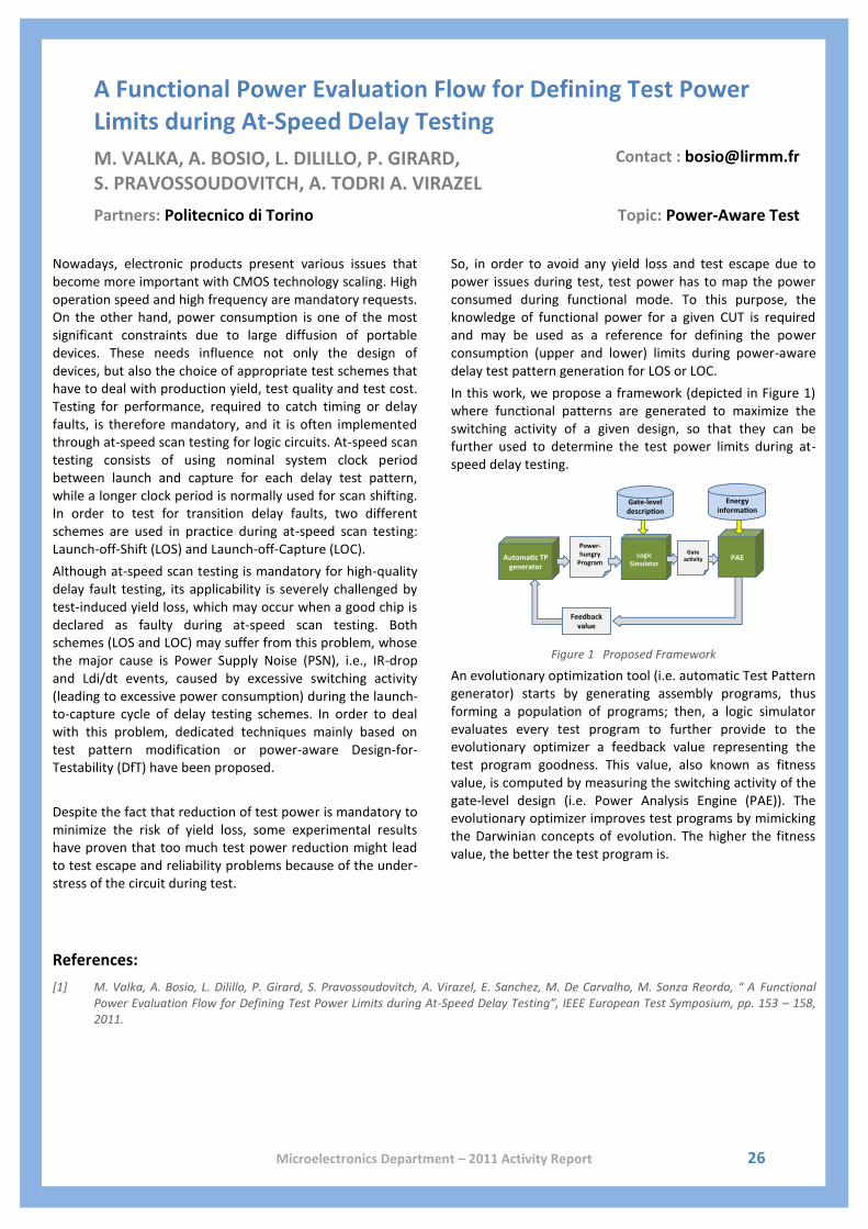
In this work, we propose a framework (depicted in Figure 1) where functional patterns are generated to maximize the switching activity of a given design, so that they can be further used to determine the test power limits during at-speed delay testing.
Figure 1 Proposed Framework
An evolutionary optimization tool (i.e. automatic Test Pattern generator) starts by generating assembly programs, thus forming a population of programs; then, a logic simulator evaluates every test program to further provide to the evolutionary optimizer a feedback value representing the test program goodness. This value, also known as fitness value, is computed by measuring the switching activity of the gate-level design (i.e. Power Analysis Engine (PAE)). The evolutionary optimizer improves test programs by mimicking the Darwinian concepts of evolution. The higher the fitness value, the better the test program is.
References:
[1] M. Valka, A. Bosio, L. Dilillo, P. Girard, S. Pravossoudovitch, A. Virazel, E. Sanchez, M. De Carvalho, M. Sonza Reorda, “ A Functional Power Evaluation Flow for Defining Test Power Limits during At-Speed Delay Testing”, IEEE European Test Symposium, pp. 153 – 158, 2011.

Microelectronics Department – 2011 Activity Report 27
Power Optimization of Transition Fault Test Vectors for At-Speed LOS Testing
F.WU, L. DILILLO, A. BOSIO, P. GIRARD, S. PRAVOSSOUDOVITCH, A. VIRAZEL
Contact : [email protected]
Partners: Catrene TOETS Topic: Power-Aware Test
Nowadays, at-speed scan testing is mandatory for performance verification. In this context, two main test schemes targeting delay faults are predominant: LOC (Launch-Off-Capture) and LOS (Launch-Off-Shift). Although LOC testing has been more widely investigated so far, LOS testing is now used in practice in industry and needs to be improved.
In this context, our goal has been to accurately evaluate peak and average power consumption during LOS testing, so as to propose effective techniques to generate power-aware tests. For this purpose, we proposed a test flow, shown in Figure 1, and performed a detailed analysis of LOC and LOS test schemes in terms of Transition Fault Coverage (TFC) and power consumption. The results achieved lead to the following conclusions: a) LOS performs better than LOC in terms of TFC and test length b) LOS peak power is significantly higher than LOC peak power during the Launch-to-Capture cycle.
Figure 1: Transition Fault and Test Power Estimation Flow
Consequently, LOS shows potential to be widespread used, provided that power consumption can be reduced or, better, mapped to the functional power. Targeting the functional power reduces yield loss due to over-stress and test escape due to under-test. In this work, we proposed a power-aware test pattern generation flow for LOS testing, shown in Figure 2. The goal is to obtain a final test set with peak power consumption as close as possible to the functional power consumption. The novelty of the proposed approach is twofold: (i) a test relaxation mechanism is used to identify don’t-care bits in a given test set, avoiding any loss in TFC and not increasing test length compared to conventional ATPG; (ii) X-filling is performed to tune the power consumption during the launch-to-capture cycle and thus map test peak power to functional peak power.
Figure 2: Power-aware test pattern generation flow
Experiments have been performed on ITC’99 circuits synthesized in a 65nm technology. The maximum peak power reduction achieved was about 50%. For large circuits, the average reduction was about 40% with 0-filling and Adjacent-filling, and 30% with 1-filling. In all cases, the combined use of these X-filling options with the conventional random filling option allows to obtain test patterns with a test power mapping functional power consumption.
References:
[1] F. Wu, L. Dilillo, A. Bosio, P. Girard, S. Pravossoudovitch, A. Virazel, M. Tehranipoor, K. Miyase, X. Wen, N. Ahmed, “Power Reduction Through X-filling of Transition Fault Test Vectors for LOS Testing”, IEEE International Conference on Design & Test of Integrated Systems, Athens, Greece, April, 2011
[2] K. Miyase, Y. Uchinodan, K. Enokimoto, Y. Yamato, X. Wen, S. Kajihara, F. Wu, L. Dilillo, A. Bosio, P. Girard, A. Virazel, “Effective Launch-to-Capture Power Reduction for LOS Scheme with Adjacent-Probability-Based X-Filling”, IEEE Asian Test Symposium, New Delhi, India, November, 2011

Microelectronics Department – 2011 Activity Report 28
Addressing Power and Thermal Issues During Test of Three-Dimensional ICs
C. METZLER, A. TODRI, A. BOSIO, L. DILILLO, P. GIRARD, A. VIRAZEL
Contact : [email protected]
Topic: TSV failure mechanisms, fault modeling
Three-dimensional integration is a fast emerging technology that enables multilayered circuit implementation. Through-Silicon-Vias (TSVs) provide short and fast interconnects between tiers and depending on the fabrication orientation they can connect: (i) face-to-face, (ii) face-to-back, (iii) back-to-face, and (iv) back-to-back between any two adjacent tiers. Manufacturing advancements have led to fine pitch TSVs and thinned silicon for die stacking. Depending on the 3D processing technology, multi-tier stacking can be performed on chip to chip, chip to wafer or wafer to wafer. Recent advancement on TSV development have led to production of TSVs in different ranges of dimensions.
Despite the manufacturing advancements, 3D integration is still immature. The multitude of manufacturing steps pre and post bond can introduce a lot of undesirable effects that can alter TSV performance or even cause such defects that can lead to TSV failure. Defects are physical aberrations due to partial or porous metal lines. Depending on the process sequence and 3D integration schemes (via last, first or middle) TSV fabrication process includes the following steps: TSV drilling, deposition of isolation and seed layer, filling (electroplating metal), wafer thinning, wafer planarization and bumping. TSVs are usually made of copper, and the process of electroplating the metal is likely to cause resistive opens where TSV channel is not completely filled or partly broken. This is also portrayed in Fig. 1a and Fig. 1b. A broken TSV can cause discontinuity on a signal line that may affect the chip latency or even completely interrupt the electrical connection between two nodes and causing a strong open.
However, open defects can also still connect the signal line’s two end points, but only weakly or referred to as a weak open. Weak open introduces a higher than expected but finite resistance on the TSVs, which lets the circuit to function but with degraded performance in the form of signal delay. Thus, it is imperative to ensure robustness and resiliency of TSVs for reliable operation of 3D ICs. In addition, it is important to detect chips with resistive open defects early on before shipping to maintain product reliability. In this work, we examine failure mechanisms on TSVs by employing models as shown in Fig. 1c and propose appropriate fault models. Additionally, dedicated test techniques are investigated for capturing open defect TSVs.
(c)
Figure 1. Illustration of resistive open defects in TSVs, (a) open defect, (b) resistive defect, and (c) TSV model.
References:
[1] C. Metzler, A. Todri, A. Bosio, L. Dilillo, P. Girard, A. Virazel, “Resistive-Open Defect Analysis for Through-Silicon-Vias,” accepted at IEEE European Test Symposium, 2012.
[2] C. Metzler, A. Todri, A. Bosio, L. Dilillo, P. Girard, A. Virazel, “Physical Characterization of Resistive-Open Defect on Through-Silicon-Vias,” submitted to IEEE Transactions on Computer Aided Design (TCAD), Special Section on 3D, 2012.
Insulator
Insulator
Layer
(SiO2)
Si Substrate
Break (Open Defect)
NMOS
PolySi
n+ n+
Metal Layer
T
S
V
Insulator
Insulator
Layer
(SiO2)
Si Substrate
Impurity (Resistive Defect)
NMOS
PolySi
n+ n+
Metal Layer
T
S
V
(a) (b)
Microelectronics Department – 2011 Activity Report 29
Modeling and Test of the ATMEL TSTAC™ eFlash Memory Technology
P.-D. MAUROUX, A. VIRAZEL, A. BOSIO, L. DILILLO, P.GIRARD, S. PRAVOSSOUDOVITCH
Contact : [email protected]
Partners: ATMEL Topic: NV-Memory, Flash, Memory testing
The increased usage of portable electronic devices such as mobile phones and digital camera produces a high demand for Flash memories. Flash memories are non-volatile memories that allow programming and erasing memory data electronically. The mainstream operation is based on the floating-gate concept in which charges can be stored and removed. Its low-power consumption and high integration density make it popular for portable devices.
The high integration density of eFlash memories and their particular manufacturing process steps make them prone to defects. Moreover, as high electric field is required to support its various operations, eFlash may be subject to complex disturbance phenomena.
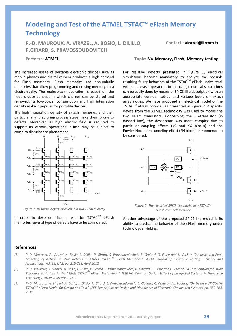
WL3
SG2
SG1
BL0
Vss
BL1
FGt30 FGt31
BL2 BL3
FGt32 FGt33
Vbulk
WL0 FGt00 FGt01 FGt02 FGt03
WL1 FGt10 FGt11 FGt12 FGt13
WL2 FGt20 FGt21 FGt22 FGt23
Df3
Df4
Df1
Df2
Df5
Df6
Df8
Df7
Df9
Figure 1: Resistive defect location in a 4x4 TSTAC™ array
In order to develop efficient tests for TSTACTM
eFlash memories, several type of defects have to be considered.
For resistive defects presented in Figure 1, electrical simulations become mandatory to analyze the possible resulting faulty behaviors of the TSTAC
TM eFlash under read,
write and erase operations In this case, electrical simulations can be easily done by means of SPICE-like description with an appropriate core-cell set-up and voltage levels on eFlash array nodes. We have proposed an electrical model of the TSTAC
TM eFlash core-cell as presented in Figure 2. A specific
device from the ATMEL technology was used to model the two select transistors. Concerning the FG-transistor (in dashed line), the description was more complex due to particular coupling effects (KC and KG blocks) and the Fowler-Nordheim tunneling effect (FN block) phenomenon to be considered.
FN
KC
KG +
+ + WL
SG2
SG1
BL
Vbulk
Vss
CTOT
Vchan
Vfg
Figure 2: The electrical SPICE-like model of a TSTAC™
eFlash core-cell memory
Another advantage of the proposed SPICE-like model is its ability to predict the behavior of the eFlash memory under technology shrinking.
References:
[1] P.-D. Mauroux, A. Virazel, A. Bosio, L. Dilillo, P. Girard, S. Pravossoudovitch, B. Godard, G. Feste and L. Vachez, “Analysis and Fault Modeling of Actual Resistive Defects in ATMEL TSTAC
TM eFlash Memories”, JETTA Journal of Electronic Testing - Theory and
Applications, Vol. 28, N° 2, pp. 215-228, April 2012.
[2] P.-D. Mauroux, A. Virazel, A. Bosio, L. Dilillo, P. Girard, S. Pravossoudovitch, B. Godard, G. Feste and L. Vachez, “A Test Solution for Oxide Thickness Variations in the ATMEL TSTAC
TM eFlash Technology”, IEEE Int. Conf. on Design & Test of Integrated Systems in Nanoscale
Technology, Athens, Greece, 2011.
[3] P.-D. Mauroux, A. Virazel, A. Bosio, L. Dilillo, P. Girard, S. Pravossoudovitch, B. Godard, G. Feste and L. Vachez, “On Using a SPICE-Like TSTAC
TM eFlash Model for Design and Test”, IEEE Symposium on Design and Diagnostics of Electronic Circuits and Systems, pp. 359-364,
2011.

Microelectronics Department – 2011 Activity Report 30
Test and Reliability of SRAM Memories
R. ALVES FONSECA, L. DILILLO, A. BOSIO, P. GIRARD, S. PRAVOSSOUDOVITCH, A. TODRI, A. VIRAZEL
Contact : [email protected]
Partners: Catrene TOETS / Intel Mobile Communications Topic: Memory Test
Nowadays, embedded memories are made with the fastest technologies and are among the most important components in complex systems. Within SoCs, memory devices are the most diffuse components, accounting for up to 90% of the chip area. Among the different embedded memory types, SRAMs are one of the most common and are of crucial importance in modern electronic systems.
The SRAM bit-cell transistors are often designed using the minimal dimensions of the technology node. As a consequence, SRAMs are more sensitive to new physical phenomena that occur in these technologies.
Our work on SRAMs can be divided in five main branches. Some branches are devoted to improve the post-production test process. We work also with characterization and new techniques of SRAM repair. Figure 1 shows a simplified scheme that allows us to visualize how each branch of our work is placed in the context of the SRAM Test and Reliability topic. The five branches are named:
1. Resistive-bridging Analysis
2. Stress Conditions
3. Statistical Simulation
4. Variability Characterization
5. Repair Techniques
The first branch, Resistive-bridging Analysis, is an historical topic of our research group. This work completes a series of studies on resistive defect insertion on the SRAM design. In the branch Stress Conditions, we propose methodology to improve the detection of non-deterministic faults during post production test.
We take into account physical phenomena that occur in modern CMOS fabrication process. This methodology is based on statistical simulations and requires simulations with extreme accuracy. A study on statistical simulation methods was then proposed, in order to achieve the accuracy requirements for SRAM bit-cell statistical simulation.
Figure 1: SRAM Test and Reliability Overview
These three branches contribute to the development of more efficient test strategies. Branch number 3, Statistical Simulation, is also related to the design of SRAM bit-cells, since we proposed a method that is suitable to be used in optimization problems, due to its high efficiency.
In branch number 4, Variability Characterization, we work with silicon measurements to gather physical information that will be further used on the test development and on SRAM design activities. Thanks to the collaboration with Intel Mobile Communications, we have access to measurements performed on latest technology test chips. Finally, in our branch Repair Techniques, we work on the development of new techniques of SRAM repair. We propose an innovative fault tolerance technique that does not use traditional redundant parts, reducing area and improving timing performance.
References:
[1] “Impact of Resistive-Bridging Defects in SRAM at Different Technology Nodes” in press, Journal of Electronic Testing: Theory and Applications (JETTA), DOI: 10.1007/s10836-012-5291-6, 2012
[2] “Variability Analysis of an SRAM Test Chip,” submitted to Elsevier Journal of Microelectronics on Dec 2011
[3] “Setting Stress Conditions for Improving SRAM Test Efficiency” submitted to IEEE Transaction on Very Large scale Integration Systems, Feb, 2012
[4] “On Using Address Scrambling to Implement Defect Toler-ance in SRAMs”, IEEE Int. Test Conference 2011.

Microelectronics Department – 2011 Activity Report 31
Test of Low Power SRAM Memories
L. ZORDAN, A. BOSIO, L. DILILLO, P. GIRARD, S. PRAVOSSOUDOVITCH, A. TODRI, A. VIRAZEL
Contact : [email protected]
Partners: Intel Mobile Communications Topic: Test, Low-Power, SRAMs
With the growing demand of hand-held devices, power dissipation has emerged as a major design concern. Simultaneously, technology scaling is shrinking device features as well as lowering the supply and threshold voltages, which cause a significant increase of leakage currents. Within System-On-Chips (SOCs), embedded memories are the densest components, hence arising as the main contributor to the overall SOC static power consumption.
Various techniques have been proposed to reduce the static power consumption of SRAMs. At architectural level, power gating provides several power modes for a given SRAM device by varying the supply voltage applied to the core-cells and peripheral circuitry. Power gating is generally implemented using power switches, which are controlled by a power mode control (PM control) logic.
The main goal of this work is to produce new generic and efficient test solutions for low power SRAMs. This is a new topic that offers research perspectives to a wide range of industrial applications. We started by studying the failure mechanisms that occur in nanometric technologies used for this type of memories, as well as their impact on current test solutions.
The SRAM used in this work embeds power switch (PS) blocks connected to the core-cell array and the peripheral circuitry. Such PS blocks are implemented through a network of PMOS transistors structured in N segments. Core-cell array PS segments have four transistors, whereas peripheral circuitry PS segments have two transistors. Signals connected to the gate of each PMOS in a segment are generated by the PM control logic, as shown in Figure 1, according to the power mode selected through primary inputs ("SLEEP" and "PWRON").
Signals Ctrl_CC0 to Ctrl_CC1 control the transistors of the core-cell array PS segments, while Ctrl_PC0 and Ctrl_PC1 control the transistors of the peripheral circuitry PS segments.
Figure 1. Power Mode control logic
Three power modes can be distinguished: (1) active mode, (2) deep-sleep mode, and (3) power-off mode. In active (ACT) mode, all PMOS transistors are activated. In this case, the whole memory is connected to the main supply rail VDD, which enables the SRAM to perform operations. In both deep-sleep (DS) and power-off (PO) modes, all PMOS transistors are deactivated, thus the SRAM is no longer connected to the main supply rail. In DS mode, a voltage regulation system generates a fixed voltage level Vreg, lower than the nominal VDD, to be provided to the core-cell array. The lower voltage Vreg still ensures data retention. In PO mode, the power supply voltage of the whole memory is shut off such that core-cells are no longer able to retain data.
We characterized the SRAM behavior in presence of resistive-open defects affecting the PM control logic primary outputs, as shown in Figure 1. We observed that all injected defects induce a delay on the activation of the PMOS they affect during wake-up (WU) phase from DS or PO mode to ACT mode. Def1 to Def3 and Def5 cause rush-in currents during WU phase, whereas Def6 leads to malfunctioning of operations executed after WU.
References:
[1] Zordan Y., Bosio A., Dilillo L., Girard P., Todri A., Virazel A., Badereddine N., “Failure Analysis and Test Solutions for Low-Power SRAMs”, IEEE Asian Test Symposium, pp. 459 – 460, 2011.
[2] Zordan Y., Bosio A., Dilillo L., Girard P., Todri A., Virazel A., Badereddine N., “Defect Analysis in Power Mode Control Logic of Low-Power SRAMs”, Accepted as poster at IEEE European Test Symposium, 2012
[3] Zordan Y., Bosio A., Dilillo L., Girard P., Todri A., Virazel A., Badereddine N., “Low-Power SRAMs Power Mode Control Logic: Failure Analysis and Test Solutions”, Submitted to IEEE International Test Conference, 2012

Microelectronics Department – 2011 Activity Report 32
Effects of High-Altitude Radiations on SRAMs
P. RECH, J.-M. GALLIERE, DILILLO, P. GIRARD, S. PRAVOSSOUDOVITCH
Contact : [email protected]
Partners: ANR Hamlet /CNES, IES, ATMEL Topic: Radiation effects on electronics
Radiation effects are a major concern for electronic systems in radiation harsh environments as the space and for common electronics at sea level. Impinging particles may corrupt bits stored in the memory array (Single Event Upset –SEU, or Multiple Bit Upsets –MBUs) or generate temporary voltage pulses in logic circuitry (Single Event Transients, SETs).
We focused our attention on the study of neutron effects on SRAMs. In particular, we studied the difference of errors occurrence between Static mode (data hold) and Dynamic mode (read/write accesses). For the former, write operations initialize the array, and read operations (performed after a predefined time, e.g. 1 hour) reveal the errors due to radiation. The dynamic mode consists of a specific sequence of operations (read/write) to be applied on the memory in order to stimulate (stress) both the cell array and the logic control circuitry.
We first performed SPICE simulations, which revealed that a traditional static test might underestimate the effective device sensitivity to neutrons, especially when the cells are affected by resistive-open defects [1]. Then, we developed a test platform composed of a large amount of memories to perform radiation tests in natural environment and by using accelerated neutron beams. This system is based on the principle of Built-On-Board-Self-Test (BOBST) that is capable of applying specific stressing sequences to the memories. We have also developed a software-based memory emulator that, connected to the BOBST, allows validating the test strategies before the actual experiments on field. The simulation experiment demonstrated that our system (BOBST based) is capable of detecting any radiation-induced error in the array as well as in the logic circuitry. Then, we performed accelerated experiment at TSL neutrons facility in Uppsala, Sweden [2].
We irradiated 4Mbits SRAMs with Quasi-Monoenergetic Neutron fluxes (QMN) of 114, 150, and 180MeV and with ANITA spectrum that mimics the amospheric environment. Fig. 1 represents the equipment used during the irradiation experiments. Results demonstrate how the stressed memory (dynamic mode) experiences a higher number or radiation-induced errors (higher cross section, Fig. 2). Next, we elaborated the experimental results to analyze the occurrence of multiple bit upsets, when the SRAM is in dynamic mode [3].
Figure 1: Experimental setup inside the Blue Hall of the TSL neutron
facility, Uppsala, Sweden.
0
1
2
3
4
5
6
7
114 150 180
Cro
ss S
ecti
on
[10
-13
cm2 ]
QMN energy [MeV]
static
stressed
Figure 2: Cross Sections of the 4Mbit SRAM for QMN fluxes obtained
with static test (solid line) and dynamic-stress test (dotted line).
References:
[1] “Impact of Resistive-Open Defects on SRAM Error Rate Induced by Alpha Particles and Neutrons”, IEEE Trans. on Nuclear Science, Volume: 58 , Issue: 3 , Part: 2 10.1109/TNS.2011.2123114, 2011 , Page(s): 855 - 861
[2] “Dynamic-Stress Neutrons Test of Commercial SRAMs”, 47th Nuclear and Space Radiation Effects Conference, Las Vegas, 2011
[3] “Multiple Bit Upsets on Two Commercial SRAMs under Dynamic-Stress”, IEEE Transaction on Nuclear Science, Issue: 99, Digital Object Identifier: 10.1109/TNS.2012.2187218, 2012

Microelectronics Department – 2011 Activity Report 33
Test and Reliability of Magnetic Random Access Memories
J. AZEVEDO, A. VIRAZEL, A. BOSIO, L. DILILLO, P.GIRARD, S. PRAVOSSOUDOVITCH, A. TODRI
Contact : [email protected]
Partners: ANR EMYR / Crocus, CEA Topic: MRAM, Memory testing
Magnetic Random Access Memory (MRAM) is an emerging technology with high data processing speed, low power consumption and high integration density compared with Flash memories. Moreover, these memories are non-volatile with fair processing speed and reasonable power consumption when compared to Static RAMs (SRAMs). Another important feature of MRAM is that the fabrication process is completely compatible to CMOS technology.
MRAMs are Spintronic devices that store data in Magnetic Tunnel Junctions (MTJs). A basic MTJ device is usually composed of two ferromagnetic (FM) layers separated by an insulating layer. One of the FM layers is pinned and acts as a reference layer. The other one is free and can be switched between, at least, two stable states. These states are parallel or anti-parallel with respect to the reference layer. When it is in the parallel state, the MTJ offers the minimum resistance (Rmin) while the maximum resistance (Rmax) is obtained when anti-parallel. The difference between Rmin and Rmax, quantified by the Tunnel Magneto Resistance (TMR), is high large to be sensed during the read operation.
“0”
“1”
Antiparallel, Rmax
Parallel, Rmin
FM
FMFM
FM
Figure 1: Basic MTJ device schematics in two stable states
A read operation consists in determining the MTJ’s magnetization state and can be performed by voltage or current sensing across the MTJ stack.
A write operation can be performed using magnetic fields or spin polarized current and depends on MRAM technologies: FIMS (Field Induced Magnetic Switching), Toggle Switching, TAS (Thermally Assisted Switching) and CIMS (Current Induced Magnetic Switching).
Thermally Assisted Switching is an alternative switching method for MRAMs proposed by Spintec and industrialized by Crocus Technology. TAS approach offers several advantages. The selectivity problem is reduced since only heated MTJs are able to switch and all other MTJs remain in their stable state as they remain below their blocking temperature.
This work is funded by the French national research agency under the framework of the ANR-10-SEGI-007 EMYR (Enhancement of MRAM Memory Yield and Reliability) project. In this project, our first goal was to analyzing the impact of resistive-open defects on the TAS-MRAM functioning. Electrical simulations have been performed using the MTJ model developed by Spintec that allows any read/write operation sequences. First results have already been achieved and hence published.
Figure 2: Resistive-open defect injection
References:
[1] J. Azevedo, A. Virazel, A. Bosio, L. Dilillo, P. Girard, A. Todri, G. Prenat, J. Alvarez-Herault, K. Mackay, “Impact of Resistive-Open Defects on the Heat Current of TAS-MRAM Architectures”, IEEE/ACM Design Automation and Test in Europe, Dresden, Germany, 2012.
[2] J. Azevedo, A. Virazel, A. Bosio, L. Dilillo, P. Girard, A. Todri, G. Prenat, J. Alvarez-Herault, K. Mackay, “Coupling-Based Resistive-Open Defects in TAS-MRAM Architectures”, to appear in IEEE European Test Symposium, Annecy, France, 2012.

Microelectronics Department – 2011 Activity Report 34
Test and Security
G. DI NATALE, M.L. FLOTTES, B. ROUZEYRE Contact : [email protected]
Topic: Hardware Security, Digital Test
Cryptographic algorithms are used to protect sensitive information when the communication medium is not secure. Unfortunately, the hardware implementation of these cryptographic algorithms allows secret key retrieval using different forms of attacks based on the observation of key-related information: physical information (side-channel attacks), faulty behaviors (fault-based attacks), or internal states (DFT-based attacks) for instance.
Since high quality product for secure applications is mandatory, the test of every component of the secure device must be performed. However, testing those devices faces a double dilemma: (i) how to test and, possibly, develop design-for-testability schemes providing high testability (high controllability and observability) while maintaining high security (no leakage), (ii) how to provide high security using dedicated design rules while maintaining high testability.
In the last 5 years we have proposed several techniques based either on the adaption of scan-based test to security constraints, or on the use of Built-In Self-Test architectures that allow high security while guaranteeing high levels of testability.
Scan chains, which aim to provide full controllability and observability of internal states, are against the principle of security that requires minimal controllability and observability.
Techniques to adapt scan chain-based designs with respect to security constraints are based on secure scan-chain controller, detection of unauthorized scan shift by test pattern watermarking, spy flip flops, scan enable tree inspection, and data confusion.
However, we have proved that crypto-devices are well suitable for this type of test. Indeed, from one side BIST approaches are effective for secure circuits since they do not rely on visible scan chains, thus preventing scan-based attacks. Moreover, it is shown how particular characteristics of crypto-devices allow very effective pseudo random tests.
We also analyze on-line BIST solutions to increase the fault tolerance of such devices, in particular against fault attacks. This attack is based on the intentional injection of faults (for instance by using a laser beam) into the system while an encryption occurs. By comparing the outputs of the circuits with and without the injection of the fault, it is possible to identify the secret key. To face this problem we analyze how to use error detection and correction codes as counter measure.
Since dedicated design for security techniques have been proposed so far (e.g., development of specific secure cell libraries, or implementation of extra functions for preventing the leakage of useful information for key identification), we eventually discuss perspectives and trends in digital testing of such dedicated components.
References:
[1] Fault Analysis in Cryptography, Chap. 6 "On Countermeasures Against Fault Attacks on Advanced Encryption Standard", K. Bousselam, G. DiNatale, M.L. Flottes, B. Rouzeyre. Spinger Series: Information Security and Cryptography, M. Joye; M. Tunstall, (Eds.), June 2012, ISBN 978-3-642-29655-0

Microelectronics Department – 2011 Activity Report 35
Scan-based Test and Security
J. DA ROLT, G. DI NATALE, ML. FLOTTES, B. ROUZEYRE Contact : [email protected]
Partners: PROSECURE/INVIA Topic: Digital Test and Security
Weaknesses of testable secure devices are questioned with respect to current Design for Testability strategies.
Insertion of scan chains is the most common technique to ensure full observability and controllability of sequential elements in an integrated circuit. However, when the chip deals with secret information, the scan chain can be used as back door for accessing secret (or hidden) information, and thus jeopardize the overall device security. Scan-based attacks assume single scan chain designs. However current very large designs and restrictions in terms of test costs require the implementation of many scan chains and additional test infrastructures for test data compression and/or masking unknown in the responses.
Recent publications claim that such advanced Design for Test (DfT) structures improve security, and that the previous published scan attacks are not applicable in this case. In [1] we introduce a new scan attack that allows to retrieve the secret key by observing the parity of the Advanced Encryption Standard round-register (observation after test response spatial compaction), showing that test response compaction does not provide a good level of security. This attack can be used in scenarios with single or multiple scan chains and with or without spatial compressors since the parity is observable in all these cases. We also propose two dedicated counter-measures in order to mask the round-register parity while being compatible with the design and test flow.
Figure 1. Advanced Dft Structures
A generic scan-based attack has finally been developed. It can be used for identifying [2] the position of the round-register bits in a scan-out bit-stream (i.e. in the scan chain), even in the case where they are not the only bits to switch when monitoring the AES input in the device (this condition was a prerequisite in the previous attacks).
We also addressed other DfT features such as partial scan, or structures inserted for masking unknown in the responses. We proved, by proposing a new attack [6], that such features, do not improve security, in spite of what's generally believed.
Finally, we developed a more general attack, called signature attack, able to tackle circuits implementing various ciphering algorithms, such as AES, DES, Khazad, ECC and RSA.
References:
[1] Jean Da Rolt, Giorgio Di Natale, Marie-Lise Flottes, Bruno Rouzeyre, "Scan attacks and counter-measures in presence of response compactors", IEEE European Test Symposium (ETS) 2011.
[2] Jean Da Rolt, Giorgio Di Natale, Marie-Lise Flottes, Bruno Rouzeyre, "New security threats against chips containing scan chain structures", IEEE International Symposium on Hardware-Oriented Security and Trust (HOST) 2011.
[3] Jean Da Rolt, Giorgio Di Natale, Marie-Lise Flottes, Bruno Rouzeyre, "New side-channel attack against scan chains", Groupe de Recherche SOC-SIP (GDR SOC-SIP) 2011.
[4] Jean Da Rolt, Giorgio Di Natale, Marie-Lise Flottes, Bruno Rouzeyre, "New side-channel attack against scan chains", Cryptographic Architectures Embedded in Reconfigurable Devices (CryptArchi) 2011.
[5] Jean Da Rolt, Giorgio Di Natale, Marie-Lise Flottes, Bruno Rouzeyre, "New scan attacks agains secure chips", Journées Nationales du Réseau Doctoral en Micro-nanoélectronique (JNRDM) 2011.
[6] Jean Da Rolt, Giorgio Di Natale, Marie-Lise Flottes, Bruno Rouzeyre, Are advanced DfT structures sufficient for
preventing scan-attacks ?", IEEE VLSI Test Symposium (VTS 2012), 2012
[7] Jean Da Rolt, Amitabh Das, Giorgio Di Natale, Marie-Lise Flottes, Bruno Rouzeyre, Ingrid Verbauwhede, “A New Scan Attack on RSA in Presence of Industrial Countermeasures", In third international Workshop on Constructive Side-Channel Analysis and Design (COSADE 2012), 2012
[8] Jean Da Rolt, Giorgio Di Natale, Marie-Lise Flottes, Bruno Rouzeyre, "On-Chip Test Comparison for Protecting Confidential Data in Secure ICs ", IEEE European Test Symposium (ETS) 2012.

Microelectronics Department – 2011 Activity Report 36
Low-Cost Testing of Analog/RF ICs using standard digital Automated Test Equipment (ATE)
F. AZAIS, L. LATORRE, N. POUS Contact : [email protected]
Partners: VERIGY Topic: Analog & Mixed Signal Testing
The production test of analog and RF devices is one of the major challenges for the development of modern microelectronic products. The test of these devices traditionally involves dedicated instruments to perform the acquisition or generation of analog signals. Compared to traditional digital resources, the cost of these instruments is extremely high.
Moreover analog/RF devices are often tested twice, at the wafer-level and again at the package-level. Implementing a quality test at wafer-level is extremely difficult due to probing issues, while the inability to perform multi-site testing due to a small count of available test resources decreases the throughput. Our objective is to propose a test solution applicable with low-cost test equipment that provides wafer-level test coverage and permits multi-site testing for analog/RF signals. The fundamental idea is to complement a standard digital ATE with signal processing techniques so that it permits the analysis of analog/RF signals. More precisely, the idea is to use the comparator of a standard digital ATE channel to sample the analog/RF signal. This comparator acts as a 1-bit digitizer and converts the amplitude and/or frequency information of the analog signal in timing information into the resulting bit stream. Post-processing algorithms can then be developed to retrieve this information.
Figure 1 illustrates the principle of data capture using a digital ATE channel. The Device Under Test (DUT) output is connected to the input of a digital channel that includes a programmable comparator, a latch, and a memory. The ATE provides a clock to the DUT to ensure synchronization. The channel comparator is used as a 1 bit digitizer and the resulting bit stream is stored in the ATE memory; data are then processed offline to retrieve the analog/RF signal characteristics.
Methods have been proposed that permits to estimate amplitude, frequency and phase of an analog signal from level-crossing events.
Dedicated algorithms have then been developed for the demodulation of elementary AM, PM and FM schemes [1], and validated both in simulation and experimentally with the setup shown in figure 2. More complex modulation schemes such as QAM that combines both amplitude and phase shift-keying have also been addressed [2].
Figure 1: Bloc diagram of the acquisition chain based on ATE digital
channel architecture.
Figure 2: Experimental setup for the signal acquisition and
reconstruction.
References:
[1] N Pous N., Azais F., Latorre L., Rivoir J., "A Level-Crossing Approach for the Analysis of RF Modulated Signals using only Digital Test Resources", Journal of Electronic Testing: Theory and Applications (JETTA), Vol 27, No. 3, pp 289-303, 2011 (doi: 10.1007/s10836-011-5222-y)
[2] N Pous N., Azais F., Latorre L., Confais G., Rivoir J., "Level-Crossing based QAM Demodulation for Low-Cost Analog/RF Testing", NEWCAS’11: IEEE New Circuits and Systems Conference, France, pp.309-312, 2011
CReconstuction
Algorithm
Analog/RF signal ATE
Memory
Pass/Fail
Regular Digital Pin Electronics
DUT/ATE SynchronisationATE Clock
«0011»
Comparator level
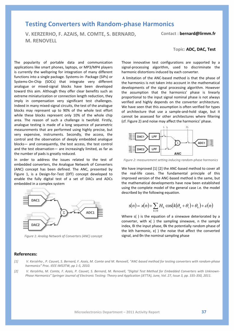
Microelectronics Department – 2011 Activity Report 37
Testing Converters with Random-phase Harmonics
V. KERZERHO, F. AZAIS, M. COMTE, S. BERNARD, M. RENOVELL
Contact : [email protected]
Topic: ADC, DAC, Test
The popularity of portable data and communication applications like smart phones, laptops, or MP3/MP4 players is currently the wellspring for integration of many different functions into a single package. Systems-in- Package (SiPs) or Systems-On-Chip (SOCs) that integrate very different analogue or mixed-signal blocks have been developed toward this aim. Although they offer clear benefits such as extreme miniaturization or connection length reduction, they imply in compensation very significant test challenges. Indeed in many mixed-signal circuits, the test of the analogue blocks may represent up to 90% of the whole test effort while these blocks represent only 10% of the whole chip area. The reason of such a challenge is twofold. Firstly, analogue testing is made of a long sequence of parametric measurements that are performed using highly precise, but very expensive, instruments. Secondly, the access, the control and the observation of deeply embedded analogue blocks— and consequently, the test access, the test control and the test observation— are increasingly limited, as far as the number of pads is greatly reduced.
In order to address the issues related to the test of embedded converters, the Analogue Network of Converters (ANC) concept has been defined. The ANC, presented by Figure 1, is a Design-for-Test (DfT) concept developed to enable the fully digital test of a set of DACs and ADCs embedded in a complex system
Figure 1: Analog Network of Converters (ANC) concept
Those innovative test configurations are supported by a signal-processing algorithm, used to discriminate the harmonic distortions induced by each converter.
A limitation of the ANC-based method is that the phase of the harmonics is not taken into account in the mathematical developments of the signal processing algorithm. However the assumption that the harmonics’ phase is linearly proportional to the input signal nominal phase is not always verified and highly depends on the converter architecture. We have seen that this assumption is often verified for types of architecture that use a sample-and-hold stage, but it cannot be assessed for other architectures where filtering (cf. Figure 2) and noise may affect the harmonics’ phase.
Figure 2: measurement setting inducing random-phase harmonics
We have improved [1] [2] the ANC-based method to cover all the real-life cases. The fundamental principle of this improved version of the ANC-based method is the same, but the mathematical developments have now been established using the complete model of the general case i.e. the model described by the following equation.
0
cosk
kink nkHnxns
Where s( ) is the equation of a sinewave deteriorated by a converter, with x( ) the sampling sinewave, n the sample index, θi the input phase, θk the potentially random phase of the kth harmonic, ε( ) the noise that affect the converted signal, and θn the nominal sampling phase
References:
[1] V. Kerzérho , P. Cauvet, S. Bernard, F. Azais, M. Comte and M. Renovell, “ANC-based method for testing converters with random-phase harmonics” Proc. IEEE IMS3TW, pp 1-5, 2010.
[2] V. Kerzérho, M. Comte, F. Azais, P. Cauvet, S. Bernard, M. Renovell, “Digital Test Method for Embedded Converters with Unknown-Phase Harmonics” Springer Journal of Electronic Testing: Theory and Application (JETTA), June, Vol. 27, Issue 3, pp. 335-350, 2011.

Microelectronics Department – 2011 Activity Report 38
Digital Post-Correction of Analog-to-Digital Converters (ADC)
S. BERNARD, F. AZAIS, M. COMTE, O. POTIN, V. KERZERHO, M. RENOVELL
Contact : [email protected]
Topic: ADC, design, correction
The semiconductor industry tends to constantly increase the performances of developed systems with an ever-shorter time-to-market. In this context, the conventional strategy for mixed-signal component design, which is based only on analog design effort, will no longer be suitable.
In order to combine ADC performance with short time to design, an alternative solution is the correction of Integral Non-Linearity (INL). As presented by Figure 1, the developed solution consists in using a post-processing correction table, also called Look-Up-Table (LUT).
Figure 1: LUT-based correction of ADC [1]
The efficiency of this technique is obviously based on the quality of the table used to correct the non-linearity. The table is usually computed using measurements of the Integral Non-Linearity (INL) of the ADC. INL is a conventional test parameter generally measured using a histogram-based method. This method has demonstrated its effectiveness for long periods but its main drawback is the huge amount of sampling required to compute the INL. As ADC resolution increases, test time also increases. With the rapid increase of ADC resolution, it is going to be difficult to implement this method. This is why we propose [1] alternative techniques to avoid the need for a histogram-based method to measure INL.
Based on our test vehicle, a 12-bit Folding-and-interpolating ADC, we have successfully validated a static correction table.
The study of the robustness [1] of the proposed technique has showed that the domain of validity is very large and covers the ADC application field. The robustness validation of the approach consisting in varying several functional (sampling frequency, converting frequency) and environmental (temperature) parameters has demonstrated that the correction is optimized when the operating conditions are the same as the conditions settled for the computation of the correction table.
Based on this observation, we proposed [2] a solution for “on-line” self-calibration of ADC with the on-chip capability of computing and filling the LUT (cf. Figure 2).
Figure 2: LUT-based self-correction of ADC [2]
By completing the LUT ‘in situ’, i.e. directly in the application, the corrected codes are computed according to the input signal dynamic, aging and environment conditions. Indeed the calibration is performed with an integrated adaptive signal generator providing an input signal tuned according to the application. The whole correction scheme is proved to be effective through extensive simulations.
Current developments focus on the minimization of the embedded resources used to compute the correction table. Software and hardware solutions are investigated in order to reduce the table’s size as much as the requirements on the performances of the embedded instrument.
References:
[1] V.Kerzérho, V.Fresnaud, D.Dallet, S.Bernard, L.Bossuet, “Fast Digital Post-processing Technique for INL Correction of ADC: Validation on a 12bit F&I ADC” IEEE Transactions on Instrumentation and Measurements, Vol.60, no.3, March 2011.
[2] S. Bernard, F. Azaïs, M. Comte, O. Potin, V. Kerzérho and M. Renovell, “Adaptive LUT-based System for In Situ ADC Auto-correction” Proc. IEEE IMS3TW, pp 1-6, 2010.
Microelectronics Department – 2011 Activity Report 39
Self-Calibration of NFC Antennas
F. AZAIS, S. BERNARD, Y. BERTRAND, M. COMTE, M. DIENG, V. KERZERHO, O. POTIN, M. RENOVELL
Contact : [email protected]
Partners: NXP Semiconductors Topic: RFID, NFC, self-adaptive systems
As a result of the evolution of different applications like access control, ticketing, payment and e-documents, the deployment of Near Field Communication (NFC) devices has been growing rapidly for several years. In particular, a variety of mobile phones equipped with NFC technology to enable such applications have emerged.
Due to the wide range of devices and applications, a predefinition of antenna geometry and corresponding electrical parameters is hardly possible. Each device shows different antenna physical characteristics; moreover each application for a given device shows different needs in terms of achievable distance… Therefore, each integrator associates the NFC IC with its own antenna for each device. Current NFC transmission modules require the antenna circuitry to be manually matched with the integrated circuit (IC) (see Application tuning block on fig. 1). This step is crucial to maximize the magnetic field and, therefore, to maximize the read range and the quality of the transmitted signal. According to the ISO 14443 standard, only well-matched reader devices fulfill the standard requirements and thus enable interoperability. Manual matching of the antenna characteristics is a rather lengthy and complicated procedure. Moreover, the matching can be done only once at the device design level, regardless of the communication mode (reader, card or peer to peer) and regardless of the secondary antenna influence on the primary antenna characteristics. Therefore, the manual matching is not optimal as far as the application and environment will detune the antenna in use.
Figure 1: NFC transmission module
To summarize, NFC technology is associated with an antenna that can have different physical characteristics (shape, size…) and that is influenced by environment and application. Our goal is to develop a technique to allow the NFC IC to adapt itself to these different antennas and environments in order to optimize its performances in terms of communication and power consumption.
The first step in our investigation is to study the physical phenomena associated with these antennas. The goal is to predict the variations of the antenna current and magnetic field by a mathematical model. The major difficulty of this exercise is to identify the effects associated with the coupling phenomena (mutual inductance) between different antennas when the NFC system communicates with another device (fig. 2). When the primary and secondary are coupled, that modifies the antenna characteristics based on the coupling coefficient that depends on the shapes, sizes, position, etc.
Figure 2: NFC communication
The second step of this study concerns the means to monitor and control the antenna performances via a self-calibration. The NFC circuitry should be able to adapt itself to its own antenna characteristics, which may differ from one application to another. The aim is to perform a self-diagnosis of the antenna characteristics and performances in its working environment using only the NFC circuit as interface (fig. 3).
Figure 3: Self calibration principle
Several assessment tools available in the core of the integrated circuit can be used to derive the maximum information. Analysis in these results is expected to monitor in real time the influence of the environmental area on the antenna characteristics and act on the internal components of the circuit as well as on a part of the application tuning circuit to improve performances for better communication.

Microelectronics Department – 2011 Activity Report 40
Alternate Testing of RF Integrated Circuits
H. AYARI, F. AZAIS, S. BERNARD, Y. BERTRAND, M. COMTE, V. KERZERHO, O. POTIN, M. RENOVELL
Contact : [email protected]
Partners: NXP Semiconductors Topic: RF, Analog & Mixed Signal Testing
The conventional approach for testing RF circuits is specification-based testing, which involves verifying sequentially all specification requirements that are promised in the data sheet. This approach is a long-time effective test approach but nowadays suffers from significant drawbacks. First, it requires generation and capture of test signals at the DUT operating frequency. As the operational frequencies of DUT are increasing, it becomes difficult to manage signal generation and capture using ATE. As a consequence, there is a need of expensive and specialized equipment. In addition, as conventional tests target several parameters, there is a need of several data captures and multiple test configurations. As a consequence, by adding settling time between each test and test application time, the whole test time becomes very long, and the test board very complex.
Another challenge regarding RF circuit testing is wafer-level testing. Indeed, the implementation of specification-based tests at wafer level is extremely difficult due to probing issues and high parasitic effects on the test interface. Moreover, multi-site testing is usually not an option due to the small count of available RF test resources, which decreases test throughput. Hence, the current practice is often to verify the device specifications only after packaging. The problem with this solution is that defective dies are identified late in the manufacturing flow, which leads to packaging loss and decreases the global yield of the process. In order to reduce production costs, there is therefore a need to develop test solutions applicable at wafer level, so that faulty circuits can be removed very early in the production flow. This is particularly important for dies designed to be integrated in Systems-In-Package (SIP).
In this context, a promising solution is to develop indirect test methods. Basically, it consists in using DUT signatures to non-conventional stimuli to predict the result of conventional tests. As illustrated in figure 1, the underlying idea is to learn during an initial phase the unknown dependency between simple measurements and conventional tests. This dependency can then be modeled through regression functions. During the testing phase, only the indirect measurements are performed and specifications are predicted using the regression model built in the learning phase.
Figure 1: Indirect RF IC test synopsis
Our work has been focused on two main directions. First, we have explored the implementation of the alternate test method based on DC measurements for RF circuits and we have proposed a methodology to select the most appropriate set of DC parameters. Results from two test vehicles (a LNA using electrical simulations and a PA using real production data) indicate that the proposed methodology allows precise estimation of the DUT performances while minimizing the number of DC measurements to be carried out.
Second, we have proposed a novel implementation of the alternate test strategy in order to improve confidence in alternate test predictions and to overcome the effect of limited training set sizes. The idea is to exploit model redundancy in order to identify, during the production testing phase, devices with suspect predictions; these devices are then are removed from the alternate test tier and directed to a second tier where further testing may apply. Examples of correlation plots obtained with this strategy are given in figure 2.
Figure 2: Examples of correlation plot between measured and predicted RF parameters after application of the two-tier alternate
test scheme using model redundancy

Microelectronics Department – 2011 Activity Report 41
Design & Test of MEMS

Microelectronics Department – 2011 Activity Report 42
Low-Cost Electrical Test & Calibration of MEMS Accelerometers
F. AZAIS, N. DUMAS, F. MAILLY, P. NOUET, A.A. REKIK Contact : [email protected]
Partners: ENIS, University of Sfax, Tunisia Topic: MEMS Testing
MEMS are multi-domain systems that find an increasing use in a number of applications. In particular, their deployment for high-volume and low-cost applications is expected to keep on growing. In this context, there is of great interest to reduce test and calibrations costs, which represent an important part of the total manufacturing costs. Indeed due to their multi-domain nature, they usually require the application of physical test stimuli to verify their specifications, necessitating specific and sophisticated test equipment much more expensive than a standard ATE. Moreover, MEMS devices are generally quite sensitive to manufacturing process variations and calibration is often required to achieve satisfactory yield.
An interesting approach is to develop electrical-only test and calibration techniques. A number of solutions have been proposed in the last decade for various types of MEMS such as accelerometers, magnetic field sensors, or pressure sensors. This project focuses on test and calibration of MEMS accelerometers’ sensitivity, which is the most challenging specification to measure without applying a calibrated acceleration. MEMS capacitive accelerometers were addressed in previous work; present activities concern MEMS convective accelerometers (see fig.1).
Figure 1: MEMS convective accelerometer.
First, a behavioral model that permits to handle faults related to manufacturing process has been developed, taking into account not only the classical CMOS process scattering but also imperfections related to the etching process. This model can be used in system-level simulation to evaluate different test and calibration strategies. Then, several electrical-only solutions have been investigated that exploit the correlation between device sensitivity and relative deviation of Wheatstone bridge equivalent impedance for different biasing conditions. In particular, an original scheme based on the adjustment of the power dissipated in the heating element has been developed. The test and calibration procedure relies only on impedance measurements, which can be performed with standard electrical test equipment. The procedure involves a preliminary step to reject devices affected by strong defects, and then an iterative search on the appropriated heater power level. A simple on-chip circuitry based on a pulse modulated generator is integrated within the circuit to permit the adjustment of the power level through digital programming (see fig.2).
Figure 2: Circuit implementation for electrical sensitivity calibration
using PDM generator.
References:
[1] A.A. Rekik, F. Azaïs, N. Dumas, F. Mailly, P. Nouet, "A behavioral model of MEMS convective accelerometers for the evaluation of design and calibration strategies at system level", J. of Electronic Testing: Theory & Applications (JETTA), Vol 27, No. 3, pp 411-423, 2011 (doi: 10.1007/s10836-011-5207-x)
[2] A.A. Rekik, B. Mezghani, F. Azaïs, N. Dumas, M. Masmoudi, F. Mailly, P. Nouet, "Investigation on the effect of geometrical dimensions on the conductive behaviour of a MEMS convective accelerometer", DTIP’11: IEEE Int’l Symp on Design Test Integration & Packaging of MEMS/MOEMS, France, pp.14-17, 2011
[3] A.A. Rekik, F. Azaïs, N. Dumas, F. Mailly, P. Nouet, "An Electrical Test Method for MEMS Convective Accelerometers: Development and Evaluation", DATE’11, France, pp.1-6, 2011
[4] A.A. Rekik, F. Azaïs, N. Dumas, F. Mailly, P. Nouet, "A MEMS convective accelerometer equipped with on-chip facilities for sensitivity electrical calibration", IMS3TW’11: IEEE Int’l Mixed-Signals, Sensors, and Systems Test Workshop, USA, pp.82-87, 2011
[5] A.A. Rekik, F. Azaïs, N. Dumas, F. Mailly, P. Nouet, "Test and Calibration of MEMS Convective Accelerometers with a Fully Electrical Setup", LATW’11: IEEE Latin American Test Workshop, Brazil, p.6, 2011
heater
detectors
sensing direction
without acceleration
under acceleration
RD1 RD2RH
RREF1 RREF2
VddN-bit register
N-bit ML-LFSR
Programming Word
Clock
N-bit comparator
Vdd
PDM generator

Microelectronics Department – 2011 Activity Report 43
Smart Wafer-level Packaging for Micro-Electro-Mechanical Systems
N. DUMAS, S. HACINE, L. LATORRE, F. MAILLY, P. NOUET Contact : [email protected]
Partners: ANR Midisppi, IMS, IEF, NXP, KFM Topic: Integrated Sensors
In mobile applications, Systems in Package (SiP) are commonly used. Figure 1 presents a SiP example from NXP Semiconductors where radio frequency (RF), analog, mixed signal and digital circuits are connected together by means of a silicon-based passive substrate. This substrate replaces the printed circuit board (PCB) and can be used to integrate RF passive components such as resistors or 3D-capacitors.
More recently, MEMS components have also been integrated within SiP. They need to be enclosed in a sealed cavity which quality has to be guaranteed in terms of pressure and humidity. For this purpose, environmental sensors (temperature, pressure and humidity sensors) may be integrated in the wafer-level packaging so that the final manufacturing test consists in checking the environmental parameters directly from those sensors. Moreover, during the life of the system, a periodic check of these sensors may be useful to be sure that MEMS performances are still within the specifications. At last, for a low deviation of the environmental parameters, and thus of system performances, sensor data can be used to calibrate the functional MEMS using an electronic loopback. Therefore, this smart wafer-level packaging will increase the manufacturing yield and the long-term stability of the system. Figure 2 shows a pressure sensor for such application. It is based on the Pirani gauge principle: the pressure-dependent heat losses of a self-heated microbridge through a surrounding gas. The sensor has been modeled and two different architectures have been investigated for electronic conditioning [1, 2]. For temperature sensing, an ultra low power sensor (Figure 3) has also been developed with a direct digital output [3].
Figure 1: SiP example with a cross section of a MEMS resonator
packaged at wafer-level.
Figure 2: SEM image of the Pirani gauge.
Figure 3: Temperature sensor
References:
[1] F. Mailly, N. Dumas, N. Pous, L. Latorre, O. Garel, E. Martincic, F. Verjus, C. Pellet, E. Dufour-Gergam, P. Nouet, Pirani Pressure Sensor for Smart Wafer-Level Packaging, Sens. Actuators A 156-1 (2009), p. 201-207
[2] O. Legendre, H. Mathias, E. Martincic, M. Zhang, J. Juillard, F. Mailly, High Resolution Micro-Pirani Pressure Sensor Gauge with Transient Response Processing, IEEE Sensors 2010, Waikoloa, Hawaii, November, 2010.
[3] S. Hacine, F. Mailly, N. Dumas, L. Latorre, P. Nouet, An Ultra Low Power Temperature Sensor For Smart Packaging Monitoring, Design, Test, Integration & Packaging of MEMS/MOEMS, Aix en Provence, France, 2011.
RF passive substrate
RF passive component
IC1
IC2
silicon cap
MEMS resonator
sensor conditioning
Pirani sensor
Act
ive
Bri
dg
e
R0+DR1
Vdd
R0+DR1
R0-DR2
R0-DR2
QD
fclk
MP1 MP2
MN1 MN2
Cint
Optional Comparator
Latch
Rfb
bitstream
Microelectronics Department – 2011 Activity Report 44
One-Chip Inertial Measurement Unit: Low-cost 3D Orientation Determination System
B. ALANDRY, F. MAILLY, L. LATORRE, P. NOUET Contact : [email protected]
Topic: Integrated Sensors
A multi-sensor platform has been developed to demonstrate our capabilities in sensor integration. Most of the know-how of the research team is illustrated in this project: sensor behavioral modeling, system-level simulation, front-end electronics, power management, wireless communication, embedded software, human machine interface...
The choice of a mature technology for the sensors makes the system suitable for low-end applications (e.g. consumer electronics) where the main trade-off concerns the power consumption, the cost and the size of the device. Our objective is thus to develop a low-cost, low-power, medium performance, highly integrated system.
The complete system is composed with three different sensors (a 2D in-plane accelerometer, a 1D out-of-plane accelerometer, a 2D in-plane magnetometer). All of them result from our previous research and have been extensively studied. Each sensor is connected to a specific front-end electronics that allow efficient offset compensation and cancellation schemes that are mandatory due to the low intrinsic performance of bare sensors. This architecture is completed with an embedded controller and a wireless communication module. The whole is powered by a battery. Details on most of these blocks are available elsewhere when browsing the research activity of our team.
SiP integration (figure 1) uses a passive substrate traditionally used to implement passive elements (R,L,C) and to connect them with one or several ICs to realize compact systems in a single package...
In our case, all sensors have been fabricated on the same technology and a CMOS electronic front-end has been added.
SoC integration (figure 2) is based on a CMOS 0.35 µm process that ensures a good trade-off between sensor cost and efficient electronic front-end. In both cases, electromechanical parts are released using wet etching as a self-aligned CMOS post-process.
Figure 1: Individual dies of the SiP IMU. (z-axis accelerometer die not shown).
Figure 2: One-Chip IMU includes three different sensors and the
front-end electronics on the same CMOS die.
References:
[1] Alandry B., Latorre L., Mailly F., Nouet P., “A CMOS-MEMS Inertial Measurement Unit”, IEEE Sensors Conference (SENSORS’10), Waikoloa, HI, USA, Nov. 1-4, 2010, pp. 1033-1036, ISBN 978-1-4244-8170-5
[2] Alandry, B.; Latorre, L.; Mailly, F.; Nouet, P., "A Fully Integrated Inertial Measurement Unit: Application to Attitude and Heading Determination", IEEE Sensors Journal, vol. 11, Issue 11, Nov. 2011, pp. 2852-2860, ISSN 1530-437X, DOI 10.1109/JSEN.2011.2170161.
Thermal Accelerometers (X,Y)
Magnetometers (X,Y)
Front-end electronics

Microelectronics Department – 2011 Activity Report 45
Smart High-Voltage Integrated Drivers for MEMS Switches with Diagnosis Capability
N. DUMAS, L. LATORRE, P. NOUET, C. TRIGONA Contact : [email protected]
Partners: ANR R3MEMS/Thalès Alénia Space, LAAS Topic: MEMS Interfaces
This study is part of a project that target the design of reflect array antennas for telecom applications. In this application, thousands of MEMS switches are embedded into RF cells to open or short RF paths so that a continuous phase shift is achieved between incident and reflected waves. Because a huge quantity of MEMS is used in a small surface the control and driving circuitry must be integrated close to the active area and a control architecture based on high-voltage ASICS has been defined. As different switch configurations may achieve the same phase shift, the architecture features an intrinsic redundancy so that alternate RF path may be used if non-working MEMS are identified. This is the reason why we proposed a diagnosis circuitry. From a RF point of view, this diagnosis is non-invasive since RF paths are not altered in any manner. It is based on the monitoring of the actuation current and thus only concerns the actuation circuitry. The measure must be as insensitive as possible to the routing between the driver and the switch.
We have investigated simple and fully integrated solutions for measuring the capacitance variation during pull-in event. The first one is based on a single step actuation voltage and a time-based technique to discriminate actuation capacitance increase during pull-in from stray capacitance. The second one is based on a two step actuation voltage and a differential technique. Finally, the use of a ramp-shaped actuation voltage provides good results in detecting both pull-in and pull-off events.
Switches depicted in figure 1 are fabricated by a partner. The design of the drivers includes the switch modeling in Verilog-A language and co-simulation within Cadence®. Figure 2 shows the 2nd generation of drivers integrated using a 0.35µm 50V CMOS technology.
The measure in figure 3 shows the peak in actuation voltage related to the pull-in event, which is used to perform the diagnosis. All drivers have been experimentally validated on various switches.
Figure 1: Artist view of a MEMS electrostatic Switch.
Figure 2: HV ASIC with 42 electrostatic actuation channels and
diagnosis capability.
Figure 3: Detection of a MEMS Pull-in event.
References:
[1] Dumas N., Trigona C., Pons P., Latorre L., Nouet P., “Design of Smart Drivers for Electrostatic MEMS Switches”, Sensors & Actuators: A. Physical 167 (2011), pp. 422-432. DOI: 10.1016/j.sna.2011.01.024.
[2] Trigona, C.; Dumas, N.; Latorre, L.; Nouet, P., "A novel integrated solution for the control and diagnosis of electrostatic MEMS switches", Symposium on Design, Test, Integration and Packaging of MEMS/MOEMS (DTIP’2011), Aix-en-Provence, France, 11-13 May, 2011, pp. 315-319, ISBN 978-1-61284-905-8.
Ground Plane
Actuation Electrode
Cantilever(grounded)
Signal Plane
Dielectric Layer CRF
CAct
CP
0.5
0.55
0.6
0.65
0.7
0 5 10 15 20
VIa
ct (
V)
Time (ms)

Microelectronics Department – 2011 Activity Report 46
Integrated Spin-Valves for Bio-Systems and Current-Sensors
N. DUMAS, S. HACINE, F. MAILLY, L. LATORRE, P. NOUET Contact : [email protected]
Partners: ANR SPIN/CEA-LETI, CEA-LIST, 3D+ Topic: Integrated Sensors
Giant Magneto Resistive (GMR) effect discovery has paved the way for the application of spintronics science to new integrated circuits based on the spin of electrons. It had a great impact on data storage device. Another domain where GMR effect is expected to lead to significant advances is integrated magnetic field sensing through spin-valves. The LIRMM is involved in designing the adapted read-out electronic of the spin-valves for two applications. The first one concerns the integration of an array of very sensitive magnetic sensor for detecting specific particle in medical application. The second one aims the integration of current and monitoring systems with high insulation for fuel cells used in automotive for example.
A new patented structure [1] for resistive sensors has been adapted and designed for these two previously described applications. It will allow evaluating this alternative to the Wheatstone in real conditions. This solution, called active bridge, has been demonstrated to provide an advantage in terms of trade off between SNR and power consumption. It can be used in an open loop in order to directly provide a strongly amplified analogue signal. For better sensitivity control, an analogue or digital closed loop system are preferred.
For biochip application, the analogue feedback provides amplification with a simple operational amplifier (figure 1). This simple circuit provides the equivalent performance compared to a Wheatstone bridge followed an instrumentation amplifier.
Figure 1: Active bridge with analogue feedback for biochip.
For the current sensing application a digital feedback provides directly a digital output (see on figure 2). This work has been published in a workshop on new integrated circuits and systems [2]. We demonstrated that the proposed read out structure should be independent on the power supply voltage and the temperature. A study of the best digital solution to feedback the structure has also been conducted. Finally a chip (figure 3) with a SPI interface has been designed and fabricated and is currently under characterization.
Figure 2: Active bridge with digital feedback for current monitoring.
Figure 3: 32 channels current sensor CMOS ASIC with location to
integrate spin-valve GMR on chip 3.5mm×9.5mm.
References:
[1] E.M. Boujamaa, P. Nouet, F. Mailly et L. Latorre, « CIRCUIT FOR AMPLIFYING A SIGNAL REPRESENTING A VARIATION IN RESISTANCE OF A VARIABLE RESISTANCE AND CORRESPONDING CAPACITOR ». Patent. International Publication Number (PCT): WO/2010/001077 A2, 7 January 2010.
[2] N. Dumas, S. Hacine, F. Mailly, L. Latorre, P. Nouet, "A Tracking Converter for Resistive Sensors based on a Feedback Active Bridge", 9th International New Circuits and Systems Conference (NEWCAS), Bordeaux, France, 26-29 June 2011.
100Ω
T1
T2
T3
VCC
T4
100Ω
200Ω RGMR
Vout
VCC
+
-
Rfeedback = 2kΩ
RGMR RGMR
T1
T2
T3
T4
RGMRRGMR
VDDA
n-1
Digital block
CLK
Sign
T5
VDDA
Ib
n
VSSA
RST
OUT
Sign
2n
blsb
2
II
Microelectronics Department – 2011 Activity Report 47
Exploitation of NonLinear Dynamics to improve the Performance of Energy Harvesters
C. TRIGONA, N. DUMAS, F. MAILLY, L. LATORRE, P. NOUET Contact : [email protected]
Partners: DIEEI, University of Catania Topic: MEMS Design
This study is part of a research that target the exploitation of novel nonlinear MEMS mechanism for energy harvesting applications based on ambient vibrations. The increasing demand for completely self powered devices and autonomous sensor node has caused an increase of research into power harvesting devices in recent years. Energy harvesting can be obtained from different energy sources; in particular we focus on mechanical vibrations. A common approach is based on vibrating mechanical bodies that collect energy through the adoption of self-generating materials. This family of systems has a linear mass–spring damping behavior and shows good performance around its natural frequency. However, it is generally not suitable to harvest energy in a wide spectrum of frequencies as expected in the vast majority of cases. Indeed, when ambient vibrations are considered, energy is distributed over a wide range of frequencies. Furthermore, whenever vibrations have a low frequency component the implementation of an integrated energy harvesting device is challenging; in fact, large masses and devices would be needed to obtain resonances at low frequencies. The idea pursued here is to consider the nonlinear behavior of a bistable system to enhance device performances in terms of response to external vibrations.
The switching mechanism is based on a structure that oscillates around one of the two stable states (Fig.1) when the stimulus is not large enough to switch to the other stable state and that moves around the other stable state as soon as it is excited over the threshold (Fig.2). Compared to the classical linear approach, a response improvement can be demonstrated (Fig.3). Indeed, a wider spectrum appears as a consequence of the nonlinear term and a significant amount of energy is collected at low frequencies [1].
Figure 1: Nonlinear mechanism used to improve the performance of
and energy harvester
Figure 2: Experimental results - displacement of an integrated
cantilever excited through vibrations
Figure 3: Experimental results spectrum response
References:
[1] Trigona C., Dumas N., Latorre L., Andò B., Baglio S., Nouet P., "Exploiting Benefits of a Periodically-Forced Nonlinear Oscillator for Energy Harvesting from Ambient Vibrations", Procedia Engineering, vol. 25 (after Eurosensors XXV conference, Athens, Greece, Sept. 4-7), 2011, pp. 819-822, DOI 10.1016/j.proeng.2011.12.201.

Microelectronics Department – 2011 Activity Report 48
Low-Power Front-End for Resistive Sensors
S. HACINE, N. DUMAS, L. LATORRE, F. MAILLY, P. NOUET Contact : [email protected]
Topic: Integrated Sensors
Interest for cheap and low-power integrated sensors is constantly growing with the development of low-cost portable consumer products and Wireless Sensor Networks (WSN). The use of standard CMOS technology together with cheap wet-etching post-process enables the batch fabrication of monolithic multi-sensor circuits that include accelerometers, magnetometers, microphones, pressure sensors, and temperature sensors. The design of such low-cost multi-sensors system is limited by a set of fabrication constraints that makes the use of capacitive sensing very difficult if not impossible. Therefore, resistive sensing is generally considered using either the piezoresistivity of polysilicon for mechanical devices or the temperature dependence of integrated resistors for thermal applications (including thermal accelerometers).
Resistive sensing is commonly valued for its low cost and ease of implementation but suffers from poor performance regarding the power consumption and the signal-to-noise ratio. In this context, we have proposed and patented an innovative circuit for the conditioning of resistive sensors that addresses the above mentioned issues. This so-called “Active Bridge” (figure 1) structure aims at providing amplification and limited noise contribution while using the same current to bias both sensing elements and amplification circuitry.
The Active Bridge main features are a high gain and high output impedance at very low biasing current (typically in the µA range or below). The implementation of a feedback circuitry is necessary to address gain and process mismatch issues.
feedback schemes have been investigated in various applications (inertial sensing, magnetic sensing). A digital output, high-resolution, micro-power, temperature sensors based on complementary temperature coefficient of resistors in an Active Bridge has been also developed and characterized.
Figure 1: Architecture of the “Active Bridg”
Figure 2: CMOS Temperature sensor based on the Active Bridge
and polysilicon thermistors
References:
[1] Hacine, S.; El Khach, T.; Mailly, F.; Latorre, L.; Nouet, P., "A micro-power high-resolution ΣΔ CMOS temperature sensor", IEEE Sensors Conference, Limerick, Ireland, 28-31 Oct, 2011, pp. 1530-1533, ISBN 978-1-4244-9290-9, DOI 10.1109/ICSENS.2011.6127123.
[2] Hacine, S.; Mailly, F.; Dumas, N.; Latorre, L.; Nouet, P., "An ultra low power temperature sensor for smart packaging monitoring", Symposium on Design, Test, Integration and Packaging of MEMS/MOEMS (DTIP’2011), Aix-en-Provence, France, 11-13 May, 2011, pp. 320-323, ISBN 978-1-61284-905-8.
R0+DR1
Vdd
R0+DR1
R0-DR2
R0-DR2
Vout
MP1 MP2
MN1 MN2
𝑣𝑜𝑢𝑡 = −4𝑔𝑚 𝐼0 𝑟𝑑𝑠1 ∕∕ 𝑟𝑑𝑠2 ∆𝑅𝑒𝑓𝑓

Microelectronics Department – 2011 Activity Report 49
Adaptive Circuits & Systems

Microelectronics Department – 2011 Activity Report 50
Adaptation Techniques for Massively Parallel Multiprocessor Systems-on-Chip (MPSoCs)
G. SASSATELLI, P. BENOIT, L. TORRES, M. ROBERT, G. M. ALMEIDA, N. HEBERT, R. BUSSEUIL, L. OST
Contact : [email protected]
Partners: DIEEI, University of Catania Topic: MPSoCs
The exponentially increasing number of transistors that can be placed on an integrated circuit is permitted by the dropping of technology feature sizes. This trend plays an important role at the economic level, although the price per transistor is rapidly dropping the NRE (Nonrecurring Engineering) costs, and fixed manufacturing costs increase significantly. This pushes the profitability threshold to higher production volumes opening a new market for flexible circuits which can be reused for several product lines or generations and scalable systems which can be designed more rapidly in order to decrease the Time-to-Market. Moreover, at a technological point of view, current variability issues could be compensated by more flexible and scalable designs. In this context, Multiprocessor Systems-on-Chips (MPSoCs) are becoming an increasingly popular solution that combines flexibility of software along with potentially significant speedups.
These facts challenge the design techniques and methods that have been used for decades and push the community to research new approaches for achieving system adaptability and reliability (out of unreliable technology components). Since this work targets massively parallel on-chip Multiprocessor systems, scalability is a major concern in the approach. For this reason, we put focus on distributed memory machines and therefore choose a message passing programming model for it provides a natural mapping to such machines.
The ADAptive Computing group (ADAC) designed a system based on an array of compact general-purpose PEs interconnected through a NoC.
The architecture is a purely distributed memory system that is programmed using a simple message passing protocol. Contrary to MPI, processes must not be mapped to a given processor but shall freely move in the system according to user-definable policies that may aim at optimizing a given property in the system, such as performance or power consumption. Both hardware and software resources are intended to be minimalist for favoring compactness of processors and therefore encouraging massive parallelism. Figure 1 presents a structural view of the OpenScale architecture. Based on that template, a number of distributed adaptation techniques have been explored for addressing concerns such as reliability, energy efficiency, performance optimization or quality of service. Both software and hardware descriptions are open-source, available for download at ADAC group website: http://www.lirmm.fr/ADAC/
Figure 1 - Structural view of the OpenScale architecture
References:
[1] G.M. Almeida, R. Busseuil, L. Ost, F. Bruguier, G. Sassatelli, P. Benoit, L. Torres, M. Robert, «PI and PID Regulation Approaches for Performance- Constrained Adaptive Multiprocessor System-on-Chip », IEEE Embedded Systems Letters, vol. 3, Issue 3, pp.77-80, doi: 10.1109/LES.2011.2166373, ISSN 1943-0663.
[2] R. Busseuil, G. M. Almeida, L. Ost, F. Bruguier, G. Sassatelli, P. Benoit, M. Robert, L. Torres, «Open-Scale: A Scalable, Open-Source NoC-Based MPSoC for Design Space Exploration». IEEE ReConFig'10 : International Conference on ReConFigurable Computing and FPGAs, ISBN: 978-0-7695-4551-6, 30 november – 02 december 2011, Cancun, Mexico, pp. 1-6.
[3] G. M. Almeida, S. Varyani, R. Busseuil, G. Sassatelli, L. Torres, E. A. Carara, and F. G. Moraes. Evaluating the impact of task migration in multi-processor systems-on-chip. In 23rd Symposium on Integrated Circuits and Systems Design (SBCCI’2010), pages 73–78, São Paulo, Brazil, September 2010. ACM Computer Society.

Microelectronics Department – 2011 Activity Report 51
Distributed Mechanisms for Adaptive Architecture Control
I. MANSOURI (CEA LETI), P. BENOIT,L. TORRES, F. CLERMIDY (CEA LETI)
Contact : [email protected]
Partners: ANR ADAM / CEA LETI Topic: MPSOC, Optimization
In 2008, the International Technology Roadmap for Semiconductors (ITRS) predicted that the number of processing cores in SoC (System on Chip) for consumer portable systems will increase, reaching up to six hundred cores in the next 10 years. Such systems provide more functionality with potentially higher performance. In the other hand, their complexity underlines many challenges, such as power management
We address the energy management issue in multi- core architectures articulated around a Network-on- Chip (NoC) as illustrated in Fig.1, assuming distributed sensors to collect the power consumption of each core, and actuators to adapt the voltage and frequency (DVFS) of each Processing Element (PE).
Considering multi-core architectures, the challenge is to go towards a scalable scheme of power management, where centralized control approaches are no more possible as it was demonstrated in [3]. Our focus is on a run-time distributed approach.
Figure 1: Noc-based System-on-Chip
A distributed scheme consists of a set of control loops attached to each PE, which operates independently but in a coordinated manner to assign the needed frequency for each core when applications constraints vary.
An existing controller inspired by game theory concepts, aims at modeling PEs as independent players, which can adjust their local frequencies via an in situ DVFS engine. We proposed Hardware/Software implementations of this technique and we evaluate induced overheads [2] in terms of area and latency.
While implementation results are promising, some problems related to the equilibrium stability and communications load were consequent. As alternative, we used consensus-based algorithms with limited neighborhood. Each PE operates with its nearby neighbors to reach an overall global “consensus” on the optimal settings corresponding to a given application. Depending on applied constraints, energy gains reach 46% compared to a worst-case static configuration as shown in Fig.2 [1].
Our current work includes the integration of some digital activity sensors in our control scheme, in order to feed our algorithm with accurate estimation of the system whole consumption.
Figure 2: Energy savings for different application constraints
References:
[1] Mansouri, I. et al, “A run-time distributed cooperative approach to optimize power consumption in MPSoCs,“ IEEE International SOC Conference, SOCC’10. Nevada, USA.
[2] Mansouri, I. et al., “An embedded Game Theoretic approach for energy management in NoC-based SoC, “ 2010 IEEE Computer Society Annual Symposium on VLSI, VLSI’10. Lixouri, Greece.
[3] Mansouri, I. et al, “On Energy Management in NoC-based System-on-Chip, “ Journal of Low Power Electronics, Vol. 6 N° 4 , December 2010.

Microelectronics Department – 2011 Activity Report 52
Variability and Aging Effects Characterization for Self-Adaptive System-On-Chip on FPGAs
F. BRUGUIER, P. BENOIT, L. TORRES Contact : [email protected]
Topic: MPSOC Variability
Variability has become a major issue in the semiconductor market due to its impact on manufacturing yields, performance and power consumption. A fine management of these physical disparities is a key to success for more reliable technologies. Despite suffering from the same symptoms, FPGAs have great advantages over other circuits: the regularity and the reconfigurability. These fundamental characteristics offer the possibility to map the same design to different regions of the circuit.
In our work, we investigate the problems of variability and aging effects characterization in FPGAs. We provide a twofold method for variability compensation based on digital sensors used either at design-time or at run-time. Basically, it uses FPGA digital resources (LUTs and interconnects) to implement Hard Macro sensors.
The FPGA performance is first deeply analyzed off-line at a fine granularity by our dedicated monitors at design-time. In order to realize an accurate characterization of performances, an array of sensors covering the whole area is used. Sensor data are collected and analyzed to build a cartography (Figure 1) of the floorplan. Once the cartography of the FPGA is built, a placement strategy is performed, considering both the system and its run-time monitoring service.
Figure 1: FPGA cartography performed by Electromagnetic analysis
The second stage of the compensation flow is based on hardware run-time monitoring. The run-time system implemented in the FPGA is composed of a microprocessor, some peripherals, a Management Unit, a set of sensors and actuators. Our objective is to perform a dynamic compensation of system variations. For this purpose, a subset of digital sensors using the FPGA resources is implemented. Digital sensors measure performances; data monitoring are then collected and analyzed by a management unit. Based on the information available, this unit can adapt the system to the actual performances.
References:
[1] F. Bruguier, P. Benoit, P. Maurine, and L. Torres, “A New Process Characterization Method For FPGAs Based on Electromagnetic Analysis” 21st International Conference on Field Programmable Logic and Applications, Chania, Greece, 2011, pp. 20-23
[2] Bruguier F., Benoit P., Torres L., “Capteurs Numériques pour la Gestion de Variations sur Circuits Logiques Programmables”, JNRDM 2011, Paris, France
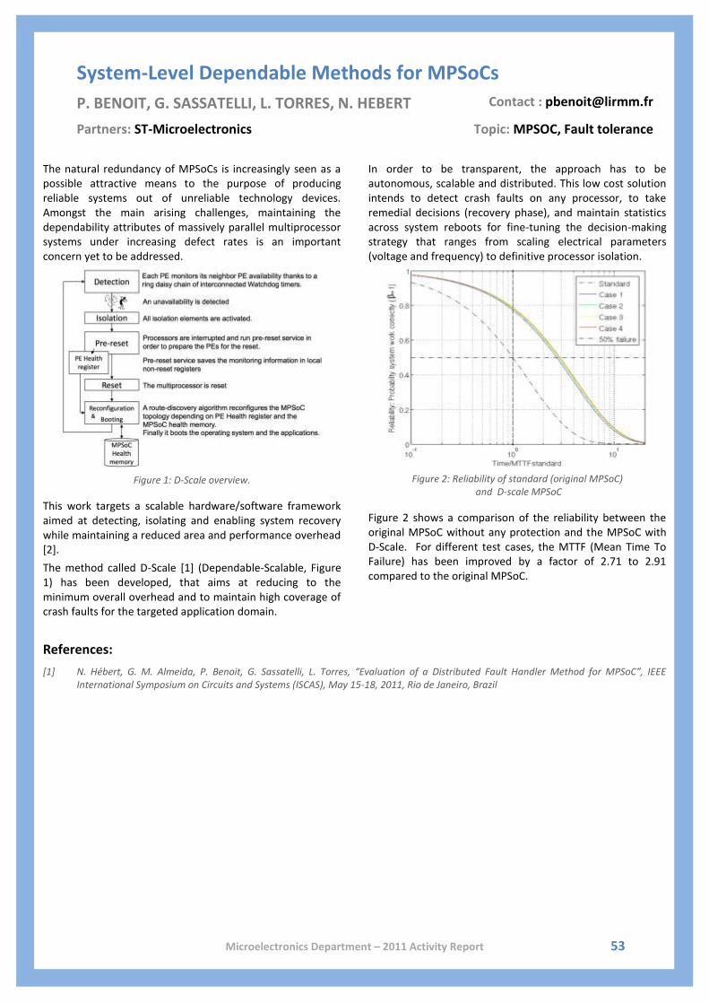
Microelectronics Department – 2011 Activity Report 53
System-Level Dependable Methods for MPSoCs
P. BENOIT, G. SASSATELLI, L. TORRES, N. HEBERT Contact : [email protected]
Partners: ST-Microelectronics Topic: MPSOC, Fault tolerance
The natural redundancy of MPSoCs is increasingly seen as a possible attractive means to the purpose of producing reliable systems out of unreliable technology devices. Amongst the main arising challenges, maintaining the dependability attributes of massively parallel multiprocessor systems under increasing defect rates is an important concern yet to be addressed.
Figure 1: D-Scale overview.
This work targets a scalable hardware/software framework aimed at detecting, isolating and enabling system recovery while maintaining a reduced area and performance overhead [2].
The method called D-Scale [1] (Dependable-Scalable, Figure 1) has been developed, that aims at reducing to the minimum overall overhead and to maintain high coverage of crash faults for the targeted application domain.
In order to be transparent, the approach has to be autonomous, scalable and distributed. This low cost solution intends to detect crash faults on any processor, to take remedial decisions (recovery phase), and maintain statistics across system reboots for fine-tuning the decision-making strategy that ranges from scaling electrical parameters (voltage and frequency) to definitive processor isolation.
Figure 2: Reliability of standard (original MPSoC)
and D-scale MPSoC
Figure 2 shows a comparison of the reliability between the original MPSoC without any protection and the MPSoC with D-Scale. For different test cases, the MTTF (Mean Time To Failure) has been improved by a factor of 2.71 to 2.91 compared to the original MPSoC.
References:
[1] N. Hébert, G. M. Almeida, P. Benoit, G. Sassatelli, L. Torres, “Evaluation of a Distributed Fault Handler Method for MPSoC”, IEEE International Symposium on Circuits and Systems (ISCAS), May 15-18, 2011, Rio de Janeiro, Brazil

Microelectronics Department – 2011 Activity Report 54
Securing an Embedded Linux Boot on FPGA: a Trusted Chain from Bitstream to OS
F. DEVIC, L. TORRES Contact : [email protected]
Partners: ANR SecReSoC / Netheos Topic: Hardware Security
With most of the FPGAs, the OS is stored into an external memory (usually Flash) and running on a processor embedded into the FPGA. We consider that FPGA embedded processor is able to process the OS update through, for instance, an insecure network. However, these features may give rise to security flaws affecting the system integrity or freshness. Spoofing or modifying data in order to introduce malicious code can alter integrity. In the same way, updated configuration (versioning) can be affected by replaying an old configuration in order to downgrade the system.
This work proposes a trusted computing mechanism taking into account the whole security chain from bitstream-to-kernel-boot ensuring, both hardware and software, integrity while preventing replay attacks into FPGA devices.
Figure 1 illustrates how to secure remote bitstream updates preventing replay attacks on FPGA embedding user non-volatile memory. The objective is to lock the FPGA to a dedicated bitstream version preventing downgrades. The bitstream version number (TAG) is stored in non-volatile user memory and can be incremented thanks to our protocol using secret keys [1].
Figure 2 describes the protected boot steps of the embedded Linux on generic FPGA. This boot mechanism precludes kernel modifications using Sha-256 hash function, prevents against replays attacks and supports updates [2]. It uses a flexibility improvement involving asymmetric cryptography that allows changing the kernel in external memory without changing the bitstream.
Figure 2: Boot with flexible integrity verification.
Figure 1: Anti-replay bitstream protection.
References:
[1] Devic F., Badrignans. B., Torres L., “Secure FPGA Configuration Architecture Preventing System Downgrade”, , FPL'10: 20th IEEE International Conference on Field Programmable Logic and Applications, Milano, Italia, September 2010, pp. 179-182
[2] Devic F., Badrignans. B., Torres L., “Boot of an Embedded Linux on FPGA”, RAW'11: workshop in IPDPS'11: 25th IEEE International Parallel & Distributed Processing Symposium, Anchorage (Alaska), USA, May 2011
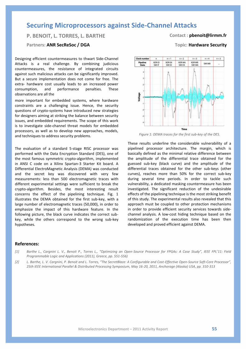
Microelectronics Department – 2011 Activity Report 55
Securing Microprocessors against Side-Channel Attacks
P. BENOIT, L. TORRES, L. BARTHE Contact : [email protected]
Partners: ANR SecReSoc / DGA Topic: Hardware Security
Designing efficient countermeasures to thwart Side-Channel Attacks is a real challenge. By combining judicious countermeasures, the resistance of integrated circuits against such malicious attacks can be significantly improved. But a secure implementation does not come for free. The extra- hardware cost usually leads to an increased power consumption, and performance penalties. These observations are all the
more important for embedded systems, where hardware constraints are a challenging issue. Hence, the security questions of crypto-systems have introduced new strategies for designers aiming at striking the balance between security issues, and embedded requirements. The scope of this work is to investigate side-channel threat models for embedded processors, as well as to develop new approaches, models, and techniques to address security problems.
The evaluation of a standard 5-stage RISC processor was performed with the Data Encryption Standard (DES), one of the most famous symmetric crypto-algorithm, implemented in ANSI C code on a Xilinx Spartan-3 Starter Kit board. A Differential ElectroMagnetic Analysis (DEMA) was conducted and the secret key was discovered with very few measurements: less than 500 electromagnetic traces with different experimental settings were sufficient to break the crypto-algorithm. Besides, the most interesting result concerns the effect of the pipelining technique. Fig. 1 illustrates the DEMA obtained for the first sub-key, with a large number of electromagnetic traces (50,000), in order to emphasize the impact of this hardware feature. In the following picture, the black curve indicates the correct sub-key, while the others correspond to the wrong sub-key hypotheses.
Figure 1: DEMA traces for the first sub-key of the DES.
These results underline the considerable vulnerability of a pipelined processor architecture. The margin, which is basically defined as the minimal relative difference between the amplitude of the differential trace obtained for the guessed sub-key (black curve) and the amplitude of the differential traces obtained for the other sub-keys (other curves), reaches more than 50% for the correct sub-key during several time periods. In order to tackle such vulnerability, a dedicated masking countermeasure has been investigated. The significant reduction of the undesirable effects of the pipelining technique is the most striking benefit of this study. The experimental results also revealed that this approach must be coupled to other protection mechanisms in order to provide efficient security services towards side-channel analysis. A low-cost hiding technique based on the randomization of the execution time has been then developed and proved efficient against DEMA.
References:
[1] Barthe L., Cargnini L. V., Benoit P., Torres L., “Optimizing an Open-Source Processor for FPGAs: A Case Study”, IEEE FPL’11: Field Programmable Logic and Applications (2011), Greece, pp. 551-556)
[2] L. Barthe, L. V. Cargnini, P. Benoit and L. Torres, “The SecretBlaze: A Configurable and Cost-Effective Open-Source Soft-Core Processor”, 25th IEEE International Parallel & Distributed Processing Symposium, May 16-20, 2011, Anchorage (Alaska) USA, pp. 310-313

Microelectronics Department – 2011 Activity Report 56
Magnetic-RAM-based memory hierarchy for microprocessors
L. V. CARGNINI, R. M. BRUM, G. SASSATELLI, L. TORRES Contact : [email protected]
Partners: ANR MARS / IEF, CEA, SPINTEC, EADS Topic: MRAM, Cache Memory
SRAM and DRAM have been the two main technologies employed in the design of on-chip processor memories. However, as the transistor dimensions continue to scale down, SRAM robustness and leakage power are becoming major obstacles. In the same way, the evolution of DRAM cells’ trench capacitors has been reported as a serious, possibly unworthy or unreachable challenge.
Magnetic Random Access Memory (MRAM) presents itself as an alternative for both technologies, due to its higher density, no leakage current when idle and, most notably, non-volatility. On the other hand, high write currents, higher write latency when compared to the contenders and the endurance of such devices are a concern.
We are evaluating the use of MRAM in Level-1 caches of microprocessors targeted for the embedded system domain. A preliminary study, based on data gathered from the SimpleScalar simulator running the set of benchmarks Mediabench 1, was presented in [1] and further developed in [2].
Figure 1: Same-area MRAM versus SRAM L1 Cache execution time
comparison, as show in [2].
Under the assumption that MRAM density can be four times higher than SRAM’s, it was shown that, for reasonably sized L1 caches, MRAM arrays cannot be directly used without significant performance decrease (Figure 1). A compensation mechanism must then be added to the memory hierarchy in order for the system to reach its expected operating frequency.
Two alternatives of compensation schemes are been developed: (1) write-buffers and (2) two-port MRAM memory arrays with a write queue. Write-buffers are commonly employed in write-through caches only, in an effort to minimize the memory bus traffic caused by this policy. In our case, however, write-buffers are used to mask the higher write delay while allowing the read operation to take place in a higher frequency.
They are meant to be of limited size and, whenever they are full, the processor should be able to stall its execution. In this case, the buffer is flushed into the higher memory level, allowing room for the coming write operations to be stored. Whenever the memory is idle, write operations can be committed to the actual cache.
Two-port MRAM arrays, in turn, allow write operations to take place simultaneously with read operations. Combined with a readable write queue (whose depth matches the write latency), this system can mask the write delay, as write operations can be performed in parallel. While this scheme requires a larger silicon footprint, it provides an ideal solution for the problem, in contrast with the write-buffer approach.
We now intend to study the feasibility of these two systems, and determine theoretical bounds for the parameters of both solutions.
References:
[1] Zhao, W.S.; Torres, L.; Cargnini, L.V.; Brum, R.M.; Guillemenet, Y.; Sassatelli, G.; Zhang, Y.; Lakys, Y.; Klein, J.-O.; Etiemble, D.; Revelosona, D.; Chappert, C.; “Embedded MRAM for high-speed computing”, 2011 IEEE/IFIP 19th International Conference on VLSI and System-on-Chip (VLSI-SoC 2011).
[2] Zhao, W.S.; Torres, L.; Cargnini, L.V.; Brum, R.M.; Zhang, Y.; Lakys, Y.; Guillemenet, Y.; Sassatelli, G.; Klein, J.-O.; Etiemble, D.; Revelosona, D.; Chappert, C.; “High Performance SoC Design using Magnetic Logic and Memory”, an extended version of the previous article to appear as a book chapter.
-100
-80
-60
-40
-20
0
20
1:4
2:8
4:1
6
8:3
2
16
:64
32
:12
8
64
:25
6
12
8:5
12
MR
AM
CP
I Pe
nal
ty (
%)
Cache Capacity - SRAM:MRAM (KB)
Worst Average Best

Microelectronics Department – 2011 Activity Report 57
Verification of taped-out magnetic shift registers and LUTs
R. M. BRUM, L. V. CARGNINI, G. SASSATELLI, L. TORRES Contact : [email protected]
Partners: ANR MARS / CEA, Menta S.A.S. Topic: MRAM, Non-volatile Logic
Magnetic Tunneling Junctions, or MTJs, are spintronic devices whose magnetic orientation can be modified to store data. From an electrical point of view, they are four-terminal devices, in which one pair of terminals presents either one of two pre-defined resistance values. The second pair allows us to program the resistance between the first two terminals.
These devices are the basic building blocks for the latest generation Magnetic RAMs. They can also be used to build combinational and sequential logic cells, or even CAMs (for Content-Addressable Memories) and LUTs.
During the course of the ANR projects CILOMAG and SPIN, our research group has designed a bank of non-volatile registers and small look-up tables (Chip 2), as well as a complete Magnetic FPGA (Chip 3) [1]. The prototypes were fabricated using a 130nm CMOS node (ST HCMOS9GP), on top of which the MTJ layers were added by CMP.
These circuits are composed both by a digital control and by analog circuitry, the latter being entirely handmade and verified separately during the design process.
In the current project, a methodology to properly simulate and verify their functionality in practice was developed. A standard FPGA is used to generate the input stimuli to the test chip (DUT). Its outputs are connected back to the FPGA, which can be easily monitored by signal probes such as ChipScope.
A mixed-signal simulator is employed to verify our testbed and the DUT itself. A fine-grain simulation of the analog part makes for accurate results, whereas a coarse-grain simulation of the control circuit reduces the runtime significantly.
We can also vary parameters such as the supply voltage and the actual junction size during the simulation. It is then possible to extract the sensitivity of the circuit to these parameters.
Our team is responsible for the verification of Chip 2. The verification process of the MFPGA (Chip 3), the most complex circuit designed in these projects, is being done in partnership with CEA and Menta S.A.S.
Figure 1: verification flow in two steps: simulation phase and the actual test, done by synthesizing the testbench to an FPGA.
References:
[1] Guillemenet, Y. ; Torres, L. ; Sassatelli, G. ; “Non-Volatile Run-Time FPGA structures using Thermally Assisted Switching MRAMs”, International Journal of Computers & Digital Techniques (IET-CDT 2010).
Netlistextraction
Full-customcircuit layouts
Full-custom circuit netlists
Stimuli generator
Digital circuitry description
Synthesis on FPGA
StimuliGenerator
(FPGA)
DUT(Chip)
Stimuli
Output
Mixed-signal simulation
Expected output
Chip output
Signals Monitor
(PC)
Verificationresults

Microelectronics Department – 2011 Activity Report 58
Power Management in embedded systems with performance constraints
Y AKGUL, D. PUSCHINI, S. LESECQ, P. BENOIT, L. TORRES Contact : [email protected]
Partners: CEA LETI Topic: System-on-Chip, power management
In embedded systems, the main issue is to strike the balance between performance and power consumption. The well-known Dynamic Voltage and Frequency Scaling (DVFS) technique allows decreasing power consumption when applications require less performance. DVFS is usually achieved by setting the supply voltage and the clock frequency to predefined values (so-called “Power Modes”, or PM) during given durations. Considering a given application composed by a set of tasks, with various performance constraints (defined for instance by the task deadline), it is possible to optimize performance vs. power consumption by adjusting the duration of each PM. This problem of power management is recast as a linear programming one and the computation of the duration spent in each power mode is obtained with a Simplex algorithm solution.
We assume a given processing element PE of a MPSOC or multicore system with different PMs. The main objective is to choose a sequence of PMs, and the duration of each PM, in order to minimize the total power consumption of a PE when N (≥ 2) power modes (PMs) are used. A PM is defined with the clock frequency F applied to the PE and the power consumption P associated to F (and to its related supply voltage Vdd), as depicted in Figure 1. Assuming that a PE has to run task T with a known deadline d, we consider a deterministic application so that task T requires NI clock cycles to be fully processed, including all possible memory accesses and specific functions. The mean frequency F required to execute the NI clock cycles on the deadline d is
dNIF /
In [1] an analytical study was presented with 3 PMs. We have proved that choosing the 2 PMs corresponding to the frequencies that frame the mean frequency defined above, does not always provide an optimal solution.
Our results show that for a given distribution of the power modes, a maximum improvement is reached for a particular workload. Moreover, it also shows that for a given workload, the 3rd power mode might be adjusted in order to improve the power consumption.
The case with N > 3 PMs must be studied in order to express the optimum solution in an analytical form, if possible. In this way, the optimization problem, solved with the Simplex algorithm in this work, will be solved through simple computations or through an adapted solving tool, possibly implemented in hardware. On the one hand, future works concern taking into account the switching time and power between PMs. On the other hand, providing a methodology to fix the distribution of the various power modes along [F1 , FN] and [P1, PN] will be studied in order to improve the power consumption of the VFI for a given range of workload.
Figure 1. N power modes (Fi; Pi) , i=1:N

Microelectronics Department – 2011 Activity Report 59
Biomedical Circuits and Systems

Microelectronics Department – 2011 Activity Report 60
Implantable Neural Stimulator: Output Stage Improvements
J. SALLES, S.BERNARD, G. CATHEBRAS, F. SOULIER Contact : [email protected]
Partners: FP7 TIME / Neuromedics Topic: Analog Design, Functional Electrical Stimulation (FES)
Functional Electrical Stimulation (FES) has been used for about 30 years in order to restore deficient physiological functions. At the beginning, only surface stimulation was possible and thus only used in a clinical context due to the low reliability of electrode placements. In the early eighties, implanted FES appeared through well-known applications: pacemaker, Brindley bladder control, cochlear implant, and more recently deep brain stimulation (DBS).
Currently, FES is the only way to restore motor function even though biological solutions are studied, but not yet successfully tested on humans. Few teams carry out researches on implanted FES and the functional results remain poor.
The team developed a microstimulator in 2006 and a prototype (ASIC) was fabricated. The microstimulator can be divided in to two main parts: a controller (digital) and an active part (analog). In the active part, the output stage gets its input current from an external DAC converter which set the maximum stimulation amplitude. This current is then distributed to a twelve-pole stimulating electrode. A pole can be set in four different states: anode, cathode (both current controlled), open (high impedance) or shunt (voltage-controlled). A digital block controls the evolution of the pole states and the ratio of the stimulation current on each pole.
Some faults were observed while carrying out the circuit characterization. These faults were of four main kinds:
• asymmetry between poles (up to 108 μA),
• input/output non-linearities (over 4 LSB),
• over-consumption on idle state,
• erratic level-shifter behavior.
Since 2006, some researchs and experiments were carried out and few subcircuits were developed to fully access its faults and correct them. Finally, a corrected version was designed in 2010. The new IC offers three structural modifications and better layout techniques to improve the stimulator characteristics. Some simulation results are presented in the following pictures. The fig. 1 shows an improvement of the symmetry between poles (down to 39 μA) while the fig. 2 highlights a non-linearity reduction to 0.66 LSB. The command structure was also modified to get rid of the over-consumption. Finally, the level-shifter parts were designed anew.
The corrected ASIC was manufactured on November 2010 and is now under test and characterization.
Figure 1: Simulated voltage/current characteristics of CAFE12
Figure 2: Simulated non-linearities of a typical electrode
(cathode in red and anode in black)

Microelectronics Department – 2011 Activity Report 61
Dependability of Medical Implanted Devices
F. LE FLOCH, G. BONTORIN, S. BERNARD, F. SOULIER, G. CATHEBRAS
Contact : [email protected]
Topic: Dependability
The FES (Functional Electrical Stimulation) implanted system may be hazardous for patient and the reliability and dependability of the system must be maximal. Unfortunately, the associated systems are more and more complex and the fact that their development needs very cross-disciplinary experts is not favorable to safety. Moreover, the direct adaptation of the existing dependability techniques from domains such as space or automotive is not suitable. Therefore, we have developed a strategy for risk management at system level for FES medical implant. The idea is to give a uniform framework where all possible hazards are highlighted and associated consequences are minimized.
The base of the proposed risk management method is an algorithm. This algorithm must be as simple as possible to achieve the best coverage of defective cases and propose the highest level of confidence and safety of the system (see figure 1).
The functional Analysis defines the system, its environment and its external limits. Then, we create specific expertise group defined according to their skills. Each working team will now write its own hazard’s analysis which draws up the full list. Once each working team has established its specific hazard’s analysis, it is then sent to the person in charge of the dependability study. The hazard chart has to be as exhaustive as possible. Afterwards, a global risk analysis will be conducted.
We associate to each hazard a probability of occurrence and a level of consequence. According to this classification, each working team will be asked to either decrease the probability of occurrence or the consequence of a risk with appropriate countermeasures. They will develop specific Built-In-Self- Test and Built-In-Self-Repair solutions of hazards that can occur in order to increase the dependability of the system. The dependability study has to be carried on over the entire life of the project, thanks to the experience feedback, the study can be completed and improved.
Figure 1: Algorithm of the system dependability management.
References:
[1] New Dependability Approach for Implanted Medical Devices, in: ICM'09: International Conference on Microelectronics, Marrakech (Morocco), 2009.
[2] Dependability for implanted medical devices, in: DECIDE'08: Second International Workshop on Dependable Circuit Design, Mexico, november 2008.
[3] Sûreté de fonctionnement pour les implants médicaux, in GDR SOC/SIP, 2009.
[4] Dependability: a challenge for electrical medical implant, in EMBS, 2010, Buenos Aires.

Microelectronics Department – 2011 Activity Report 62
Selective Electroneurogram Recording
O. ROSSEL, F. SOULIER, S. BERNARD, G. CATHEBRAS Contact : [email protected]
Partners: AXA, INSERM Topic: Nerve Model & Analog Signal Processing
In the context of FES, neural recording is one of the main issues, as the control requires information, carried on afferent peripherals nerve. Because specific informations are carried into different fascicles, we propose to realize a non-invasive and spatial-selective electrode. Last year, based on investigation on the topic of Extracellular Action Potentials (AP), we proposed a new tripoles design, were the tripolar output signal is the image of the activity on the close vicinity of this tripole, providing high spatial selectivity. We showed however, that this high spatial selectivity is achieved at the expense of signal amplitude. This first result jeopardizes the feasibility of this kind of electrode since the signal amplitude appears to be on the same range of the expected noise. First we propose to estimate the performance of the proposed electrode with a quantitative study of the electrode selectivity. Then, to conclude on the feasibility of this electrode, the SNR has to be determined. So with a more accurate model, we studied the sensitivity of the proposed tripole, allowing to determine precisely the amplitude level of the expected signal. Thus, the SNR can be estimated knowing the expected noise. In short the work of this year aims at characterizing the performances and evaluating the feasibility this new multi-contact cuff electrode.
Figure 1: Electrodes A and B have the same shape but differ on the
longitudinal inter-pole distance (de).
We proposed an electrode configuration inspired from the FINE electrode (figure 1) designed for the same purpose. The electrode is composed of many tripoles, placed around the nerve. This disposition is used for two electrodes, state-of-the-art electrode A and the proposed electrode B. The unique difference between both electrode reside on the longitudinal inter-pole distance de, which is respectively 5mm for the electrode A and 0.375mm for the electrode B.
The electrodes performances are evaluated based on simulations using a model of a nerve comprising multiple fascicles. We shows that activity of two fascicles separated by as little as 1mm can be distinguished for the proposed electrode B (for this distance SI for electrode B (SI≈0.9) is more than double that of electrode A (SI<0.4)). Where, the Selectivity Index (SI) quantifies the ability to record and distinguish between different active fascicles (0<SI<1). The proposed electrode B appears to be much more selective than the reference electrode A.
Using a more realistic model (in-Homogenous and anisotropic) we investigate the spatial properties of extracellular actions potentials (AP) and that of spatial properties of the filtering done by the proposed tripole. This allows us to represent the tripolar sensitivity (figure 2). This sensitivity represents the amplitude of the tripolar output signal for a single unit action potential. This figure shows that the classical tripole radius sensitivity is huge compare to that of the proposed electrode. This confirms the high spatial sensibility of the proposed tripole. We can also determine the expected amplitude, where the signal can reach 6µV.
Figure 2: Comparison between Tripoles sensitivity (tripole A on the
left, and B right) with the pic to pic amplitude of a single unit action potential.
References:
[1] O. Rossel, F. Soulier, J. Coulombe, S. Bernard, and G. Cathébras, Fascicle-selective multi-contact cuff electrod, in: EMBC'11: 33st Annual International Conference of the IEEE Engineering in Medicine and Biology Society, 2011
[2] O. Rossel, F. Soulier, S. Bernard, and G. Cathébras, Sensitivity of a Frequency-Selective Electrode based on Spatial Spectral Properties of the Extracellular AP of Myelinated Nerve Fibers, in: EMBC'11: 33st Annual International Conference of the IEEE Engineering in Medicine and Biology Society, 2011

Microelectronics Department – 2011 Activity Report 63
Continuous Intra Ocular Pressure Measurement for Glaucoma Diagnosis
S. BERNARD, F. SOULIER, O. POTIN Contact : [email protected]
Partners: MATEO / Ophtimalia, Institut de la Vision, ESIEE, CEA
Topic: Sensor, RF, Medical devices
Glaucoma being an ocular pathology and the second cause of blindness in people over the age of 50, the aging of the world population will lead to further increase the number of patients greatly visually impaired by this disease. In most cases, glaucoma is associated with an increase in Intra Ocular Pressure (IOP). In this work funded within the ANR-TecSan project MATEO, we are developing disposable eye lenses including a specific pressure sensor to measure IOP all day long. The instrumented lens will communicate by radio frequency to an electronic chip located on glasses arms and daily information would thus be available for ophthalmologists to improve diagnoses.
The system consists of a sensor implanted on a lens and an external reader on the glasses, see figure 1. The system is therefore based on inductive coupling between the coils L1 and L2 respectively representing the reader and the embedded sensor.
Figure 1: Principle of the wireless communication
(sensor in the lens and reader on glasses)
So any parameter variation on the lens induced by a mechanical deformation of the cornea will be converted into a frequency shift, detectable while measuring either the impedance magnitude or phase.
The challenges are multiple. Firstly, the sensor design must offer the maximum sensitivity due to the small deformation of the cornea (less than 3µm). Secondly, it should be coupled with the integrated antenna on a small transparent polymer lens.
Thirdly, electronics should deal with a composite signal degraded by strong interferences to extract data and provide a reliable and accurate IOP measurement. We proceed by modeling the complete system (see figure 2) from the mechanical deformation of the eye to the electrical measurement. This model permits to propose implementations of signal processing and high-level architecture of the active integrated circuit, under high constraints in terms of area overhead, power consumption, robustness, testability and safety. Moreover, we develop algorithms for measurement data extraction. Finally, a key point remains the integration of auto-test techniques to guarantee the reliability of the system. The aims are both to analyze the system before delivery and adapt it to environment variations by an auto-calibration process.
Figure 2: high-level model of the measurement system.
In parallel, first experimental results demonstrate the feasibility of the IOP measurement with the prototype sensor. We can observe on figure 3 that the impedance phase slightly changes while the IOP is increased by injecting fluid inside pig eyes on which the sensor is tested.
Figure 3: Measured phase vs frequency with IOP varying from 10 to
70mmHg.
References:
[1] Gaëlle Lissorgues, Lionel Rousseau, Patrick Poulichet, Laurie Valbin, Serge Picaud, Laurent Chicaud, Serge Bernard, Philippe Bergonzo, Francois Dedieuleveult and Philippe Auvray, “Continuous Intra Ocular Pressure Measurement Sensor for Glaucoma Diagnostic” WCB 2010, IFMBE Proceedings 31, pp. 1282–1285, 2010

Microelectronics Department – 2011 Activity Report 64
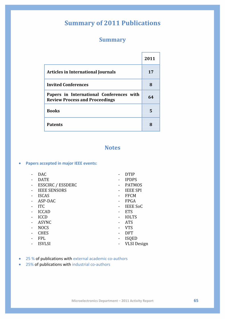
Microelectronics Department – 2011 Activity Report 65
Summary of 2011 Publications
Summary
2011
Articles in International Journals 17
Invited Conferences 8
Papers in International Conferences with Review Process and Proceedings
64
Books 5
Patents 8
Notes
Papers accepted in major IEEE events:
- DAC - DTIP - DATE - IPDPS - ESSCIRC / ESSDERC - PATMOS - IEEE SENSORS - IEEE SPI - ISCAS - FFCM - ASP-DAC - FPGA - ITC - IEEE SoC - ICCAD - ETS - ICCD - IOLTS - ASYNC - ATS - NOCS - VTS - CHES - DFT - FPL - ISQED - ISVLSI - VLSI Design
25 % of publications with external academic co-authors
25% of publications with industrial co-authors

Microelectronics Department – 2011 Activity Report 66
List of Ph.D. Thesis Defended in 2011
Amine Debahoui : "Analyse sécuritaire des émanations électromagnétiques des circuits
intégrés". Advisor : Philippe Maurine. January 2011.
Jérôme Dibattista : "Étude des techniques d'analyse de défaillance et leur utilisation dans le cadre de l'évaluation des composants de traitement de l'information". Advisor : Bruno Rouzeyre. April 2011.
Ahmed Syed Zahid : "eFPGAs: Architectural Explorations, System Integration & a Visionary Industrial Survey of Programmable Technologies". Advisor : Lionel Torres. June 2011.
Nicolas Hebert : "Stratégie de fiabilisation au niveau système des architectures MPSoC". Advisor : Lionel Torres. July 2011.
Alves Fonsceca : "Test et Fiabilité des Mémoires SRAM". Advisor : Serge Pravossoudovitch. July 2011.
Fangmei Wu : "Étude et Réduction de la Consommation de Puissance durant le Test de Circuits Digitaux". Advisor : Patrick Girard. October 2011.
Nicolas Pous : "Analyse de signaux analogiques/radiofréquences à l’aide de ressources digitales en vue du test". Advisor : Laurent Latorre. November 2011.
Gabriel Almeida Marchesan :"Architectures Multi-Processeurs Adaptatives : Principes, Méthodes et Outils". Advisor : Gilles Sassatelli. November 2011.
Imen Manssouri : "Contrôle distribué pour les systèmes multi-cœurs auto-adaptatifs". Advisor : Lionel Torres. November 2011.
Pierre Didier Mauroux : "Test et Fiabilité des Mémoires Flash". Advisor : Patrick Girard. December 2011.
Ahmed Rekik : "Méthodes alternatives pour le test et la calibration de MEMS: application à un accéléromètre convectif". Advisor : Pascal Nouet. December 2011.
Yohan Guillemenet : "Logique magnétique pour l'exploration d'architectures reconfigurables". Advisor : Lionel Torres. December 2011.

Microelectronics Department – 2011 Activity Report 67
Role and Involvement at the International and National Levels
Societies Test Technology Technical Council (TTTC) of the IEEE Computer Society
IFIP Technical Committee
Editorial Board of Journals IEEE Transactions on VLSI
IEEE Design & Test of Computers
Journal of Electronic Testing: Theory and Applications (Springer)
ASP Journal of Low Power Electronics
The VLSI journal (Elsevier)
International Journal of Reconfigurable Computing (Hindawi)
IOP Journal of Neural Engineering
Conference Committees (General Chairs & Program Chairs) The 5th International Symposium on Electronic Design, Test and Applications (IEEE DELTA 2011)
The 3rd International Workshop on Impact of Low-Power design on Test and Reliability (LPonTR’11)
The first European workshop on CMOS Variability (VARI’11)
Executive Committees of Conferences IEEE /ACM Design, Automation, and Test in Europe conference (DATE)
IEEE Symposium on Design and Diagnostics of Electronic Circuits and Systems (DDECS)
IEEE International Symposium on Electronic Design, Test and Applications (DELTA)
Design &Technology of Integrated Systems in Nano-scale Era (DTIS)
IEEE European Test Symposium (ETS)
IEEE Asian Test Symposium (ATS)
IEEE Asian Symposium on Quality Electronic Design (ASQED)
International Conference on Field Programmable Logic and Applications (FPL)
IEEE Computer Society Annual Symposium on VLSI (ISVLSI)
IEEE Workshop on Signal Propagation on Interconnects (SPI)
IFIP/IEEE International Conference on Very Large Scale Integration (VLSI-SoC)
IEEE International Conference on Reconfigurable Computing (ReConfig)
IEEE International NEWCAS Conference
CNRS: Centre National de la Recherche Scientifique Délégué Scientifique
Membre du Conseil Scientifique (INS2I)
Directeur et membres de comité de pilotage du GDR SoC-SiP, du GDR MNS
ANR: Agence Nationale de la Recherche Membres de comités de pilotage
Membres de comités Sectoriels STIC et NANO
AERES: Agence d'évaluation de la Recherche et de l'enseignement supérieur Présidents et membres de comités d'évaluation de laboratoire français

Microelectronics Department – 2011 Activity Report 68
International Academic Cooperations
Brazil: UFRGS, PUCRS (Porto Alegre) – Capes/Cofecub
Canada: Univ. of Waterloo, McMaster University (Hamilton)
Germany: Univ. of Darmstadt, Univ. of Stuttgart, Karlsruhe Institute of Technology, Univ. of Freiburg
Denmark: University of Aalborg
Italy: Politecnico di Torino, Univ. of Catania, Campus Biomedico of Roma, SSA Pisa
Japan: Kyushu Institute of Technology, Univ. of Tokyo
Spain: UPC Barcelona, UAB Barcelona
Switzerland: UNIL Lausanne, EPFL Neuchâtel
Tunisia: University of SFAX
United Kingdom: University of Lancaster
USA: UMASS Amherst, Univ. of Connecticut , Stanford University

Microelectronics Department – 2011 Activity Report 69
Ongoing European and National Projects
• 3 projects in the framework of CATRENE and ENIAC European programs: - CATRENE European program: “TOETS, Towards One European Test
Solution” (2009-2011) - ENIAC European program: “MODERN, Modeling and Design of
Reliable, process variation-aware Nanoelectronic devices, circuits and systems” (2009-2011)
- FP7 European program: “TIME, Transverse Intrafascicular Multichannel Electrode system for induction of sensation and treatment of phantom limb pain in amputees” (2008-2012)
• 13 ANR Projects in the fields of Microsystems, Secured Systems, Multi-processors Architectures, Healthcare, Emerging Technologies, Test & Reliability of Memories: - ADAM - MARS - CILOMAG - SAXO - EMAISeCi - SIMMIC - EMYR - SPIN - HAMLET - SECRESOC - MATEO - R3MEMS - MIDISPPI
• 1 International Scientific Collaborative Project (PICS) with Politecnico
di Torino, Italy
• 2 FCE projects in the fields of Design and Test of secured integrated circuits and systems: - CALISSON - PROSECURE
• 1 other FCE project - NEUROCOM
• Several funded bi-national research projects with Karlsruhe Institute of Technology (PROCOPE-MOKA) and PUCRS (CAPES/COFECUB)
• Main academic partners: TIMA, LIP6, CEA, LabSTICC, Paris’Tech, IEF, IMS, LAAS, IETR, CMP, SPINTEC, IM2NP, LaHc, ENSMSE

Microelectronics Department – 2011 Activity Report 70
Industrial Partners
Medical Partners

Microelectronics Department – 2011 Activity Report 71
ISyTest: A Joint Institute between LIRMM and NXP
→ http://www.lirmm.fr/isytest
LIRMM and NXP: a cooperative effort resulting from a European MEDEA+ program
Multiple types of adaptive equipment and test chips for research and development of test methods
Multi-site institute based in Montpellier (LIRMM) and Caen (NXP Semiconductors), France

Microelectronics Department – 2011 Activity Report 72
SECNUM Platform
SECNUM: A Unique Hardware Security Platform Nowadays, digital systems are the main information support, in spite of the paper. This evolution implies a growing interest for the domain of cryptology regarding the conception of these systems. The hardware/software implementation has become the main weekness of security applications and hardware attacks, or "side channel attacks", like the DPA (Differential Power Analysis) for instance, have become standard. They are now identified as the most dangerous attacks, i.e. they allow ciphering algorithm keys obtention, like those used in our smartcard, with minor cost and effort. In this context, the missions of this platform, supported by the "Région Languedoc Roussillon" and the "Université Montpellier 2", are to analyze the security potentialities of hardware platforms and embedded systems. This platform involves disciplinary competencies like Mathematics (I3M laboratory, Montpellier), Informatics and Microelectronics (LIRMM laboratory, Montpellier) and Electronics (IES laboratory, Montpellier). This platform is clearly part of a scientific and technical transverse approach in the "Université Montpellier 2" and "Pôle MIPS" (Mathematics, Informatic, Physics et System) scene.
The objective of this platform supported by the Languedoc Roussillon region is to analyze the potentialities of hardware platform and embedded systems in terms of security.
Side Channel Analysis
Software & Hardware Experiments
Academic & Industrial Applications
National & International Impact
http://www.lirmm.fr/Secnum
Temperature control
Xilinx FPGA board
EM Probe
Low Power Amplifier
XYZ Table
Active DSO control
HP 6626A Power Supply
Binder Drying Oven
FPGA chip
Core Voltage
core voltage control
EM waves plotting
oscilloscope settings &
data acquisition
FPGA loading with bit stream
EM waves probing
LeCroy Oscilloscope

Microelectronics Department – 2011 Activity Report 73
Supported Platforms
The microelectronic department of LIRMM is deeply involved in the activity of the CNFM center of Montpellier. CNFM is a national federation of schools and universities concerned by the microelectronic education at various levels.
CNFM Computer Aided Design (CAD) Resource Center: This national service aims at providing access (licenses and support) to design software and FPGA prototyping kits to academics. Proposed services include:
Gathering of needs inside the CNFM network
Evaluation of tools (software and FPGA kits) available on the market
Trading with vendors
Training for trainers
Distribution or hosting of software licenses, distribution of FPGA kits
Support to users
Software updates
CNFM Test Resource Center
The Test Resource Center of CNFM hosts leading edge automated test equipment for integrated circuits (VERIGY V93K). This platform is open to academic (training and research) and industrial (training, engineering) needs.
Proposed services include:
Development and organization of training sessions for students and educators
Technical support for remote access
Putting qualified educator at partners disposal for external trainings
Development of training material
Support to research
Test Engineering Available trainings concern digital and mixed-signal circuits. http://cmos.cnfm.fr
Verigy V93000 Compact Test Head
2 MS-DPS (8 Ch)
1 PinScale 3600 (32 Ch)
avec 2 Ch @ 3.6GHz)
1 AV8 (8 Analog Ch)
1 PinScale 800 (32 Ch)

Microelectronics Department – 2011 Activity Report 74
Sample Gallery
TAS-MRAM Collaborative Circuit, STM CMOS 130nm + Magnetic Back-End, 4mm², CILOMAG (IEF, SPINTEC, LETI, LIRMM), Y. Guillemenet
EM Evaluation, AMS CMOS 0.35µm, 4mm², J. Le-Coz, P. Maurine
EM Counter-measure Evaluation, STM CMOS 90nm, 1mm², R. Lounis, B. Vacquie, P. Maurine
LUTs FPGA TAS-MRAM, AMS CMOS 0.35µm + Magnetic Back-End, 4mm², CILOMAG, Y. Guillemenet
MEMS Sensors, NXP PICS + TMAH Etching, 150mm², F. Mailly, L.Latorre
EM Evaluation, ST CMOS 65nm , 0.5mm², CALISSON,R. Lounis, P. Maurine
Electronic Front-End for MEMS, AMS CMOS 0.35µm, 4mm², B. Alandry
MEMS Switches Drivers, AMS HV CMOS 0.35µm, R3MEMS, 7mm²,N. Dumas
MEMS Switches Drivers, AMS HV CMOS 0.35µm, R3MEMS, 9mm² N. Dumas

Microelectronics Department – 2011 Activity Report 75
Sample Gallery
Inertial Measurment Unit, AMS CMOS
0.35µm + TMAH Etching, 7.3mm², B. Alandry, E.M. Boujamaa, L. Latorre
Low-Power conditioning Circuit for MEMS, AMS CMOS 0.35µm + TMAH Etching, 2mm²
E.M. Boujamaa, L. Latorre
Integrated Compass, AMS CMOS 0.35µm + TMAH Etching, 10,6mm², N. Dumas
Capture Circuit, 24 channels 0-20V, 10 bits, AMS HV CMOS 0.35µm, 5,6mm², DEMAR Neurocom, L. Bourguine, G.
Cathébras
Low-noise Amplifier for ENG, AMS CMOS 0.35µm, 3,1mm², DEMAR, L. Gouyet, G. Cathébras
8 bits DAC, AMS CMOS 0.35µm, 2,5mm², DEMAR, J-B. Lerat, G. Cathébras
Neural Stimulation Circuit, 12 channels 0 to 5 mA, AMS CMOS 0.35µm, 9,2mm², DEMAR SENIS, J-B. Lerat, G. Cathébras
MRAM-FPGA, ST CMOS 130nm, 22mm², SPIN, Y. Guillemenet
Front-End for Magnetic Sensors, 32 channels 14 bits ADC, AMS CMOS 0.35µm, 35mm², SPIN, N. Dumas.

Microelectronics Department – 2011 Activity Report 76

Microelectronics Department – 2011 Activity Report 77
Laboratoire d’Informatique, de Robotique et de Microélectronique de Montpellier 161 rue Ada - 34095 Montpellier - Cedex 05 - FRANCE
Tel: 33 (0)4 67 41 85 85 - Fax: 33 (0)4 67 41 85 00 www.lirmm.fr
Head of the Microelectronics Department: Patrick Girard
[email protected] - Tel: 33 (0)4 67 41 86 29
Deputy Heads of Department: Serge Bernard, Laurent Latorre [email protected] - Tel: 33 (0)4 67 41 86 66 [email protected] - Tel: 33 (0)4 67 41 86 65