Micro Communications and Avionics Systems First Prototype ... · Micro Communications and Avionics...
35
TMO Progress Report 42-138 August 15, 1999 Micro Communications and Avionics Systems First Prototype (MCAS1): A Low Power, Low Mass In Situ Transceiver M. Agan, 1 A. Gray, 1 E. Grigorian, 1 D. Hansen, 1 E. Satorius, 1 and C. Wang 1 This article provides an overview of the communications system that is being developed as part of the Micro Communications and Avionics Systems (MCAS). The first phase (MCAS1) effort is being focused on a digital binary phase-shift-key (BPSK) system with both suppressed- and residual-carrier capabilities. The system is being designed to operate over a wide range of data rates from 1 kb/s to 4 Mb/s and must accommodate frequency uncertainties up to 10 kHz with navigational Doppler tracking capabilities. As such, the design is highly programmable and incorporates efficient front-end digital decimation architectures to minimize power consumption requirements. The MCAS1 design uses field programmable gate array (FPGA) technology to prototype the real-time MCAS1 communications system. Ultimately, this design will migrate to a radiation-hardened, application-specific integrated circuit (ASIC). Specific emphasis in this article is focused on the digital front end and BPSK demodulation portions of the MCAS1 receiver. I. Introduction The objective of the Micro Communications and Avionics Systems (MCAS) effort is to develop chip- level telecommunications systems to meet the unique needs of NASA’s short-range, low-power, space and planet-surface communications. NASA is moving into an era of much smaller space exploration platforms that require low mass and power. This new era also is planning to incorporate in increasing numbers miniature rovers, probes, landers, aerobots, gliders, and multiplatform instruments, all of which have short-range communications needs (in this context, short range is defined as non-DSN links). Presently these short range (or in situ) communications needs are being met by a combination of modified commer- cial solutions (e.g., Sojourner) and mission-specific designs. The problem with commercial-based solutions is that they are high power, high mass, and single-application-oriented solutions that achieve low levels of integration and are designed for a benign operating environment. The problem with the mission-specific designs is that the resultant short-range communication systems do not provide the performance and capabilities to make their use for other missions desirable. MCAS is primarily targeted at potential JPL users in the space exploration arena, such as the Mars Exploration Directorate (which can use this for various microspacecraft short-range communication links, such as an orbiter–lander, orbiter–rover, orbiter–microprobe, orbiter–balloon, and orbiter–sample return 1 Communications Systems and Research Section. 1
Transcript of Micro Communications and Avionics Systems First Prototype ... · Micro Communications and Avionics...
TMO Progress Report 42-138 August 15, 1999
Micro Communications and Avionics Systems FirstPrototype (MCAS1): A Low Power, Low Mass
In Situ TransceiverM. Agan,1 A. Gray,1 E. Grigorian,1 D. Hansen,1 E. Satorius,1 and C. Wang1
This article provides an overview of the communications system that is beingdeveloped as part of the Micro Communications and Avionics Systems (MCAS).The first phase (MCAS1) effort is being focused on a digital binary phase-shift-key(BPSK) system with both suppressed- and residual-carrier capabilities. The systemis being designed to operate over a wide range of data rates from 1 kb/s to 4 Mb/sand must accommodate frequency uncertainties up to 10 kHz with navigationalDoppler tracking capabilities. As such, the design is highly programmable andincorporates efficient front-end digital decimation architectures to minimize powerconsumption requirements. The MCAS1 design uses field programmable gate array(FPGA) technology to prototype the real-time MCAS1 communications system.Ultimately, this design will migrate to a radiation-hardened, application-specificintegrated circuit (ASIC). Specific emphasis in this article is focused on the digitalfront end and BPSK demodulation portions of the MCAS1 receiver.
I. Introduction
The objective of the Micro Communications and Avionics Systems (MCAS) effort is to develop chip-level telecommunications systems to meet the unique needs of NASA’s short-range, low-power, space andplanet-surface communications. NASA is moving into an era of much smaller space exploration platformsthat require low mass and power. This new era also is planning to incorporate in increasing numbersminiature rovers, probes, landers, aerobots, gliders, and multiplatform instruments, all of which haveshort-range communications needs (in this context, short range is defined as non-DSN links). Presentlythese short range (or in situ) communications needs are being met by a combination of modified commer-cial solutions (e.g., Sojourner) and mission-specific designs. The problem with commercial-based solutionsis that they are high power, high mass, and single-application-oriented solutions that achieve low levels ofintegration and are designed for a benign operating environment. The problem with the mission-specificdesigns is that the resultant short-range communication systems do not provide the performance andcapabilities to make their use for other missions desirable.
MCAS is primarily targeted at potential JPL users in the space exploration arena, such as the MarsExploration Directorate (which can use this for various microspacecraft short-range communication links,such as an orbiter–lander, orbiter–rover, orbiter–microprobe, orbiter–balloon, and orbiter–sample return
1 Communications Systems and Research Section.
1
canister), and multiple proposed Discovery missions (e.g., balloons, gliders,and probes). MCAS also hasapplicability to any space mission that has a short-range communications requirement, such as the Inter-national Space Station intravehicular and extravehicular wireless communications links [Codes U & M]and wireless sensor and short-range ground links. MCAS is a multiphase effort that will evolve over timeand take advantage of advances in communications integrated circuit (IC) technology that will lead to in-creasingly more integrated solutions, with the eventual goal being the inclusion of microelectromechanicalsystems (MEMS) oscillators and filters onto single-chip transceivers.
The primary goal of MCAS1, which is the first prototype being developed under the MCAS effort, is toachieve a higher level of system integration at the chip level, thus allowing significant mass, power, and sizereductions, at lower cost, for a broad class of very small platforms requiring short-range communications.Towards this end, a design approach has been devised that takes advantage of commercial IC advanceswhen they are applicable to the space environment and utilizes custom design when performance andfeature requirements dictate. The realization of this approach has resulted in the maximization of thetransceiver functions performed in the digital domain. These digital functions initially will be implementedwith field programmable gate array (FPGA) technology for purposes of real-time demonstration andtesting. The final MCAS1 design then will incorporate the digital functions into an application-specificintegrated circuit (ASIC). The resulting single digital ASIC then can be fabricated in a radiation-hardenedprocess. The transceiver functions that must be in the analog domain consist primarily of the RFupconversion and downconversion. The approach with the RF subsystem design is to use space-qualifiedparts when available and leverage the large investment that industry has made in developing highlyintegrated devices for the commercial wireless markets. A space-qualified RF design will be developedthrough proper selection of these parts (i.e., selection of GaAs components for their inherent radiationhardness).
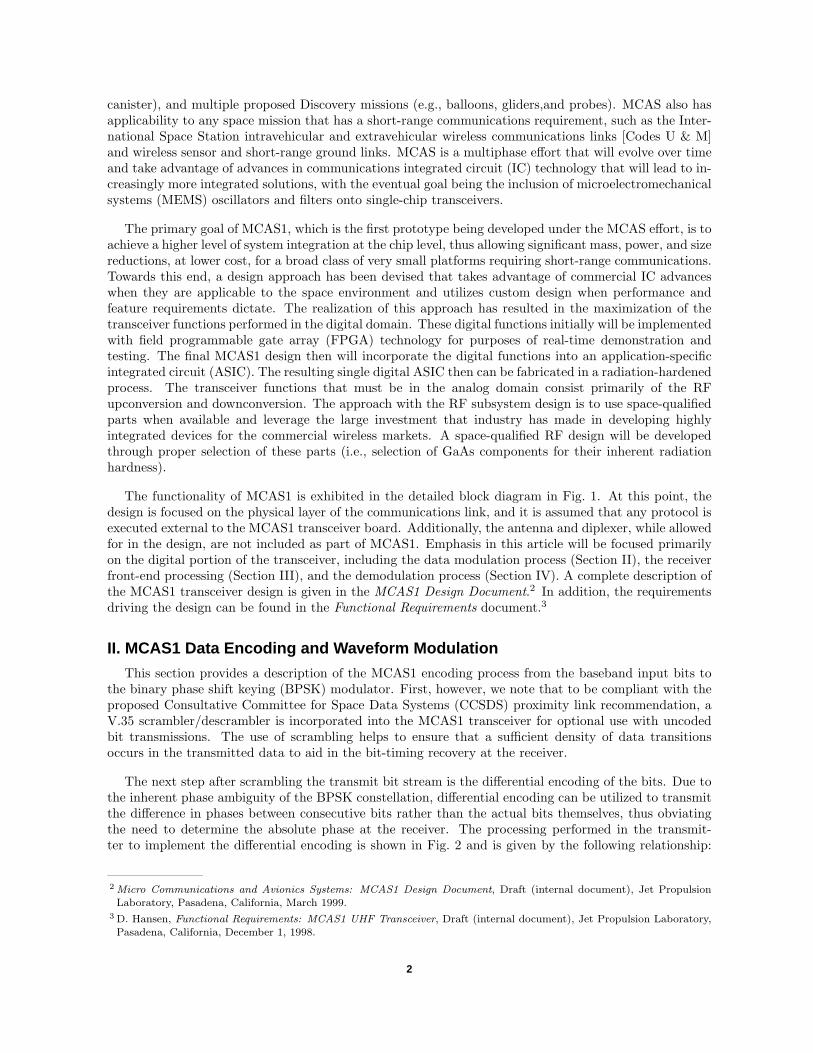
The functionality of MCAS1 is exhibited in the detailed block diagram in Fig. 1. At this point, thedesign is focused on the physical layer of the communications link, and it is assumed that any protocol isexecuted external to the MCAS1 transceiver board. Additionally, the antenna and diplexer, while allowedfor in the design, are not included as part of MCAS1. Emphasis in this article will be focused primarilyon the digital portion of the transceiver, including the data modulation process (Section II), the receiverfront-end processing (Section III), and the demodulation process (Section IV). A complete description ofthe MCAS1 transceiver design is given in the MCAS1 Design Document.2 In addition, the requirementsdriving the design can be found in the Functional Requirements document.3
II. MCAS1 Data Encoding and Waveform Modulation
This section provides a description of the MCAS1 encoding process from the baseband input bits tothe binary phase shift keying (BPSK) modulator. First, however, we note that to be compliant with theproposed Consultative Committee for Space Data Systems (CCSDS) proximity link recommendation, aV.35 scrambler/descrambler is incorporated into the MCAS1 transceiver for optional use with uncodedbit transmissions. The use of scrambling helps to ensure that a sufficient density of data transitionsoccurs in the transmitted data to aid in the bit-timing recovery at the receiver.
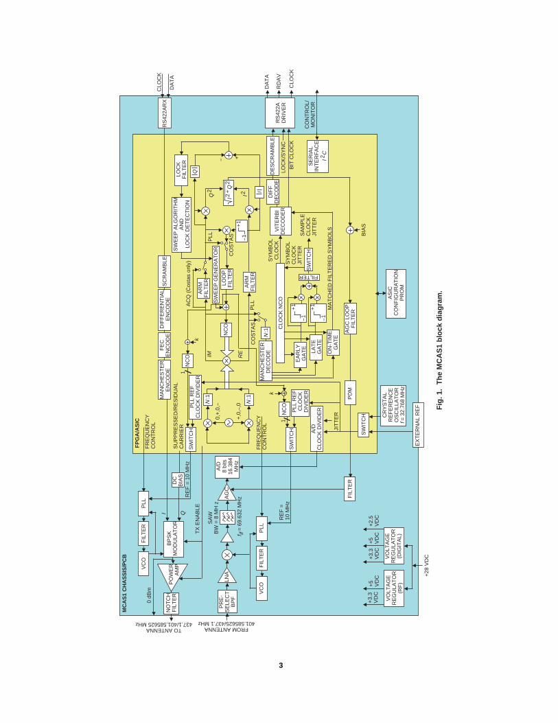
The next step after scrambling the transmit bit stream is the differential encoding of the bits. Due tothe inherent phase ambiguity of the BPSK constellation, differential encoding can be utilized to transmitthe difference in phases between consecutive bits rather than the actual bits themselves, thus obviatingthe need to determine the absolute phase at the receiver. The processing performed in the transmit-ter to implement the differential encoding is shown in Fig. 2 and is given by the following relationship:
2 Micro Communications and Avionics Systems: MCAS1 Design Document, Draft (internal document), Jet PropulsionLaboratory, Pasadena, California, March 1999.
3 D. Hansen, Functional Requirements: MCAS1 UHF Transceiver, Draft (internal document), Jet Propulsion Laboratory,Pasadena, California, December 1, 1998.
2
-1
AR
MF
ILT
ER
Q
MC
AS
1 C
HA
SS
IS/P
CB
0 dB
m
PO
WE
RA
MP
I QR
EF
= 1
0 M
Hz
TX
EN
AB
LE
LNA
RE
F =
10 M
Hz
+28
VD
C
+3.
3V
DC
+5
VD
C+
3.3
VD
C+
5V
DC
+2.
5V
DC
BIA
S
MA
TC
HE
D F
ILT
ER
ED
SY
MB
OLS
FROM ANTENNA401.585625/437.1 MHz
TO ANTENNA437.1/401.585625 MHz
FR
EQ
UE
NC
YC
ON
TR
OL
AG
C
SA
WB
W =
8 M
H z
f if =
69.
632
MH
z
FP
GA
/AS
IC
FR
EQ
UE
NC
YC
ON
TR
OL
SU
PP
RE
SS
ED
/RE
SID
UA
LC
AR
RIE
R1
0,+
,0,-
+,0
,-,0
1
k
k
JIT
TE
R
IM RE
CO
ST
AS
PLLA
CQ
(C
osta
s on
ly)
Q 2
PLL
CO
ST
AS
LOC
K/S
YN
C
BIT
CLO
CK
SY
MB
OL
CLO
CK
CO
NT
RO
L/M
ON
ITO
R
DA
TA
RD
AV
CLO
CK
SA
MP
LEC
LOC
KJI
TT
ER
SY
MB
OL
CLO
CK
JIT
TE
R
- +
I 2
CLO
CK
DA
TA
N :1
VC
OP
LLF
ILT
ER
NO
TC
HF
ILT
ER
BP
SK
MO
DU
LAT
OR
DC
BIA
S
PR
E-
SE
LEC
TB
PF
A/D
8 bi
ts16
.384
MH
z
VC
OP
LLF
ILT
ER
EX
TE
RN
AL
RE
F
VO
LTA
GE
RE
GU
LAT
OR
(RF
)
VO
LTA
GE
RE
GU
LAT
OR
(DIG
ITA
L)
CR
YS
TA
LR
EF
ER
EN
CE
OS
CIL
LAT
OR
f = 3
2.76
8 M
Hz
FIL
TE
R
PLL
RE
FC
LOC
KD
IVID
ER
PD
M
SW
ITC
H SW
ITC
HNC
O
A/D
CLO
CK
DIV
IDE
R
N :1
N :1M
AN
CH
ES
TE
RE
NC
OD
EF
EC
EN
CO
DE
DIF
FE
RE
NT
IAL
EN
CO
DE
NC
OP
LL R
EF
CLO
CK
DIV
IDE
RS
WIT
CH
MA
NC
HE
ST
ER
DE
CO
DE
AR
MF
ILT
ER
LOO
PF
ILT
ER
SW
EE
P A
LGO
RIT
HM
AN
DLO
CK
DE
TE
CT
ION
SW
ITC
H
EA
RLY
GA
TE
LAT
EG
AT
E
FILTER
AG
C L
OO
PF
ILT
ER
ON
-TIM
EG
AT
E
+1
-1
+1
CLO
CK
NC
O
NC
O
SW
EE
P G
EN
ER
AT
OR
SC
RA
MB
LE
LOC
KF
ILT
ER
-1+
1
RS
422A
DR
IVE
R
RS
422A
RX
DIF
FD
EC
OD
ED
ES
CR
AM
BLE
SE
RIA
LIN
TE
RF
AC
EI 2
C
VIT
ER
BI
DE
CO
DE
R
AS
ICC
ON
FIG
UR
AT
ION
PR
OM
Fig
. 1.
Th
e M
CA
S1
blo
ck d
iag
ram
.
I
I 2Q
2+
3
INPUT DATA OUTPUT DATA
Ts DELAY
Fig. 2. The differential encoder block diagram.
y(k) = x(k) + y(k − 1)
where x(k) = the input, y(k) = the output, and both are logical 0 or 1.
The differential encoder/decoder implementation of MCAS1 was procured as part of the Viterbi de-coder soft core acquired from Mentor Graphics [1]. Differential encoding may be enabled or disabled.
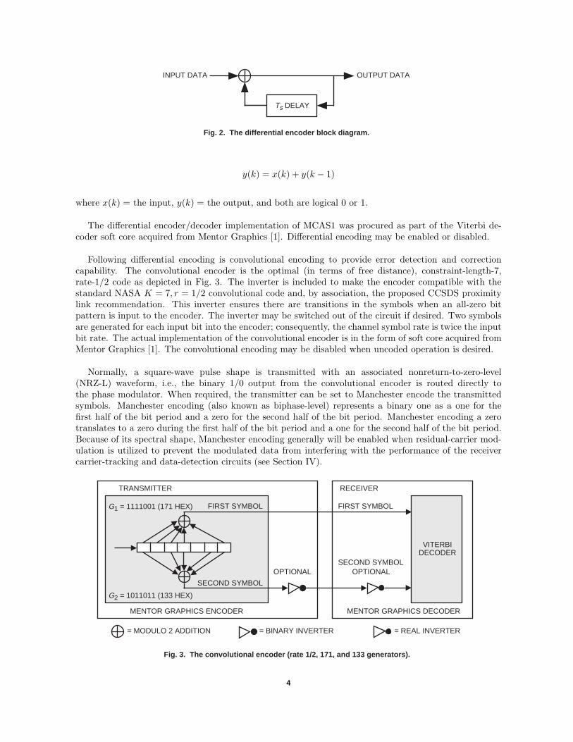
Following differential encoding is convolutional encoding to provide error detection and correctioncapability. The convolutional encoder is the optimal (in terms of free distance), constraint-length-7,rate-1/2 code as depicted in Fig. 3. The inverter is included to make the encoder compatible with thestandard NASA K = 7, r = 1/2 convolutional code and, by association, the proposed CCSDS proximitylink recommendation. This inverter ensures there are transitions in the symbols when an all-zero bitpattern is input to the encoder. The inverter may be switched out of the circuit if desired. Two symbolsare generated for each input bit into the encoder; consequently, the channel symbol rate is twice the inputbit rate. The actual implementation of the convolutional encoder is in the form of soft core acquired fromMentor Graphics [1]. The convolutional encoding may be disabled when uncoded operation is desired.
Normally, a square-wave pulse shape is transmitted with an associated nonreturn-to-zero-level(NRZ-L) waveform, i.e., the binary 1/0 output from the convolutional encoder is routed directly tothe phase modulator. When required, the transmitter can be set to Manchester encode the transmittedsymbols. Manchester encoding (also known as biphase-level) represents a binary one as a one for thefirst half of the bit period and a zero for the second half of the bit period. Manchester encoding a zerotranslates to a zero during the first half of the bit period and a one for the second half of the bit period.Because of its spectral shape, Manchester encoding generally will be enabled when residual-carrier mod-ulation is utilized to prevent the modulated data from interfering with the performance of the receivercarrier-tracking and data-detection circuits (see Section IV).
= MODULO 2 ADDITION
TRANSMITTER RECEIVER
FIRST SYMBOLFIRST SYMBOLG1 = 1111001 (171 HEX)
G2 = 1011011 (133 HEX)
SECOND SYMBOL
OPTIONALSECOND SYMBOL
OPTIONAL
VITERBIDECODER
MENTOR GRAPHICS DECODERMENTOR GRAPHICS ENCODER
= BINARY INVERTER = REAL INVERTER
Fig. 3. The convolutional encoder (rate 1/2, 171, and 133 generators).
4
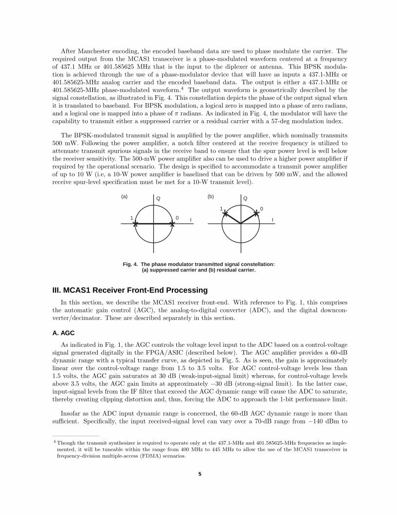
After Manchester encoding, the encoded baseband data are used to phase modulate the carrier. Therequired output from the MCAS1 transceiver is a phase-modulated waveform centered at a frequencyof 437.1 MHz or 401.585625 MHz that is the input to the diplexer or antenna. This BPSK modula-tion is achieved through the use of a phase-modulator device that will have as inputs a 437.1-MHz or401.585625-MHz analog carrier and the encoded baseband data. The output is either a 437.1-MHz or401.585625-MHz phase-modulated waveform.4 The output waveform is geometrically described by thesignal constellation, as illustrated in Fig. 4. This constellation depicts the phase of the output signal whenit is translated to baseband. For BPSK modulation, a logical zero is mapped into a phase of zero radians,and a logical one is mapped into a phase of π radians. As indicated in Fig. 4, the modulator will have thecapability to transmit either a suppressed carrier or a residual carrier with a 57-deg modulation index.
The BPSK-modulated transmit signal is amplified by the power amplifier, which nominally transmits500 mW. Following the power amplifier, a notch filter centered at the receive frequency is utilized toattenuate transmit spurious signals in the receive band to ensure that the spur power level is well belowthe receiver sensitivity. The 500-mW power amplifier also can be used to drive a higher power amplifier ifrequired by the operational scenario. The design is specified to accommodate a transmit power amplifierof up to 10 W (i.e, a 10-W power amplifier is baselined that can be driven by 500 mW, and the allowedreceive spur-level specification must be met for a 10-W transmit level).
Q
I
01
(b)
0
Q
I
(a)
1
Fig. 4. The phase modulator transmitted signal constellation:(a) suppressed carrier and (b) residual carrier.
III. MCAS1 Receiver Front-End Processing
In this section, we describe the MCAS1 receiver front-end. With reference to Fig. 1, this comprisesthe automatic gain control (AGC), the analog-to-digital converter (ADC), and the digital downcon-verter/decimator. These are described separately in this section.
A. AGC
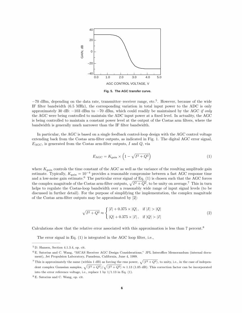
As indicated in Fig. 1, the AGC controls the voltage level input to the ADC based on a control-voltagesignal generated digitally in the FPGA/ASIC (described below). The AGC amplifier provides a 60-dBdynamic range with a typical transfer curve, as depicted in Fig. 5. As is seen, the gain is approximatelylinear over the control-voltage range from 1.5 to 3.5 volts. For AGC control-voltage levels less than1.5 volts, the AGC gain saturates at 30 dB (weak-input-signal limit) whereas, for control-voltage levelsabove 3.5 volts, the AGC gain limits at approximately −30 dB (strong-signal limit). In the latter case,input-signal levels from the IF filter that exceed the AGC dynamic range will cause the ADC to saturate,thereby creating clipping distortion and, thus, forcing the ADC to approach the 1-bit performance limit.
Insofar as the ADC input dynamic range is concerned, the 60-dB AGC dynamic range is more thansufficient. Specifically, the input received-signal level can vary over a 70-dB range from −140 dBm to
4 Though the transmit synthesizer is required to operate only at the 437.1-MHz and 401.585625-MHz frequencies as imple-mented, it will be tuneable within the range from 400 MHz to 445 MHz to allow the use of the MCAS1 transceiver infrequency-division multiple-access (FDMA) scenarios.
5
0.0 1.0 2.0 3.0 4.0 5.0
40
20
0
-20
-40
AGC CONTROL VOLTAGE, VG
AIN
, dB
Fig. 5. The AGC transfer curve.
−70 dBm, depending on the data rate, transmitter–receiver range, etc.5. However, because of the wideIF filter bandwidth (6.5 MHz), the corresponding variation in total input power to the ADC is onlyapproximately 30 dB: −103 dBm to −70 dBm, which could readily be maintained by the AGC if onlythe AGC were being controlled to maintain the ADC input power at a fixed level. In actuality, the AGCis being controlled to maintain a constant power level at the output of the Costas arm filters, where thebandwidth is generally much narrower than the IF filter bandwidth.
In particular, the AGC is based on a single feedback control-loop design with the AGC control voltageextending back from the Costas arm-filter outputs, as indicated in Fig. 1. The digital AGC error signal,EAGC, is generated from the Costas arm-filter outputs, I and Q, via
EAGC = Kgain ×(
1−√I2 +Q2
)(1)
where Kgain controls the time constant of the AGC as well as the variance of the resulting amplitude gainestimate. Typically, Kgain = 10−4 provides a reasonable compromise between a fast AGC response timeand a low-noise gain estimate.6 The particular error signal of Eq. (1) is chosen such that the AGC forcesthe complex magnitude of the Costas arm-filter outputs,
√I2 +Q2, to be unity on average.7 This in turn
helps to regulate the Costas-loop bandwidth over a reasonably wide range of input signal levels (to bediscussed in further detail). For the purpose of simplifying the implementation, the complex magnitudeof the Costas arm-filter outputs may be approximated by [2]:
√I2 +Q2 ≈
{ |I|+ 0.375× |Q| , if |I| > |Q|
|Q|+ 0.375× |I| , if |Q| > |I|(2)
Calculations show that the relative error associated with this approximation is less than 7 percent.8
The error signal in Eq. (1) is integrated in the AGC loop filter, i.e.,
5 D. Hansen, Section 4.1.3.4, op. cit.6 E. Satorius and C. Wang, “MCAS Receiver AGC Design Considerations,” JPL Interoffice Memorandum (internal docu-
ment), Jet Propulsion Laboratory, Pasadena, California, June 4, 1999.
7 This is approximately the same (within 1 dB) as forcing the rms power,√〈I2 +Q2〉, to unity, i.e., in the case of indepen-
dent complex Gaussian samples,√〈I2 +Q2〉/
√〈I2 +Q2〉 ≈ 1.13 (1.05 dB). This correction factor can be incorporated
into the error reference voltage, i.e., replace 1 by 1/1.13 in Eq. (1).8 E. Satorius and C. Wang, op. cit.
6
Vout = Vout + EAGC (3)
and the magnitude of the result, |Vout|, is used to generate the AGC gain, KAGC, via the nonlineartransfer curve, f(·), illustrated in Fig. 5, i.e.,
KAGC (dB) = f (|Vout|) (4)
This gain is then used to scale the AGC input.
A critical issue with this approach is the impact of the AGC on the operation of the ADC as well asthe internal digital arithmetic implemented in the FPGA/ASIC. As will be discussed in Section III.B,ideally the input ADC voltage is scaled to achieve an optimal trade-off between ADC quantization noiseand clipping distortion. In contrast, the AGC loop attempts to maintain the complex magnitude of theCostas arm-filter outputs to be unity on average. Thus, there is no guarantee that this criterion of unityrms Costas arm-filter outputs will enable the ADC to operate at its optimal input scaling (loading) pointor even prevent the ADC from saturating.
To alleviate this situation, fixed gains are distributed throughout the digital data paths.9 These gainsare programmable, dependent upon the data rate and the digital decimation factor (see Section III.C),and are used for purposes of minimizing the effects of digital quantization noise and saturation. Denotingthe product of these fixed gains by KF , we find that in steady state,10
KAGC ≈1
KF
√αsP + αnN0BIF
(5)
where P denotes the input signal power to the ADC; αs represents the fraction of this power reachingthe output of the Costas arm filters; N0 is the noise spectral level at the IF filter; and αn represents thefraction of the input noise power, N0BIF, that reaches the Costas arm-filter outputs.
By appropriate choice of KF , it has been shown that the AGC gain can be expressed as11
KAGC = K∗ADC × K̂AGC (6)
where K∗ADC denotes the optimal ADC loading point in the small signal limit and K̂AGC is the normalizedAGC gain, which is always less than unity. In this way, the AGC gain always scales the ADC input to itsoptimal loading point in the small signal limit and, as the signal power increases, the AGC gain decreasesfrom K∗ADC by the factor K̂AGC, thereby avoiding saturation at least until the AGC dynamic range isexceeded (see Fig. 1).
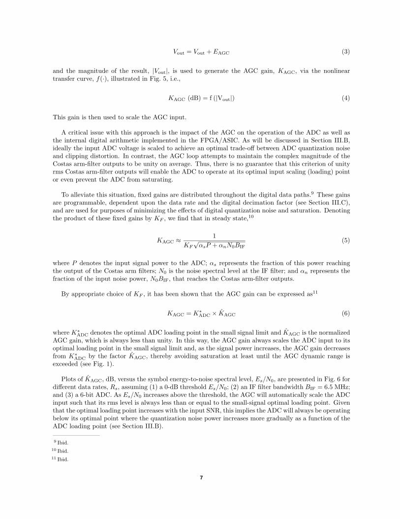
Plots of K̂AGC, dB, versus the symbol energy-to-noise spectral level, Es/N0, are presented in Fig. 6 fordifferent data rates, Rs, assuming (1) a 0-dB threshold Es/N0; (2) an IF filter bandwidth BIF = 6.5 MHz;and (3) a 6-bit ADC. As Es/N0 increases above the threshold, the AGC will automatically scale the ADCinput such that its rms level is always less than or equal to the small-signal optimal loading point. Giventhat the optimal loading point increases with the input SNR, this implies the ADC will always be operatingbelow its optimal point where the quantization noise power increases more gradually as a function of theADC loading point (see Section III.B).
9 Ibid.10 Ibid.11 Ibid.
7
-10
-15
0
-5
-20
-25
-30
-350 10 20 30 40 50 60
Rs = 2.048 Mb/s
Rs = 256 kb/s
Rs = 32 kb/s
Rs = 4 kb/s
Rs = 1 kb/s
Es /N 0, dB20
log 1
0 K
AG
C
Fig. 6. KAGC , dB, versus Es /N 0 fordifferent data rates.
As the input-signal power level increases, K̂AGC continues to decrease until the signal power becomescommensurate with the total input noise power, N0BIF. Beyond this, K̂AGC asymptotes to a leveldependent upon the data rate—the higher the data rate, the larger the asymptotic level of K̂AGC. Thelower data rates impose the most severe constraint on the usable AGC dynamic range. For example,when Rs = 1 kb/s, K̂AGC asymptotes to approximately −33 dB or, equivalently, the AGC gain KAGC
decreases to 33-dB below the optimal small-signal loading point of the ADC. Referring to Section III.B(Fig. 10), this approximately matches the dynamic range of a 6-bit ADC, i.e., at 30-dB below the optimalsmall-signal loading point of a 6-bit ADC, the quantization noise power equals the total input power.
To be conservative, we define the worst-case AGC dynamic range corresponding to the lowest symbolrates, 1–4 kb/s, to be the point at which KAGC falls to 25-dB below the optimal small-signal loadingpoint for a 6-bit ADC. With reference ahead to Fig. 10, this corresponds to an input-to-quantization noisepower ratio of 5 dB for a 6-bit ADC and, with reference to Fig. 6, this also corresponds to a signal-powerdynamic range, Es/N0, of approximately 30 dB at either Rs = 1 or 4 kb/s. This (30 dB) is sufficientto cover the signal dynamic range due to transmitter–receiver range or antenna-pattern variations. Notefrom Fig. 6 that, at the larger data rates, e.g., 32 kb/s and above, the AGC gain remains well within theADC dynamic range for all values of Es/N0, and, thus, the maximum allowable signal dynamic range inthese cases matches the entire AGC dynamic range of 60 dB. Large signals exceeding this dynamic rangeultimately will cause clipping distortion at the ADC.
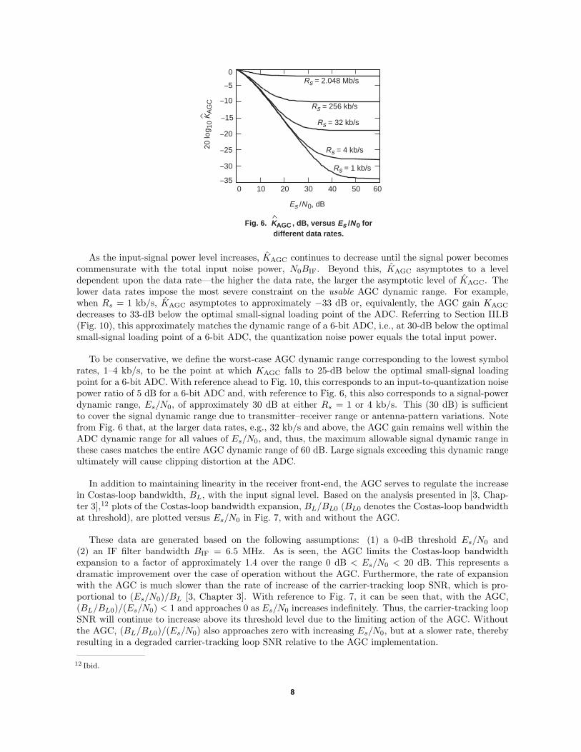
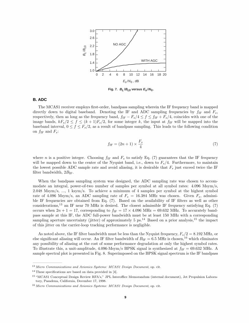
In addition to maintaining linearity in the receiver front-end, the AGC serves to regulate the increasein Costas-loop bandwidth, BL, with the input signal level. Based on the analysis presented in [3, Chap-ter 3],12 plots of the Costas-loop bandwidth expansion, BL/BL0 (BL0 denotes the Costas-loop bandwidthat threshold), are plotted versus Es/N0 in Fig. 7, with and without the AGC.
These data are generated based on the following assumptions: (1) a 0-dB threshold Es/N0 and(2) an IF filter bandwidth BIF = 6.5 MHz. As is seen, the AGC limits the Costas-loop bandwidthexpansion to a factor of approximately 1.4 over the range 0 dB < Es/N0 < 20 dB. This represents adramatic improvement over the case of operation without the AGC. Furthermore, the rate of expansionwith the AGC is much slower than the rate of increase of the carrier-tracking loop SNR, which is pro-portional to (Es/N0)/BL [3, Chapter 3]. With reference to Fig. 7, it can be seen that, with the AGC,(BL/BL0)/(Es/N0) < 1 and approaches 0 as Es/N0 increases indefinitely. Thus, the carrier-tracking loopSNR will continue to increase above its threshold level due to the limiting action of the AGC. Withoutthe AGC, (BL/BL0)/(Es/N0) also approaches zero with increasing Es/N0, but at a slower rate, therebyresulting in a degraded carrier-tracking loop SNR relative to the AGC implementation.
12 Ibid.
8
0 2 4 6 8 10 12 14 16 18 201.0
1.4
1.8
2.6
3.0
2.2 NO AGC
WITH AGC
BL
/BL0
Es /N 0 , dB
Fig. 7. BL /BL0 versus Es /N 0 .
B. ADC
The MCAS1 receiver employs first-order, bandpass sampling wherein the IF frequency band is mappeddirectly down to digital baseband. Denoting the IF and ADC sampling frequencies by fIF and Fs,respectively, then as long as the frequency band, fIF − Fs/4 ≤ f ≤ fIF + Fs/4, coincides with one of theimage bands, kFs/2 ≤ f ≤ (k + 1)Fs/2, for some integer k, the input at fIF will be mapped into thebaseband interval, 0 ≤ f ≤ Fs/2, as a result of bandpass sampling. This leads to the following conditionon fIF and Fs:
fIF = (2n+ 1)× Fs4
(7)
where n is a positive integer. Choosing fIF and Fs to satisfy Eq. (7) guarantees that the IF frequencywill be mapped down to the center of the Nyquist band, i.e., down to Fs/4. Furthermore, to maintainthe lowest possible ADC sample rate and avoid aliasing, it is desirable that Fs just exceed twice the IFfilter bandwidth, 2BIF.
When the bandpass sampling system was designed, the ADC sampling rate was chosen to accom-modate an integral, power-of-two number of samples per symbol at all symbol rates: 4.096 Msym/s,2.048 Msym/s, ..., 1 ksym/s. To achieve a minimum of 4 samples per symbol at the highest symbolrate of 4.096 Msym/s, an ADC sampling rate of Fs = 16.384 MHz was chosen. Given Fs, admissi-ble IF frequencies are obtained from Eq. (7). Based on the availability of IF filters as well as otherconsiderations,13 an IF near 70 MHz is desired. The closest admissible IF frequency satisfying Eq. (7)occurs when 2n + 1 = 17, corresponding to fIF = 17 × 4.096 MHz = 69.632 MHz. To accurately band-pass sample at this IF, the ADC full-power bandwidth must be at least 150 MHz with a correspondingsampling aperture uncertainty (jitter) of approximately 5 ps.14 Based on a prior analysis,15 the impactof this jitter on the carrier-loop tracking performance is negligible.
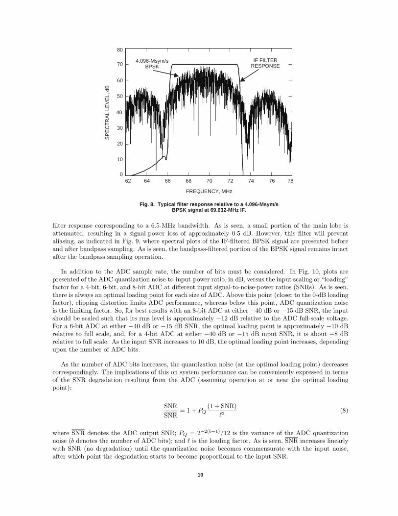
As noted above, the IF filter bandwidth must be less than the Nyquist frequency, Fs/2 = 8.192 MHz, orelse significant aliasing will occur. An IF filter bandwidth of BIF = 6.5 MHz is chosen,16 which eliminatesany possibility of aliasing at the cost of some performance degradation at only the highest symbol rates.To illustrate this, a unit-amplitude, 4.096-Msym/s BPSK signal is synthesized at fIF = 69.632 MHz. Asample spectral plot is presented in Fig. 8. Superimposed on the BPSK signal spectrum is the IF bandpass
13 Micro Communications and Avionics Systems: MCAS1 Design Document, op. cit.14 These specifications are based on data provided in [4].15 “MCAS1 Conceptual Design Review RFA’s,” JPL Interoffice Memorandum (internal document), Jet Propulsion Labora-
tory, Pasadena, California, December 17, 1998.16 Micro Communications and Avionics Systems: MCAS1 Design Document, op. cit.
9
62 64 66 68 70 72 74 76 780
10
20
30
40
50
60
70
80
IF FILTERRESPONSE
4.096-Msym/sBPSK
SP
EC
TR
AL
LEV
EL,
dB
FREQUENCY, MHz
Fig. 8. Typical filter response relative to a 4.096-Msym/sBPSK signal at 69.632-MHz IF.
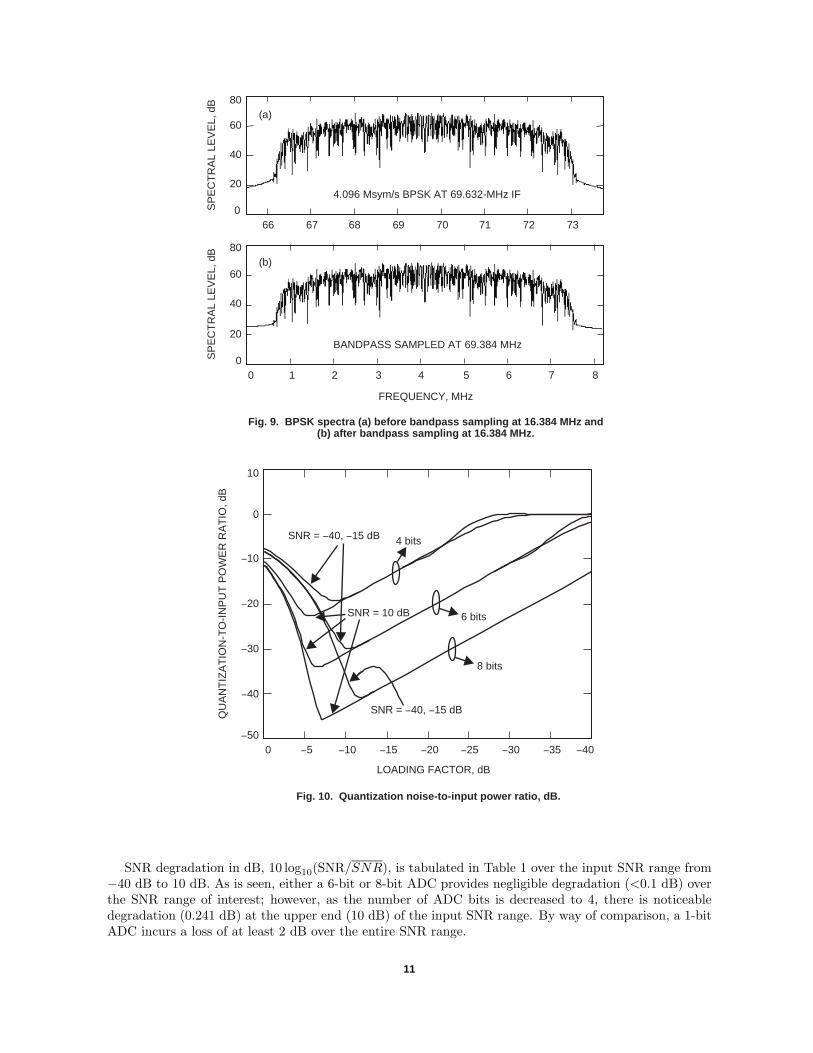
filter response corresponding to a 6.5-MHz bandwidth. As is seen, a small portion of the main lobe isattenuated, resulting in a signal-power loss of approximately 0.5 dB. However, this filter will preventaliasing, as indicated in Fig. 9, where spectral plots of the IF-filtered BPSK signal are presented beforeand after bandpass sampling. As is seen, the bandpass-filtered portion of the BPSK signal remains intactafter the bandpass sampling operation.
In addition to the ADC sample rate, the number of bits must be considered. In Fig. 10, plots arepresented of the ADC quantization noise-to-input-power ratio, in dB, versus the input scaling or “loading”factor for a 4-bit, 6-bit, and 8-bit ADC at different input signal-to-noise-power ratios (SNRs). As is seen,there is always an optimal loading point for each size of ADC. Above this point (closer to the 0-dB loadingfactor), clipping distortion limits ADC performance, whereas below this point, ADC quantization noiseis the limiting factor. So, for best results with an 8-bit ADC at either −40 dB or −15 dB SNR, the inputshould be scaled such that its rms level is approximately −12 dB relative to the ADC full-scale voltage.For a 6-bit ADC at either −40 dB or −15 dB SNR, the optimal loading point is approximately −10 dBrelative to full scale, and, for a 4-bit ADC at either −40 dB or −15 dB input SNR, it is about −8 dBrelative to full scale. As the input SNR increases to 10 dB, the optimal loading point increases, dependingupon the number of ADC bits.
As the number of ADC bits increases, the quantization noise (at the optimal loading point) decreasescorrespondingly. The implications of this on system performance can be conveniently expressed in termsof the SNR degradation resulting from the ADC (assuming operation at or near the optimal loadingpoint):
SNRSNR
= 1 + PQ(1 + SNR)
`2(8)
where SNR denotes the ADC output SNR; PQ = 2−2(b−1)/12 is the variance of the ADC quantizationnoise (b denotes the number of ADC bits); and ` is the loading factor. As is seen, SNR increases linearlywith SNR (no degradation) until the quantization noise becomes commensurate with the input noise,after which point the degradation starts to become proportional to the input SNR.
10
4.096 Msym/s BPSK AT 69.632-MHz IF
66 67 68 69 70 71 72 730
20
40
60
80
0 1 2 3 4 5 6 70
20
40
60
80
8
FREQUENCY, MHz
Fig. 9. BPSK spectra (a) before bandpass sampling at 16.384 MHz and(b) after bandpass sampling at 16.384 MHz.
(a)
(b)
BANDPASS SAMPLED AT 69.384 MHz
SP
EC
TR
AL
LEV
EL,
dB
SP
EC
TR
AL
LEV
EL,
dB
4 bits
6 bits
8 bits
SNR = -40, -15 dB
SNR = 10 dB
SNR = -40, -15 dB
0 -5 -10 -15 -20 -25 -30 -35 -40
10
0
-10
-20
-30
-40
-50
LOADING FACTOR, dB
QU
AN
TIZ
AT
ION
-TO
-IN
PU
T P
OW
ER
RA
TIO
, dB
Fig. 10. Quantization noise-to-input power ratio, dB.
SNR degradation in dB, 10 log10(SNR/SNR), is tabulated in Table 1 over the input SNR range from−40 dB to 10 dB. As is seen, either a 6-bit or 8-bit ADC provides negligible degradation (<0.1 dB) overthe SNR range of interest; however, as the number of ADC bits is decreased to 4, there is noticeabledegradation (0.241 dB) at the upper end (10 dB) of the input SNR range. By way of comparison, a 1-bitADC incurs a loss of at least 2 dB over the entire SNR range.
11
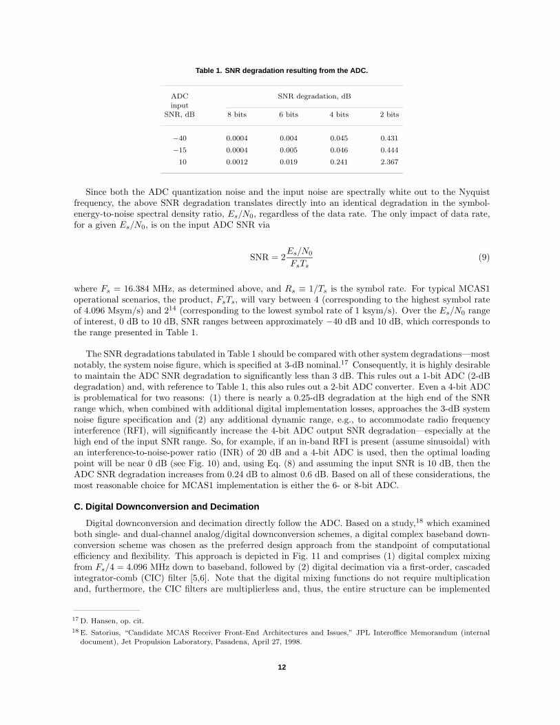
Table 1. SNR degradation resulting from the ADC.
ADC SNR degradation, dBinput
SNR, dB 8 bits 6 bits 4 bits 2 bits
−40 0.0004 0.004 0.045 0.431
−15 0.0004 0.005 0.046 0.444
10 0.0012 0.019 0.241 2.367
Since both the ADC quantization noise and the input noise are spectrally white out to the Nyquistfrequency, the above SNR degradation translates directly into an identical degradation in the symbol-energy-to-noise spectral density ratio, Es/N0, regardless of the data rate. The only impact of data rate,for a given Es/N0, is on the input ADC SNR via
SNR = 2Es/N0
FsTs(9)
where Fs = 16.384 MHz, as determined above, and Rs ≡ 1/Ts is the symbol rate. For typical MCAS1operational scenarios, the product, FsTs, will vary between 4 (corresponding to the highest symbol rateof 4.096 Msym/s) and 214 (corresponding to the lowest symbol rate of 1 ksym/s). Over the Es/N0 rangeof interest, 0 dB to 10 dB, SNR ranges between approximately −40 dB and 10 dB, which corresponds tothe range presented in Table 1.
The SNR degradations tabulated in Table 1 should be compared with other system degradations—mostnotably, the system noise figure, which is specified at 3-dB nominal.17 Consequently, it is highly desirableto maintain the ADC SNR degradation to significantly less than 3 dB. This rules out a 1-bit ADC (2-dBdegradation) and, with reference to Table 1, this also rules out a 2-bit ADC converter. Even a 4-bit ADCis problematical for two reasons: (1) there is nearly a 0.25-dB degradation at the high end of the SNRrange which, when combined with additional digital implementation losses, approaches the 3-dB systemnoise figure specification and (2) any additional dynamic range, e.g., to accommodate radio frequencyinterference (RFI), will significantly increase the 4-bit ADC output SNR degradation—especially at thehigh end of the input SNR range. So, for example, if an in-band RFI is present (assume sinusoidal) withan interference-to-noise-power ratio (INR) of 20 dB and a 4-bit ADC is used, then the optimal loadingpoint will be near 0 dB (see Fig. 10) and, using Eq. (8) and assuming the input SNR is 10 dB, then theADC SNR degradation increases from 0.24 dB to almost 0.6 dB. Based on all of these considerations, themost reasonable choice for MCAS1 implementation is either the 6- or 8-bit ADC.
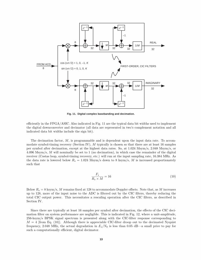
C. Digital Downconversion and Decimation
Digital downconversion and decimation directly follow the ADC. Based on a study,18 which examinedboth single- and dual-channel analog/digital downconversion schemes, a digital complex baseband down-conversion scheme was chosen as the preferred design approach from the standpoint of computationalefficiency and flexibility. This approach is depicted in Fig. 11 and comprises (1) digital complex mixingfrom Fs/4 = 4.096 MHz down to baseband, followed by (2) digital decimation via a first-order, cascadedintegrator-comb (CIC) filter [5,6]. Note that the digital mixing functions do not require multiplicationand, furthermore, the CIC filters are multiplierless and, thus, the entire structure can be implemented
17 D. Hansen, op. cit.
18 E. Satorius, “Candidate MCAS Receiver Front-End Architectures and Issues,” JPL Interoffice Memorandum (internaldocument), Jet Propulsion Laboratory, Pasadena, April 27, 1998.
12
Z -1
M8 REAL
321/M
-1
32 32 32
FIRST-ORDER, CIC FILTERScos (pn / 2) = 1, 0, -1, K
sin (pn / 2) = 0, 1, 0, K
M
8
IMAGINARY
321/M
-1
32 32 32
FROM ACD
Fig. 11. Digital complex basebanding and decimation.
8
Z -1
Z -1Z -1
efficiently in the FPGA/ASIC. Also indicated in Fig. 11 are the typical data bit widths used to implementthe digital downconverter and decimator (all data are represented in two’s complement notation and allindicated data bit widths include the sign bit).
The decimation factor, M , is programmable and is dependent upon the input data rate. To accom-modate symbol-timing recovery (Section IV), M typically is chosen so that there are at least 16 samplesper symbol after decimation, except at the highest data rates. So, at 1.024 Msym/s, 2.048 Msym/s, or4.096 Msym/s, M will nominally be set to 1 (no decimation), in which case the remainder of the digitalreceiver (Costas loop, symbol-timing recovery, etc.) will run at the input sampling rate, 16.384 MHz. Asthe data rate is lowered below Rs = 1.024 Msym/s down to 8 ksym/s, M is increased proportionatelysuch that
FsRs ×M
= 16 (10)
Below Rs = 8 ksym/s, M remains fixed at 128 to accommodate Doppler offsets. Note that, as M increasesup to 128, more of the input noise to the ADC is filtered out by the CIC filters, thereby reducing thetotal CIC output power. This necessitates a rescaling operation after the CIC filters, as described inSection IV.
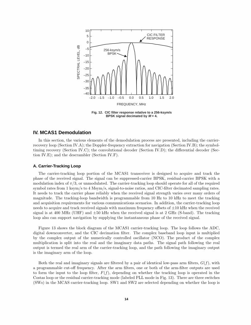
Since there are typically at least 16 samples per symbol after decimation, the effects of the CIC deci-mation filter on system performance are negligible. This is indicated in Fig. 12, where a unit-amplitude,256-ksym/s BPSK signal spectrum is presented along with the CIC-filter response corresponding toM = 4 [from Eq. (10)]. Although there is appreciable CIC-filter droop out to the decimated Nyquistfrequency, 2.048 MHz, the actual degradation in Es/N0 is less than 0.05 dB—a small price to pay forsuch a computationally efficient, digital decimator.
13
-2.0 -1.5 -1.0 -0.5 0.0 0.5 1.0 1.5 2.0-40
-35
-30
-25
-20
-15
-10
-5
0
5
10CIC FILTERRESPONSE
256-ksym/sBPSK
FREQUENCY, MHz
SP
EC
TR
AL
LEV
EL,
dB
Fig. 12. CIC filter response relative to a 256-ksym/sBPSK signal decimated by M = 4.
IV. MCAS1 Demodulation
In this section, the various elements of the demodulation process are presented, including the carrier-recovery loop (Section IV.A); the Doppler-frequency extraction for navigation (Section IV.B); the symbol-timing recovery (Section IV.C); the convolutional decoder (Section IV.D); the differential decoder (Sec-tion IV.E); and the descrambler (Section IV.F).
A. Carrier-Tracking Loop
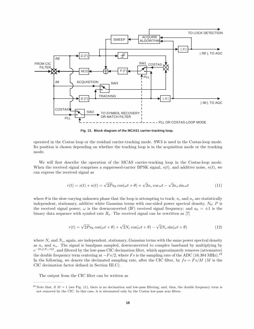
The carrier-tracking loop portion of the MCAS1 transceiver is designed to acquire and track thephase of the received signal. The signal can be suppressed-carrier BPSK, residual-carrier BPSK with amodulation index of π/3, or unmodulated. The carrier-tracking loop should operate for all of the requiredsymbol rates from 1 ksym/s to 4 Msym/s, signal-to-noise ratios, and CIC-filter decimated sampling rates.It needs to track the carrier phase reliably when the received signal strength varies over many orders ofmagnitude. The tracking-loop bandwidth is programmable from 10 Hz to 10 kHz to meet the trackingand acquisition requirements for various communications scenarios. In addition, the carrier-tracking loopneeds to acquire and track received signals with maximum frequency offsets of ±10 kHz when the receivedsignal is at 400 MHz (UHF) and ±50 kHz when the received signal is at 2 GHz (S-band). The trackingloop also can support navigation by supplying the instantaneous phase of the received signal.
Figure 13 shows the block diagram of the MCAS1 carrier-tracking loop. The loop follows the ADC,digital downconverter, and the CIC decimation filter. The complex baseband loop input is multipliedby the complex output of the numerically controlled oscillator (NCO). The product of the complexmultiplication is split into the real and the imaginary data paths. The signal path following the realoutput is termed the real arm of the carrier-tracking loop, and the path following the imaginary outputis the imaginary arm of the loop.
Both the real and imaginary signals are filtered by a pair of identical low-pass arm filters, G(f), witha programmable cut-off frequency. After the arm filters, one or both of the arm-filter outputs are usedto form the input to the loop filter, F (f), depending on whether the tracking loop is operated in theCostas loop or the residual carrier-tracking mode (labeled PLL mode in Fig. 13). There are three switches(SWs) in the MCAS carrier-tracking loop. SW1 and SW2 are selected depending on whether the loop is
14
SWEEP
PLL
SW2 TO SYMBOL RECOVERYOR MATCH FILTER
G (f )
G (f )
NCO F (f )
RE
IM
PLL OR COSTAS-LOOP MODE
SW3ACQUISITION
TRACKING
TO LOCK DETECTIONACQUIRE
ALGORITHM
SW1 COSTAS
PLL
| X |
| X || RE |, TO AGC
| IM |, TO AGC
FROM CICFILTER
COSTAS
Fig. 13. Block diagram of the MCAS1 carrier-tracking loop.
operated in the Costas loop or the residual carrier-tracking mode. SW3 is used in the Costas-loop mode.Its position is chosen depending on whether the tracking loop is in the acquisition mode or the trackingmode.
We will first describe the operation of the MCAS carrier-tracking loop in the Costas-loop mode.When the received signal comprises a suppressed-carrier BPSK signal, s(t), and additive noise, n(t), wecan express the received signal as
r(t) = s(t) + n(t) =√
2Pak cos(ωt+ θ) +√
2nc cosωt−√
2ns sinωt (11)
where θ is the slow-varying unknown phase that the loop is attempting to track; nc and ns are statisticallyindependent, stationary, additive white Gaussian terms with one-sided power spectral density, N0; P isthe received signal power; ω is the downconverted (IF) received signal frequency; and ak = ±1 is thebinary data sequence with symbol rate Rs. The received signal can be rewritten as [7]
r(t) =√
2Pak cos(ωt+ θ) +√
2Nc cos(ωt+ θ)−√
2Ns sin(ωt+ θ) (12)
whereNc andNs, again, are independent, stationary, Gaussian terms with the same power spectral densityas nc and ns. The signal is bandpass sampled, downconverted to complex baseband by multiplying bye−2πj(Fs/4)t, and filtered by the low-pass CIC decimation filter, which approximately removes (attenuates)the double frequency term centering at −Fs/2, where Fs is the sampling rate of the ADC (16.384 MHz).19
In the following, we denote the decimated sampling rate, after the CIC filter, by fs = Fs/M (M is theCIC decimation factor defined in Section III.C).
The output from the CIC filter can be written as
19 Note that, if M = 1 (see Fig. 11), there is no decimation and low-pass filtering, and, thus, the double frequency term isnot removed by the CIC. In this case, it is attenuated only by the Costas low-pass arm filters.
15
LPF(r(t)× e−jωt) =√
22
[√Pak cos θ +Nc cos θ −Ns sin θ
]+ j
√2
2
[√Pak sin θ +Nc sin θ +Ns cos θ
](13)
The signal then is multiplied by e−jθ̂, where θ̂ is the carrier-tracking loop estimate of θ. The product ofthe complex multiplication is
LPF(r(t)× e−jωt)× e−jθ̂ =√
22
[√Pak cosϕ+Nc cosϕ−Ns sinϕ
]
+ j
√2
2
[√Pak sinϕ+Nc sinϕ+Ns cosϕ
](14)
where ϕ = θ − θ̂. We note that, since the tracking loop operates in baseband, there are no doublefrequency terms. When the loop is locked, i.e. ϕ ≈ 0, the received data, ak, can be recovered from thereal part of the product. The real and the imaginary parts of the product are identical to the outputsof the in-phase and quadrature-phase detectors of a conventional passband Costas loop except for theconstant coefficient
√2/2, which arises from the approximate removal of the double frequency term by
the CIC filter and/or the Costas low-pass arm filters. With proper scaling, the complex implementationof the MCAS1 carrier-tracking loop has performance identical to a conventional passband Costas loopwith its NCO operating at the carrier frequency, ω [8].
When the received signal is a suppressed-carrier BPSK signal, the real and the imaginary outputsof the complex multiplication are filtered by a pair of programmable arm filters, G(f). The arm filtersare discrete implementations of a first-order low-pass Butterworth filter with a programmable cut-offfrequency. The arm filters are used to reduce noise in the carrier-tracking loop, but the cut-off frequencyshould not be so low that the signal power is reduced by the arm filters significantly. It is found that thecut-off frequency that minimizes the tracking-loop error for the arm filters is approximately equal to thereceived symbol rate, Rs, for nonreturn-to-zero (NRZ)-coded data [3,9]. For the MCAS receiver, therecan be from 4 to 128 samples per symbol (after CIC decimation). Therefore, the cut-off frequency needsto be programmable between fs/128 and fs/4.
When the received signal is a suppressed-carrier BPSK signal, the output of the real arm filter ispassed through a hard limiter with the output equal to +1 or −1 depending on the polarity of the realarm-filter output. It has been shown that, with the operating Es/No at 0 dB or above, the limiter canreduce the squaring loss, SL, of the Costas loops [3]. Squaring loss is caused by the multiplication of thereal and imaginary arm signals. This operation is required to remove the data polarity. The penalty ofthis squaring operation is that noise in the imaginary arm is multiplied by both the signal and noise ofthe real arm, resulting in poorer noise performance. With the hard limiter, the cross-multiplier beforethe loop filter, F (f), can be replaced by a combination of a switch and an inverter. The input to the loopfilter is inverted when the output of the real arm-filter output is negative. Instead of a real multiplier, theswitch and inverter reduce the complexity of the digital circuits, thus reducing the power consumption.A Costas loop with a hard limiter is termed a polarity-type Costas loop.
The MCAS1 carrier-tracking loop is a second-order loop. A second-order loop has the advantage ofbeing able to track a constant frequency offset without incurring any tracking error and possesses goodstability properties. The transfer function of a second-order, continuous-time loop is
16
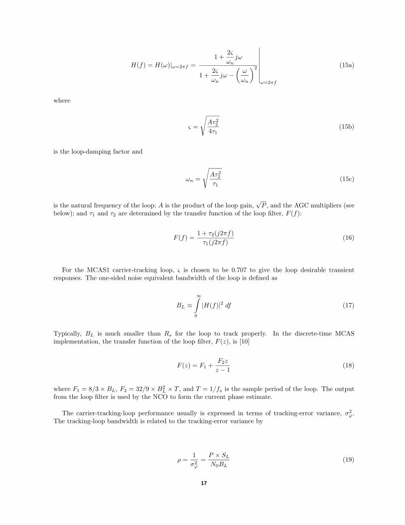
H(f) = H(ω)|ω=2πf =1 +
2ςωnjω
1 +2ςωnjω −
(ω
ωn
)2
∣∣∣∣∣∣∣∣∣ω=2πf
(15a)
where
ς =
√Aτ2
2
4τ1(15b)
is the loop-damping factor and
ωn =
√Aτ2
2
τ1(15c)
is the natural frequency of the loop; A is the product of the loop gain,√P , and the AGC multipliers (see
below); and τ1 and τ2 are determined by the transfer function of the loop filter, F (f):
F (f) =1 + τ2(j2πf)τ1(j2πf)
(16)
For the MCAS1 carrier-tracking loop, ς is chosen to be 0.707 to give the loop desirable transientresponses. The one-sided noise equivalent bandwidth of the loop is defined as
BL ≡∞∫
0
|H(f)|2 df (17)
Typically, BL is much smaller than Rs for the loop to track properly. In the discrete-time MCASimplementation, the transfer function of the loop filter, F (z), is [10]
F (z) = F1 +F2z
z − 1(18)
where F1 = 8/3×BL, F2 = 32/9×B2L × T , and T = 1/fs is the sample period of the loop. The output
from the loop filter is used by the NCO to form the current phase estimate.
The carrier-tracking-loop performance usually is expressed in terms of tracking-error variance, σ2ϕ.
The tracking-loop bandwidth is related to the tracking-error variance by
ρ =1σ2ϕ
=P × SLN0BL
(19)
17
where ρ is the tracking-loop signal-to-noise ratio, i.e., the loop SNR, and SL is the squaring loss and isbetween −3 dB and −0.3 dB, depending on Es/N0 and the arm-filter bandwidth [3]. It is found that, inorder for the Costas loop to track reliably with low probability of loss of lock and cycle slips, the loopSNR should be above the following threshold: ρ ≥ 17 dB.
In other words, the tracking-loop bandwidth, BL, should be chosen to be small enough to meet theabove inequality and yet large enough to reduce acquisition time. Equivalently,
BL ≤ 100.1×(10∗ log 10(P/N0)+SL[dB]−17) = 100.1×(Es/N0[dB]+10∗ log 10(Rs)+SL[dB]−17) (20)
where the last equality follows from P = Es × RS for suppressed-carrier BPSK signals. The above loopSNR threshold of 17 dB, however, is not a hard limit. If the loop SNR is only slightly less than 17 dB, thecarrier-tracking loop should still track the received phase reliably. However, as ρ continues to decrease,the loop will start to lose lock and experience more frequent cycle slips.
From Eqs. (15) and (17), the tracking-loop bandwidth, BL, and the loop-damping factor are functionsof the AGC gain. From Eq. (5),
KAGCT ×√αPP
2+ αNRsN0 = 1 (21)
where KAGCT denotes the product of the AGC multiplier, KAGC, and the fixed gains, KF , i.e., KAGCT ≡KAGC ×KF (see Section III.A); αP is the fraction of the signal power at the input to the Costas loopthat reaches the output of the arm filters; and αN represents the fraction of the noise power in the signalbandwidth, RsN0, that reaches the output of the arm filters. Both αP and αN are functions of thearm-filter cut-off frequency, which in turn depends on the throughput rate of the loop in terms of thenumber of samples per symbol. They are independent of the received signal power.
We now denote the output of the real arm filter as [GRE(f)]out. The contribution of the signal at theinput of the loop filter is equal to
KAGCT ×√αPP
2× sgn{[GRE(f)]out} × sinϕ (22)
where sgn{x} is the signum function and is equal to 1 when x > 0 and −1 when x < 0. The MCAScarrier-tracking loop is designed so that the magnitude of the input to the loop filter is equal to 1 at thethreshold value of Es/N0 (typically 0 dB). Thus, we multiply the input to the loop filter by the factor1/(KAGCT ×
√αPP/2), evaluated at threshold. This is termed the bandwidth correction factor. From
Eq. (21),
1KAGCT ×
√αPP/2
∣∣∣∣∣Es/N0=threshold
=√
1 + 2αN
αP × Es/N0
∣∣∣∣Es/N0=threshold
(23)
The bandwidth-correction factor is a function of the threshold Es/N0 as well as of the number ofsamples per symbol and is independent of the data rate. As discussed in Section III.A (see Fig. 7), asEs/N0 increases above threshold, the loop bandwidth will expand correspondingly—however, at such aslow rate that the tracking-loop SNR also will continue to increase as desired.
18
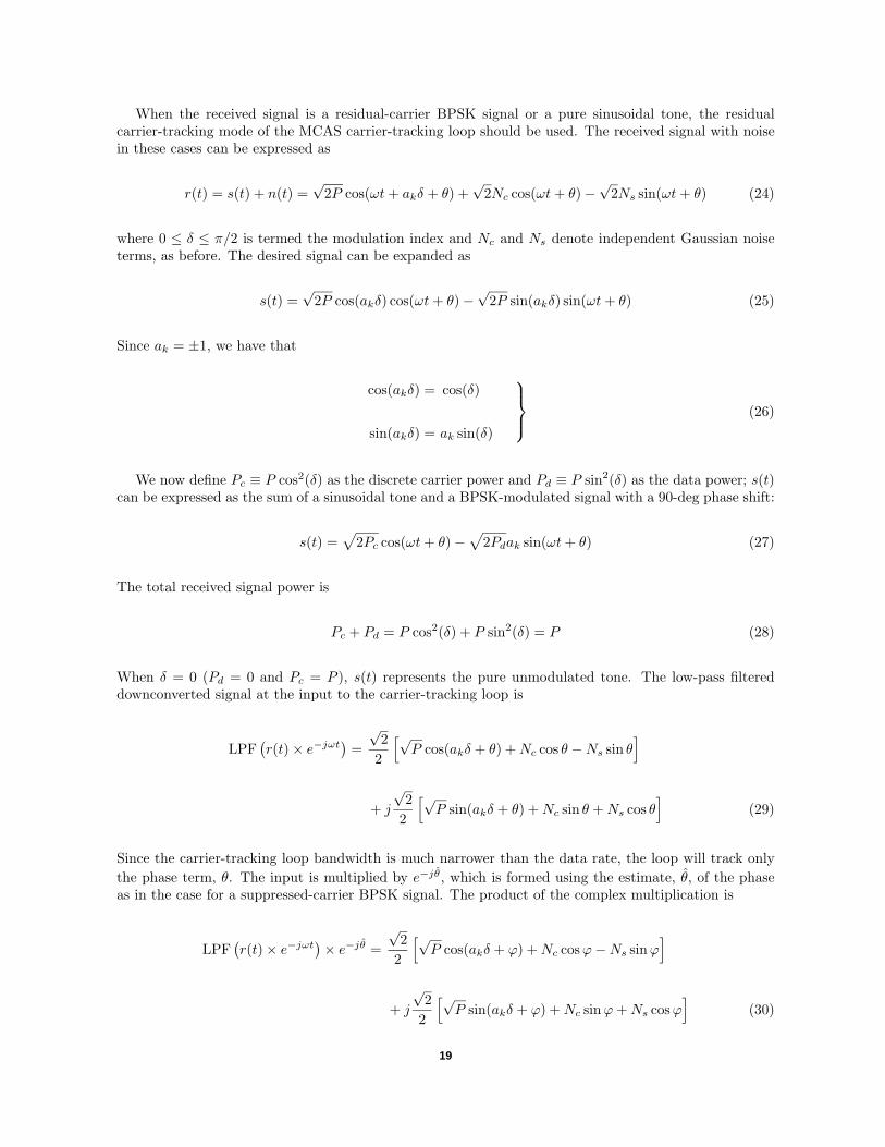
When the received signal is a residual-carrier BPSK signal or a pure sinusoidal tone, the residualcarrier-tracking mode of the MCAS carrier-tracking loop should be used. The received signal with noisein these cases can be expressed as
r(t) = s(t) + n(t) =√
2P cos(ωt+ akδ + θ) +√
2Nc cos(ωt+ θ)−√
2Ns sin(ωt+ θ) (24)
where 0 ≤ δ ≤ π/2 is termed the modulation index and Nc and Ns denote independent Gaussian noiseterms, as before. The desired signal can be expanded as
s(t) =√
2P cos(akδ) cos(ωt+ θ)−√
2P sin(akδ) sin(ωt+ θ) (25)
Since ak = ±1, we have that
cos(akδ) = cos(δ)
sin(akδ) = ak sin(δ)
(26)
We now define Pc ≡ P cos2(δ) as the discrete carrier power and Pd ≡ P sin2(δ) as the data power; s(t)can be expressed as the sum of a sinusoidal tone and a BPSK-modulated signal with a 90-deg phase shift:
s(t) =√
2Pc cos(ωt+ θ)−√
2Pdak sin(ωt+ θ) (27)
The total received signal power is
Pc + Pd = P cos2(δ) + P sin2(δ) = P (28)
When δ = 0 (Pd = 0 and Pc = P ), s(t) represents the pure unmodulated tone. The low-pass filtereddownconverted signal at the input to the carrier-tracking loop is
LPF(r(t)× e−jωt
)=√
22
[√P cos(akδ + θ) +Nc cos θ −Ns sin θ
]
+ j
√2
2
[√P sin(akδ + θ) +Nc sin θ +Ns cos θ
](29)
Since the carrier-tracking loop bandwidth is much narrower than the data rate, the loop will track onlythe phase term, θ. The input is multiplied by e−jθ̂, which is formed using the estimate, θ̂, of the phaseas in the case for a suppressed-carrier BPSK signal. The product of the complex multiplication is
LPF(r(t)× e−jωt
)× e−jθ̂ =
√2
2
[√P cos(akδ + ϕ) +Nc cosϕ−Ns sinϕ
]
+ j
√2
2
[√P sin(akδ + ϕ) +Nc sinϕ+Ns cosϕ
](30)
19
A conventional phase-locked loop (PLL) often is used to track a residual BPSK signal, as in the caseof the Mars Global Surveyor (MGS) relay with Deep Space 2 (DS2). In a conventional PLL, the outputof the phase detector, i.e., the product of the received signal and the voltage-controlled oscillator (VCO)output (ignoring second harmonic terms), is given by
r(t)×{−√
2 sin(ωt+ θ̂)}
=√P sin(akδ + ϕ) +Nc sinϕ+Ns cosϕ (31)
The imaginary part of the MCAS complex multiplication output is the same as the phase detector outputof the PLL except for the
√2/2 factor, which arises as previously discussed [Eq. (14)]. The imaginary
part of the complex product is filtered by the arm filter and then fed to the loop filter to form the phaseestimate, θ̂, as in a conventional PLL. With proper scaling, the MCAS carrier-tracking loop is identicalto a conventional passband PLL with the NCO centered at the carrier frequency.
When the loop is locked, i.e., θ − θ̂ ≈ 0, or equivalently, sinϕ ≈ 0 and cosϕ ≈ 1, the real part of theproduct of the complex multiplication can be expressed as
RE{
LPF(r(t)× e−jωt
)× e−jθ̂
}=√
22
[√P cos(akδ + ϕ) +Nc cosϕ−Ns sinϕ
]
≈√
22
[√Pc +Nc
](32)
The real part has an average DC component that is directly proportional to the square-root of the carrierpower, Pc, since both Nc and Ns are zero mean. The imaginary part is
IM{
LPF(r(t)× e−jωt
)× e−jθ̂
}=√
22
[√P sin(akδ + ϕ) +Nc sinϕ+Ns cosϕ
]
≈√
22
[√Pdak +Ns
](33)
Note that the data are recoverable from the imaginary part, with power proportional to Pd. Thus, for asuppressed-carrier BPSK received signal, data are recovered from the real part while, for a residual-carrierBPSK signal, the data are recovered from the imaginary part.
In a conventional PLL, there is no arm filter following the phase detector. In the MCAS residualcarrier-tracking mode, the arm filters are included in the loop to reduce the noise power to the loopfilter. Since both of the arm filters are also required for the AGC loop, inclusion of the arm filters inthe loop does not increase the implementation complexity or power consumption. The output of theimaginary arm filter is filtered by a one-pole loop filter, F (z), as in the Costas-loop mode, making thePLL a second-order loop. Squaring is not required in a PLL for tracking a residual-carrier BPSK orunmodulated signal.
When the loop is operated in the residual carrier-tracking mode, the imaginary part of the complexmultiplication product is used to drive the loop. From Eq. (30), the imaginary output can be expressedas
20
IM[LPF(r(t)× e−jωt)× e−jθ̂
]=√
22
[√P sin(akδ + ϕ) +Nc sinϕ+Ns cosϕ
]
=√
22
[√Pdak cos(ϕ) +
√Pc sin(ϕ) +Nc sinϕ+Ns cosϕ
](34)
The loop tracks√Pc/2 sinϕ as ϕ changes slowly with time. The fraction of data power in the tracking-
loop bandwidth, Pd/2, hinders the loop’s ability to track the residual carrier and should be consideredinterference. The interference power is a function of the ratio BL/Rs and the data sequence ak and canbe computed from
PI =
∞∫−∞
Sd(f)|H(f)|2 df (35a)
where Sd(f) denotes the power spectral density of the data sequence ak and is equal to (Ts denotes thesymbol period)
Sd(f) = Tssin2(πfTs)
(πfTs)2(35b)
when ak is NRZ coded or
Sd(f) = Tssin4(πfTs/2)
(πfTs/2)2(35c)
when ak is Manchester coded. As the ratio BL/Rs increases, the fraction of data power in the loopbandwidth increases and, thus, the interference increases. If ak is NRZ-coded, the data power centersaround DC and can severely interfere with the carrier-tracking loop. While the MCAS carrier-trackingloop still may be able to track the received carrier phase, depending on the ratio of BL/Rs, residual-carrier BPSK with NRZ-coded data should be avoided. If ak is Manchester-coded, there is a null at DCand most of the energy is centered around f = Rs. If BL/Rs is much smaller than 1, the data do notaffect the carrier-tracking loop.
The tracking loop performance of the residual carrier-tracking-loop mode can be measured in terms of
1σ2ϕ
= ρ =Pc
N0BL + PI(36)
Compared with the Costas-loop SNR, there is no squaring loss, but there is an additional interferenceterm, PI , in the denominator. If the loop is used to track a pure tone, there is no data interference and,thus, PI = 0.
As an example, if a residual-carrier BPSK NRZ signal at 8 ksym/s and with a modulation index of π/3is tracked by a residual carrier-tracking loop with a loop bandwidth of 100 Hz, the ratio of the interferenceto the received signal power is 0.074. Without any noise, the loop SNR is equal to 11.3 dB. However, if the
21
signal is Manchester coded instead, the ratio of the interference to the received signal power is 0.000275,and, without any noise, ρ = 35.6 dB, which is much greater than the threshold needed for a residualcarrier-tracking loop to track reliably. Manchester-coded residual-carrier BPSK has been implementedfor the DS2-to-MGS relay and currently is being reviewed for the CCSDS in situ relay standard.
For a residual carrier-tracking loop, the loop SNR, ρ, should be chosen based on bit-error rate (BER)and the loop’s cycle slip characteristic. The mean time between cycle slips, τ̄slip, for a second-orderresidual carrier-tracking loop with ς = 0.707 and ρ ≥ 2 can be approximated by [14; p. 252]
τ̄slip ≈100.6×ρ
BL(37)
As ρ increases, the mean time between cycle slips increases. The probability of having a cycle slip inτ seconds can be approximated by
Pslip(τ) ≈ 1− e−(τ/τ̄slip) (38)
Since cycle slip causes the tracking loop to be out of lock and the data to be erroneous momentarily untilthe loop recovers, it is desirable to keep the probability of cycle slips very low. Typically, the probabilityof cycle slips is required to be less than 10−6 for every 1-second interval so that the error caused by cycleslips will be much less than the 10−5 BER requirement. Under this condition, the loop SNR must begreater than 12 dB at BL = 10 kHz and greater than 11 dB at BL = 10 Hz.
The tracking error, σ2ϕ = 1/ρ, also affects the BER. For a BPSK link, the BER can be written as
[3; p. 205]
BER =12
π∫−π
erfc
(√EsN0
cosϕ
)p(ϕ)dϕ (39)
where erfc (x) is the complementary error function and p(ϕ) is the probability density function of thephase error, which is a function of ρ. For ρ ≤ 10 dB, the BER curve as a function of Es/N0 reachesan asymptotic floor above 10−5, regardless of Es/N0. For ρ = 10 dB, an additional 1.2 dB is needed toachieve a 10−3 BER. For ρ = 12 dB, an additional 0.9 dB of Es/N0 is required to achieve a 10−3 BER,as compared with the ideal BPSK curve. For ρ = 14 dB, the additional Es/N0 required for a 10−5 BERis less than a 0.4-dB BER and, for ρ = 16 dB, it is less than 0.2 dB.
Based on the above considerations, for the MCAS1 residual carrier-tracking loop, we impose thefollowing minimum loop SNR guideline: ρ ≥ 12 dB for good cycle slip and BER characteristics. However,for an uncoded link that requires a BER of 10−5, we suggest the loop SNR be programmable up toapproximately 14 dB. It should be noted that the above 12-dB threshold is not a hard limit. An MCAScarrier-tracking loop operating in the residual carrier-tracking-loop mode can track the received phasewhen the loop SNR is lower than 12 dB; however, the probability of cycle slips increases very quickly asthe loop SNR decreases below the 12-dB threshold.
Since the received signal strength for an MCAS1 carrier-tracking loop operating in the residual carrier-tracking mode is affected by the AGC loop in the same way as in the Costas-loop mode, the signal strengthneeds to be adjusted properly to normalize the tracking-loop gain. In the PLL mode, the MCAS1 carrier-tracking loop tracks only the residual-carrier, while the AGC loop adjusts the gain based on the powerof both the carrier and the data in addition to the noise, i.e.,
22
KAGCT ×√αPd
Pd2
+ αPcPc2
+ αNRsN0 = 1 (40)
where αPd is the fraction of the data power at the input to the carrier-tracking loop that reaches theoutput of the arm filters; αPc is the fraction of the carrier power at the input to the carrier-tracking loopthat reaches the output of the arm filters; and αN again represents the fraction of the noise power in thesignal bandwidth, RsN0, that reaches the output of the arm filters. Note that αPc = 1 when the carrieris contained within the tracking-loop bandwidth. We now define the ratio of carrier power to data poweras
χ ≡ PcPd
=cos2 δ
sin2 δ(41)
The bandwidth-correction factor for the residual carrier-tracking mode is then
1
KAGCT ×√αPc
Pc2
∣∣∣∣∣∣∣∣Es/N0=threshold
=√√√√1 +
αPdαPc × χ
+ 2αN
αPc× EsN0× χ
∣∣∣∣∣∣∣∣Es/N0=threshold
(42)
where Pd = Es × Rs. As in the Costas-loop mode, the bandwidth-correction factor is a function of thethreshold Es/N0 as well as the number of samples per symbol that determines the bandwidth of the armfilters (and thus αPd , αPc , and αN ), but is independent of the data rate.
We now briefly discuss the acquisition algorithm for the MCAS carrier-tracking loop in the Costas-loopmode. The algorithm for the residual carrier-tracking mode has not yet been developed, although it isexpected to be very similar to that for the Costas-loop mode, which is described in the following. Thisalgorithm is used to aid the digital Costas loop in acquiring phase/frequency lock. This is accomplishedby sweeping through a user-specified range (sweep range) of NCO frequencies at a user-specified sweeprate and comparing the difference between the real and imaginary arm-channel power estimates. Thefrequency sweeping is accomplished in discrete increments that are maintained for a user-specified periodof time. The real and imaginary arm-power estimates are obtained by averaging M samples of dataover each frequency increment interval. A lock detector output signal is generated from the differencebetween the real and imaginary arm-filter output power estimates. This signal then is used to determineif the Costas loop is locked by comparing it with a user-programmable threshold. The duration of eachfrequency increment and the lock-detector threshold are functions of Es/N0 and the Costas-loop filterbandwidth.
The algorithm is always in one of two states: (1) in frequency/phase lock (verification state) or(2) out of frequency/phase lock (acquisition state). The user may specify that N1 = 1, 2, 3, or 4 consecu-tive threshold “hits” by the lock detector output indicates that the Costas loop is in phase and frequencylock before the algorithm transitions from acquisition to verification state. Likewise, the user may specifythat N2 = 1, 2, 3, or 4 consecutive threshold “misses” indicates that the Costas loop is not in phaseand frequency lock before the algorithm transitions from a verification state back to an acquisition state.When N1 > 1, the probability of false lock, PFL−Total, is given by [3]
PFL−Total = (PFL)N1 (43)
23
where PFL denotes the false lock probability when N1 = 1. Similarly, when N2 > 1, the probability offalse alarm,20 PFA−Total, is given by [3]
PFA−Total = (PFA)N2 (44)
where PFA denotes the false alarm when N2 = 1.
The algorithm allows the user to clear the Costas-loop filter registers after every frequency sweep. Thisis required when sweeping over large frequency ranges at low SNRs. When the Costas loop is not in lock,the values in the filter accumulators average to zero over long periods of time. However, it is possible fora bias to become present in the digital accumulators in the Costas-loop filter even when it is not in lock.This bias may be temporary, an anomaly in the noise sequence, or it may due to a DC bias in the receiversystem. In any case, when such a bias exists, it can delay or even preclude Costas-loop acquisition. Thisproblem can be eliminated by periodically clearing the filter accumulators when the algorithm is in theacquisition state. The maximum rate at which the Costas filter registers can be cleared is equal to therate that the NCO frequency is incremented, i.e., every M samples.
The Costas loop can false lock onto harmonics of the data that are half multiples of the data rate [11].To counteract these false locks, the imaginary Costas arm filter can be switched out of the Costas loop(see Fig. 13). This greatly reduces the probability of false lock [12]. For Es/N0 ≤ 20 dB, this virtuallyeliminates false locks. However, for Es/N0 > 20 dB, false locks are still possible but unlikely [11]. Fordata rates that are less than or equal to twice the sweep range, the algorithm switches the Q-channelarm filter out of the Costas loop during the acquisition state and back into the Costas loop once theacquisition algorithm transitions to the verification state.
The algorithm provides the real and imaginary arm-filter output power estimates as well as the numberof attempts to acquire and the no-lock/lock flag to the user through status registers.
We conclude this section with a description of the digital implementation of the MCAS1 carrier-tracking loop building blocks: (1) the {NCO output} × {complex baseband input} complex multiplier(Section IV.A.1); (2) the loop arm filters (Section IV.A.2); (3) the acquisition versus tracking switch,SW3 in Fig. 13 (Section IV.A.3); (4) the hard limiter and switch SW1 in Fig. 13 (Section IV.A.4);(5) the loop filter (Section IV.A.5); and (6) the NCO (Section IV.A.6). Throughout the digital portion ofthe MCAS1 transceiver design, all adders and multipliers are pipelined to maximize the throughput rate.Thus, there is a delay following all adders and multipliers. The additional delay in the loop can affect thetransfer function of the MCAS1 carrier-tracking loop, but if the total delay is much less than 1/BL, whichis the case for MCAS1 applications, the loop transfer function remains unchanged. Rounding rather thantruncation arithmetic is used to reduce quantization noise effects. All signals are represented in two’scomplement notation, and all indicated data bit widths include the sign bit.
1. Complex Multiplier. Both the real and the imaginary outputs from the CIC filters are 6-bitswide, and the complex NCO outputs are 8-bits wide, as indicated in Fig. 14. The output from the complexmultiplier is rounded to 6 bits.
2. Arm Filters: G(z). The real and imaginary outputs from the CIC × NCO complex multiplier(Section IV.A.1) are filtered by a pair of programmable arm filters. The arm filters are discrete imple-mentations of a first-order, low-pass Butterworth filter with programmable normalized cut-off frequenciesbetween fs/128 and fs/4. The transfer function is given by
20 Equivalently, the probability of false indication of loss of lock.
24
MULTIMCICIM
CICRE
NCOIM
CICIM
CICRE
NCORE
D
8
6
6D
8
6
6
6D
-
+
MULTRE
NCOIM
NCORE
D
8
6
6D
8
6
6
6D
Fig. 14. Block diagram of the complex multiplier.
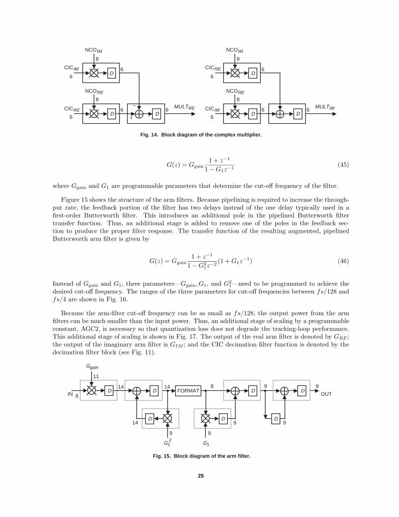
G(z) = Ggain1 + z−1
1−G1z−1(45)
where Ggain and G1 are programmable parameters that determine the cut-off frequency of the filter.
Figure 15 shows the structure of the arm filters. Because pipelining is required to increase the through-put rate, the feedback portion of the filter has two delays instead of the one delay typically used in afirst-order Butterworth filter. This introduces an additional pole in the pipelined Butterworth filtertransfer function. Thus, an additional stage is added to remove one of the poles in the feedback sec-tion to produce the proper filter response. The transfer function of the resulting augmented, pipelinedButterworth arm filter is given by
G(z) = Ggain1 + z−1
1−G21z−2
(1 +G1z−1) (46)
Instead of Ggain and G1, three parameters—Ggain, G1, and G21—need to be programmed to achieve the
desired cut-off frequency. The ranges of the three parameters for cut-off frequencies between fs/128 andfs/4 are shown in Fig. 16.
Because the arm-filter cut-off frequency can be as small as fs/128, the output power from the armfilters can be much smaller than the input power. Thus, an additional stage of scaling by a programmableconstant, AGC2, is necessary so that quantization loss does not degrade the tracking-loop performance.This additional stage of scaling is shown in Fig. 17. The output of the real arm filter is denoted by GRE ;the output of the imaginary arm filter is GIM ; and the CIC decimation filter function is denoted by thedecimation filter block (see Fig. 11).
14
Ggain
D
11
IN
D
9
6
14D
14D
FORMAT D D
D
9 9
OUT
9 9
9 9
G12
G1
Fig. 15. Block diagram of the arm filter.
25
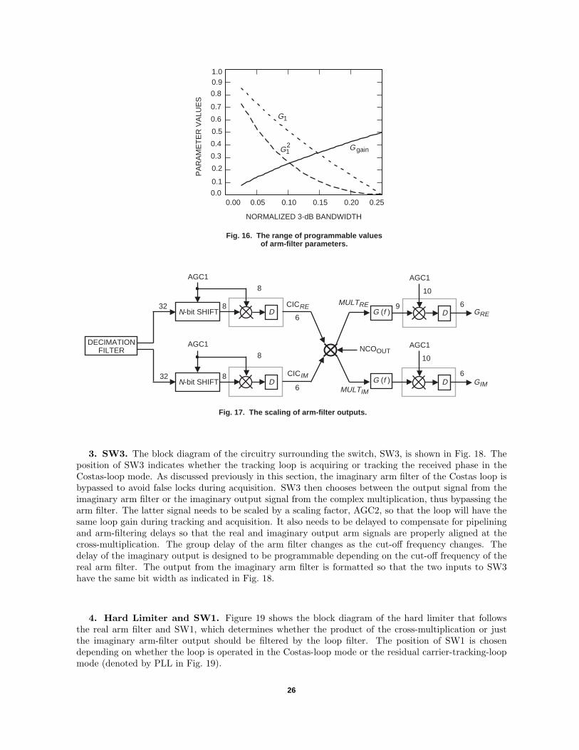
0.00 0.05 0.10 0.15 0.20 0.250.0
0.1
0.2
0.3
0.4
0.5
0.6
0.7
0.8
0.91.0
G12 G gain
G1
NORMALIZED 3-dB BANDWIDTH
PA
RA
ME
TE
R V
ALU
ES
Fig. 16. The range of programmable valuesof arm-filter parameters.
N-bit SHIFT D
D
DECIMATIONFILTER
32
32
AGC1
N-bit SHIFT8
8
8
8
6
6
10
10
9
AGC1
CICRE
6
CICIMD
D
AGC1
AGC1
6
GRE
GIMG (f )
NCOOUT
G (f )
MULTIM
MULTRE
Fig. 17. The scaling of arm-filter outputs.
3. SW3. The block diagram of the circuitry surrounding the switch, SW3, is shown in Fig. 18. Theposition of SW3 indicates whether the tracking loop is acquiring or tracking the received phase in theCostas-loop mode. As discussed previously in this section, the imaginary arm filter of the Costas loop isbypassed to avoid false locks during acquisition. SW3 then chooses between the output signal from theimaginary arm filter or the imaginary output signal from the complex multiplication, thus bypassing thearm filter. The latter signal needs to be scaled by a scaling factor, AGC2, so that the loop will have thesame loop gain during tracking and acquisition. It also needs to be delayed to compensate for pipeliningand arm-filtering delays so that the real and imaginary output arm signals are properly aligned at thecross-multiplication. The group delay of the arm filter changes as the cut-off frequency changes. Thedelay of the imaginary output is designed to be programmable depending on the cut-off frequency of thereal arm filter. The output from the imaginary arm filter is formatted so that the two inputs to SW3have the same bit width as indicated in Fig. 18.
4. Hard Limiter and SW1. Figure 19 shows the block diagram of the hard limiter that followsthe real arm filter and SW1, which determines whether the product of the cross-multiplication or justthe imaginary arm-filter output should be filtered by the loop filter. The position of SW1 is chosendepending on whether the loop is operated in the Costas-loop mode or the residual carrier-tracking-loopmode (denoted by PLL in Fig. 19).
26
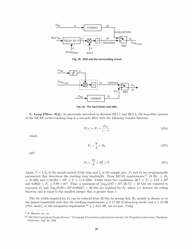
DELAY BY N6 10
10
SW3
D
AGC2
G IM Costas
MULTIM
TRACKING
6
FORMAT
ACQUISITION
6GIM
10
Fig. 18. SW3 and the surrounding circuit.
6
Groupdelay
D
10
10SW1
G IM Costas COSTAS
FORMAT
G RE
PLL
10G in
G IM
2
Fig. 19. The hard limiter and SW1.
5. Loop Filter: F(z). As previously described in Sections III.5.1 and III.5.2, the loop-filter portionof the MCAS carrier-tracking loop is a one-pole filter with the following transfer function:
F (z) = F1 +F2z
z − 1(47a)
where
F1 =83×BL (47b)
and
F2 =329×B2
L × T (47c)
Again, T = 1/fs is the sample period of the loop and fs is the sample rate. F1 and F2 are programmableparameters that determine the tracking loop bandwidth. From MCAS requirements,21 10 Hz ≤ BL≤ 10 kHz and 1/16.384 × 106 ≤ T ≤ 1/4/1000. Under these two conditions, 26.7 ≤ F1 ≤ 2.67 × 10⁴
and 0.0022 ≤ F2 ≤ 8.89 × 10⁴. Thus, a minimum of⌈log2(2.67× 10⁴/26.7)
⌉= 10 bits are required to
represent F1 and⌈log2(8.89× 10⁴/0.0022)
⌉= 26 bits are required for F2, where dxe denotes the ceiling
function and is equal to the smallest integer that is greater than x.
The bit width required for F2 can be reduced from 26 bits by noting that BL usually is chosen to bethe largest bandwidth such that the tracking requirements, ρ ≥ 17 dB (Costas-loop mode) and ρ ≥ 12 dB(PLL mode), or the navigation requirement,22 ρ ≥ 24.5 dB, can be met. Using
21 D. Hansen, op. cit.22 “MCAS1 Conceptual Design Review,” Viewgraph Presentation (internal document), Jet Propulsion Laboratory, Pasadena,
California, July 30, 1998.
27
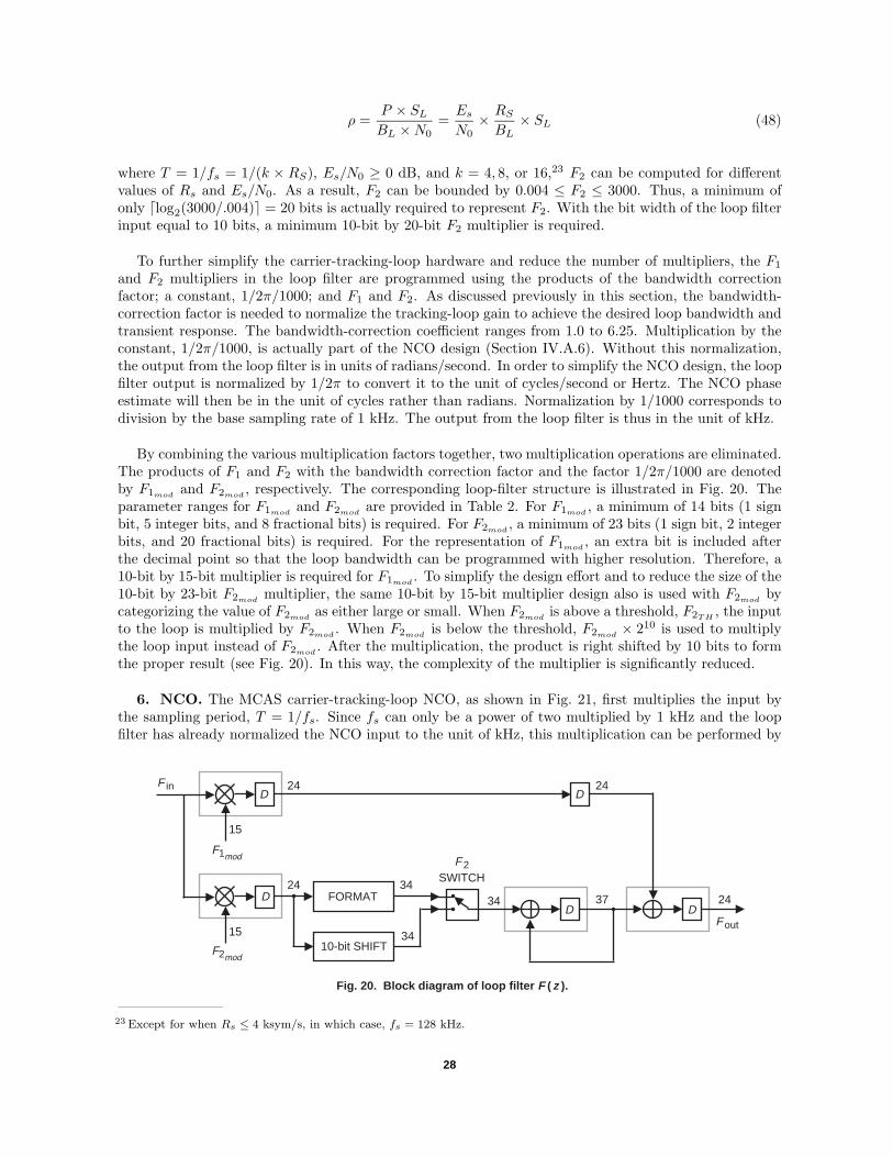
ρ =P × SLBL ×N0
=EsN0× RSBL× SL (48)
where T = 1/fs = 1/(k × RS), Es/N0 ≥ 0 dB, and k = 4, 8, or 16,23 F2 can be computed for differentvalues of Rs and Es/N0. As a result, F2 can be bounded by 0.004 ≤ F2 ≤ 3000. Thus, a minimum ofonly dlog2(3000/.004)e = 20 bits is actually required to represent F2. With the bit width of the loop filterinput equal to 10 bits, a minimum 10-bit by 20-bit F2 multiplier is required.
To further simplify the carrier-tracking-loop hardware and reduce the number of multipliers, the F1
and F2 multipliers in the loop filter are programmed using the products of the bandwidth correctionfactor; a constant, 1/2π/1000; and F1 and F2. As discussed previously in this section, the bandwidth-correction factor is needed to normalize the tracking-loop gain to achieve the desired loop bandwidth andtransient response. The bandwidth-correction coefficient ranges from 1.0 to 6.25. Multiplication by theconstant, 1/2π/1000, is actually part of the NCO design (Section IV.A.6). Without this normalization,the output from the loop filter is in units of radians/second. In order to simplify the NCO design, the loopfilter output is normalized by 1/2π to convert it to the unit of cycles/second or Hertz. The NCO phaseestimate will then be in the unit of cycles rather than radians. Normalization by 1/1000 corresponds todivision by the base sampling rate of 1 kHz. The output from the loop filter is thus in the unit of kHz.
By combining the various multiplication factors together, two multiplication operations are eliminated.The products of F1 and F2 with the bandwidth correction factor and the factor 1/2π/1000 are denotedby F1mod and F2mod , respectively. The corresponding loop-filter structure is illustrated in Fig. 20. Theparameter ranges for F1mod and F2mod are provided in Table 2. For F1mod , a minimum of 14 bits (1 signbit, 5 integer bits, and 8 fractional bits) is required. For F2mod , a minimum of 23 bits (1 sign bit, 2 integerbits, and 20 fractional bits) is required. For the representation of F1mod , an extra bit is included afterthe decimal point so that the loop bandwidth can be programmed with higher resolution. Therefore, a10-bit by 15-bit multiplier is required for F1mod . To simplify the design effort and to reduce the size of the10-bit by 23-bit F2mod multiplier, the same 10-bit by 15-bit multiplier design also is used with F2mod bycategorizing the value of F2mod as either large or small. When F2mod is above a threshold, F2TH , the inputto the loop is multiplied by F2mod . When F2mod is below the threshold, F2mod × 210 is used to multiplythe loop input instead of F2mod . After the multiplication, the product is right shifted by 10 bits to formthe proper result (see Fig. 20). In this way, the complexity of the multiplier is significantly reduced.
6. NCO. The MCAS carrier-tracking-loop NCO, as shown in Fig. 21, first multiplies the input bythe sampling period, T = 1/fs. Since fs can only be a power of two multiplied by 1 kHz and the loopfilter has already normalized the NCO input to the unit of kHz, this multiplication can be performed by
15
D
F1mod
10-bit SHIFT15
D
F2mod
F in
24FORMAT
34
34
D34 37
D24
F out
D24 24
F 2SWITCH
Fig. 20. Block diagram of loop filter F ( z ).
23 Except for when Rs ≤ 4 ksym/s, in which case, fs = 128 kHz.
28
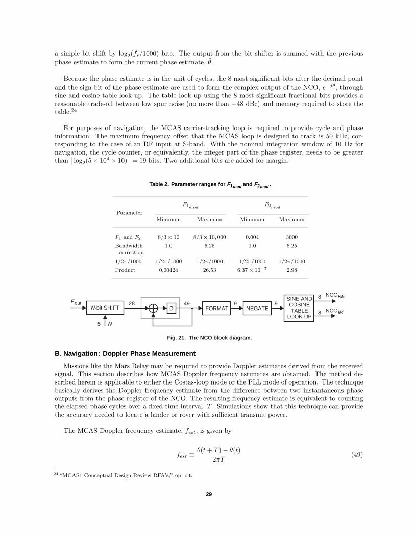
a simple bit shift by log2(fs/1000) bits. The output from the bit shifter is summed with the previousphase estimate to form the current phase estimate, θ̂.
Because the phase estimate is in the unit of cycles, the 8 most significant bits after the decimal pointand the sign bit of the phase estimate are used to form the complex output of the NCO, e−jθ̂, throughsine and cosine table look up. The table look up using the 8 most significant fractional bits provides areasonable trade-off between low spur noise (no more than −48 dBc) and memory required to store thetable.24
For purposes of navigation, the MCAS carrier-tracking loop is required to provide cycle and phaseinformation. The maximum frequency offset that the MCAS loop is designed to track is 50 kHz, cor-responding to the case of an RF input at S-band. With the nominal integration window of 10 Hz fornavigation, the cycle counter, or equivalently, the integer part of the phase register, needs to be greaterthan
⌈log2(5× 104 × 10)
⌉= 19 bits. Two additional bits are added for margin.
Table 2. Parameter ranges for F1mod and F2mod .
F1modF2mod
ParameterMinimum Maximum Minimum Maximum
F1 and F2 8/3× 10 8/3× 10, 000 0.004 3000
Bandwidth 1.0 6.25 1.0 6.25correction
1/2π/1000 1/2π/1000 1/2π/1000 1/2π/1000 1/2π/1000
Product 0.00424 26.53 6.37× 10⁻⁷ 2.98
5
N-bit SHIFT9
FORMATD49F out 28
N
9NEGATE
SINE ANDCOSINETABLE
LOOK-UP
NCORE8
8 NCOIM
Fig. 21. The NCO block diagram.
B. Navigation: Doppler Phase Measurement
Missions like the Mars Relay may be required to provide Doppler estimates derived from the receivedsignal. This section describes how MCAS Doppler frequency estimates are obtained. The method de-scribed herein is applicable to either the Costas-loop mode or the PLL mode of operation. The techniquebasically derives the Doppler frequency estimate from the difference between two instantaneous phaseoutputs from the phase register of the NCO. The resulting frequency estimate is equivalent to countingthe elapsed phase cycles over a fixed time interval, T . Simulations show that this technique can providethe accuracy needed to locate a lander or rover with sufficient transmit power.
The MCAS Doppler frequency estimate, fest, is given by
fest ≡θ(t+ T )− θ(t)
2πT(49)
24 “MCAS1 Conceptual Design Review RFA’s,” op. cit.
29
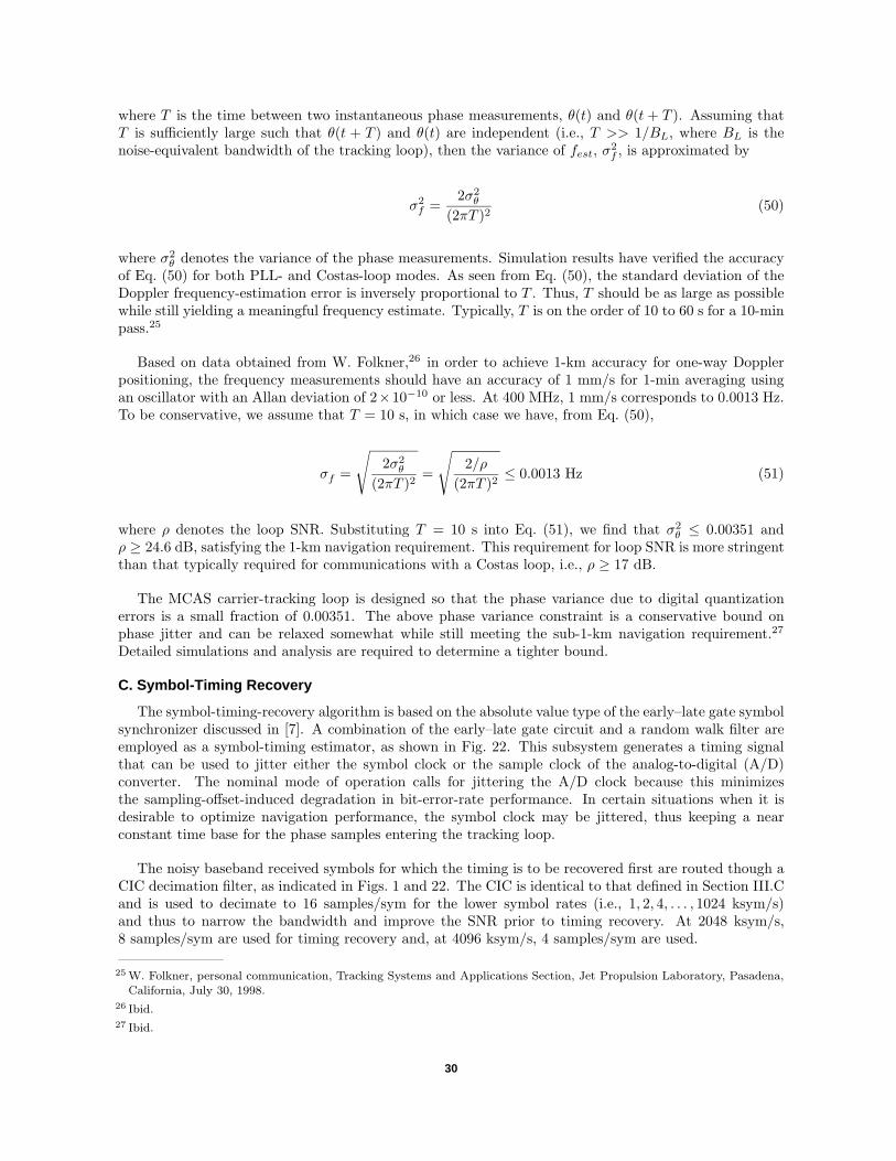
where T is the time between two instantaneous phase measurements, θ(t) and θ(t + T ). Assuming thatT is sufficiently large such that θ(t + T ) and θ(t) are independent (i.e., T >> 1/BL, where BL is thenoise-equivalent bandwidth of the tracking loop), then the variance of fest, σ2
f , is approximated by
σ2f =
2σ2θ
(2πT )2(50)
where σ2θ denotes the variance of the phase measurements. Simulation results have verified the accuracy
of Eq. (50) for both PLL- and Costas-loop modes. As seen from Eq. (50), the standard deviation of theDoppler frequency-estimation error is inversely proportional to T . Thus, T should be as large as possiblewhile still yielding a meaningful frequency estimate. Typically, T is on the order of 10 to 60 s for a 10-minpass.25
Based on data obtained from W. Folkner,26 in order to achieve 1-km accuracy for one-way Dopplerpositioning, the frequency measurements should have an accuracy of 1 mm/s for 1-min averaging usingan oscillator with an Allan deviation of 2×10⁻¹⁰ or less. At 400 MHz, 1 mm/s corresponds to 0.0013 Hz.To be conservative, we assume that T = 10 s, in which case we have, from Eq. (50),
σf =
√2σ2
θ
(2πT )2=
√2/ρ
(2πT )2≤ 0.0013 Hz (51)
where ρ denotes the loop SNR. Substituting T = 10 s into Eq. (51), we find that σ2θ ≤ 0.00351 and
ρ ≥ 24.6 dB, satisfying the 1-km navigation requirement. This requirement for loop SNR is more stringentthan that typically required for communications with a Costas loop, i.e., ρ ≥ 17 dB.
The MCAS carrier-tracking loop is designed so that the phase variance due to digital quantizationerrors is a small fraction of 0.00351. The above phase variance constraint is a conservative bound onphase jitter and can be relaxed somewhat while still meeting the sub-1-km navigation requirement.27
Detailed simulations and analysis are required to determine a tighter bound.
C. Symbol-Timing Recovery
The symbol-timing-recovery algorithm is based on the absolute value type of the early–late gate symbolsynchronizer discussed in [7]. A combination of the early–late gate circuit and a random walk filter areemployed as a symbol-timing estimator, as shown in Fig. 22. This subsystem generates a timing signalthat can be used to jitter either the symbol clock or the sample clock of the analog-to-digital (A/D)converter. The nominal mode of operation calls for jittering the A/D clock because this minimizesthe sampling-offset-induced degradation in bit-error-rate performance. In certain situations when it isdesirable to optimize navigation performance, the symbol clock may be jittered, thus keeping a nearconstant time base for the phase samples entering the tracking loop.
The noisy baseband received symbols for which the timing is to be recovered first are routed though aCIC decimation filter, as indicated in Figs. 1 and 22. The CIC is identical to that defined in Section III.Cand is used to decimate to 16 samples/sym for the lower symbol rates (i.e., 1, 2, 4, . . . , 1024 ksym/s)and thus to narrow the bandwidth and improve the SNR prior to timing recovery. At 2048 ksym/s,8 samples/sym are used for timing recovery and, at 4096 ksym/s, 4 samples/sym are used.
25 W. Folkner, personal communication, Tracking Systems and Applications Section, Jet Propulsion Laboratory, Pasadena,California, July 30, 1998.
26 Ibid.27 Ibid.
30

Ps (t - 2e)
FREE-RUNNINGSYMBOLCLOCK
EARLY-GATEACCUMULATOR
ON-TIMEACCUMULATOR
LATE-GATEACCUMULATOR
ERRORACCUMULATOR
THRESHOLDCIRCUIT
INPUT
CICFILTER
DELAYe
Ps (t )
Ps (t - e)DELAY
2e
MATCHEDFILTEREDSYMBOLS
+1-1
+1-1
S
+
-
FREE-RUNNINGSAMPLECLOCK
TO A/D16.384 MHz
32.768-MHzREFERENCEOSCILLATOR
ERR > C ERR > -C
RETARDCLOCK 1SAMPLE
RETARDCLOCK 1SAMPLE
Fig. 22. Block diagram of the symbol-timing estimator.
ERR
The early–late gate symbol-synchronization algorithm is motivated by the maximum a posteriori(MAP) estimation of an unknown parameter in Gaussian noise. As with the MAP estimator, the re-ceived BPSK signal that has passed through the CIC first is routed to cross-correlators. The correlatorsoperate on three different subintervals of the received signal (i.e., early, late, and on time), multiplying thereceived signal by an appropriately delayed stored replica of the transmitted pulse and then integrating(see Fig. 22).
The nominal operating mode of the symbol-timing-recovery circuit corresponds to NRZ pulse shaping,in which case the pulse shape depicted in Fig. 22 is Ps(t) = 1. In the case of the Manchester-encodedpulse shape, a stored replica of the Manchester Ps(t) (a binary 1 is represented as a 1 for the first half ofthe symbol period and a 0 for the second half of the symbol period) is multiplied by the received signalfor each of the three arms of the timing recovery circuit.
The multiplications by the pulse shape are followed by an early integrator, an on-time integrator, anda late integrator. The three integrators are controlled by synchronous clocks that are slightly offset intime. The integration period is Ts for all three integrate-and-dump channels, with the early integrationstarting a quarter of a symbol early and the late integration starting a quarter of a symbol late (i.e.,ε = Ts/4 in Fig. 22, which is shown to be optimal in [7]). The on-time integration is equivalent to amatched filter for the transmitted symbols when the symbol timing is perfectly aligned.
The outputs from the early and late integrators are utilized to generate a timing-error signal bydifferencing their respective absolute values. If the value of the early channel is greater that than that ofthe late channel, an error signal is generated that slows down the clock and, if the late channel value is
31
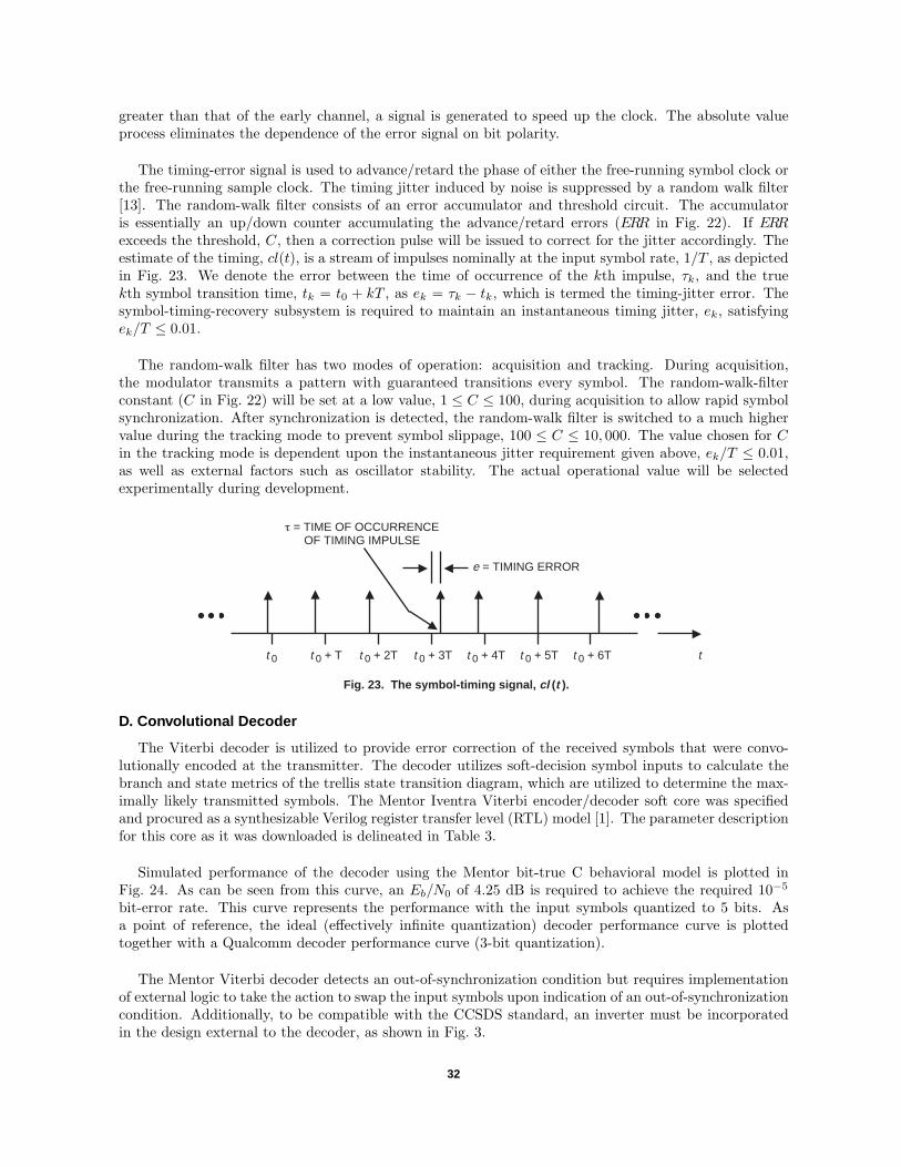
greater than that of the early channel, a signal is generated to speed up the clock. The absolute valueprocess eliminates the dependence of the error signal on bit polarity.
The timing-error signal is used to advance/retard the phase of either the free-running symbol clock orthe free-running sample clock. The timing jitter induced by noise is suppressed by a random walk filter[13]. The random-walk filter consists of an error accumulator and threshold circuit. The accumulatoris essentially an up/down counter accumulating the advance/retard errors (ERR in Fig. 22). If ERRexceeds the threshold, C, then a correction pulse will be issued to correct for the jitter accordingly. Theestimate of the timing, cl(t), is a stream of impulses nominally at the input symbol rate, 1/T , as depictedin Fig. 23. We denote the error between the time of occurrence of the kth impulse, τk, and the truekth symbol transition time, tk = t0 + kT , as ek = τk − tk, which is termed the timing-jitter error. Thesymbol-timing-recovery subsystem is required to maintain an instantaneous timing jitter, ek, satisfyingek/T ≤ 0.01.
The random-walk filter has two modes of operation: acquisition and tracking. During acquisition,the modulator transmits a pattern with guaranteed transitions every symbol. The random-walk-filterconstant (C in Fig. 22) will be set at a low value, 1 ≤ C ≤ 100, during acquisition to allow rapid symbolsynchronization. After synchronization is detected, the random-walk filter is switched to a much highervalue during the tracking mode to prevent symbol slippage, 100 ≤ C ≤ 10, 000. The value chosen for Cin the tracking mode is dependent upon the instantaneous jitter requirement given above, ek/T ≤ 0.01,as well as external factors such as oscillator stability. The actual operational value will be selectedexperimentally during development.
t 0 t 0 + T t 0 + 2T t 0 + 3T t 0 + 4T t 0 + 5T t 0 + 6T t
e = TIMING ERROR
t = TIME OF OCCURRENCEOF TIMING IMPULSE
Fig. 23. The symbol-timing signal, cl (t ).
D. Convolutional Decoder
The Viterbi decoder is utilized to provide error correction of the received symbols that were convo-lutionally encoded at the transmitter. The decoder utilizes soft-decision symbol inputs to calculate thebranch and state metrics of the trellis state transition diagram, which are utilized to determine the max-imally likely transmitted symbols. The Mentor Iventra Viterbi encoder/decoder soft core was specifiedand procured as a synthesizable Verilog register transfer level (RTL) model [1]. The parameter descriptionfor this core as it was downloaded is delineated in Table 3.
Simulated performance of the decoder using the Mentor bit-true C behavioral model is plotted inFig. 24. As can be seen from this curve, an Eb/N0 of 4.25 dB is required to achieve the required 10−5
bit-error rate. This curve represents the performance with the input symbols quantized to 5 bits. Asa point of reference, the ideal (effectively infinite quantization) decoder performance curve is plottedtogether with a Qualcomm decoder performance curve (3-bit quantization).
The Mentor Viterbi decoder detects an out-of-synchronization condition but requires implementationof external logic to take the action to swap the input symbols upon indication of an out-of-synchronizationcondition. Additionally, to be compatible with the CCSDS standard, an inverter must be incorporatedin the design external to the decoder, as shown in Fig. 3.
32
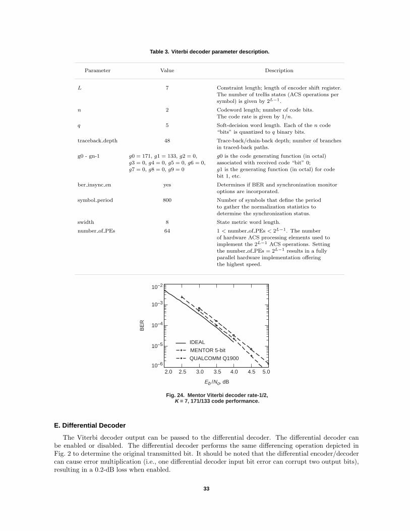
Table 3. Viterbi decoder parameter description.
Parameter Value Description
L 7 Constraint length; length of encoder shift register.The number of trellis states (ACS operations persymbol) is given by 2L−1.
n 2 Codeword length; number of code bits.The code rate is given by 1/n.
q 5 Soft-decision word length. Each of the n code“bits” is quantized to q binary bits.
traceback depth 48 Trace-back/chain-back depth; number of branchesin traced-back paths.
g0 - gn-1 g0 = 171, g1 = 133, g2 = 0, g0 is the code generating function (in octal)g3 = 0, g4 = 0, g5 = 0, g6 = 0, associated with received code “bit” 0;g7 = 0, g8 = 0, g9 = 0 g1 is the generating function (in octal) for code
bit 1, etc.
ber insync en yes Determines if BER and synchronization monitoroptions are incorporated.
symbol period 800 Number of symbols that define the periodto gather the normalization statistics todetermine the synchronization status.
swidth 8 State metric word length.
number of PEs 64 1 < number of PEs < 2L−1. The numberof hardware ACS processing elements used toimplement the 2L−1 ACS operations. Settingthe number of PEs = 2L−1 results in a fullyparallel hardware implementation offeringthe highest speed.
2.0 2.5 3.0 3.5 4.0 4.5 5.010-6
10-5
10-4
10-3
10-2
IDEAL
MENTOR 5-bit
QUALCOMM Q1900
Eb /No, dB
BE
R
Fig. 24. Mentor Viterbi decoder rate-1/2,K = 7, 171/133 code performance.
E. Differential Decoder
The Viterbi decoder output can be passed to the differential decoder. The differential decoder canbe enabled or disabled. The differential decoder performs the same differencing operation depicted inFig. 2 to determine the original transmitted bit. It should be noted that the differential encoder/decodercan cause error multiplication (i.e., one differential decoder input bit error can corrupt two output bits),resulting in a 0.2-dB loss when enabled.
33
F. Descrambler
The descrambler follows the differential decoder in the receive chain and can be enabled or disabled.The descrambler is discussed in Section II. It should be noted that descrambling can cause error multi-plication and that the Mentor Graphics implementation of the descrambler incurs a 0.3-dB loss when thescrambling/descrambling is enabled.
V. Summary
This article has provided a detailed overview of the MCAS1 communications system, including thedigital design considerations leading to a low-mass and -power transceiver. The system is being de-signed to operate over a wide range of data rates from 1 kb/s to 4 Mb/s and must accommodate fre-quency uncertainties up to 10 kHz with navigational Doppler tracking capabilities. As such, the designis highly programmable and incorporates efficient front-end digital decimation architectures to mini-mize power-consumption requirements. MCAS1 implements most of its transceiver functions with digitalFPGA/ASIC technology. This leaves just the RF upconversion and downconversion to be implementedin the analog domain. The approach with the RF subsystem design is to use space-qualified parts whenavailable and leverage the large investment that industry has made in developing highly integrated devicesfor the commercial wireless markets. The ultimate goal of the MCAS communications effort is to enablereliable communications at a significant mass, power, size, and cost reduction and for a broad class ofvery small platforms requiring short-range communications.
References
[1] “Viterbi Encoder/Decoder Technical Product Brief,” Mentor Graphics Corp.,1997.
[2] “Harris Digital Costas Loop HSP50210 Product Description,” File No. 3652.2,Harris Corp., 1996.
[3] Deep Space Telecommunications Systems Engineering, J. Yuen, Ed., New York:Plenum Press, 1983.
[4] “Analog Devices AD9200 Specification Sheet,” Analog Devices, Inc., 1998.
[5] E. Hogenauer, “An Economical Class of Digital Filters for Decimation and In-terpolation,” IEEE Transactions on Acoustics, Speech, and Signal Processing,vol. 34, pp. 155–162, April 1981.
[6] A. Kwentus, Z. Jiang, and A. Willson, “Application of Filter Sharpening toCascaded Integrator-Comb Decimation Filters,” IEEE Transactions on SignalProcessing, vol. 45, pp. 457–467, February 1997.
[7] W. Lindsey and M. Simon, Telecommunication Systems Engineering, EnglewoodCliffs, New Jersey: Prentice Hall, 1973.
[8] M. Simon and W. Lindsey, “Optimum Performance of Suppressed-Carrier Re-ceivers With Costas Loop Tracking,” IEEE Trans. on Comm., vol. COM-25,no. 2, pp. 215–227, February 1977.
[9] M. Simon, “Tracking Performance of Costas Loops With Hard-Limited In-PhaseChannel,” IEEE Trans. on Comm., vol. COM-26, no. 4, pp. 420–432, April 1978.
34
[10] S. Aguirre and W. J. Hurd, “Design and Performance of Sampled Data Loopsfor Subcarrier and Carrier Tracking,”The Telecommunications and Data Acqui-sition Progress Report 42-79, July–September 1984, Jet Propulsion Laboratory,Pasadena, California, pp. 81–95, November 15, 1984.http://tmo.jpl.nasa.gov/tmo/progress report/42-79/79H.PDF
[11] M. Simon, “The False Lock Performance of Costas Loops With Hard-Limited In-Phase Channel,” IEEE Transactions On Communications, vol. VOM-26, no. 1,January 1978.
[12] C. Cahn, “Improving Frequency Acquisition of a Costas Loop,” IEEE Transac-tions On Communications, vol. COM-25, no. 12, December 1977.
[13] D. Paranchych and N. Beaulieu, “Use of Second Order Markov Chains to ModelDigital Symbol Synchroniser Performance,” IEE Proc.–Commun., vol. 143, no. 5,October 1996.
[14] H. Meyr and G. Ascheid, Synchronization in Digital Communications, vol. 1,New York: Wiley & Sons, 1990.
35