
1 Micro-fabrication Process. 2 Clean Room 3 Clean room classifications and applications.
Micro and Nanofabrication Clean Room Techniques and equipment
TECHNIQUES
• Metal and dielectric wet (isotropic) etching • Surface cleaning • Photoresist stripping: oxygen plasma and wet stripping
EQUIPMENT
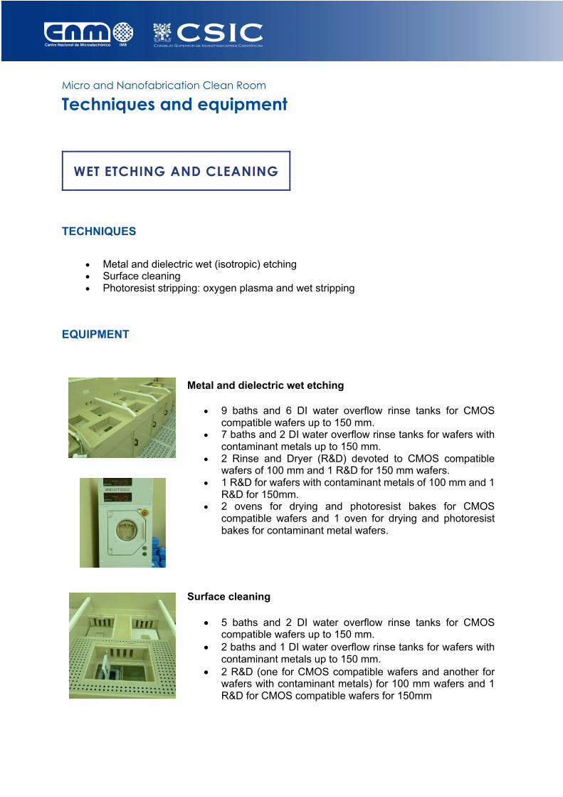
Metal and dielectric wet etching
• 9 baths and 6 DI water overflow rinse tanks for CMOS compatible wafers up to 150 mm.
• 7 baths and 2 DI water overflow rinse tanks for wafers with contaminant metals up to 150 mm.
• 2 Rinse and Dryer (R&D) devoted to CMOS compatible wafers of 100 mm and 1 R&D for 150 mm wafers.
• 1 R&D for wafers with contaminant metals of 100 mm and 1 R&D for 150mm.
• 2 ovens for drying and photoresist bakes for CMOS compatible wafers and 1 oven for drying and photoresist bakes for contaminant metal wafers.
Surface cleaning
• 5 baths and 2 DI water overflow rinse tanks for CMOS compatible wafers up to 150 mm.
• 2 baths and 1 DI water overflow rinse tanks for wafers with contaminant metals up to 150 mm.
• 2 R&D (one for CMOS compatible wafers and another for wafers with contaminant metals) for 100 mm wafers and 1 R&D for CMOS compatible wafers for 150mm
WET ETCHING AND CLEANING

• A Sirius Semitool equipment for cleanings based on O3 and hot water spray for CMOS compatible wafers up to 150mm
Wet and oxygen plasma photoresist stripping
• 1 double ultrasonic bath for solvents and 1 DI water overflow rinse tank for CMOS compatible wafers.
• 2 baths for wet photoresist stripping for wafers with contaminant metals and 1 DI water overflow rinse tank for wafers with contaminant metals up to 150 mm.
• PVA Tepla 300SA plasma asher for photoresist stripping with oxygen plasma for CMOS compatible wafers.
• Tepla GIGABatch 360M plasma asher for photoresist stripping with oxygen plasma for wafers with contaminant metals up to 150mm.
PROCESSES
Ething and stripping of dielectrics
• Etching and stripping of SiO2 in HF mixtures of different concentrations.
• Isotropic etching of silicon and polysilicon based on mixtures of HNO3 y HF.
• Etching of Si3N4 in H3PO4 • Thin film etching of TiO2and HfO2 in HF mixtures. • Thin film etching of Al2O3 based on mixtures of HNO3 and
H3PO4.
Etching of metals
• Al etching based on mixtures of HNO3 y H3PO4 • Au etching based on mixtures of I2 • Ni etching in HNO3 • Ti etching based on mixtures of propilenglycol and HF
Surface cleanings

Cleaning of organics, particles and remaining traces of metallic (ionic) contaminants in:
• Piranha mixture, oxide stripping and RCA cleaning. • Cleanings with solvents (acetone and isopropanol). • O3 and hot water spray based cleaning
Wet and oxygen plasma photoresist stripping
• Photoresist stripping in acetone. • Photoresist stripping in acid. • Photoresist stripping in stripper (basic mixture). • Photoresist stripping in oxygen plasma.
STAFF:
• Nuria Torres • Elena Chica • Andrea Azambuja


