Micro adc notes - College of Engineering€¦ · The PIC MCU will then automatically be interrupted...
35
KHAN WAHID 2009-10 (Term 1) EE331 Microprocessor Notes on ADC and PWM Notes on ADC and PWM (PIC16F Family) (PIC16F Family)
Transcript of Micro adc notes - College of Engineering€¦ · The PIC MCU will then automatically be interrupted...
KHAN WAHID 2009-10 (Term 1)
EE331 Microprocessor
Notes on ADC and PWM Notes on ADC and PWM (PIC16F Family)(PIC16F Family)

Dr. KHAN WAHID2009-10 (Term 1)
2EE 331: Microprocessor
16F886 ArchitectureExactly same architecture as 16F84A
Same 35 instructionsAll single cycle except program branches (2-cycles)
Brown-out ResetIn-Circuit DebuggerLow-volt Programming

Dr. KHAN WAHID2009-10 (Term 1)
3EE 331: Microprocessor
16F886 Status Register
The data memory is partitioned into four banks which contain the GPR and the SFREach bank extends up to 7Fh (128 bytes)
The lower locations of each bank are reserved for the SFRThe GPR are implemented as static RAM

Dr. KHAN WAHID2009-10 (Term 1)
4EE 331: Microprocessor
Configuring PORTAWhen ports are multiplexed, take special caution to configure
- On reset, all PORTA pins are analog and read as ‘0’- To use them as digital, we must configure ADCON1
ADCON1

Dr. KHAN WAHID2009-10 (Term 1)
5EE 331: Microprocessor
Configuring PORTA – for 16F886However, it may not be always trivial from the datasheet
- Here, we need to configure ANSEL
- However, there are still problems with RA6 and RA7- Since they are multiplexed with OSC1 and OSC2 respectively, we must configure the “Configuration Bits”
“Setting the appropriate ANSEL bit high will cause all digital reads on the pin to be read as ‘0’ and allow analog functions on the pin to operate correctly. The state of the ANSEL bits has no affect on digital output functions. A pin with TRIS clear and ANSEL set will still operate as a digital output, but the Input mode will be analog. This can cause unexpected behavior when executing read-modify-write instructions (e.g., bsf, bcf) on the affected port.

Dr. KHAN WAHID2009-10 (Term 1)
6EE 331: Microprocessor
Configuring PORTA/PORTB – for 16F886Port B is also multiplexed
Need to be cautious
- Here, we need to configure ANSELH
Demo in MPLAB
Dr. KHAN WAHID2009-10 (Term 1)
7EE 331: Microprocessor
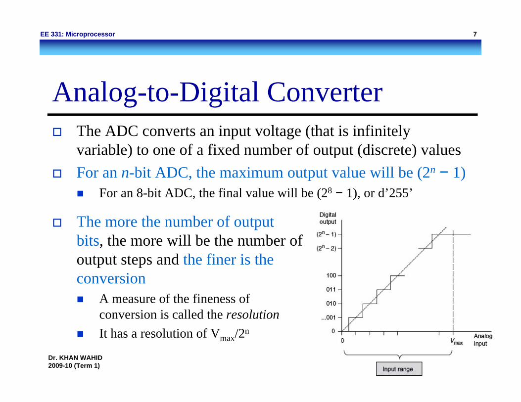
Analog-to-Digital ConverterThe ADC converts an input voltage (that is infinitely variable) to one of a fixed number of output (discrete) values For an n-bit ADC, the maximum output value will be (2n − 1)
For an 8-bit ADC, the final value will be (28 − 1), or d’255’
The more the number of output bits, the more will be the number of output steps and the finer is the conversion
A measure of the fineness of conversion is called the resolutionIt has a resolution of Vmax/2n

Dr. KHAN WAHID2009-10 (Term 1)
8EE 331: Microprocessor
Sample and HoldSince, an ADC cannot convert accurately a changing voltage, a sample and hold (S&H) circuit is often found
This takes a sample of the voltage, like a snapshot, and holds it steady for the duration of the conversionComposed of a semiconductor switch and a capacitor
Sample: When the switch is closed, the capacitor charges up to the input voltage Vs
Vo = Vc = VsHold: When the switch opens, the charge is left on the capacitor and Vc(and hence Vo) remains at a fixed value
Vc = Vs {1 − exp(−t/RC)}

Dr. KHAN WAHID2009-10 (Term 1)
9EE 331: Microprocessor
Sample and HoldThe time that Vc (and hence Vo) takes to reach a value deemed to be acceptable is called the acquisition time
Suppose that Vc must rise to 90% of its final value (Vs)
To ensure good accuracy in data conversion, the error introduced by this process should be less than the equivalent of half of 1 LSB
For an 8-bit conversion, this implies that the acquired voltage value Vc must reach ≥ (511/512)Vs, or 0.9980Vs
For a 10-bit conversion it must be ≥ (2047/2048)Vs, or 0.9995Vs
Vc = Vs {1 − exp(−t/RC)}

Dr. KHAN WAHID2009-10 (Term 1)
10EE 331: Microprocessor
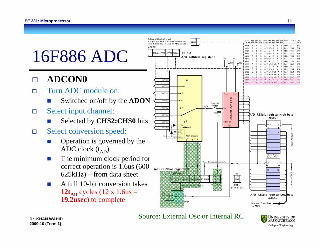
16F886 ADCPowerful 10-bit 8-channel ADC moduleThe ADC is controlled by: ADCON0 and ADCON1The result of the conversion is placed into: ADRESH and ADRESLOther SFRs also have an important impact on the ADC:
TRISA and TRISE (used for analog input)PIR1 and PIE1 contain the ADC INT flag and INT enable bits
A set of procedure must be followed to properly complete one conversion
Dr. KHAN WAHID2009-10 (Term 1)
11EE 331: Microprocessor
16F886 ADCADCON0Turn ADC module on:
Switched on/off by the ADONSelect input channel:
Selected by CHS2:CHS0 bitsSelect conversion speed:
Operation is governed by the ADC clock (tAD)The minimum clock period for correct operation is 1.6us (600-625kHz) – from data sheetA full 10-bit conversion takes12tAD cycles (12 x 1.6us = 19.2usec) to complete
Source: External Osc or Internal RC

Dr. KHAN WAHID2009-10 (Term 1)
12EE 331: Microprocessor
16F886 ADCADCON0
But, if the conversion is too slow, charge may leak from capacitor and conversion becomes inaccurateThe best practice is to set the ADC clock such that it has a period equal to or just less than 1.6usThere is also a dedicated RC oscillator (typical period of 4us, but may range from 2-6us
Configure input channelsBy the setting of bits PGFC3:PGFC0 of ADCON1

Dr. KHAN WAHID2009-10 (Term 1)
13EE 331: Microprocessor
16F886 ADCADCON1
The variety of opportunity is impressive, both in terms of input channels and voltage referenceFrom just a single Port A channel used for input (PGFC3:PGFC0 = 1110) to all eight analog inputs in play (PGFC3:PGFC0 = 0000)An external reference are also possibleNote again that any port pin that is to be used as an analog input must be set as an input in its TRIS register

Dr. KHAN WAHID2009-10 (Term 1)
14EE 331: Microprocessor
16F886 ADCStart the conversion
A conversion is initiated by setting bit GO/NOT_DONE When the conversion is complete the bit is returned to zero automatically (by the hardware)The completion is also signalledby an ADC interrupt flag ADIF(in PIR1)
Reading the resultsTwo possible result formats are possible (set by ADFM in ADCON1)

Dr. KHAN WAHID2009-10 (Term 1)
15EE 331: Microprocessor
16F886 ADCStart the conversion
A conversion is initiated by setting bit GO/NOT_DONE When the conversion is complete the bit is returned to zero automatically (by the hardware)The completion is also signalledby an ADC interrupt flag ADIF(in PIR1)
Reading the resultsTwo possible result formats are possible (set by ADFM in ADCON1)
Q. How about 8-bit?

Dr. KHAN WAHID2009-10 (Term 1)
16EE 331: Microprocessor
Acquisition and Conversion TimeThe best possible complete conversion time: 28.5usec (how?)
Typical acquisition: 17usecTypical conversion: 20usecTypical complete: 37usec
Repeated conversionWhen a conversion is complete, the converter waits for a period of 2tAD before it is available to start a new conversion cycleOnce this time is up, either the same input channel may be converted again, or a new one may selectedFor repeated conversion, the “best possible” complete conversion cycle time becomes 31.7usec (28.5 + 3.2)
This implies a maximum sampling rate of around 30 kHzNote, however, that this figure takes no account of software overheads, which would tend to slow the conversion rate

Dr. KHAN WAHID2009-10 (Term 1)
17EE 331: Microprocessor
ADC – Complete Process1. Configure ADC module
a) Set up port pins as analog/voltage reference (ADCON1) – PCFG3:PCFG0b) Select ADC conversion clock source (ADCON0) – ADCS1:ADCS0c) Select ADC input channel (ADCON0) – CH2:CH0d) Turn on ADC module (ADCON0) - ADON
2. Wait for the required acquisition time, typically 17-20usec3. Start conversion by setting the GO/NOT_DONE bit (ADCON0)4. Wait for ADC conversion to complete by polling the GO/NOT_DONE bit
for logic 0 (12tAD)
5. Read the ADRESH/L registers (depending on ADFM setting)
6. For next conversion, wait for 2tADand go to step 1 or step 2 as required

Dr. KHAN WAHID2009-10 (Term 1)
18EE 331: Microprocessor
16F886 ADC – ExampleScanning an 8-channel Data acquisition system
- The ADC module clock source as fOSC/32; i.e., 20/32 = 625 kHz or 1.6usec- A delay subroutine is called to allow for: switch delay + stabilization + acquisition - For 8-bit resolution:17usec

Dr. KHAN WAHID2009-10 (Term 1)
19EE 331: Microprocessor
Example – contd..
w <= b’00000xxx’
Can be used with any program
CHS2:CHS0 are in ADCON0[5:3]Changing positions of the control bits from [2:0] to [5:3] => w = b’00xxx000’
Must NOT change other bitsADCON0 = b’??000???’ + b’00xxx000’Polling GO bit => wait for GO to go ‘0’(conversion complete)
Read results; ADFM = 0, 8-bit res
ADCON0

Dr. KHAN WAHID2009-10 (Term 1)
20EE 331: Microprocessor
A/D Conversion in Sleep ModeSelf-study – pp. 460-461

Dr. KHAN WAHID2009-10 (Term 1)
21EE 331: Microprocessor
Capture/Compare/PWM (CCP)Two CCP modules in PIC16F886 Each Capture/Compare/PWM (CCP) module contains
A 16-bit Capture registerA 16-bit Compare registerA PWM Master/Slave Duty Cycle register
Each CCP module has an associated control register (CCP1CON, CCP2CON) to set the modeBoth CCP1 and CCP2 modules are virtually identical in operation
Bank0 Bank1
Dr. KHAN WAHID2009-10 (Term 1)
22EE 331: Microprocessor
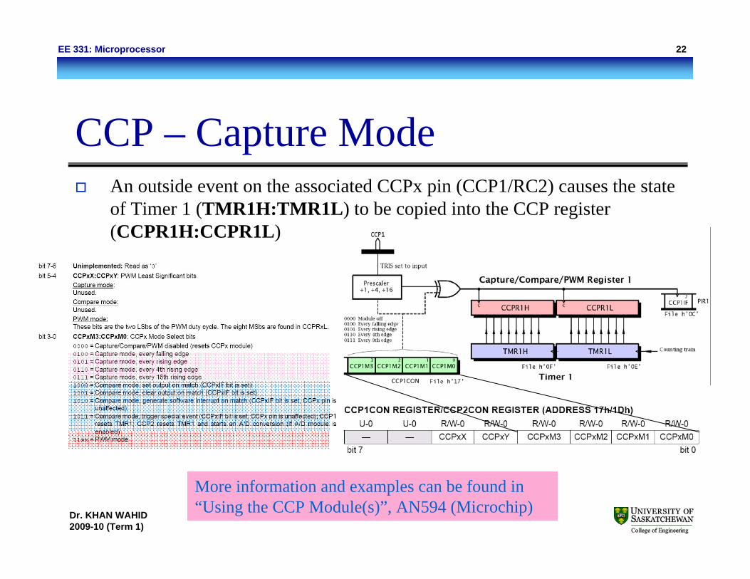
CCP – Capture ModeAn outside event on the associated CCPx pin (CCP1/RC2) causes the state of Timer 1 (TMR1H:TMR1L) to be copied into the CCP register (CCPR1H:CCPR1L)
More information and examples can be found in “Using the CCP Module(s)”, AN594 (Microchip)

Dr. KHAN WAHID2009-10 (Term 1)
23EE 331: Microprocessor
CCP – Capture ModeAn outside event on the associated CCPx pin (CCP1/RC2) causes the state of Timer 1 (TMR1H:TMR1L) to be copied into the CCP register (CCPR1H:CCPR1L)
The CCP2 module is the same, but there is no room for the CCP2Interrupt Flag CCP2IF and its associated CCP2IE mask bit in the PIR1/PIE1 registers. Instead PIR2[0] and PIE2[0] are used
Every time a capture occurs, the CCP1 Interrupt Flag (CCP1IF)is set in PIR1[2] and if the CCP1IE mask bit in PIE1[2] is set, an interrupt will be generated

Dr. KHAN WAHID2009-10 (Term 1)
24EE 331: Microprocessor
CCP – Compare ModeA digital equality comparator detects when the 16-bit Timer 1 data (TMR1H:TMR1L) equals the setting in the 16-bit CCPR1H:CCPR1L
When an equality match occurs, the CCP1IF interrupt flag in PIR1[2] will be set and this can cause an interrupt
TMR1 is auto reset at the same timeNote that, it is the same CCP1IF that would be set when capture occurs (in Capture mode)
Example: Consider that we wish to set up Timer 1 to overflow every 10 seconds (running at 32.768kHz).

Dr. KHAN WAHID2009-10 (Term 1)
25EE 331: Microprocessor
Example: CCP – Compare ModeConsider that we wish to set up Timer 1 to overflow every 10 seconds(running at 32.768kHz). To do this we need to set the timer to time-out after 16 s (when PS is 1:8 (max)) and then shorten the cycle. This is implemented by loading the CCPR1 register with the fraction 10/16 => 216 x 10/16 = h’A000’
Whenever Timer 1 reaches this value, it will automatically be reset and an interrupt will occur if the CCP1IE mask bit (and global PEIE and GIE masks) are set
The PIC MCU will then automatically be interrupted every 10 seconds
Task list:1. Load CCPR1 with h’A000’2. Configure CCP1CON3. Configure T1CON4. Enable CCP1, Peripherals,
GIE interrupts
How about TMR1 INT? => TMR1IF

Dr. KHAN WAHID2009-10 (Term 1)
26EE 331: Microprocessor
Timer 2 (TMR2) – 8-bits CounterTimer2 (TMR2) is different than Timer0 and Timer1Control register: T2CONHas both prescaler and postscalerNo external clock input is possible
Bank0 Bank1
ON/OFF

Dr. KHAN WAHID2009-10 (Term 1)
27EE 331: Microprocessor
Timer 2 (TMR2) – 8-bits CounterOutput is taken from TMR2 Comparator (not from TMR2)
This compares TMR2 with that in the Period Register (PR2)On equality, an output pulse is generated which resets TMR2 at the next count pulseAs determined by the Postscaler, any integer number from 1 to 16 of these reset events will set the Timer2 Interrupt Flag TMR2IF in PIR1[1]
Bank0 Bank1
Mainly used to generate hardwired PWM (with CCP module)

Dr. KHAN WAHID2009-10 (Term 1)
28EE 331: Microprocessor
Timer 2 (TMR2) – 8-bits CounterOutput is taken from TMR2 Comparator (not from TMR2)
This compares TMR2 with that in the Period Register (PR2)On equality, an output pulse is generated which resets TMR2 at the next count pulseAs determined by the Postscaler, any integer number from 1 to 16 of these reset events will set the Timer2 Interrupt Flag TMR2IF in PIR1[1]
PS=1:4

Dr. KHAN WAHID2009-10 (Term 1)
29EE 331: Microprocessor
CCP – PWM ModePWM is a very powerful technique that allows analog variables to be controlled from a digital output with just a single data connection
A PWM waveform generally has a fixed period with a variable pulse widthThe average amplitude is simply AxN, where N is the duty cycle fraction of the repeat periodIf we vary N from 0 to 100% then the average power will varyThis digital-to-analog conversion technique is known as pulse width modulation (PWM)

Dr. KHAN WAHID2009-10 (Term 1)
30EE 331: Microprocessor
CCP – PWM Mode (10-bit resolution)TMR2 + Prescale is used to implement period (10-bits)CCPR1L + CCP1CON[5:4]is used to set duty cycle (10-bits)
CCP1 is the PWM output
Both CCP modules can operate in parallel with different Duty numbers, but they share the same TMR2, thus have the same period

Dr. KHAN WAHID2009-10 (Term 1)
31EE 331: Microprocessor
CCP – PWM ModeEach time TMR2 overflows the Period number, three things happen (shown in red):
TMR2 is reset to zeroThe PWM latch is set and pin CCP1 goes to its High stateThe 10-bit content of the Master register is copied into the Slave register –this content is the duty number to the 10-bit PWM digital comparator
Period:

Dr. KHAN WAHID2009-10 (Term 1)
32EE 331: Microprocessor
CCP – PWM ModeDuty Cycle
2-stage 10-bit wide pipeline (why?)
The contents of the Master register can be altered at any time by the software using two separate movwfinstructions
The loaded word is onlymoved down the pipeline to be presented as the Duty number to the comparator at the end of each period –prevents mid-period glitch

Dr. KHAN WAHID2009-10 (Term 1)
33EE 331: Microprocessor
CCP – PWM ModeDuty Cycle
The Slave register comprises CCPR1H companded with a 2-bit internal latchIn this mode the CCPR1H register is read-only – this prevents direct access by software to the Duty numberThe CCP1IF is not altered in this mode (Compare, Capture)
Duty cycle = tosc x PS x {extended CCPR1H}

Dr. KHAN WAHID2009-10 (Term 1)
34EE 331: Microprocessor
PWM Initialization

Dr. KHAN WAHID2009-10 (Term 1)
35EE 331: Microprocessor
AcknowledgmentsThese slides have been prepared by Khan Wahid and may contain material copyrighted by:
The Quintessential PIC® Microcontroller, Sid Katzen, 2nd edition, 2005, ISBN: 978-1-85233-942-5Designing Embedded Systems with PIC Microcontrollers: Principles and Applications, Tim Wilmshurt, 2007, ISBN: 978-0750667555PIC16F87XA Data Sheet, 39582b, Microchip Technology Inc.PIC16F886 Data Sheet, 41291F, Microchip Technology Inc.