Metal Assisted Chemical and Electrochemical Etching...
59
Metal Assisted Chemical and Electrochemical Etching of Silicon Carl V. Thompson Materials Science and Engineering, MIT Faculty Collaborators: Wee-Kiong Choi, National University of Singapore Caroline Ross (MIT) Student Collaborators: Shie-Wei Chang (MIT, now Apple) Prayudi Lianto (NUS), Changquan Lai (NUS), Wen Zheng (MIT) • Basic mechanisms, making wire arrays, applications • The origin, impact, and control of excess holes in MACE (and ‘EMACE’) • Metal Assisted Anodic Etching (MAAE) • Separate roles of electrical and chemical components
-
Upload
vuonghuong -
Category
Documents
-
view
225 -
download
2
Transcript of Metal Assisted Chemical and Electrochemical Etching...

Metal Assisted Chemical and Electrochemical Etching of Silicon
Carl V. ThompsonMaterials Science and Engineering, MIT
Faculty Collaborators: Wee-Kiong Choi, National University of SingaporeCaroline Ross (MIT)
Student Collaborators: Shie-Wei Chang (MIT, now Apple) Prayudi Lianto(NUS), Changquan Lai (NUS), Wen Zheng (MIT)
• Basic mechanisms, making wire arrays, applications
• The origin, impact, and control of excess holes in MACE
(and ‘EMACE’)
• Metal Assisted Anodic Etching (MAAE)
• Separate roles of electrical and chemical components

Liquid metal dot catalyzes chemical vapor deposition
of a gas (at an elevated temperature).
Metal Assisted Chemical Etching
HF etching occurs at metal/silicon interface (at
room temperature)
H2O2HF
Vapor-Liquid-Solid Growth
SiH4 SiH4
SiH4
Catalyst, e.g. Au
Two Approaches to Forming Silicon Nanowires

• Deposit a metal film• Pattern with an array
of holes
Etch in solution of HF and H2O2
Metal-Assisted Chemical Etching (MACE)to Form Arrays of Si Nanowires
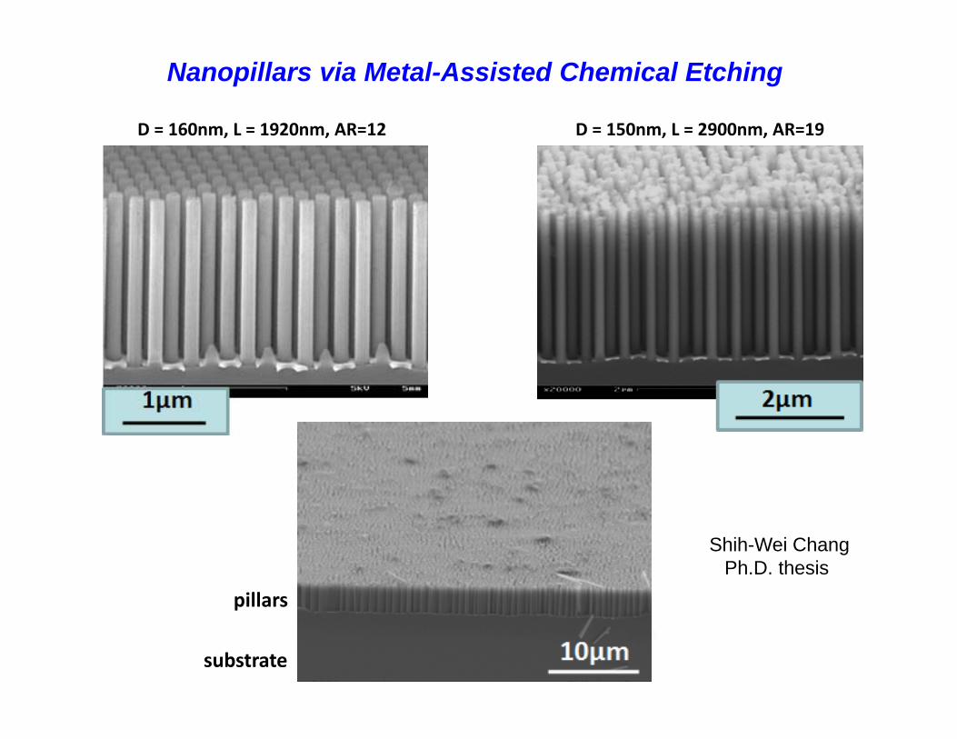
10µm
D = 160nm, L = 1920nm, AR=12 D = 150nm, L = 2900nm, AR=19
pillars
substrate
Nanopillars via Metal-Assisted Chemical Etching
Shih-Wei ChangPh.D. thesis

Metal-Assisted Chemical Etching: Mechanism(s)
Hexafluorosilicic acid
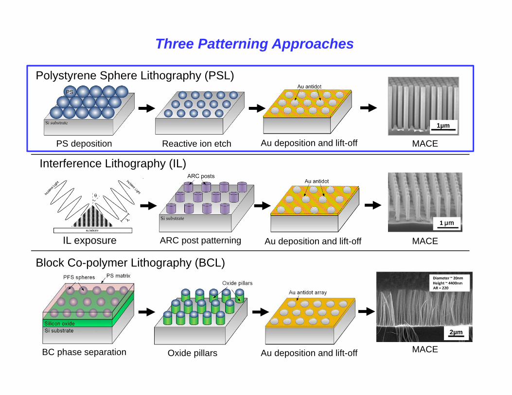
Block Co-polymer Lithography (BCL)
Interference Lithography (IL)
MACEIL exposure ARC post patterning Au deposition and lift-off
Polystyrene Sphere Lithography (PSL)
PS deposition Reactive ion etch Au deposition and lift-off MACE
1µm
Au deposition and lift-off MACEBC phase separation Oxide pillars
2µm
Three Patterning Approaches

Polystyrene sphere monolayer
After reactive ion etching After metal deposition and lift‐off
1µm10µm
D = 160nmL = 1920nm(AR=12)
2µmD = 150nmL = 2900nm(AR=19)
1µm1µm 2µm
pillars
substrate
MACE
Nanopillars via Metal Catalyzed Etching
Shih-Wei Chang, Ph.D. thesis (after Z. Huang et al, Adv. Mat.19, p744, 2007)
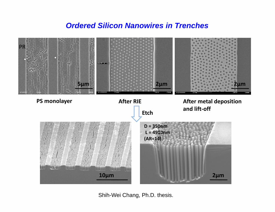
PS monolayer After RIE After metal deposition and lift‐off
PR
5µm
Etch
10µm 2µm
D = 350nmL = 4910nm(AR=14)
2µm2µm
Ordered Silicon Nanowires in Trenches
Shih-Wei Chang, Ph.D. thesis.

Block Co-polymer Lithography (BCL)
Interference Lithography (IL)
MACEIL exposure ARC post patterning Au deposition and lift-off
Polystyrene Sphere Lithography (PSL)
PS deposition Reactive ion etch Au deposition and lift-off MACE
1µm
Au deposition and lift-off MACEBC phase separation Oxide pillars
2µm
Three Patterning Approaches
9

Two exposures, one rotated with respect to the other, creates a 2D array of doubly exposed spots
Using Interference Lithography to Make 2D Arrays
over ~1cm2
sin2P
• Coherent light interferes with itself to form standing wave
• Two orthogonal exposures

Pre-Patterning of Silicon/SiO2 Surface Using Interference Lithography
Interference lithography pattern transferred from a tri-layer mask to Silicon by anisotropic wet etching with KOH
sin2P
• Coherent light interferes with itself to form standing wave
• 1 exposure gives grating
• 2 at an angle give array of posts or holes

Using Interference Lithography to Anti-Dot Arrays
Use two IL exposures to pattern oxide dot array
Deposit and dissolve oxide to ‘lift-off’ metal
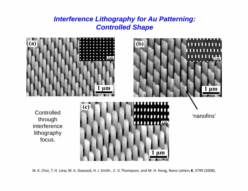
Interference Lithography for Au Patterning:Controlled Shape
Controlled through
interference lithography
focus.
‘nanofins’
W. K. Choi, T. H. Liew, M. K. Dawood, H. I. Smith , C. V. Thompson, and M. H. Hong, Nano Letters 8, 3799 (2008).
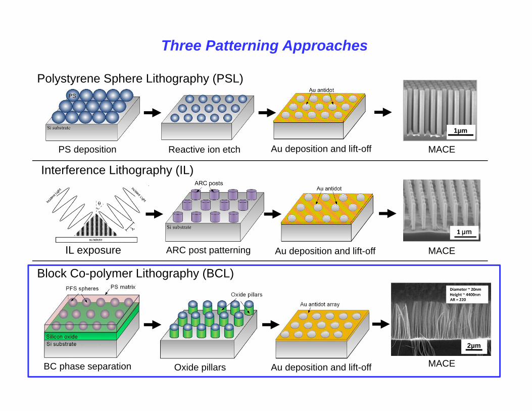
Block Co-polymer Lithography (BCL)
Interference Lithography (IL)
MACEIL exposure ARC post patterning Au deposition and lift-off
Polystyrene Sphere Lithography (PSL)
PS deposition Reactive ion etch Au deposition and lift-off MACE
1µm
Au deposition and lift-off MACEBC phase separation Oxide pillars
2µm
Three Patterning Approaches

PS(Polystyrene)
PFS(Polyferrocenyldimethylsilane)
Self-Assembly of Copolymers
Prof. C.A. Ross
Di-block Copolymer
Spin-on in solvent
Anneal
Phase Separation
substrate substrate

- Locally close-packed structures.- No long-range order.
Flat substrate In trenches
- Long range order- Sub-lithographic length scales
J.Y. Cheng, A.M. Mayes, and C.A. Ross, Nature Materials 3, 823 (2004).
Phase Separation to Form Ordered Structures
diameter ~18-35 nmspacing ~ 29-50 nm
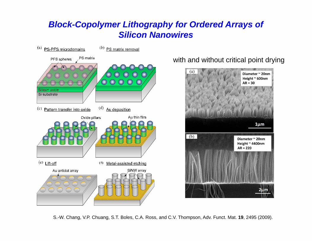
Block-Copolymer Lithography for Ordered Arrays of Silicon Nanowires
with and without critical point drying
S.-W. Chang, V.P. Chuang, S.T. Boles, C.A. Ross, and C.V. Thompson, Adv. Funct. Mat. 19, 2495 (2009).

Konrad Rykaczewski et al, Nano Lett. 2011, 11, 2369–2374
O.J. Hildreth et al , ACS Nano 6, 2012
C.Q. Lai and W.K. Choi, Phys. Chem. Chem. Phys.16, 13402, 2014
Other Structures Made with Silicon MACE

Many Applications of MACE-fabricated Silicon Nanowire Arrays Have Been Investigated
1) Solar cells: with high junction area associated with radially junctions and light trapping
2) Sensors: high surface to volume ratios for high sensitivity3) Thermoelectric devices: phonon scattering at cross-
sectional dimensions (reduced thermal conductivity), with minimal effect on electrical scattering (still high electrical conductivity).
4) Battery electrodes: high charge capacity with increased stress tolerance; high charge/discharge rates due to high surface-to volume ratios.
5) High-value integrated capacitors for power management: associated with high surface-to-volume ratios.
Probably others....
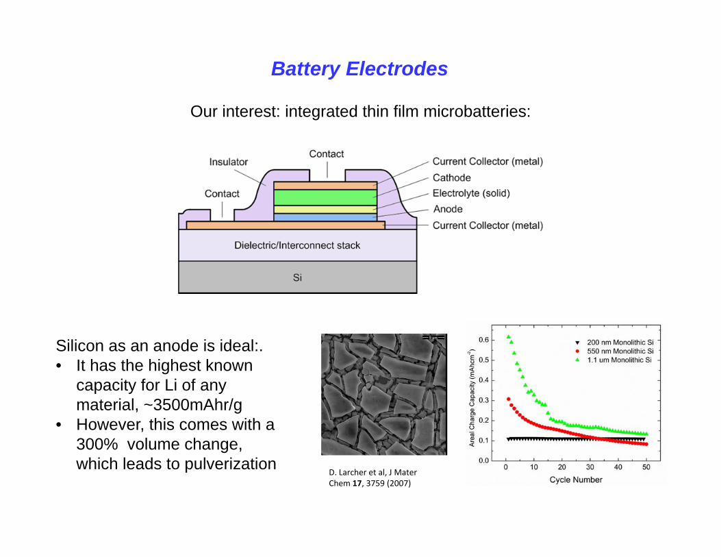
Battery Electrodes
Our interest: integrated thin film microbatteries:
Silicon as an anode is ideal:.• It has the highest known
capacity for Li of any material, ~3500mAhr/g
• However, this comes with a 300% volume change, which leads to pulverization
D. Larcher et al, J Mater Chem 17, 3759 (2007)

• Wires can expand in-plane. Less pulverization. Higher cyclability at higher areal capacites.
• Higher surface-to-volume ratio: higher charge-discharge rate capacity
vs.
(half cells )
R.S. Omampuliyur, M. Bhuiyan, Z Han, Z. Jing, L. Li, E.A. Fitzgerald, C.V. Thompson, W.K. Choi, J. Nanosci. Nanotechnol. 15, 4926 (2015).
Battery Electrodes
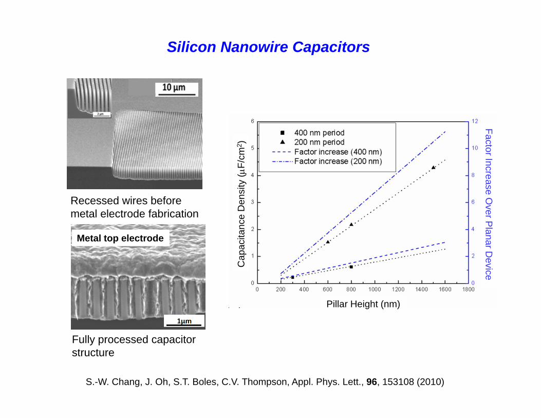
Silicon Nanowire Capacitors
S.-W. Chang, J. Oh, S.T. Boles, C.V. Thompson, Appl. Phys. Lett., 96, 153108 (2010)
Recessed wires before metal electrode fabrication
Fully processed capacitor structure
Metal top electrodeC
apac
itanc
e D
ensi
ty (
F/cm
2 )
Pillar Height (nm)
Factor Increase Over P
lanar Device

Pt MACE with Au etchant Optimized Pt etchant
Nanowires from films instead of wafers
Amorphous wires with single-crystal etchant
Amorphous wires with optimized etchant
Other Metals and Other Etch Chemistries
These results highlight a key issue in MACE: control of pororsity

Metal-Assisted Chemical Etching: Mechanism(s)
Alternative formulation:
Cathode:
Anode:
Overall:
If the ratio of [H2O2] to [HF] is high, the reduction reaction will outpace the oxidation reaction and ‘excess holes’ and H2 will be produced at the metal/Si.

Overall reaction:
Production of Excess Holes
121
HF2O2H ‘excess’ holes are generated
Excess holes can diffuse away from the metal/silicon interface and cause etching
P. Lianto, S. Yu, J. Wu, C.V. Thompson and W.K. Choi, Nanoscale 4, 732-7539 (2012).
h+ injected
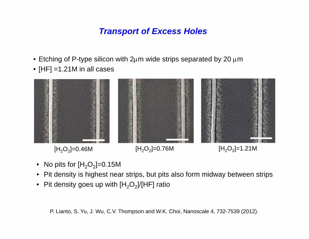
• Etching of P-type silicon with 2m wide strips separated by 20 m• [HF] =1.21M in all cases
• No pits for [H2O2]=0.15M• Pit density is highest near strips, but pits also form midway between strips• Pit density goes up with [H2O2]/[HF] ratio
[H2O2]=0.46M [H2O2]=0.76M [H2O2]=1.21M
Transport of Excess Holes
P. Lianto, S. Yu, J. Wu, C.V. Thompson and W.K. Choi, Nanoscale 4, 732-7539 (2012).

• Etching of P-type silicon with 2m wide strips separated by 20 m• [HF] =1.21M in all cases
[H2O2]=0.46M [H2O2]=0.76M [H2O2]=1.21M
Transport of Excess Holes

strip spacings of 2, 9, 13, 17, and 20 m,
[HF] and [H2O2] fixed at 1.73 and
1.21 M
Transport of Excess Holes and Etch Stability
• Lines that are closely spaced have reduced stability
P. Lianto, S. Yu, J. Wu, C.V. Thompson and W.K. Choi, Nanoscale 4, 732-7539 (2012).

Transport of Excess Holes and Etch Stability
Pit density measured midway between strips
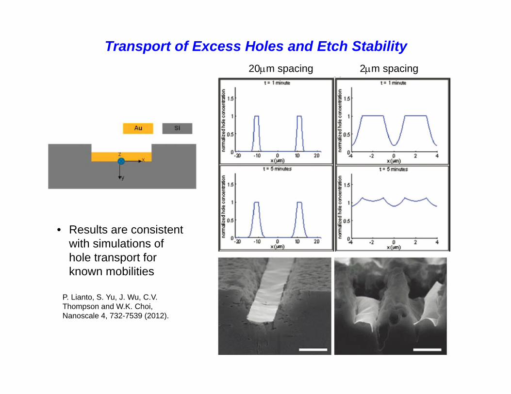
• Results are consistent with simulations of hole transport for known mobilities
20m spacing 2m spacing
Transport of Excess Holes and Etch Stability
P. Lianto, S. Yu, J. Wu, C.V. Thompson and W.K. Choi, Nanoscale 4, 732-7539 (2012).

U = 0V U = 10V U = 100V[HF]=1.73M and [H2O2]=1.21M
Field-modified MACE
P. Lianto, S. Yu, J. Wu, C.V. Thompson and W.K. Choi, Nanoscale 4, 7532 (2012)

[HF] = 1.73 M and [H2O2] = 1.21 M,
unetched U = 0V
U = 10V U =100V
Field-modified MACE
Pits form on the unpolished back-side of the wafer
P. Lianto, S. Yu, J. Wu, C.V. Thompson and W.K. Choi,, Nanoscale 4, 7532 (2012)

MACE EMACE
Li et al* subsequently carried out further studies and extensively confirmed the benefit of an external field in controlling pit formation and etch stability. They also named the process EMACE (Electric-field-attenuated MACE).
Field-modified MACE
*L. Li, X. Zhao, and C.-P. Wong, Appl. Mat. Int. 6, 16782 (2014).

1) P. Lianto et al, Nanoscale 4, 7532 (2012).2) L. Li et al, Appl. Mat. Int. 6, 16782 (2014).3) Z.P. Huang et al, Nanotech. 21, 465301(2010). 4) C.Q. Lai et al, Nanoscale 7, 11123 (2015).
MAAE4
Metal Assisted Anodic Etching

Anodic Etching of Silicon
• Widely studied and used to make layers of porous silicon:• Purely electrochemical in nature• Electrochemical etching of Si in HF (no H2O2 or other oxidant)

Metal Assisted Anodic Etching (MAAE)
Silicon sample withperforated Au film on top
Anodic contact to silicon
Back-side contact to Cu through an Al film for ohmic contact to n-type silicon or Au for ohmic contact to p-type silicon.
C.Q. Lai, W. Zheng, W.K. Choi, and C.V. Thompson, Nanoscale 7, 11123 (2015).

Metal Assisted Anodic Etching (MAAE)
Anodic contact to gold
C.Q. Lai, W. Zheng, W.K. Choi, and C.V. Thompson, Nanoscale 7, 11123 (2015).

‘MACE-Like’
‘Anodic-Etching-
Like’
P-type N-type
MAAE Experiments

•Van der Waal forces hold the metal in contact.
•Metal and silicon always in contact somewhere along the interface.
Holes generated at the M/HF interface cross the M/Si interface. Reaction occurs by hole transport across the HF/Si interface.
Follow the Holes

Injection of Holes from Gold
• Hole transport occurs across two interfaces.• Schottky barriers form in both in both cases.• Barrier heights N and N for N-type silicon, similarly for P-type
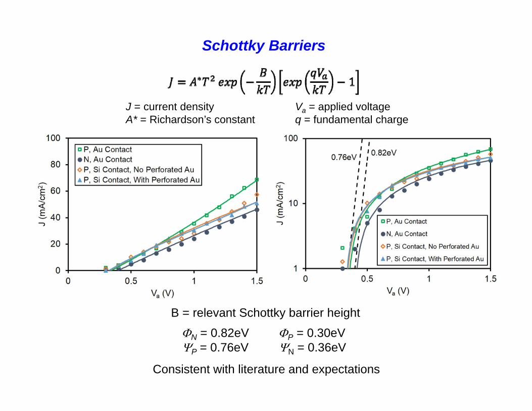
J = current densityA* = Richardson’s constant
Va = applied voltageq = fundamental charge
B = relevant Schottky barrier height
N = 0.82eV P = 0.30eVP = 0.76eV N = 0.36eV
Consistent with literature and expectations
Schottky Barriers

‘MACE-Like’
‘Anodic-Etching-
Like’
P-type N-type
MAAE Experiments
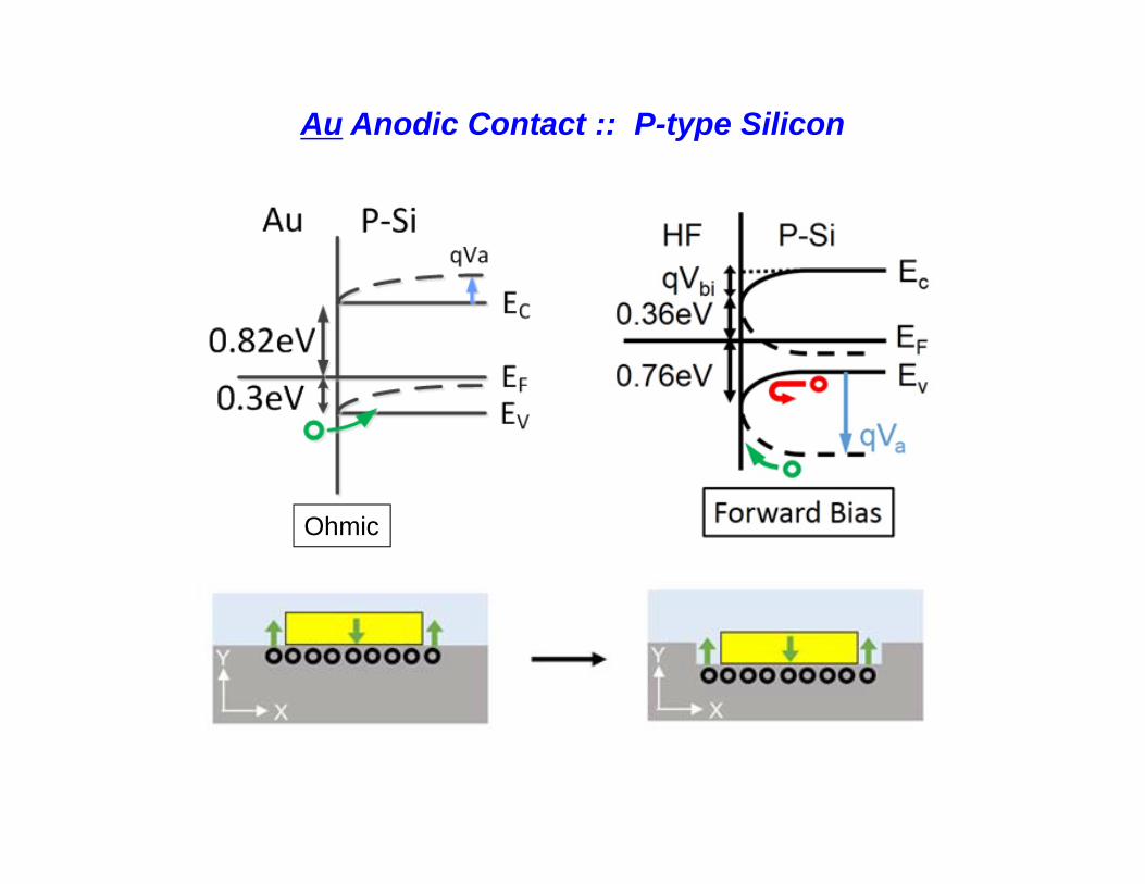
Au Anodic Contact :: P-type Silicon
Ohmic
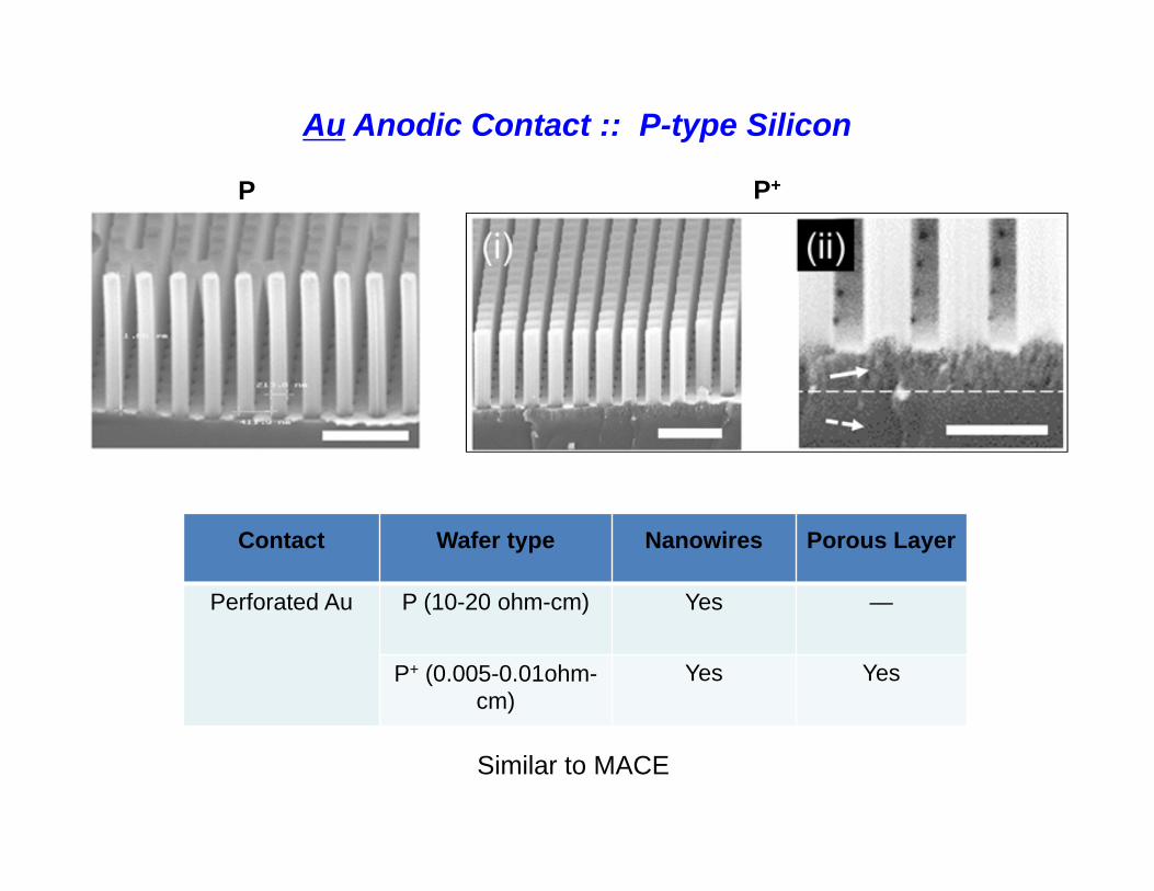
Contact Wafer type Nanowires Porous Layer
Perforated Au P (10-20 ohm-cm) Yes —
P+ (0.005-0.01ohm-cm)
Yes Yes
P P+
Similar to MACE
Au Anodic Contact :: P-type Silicon
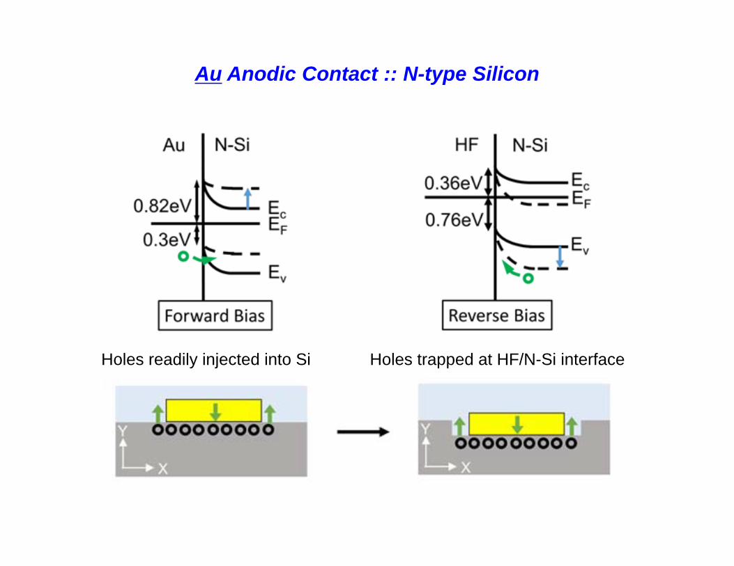
Au Anodic Contact :: N-type Silicon
Holes trapped at HF/N-Si interfaceHoles readily injected into Si

Contact Wafer type Nanowires Porous Layer
Perforated Au N (10-30ohm-cm) Yes —
N+ (<0.005ohm -
cm)
Yes Yes
Au Anodic Contact :: N-type SiliconN N+
Porous wires, porous layer under wiresSolid wires
Similar to MACE
Va < Vbi
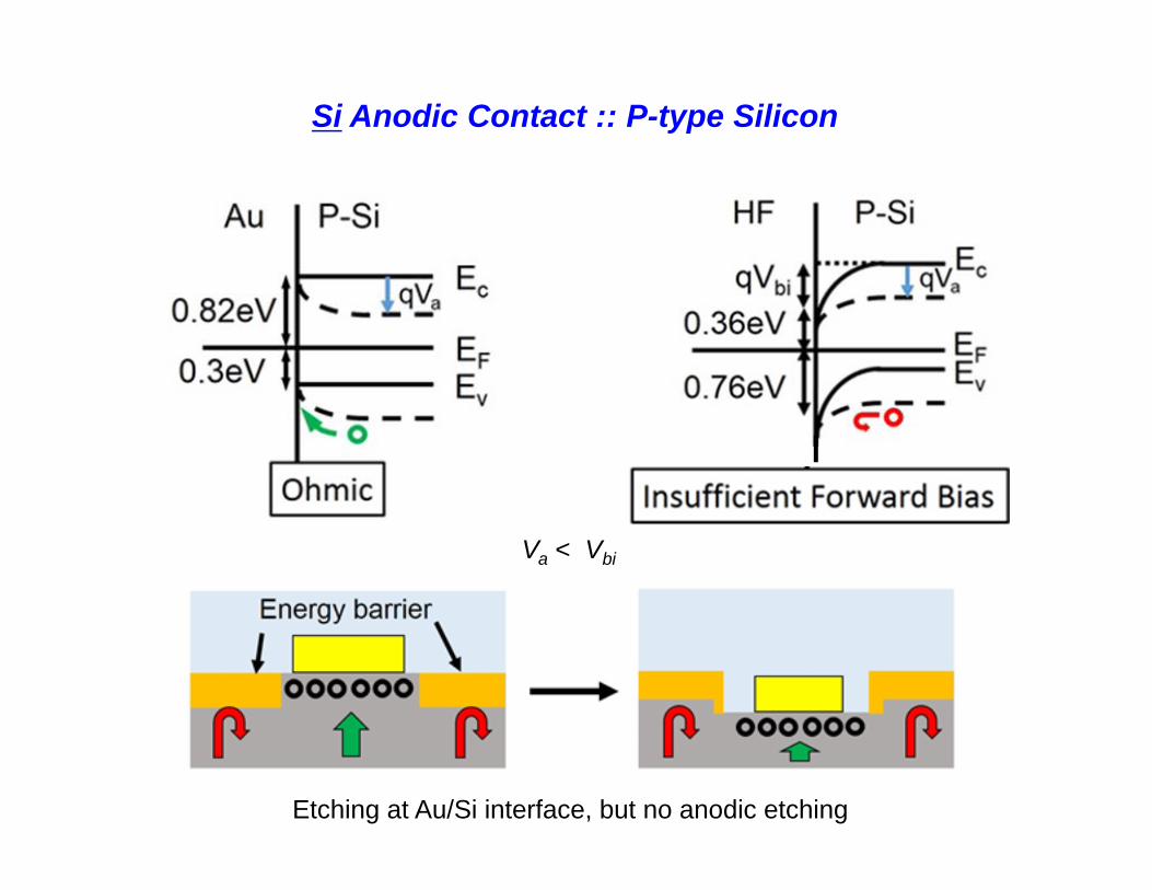
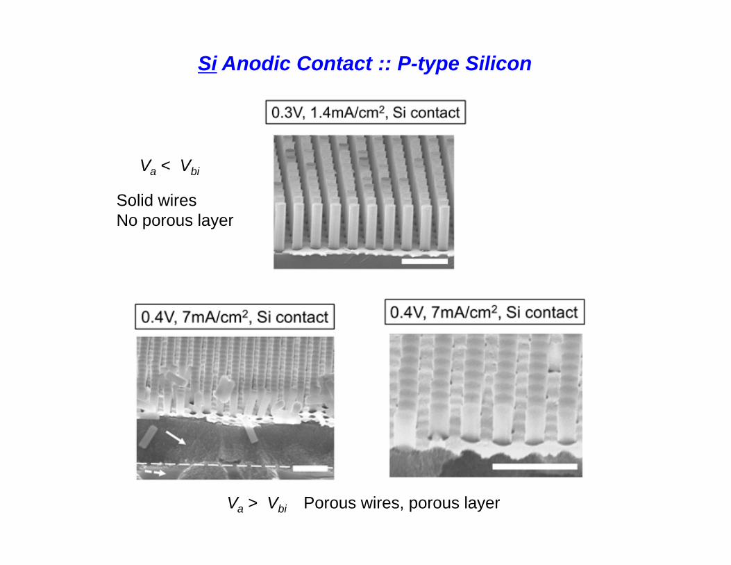
Si Anodic Contact :: P-type Silicon
Etching at Au/Si interface, but no anodic etching
Si Anodic Contact :: P-type Silicon
Va < Vbi
Solid wiresNo porous layer
Va > Vbi Porous wires, porous layer
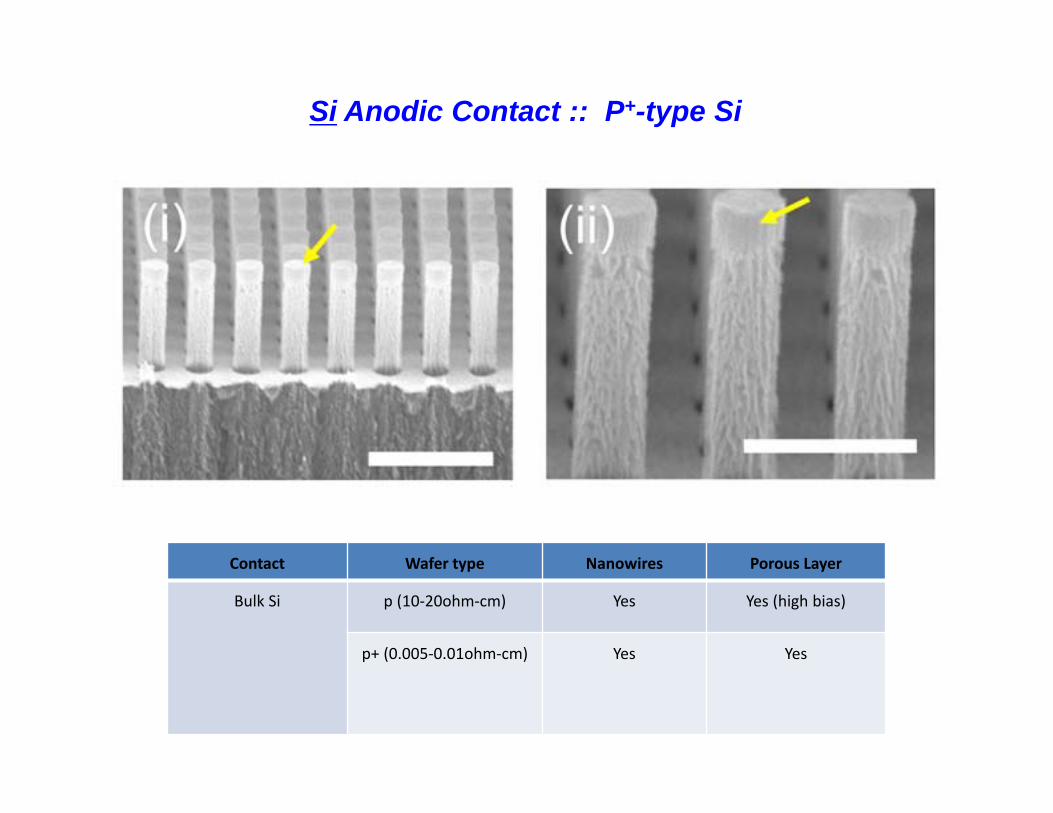
Contact Wafer type Nanowires Porous Layer
Bulk Si p (10‐20ohm‐cm) Yes Yes (high bias)
p+ (0.005‐0.01ohm‐cm) Yes Yes
Si Anodic Contact :: P+-type Si
Si Anodic Contact :: N-type Si
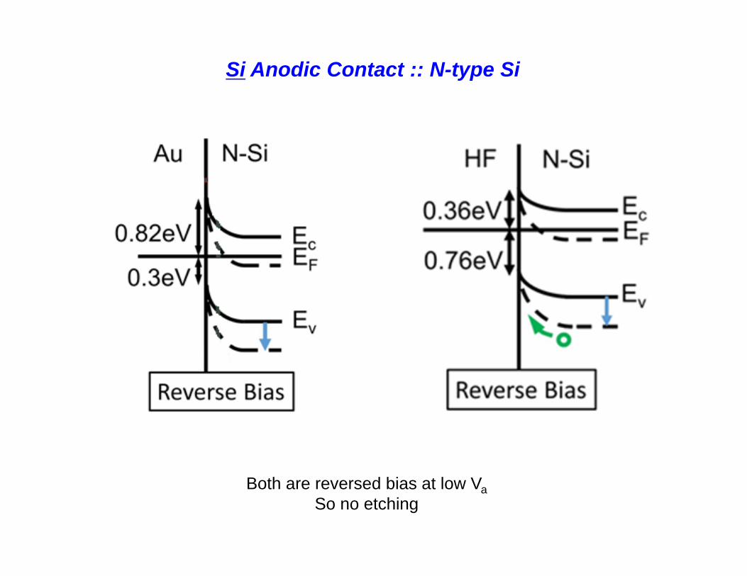
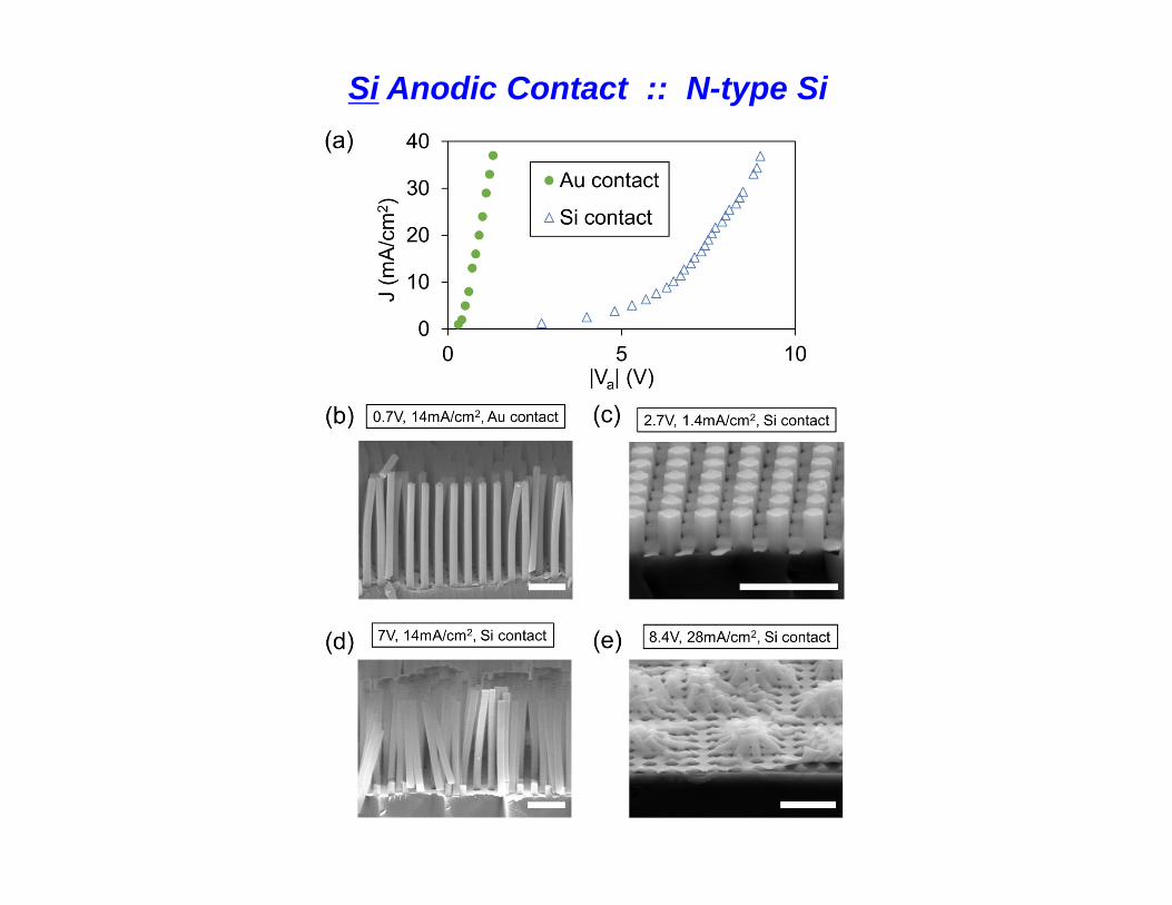
Si Anodic Contact :: N-type Si
Both are reversed bias at low VaSo no etching

Si Anodic Contact :: N-type Si
At high bias breakdown due to impact ionization occurs at edges of Au.Generated holes are confined to N-Si interfaces.
Breakdown

Contact Wafer type Nanowires Porous Layer
Bulk‐Si n (10-30ohm-cm) Yes
(porous)
—
Si Anodic Contact :: N-type Si

Contact Wafer type Nanowires Porous Layer
Bulk‐Si n (10-30ohm-cm) Yes —
n+ (<0.005ohm-cm) — Yes
Si Anodic Contact :: N+-type Si
Similar to metal-free anodic etching

Si Anodic Contact :: N+-type Si
Breakdown at HF/N+-Si interface
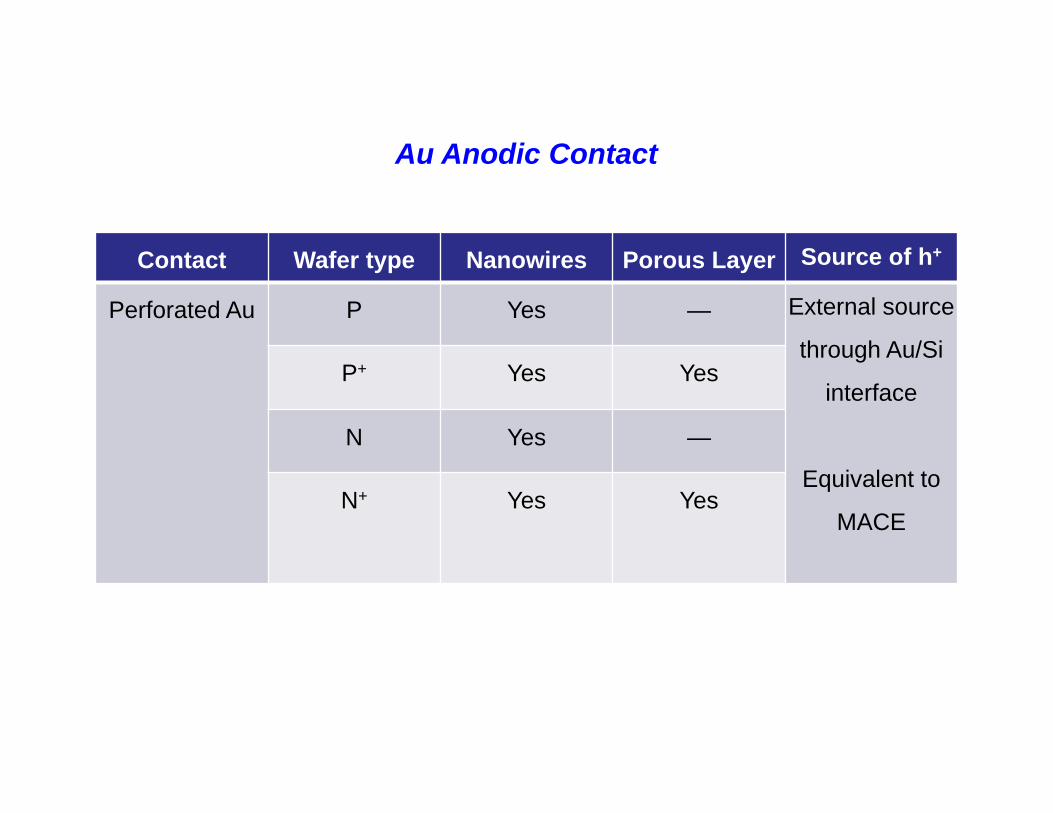
Contact Wafer type Nanowires Porous Layer Source of h+
Perforated Au P Yes — External source
through Au/Si
interface
Equivalent to
MACE
P+ Yes Yes
N Yes —
N+ Yes Yes
Au Anodic Contact

Contact Wafer type Nanowires Porous Layer Source of h+
Bulk Si P Yes Yes
(high bias) External source through both Au/Si and
etchant/Si interfaces
Equivalent to MACE + Anodic Etching
P+ Yes Yes
N Yes — Breakdown at Au/Si interface
N+ — Yes Breakdown at etchant/Si interface
Si Anodic Contact
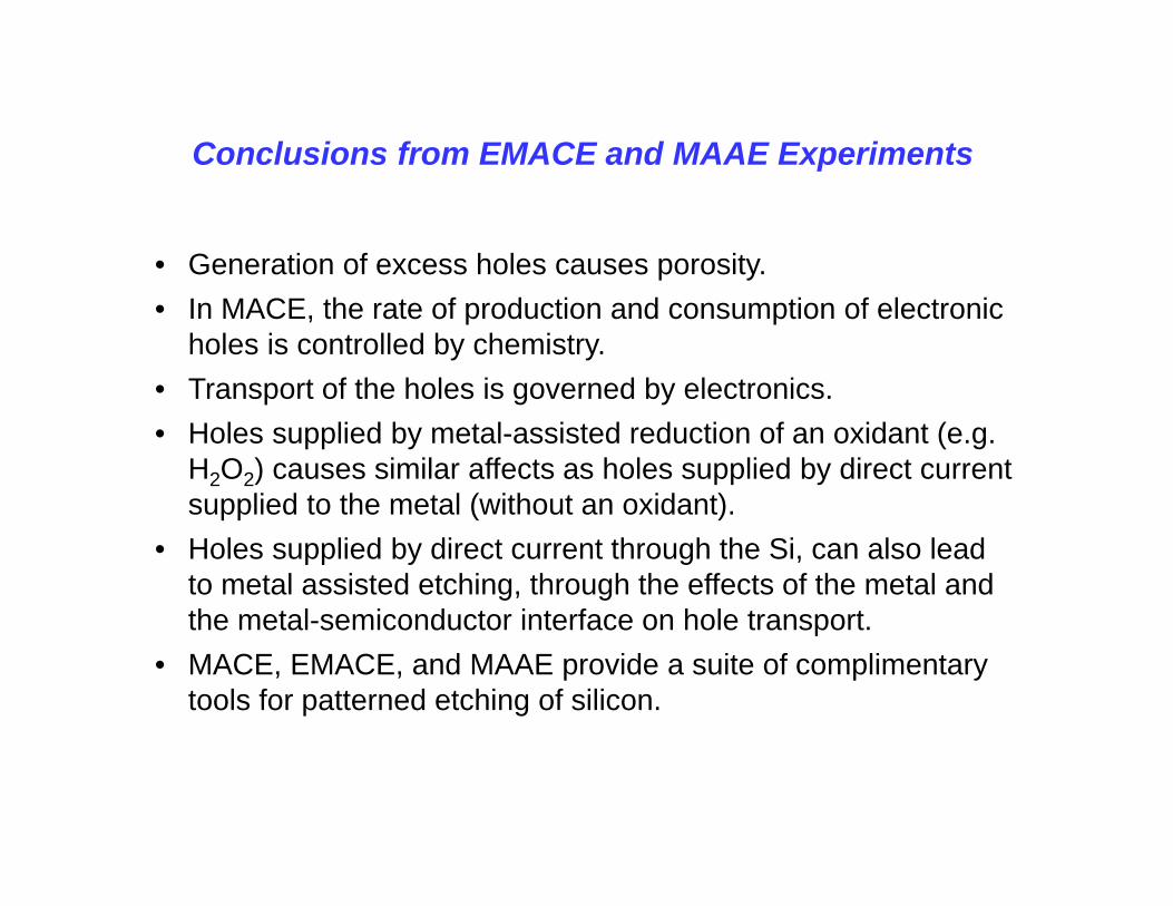
Conclusions from EMACE and MAAE Experiments
• Generation of excess holes causes porosity.• In MACE, the rate of production and consumption of electronic
holes is controlled by chemistry.• Transport of the holes is governed by electronics.• Holes supplied by metal-assisted reduction of an oxidant (e.g.
H2O2) causes similar affects as holes supplied by direct current supplied to the metal (without an oxidant).
• Holes supplied by direct current through the Si, can also lead to metal assisted etching, through the effects of the metal and the metal-semiconductor interface on hole transport.
• MACE, EMACE, and MAAE provide a suite of complimentary tools for patterned etching of silicon.

Overall Summary
• MACE and related processes provide simple, low-cost , and versatile methods for producing arrays of silicon nanostructures.
• Improved mechanistic understandings are leading to better control of porosity.
• Challenges remain to extended this technique to a wider range of semiconductors. Basic studies should help overcome these challenges.