Mems technologies and analysis of merits and demerits
19
MEMS TECHNOLOGIES AND ANALYSIS OF MERITS AND DEMERITS THEREOF - BIPRASISH RAY (2015H123031G)
-
Upload
biprasish-ray -
Category
Engineering
-
view
1.136 -
download
0
Transcript of Mems technologies and analysis of merits and demerits

MEMS TECHNOLOGIES AND
ANALYSIS OF MERITS AND
DEMERITS THEREOF
- BIPRASISH RAY
(2015H123031G)

CONTENTS
INTRODUCTION
FABRICATION PROCESS
FABRICATION TECHNIQUE
APPLICATIONS
ADVANTAGES AND DISADVANTAGES
CONCLUSION
FUTURE SCOPE

WHAT IS MEMS?
MEMS stands for MICROELECTROMECHANICAL SYSTEMS

MMicro: Small size, micro fabricated structures.
E Electro: Electrical signal control.
MMechanical: Mechanical functionality.
S Systems: Structures, Devices, System Controls.
MEMS devices generally range in size from 20
micrometers to a millimeter

COMPONENTS OF MEMS DEVICE MICROACTUATORS AND
MICROSENSORS FORM THE
MOST IMPORTANT
COMPONENTS OF A MEMS
DEVICE.
N
S
EW 2 Axis Magnetic
Sensor2 Axis
AccelerometerLight Intensity
SensorHumidity Sensor
Pressure Sensor
Temperature
Sensor
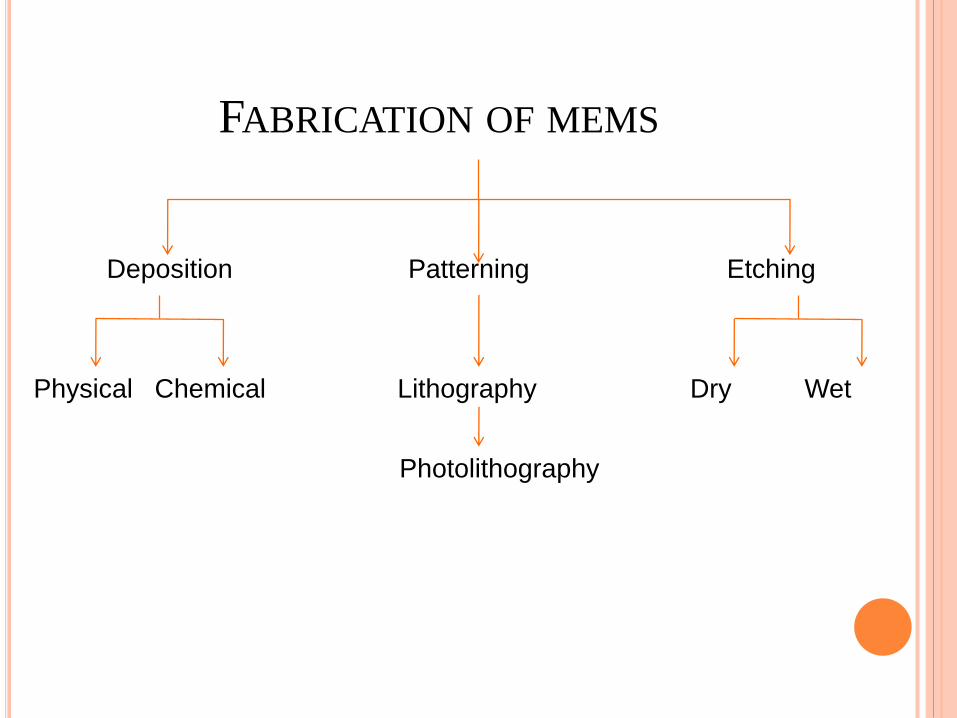
FABRICATION OF MEMS
Deposition Patterning Etching
Physical Chemical Lithography Dry Wet
Photolithography


PACKAGING:
o Metal can package
o Plastic package
o Ceramic package

FABRICATION TECHNIQUE
The fabrication technique of MEMS devices is called
Micromachining or Microfabrication.
The fabrication of MEMS evolved from the process
technology in semiconductor device fabrication.
Two basic methods of MEMS integration are:
Surface Micromachining
Bulk Micromachining

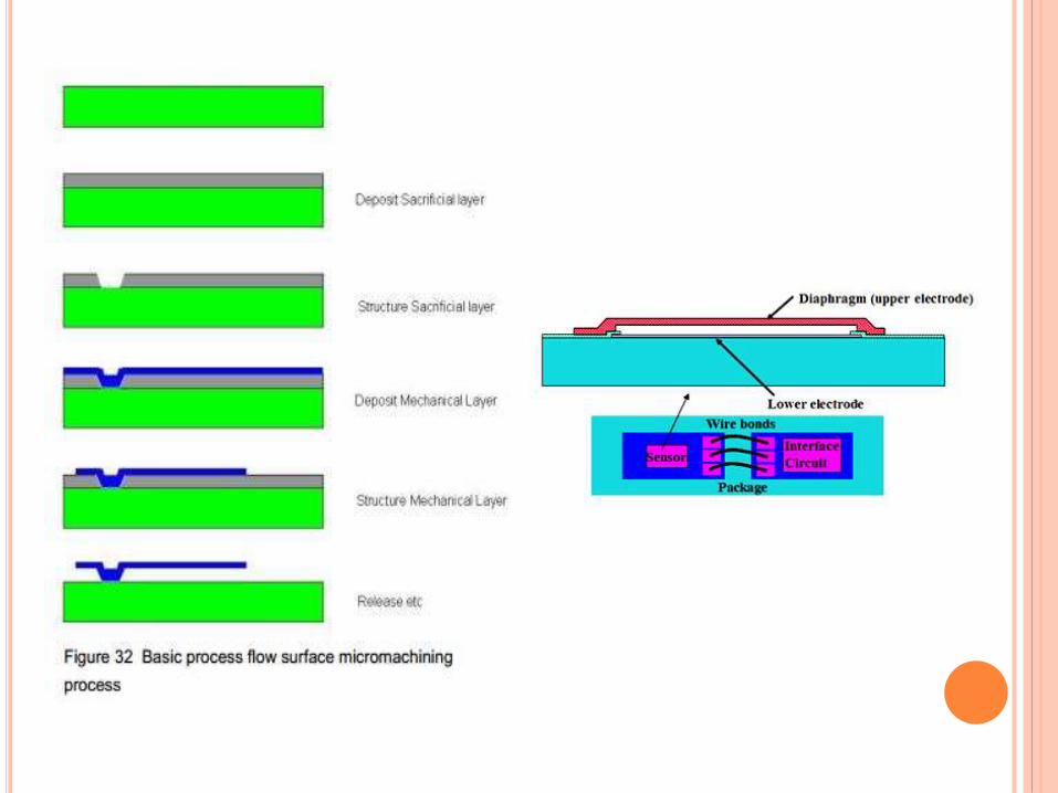
SURFACE MICROMACHINING
In surface micromachining, the MEMS sensors are formed on
top of the wafer using deposited thin film materials. The
surface micromachined sensors use the capacitive
transduction method to convert the input mechanical signal
to the equivalent electrical signal.
One of the most important processing steps that is required of
dynamic MEMS devices is the selective removal of an
underlying film, referred to as a sacrificial layer, without
attacking an overlaying film, referred to as the structural
layer, used to create the mechanical parts.
Enables low cost accelerometers.

BULK MICROMACHINING
Bulk micromachining is an extension of IC technology for the
fabrication of 3D structures.
The whole thickness of a silicon wafer is used for building the
micro-mechanical structures.
The transduction mechanism that has been widely used is
the piezoresistive effect. In piezoresistive materials, a change
in the stress causes a strain and a corresponding change in the
resistance.
Enables high performance microactuators and microsensors.


APPLICATIONS OF MEMS

APPLICATIONS OF MEMS

ADVANTAGES AND DISADVANTAGES
Minimize energy and
materials.
Improved reproducibility.
Improved sensitivity,
accuracy and reliability
Low cost and low power.
Easier to alter the parts of
a device as compared to
its macro counterpart.
Farm establishment
requires huge
investments.
Polysilicon is a brittle
material.
Design includes very
much complex
procedures.
CONCLUSION
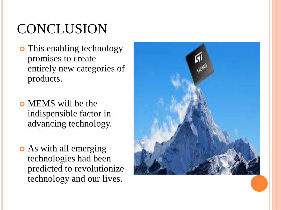
This enabling technology promises to create entirely new categories of products.
MEMS will be the indispensible factor in advancing technology.
As with all emerging technologies had been predicted to revolutionize technology and our lives.

FUTURE SCOPE
In order to avoid the need for a multitude of wires, such
sensors must be self sustaining and able to communicate
wirelessly.
As a result, not only more sensors are needed, but also small
energy generating modules and wireless transmission
components. Clearly, the increased numbers of devices will
drive size reduction which in turn will enable higher levels of
integration.
This prediction combined with the foregoing discussion on the
advantages of MEMS over macro devices lead us to predict
that MEMS will soon be integrated into our everyday life just
as the computers have been.