MEMS audio sensor omnidirectional digital microphone · MEMS audio sensor omnidirectional digital...
16
June 2016 DocID029435 Rev 1 1/16 This is information on a product in full production. www.st.com MP45DT02-M MEMS audio sensor omnidirectional digital microphone Datasheet - production data Features • Single supply voltage • Low power consumption • 120 dBSPL acoustic overload point • Omnidirectional sensitivity • PDM single-bit output with option for stereo configuration • HLGA metal package (SMD-compliant) • ECOPACK ® , RoHS, and “Green” compliant Applications • Mobile terminals • Laptop and notebook computers • Portable media players • VoIP • Speech recognition • A/V eLearning devices • Gaming and virtual reality input devices • Digital still and video cameras • Antitheft systems Description The MP45DT02-M is a compact, low-power, top- port, omnidirectional, digital MEMS microphone. The MP45DT02-M is built with a sensing element and an IC interface with stereo capability. The sensing element, capable of detecting acoustic waves, is manufactured using a specialized silicon micromachining process to produce audio sensors. The IC interface is manufactured using a CMOS process that allows designing a dedicated circuit able to provide a digital signal externally in PDM format. The MP45DT02-M has an acoustic overload point of 120 dBSPL with a best on the market 61 dB signal-to-noise ratio and -26 dB sensitivity. The MP45DT02-M is available in an SMD- compliant metal package and is guaranteed to operate over an extended temperature range from -30 °C to +85 °C. The MP45DT02-M’s digital output and package size (1.25 mm thick) make this device the best solution for laptop and portable computing applications. Table 1: Device summary Order code Temp. range [°C] Package Packing MP45DT02TR-M -30 to +85 HLGA 4.72 x 3.76 6LD Tape and reel
Transcript of MEMS audio sensor omnidirectional digital microphone · MEMS audio sensor omnidirectional digital...

June 2016 DocID029435 Rev 1 1/16
This is information on a product in full production. www.st.com
MP45DT02-M
MEMS audio sensor omnidirectional digital microphone
Datasheet - production data
Features • Single supply voltage • Low power consumption • 120 dBSPL acoustic overload point • Omnidirectional sensitivity • PDM single-bit output with option for stereo
configuration • HLGA metal package (SMD-compliant) • ECOPACK®, RoHS, and “Green” compliant
Applications • Mobile terminals • Laptop and notebook computers • Portable media players • VoIP • Speech recognition • A/V eLearning devices • Gaming and virtual reality input devices • Digital still and video cameras • Antitheft systems
Description The MP45DT02-M is a compact, low-power, top-port, omnidirectional, digital MEMS microphone. The MP45DT02-M is built with a sensing element and an IC interface with stereo capability.
The sensing element, capable of detecting acoustic waves, is manufactured using a specialized silicon micromachining process to produce audio sensors.
The IC interface is manufactured using a CMOS process that allows designing a dedicated circuit able to provide a digital signal externally in PDM format.
The MP45DT02-M has an acoustic overload point of 120 dBSPL with a best on the market 61 dB signal-to-noise ratio and -26 dB sensitivity.
The MP45DT02-M is available in an SMD-compliant metal package and is guaranteed to operate over an extended temperature range from -30 °C to +85 °C.
The MP45DT02-M’s digital output and package size (1.25 mm thick) make this device the best solution for laptop and portable computing applications.
Table 1: Device summary Order code Temp. range [°C] Package Packing
MP45DT02TR-M -30 to +85 HLGA
4.72 x 3.76 6LD Tape and reel
Contents MP45DT02-M
2/16 DocID029435 Rev 1
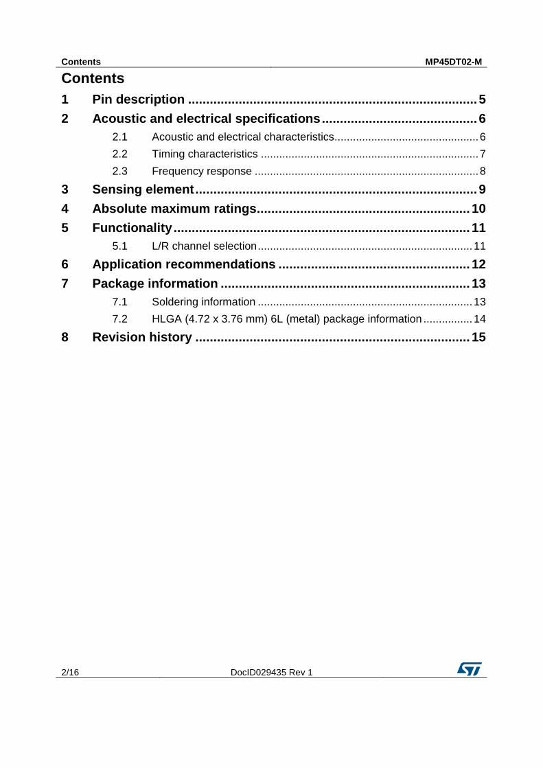
Contents 1 Pin description ................................................................................ 5
2 Acoustic and electrical specifications ........................................... 6
2.1 Acoustic and electrical characteristics ............................................... 6
2.2 Timing characteristics ....................................................................... 7
2.3 Frequency response ......................................................................... 8
3 Sensing element .............................................................................. 9
4 Absolute maximum ratings ........................................................... 10
5 Functionality .................................................................................. 11
5.1 L/R channel selection ...................................................................... 11
6 Application recommendations ..................................................... 12
7 Package information ..................................................................... 13
7.1 Soldering information ...................................................................... 13
7.2 HLGA (4.72 x 3.76 mm) 6L (metal) package information ................ 14
8 Revision history ............................................................................ 15

MP45DT02-M List of tables
DocID029435 Rev 1 3/16
List of tables Table 1: Device summary ........................................................................................................................... 1 Table 2: Pin description .............................................................................................................................. 5 Table 3: Acoustic and electrical characteristics .......................................................................................... 6 Table 4: Distortion specifications ................................................................................................................ 6 Table 5: Timing characteristics ................................................................................................................... 7 Table 6: Absolute maximum ratings ......................................................................................................... 10 Table 7: L/R channel selection ................................................................................................................. 11 Table 8: Recommended soldering profile limits ........................................................................................ 13 Table 9: Document revision history .......................................................................................................... 15

List of figures MP45DT02-M
4/16 DocID029435 Rev 1
List of figures Figure 1: Pin connections ........................................................................................................................... 5 Figure 2: Timing waveforms ....................................................................................................................... 7 Figure 3: Typical frequency response normalized at 1 kHz........................................................................ 8 Figure 4: MP45DT02-M electrical connections ......................................................................................... 12 Figure 5: MP45DT02-M electrical connections for stereo configuration ................................................... 12 Figure 6: Recommended soldering profile limits ...................................................................................... 13 Figure 7: HLGA (4.72 x 3.76 mm) 6-lead package outline and mechanical data ..................................... 14

MP45DT02-M Pin description
DocID029435 Rev 1 5/16
1 Pin description Figure 1: Pin connections
Table 2: Pin description
Pin n°
Pin name Function
1 GND 0 V supply
2 LR Left/right channel selection; MIC1 LR is connected to GND or Vdd and MIC2 LR is connected to Vdd or GND (see Figure 5: "MP45DT02-M electrical connections for stereo configuration"
3 GND 0 V supply
4 CLK Synchronization input clock
5 DOUT Left/right PDM data output
6 Vdd Power supply
)WEIVMOTTOB(
DOUT
CLK
Vdd
LR
GND
GND
1
34
5
6
5
4
1
2
3

Acoustic and electrical specifications MP45DT02-M
6/16 DocID029435 Rev 1
2 Acoustic and electrical specifications
2.1 Acoustic and electrical characteristics The values listed in the table below are specified for Vdd = 1.8 V, Clock = 2.4 MHz, T = 25 °C, unless otherwise noted.
Table 3: Acoustic and electrical characteristics Symbol Parameter Test condition Min. Typ.(1) Max. Unit
Vdd Supply voltage
1.64 1.8 3.6 V
Idd Current consumption in normal mode No load on data line
0.65
mA
IddPdn Current consumption in power-down mode (2)
20
µA
Scc Short-circuit current
1
10 mA
AOP Acoustic overload point
120
dBSPL
So Sensitivity
-29 -26 -23 dBFS
SNR Signal-to-noise ratio A-weighted @1 kHz, 1 Pa
61
dB
PSR Power supply rejection Guaranteed by design (3)
-70
dBFS
Clock Input clock frequency (4)
1 2.4 3.25 MHz
TWK Wake-up time (5) Guaranteed by design
10 ms
Top Operating temperature range
-30
+85 °C
VIOL Low level logic input/output voltage Iout = 1 mA -0.3
0.35xVdd V
VIOH High level logic input/output voltage Iout = 1 mA 0.65xVdd
Vdd+0.3 V
Notes: (1)Typical specifications are not guaranteed. (2)Input clock in static mode. (3)Test signal: 217 Hz square wave, 100 mVpp on Vdd pin. (4)Duty cycle: min = 40% max = 60%. (5)Time from the first clock edge to valid output data.
Table 4: Distortion specifications Parameter Test condition Value
Distortion 100 dBSPL (50 Hz - 4 kHz) < 1% THD + N
Distortion 115 dBSPL (1 kHz) < 5% THD + N

MP45DT02-M Acoustic and electrical specifications
DocID029435 Rev 1 7/16
2.2 Timing characteristics Table 5: Timing characteristics
Parameter Description Min Max Unit
fCLK Clock frequency for normal mode 1 3.25 MHz
fPD Clock frequency for power-down mode
0.23 MHz
TCLK Clock period for normal mode 308 1000 ns
TR,EN Data enabled on DATA line, L/R pin = 1 30 (1)
ns
TR,DIS Data disabled on DATA line, L/R pin = 1
16(1)(2) ns
TL,EN Data enabled on DATA line, L/R pin = 0 30(1)
ns
TL,DIS Data disabled on DATA line, L/R pin = 0
16(1)(2) ns
Notes: (1)From design simulations (2)In order to measure the disable time, a 1 kΩ pull-down resistor must be added to the DOUT pin.
Figure 2: Timing waveforms

Acoustic and electrical specifications MP45DT02-M
8/16 DocID029435 Rev 1
2.3 Frequency response Figure 3: Typical frequency response normalized at 1 kHz

MP45DT02-M Sensing element
DocID029435 Rev 1 9/16
3 Sensing element The sensing element shall mean the acoustic sensor consisting of a conductive movable plate and a fixed plate placed in a tiny silicon chip. This sensor transduces the sound pressure into the changes of coupled capacity between those two plates.
Omron Corporation supplies this element for STMicroelectronics.

Absolute maximum ratings MP45DT02-M
10/16 DocID029435 Rev 1
4 Absolute maximum ratings Stresses above those listed as “absolute maximum ratings” may cause permanent damage to the device. This is a stress rating only and functional operation of the device under these conditions is not implied. Exposure to maximum rating conditions for extended periods may affect device reliability.
Table 6: Absolute maximum ratings Symbol Ratings Maximum value Unit
Vdd Supply voltage -0.3 to 6 V
Vin Input voltage on any control pin -0.3 to Vdd +0.3 V
TSTG Storage temperature range -40 to +125 °C
ESD Electrostatic discharge protection 2 (HBM) kV

MP45DT02-M Functionality
DocID029435 Rev 1 11/16
5 Functionality
5.1 L/R channel selection The L/R digital pad lets the user select the DOUT signal pattern as explained in Table 7: "L/R channel selection". The L/R pin must be connected to Vdd or GND.
Table 7: L/R channel selection L/R CLK low CLK high
GND Data valid High impedence
Vdd High impedence Data valid

Application recommendations MP45DT02-M
12/16 DocID029435 Rev 1
6 Application recommendations Figure 4: MP45DT02-M electrical connections
Figure 5: MP45DT02-M electrical connections for stereo configuration
Power supply decoupling capacitors (100 nF ceramic, 10 µF ceramic) should be placed as near as possible to pin 6 of the device (common design practice).
The L/R pin must be connected to Vdd or GND (refer to Table 7: "L/R channel selection").
Vdd
1
2
3 4
5
6
CLK
Dout
10 µF
100 nF
L/R
TOP
VIEW
CO
DE
C
D out
TOP
VIE
W
CODEC
Vdd
Vdd
10 µ F
100 nF
CLK
MIC 1 MIC 2
Dout
TOPVIEW
1
2
3 4
5
61
2
3 4
5
6

MP45DT02-M Package information
DocID029435 Rev 1 13/16
7 Package information In order to meet environmental requirements, ST offers these devices in different grades of ECOPACK® packages, depending on their level of environmental compliance. ECOPACK® specifications, grade definitions and product status are available at: www.st.com. ECOPACK® is an ST trademark.
7.1 Soldering information The HLGA (4.72 x 3.76 x 1.25) mm package is also compliant with the RoHS and “Green” standards and is qualified for soldering heat resistance according to JEDEC J-STD-020.
Landing pattern and soldering recommendations are available at www.st.com. Figure 6: Recommended soldering profile limits
Table 8: Recommended soldering profile limits
Description Parameter Pb free
Average ramp rate TL to TP 3 °C/sec max
Preheat Minimum temperature Maximum temperature Time (TSMIN to TSMAX)
TSMIN TSMAX
tS
150 °C 200 °C
60 sec to 120 sec
Ramp-up rate TSMAX to TL
Time maintained above liquidus temperature Liquidus temperature
tL TL
60 sec to 150 sec 217 °C
Peak temperature TP 260 °C max
Time within 5 °C of actual peak temperature
20 sec to 40 sec
Ramp-down rate
6 °C/sec max
Time 25 °C (t25 °C) to peak temperature
8 minutes max

Package information MP45DT02-M
14/16 DocID029435 Rev 1
7.2 HLGA (4.72 x 3.76 mm) 6L (metal) package information Figure 7: HLGA (4.72 x 3.76 mm) 6-lead package outline and mechanical data
Note: The MEMS microphone metal cap can exhibit some level of variation in color when the device is subjected to a thermal process.
Dimensions are in millimeter unless otherwise specifiedGeneral Tolerance is +/-0.15mm unless otherwise specified
OUTER DIMENSIONS
ITEM DIMENSION [mm ] TOLERANCE [mm ]1.0±27.4]L[htgneL1.0±67.3]W[htdiW1.0±52.1]H[thgieH
8499123_A

MP45DT02-M Revision history
DocID029435 Rev 1 15/16
8 Revision history Table 9: Document revision history
Date Revision Changes
13-Jun-2016 1 Initial release

MP45DT02-M
16/16 DocID029435 Rev 1
IMPORTANT NOTICE – PLEASE READ CAREFULLY
STMicroelectronics NV and its subsidiaries (“ST”) reserve the right to make changes, corrections, enhancements, modifications, and improvements to ST products and/or to this document at any time without notice. Purchasers should obtain the latest relevant information on ST products before placing orders. ST products are sold pursuant to ST’s terms and conditions of sale in place at the time of order acknowledgement.
Purchasers are solely responsible for the choice, selection, and use of ST products and ST assumes no liability for application assistance or the design of Purchasers’ products.
No license, express or implied, to any intellectual property right is granted by ST herein.
Resale of ST products with provisions different from the information set forth herein shall void any warranty granted by ST for such product.
ST and the ST logo are trademarks of ST. All other product or service names are the property of their respective owners.
Information in this document supersedes and replaces information previously supplied in any prior versions of this document.
© 2016 STMicroelectronics – All rights reserved