MEMS ATOMIC FORCE MICROSCOPE (AFM)
84
MEMS ATOMIC FORCE MICROSCOPE (AFM) BY Surya Kolluru, B.Tech., A Thesis In ELECTRICAL ENGINEERING Submitted to the Graduate faculty Of Texas Tech University in Partial Fulfillment of The requirements of The degree of MASTER OF SCIENCE In ELECTRICAL ENGINEERING Approved Dr. Tim Dallas Chairperson of the Committee Dr. Stephen Bayne Ralph Ferguson Dean of the Graduate School December, 2010
Transcript of MEMS ATOMIC FORCE MICROSCOPE (AFM)

MEMS ATOMIC FORCE MICROSCOPE (AFM)
BY
Surya Kolluru, B.Tech.,
A Thesis
In
ELECTRICAL ENGINEERING
Submitted to the Graduate faculty
Of Texas Tech University in
Partial Fulfillment of
The requirements of
The degree of
MASTER OF SCIENCE
In
ELECTRICAL ENGINEERING
Approved
Dr. Tim Dallas
Chairperson of the Committee
Dr. Stephen Bayne
Ralph Ferguson
Dean of the Graduate School
December, 2010

Copyright 2010,
Surya Kiran Kolluru

Texas Tech University, Surya Kolluru, December 2010
ii
ACKNOWLEDGMENTS
I am thankful to my advisor Dr. Tim Dallas for giving me the opportunity to
work in the field of Microelectromechanical systems. He has given me the liberty to
work with different projects in the laboratory. Since 2008, MEMS has given me
knowledge to, develop test setups using LabView, and create an automated test setup
for characterization.
My special thanks to Kim Zinsmeyer and Phil Cruzan (TTU Physics). I had
valuable lessons in the mechanical design of construction plates. Without their help
my project would have taken more time to be completed. I am particularly thankful for
their hospitality. I used to walk to their office and get all my doubts clarified.
Ganapathy Sivakumar has been a great mentor for me in lab. His critiques,
suggestions, and clarifications were all perfect. I would also like to thank Ashwin
VijaySai for his support and his valuable suggestions.
My sincere thanks to Dr. Brandon Weeks (TTU HSC), for letting me use the
Commercial AFM, and giving valuable suggestions in the design of the Atomic Force
Microscope. I would also like to thank his students Gengxin Zhang and Li Yao for
teaching me how to use the commercial Atomic Force Microscope.
I would like to thank my other committee member Dr. Stephen Bayne. I sincerely
thank him for his appreciation for my project. His valuable suggestions are vital for my
future publications in this work.

Texas Tech University, Surya Kolluru, December 2010
iii
TABLE OF CONTENTS
ACKNOWLEDGMENTS ........................................................................................... II
ABSTRACT .................................................................................................................. V
LIST OF FIGURES .................................................................................................... VII
I. INTRODUCTION .................................................................................................... 1
1.1 Applications of the Atomic Force Microscope ................................................. 3
1.2 Objective ........................................................................................................... 6
II. THEORETICAL BACKGROUND ....................................................................... 7
2.1 Atomic Force Microscope ................................................................................ 7
2.1.1 AFM Probe ............................................................................................ 8
2.1.2 Optical Lever ....................................................................................... 10
2.1.3 Optical (Beam-Deflection) Cantilever Amplification ......................... 11
2.1.4 Piezoelectric Scanner .......................................................................... 13
2.1.4.1 Hysteresis ..................................................................................... 16
2.1.4.2 Creep ............................................................................................ 16
2.1.4.3 Aging ............................................................................................ 17
2.1.4.4 Bow .............................................................................................. 17
2.1.5 Feedback System ................................................................................. 18
2.2 Imaging Modes .............................................................................................. 19
2.2.1 Contact Mode Imaging ........................................................................ 19
2.2.2 Tapping Mode Imaging ....................................................................... 20
2.2.3 Friction Imaging .................................................................................. 22
2.2.4 Dynamic Force Spectroscopy mode.................................................... 22
III. EXPERIMENTAL SETUP ................................................................................. 24
3.1 Mechanical Design ......................................................................................... 24
3.1.1 Z Assembly ......................................................................................... 27
3.1.2 Cantilever Holder Assembly ............................................................... 28
3.2 MEMS XY stage ............................................................................................ 29

Texas Tech University, Surya Kolluru, December 2010
iv
3.2.1 SUMMIT-V Process ........................................................................... 29
3.2.2 AutoCAD designs for MEMS XY stage ............................................. 32
3.3 Experimental Set-up ....................................................................................... 32
3.4 Op-Amp Design ............................................................................................. 39
3.4.1 Piezo Amplifier ................................................................................... 39
3.4.2 Stability for Op-Amp .......................................................................... 40
3.4.2.1 Feedback Zero Compensation ...................................................... 41
3.4.2.2 Noise Gain Compensation.............................................................42
3.4.2.3 Isolation Resistor Compensation ................................................403
3.5 PCB Design .................................................................................................... 44
3.5.1 Power Supply Bypassing .................................................................... 45
3.5.2 Ground Loops ..................................................................................... 46
3.5.3 Grounding and Shielding .................................................................... 48
3.6 Conclusions .................................................................................................... 50
IV. EXPERIMENTAL RESULTS AND FUTURE WORK ................................... 51
4.1 Calibration of Cantilever Deflection .............................................................. 51
4.2 Adhesion Force Measurements for Hydrophobic Coatings ........................... 54
4.3 Adhesion Force Measurements for Silicon Substrate .................................... 56
4.4 Signal to Noise ratio calculation for MEMS AFM System ........................... 58
4.5 Future Work ................................................................................................... 60
V. CONCLUSION ...................................................................................................... 61
APPENDIX ................................................................................................................ 75
MATLAB CODE FOR THE FFT ANALYSIS OF THE MEMS AFM ................. 75
Texas Tech University, Surya Kolluru, December 2010
v
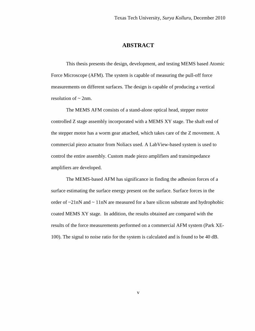
ABSTRACT
This thesis presents the design, development, and testing MEMS based Atomic
Force Microscope (AFM). The system is capable of measuring the pull-off force
measurements on different surfaces. The design is capable of producing a vertical
resolution of ~ 2nm.
The MEMS AFM consists of a stand-alone optical head, stepper motor
controlled Z stage assembly incorporated with a MEMS XY stage. The shaft end of
the stepper motor has a worm gear attached, which takes care of the Z movement. A
commercial piezo actuator from Noliacs used. A LabView-based system is used to
control the entire assembly. Custom made piezo amplifiers and transimpedance
amplifiers are developed.
The MEMS-based AFM has significance in finding the adhesion forces of a
surface estimating the surface energy present on the surface. Surface forces in the
order of ~21nN and ~ 11nN are measured for a bare silicon substrate and hydrophobic
coated MEMS XY stage. In addition, the results obtained are compared with the
results of the force measurements performed on a commercial AFM system (Park XE-
100). The signal to noise ratio for the system is calculated and is found to be 40 dB.

Texas Tech University, Surya Kolluru, December 2010
vi
LIST OF FIGURES
1. Cantilever geometry: a) Bottom View b) Side View[78]
............................................ 8
2. Schematic of Laser Beam Deflection in AFM. ....................................................... 10
3. Optical Lever as a mechanical amplifier. ................................................................ 12
4. Piezo Scanner .......................................................................................................... 14
5. Tripod Scanner. ....................................................................................................... 15
6. Hysteresis Curves of a Piezo Actuator[83]
. .............................................................. 16
7. Piezo scanner depicting the bow motion. ................................................................ 17
8. Feedback loop of an AFM system. .......................................................................... 18
9. Sample tip forces 84
. ................................................................................................. 21
10. Schematic of the vertical tip movement during the approach and retract
cycles of a force spectroscopy experiment. [85]
. .......................................... 23
11. AFM diagram with optical and mechanical components shown. .......................... 25
12. 3-D side angle View of the MEMS AFM. ............................................................. 26
13. 3-D view of stepper motor controlled Z assembly. ................................................ 27
14. Illustration of the cantilever holder assembly. ....................................................... 28
15. Cross-section of SUMMIT V TM process layers showing
Polysilicon and Sacrifical Oxide Layers in µm. 85
...................................... 31
16. (a)AutoCAD layout of the device with important components
highlighted.(b)SEM of the fabricated device 87
. ......................................... 32

Texas Tech University, Surya Kolluru, December 2010
vii
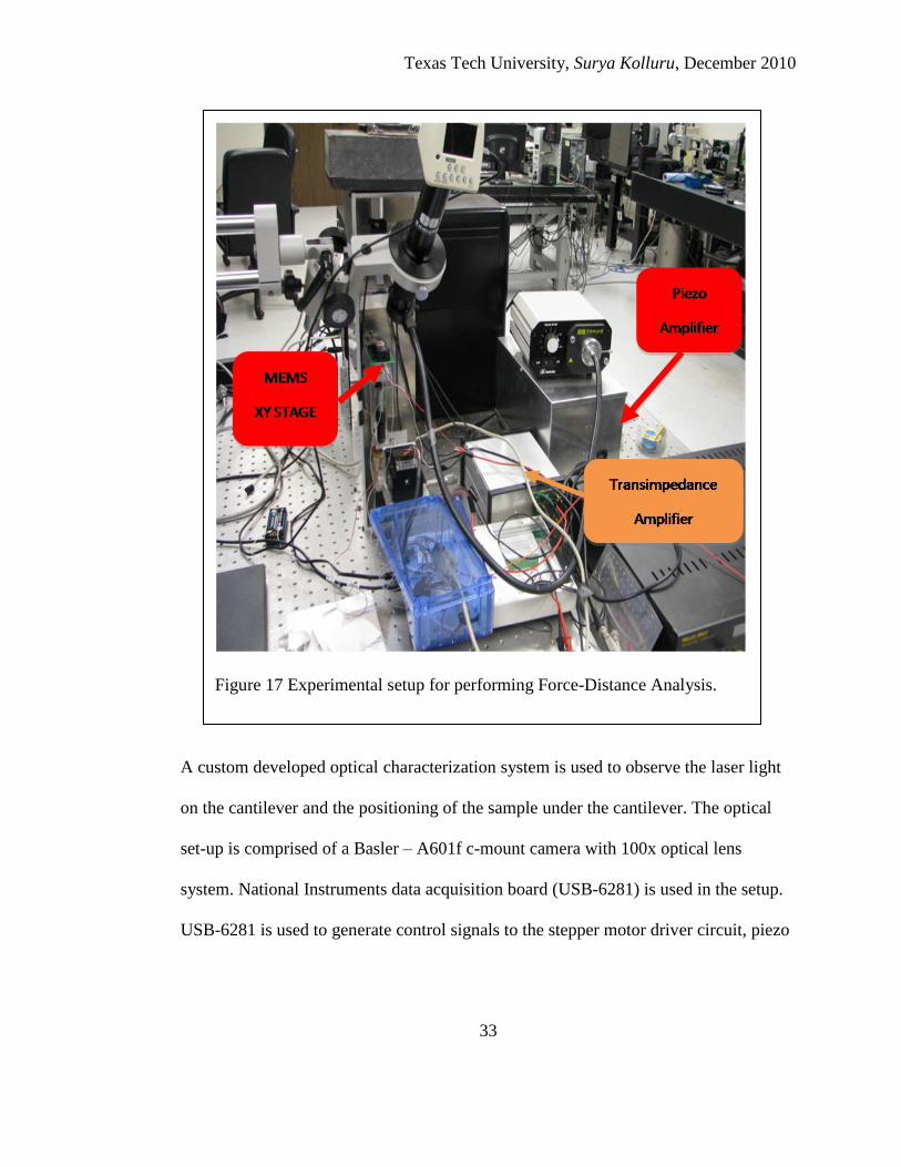
17. Experimental setup for performing Force-Distance Analysis. ............................... 33
18. Screenshot of Labview VI illustrating various controls of the
stepper motor. .............................................................................................. 35
19. Screenshot of Labview VI illustrating various controls in the
Piezo approach segment. ............................................................................. 35
20. Flow-chart illustrating of the flow of sequence in Labview VI ............................. 37
21. Continuation of Flow-chart illustrating of the flow of
sequence in Labview VI. ............................................................................. 38
22. Screenshot of the equivalent circuit of the Piezo Amplifier
drawn in P-Spice. ........................................................................................ 40
23. Frequency Response for the Feedback Zero
Compensation Technique. 88
........................................... 41
24. Screenshot of the equivalent circuit of the Noise
Compensation technique. ............................................................................ 42
25. Frequency response for the Noise Gain compensation
technique.88
.................................................................................................. 43
26. Screenshot of the equivalent circuit of the piezo amplifier
drawn in P-Spice for isolation resistor compensation. ................................ 44
27. Frequency response for the noise gain compensation
technique.88
.................................................................................................. 44
28. Power supply by-passing[89]
. .................................................................................. 46
29. Illustration of ground loops[89]
............................................................................... 47
30. Circuit implementing star-ground approach. [90]
..................................................... 47
31. Illustration of grounding and shielding by using guard rings. ............................... 48

Texas Tech University, Surya Kolluru, December 2010
viii
32. Board layout for transimpedance amplifier............................................................ 49
33. Board layout for the piezo amplifier. ..................................................................... 50
34. Plot of approach and retract curves for contact mode
cantilever and clean mica in air. .................................................................. 52
35. Table indicting the slope of the above linear fit. .................................................... 53
36. Linear fit of the repulsive contact regime. ............................................................. 53
37. Plot of approach and retract curves for contact mode
cantilever and hydrophobic coated surface using MEMS
AFM. ........................................................................................................... 54
38. Plot of approach and retract curves for contact mode
cantilever and hydrophobic coated surface using PARK
XE100 AFM. ............................................................................................... 55
39. Line scan showing pull-off measurements for multiple trials. ............................... 56
40. Pull-off force measurement for a bare silicon substrate using
the MEMS AFM system. ............................................................................ 57
41. Plot of approach and retract curves for contact mode
cantilever and hydrophobic coated surface using Park-
XE100 AFM. ............................................................................................... 58
42. FFT response of the variations of the cantilever at fixed set
point force with the DC component included. ............................................ 59
43. FFT response of the variations of the cantilever at fixed set
point force with the DC component removed. ............................................ 59

Texas Tech University, Surya Kolluru, December 2010
1
CHAPTER I
INTRODUCTION
The technology that deals with the science and engineering of materials at the
dimensions of roughly 1 to 100nm (1 billion nm = 1 m) is called nanotechnology1.
Nanotechnology is a multidisciplinary approach that employs a vast and diverse array
of tools and techniques derived from engineering, physics, chemistry, and biology2.
Recent years have witnessed a substantial growth in the field of nanotechnology, with
increasing need for tools for imaging, measuring and manipulating matter at the
microscale and nanoscale3, 4
. Microscopic imaging has a gigantic influence in industry
and scientific research, especially in the semiconductor industry, surface physics and
various engineering disciplines. Because of these growing demands for investigating
micro-scale and nano-scale samples and the ongoing quest for miniaturization, there
are numerous research methods and instruments for profile and surface inspection.
The significance of this research has been recognized through a number of Nobel
prizes.
The demonstration of the phase contrast method and the subsequent invention
of the Phase Contrast microscope by Zernike earned him the Nobel Prize in 1953
5, 6, 7.
Ruska received the Nobel Prize in 1986 “for his fundamental work in electron optics,
and for the design of the first electron microscope”8, 9
. Scanning tunneling
microscopy10, 11, 12
, invented by Binnig- Rohrer in 1982 which earned them the Nobel
Prize in 1988, is one such tool that has revolutionized micro-scale and nano-scale

Texas Tech University, Surya Kolluru, December 2010
2
imaging and has had a great impact on the technical community by providing a new
and unique tool to advance fundamental science and technology. However, the basic
drawback that it can only image conducting and semiconducting surfaces led to the
invention (Binnig, Quate, and Gerber) of the Atomic Force Microscope (AFM)
through collaboration between IBM and Stanford University in 198613
. Unlike the
electron microscope, which provides a two-dimensional projection or a two-
dimensional image of a sample, the AFM provides a true three-dimensional surface
profile. Since its invention, the atomic force microscope has become a powerful
instrument to measure the surface topography for nanometer scale science and
technology. The ability of the AFM to image at atomic resolution, and the ability to
image a wide variety of specimens (metal semiconductors, soft biological samples,
conductive and non-conductive materials) under wide variety of conditions (air14,15
,
liquid16, 17, 18
, vacuum19,20,21
) have made the AFM a sought after tool in the industry.
The AFM has generated broad technical appeal to the industry with its many powerful,
yet turnkey features.
The operating principle of AFM is based on the measurement of forces of the
order of 10–13
to 10–4
N between the sharp tip attached to the cantilever and the
sample. The forces acting on the tip causes the deflection of the cantilever. A feedback
mechanism is employed to adjust the tip-to-sample distance to maintain a constant
force between the tip and the sample. The different methods that can measure the
deflection of the cantilever include optical-lever22, 23
; electron tunneling 11, 13,24
,
capacitive sensing25
and piezoresistive26, 27
AFM cantilevers. However, the optical

Texas Tech University, Surya Kolluru, December 2010
3
sensor technique exhibits stability and high sensitivity and is simple, robust and small
enough to be integrated into the instrument. The Optical-lever technique proposed by
Meyer and Amer22
in 1988 is most commonly used to measure the deflection of the
probe's cantilever in the AFM. The optical lever operates by reflecting a laser beam
off the back of the cantilever. Angular deflection of the cantilever causes a twofold
larger angular deflection of the laser beam.
1.1 Applications of the Atomic Force Microscope
The remarkable feature of an Atomic Force Microscope (AFM) to “view”
details at the atomic and molecular level has created a niche for itself among
contemporary technologies. New scanning and measurement technologies have
increased the utility of AFM for a broad variety of applications like life science28, 29, 30
,
polymer science31, 32
, electrochemistry33
, biophysics34
, nanotechnology35, 36
and
biotechnology37,38
. These developments have revolutionized AFM in a few short
years, from a laboratory curiosity to one of the most potent, flexible, and widely used
technologies for surface characterization.
The atomic force microscope has the unique capability of imaging biological
samples with molecular resolution and in addition, the forces between single
molecules and the mechanical properties of biological samples can be investigated.
The application of Atomic Force Microscopy(AFM) to biology has provided unique
opportunities to visualize39, 40, 41
and manipulate42, 43, 44
functional biological structures
with nanometer resolution and has enabled researchers to address biological questions
that could not otherwise be investigated. Parot, Dufrene, Hinterdorfer et al.45
reviewed

Texas Tech University, Surya Kolluru, December 2010
4
the history of the AFM in biology and the recent progress made using AFM for
studying cells and cellular interactions, probing single molecules and imaging bio-
surfaces at high resolution. Goksu, Vanegas, Blanchette et al.46
reported the structure
and dynamic measurements of the bio-membranes by AFM. He also designed
experiments, which reveal quantitative details of the mechanisms and factors
controlling vesicle rupture, domain shape and size, phase transformations, and some
model biological interactions in the bio-membranes. Kaminskyj et al.47
showed the use
of AFM for probing the ultra structure, chemistry, physical characteristics and motion
of fungal cells. Lu, Li, An et al.48
focused on focus on the recent development of the
manipulation of single DNA molecules based on atomic force microscopy.
The AFM is fast becoming a powerful characterization tool for polymer
science to visualize and image various materials and their respective surface structures
with superior spatial resolution. The AFM can be used for patterning polymers49,50,51,52
in nanoscale, selective removal of polymer thin films53
and material analysis54
.
Schonherr, Tocha and Vancso55
reported how the atomic force microscope can
quantitatively address friction and in particular surface dynamics of the polymers at
the nanoscale. Hua, King and Henderson 56
showed the patterning of PMMA thin
films using a heated atomic force microscope probe for use as a masking layer in area
selective atomic layer deposition process. Nelson, King et al.57
has described the
deposition of continuous metal nanostructures onto glass and silicon using a heated
atomic force microscope cantilever.
The AFM also finds various applications in electrochemistry58
. It can be used

Texas Tech University, Surya Kolluru, December 2010
5
to study surface structure, properties, and reactivity of the electrode surface at the
electrochemical interface. Studies may be conducted in situ; imaging surfaces in an
electrochemical solution or ex situ, imaging surfaces before and after the electrode is
exposed to the electrolyte solution. In situ AFM measurement has been used to study
the electrochemical deposition of conducting polymers such as poly (o-
methoxyaniline)59
, polybithiophene60
and polypyrrole61
, but mainly focused on the
polymer morphology changes under different polymerization conditions 62
.
The relentless miniaturization of electronic devices and circuits advances
toward the nanometer length scale has demanded the industry to look for alternative
characterization and failure analysis tools. The remarkable feature AFM to offer
enhanced spatial resolution combined with limitations of the other optical
characterization techniques 63, 64
has allowed the AFM to be used for patterning very
discreet features in the field of micro/nano electronics and real space profiling of
electrostatic potential variations in nanoscale electronic devices. Nakamura 65
et al.
reported that AFM conductive probes can be used to study the field-effect transistor
(FET) characteristics of isolated copper phthalocyanine (CuPc) nano-crystals. Koet
al.66
reported the fabrication of single-channel superconducting flux flow transistor
(SSFT) using AFM lithography.
Data storage requires creating structures with nanometer-sized indentations.
The AFM technique finds applications in lot of probe based storage technologies.
Various probe-based techniques have been brought forward ((Cooper et
al.67
,Vettigeret al.68
, Shin et al69
, Bhushan and Kwak70,71
).Various recording

Texas Tech University, Surya Kolluru, December 2010
6
techniques using thermo mechanical (Mamin and Rugar72
,Vettigeret al.68
), phase
change (Gidon et al.73
, Wright et al.74
), magnetic (Ohkubo et al.75
), electrical (Barrett
and Quate76
) and ferroelectric (Franke et al.77
) methods have been demonstrated. The
AFM can be used for high density data storage by writing information as nanometer-
sized indentations into a polymer substrate. IBM has developed a high-density data
storage technology that uses an array of scanning probes (Millepede) for thermo
mechanical recording and playback on an about40 nm thick polymer with a harder Si
substrate (Vettiger et al.68
).
The science, technology, and applications of AFM will continue to be
advanced in the future. The path to commercial success or even laboratory success is
not straightforward. The most significant barriers include the design of high speed
AFM (enhancing the scanning speed of the scanner and increasing the bandwidth of
the feedback loop) that leads to high-throughput and nanometer-resolution imaging.
1.2 Objective
The main objective of this project is to develop a MEMS Atomic Force
Microscope; utilizing the raster scanning feature of the two-axis XY-stage developed
using Sandia‟s SUMMIT V fabrication process. The MEMS Atomic Force
Microscope consists of a standalone optical head, stepper motor controlled Z stage
assembly for bringing the XY stage underneath the cantilever. The feedback for the
AFM, the approach mechanism for the stepper motor and the data acquisition from the
photodetector are all done through National Instruments LabView software.

Texas Tech University, Surya Kolluru, December 2010
7
CHAPTER II
THEORETICAL BACKGROUND
In this chapter we discuss the background of Atomic Force Microscope and its various
modes of operation. We shall also see the various sensing mechanisms used for
quantifying the cantilever deflection.
2.1 Atomic Force Microscope
The Atomic Force Microscope is a characterization tool that can be used to
manipulate and image matter at the nanoscale. The principle of AFM is based on an
atomically sharp tip mounted on a soft cantilever spring that scans over the surface.
The sharp tip interacts with the sample surface sensing the local forces between the tip
and the sample. The most characteristic property of the AFM is that the images are
acquired by 'feeling' the sample surface and the sample
Topography can be recorded with good resolution. The main components of AFM are:
1) AFM probe- a sharp tip mounted on a cantilever.
2) Optical lever system that measures cantilever deflections
3) Feedback loop that allows for monitoring the interaction forces between the tip
and the surface.
4) The piezoelectric scanner that moves the tip relative to the sample in a 3D
pattern.
5) The data acquisition system for acquiring the data and converting the raw data
into topography.

Texas Tech University, Surya Kolluru, December 2010
8
2.1.1 AFM Probes
In this section the material and geometrical properties of a cantilever used in
Atomic Force Microscopy are explained. Being the most sensitive part of the AFM,
the tip that interacts with the surface plays a crucial role in the system. The most
common probes are micro-fabricated using Silicon and Silicon Nitride. Another
material used in cantilever manufacturing is a polymer called SU-8. IBM invented the
near-UV negative photoresist SU-8 78
. The properties and the dimensions of the probe
determine the sensitivity and the resolution of the system. High flexibility and low
stiffness play a crucial role as cantilever with these characteristics exert lesser
downward forces on the sample, and as a result, cause less contortion and damage to
the sample. The resonant frequency of a cantilever is given by
(2.1)
Where k is the spring constant and mo is the effective mass.
The equation states that cantilever can have high resonant frequency and low spring
constant if it has lower mass. The geometry of the cantilever is shown in Figure 1.
(a) (b)
Figure 1Cantilever geometry: a) Bottom View b) Side View[78]
Texas Tech University, Surya Kolluru, December 2010
9
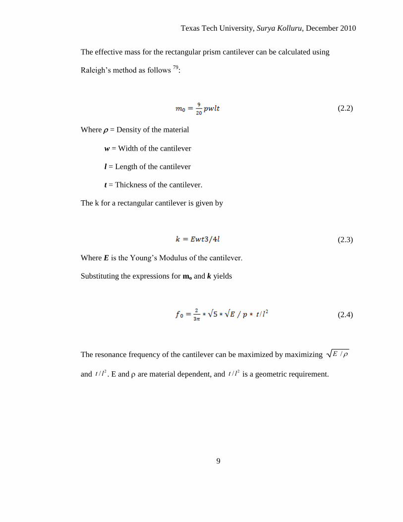
The effective mass for the rectangular prism cantilever can be calculated using
Raleigh‟s method as follows 79
:
(2.2)
Where = Density of the material
w = Width of the cantilever
l = Length of the cantilever
t = Thickness of the cantilever.
The k for a rectangular cantilever is given by
(2.3)
Where E is the Young‟s Modulus of the cantilever.
Substituting the expressions for mo and k yields
(2.4)
The resonance frequency of the cantilever can be maximized by maximizing
E /
and
t / l2 . E and are material dependent, and
t / l2 is a geometric requirement.

Texas Tech University, Surya Kolluru, December 2010
10
2.1.2 Optical Lever
The Atomic Force Microscope measures the deflection of the cantilever at each
point of the scanning area to estimate the changes in surface topography. The optical
lever method proposed by Meyer and Amer is the most commonly used technique of
detecting the cantilever deflection22
. A laser beam is reflected off the back end of the
cantilever onto a quadrant photodetector. The quadrant photodetector senses the
changes in intensity from the reflected laser beam due to the bending of the cantilever
caused by the tip-sample interactions. The difference between the photodiode signals
indicates the position of the laser spot, and thus the angular deflection of the
cantilever.
The system works on the principle of optical-lever where a small deflection of
the cantilever is amplified to a larger displacement on the photodetector. The detection
method is shown in Figure 2.
Deflection of
Figure 2 Schematic of Laser Beam Deflection in
AFM.
Texas Tech University, Surya Kolluru, December 2010
11
the cantilever can be calculated from the individual photocurrents or voltages of the
quadrant photodetector. If the light moves between the upper and lower
or the left and right pairs of the quadrant photodetector, the voltages can be calculated
as follows:
VVertical= (Vupperleft + Vupperright) - (Vlowerleft + Vlowerright )
VHorizontal= (Vupperleft + Vlowerleft) - (Vupperright + Vlowerright)
When the cantilever is in contact with the surface during the scan, the vertical
deflections are used to measure the surface changes in the vertical direction, and if the
horizontal deflections are considered; a more accurate image of the surface topography
is obtained.
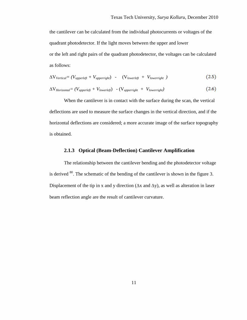
2.1.3 Optical (Beam-Deflection) Cantilever Amplification
The relationship between the cantilever bending and the photodetector voltage
is derived 80
. The schematic of the bending of the cantilever is shown in the figure 3.
Displacement of the tip in x and y direction (x and y), as well as alteration in laser
beam reflection angle are the result of cantilever curvature.

Texas Tech University, Surya Kolluru, December 2010
12
The radius of curvature R of a cantilever is a measure of bending is given by
Where E = Young‟s Modulus
ν = Poisson‟s ratio
τ = Thickness of the cantilever
R = Bending radius of the cantilever.
From the above figure, the actual cantilever displacement x is transformed into
displacement d on the photodetector. As all the angles are very small, it can be
assumed the bending angle of the cantilever is equal to half of the angle of the
deflected laser beam, /2. Therefore, the bending angle of the cantilever is given as
(2.8)
Figure 3 Optical Lever as a mechanical amplifier.

Texas Tech University, Surya Kolluru, December 2010
13
Where L is the distance between the photodetector and the cantilever.
The actual cantilever deflection
x is calculated from the cantilever length
l and the
bending angle of the cantilever is given by
(
Combining the above two equations, the actual cantilever deflection is given by
The relation between the radius of curvature and the deflection angle is
And after substitution,
2.1.4 Piezoelectric Scanner
The piezoelectric scanners are made from piezoelectric crystals that are used
for precise relative motion between the tip and the sample. The piezoelectric crystals
expand or contract proportionally with an applied voltage. The scanner is constructed
By stacking three independent piezoelectric crystals, each of them being responsible
for movements on the X, Y & Z axes respectively. The piezoelectric scanners produce
good reproducibility for smaller displacements, but for larger displacements
(displacements greater than 70%) the piezo response is non-linear (hysteresis). The
Hysteresis can be corrected by closed loop' feedback systems which independently
monitor the scanner movement and correct its motion.

Texas Tech University, Surya Kolluru, December 2010
14
One commonly used design solution is a scanner configuration consisting of a
hollow tube with X & Y axis controlled by two segments of piezoelectric crystal, and
the other segment for moving the tip in Z direction81,82
. Another solution is using a
single piezo cylinder responsible for moving in all the three directions (X, Y & Z
directions) as shown in Figure 4. An X-Y-Z piezo cylinder has five electrodes: four
segment electrodes on the outer surface and one electrode on the inner side of the tube.
There are two types of scanning configurations: Scanned tip AFM where the piezo
scanner is rigidly attached to the probe and is scanned over the sample which remains
stationary and scanned sample AFM where the scanner is attached to the sample and is
moved under the tip. The advantage with the scanned tip AFM is to equip the
system with temperature controlled and liquid controlled stages. The drawback for this
configuration is that the noise level is higher compared to the scanned sample
Figure 4 Piezo Scanner

Texas Tech University, Surya Kolluru, December 2010
15
AFM. For the scanned sample AFM, the weight of the sample has to be controlled
because it sits on top of the scanner.
A tripod scanner can be used for three-dimensional movement of the tip as
shown in figure 5. The tripod scanner consists of three independently controlled piezo
transducers. Each transducer is made of rectangular piece of PZT metalized on two
sides. The three transducers are often called X piezo, Y piezo and Z piezo. By
applying voltages on the piezo, the rods deform in X, Y & Z linear directions.
The material properties of piezo ceramics cause errors that influence the successful
imaging of the AFM systems 82
.
Figure 5 Tripod Scanner.
Texas Tech University, Surya Kolluru, December 2010
16
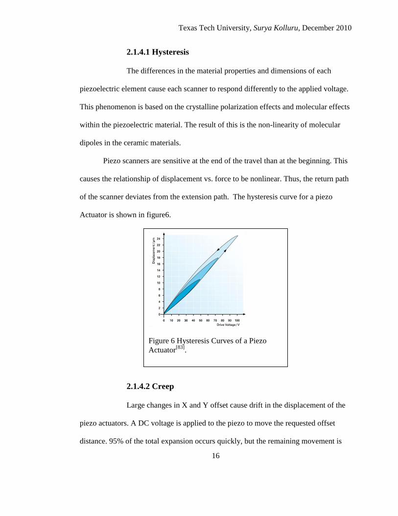
2.1.4.1 Hysteresis
The differences in the material properties and dimensions of each
piezoelectric element cause each scanner to respond differently to the applied voltage.
This phenomenon is based on the crystalline polarization effects and molecular effects
within the piezoelectric material. The result of this is the non-linearity of molecular
dipoles in the ceramic materials.
Piezo scanners are sensitive at the end of the travel than at the beginning. This
causes the relationship of displacement vs. force to be nonlinear. Thus, the return path
of the scanner deviates from the extension path. The hysteresis curve for a piezo
Actuator is shown in figure6.
2.1.4.2 Creep
Large changes in X and Y offset cause drift in the displacement of the
piezo actuators. A DC voltage is applied to the piezo to move the requested offset
distance. 95% of the total expansion occurs quickly, but the remaining movement is
Figure 6 Hysteresis Curves of a Piezo
Actuator[83]
.

Texas Tech University, Surya Kolluru, December 2010
17
slow. The slow portion of the travel is called piezo creep. This will interfere with the
scanning process and distort the image. One way to get around this is to integrate a
capacitor into the drive electronics, which slowly discharges against the trend, keeping
he piezo more or less stationary.
2.1.4.3 Aging
The sensitivity of the piezoelectric materials decreases exponentially
with time. The scanner often needs to be calibrated in the beginning stages as mostly
the changes occur in the scanners early life.
2.1.4.4 Bow
The piezoelectric scanners that move the probe in Atomic Force
Microscope typically move the probe in a curved motion over the surface. This results
in a “Bow” in the AFM image as shown in figure 7. In the tube scanning instruments,
the XY scanner is accomplished by moving the end of the scanner in X & Y
directions.
Figure 7 Piezo scanner depicting the bow
motion.

Texas Tech University, Surya Kolluru, December 2010
18
Translating the Z piezo compensates the Z displacement inherent in swinging an arc.
“Leveling” or “Flattening” the image can compensate the bow in the image.
2.1.5 Feedback System
The main purpose of the feedback system is to regulate the tip-sample distance
by keeping the probe and sample in a fixed relationship while scanning. The constant
contact between the tip and the sample allows for the images to be obtained at lower
forces and without the tip getting damaged.
Typically, a feedback system consists of a three-dimensional piezo crystal that
regulates the movement between the cantilever and the sample, the cantilever and the
photodetector system, and a feedback circuit. The main purpose of the feedback circuit
is to maintain a predefined setpoint that is determined by the instrument gains. The
instrument gains are identified experimentally, the optimal Proportional, Integral, and
Derivative (PID) parameters for each application. Figure 8 shows the schematic of
typical feedback loop in an AFM system.
Figure 8 Feedback loop of an AFM system.

Texas Tech University, Surya Kolluru, December 2010
19
Calculating the difference between the photodetector voltage and pre-defined set point
voltage generates the error signal. The error value is sent as an input for the feedback
calculation. The output of the feedback is given as an input to the high voltage piezo
amplifier, which amplifies the input voltage and sends it to the piezo actuator. The
piezo actuator adjusts accordingly and regulates the tip-sample separation. The
feedback calculation is used to keep the error signal closed to zero. The sample
topography is represented by output of the feedback calculation.
2.2. Imaging Modes
Over the years, different modes of AFM operation have been developed. The different
modes are the following:
2.2.1 Contact Mode Imaging
The most common mode of imaging is the constant force mode. In this mode
the tip is brought in contact with the sample surface, and set to scan the sample in XY
raster pattern. A feedback loop maintains a pre-set constant deflection of the cantilever
with respect to the sample surface by moving the Z scanner for each point of X&Y co-
ordinate. The deflection of the cantilever is caused due to the forces between the tip
and the sample. These forces cause the cantilever to bend according to Hooke‟s law.
(
is the deflection if the cantilever
F is the force acting normal to the cantilever
k is the spring constant of the cantilever.

Texas Tech University, Surya Kolluru, December 2010
20
The scanning speed is limited due to the poor mechanical response of the piezo tube as
it has a resonance frequency of 1 KHz along the Z-axis and resonant frequency of 200-
300 Hz when actuated along the XY plane.
The advantages of this mode are simple operation and direct relation between
the output and the tip-sample forces. The difficulty of measurements taken by this
mode is that the system is more sensitive to noise such as mechanical vibrations and
electrical noise.
The topographical height at the sample at each given point is obtained by the
change in the Z-axis coordinate. By combining the information on all the three axes in
an image called the „height image‟ the 3D image of the sample is obtained.
2.2.2 Tapping Mode Imaging
Contact mode imaging is not an ideal choice for soft samples due to friction
between the AFM tip and the sample. In tapping mode, the cantilever vibrates at its
resonant frequency under an external electrical excitation with amplitude of a few tens
to hundreds of Angstroms. The AFM tip briefly touches the sample at the bottom of
the swing, producing a decrease in oscillation amplitude while raster scanning the
sample in the X -Y directions.
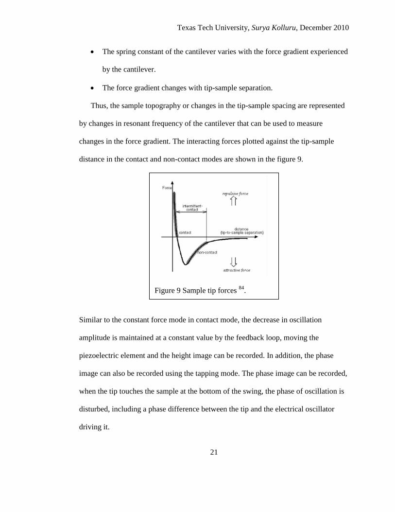
The relationship between the resonant frequency of the cantilever and
variations in sample topography is as follows:
The resonant frequency of the cantilever varies as the square root of its spring
constant.
Texas Tech University, Surya Kolluru, December 2010
21
The spring constant of the cantilever varies with the force gradient experienced
by the cantilever.
The force gradient changes with tip-sample separation.
Thus, the sample topography or changes in the tip-sample spacing are represented
by changes in resonant frequency of the cantilever that can be used to measure
changes in the force gradient. The interacting forces plotted against the tip-sample
distance in the contact and non-contact modes are shown in the figure 9.
Similar to the constant force mode in contact mode, the decrease in oscillation
amplitude is maintained at a constant value by the feedback loop, moving the
piezoelectric element and the height image can be recorded. In addition, the phase
image can also be recorded using the tapping mode. The phase image can be recorded,
when the tip touches the sample at the bottom of the swing, the phase of oscillation is
disturbed, including a phase difference between the tip and the electrical oscillator
driving it.
Figure 9 Sample tip forces 84
.

Texas Tech University, Surya Kolluru, December 2010
22
2.2.3 Friction Imaging
This mode of imaging uses torsional deflection of the cantilever. The
cantilever can measure the friction between the tip and the sample. When the tip
touches the sample, friction occurs and it causes the cantilever to twist. The twisting
motion of the cantilever causes the laser beam to move left and right. The quadrant
photodetector can distinguish the resulting left-and-right motion of the reflected laser
beam from the up-and-down motion from topographic variations. The measured lateral
force provides information on the sample properties, as well as the tip-sample
interaction.
2.2.4 Dynamic Force Spectroscopy mode
In this mode, the cantilever is made to touch the sample and retracted back
over a pre-defined distance in the Z direction. The scan parameters are turned off and
the sample is held at a fixed XY position. As the piezo expands and retracts, the Z
movement of the piezo and the deflection signal from the cantilever are recorded in a
force curve. This may then be repeated at different locations to build up a map of the
tip-surface interaction, or can be repeated at the same point to give a full statistical
understanding of the interaction. These measurements are used to measure nanoscale
contacts, atomic bonding, Vander Waals forces, and single molecule stretching and
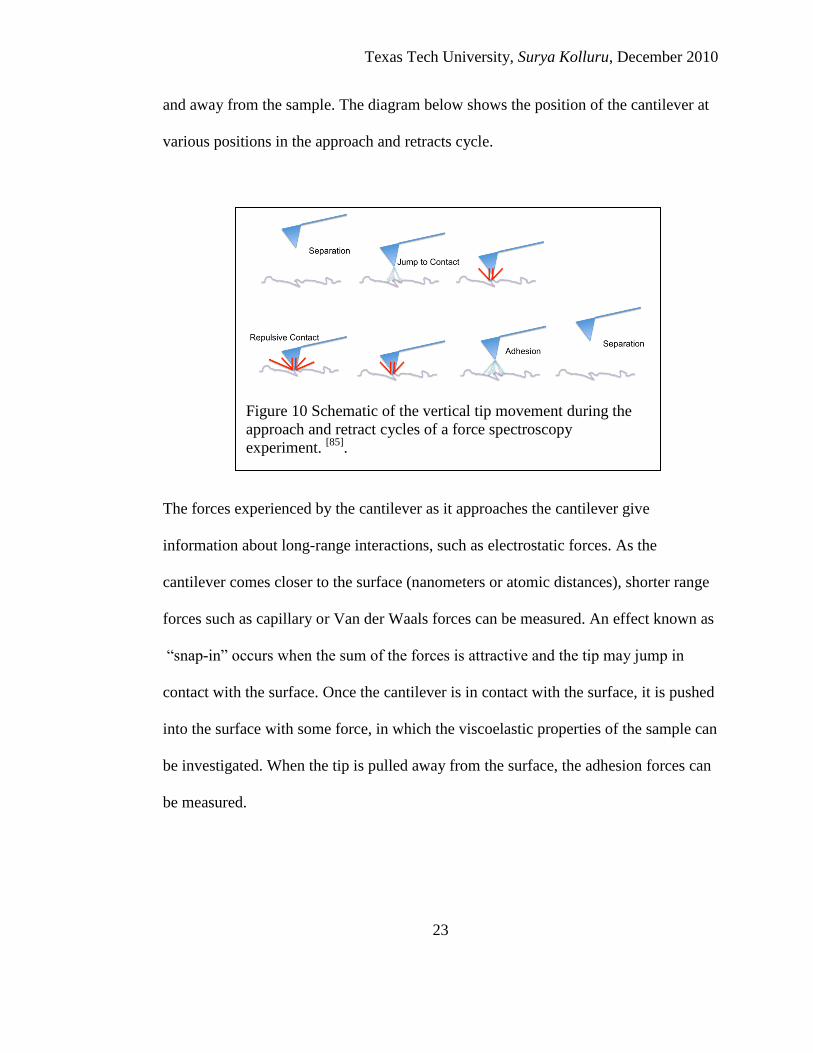
rupture forces. The schematic diagram in Figure 10 shows the movement of the
cantilever and the tip during the force spectroscopy experiment- towards the sample
Texas Tech University, Surya Kolluru, December 2010
23
and away from the sample. The diagram below shows the position of the cantilever at
various positions in the approach and retracts cycle.
The forces experienced by the cantilever as it approaches the cantilever give
information about long-range interactions, such as electrostatic forces. As the
cantilever comes closer to the surface (nanometers or atomic distances), shorter range
forces such as capillary or Van der Waals forces can be measured. An effect known as
“snap-in” occurs when the sum of the forces is attractive and the tip may jump in
contact with the surface. Once the cantilever is in contact with the surface, it is pushed
into the surface with some force, in which the viscoelastic properties of the sample can
be investigated. When the tip is pulled away from the surface, the adhesion forces can
be measured.
Figure 10 Schematic of the vertical tip movement during the
approach and retract cycles of a force spectroscopy
experiment. [85]
.
Texas Tech University, Surya Kolluru, December 2010
24
CHAPTER III
EXPERIMENTAL SETUP
In this chapter, we present the experimental setup used in the design of a
MEMS enabled Atomic Force Microscope. The experimental setup consists of four
main components – Mechanical Assembly, Z Assembly, MEMS XY Stage, and the
electronics for the system. Each of these four components has a detailed description in
this chapter. The chapter also focuses on the design, characterization, and
implementation of these components. Finally, an assembly view of the entire setup is
presented along with an algorithm to operate the system.
3.1 Mechanical Design
The mechanical elements of the MEMS enabled Atomic Force Microscope
(AFM) are documented in this design. The elements of the mechanical assembly of the
instrument are illustrated using three-dimensional solid models made in Autodesk
Inventor. First, the design elements of the Z assembly are addressed and then the
accommodation of the optical head is described. Finally the additional design elements
are presented.
The mechanical assembly primarily consists of four rectangular plates joined
together with set-screws as shown in Figures 11 and 12. The laser diode with the XY

Texas Tech University, Surya Kolluru, December 2010
25
stage is connected to the top plate of the assembly. An angular mount connected to the
sidewall of the mechanical assembly holds the photodetector. The cantilever holder
assembly is connected to the sidewall of the mechanical assembly.
The Z platform sits on a linear translation XY stage and is connected to the
bottom plate of the assembly. The design offers easy access to the optical head and for
replacing the cantilever.
Figure 11 AFM diagram with optical and mechanical components shown.

Texas Tech University, Surya Kolluru, December 2010
26
Figure 12 3-D side angle View of the MEMS AFM.

Texas Tech University, Surya Kolluru, December 2010
27
3.1.1 Z Assembly
The Z stage assembly consists of a stepper motor connected to a worm gear
assembly as shown in Figure 13. The worm gear in turn is connected to a non-rotating
spindle micrometer head, which moves the sample platform in Z direction. A piezo
tube is mounted on the sample platform and the MEMS chip is magnetically attached
to the piezo tube. The stepper motor can be operated in 1/2, 1/4, 1/8, 1/16, 1/32, 1/64
stepping modes. 50 rotations of the motor/worm gear yield 0.5mm movement of the
micrometer. The minimum resolution of the stepper motor controlled Z assembly is
3.3 nm. The ASCII based commands for the stepper motor are given through Labview
interface using the RS 232 communication. The coarser motion (mm) of the stepper
motor brings the MEMS-chip near the vicinity of the cantilever tip. The finer
movement (nm) is accomplished by the Piezo tube.
Figure 13 3-D view of stepper motor controlled Z assembly.
Texas Tech University, Surya Kolluru, December 2010
28
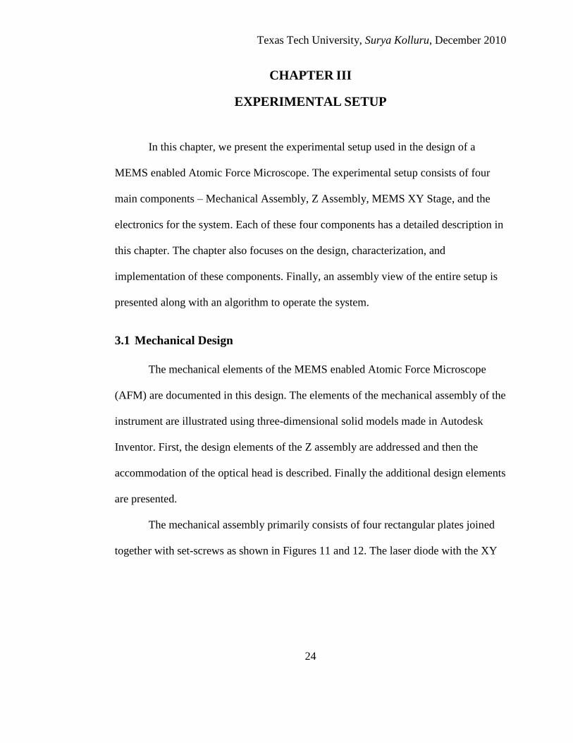
3.1.2 Cantilever Holder Assembly
The cantilever holder consists of three sub-assemblies: A rectangular mount, Z
translation stage and a cantilever angular mount as shown in Figure 14. The
rectangular mount is attached to the main mechanical assembly using precision
screws. The rectangular mount holds the Z translation stage from Newport
Corporation (MS-500-X) with a sensitivity of 0.5 m. The underside of the cantilever
angular mount is etched to accommodate a magnet. The magnet attracts the cantilever
plate and keeps it in place.
Figure 14 Illustration of the cantilever holder assembly.

Texas Tech University, Surya Kolluru, December 2010
29
3.2 MEMS XY stage
Commercially available Scanning Probe Microscopes use piezo scanners for
scanning the sample in 2-axis (X & Y directions). The scan speed is usually limited by
two factors. The first is the fundamental resonance frequency of the scanning element
(usually a piezo element). Secondly, the motion of the piezo element can excite
resonances in the mechanical loop of the scanning probe microscope as a whole. Since
the resolution is very high (10-10
m), any vibration will lower the image quality
significantly.
Microelectromechanical Systems (MEMS) are devices with micrometer-sized
features that perform electronic and mechanical actions. These devices can be
designed to perform SPM-like motion and MEMS SPM devices have been designed
previously by a number of groups. In this project, I have incorporated a bi-directional
Two-Axis Electrostatic MEMS Positioning System, fabricated using the SUMMIT V
fabrication process.
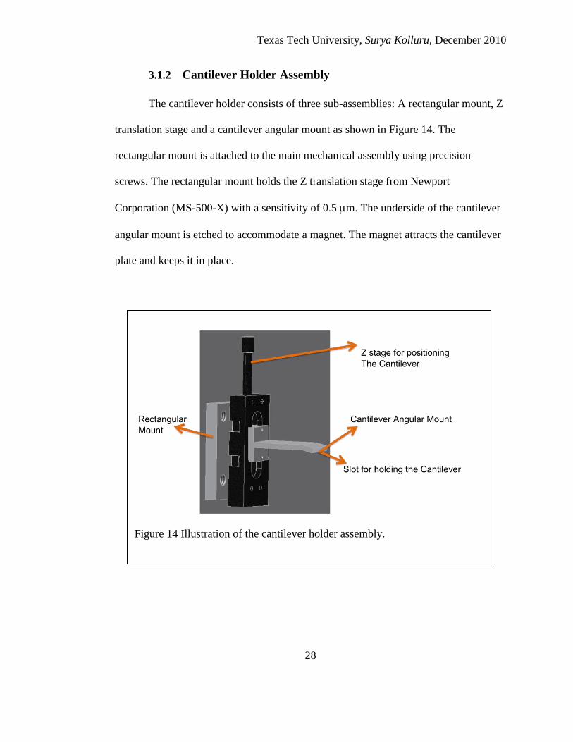
3.2.1 SUMMIT-V Process
SUMMIT- V process is the acronym for Sandia Ultra-planar Multi-level
MEMS fabrication Technology. It is a surface-micromachining process developed by
Sandia National Laboratories featuring four mechanical layers of polysilicon
fabricated above a thin highly doped polysilicon electrical interconnect and ground
plane layer. Figure 15 shows the cross section view of the various structural and
sacrificial layers available in the SUMMiT V process along with their thickness.

Texas Tech University, Surya Kolluru, December 2010
30
The process begins with an n-type, (100) silicon wafer on which a 0.63-μm
layer of silicon dioxide (SiO2) is thermally grown. This layer creates electrical
isolation for the MMPOLY0 layer with the wafer. A 0.8-μm thick layer of low-stress
silicon nitride (Si3N4) is then deposited on top of the oxide layer. The silicon nitride is
used as an etch stop during the wet etch step and it can also be used as extra layer for
electrical isolation. This nitride layer acts like an electrical insulator and also as an
etch stop thus protecting the underlying oxide from wet etchants during processing.
Above the nitride layer, deposit 0.3 m doped poly Si (Poly 0, 28Ω/sq), pattern/etch
with MMPOLY0mask, for mechanical anchor, ground or wiring layer.
Above MMPOLY0, the 1st sacrificial oxide layer (SacOx 1) is deposited,
which is a 2 μm thick conformal layer. A pattern/etch with DIMPLE_CUT mask is
used to form dimples (dimple depth controlled using timed etch 1.5 μm deep). The
SacOx1 layer is patterned a 2nd
time with SACOX1_CUT mask to form anchor sites to
the MMPOLY0 layer. Above MMPOLY0, 1 m of doped poly Si is deposited
conformally (Poly 1, 23Ω/sq).
Above MMPOLY1 is sacrificial oxide layer (SACOX2), this is a thin layer
(0.3μm) that separates MMPOLY1 from MMPOLY2.A pattern/etch with SACOX2
mask is used to define a structure in the layer or with PIN_JOINT_CUT to define a
hub for a rotating member. The gear hubs provide a rotational degree of freedom to
mechanical parts (gears) developed in the SUMMiT process.
Above SACOX2, deposit 1.5 μm of doped poly Si (Poly 2, 22Ω/sq). Some
goes directly onto MMPOLY1 being permanently bonded (~ 2.5 μm thick);
Texas Tech University, Surya Kolluru, December 2010
31
pattern/etch with MMPOLY2. For the layers above MMPOLY2, chemical mechanical
polishing (CMP) is done to planarize the sacrificial oxide layers.
Above MMPOLY2, deposit ~ 6 m of oxide (TEOS process) (SacOx 3)
followed by CMP to planarize. It is Patterned/etched with DIMPLE3_CUT for
dimples (etch through SacOx3) and SACOX3_CUT for anchors. Approximately, 0.4
m poly Si is deposited to backfill dimple holes.
Above the SACOX3 layer, approximately 2 m of doped poly (Poly 3, 8Ω/sq) is
deposited on SACOX3 layer, and patterned/etched with MMPOLY3. Above
MMPOLY3 layer, the oxide layer (SacOx 4) is deposited & patterned/etched with
SACOX4_CUT and DIMPLE4_CUT. Finally, Deposit ~ 2 m doped poly Si
layer(Poly 4) and pattern/etch with MMPOLY4.
Finally, the release of all the exposed oxides is carried out by a 100:1 HF:HCl
Figure 15 Cross-section of SUMMIT V TM process layers showing
Polysilicon and Sacrifical Oxide Layers in µm. 85
Texas Tech University, Surya Kolluru, December 2010
32
wet etch solution. Simple air evaporation or supercritical carbon-dioxide (SCCO)
drying is done to minimize the capillary forces [86].
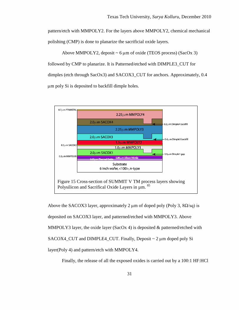
3.2.2 AutoCAD designs for MEMS XY stage
The figure 16 below shows a MEMS bidirectional Two-Axis Electrostatic
MEMS Positioning System fabricated using Sandia‟s SUMMiT V design process.
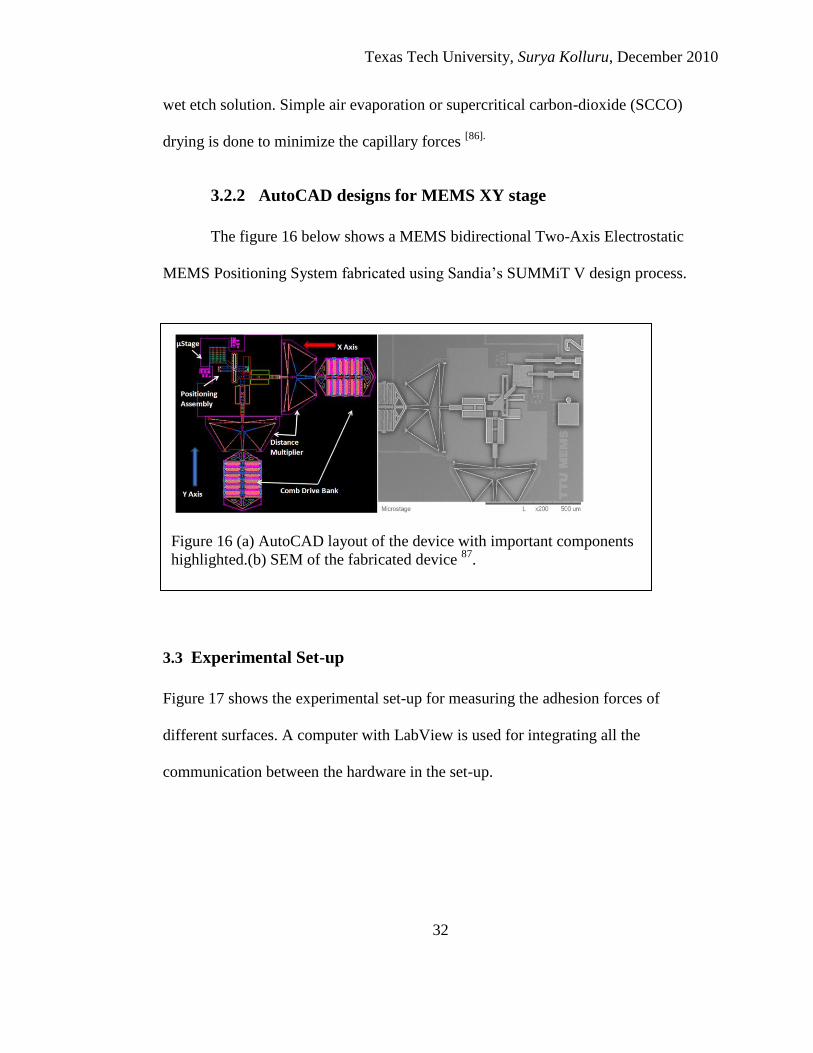
3.3 Experimental Set-up
Figure 17 shows the experimental set-up for measuring the adhesion forces of
different surfaces. A computer with LabView is used for integrating all the
communication between the hardware in the set-up.
Figure 16 (a) AutoCAD layout of the device with important components
highlighted.(b) SEM of the fabricated device 87
.
Texas Tech University, Surya Kolluru, December 2010
33
A custom developed optical characterization system is used to observe the laser light
on the cantilever and the positioning of the sample under the cantilever. The optical
set-up is comprised of a Basler – A601f c-mount camera with 100x optical lens
system. National Instruments data acquisition board (USB-6281) is used in the setup.
USB-6281 is used to generate control signals to the stepper motor driver circuit, piezo
Figure 17 Experimental setup for performing Force-Distance Analysis.
Texas Tech University, Surya Kolluru, December 2010
34
amplifier and to acquire the analog voltage readout from the transimpedance amplifier.
The acquired analog voltage signal is fed to the piezo actuator.
Figure 18 shows the front panel of the LabView Virtual Instrument (VI)
program. This VI is comprised of several segments. In the STEPPER MOTOR
segment, the VI performs the movement of the sample in the Z direction. Another
important feature of the VI is the Step Mode control for the user. The user has the
liberty to choose the step mode from among the microstepping mode options
available. Based on the relative position of the sample with respect to the cantilever,
the user can use any mode based on his/ her needs on the approach mechanism.
Figure 19 shows the front panel of the LabView Virtual Instrument (VI)
program. This VI includes the XY graph for photodiode signal in a quadrant format
replicating the movement of the laser on the photodiode. The other controls include
the SUM signal indicating the laser intensity on the photodiode and the Vpiezo which
indicates the voltage being applied to the piezo tube. The Vpiezo and the
DIFFERENCE signal of the photodiode are written into an excel file for plotting the
data.

Texas Tech University, Surya Kolluru, December 2010
35
The sequence of steps for performing force-distance analysis is given in Figure 20.
Initially, we set the set point voltage to the desired value and the maximum
Figure 18 Screenshot of Labview VI illustrating various controls of the
stepper motor.
Figure 19 Screenshot of Labview VI illustrating various controls in the
Piezo approach segment.

Texas Tech University, Surya Kolluru, December 2010
36
displacement in X direction (Xmax) and maximum displacement in Y direction (Ymax)
values respectively, for the XY stage.
We move the sample towards the cantilever by selecting the coarse approach
mechanism using the stepper motor. Then the control checks if the sample is close
enough to the cantilever or not. If the sample is not close enough, we continue with the
coarse approach, else the user can switch over to the fine approach mode using the
piezo. In the fine approach mode, the piezo displaces by 5 nm and every time the
piezo is displaced, the user can monitor if the Va-b signal on the photodiode is equal to
the set point or not. If the condition is not met the piezo voltage is incremented. If the
condition is met, then the piezo voltage is decremented. Once the decremental voltage
reaches the minimum condition of the piezo, then the stage is displaced by 0.2m.
Then the whole process is repeated again for each value of X & Y until X = Xmax and
Y = Ymax. The data is collected and the force-vs -distance curves are plotted.

Texas Tech University, Surya Kolluru, December 2010
37
Figure 20 Flow-chart illustrating of the flow of sequence in Labview VI.

Texas Tech University, Surya Kolluru, December 2010
38
Figure 21 Continuation of Flow-chart illustrating of the flow
of sequence in Labview VI.
Texas Tech University, Surya Kolluru, December 2010
39
3.4 Op-Amp Design
In this section the design considerations of the piezo amplifier and photodiode
amplifier are discussed.
3.4.1 Piezo Amplifier
A piezo amplifier with a peak voltage rating of 200 V and a peak current of
500 mA was designed. The Apex precision power‟s PB50 and Linear Technologies
LT1007 operational amplifiers are used in this design. Both the amplifiers are
cascaded to form a composite amplifier configuration. The PB50 and LT 1007 are
used as booster amplifier and driver amplifier, respectively. The main advantage with
the power booster included within the feed- back loop of the driver amplifier results in
a composite amplifier with the accuracy of the driver and the extended output voltage
range and current capability of the booster.
The design of composite amplifier requires careful consideration of several
amplifier and system parameters. The most important of these are gain, stability, slew
rate, and output swing of the driver. Operating the booster amplifier in higher gain
results in a higher slew rate and lower output swing requirement for the driver, but
makes stability more difficult to achieve.

Texas Tech University, Surya Kolluru, December 2010
40
3.4.2 Stability for Op-Amp
The stability of the op-amp depends on the phase relationship between the
input and output for the amplifier. If the phase crosses -180° at a frequency where the
gain of the amplifier is less than unity, the amplifier is “unconditionally stable”. To
compensate the amplifier, we add some additional components that shape its
frequency response so that its gain is less than unity by the time the phase hits -
180°.This does, however, compromise the high-frequency response of the amplifier.
Most of the op-amps are internally compensated. However, some op-amps require
external components to make sure that the op-amp remains stable. In this section we
will discuss the various compensation techniques used in designing the Piezo amplifier
to make it stable.
Figure 22 Screenshot of the equivalent circuit of the Piezo Amplifier drawn
in P-Spice.

Texas Tech University, Surya Kolluru, December 2010
41
3.4.2.1 Feedback Zero Compensation
The goal of this compensation technique is to alter the loop gain (1/)
by adding a feedback capacitor CF, which places a pole in the loop so that it intersects
the open loop gain (AOL) line at 20db per decade instead of at 40dB per decade as
shown in Figure 23.
Figure 23 Frequency Response for the Feedback Zero
Compensation Technique. 88
Texas Tech University, Surya Kolluru, December 2010
42
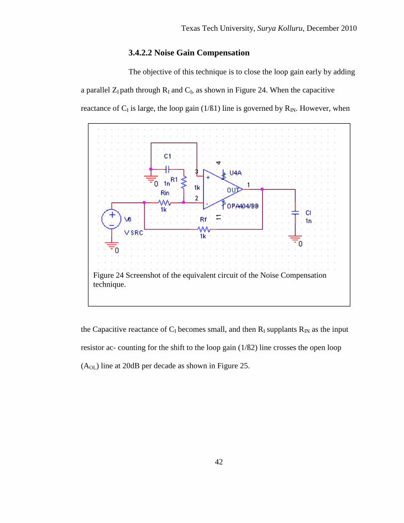
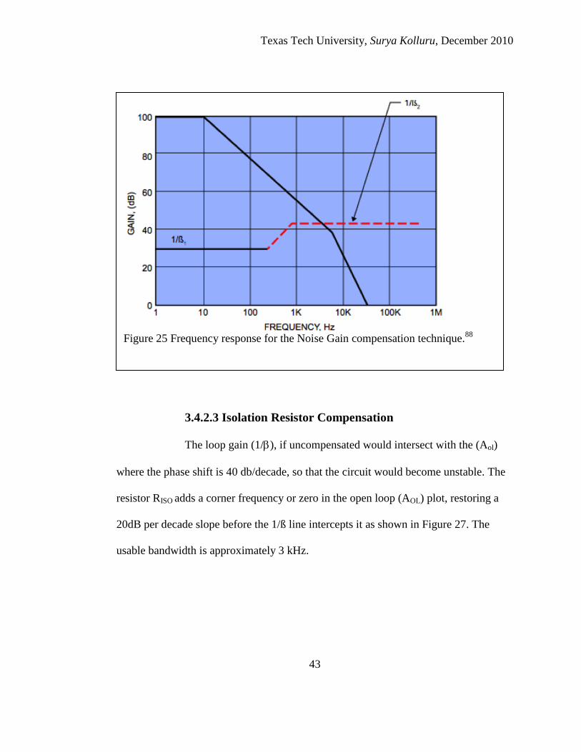
3.4.2.2 Noise Gain Compensation
The objective of this technique is to close the loop gain early by adding
a parallel ZI path through RI and CI, as shown in Figure 24. When the capacitive
reactance of CI is large, the loop gain (1/ß1) line is governed by RIN. However, when
the Capacitive reactance of CI becomes small, and then RI supplants RIN as the input
resistor ac- counting for the shift to the loop gain (1/ß2) line crosses the open loop
(AOL) line at 20dB per decade as shown in Figure 25.
Figure 24 Screenshot of the equivalent circuit of the Noise Compensation
technique.
Texas Tech University, Surya Kolluru, December 2010
43
3.4.2.3 Isolation Resistor Compensation
The loop gain (1/), if uncompensated would intersect with the (Aol)
where the phase shift is 40 db/decade, so that the circuit would become unstable. The
resistor RISO adds a corner frequency or zero in the open loop (AOL) plot, restoring a
20dB per decade slope before the 1/ß line intercepts it as shown in Figure 27. The
usable bandwidth is approximately 3 kHz.
Figure 25 Frequency response for the Noise Gain compensation technique.
88

Texas Tech University, Surya Kolluru, December 2010
44
3.5 PCB Design
In a system that measures deflections in the low nanometer range, the design of
the printed circuit board (PCB) poses a challenge. The results in the above discussion
are based on PSPICE simulations and do not take into account on-board parasitic that
Figure 26 Screenshot of the equivalent circuit of the piezo amplifier
drawn in P-Spice for isolation resistor compensation.
Figure 27 Frequency response for the noise gain compensation
technique.88

Texas Tech University, Surya Kolluru, December 2010
45
play a vital role in morphing the actual signal. Beside circuit simulations, prototyping
on a copper board or a breadboard is of utmost importance to get a measure of the
parasitic capacitances and noise effects introduces due to circuit components and trace
lines. The following steps were included in the final PCB design to reduce the effect
of parasitic and to reduce unwanted oscillations in the circuit:
3.5.1 Power Supply Bypassing
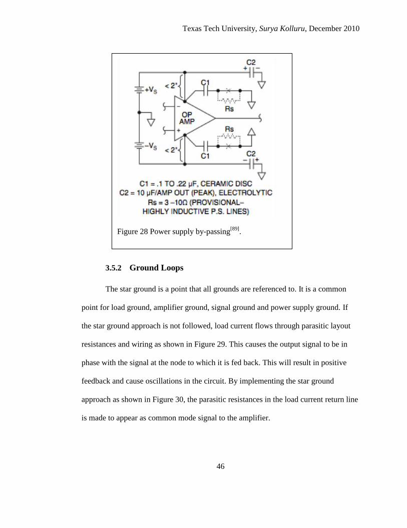
Bypassing the power supply at the amplifier‟s supply terminals is a critical
aspect of PCB design. Each supply pin must be bypassed to common with a “high
frequency bypass” 0.1uF to 0.22uF ceramic capacitor. These capacitors must be
located directly at the power op amp supply pins. In rare cases where power supply
line inductance is high, it may be necessary to add 1 to 10 ohms of resistance in series
with the high frequency bypass capacitor to dampen the Q of the resultant LC tank
circuit as shown in figure 28.
In addition, a “low frequency bypass” capacitor, minimum value of 10uF per
Ampere of peak output current, should be added in parallel with the high frequency
bypass capacitors from each supply rail to common. Tantalum capacitors should be
used when possible due to their low leakage, low ESR and good thermal
characteristics. Aluminum Electrolytic capacitors are acceptable for operating
temperatures above 0°C. These capacitors should be located within 2" of the power op
amp supply pins.
Texas Tech University, Surya Kolluru, December 2010
46
3.5.2 Ground Loops
The star ground is a point that all grounds are referenced to. It is a common
point for load ground, amplifier ground, signal ground and power supply ground. If
the star ground approach is not followed, load current flows through parasitic layout
resistances and wiring as shown in Figure 29. This causes the output signal to be in
phase with the signal at the node to which it is fed back. This will result in positive
feedback and cause oscillations in the circuit. By implementing the star ground
approach as shown in Figure 30, the parasitic resistances in the load current return line
is made to appear as common mode signal to the amplifier.
Figure 28 Power supply by-passing[89]
.

Texas Tech University, Surya Kolluru, December 2010
47
Figure 29 Illustration of ground loops[89]
Figure 30 Circuit implementing star-ground
approach. [90]
Texas Tech University, Surya Kolluru, December 2010
48
3.5.3 Grounding and Shielding
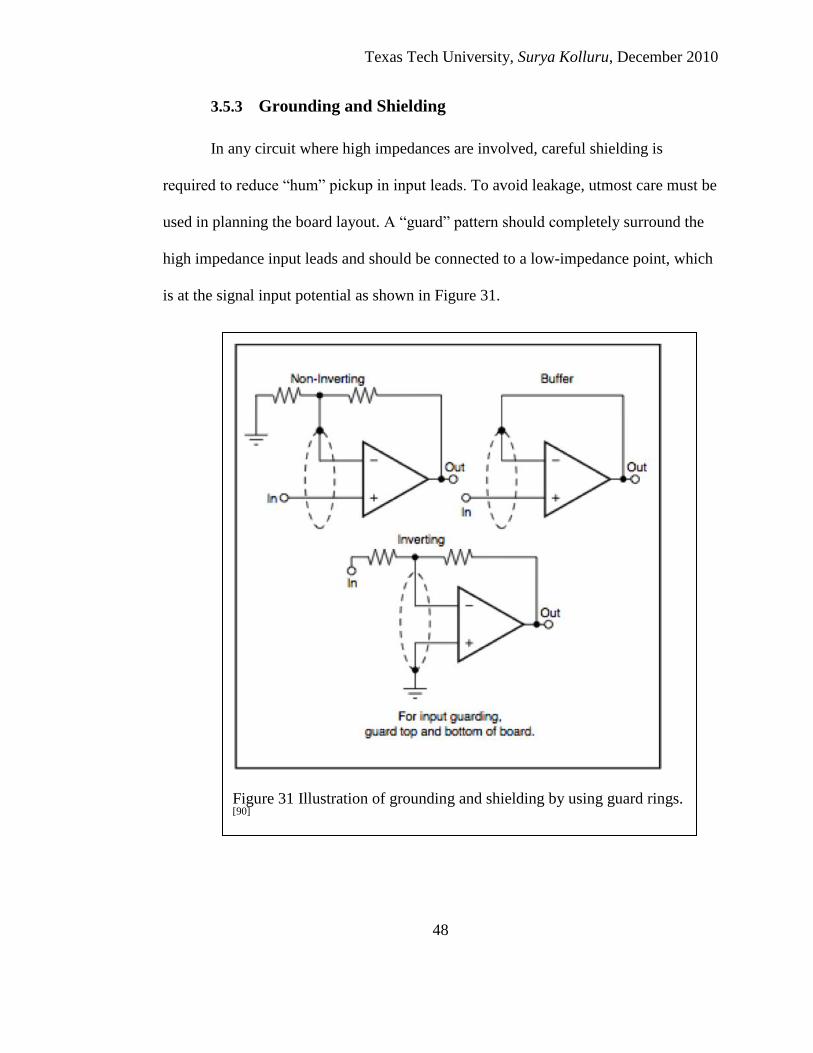
In any circuit where high impedances are involved, careful shielding is
required to reduce “hum” pickup in input leads. To avoid leakage, utmost care must be
used in planning the board layout. A “guard” pattern should completely surround the
high impedance input leads and should be connected to a low-impedance point, which
is at the signal input potential as shown in Figure 31.
Figure 31 Illustration of grounding and shielding by using guard rings. [90]

Texas Tech University, Surya Kolluru, December 2010
49
The board layout for the amplifiers was done using the 4PCB artist software.
The boards include 2 layer boards for the transimpedance amplifier and piezo
amplifier.
Figure 32 Board layout for transimpedance amplifier.

Texas Tech University, Surya Kolluru, December 2010
50
3.6 Conclusions
This chapter describes the mechanical and electrical design of the MEMS Atomic
Force Microscope (AFM). The experimental setup consists of four main components -
Mechanical Assembly, Z Assembly, MEMS XY Stage, and the electronics for the
system. Each of the subsystems has been explained in detail. The sequence of steps
involved in the operation of the stepper motor controlled Z assembly and the
photodiode acquisition are explained in detail using flow charts.
Figure 33 Board layout for the piezo amplifier.

Texas Tech University, Surya Kolluru, December 2010
51
CHAPTER IV
EXPERIMENTAL RESULTS AND FUTURE WORK
This chapter discusses the results of adhesion force measurements of various samples.
First, the optical lever sensitivity of the MEMS AFM is characterized and explained.
Second, the adhesion force measurements of hydrophobic and silicon-substrate are
reported. In the force measurements for silicon substrate and mica, the sample is
placed on a glass substrate, which is glued to the MEMS packaged chip. The
mechanical XY stage is used to position the sample underneath the cantilever.
After the discussions of various measurements, possible future work for improving the
setup to obtain 3-D topography is explained.
4.1 Calibration of Cantilever Deflection
The conversion of the photodetector signal into a quantitative of force requires
two measurements. The first stage is to calibrate the distance that the cantilever
actually deflects for measured change in photodiode voltage. This value depends on
the dimensions of the cantilever, and the optical path of the AFM detection laser. The
deflection of the cantilever is given by δ; the spring constant of the cantilever can be
used to convert this value into force using the Hooke‟s Law formula:
(
Where
F = Force measured in nN

Texas Tech University, Surya Kolluru, December 2010
52
k = Spring constant of the Cantilever
δ = Sensitivity (V/nm) of the Optical Lever
A force curve between a plain cantilever tip and a hard mica substrate is used to
determine the sensitivity of the experimental set-up as shown in Figure 34. The
sensitivity is the measurement of the deflection of the tip in nanometers for a given
moment of detection of laser on the photodiode. The sensitivity is calculated by
taking into account the gradient of the repulsive contact region.
Figure 34 Plot of approach and retract curves for contact mode
cantilever and clean mica in air.
Texas Tech University, Surya Kolluru, December 2010
53
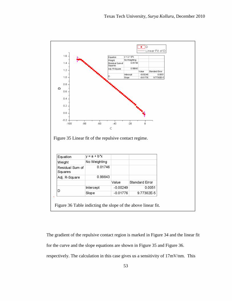
The gradient of the repulsive contact region is marked in Figure 34 and the linear fit
for the curve and the slope equations are shown in Figure 35 and Figure 36.
respectively. The calculation in this case gives us a sensitivity of 17mV/nm. This
Figure 35 Linear fit of the repulsive contact regime.
Figure 36 Table indicting the slope of the above linear fit.

Texas Tech University, Surya Kolluru, December 2010
54
value can be used to convert the deflection data along the whole curve into
nanometers.
4.2 Adhesion Force Measurements for Hydrophobic Coatings
Adhesion force measurements are performed on a hydrophobic coated MEMS XY
stage as shown in Figure 37.
Figure 37 shows the force-distance plot for a hydrophobic coated MEMS XY stage.
The MEMS XY stage is brought in contact with the cantilever and then retracted back.
The deflection (nm) vs. height (nm) values is stored in an Excel file in LabView. The
deflection values are converted to suitable forces using equation 4.1. The cantilever
Figure 37 Plot of approach and retract curves for contact mode
cantilever and hydrophobic coated surface using MEMS AFM.
Texas Tech University, Surya Kolluru, December 2010
55
used in this experiment is CSG10 which has a spring constant of 0.974 N/m. The true
interaction force value is found by subtracting the baseline from all deflection data.
The least value of the force on the force-distance curve indicates the adhesion force
present on the hydrophobic coated MEMS stage. In order to make sure that the
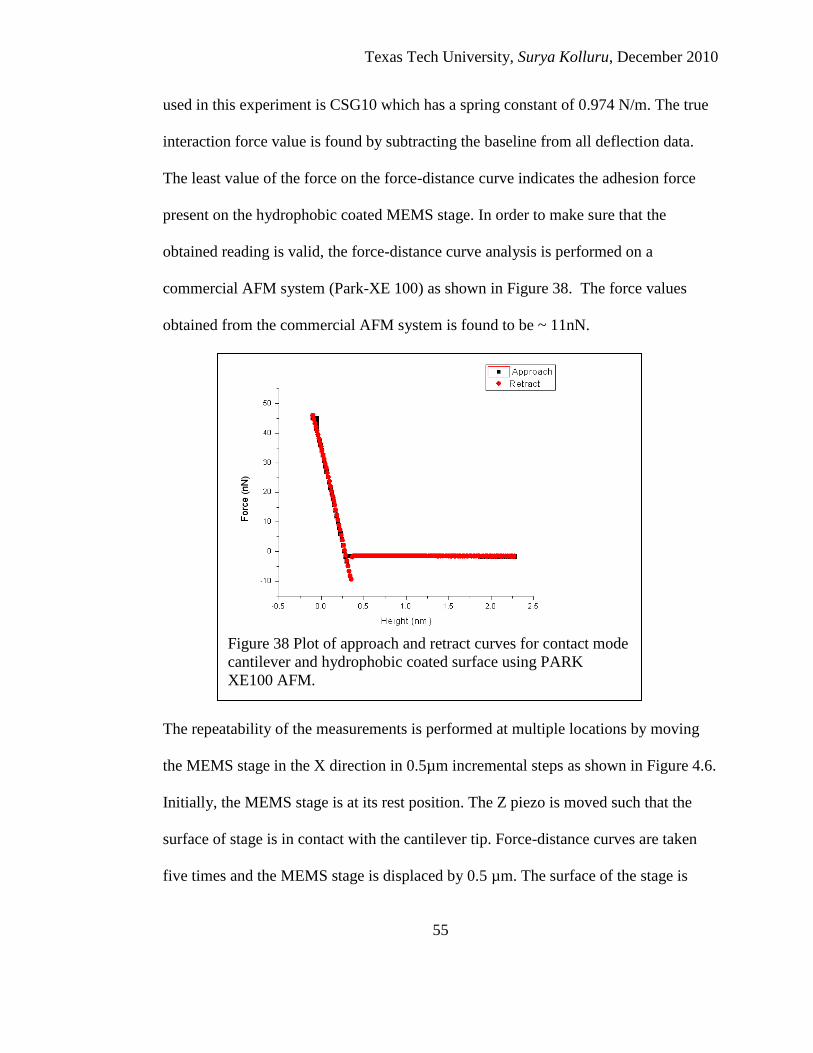
obtained reading is valid, the force-distance curve analysis is performed on a
commercial AFM system (Park-XE 100) as shown in Figure 38. The force values
obtained from the commercial AFM system is found to be ~ 11nN.
The repeatability of the measurements is performed at multiple locations by moving
the MEMS stage in the X direction in 0.5µm incremental steps as shown in Figure 4.6.
Initially, the MEMS stage is at its rest position. The Z piezo is moved such that the
surface of stage is in contact with the cantilever tip. Force-distance curves are taken
five times and the MEMS stage is displaced by 0.5 µm. The surface of the stage is
Figure 38 Plot of approach and retract curves for contact mode
cantilever and hydrophobic coated surface using PARK
XE100 AFM.

Texas Tech University, Surya Kolluru, December 2010
56
again approached and retracted from the cantilever tip. This whole process is repeated
until the stage displaces by 2.5µm in the X direction as shown in Figure 39.
4.3 Adhesion Force Measurements for Silicon Substrate
The pull-off force measurements for a bare silicon substrate are performed as
shown in Figure 40. For a bare silicon substrate, the adhesion forces are stronger than
the hydrophobic coated MEMS stage. The experiment is performed on a glass
substrate which is glued to the MEMS packaged chip. The positioning of the silicon
substrate under the cantilever is done using the Newport Precision 460p series manual
XY stage. The adhesion values of the silicon substrate is found to be ~ 21 nN, twice
the value of the hydrophobic coated MEMS stage.
Figure 39 Line scan showing pull-off measurements for multiple
trials.

Texas Tech University, Surya Kolluru, December 2010
57
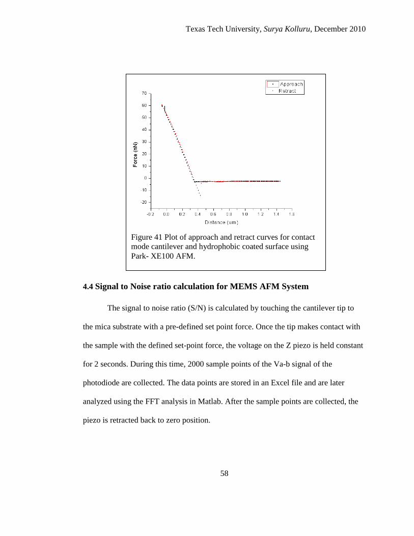
Figure 41 shows the pull off force measurements using a Park-XE 100 AFM.
The adhesion force for the silicon substrate is found to be 18nN, which closely
matches with the value, obtained using the MEMS AFM system.
Figure 40 Pull-off force measurement for a bare silicon
substrate using the MEMS AFM system.
Texas Tech University, Surya Kolluru, December 2010
58
4.4 Signal to Noise ratio calculation for MEMS AFM System
The signal to noise ratio (S/N) is calculated by touching the cantilever tip to
the mica substrate with a pre-defined set point force. Once the tip makes contact with
the sample with the defined set-point force, the voltage on the Z piezo is held constant
for 2 seconds. During this time, 2000 sample points of the Va-b signal of the
photodiode are collected. The data points are stored in an Excel file and are later
analyzed using the FFT analysis in Matlab. After the sample points are collected, the
piezo is retracted back to zero position.
Figure 41 Plot of approach and retract curves for contact
mode cantilever and hydrophobic coated surface using
Park- XE100 AFM.

Texas Tech University, Surya Kolluru, December 2010
59
Figure 42 shows the FFT response of the FFT response of the variations of the
cantilever at fixed set point force with the DC component included. The DC
component gives the signal magnitude and is found to be 262 units.
Figure 42 FFT response of the variations of the cantilever at fixed set
point force with the DC component included.
Figure 43 FFT response of the variations of the cantilever at fixed set
point force with the DC component removed.

Texas Tech University, Surya Kolluru, December 2010
60
Figure 43 shows the FFT response of the variations of the cantilever at fixed set point
force with the DC component removed. The DC component is removed by subtracting
the mean of the sample points from each individual point. The maximum noise peak is
found to be 7.8 units. The noise spectrum includes all non-fundamental spectral
components in the Nyquist frequency range (sampling frequency / 2) without the DC
component, the DC component, and the harmonics: The signal to noise ratio is
calculated using the formula:
(4.2)
The SNR for the MEMS AFM systems was found to be 40dB.
The RMS variations of the cantilever deflection are calculated by the square root of
the arithmetic mean (average) of the squares of the original values. The RMS variation
is found to be 2nm.
4.5 Future Work
1. Obtain a 3-D topography by utilizing an electrothermal MEMS stage as the
electrostatic actuator causes the cantilever to snap down due to the potential
difference between the MEMS stage and the cantilever.
2. Pull-off force measurements for other various self-assembled mono layer
coated MEMS devices.
3. Reducing the overall size of the system such that there would be minimum
mechanical vibrations in the system.

Texas Tech University, Surya Kolluru, December 2010
61
CHAPTER V
CONCLUSION
This thesis demonstrates the design, development, and operation of MEMS Atomic
Force- Microscope integrated with a bi-directional two-axis MEMS positioning
system. The MEMS AFM consists of a stand-alone optical head, stepper motor
controlled Z assembly. Commercial Piezo actuator is used along with stepper motor
coupled worm gear assembly to provide micro-step motion. National Instruments data
acquisition cards (USB-6281) are utilized in conjunction with LabView to provide
control of the stepper motor. The signals from the photodiode are collected using the
data acquisition card and sent to the Labview Interface.
The pull-off force measurements for different surfaces are demonstrated.
Surface forces in the order of 21 nN and 11 nN are measured for a bare silicon
substrate and hydrophobic coated MEMS stage. The repeatability of the force
measurements is performed to see the variations in the adhesion force values.
The signal to noise ratio for the system is calculated to be 40dB. The RMS variations
of the cantilever deflection are found to be 2 nm. Possible improvements are specified
that can be implemented in the system to obtain 3-D topography.

Texas Tech University, Surya Kolluru, December 2010
62
REFERENCES
[1] "Nanotechnology: Big Things from a Tiny World", Nano Technology
Initiative [Online]. Available from http://www.nano.gov/
[2] S. K. Sahoo, S. Parveen, and J. J. Panda, “The present and future of
nanotechnology in human health care”, Nanomedicine-Nanotechnology
Biology and Medicine, vol. 3, no. 1, pp. 20-31, Mar, 2007.
[3] J.A. Dagata, J. Schneir, H.H. Harary, C.J. Evans, M.T. Postek, J.Bennett,
“Modification of hydrogen‐passivated silicon by a scanning tunneling
microscope operating in air”, Appl. Phys. Lett, vol. 56 , pp. 2001-2003. 1990.
[4] E.S. Snow, P.M. Campbell, “Fabrication of Si nanostructures with an atomic
force microscope”, Appl. Phys. Lett. vol. 64, pp. 1932-1934, 1994.
[5] F. Zernike, “Diffraction theory of the knife-edge test and its improved form,
the phase-contrast method”, Royal Astronomy Society Monthly Notices, vol.
94, pp. 377-384, 1934.
[6] F. Zernike, “Phase-contrast, a new method for microscopic observation of
transparent objects. Part I”, Physica, vol. 9, pp. 686-698, 1942.
[7] F. Zernike, “Phase-contrast, a new method for microscopic observation of
transparent objects. Part II”, Physica, vol. 9, pp. 974-986, 1942.
[8] E. Ruska, “Die elektronenmikroskopische Abbildung elektronenbestrahlter
Oberflächen.”, Z Phys, vol. 83, pp. 492-497, 1933.

Texas Tech University, Surya Kolluru, December 2010
63
[9] E. Ruska, H.O. Muller, “Über Fortschritte bei der Abbildung
elektronenbestrahlter Oberflächen”, Z Phys, vol. 116, pp. 366-369, 1940.
[10] G. Binnig, H. Rohrer, C.H. Gerber, and E. Weibel, “Tunneling through a
controllable vacuum gap”, Appl. Phys. Lett., Vol. 40, Issue 2, pp. 178-180
1982.
[11] G. Binnig, H. Rohrer, C.H. Gerber et al., “Surface Studies by Scanning
Tunneling Microscopy,” Physical Review Letters, vol. 49, no. 1, pp. 57, 1982.
[12] G. Binnig, H. Rohrer, C.H. Gerber, and E. Weibel, “7 × 7 Reconstruction on
Si(111) Resolved in Real Space”, Physical Review Letters, vol. 50, pp. 120 –
123, 1983.
[13] G. Binnig, C.F. Quate, C.H. Gerber, “Atomic Force Microscope”, Physical
Review Letters, vol. 56, pp. 930-933, 1986.
[14] F. J Giessibl, “Advances in Atomic Force Microscopy”, Rev. Mod. Phys. Vol.
75, pp. 949–983. 2003.
[15] T. Schimmel, T. Koch,. J. Kuppers, M. Lux-Steiner, “True atomic resolution
under ambient conditions obtained by atomic force microscopy in the contact
mode”, Appl. Phys. A, vol. 68, pp. 399-402, 1999.
[16] R. Sonenfield, J. Schneir, B. Drake, P.K. Hansma, and D.E. Aspnes,
“Semiconductor topography in aqueous environments: Tunneling microscopy
of chemomechanically polished (001) GaAs.” Appl. Phys. Lett. vol. 50, pp.
1742, 1987.

Texas Tech University, Surya Kolluru, December 2010
64
[17] T. Fukuma, T. Ichii, K. Kobayashi, H. Yamad and K. Matsushige, “True-
molecular resolution imaging by frequency modulation atomic force
microscopy in various environments”, Appl. Phys. Lett., vol. 86, pp. 034103,
2005.
[18] T. Ando, N. Kodera, D. Maruyama, E. Takai, K. Saito and A. Toda, “A high-
speed atomic force microscope for studying biological macromolecules in
action”, J. Appl. Phys., vol. 41, pp. 4851-4856, 2002.
[19] J.K Gimzewski and A. Humbert, “Scanning tunneling microscopy of surface
microstructure on rough surfaces”, IBM J.Res. Develop, vol. 30, pp. 472-477,
1987.
[20] N. Oyabu, Y. Sugimoto, M. Abe, O. Custance and S. Morita, “Lateral
manipulation of single atoms at semiconductor surfaces using atomic force
microscopy”, Nanotechnology, vol. 16, pp.S112-S117, 2005.
[21] F.J Giessibl, “Atomic Resolution of the Silicon (111)-(7x7) Surface by Atomic
Force Microscopy”, Science, vol. 267, vol. 68-71, 1995.
[22] G. Meyer and N. M. Amer, “Novel optical approach to atomic force
microscopy”, Appl. Phys. Lett., vol 53, pp. 1045-1047, 1988.
[23] S. Alexander, L. Hellemans, O. Marti, J. Schneir, V. Elings, P. K.Hansma, M.
Longmire, and J. Gurley, “An Atomic Resolution AFM Implemented Using an
Optical Lever.” Appl. Phys. Lett. vol. 65, pp. pp 164, 1989.

Texas Tech University, Surya Kolluru, December 2010
65
[24] O. Marti, B.Drake, and P.K. Hansma, “Atomic force microscopy of liquid-
covered surfaces: atomic resolution images”, Appl. Phys. Lett., vol. 51, pp.
484-486, 1987.
[25] R.Erlandsson, G.M. McClelland, C.M Mate, and S.Chiang, J.Vac.Sci. Technol.
A 6, 266 (1988).
[26] Y. Su, A. G. R. Evans, A. Brunnschweiler et al., "Fabrication of improved
piezoresistive silicon cantilever probes for the atomic force microscope."
Sensors And Actuators A-Physical, vol. 60, pp. 163-167, 1996.
[27] J. Otero, M. Puig-Vidal, "Low-noise Instrumentation for the Measurement of
Piezoresistive AFM Cantilever Deflection in Robotic Nanobiocharacterization
Applications." IEEE Instrumentation & Measurement Technology Conference,
pp. 1392-1396, 2008.
[28] Y. F. Dufrene, “Recent progress in the application of atomic force microscopy
imaging and force spectroscopy to microbiology,” Current Opinion in
Microbiology, vol. 6, no. 3, pp. 317-323, 2003.
[29] P. Frederix, P. D. Bosshart, and A. Engel, “Atomic Force Microscopy of
Biological Membranes,” Biophysical Journal, vol. 96, no. 2, pp. 329-338, Jan,
2009.
[30] G. S. Trindade, J. M. C. Vilela, J. M. S. Ferreira et al., “Use of atomic force
microscopy as a diagnostic tool to identify orthopoxvirus,” Journal of
Virological Methods, vol. 141, no. 2, pp. 198-204, 2007.

Texas Tech University, Surya Kolluru, December 2010
66
[31] H. Schonherr, E. Tocha, and G. J. Vancso, "Friction and surface dynamics of
polymers on the nanoscale by AFM," STM and AFM Studies On, Topics in
Current Chemistry, pp. 103-156, Berlin: Springer-Verlag Berlin, 2008.
[32] S. Kassavetis, K. Mitsakakis, and S. Logothetidis, "Nanoscale patterning and
deformation of soft matter by scanning probe microscopy." pp. 1456-1460.
[33] N. Knorr, S. Rosselli, T. Miteva et al., “Biased-probe-induced water ion
injection into amorphous polymers investigated by electric force microscopy,”
Journal of Applied Physics, vol. 105, no. 11, pp. 9, Jun, 2009.
[34] L. A. Wade, I. R. Shapiro, C. P. Collier et al., “Selective functionalization of
carbon nanotube tips allowing fabrication of new classes of nanoscale sensing
and manipulation tools”, US 07514214,to California Institute of Technology,
2009.
[35] F. J. Rubio-Sierra, S. Burghardt, A. Kempe et al., "Atomic force microscope
based nanomanipulator for mechanical and optical lithography.", 2004 4th
IEEE conference on Nanotechnology, pp. 468-470. 2004.
[36] L. S. C. Pingree, E. F. Martin, K. R. Shull et al., “Nanoscale impedance
microscopy - A characterization tool for nanoelectronic devices and circuits,”
IEEE Transactions on Nanotechnology, vol. 4, no. 2, pp. 255-259, Mar, 2005.
[37] J. H. Lu, H. K. Li, H. J. An et al., “Nano-manipulation of single DNA
molecules based on atomic force microscopy,” 2005 27th Annual International
Conference of the IEEE Engineering in Medicine and Biology Society, Vol 1-7,
pp. 7478-7481, 2005.

Texas Tech University, Surya Kolluru, December 2010
67
[38] K. G. Wang, L. Wang, J. Li et al., “The morphology of DNA solution in an
open fluidic channel studied by non-contact AFM,” Micron, vol. 39, no. 4, pp.
481-485, 2008.
[39] A. Engel, and D. J. Muller, “Observing single biomolecules at work with the
atomic force microscope,” Nature Structural Biology, vol. 7, no. 9, pp. 715-
718, Sep, 2000.
[40] S. Scheuring, J. N. Sturgis, V. Prima et al., “Watching the photosynthetic
apparatus in native membranes,” Proceedings of the National Academy of
Sciences of the United States of America, vol. 101, no. 31, pp. 11293-11297,
Aug, 2004.
[41] B. Maco, B. Fahrenkrog, N.-P. Huang et al., "Nuclear pore complex structure
and plasticity revealed by electron and atomic force microscopy," Methods in
Molecular Biology, Methods in Molecular Biology : 322 X. J. Liu, ed., pp.
273-288: Humana Press Inc, 2006.
[42] M. Rief, J. Pascual, M. Saraste et al., “Single molecule force spectroscopy of
spectrin repeats: Low unfolding forces in helix bundles,” Journal of Molecular
Biology, vol. 286, no. 2, pp. 553-561, Feb, 1999.
[43] H. B. Li, M. Carrion-Vazquez, A. F. Oberhauser et al., "Stretching single
molecules into novel conformations using the atomic force microscope.",
Abstracts of papers of the American Chemical Society pp. 164-PMSE, 2003.
[44] T. Marshall, M. Long, J. W. Piper et al., “Direct observation of catch bonds
involving cell-adhesion molecules,” Nature, vol. 423, no. 6936, pp. 190-193,
May, 2003.
Texas Tech University, Surya Kolluru, December 2010
68
[45] P. Parot, Y. F. Dufrene, P. Hinterdorfer et al., "Past, present and future of
atomic force microscopy in life sciences and medicine." Journal of Molecular
Recognition, vol. 20, pp. 418-431. 2007.
[46] E. I. Goksu, J. M. Vanegas, C. D. Blanchette et al., “AFM for structure and
dynamics of biomembranes,” Biochimica Et BiophysicaActa-Biomembranes,
vol. 1788, no. 1, pp. 254-266, Jan, 2009.
[47] S. G. W. Kaminskyj, and T. E. S. Dahms, “High spatial resolution surface
imaging and analysis of fungal cells using SEM and AFM,” Micron, vol. 39,
no. 4, pp. 349-361, 2008.
[48] J. H. Lu, H. K. Li, H. J. An et al., “Nano-manipulation of single DNA
molecules based on atomic force microscopy,” 2005 27th Annual International
Conference of the IEEE Engineering in Medicine and Biology Society, Vols 1-
7, pp. 7478-7481, 2005.
[49] M. Möltau, S. Welheim, J. Mlynek, G. Drausch, U. Steiner, Nature 391,
877(1998).
[50] L.A. Kung, L. Kam, J.S. Hovis, S.G. Boxer, ““Patterning Hybrid Surfaces of
Proteins and Supported Lipid Bilayers”, Langmuir, vol. 16 , pp. 6773-6776,
2000.
[51] X. Cheng, Y. Hong, J. Kanicki, L.J. Guo, “High-resolution organic polymer
light-emitting pixels fabricated by imprinting technique”, J. Vac. Sci.
Technol.,B, vol. 20, pp. 2877-2880, 2002.

Texas Tech University, Surya Kolluru, December 2010
69
[52] J.R. Lawrence, P. Andrew, W.L. Barnes, M. Buck, G.A. Tumbull, I.D.W.
Samuel, “Optical properties of a light-emitting polymer directly patterned by
soft lithography”, Appl. Phys. Lett. vol 81, pp. 1955-1957, 2002.
[53] Y. Hua, S. Saxena, C.L. Henderson, W.P. King, “Nanoscale Thermal
Lithography by Local Polymer Decomposition Using a Heated Atomic Force
Microscope Cantilever Tip”, J. Micro/Nanolithogr.MEMS MOEMS, vol. 6 ,
pp. 023012, 2007.
[54] Sergei N. Magonov, Darrell H. Reneker, “Characterization of polymer surfaces
with Atomic Force Microscopy”, Annual Review of Materials Science., Vol.
27, pp 175-222, 1997.
[55] H. Schonherr, E. Tocha, and G. J. Vancso, "Friction and surface dynamics of
polymers on the nanoscale by AFM," STM and AFM Studies On, Topics in
Current Chemistry, pp. 103-156, Berlin: Springer-Verlag Berlin, 2008.
[56] Y. M. Hua, W. P. King, and C. L. Henderson, "Nanopatterning materials using
area selective atomic layer deposition in conjunction with thermochemical
surface modification via heated AFM cantilever probe lithography."
Microelectronic Engineering, vol. 85, pp. 934-936, 2008.
[57] B. A. Nelson and W. P. Kinget al, “Direct deposition of continuous metal
nanostructures by thermal dip-pen nanolithography”, Appl. Phys. Lett88, pp.
033104, 2006.
[58] N. Knorr, S. Rosselli, T. Miteva et al., “Biased-probe-induced water ion
injection into amorphous polymers investigated by electric force microscopy,”
Journal of Applied Physics, vol. 105, no. 11, pp. 9, Jun, 2009.

Texas Tech University, Surya Kolluru, December 2010
70
[59] M.F. Suárez, R.G. Compton, “In situ atomic force microscopy study of
polypyrrole synthesis and the volume changes induced by oxidation and
reduction of the polymer.” J. Electroanal. Chem. Vol. 462, pp. 211-221, 1999.
[60] R. Vidu, P. Stroeve, “Improvement of the Thermal Stability of Li-Ion Batteries
by Polymer Coating of LiMn2O4 “, Ind. Eng. Chem. Res. Vol. 43, pp. 3314-
3324, 2004.
[61] M. Skompska, A. Szkurlat, A. Kowal, M. Szklarczyk, “Spectroelectrochemical
and AFM studies of doping-undoping of poly(3-hexylthiophene) films in
propylene carbonate and aqueous solutions of LiClO4", Langmuir, vol. 19, pp.
2318-2324, 2003.
[62] M. Péter, M.A. Hempenius, R.G.H. Lammertink, J.G. Vancso,
“Electrochemical AFM on surface grafted poly(ferrocenylsilanes)”, Macromol.
Symp. Vol. 166, pp. 285-296, 2001.
[63] Z. H. Levine, A. R. Kalukin, S. P. Frigo et al., “Tomographic reconstruction of
an integrated circuit interconnect,” Applied Physics Letters, vol. 74, no. 1, pp.
150-152, Jan, 1999.
[64] Lewis A, Shambrot E, Radko A, Lieberman K, Ezekiel S, Veinger D, et al.
“Failure analysis of integrated circuits beyond the diffraction limit: Contact
mode near-field scanning optical microscopy with integrated resistance,
capacitance, and UV confocal imaging.”, Proceedings of the IEEE, vol. 88(9),
pp.1471-1479; 2000 Sep.
Texas Tech University, Surya Kolluru, December 2010
71
[65] Nakamura M, Yanagisawa H, Kuratani S, Iizuka M, Kudo K. Characterization
of organic nano-transistors using a conductive AFM probe. 5th International
Conference on Nano-Molecular Electronics (ICNME2002); Kobe, Japan:
Elsevier Science Sa; 2002. p. 360-4; 2002 Dec.
[66] S. Ko, and S. J. Kim, “Characteristics of a single-channel superconducting flux
flow transistor fabricated by an AFM modification technique,” Physica C-
Superconductivity and Its Applications, vol. 466, no. 1-2, pp. 16-22, Nov,
2007.
[67] E. B. Cooper, S. R. Manalis, H. Fang et al., “Terabit-per-square-inch data
storage with the atomic force microscope,” Applied Physics Letters, vol. 75,
no. 22, pp. 3566-3568, Nov, 1999.
[68] P. Vettiger, J. Brugger, M. Despont et al., "Ultrahigh density, high-data-rate
NEMS-based AFM data storage system." pp. 11-17. 1999.
[69] H. Shin, K. M. Lee, W. K. Moon et al., “An application of polarized domains
in ferroelectric thin films using scanning probe microscope,” IEEE
Transactions on Ultrasonics Ferroelectrics and Frequency Control, vol. 47,
no. 4, pp. 801-807, Jul, 2000.
[70] B. Bhushan, and K. J. Kwak, “Platinum-coated probes sliding at up to 100 mm
s(-1) against coated silicon wafers for AFM probe-based recording
technology,” Nanotechnology, vol. 18, no. 34, pp. 12, Aug, 2007.

Texas Tech University, Surya Kolluru, December 2010
72
[71] B. Bhushan, and K. J. Kwak, "Noble metal-coated probes sliding at up to 100
mm s(-1) against PZT films for AFM probe-based ferroelectric recording
technology." (Invited) J. Phys.: Condens. Matter, vol. 20, May 2008.
[72] H. J. Mamin, and D. Rugar, “Thermomechanical Writing with an Atomic
Force Microscope Tip,” Applied Physics Letters, vol. 61, no. 8, pp. 1003-1005,
Aug, 1992.
[73] S. Gidon, O. Lemonnier, B. Rolland et al., “Electrical probe storage using
Joule heating in phase change media,” Applied Physics Letters, vol. 85, no. 26,
pp. 6392-6394, Dec, 2004.
[74] C. D. Wright, M. Armand, and M. M. Aziz, “Terabit-per-square-inch data
storage using phase-change media and scanning electrical nanoprobes,” IEEE
Transactions on Nanotechnology, vol. 5, no. 1, pp. 50-61, Jan, 2006.
[75] T. Ohkubo, J. Kishigami, K. Yanagisawa et al., "Submicron magnetizing and
its detection based on the point magnetic recording concept." IEEE Trans.
Magn. Pp. 5286-5288.
[76] R. C. Barrett, and C. F. Quate, “charge storage in a nitride-oxide-silicon
medium by Scanning Capacitance Microscopy,” Journal of Applied Physics,
vol. 70, no. 5, pp. 2725-2733, Sep, 1991.
[77] K. Franke, J. Besold, W. Haessler et al., “Modification and detection of
domains on ferroelectric pzt films by Scanning Force Microscopy,” Surface
Science, vol. 302, no. 1-2, pp. L283-L288, Jan, 1994.

Texas Tech University, Surya Kolluru, December 2010
73
[78] M. Hopcroft, T. Kramer, G. Kim et al “Micromechanical testing of SU-8
cantilevers”, ATEM-03, JSME-MMD, Vol. 28, pp. 735-742, Sep 10-12, 2003.
[79] Mechanical Design, University of Ulm [Online]. Available:
http://wwwex.physik.uniulm.de/lehre/physikalischeelektronik/phys_elektr/nod
e235.html
[80] Bharat Bhushan "Springer Handbook of Nanotechnology. Second Edition", pp.
530-537, 2006.
[81] Hong-Qiang Li. Atomic Force Microscopy Student Module [Online].
Available:
http://www.chembio.uoguelph.ca/educmat/chm729/afm/firstpag.htm
[82] Atomic Force Microscope for Biological Applications, Texas A & M Health
Sciences Center [Online]. Available:
http://medicine.tamhsc.edu/basicsciences/sbtm/afm/principles.php
[83] Displacement of Piezo Actuators, Physik Instrumente [Online]. Available:
http://www.physikinstrumente.com/tutorial/4_20.html
[84] G.Schitter, P.Menold, H.F.Knappet al “High Performance feedback for fast
scanning Atomic Force Microscopes”, Review of Scientific Instruments, vol 72,
number 8, Aug 2001.
[85] Tutorials-Force Spectroscopy, JPK Instruments [Online]. Available:
http://www.jpk.com/introduction-to-force-spectroscopy.437.html

Texas Tech University, Surya Kolluru, December 2010
74
[86] SUMMiT (Sandia ultra-planar, multi-level MEMS technology), Sandia
National Laboratories [Online]. Available:
http://mems.sandia.gov
[87] J. Allen, Micro Electro Mechanical System Design. Boca Raton: Taylor &
Francis, 2005, pp. 65-95.
[88] G.Sivakumar et al “A Bidirectional Two-Axis Electrostatic MEMS
Positioning System”, Journal of MicroelectroMechnaical Systems, Vol. 19,
No. 3, June 2010.
[89] Application Note Library - Apex Operational Amplifiers [online]. Available:
http://www.cirrus.com/en/pubs/appNote/Apex_AN19U_D.pdf
[90] Quad High Speed Precision Difet® Operational Amplifier (September 2000)
[Online] Available:
http://focus.ti.com/lit/ds/symlink/opa404.pdf

Texas Tech University, Surya Kolluru, December 2010
75
APPENDIX A
MATLAB CODE FOR THE FFT ANALYSIS OF THE MEMS AFM
clc;
clear all;
fp = fopen('sample1.txt','r');
x = fscanf(fp,'%f ');
x1 = x - mean(x);
plot(abs(fft(x(1:1024))), 'Linewidth',4);
withdc = abs(fft(x(1:1024)));
withoutdc = abs(fft(x1(1:1024)));
temp = 0;
fori = 1:512,
temp = temp + (withoutdc(i)* withoutdc(i));
end
noisepower = sqrt(temp);
signalpower = withdc(1);
SNR = 20* log10(signalpower/noisepower);


![TOC · 2019-12-18 · electron microscope (SEM)[5, 6] and transmission electron microscope (TEM)[7], near-field microscopes like atomic force microscope (AFM)[8, 9] and scanning tunnelling](https://static.fdocuments.net/doc/165x107/5f3ed54966a9f46ab05a7ca4/toc-2019-12-18-electron-microscope-sem5-6-and-transmission-electron-microscope.jpg)