Memristor Crossbar Array - ULisboa · PDF fileMemristor Crossbar Array Arquitectura Matricial...
30
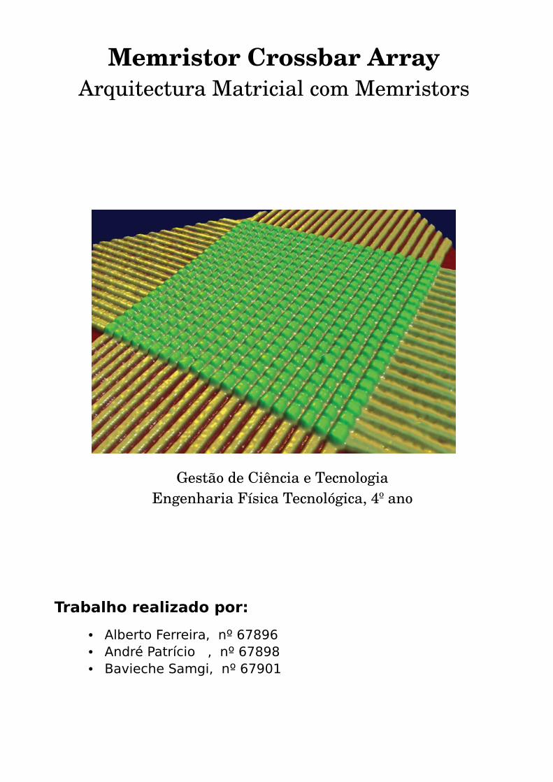
Memristor Crossbar Array Arquitectura Matricial com Memristors Gestão de Ciência e Tecnologia Engenharia Física Tecnológica, 4º ano Trabalho realizado por: • Alberto Ferreira, nº 67896 • André Patrício , nº 67898 • Bavieche Samgi, nº 67901
Transcript of Memristor Crossbar Array - ULisboa · PDF fileMemristor Crossbar Array Arquitectura Matricial...
Memristor Crossbar ArrayArquitectura Matricial com Memristors
Gestão de Ciência e TecnologiaEngenharia Física Tecnológica, 4º ano
Trabalho realizado por:
• Alberto Ferreira, nº 67896• André Patrício , nº 67898 • Bavieche Samgi, nº 67901

1. Identificação do projecto1. Project description ●●●●●●●●●●●●●●●●●●●●●●●●●●●●●●●●●●●●●●●●●●●●●●●●●●●●●●●●●●●●●●●●●●●●●●●●●●●●●●●●●●●●●●●●●●●●●●●●●
Domínio Científico Scientific Domain
Ciências Exactas e da Engenharia
Área científica principalMain Area
Ciências e Engenharia de Materiais
Área científica SecundáriaSecondary area
Nanomateriais e Dispositivos
AcrónimoAcronymMeCrA (Memristor Crossbar Array)
Título do projeto (em português)Project title (in portuguese)Arquitectura Matricial com Memristors
Título do projeto (em inglês)Project title (in english)Memristor Crossbar Array
Financiamento solicitadoRequested funding172.815,60€
Palavra-chave 1 Keyword 1Memristor Memristor
Palavra-chave 2 Keyword 2a
contaminação na arquitectura crossbar array contaminationcrossbar
Palavra-chave 3 Keyword 3integração híbrida hybrid integration
Palavra-chave 4 Keyword 4RAM resistiva (RRAM) Resistive RAM (RRAM)
Data de início do projetoStarting date01-01-2014
Duração do projeto em mesesDuration in months36

2. Instituições envolvidas2. Institutions and their roles ●●●●●●●●●●●●●●●●●●●●●●●●●●●●●●●●●●●●●●●●●●●●●●●●●●●●●●●●●●●●●●●●●●●●●●●●●●●●●●●●●●●●●●●●●●●●●●●●●●●●●
Instituição ProponentePrincipal Contractor
Instituto de Engenharia de Sistemas e Computadores - Microsistemas e Nanotecnologias (INESC MN/INESC/IST/UTL)
Rua Alves Redol, 91000-029, Lisboa,Portugal
Descrição da InstituiçãoPrincipal Contractor Description
INESC Microsistemas e Nanotecnologias (INESC MN) is a private, non-profit R&D institute created in January 2002. INESC MN operates a 250 m2 cleanroom and ajoint 250m2 grey area for magnetic recording head and MR sensor fabrication, biosensor and lab-on-chip fabrication including microfluidics and, being of the greatest interest for our project, thin film semiconductor device and MEMS processing.
INESC MN is dedicated to:
• leading edge R&D in technological areas of micro and nanotechnologies and the application of these technologies to electronic, biological and biomedical devices
• advanced training of young scientists and engineers in micro and nanotechnologies
• transfer of technology to both Portuguese and international industries through collaborative research, contract research, prototyping and consulting
Research Areas
INESC MN main research areas are:• Thin Film MEMS• magnetics• Organic Electronics• Biosensor and Biomedical Applications• Simulation of Materials
Instituição ParticipanteParticipating Institution
Instituto de Engenharia de Sistemas e Computadores - Microsistemas e Nanotecnologias (INESC MN/INESC/IST/UTL)
Rua Alves Redol, 91000-029, Lisboa,Portugal
Descrição da InstituiçãoParticipating Institution Description
Already described as Principal Contractor
Instituição ParticipanteParticipating Institution
International Iberian Nanotechnology Laboratory (INL)
Avenida Mestre José Veiga, s/n4715-330, Braga, Portugal
Descrição da InstituiçãoParticipating Institution Description
Mission
To advance the frontiers of knowledge in Nanoscience and Nanotechnology, developing and transforming the associated technologies, through research and innovation, human capital development, and collaborative work, for the discovery of new knowledge and the creation of societal value and wealth.
Vision
To develop a world leading Nanoscience and Nanotechnology international community, attracting the best research talent, fostering entrepreneurship in an exciting international context and contributing to general socioeconomic strength based on nanotechnology and to related benefits for member countries.
R&D
INL is an international research organisation in Europe in the field of nanoscience and nanotechnology.INL concentrates on nanotechnology, and considers applications to several other areas, following a truly interdisciplinary approach. The Laboratory seeks to answer to major challenges in:
• nonomedicine• nanotechnology applied to environmental and food control • nanoelectronics • nanomachines and nanomanipulation of molecules
For more information about INL consult the website: http://inl.int/about-inl/what-is-inl
Unidade de InvestigaçãoResearch Unit
Instituto de Engenharia de Sistemas e Computadores - Microsistemas e Nanotecnologias (INESC MN/INESC/IST/UTL)
Rua Alves Redol, 91000-029, Lisboa, Portugal
Unidade de Investigação AdicionalAdditional Research Unit
There are no additional research units
Instituição de AcolhimentoHost InstitutionInstituto de Engenharia de Sistemas e Computadores - Microsistemas e Nanotecnologias (INESC MN/INESC/IST/UTL)
Rua Alves Redol, 91000-029, Lisboa, Portugal
3. Componente Científica3. Scientific Component ●●●●●●●●●●●●●●●●●●●●●●●●●●●●●●●●●●●●●●●●●●●●●●●●●●●●●●●●●●●●●●●●●●●●●●●●●●●●●●●●●●●●●●●●●●●●●●●●●
3.1. Sumário3.1 Abstract
3.1.a Em português3.1.a In Portuguese
O elevado consumo de energia em grandes aplicações computacionais tornam necessário desenvolver capacidades de processamento cada vez mais elevadas. A tecnologia actual, baseada em tecnologia CMOS, tem um consumo de energia bastante elevado para conseguir estas velocidades sem que o material constituinte sofra uma detrioração muito célere ([2]). Por outro lado, as suas dimensões fazem com que as grandes máquinas de computação necessitem ter dimensões consideráveis para se conseguir atingir estas velocidades.
Os memristors ([1]) apresentam-se como elementos capazes de suprir esta necessidade em termos de volume e, principalmente, em termos de consumo de energia. Os memristors são componentes que funcionam como resistências com capacidade de memória, isto é, permitem que sejam armazenados tantos níveis de informação quanto a resolução que dispusermos permitir.
A grande aplicação destas estruturas é a criação de uma rede com os mesmos, de modo a poderem ser controlados e permitirem aumentar as combinações de níveis de memória entre os mesmos ou, por outras palavras, aumentar a capacidade de memória dos sistemas ([9]). A programação destes sistemas consiste na aplicação de corrente eléctrica através dos seus terminais ou então aplicando directamente um campo eléctrico.
O projecto MeCrA tem como objectivo apresentar uma topologia para a matriz de memristors com um grau de contaminação inferior às existentes actualmente. As estruturas actuais utilizam transistores conjuntamente com memristors, o que faz com que o número de ligações necessárias seja elevado e ainda que se tenha um grande volume e consumo de energia.
Até agora todas as atenções têm sido dadas a um aperfeiçoamento da técnica híbrida com CMOS mas a nossa abordagem visa trazer um novo paradigma para a investigação neste campo permitindo que novas formas de redução de gastos de energia sejam concebidas. A ideia de investigação centra-se na criação de uma nova estrutura híbrida de memristors que permita reduzir o volume, consumo de energia e contaminação dos diferentes elementos. O primeiro problema é a criação de modelos para os memristors pois a sistematização destes sistemas é muito precária pelo que o trabalho terá que ser desenvolvido de raíz e, dado que esta etapa é essencial para o sucesso de todo o projecto, será necessária uma análise cuidada com contributos de todo o conhecimento experimental adquirido. Por outro lado, quando estamos a pensar em estruturas

das dimensões que propomos construir temos de ter grande atenção a qualquer impureza, pois o efeito desta não é negligenciável numa análise cuidada do memristor produzido. Por fim, tratando-se de uma topologia de matriz completamente inovadora, grande parte do tempo de investigação numa segunda fase será utilizado a optimizar a configuração que um memristor com junções PN poderá ter. As ideias que pretendemos desenvolver são todas no sentido de conseguir unidades de memristor com junções PN o mais compactas possíveis. O plano de trabalhos tem como propósito a obtenção e caracterização do comportamento dos memristors tanto a nível experimental como teórico. Os estudos anteriores permitem-nos ter grande segurança nos resultados que poderemos obter e na correcta análise dos mesmos([3],[4],[5]).
Este projecto é uma cooperação entre duas instituições de referência na área da nanotecnologia, INL e INESC-MN. As máquinas a utilizar neste projecto estão localizadas ora numa das instituições ora noutra, prmitindo grande intercâmbio entre as instituições tanto a nível de conhecimento como de investigadores. O INL está envolvido em vários campos da nanotecnologia com investigadores de nível internacional e é um dos laboratórios com melhores instalações para a prática de investigação nesta área a nível mundial. O INESC-MN tem grandes capacidades na construção de nanoestruturas e possui já trabalhos publicados na área dos memristors ([6],[7],[8]).
Em suma, pretendemos com este projecto:
• obter uma teoria robusta para os memristors;
• optimizar a construção de memristors;
• apresentar um topologia híbrida para a rede de memristors com menor volume e menor consumo de energia;
• apresentar uma rede de memristors com uma taxa de contaminação reduzida.
3.1.b Em inglês3.1.b In English
The high energy consumption in complex computer applications leads to a need for increasingly high processing capabilities.
Current CMOS-based technology has a too high energy consumption to achieve these speeds without the constituent material undergoing a very rapid deterioration ([2]). Moreover, the dimensions of this technology require complex machines to have considerable dimensions in order to achieve these speeds.
Memristors ([1]) appear as a component capable of covering this need in terms of the volume of the components and, above all, in terms of power consumption. Memristors are components which act as resistors with memory capabilities, i.e., they allow you to store in them so many levels of information as the available resolution allows. The major application of these structures is the creation of a network so that they can be controlled and the levels of combinations amongst them be increased or, in other words, to increase the memory capacity of the systems ([9]). We defend that the memristor should be thought of simply as a non-

volatile passive programmable resistor which is programmed by passing current throught it or by applying an electric field at it's terminals.
MeCrA aims to present a topology for the memristors array with a degree of contamination below the currently existing. The current structures use transistors in conjunction with memristors, which causes a big increase in wire connections, in the volume and in the energy consumption. This implementation is based on the new hybrid model for the memristors that the research team aims to develop, which will make possible to achieve a communication system amongst the memristors with a reduced power consumption. Until now all attention has been given to an improvement of the hybrid technique with CMOS but this new approach aims to bring up a new paradigm for research in this field so that new ways to reduce the energy costs are designed.
The first problem with which we are faced in this project is the creation of the models of a memristor because the systematization of these systems is very precarious, so that the work will have to be done from the beginning and given that this step is crucial for the success of the whole project a careful analysis with contribution from all the acquired experimental knowledge will be necessary. Moreover, when we think about structures with the dimensions that we are proposing to build, we must pay great attention to any impurity, because the effect of this imperfection is not negligible in a careful analysis of the memristor produced.
Finally, as it is a completely new innovative topology much of the research time in the second step will be used to optimize the configuration of a memristor with PN junctions. The ideas we intend to develop are all directed towards achieving “memristor + PN junctions” units as compact as possible.
The work plan has as purposes to obtain and characterize the behaviour of the memristors both experimentally and theoretically. Previous studies allow us to have a high degree of confidence on the results we may get and in their correct analysis ([3], [4], [5]).This project is a cooperation between two leading institutions in the field of nanotechnology, INL and INESC-MN.Currently the big machines for use in this project are located either in one institution or in the other, which allows a great exchange between institutions of both knowledge and researchers.
INL is involved in various fields of research in nanotechnology with internationally renowned researchers and it is one of laboratories with best facilities for the practice of research in this area worldwide.INESC-MN has great capabilities in building nanostructures and has already several papers published in the area of memristors ([6],[7],[8]).
Summarizing, with this project we intend to:
• obtain a firm theoretical description of memristors;• optimize the construction of the memristors;• develop a hybrid topology for the memristors array with the lowest
volume and energy comsumption;• develop a memristor's array with reduced contamination rate.
3.2. Descrição Técnica3.2 Technical Description
3.2.1. Revisão da Literatura3.2.1. Literature Review
The discovery of the memristor represented a fundamental change to electronics of an importance no smaller than that of the transistor and it's presence will become indelible in the anals of electronics in the next few decades. Known as the fourth passive circuit element, akin to resistors, capacitors and inductors, it's name derives from memory-resistor and it is a two-terminal electronic component that has it's variable resistance value controlled by the electric flux. Predicted by Leon Chua in 1971 [10] and first discovered in 2008 [1], it's still controversial if the component obeys the definition of a memristor, though certainly has the desired properties.
We defend that the memristor should be thought of simply as a non-volatile passive programmable resistor which is programmed by passing current through it or by applying an electric field at it's terminals. If both of these quantities are null then the memristor maintains it's resistance which can be thought of it's internal memory state in which we're interested.Also, the memristor memory state represents a continuous value instead of a discrete quantity which means that it is naturally capable of representing continuous data or several bits of discrete information, being limited only by the precision of it's reading. This fact alone makes it unmatchable by current standards in electronic-circuit design. It simultaneously allows for the resurgence of the powerful analogue computing now that analogue memory is available and for the development of digital technologies.We explain this point of view and memristor phenomena such as soft and hard-switching in our 2012 report [19].
There are several memristor types: Titanium dioxide, Polymeric – which excel on neuron behaviour replication, ferroelectric, spintronic, Spin-transfer torque magnetoresistances of which we are the leaders worldwide in research [17] and spin memrisistive systems which explore the same concept. We will focus the research on the first class which we want to improve and study with alternative oxides since it was already applied in crossbar architectures.
A single memristor can replace very complex chains of active elements and it's applications are immense, from conventional electronics with summing AmpOp topologies that have application from ADC and DAC converters, to Ultra-Wide-Band signal amplification, to military uses since they are by nature radiation-tolerant, to high-tech computer technology appliable from the smallest devices to the biggest supercomputers and as non-volatile fast data-storage capable of competing with both the highest-density (hard-drives) and the fastest (Flash in SSD's) non-volatile memories whilst running at speeds comparable of those so-called volatile memories like SRAM at very low power consumptions [19]. This will enable computers that boot instantaneously and have only one memory. Beyond storage, memristors allow computation and logic [15] to coexist in the same functional cell, akin to biologic brains, which is much more efficient since more time is spent on computation instead of communication [18]. Recent numbers show in computationally intense workloads performance improvements
in the orders of tens of thousands and so CMOS chips and memristors will eventually have no choice but to be merged, as is being studied for ARM processors today. Another use is mimicking the human brain, having discrete massively-parallel hardware-based artificial-neural-networks (ANN) which can help solve modern complex problems such as adaptive data processing and pattern recognition.
The commonplace architecture in which massive amounts of memristors are packed nowadays is called crossbar array [12]. Stanley Williams and his associates proved the feasibility of the technology with resounding results and that it is possible to embed this technology in CMOS circuits reducing tenfold the size of an ordinary FPGA die whilst increasing it's performance and clock speed.
The crossbar array is a matricial structure of memristors aligned in a cristalline 2D structure type, whose top terminals are linked by parallel wires running across the whole structure atop and another array of parallel wires linking the bottom terminals but along a perpendicular direction. Currently to activate one memristor the whole set of wires is unplugged through galvanic protections in the external electronic control but this is bulky – the crossbar array occupies only 2% of the chip, the rest is electronics – and is sensitive to undesirable internal feedback current paths which we propose to eliminate.
The memristor behaviour and intrinsic phenomena are already well known [14] and has been modeled with good experimental agreement using the techniques developed by Joglekar and Biolek in 2009 [16] and later studied in different material types [13] with promising results for our research. We propose to add PN junctions to the array itself.
The proposed methodology is better than the current implementation because it solves two problems. In the first place, it reduces internal feedback current loops which provide inaccurate impedance readings according to the states of the remaining memristors along the activated data lines even when all the other wires are unplugged. This problem is solved directly by increasing the base-level impedance. Secondly, it allows to simultaneously read and write several memristors that do not share the same data-lines without unplugging the wires through external electronics which is slower. The nano-scale array size will increase slightly in the vertical direction but the device's size is determined by the 2D surface packing of the memristor grid which is not affected by the proposed change, thus, equivalent circuit-size will dramatically decrease and the controlling hardware will be simpler, thus reducing costs, power consumption and increasing switching speed, critical to compete with other technologies.
3.2.2. Plano e Métodos3.2.2. Plan and Methods
Computational sciences need more and more processing capabilities namely higher frequencies for microprocessor operation. Current technology based on CMOS architecture does not reach these needs because the power consumption is too high and systems with considerable processing speeds occupy too much space for a efficient construction.
As we saw on previous section, memristor discovery allowed to have a breakthrough for this problem. The points referenced previously show that the technology is not fully independent concerning computational systems so the

current investigation concentrates on hybrid configurations which present results that foster future investigations in this area. The most important structure studied until our days is a hybrid structure with CMOS technology.
Regardless of this being the most common hybrid implementation it suffers a internal feedback current that makes rigorous measures of the state saved in memory very difficult. In order to solve this constraint we propose a different hybrid configuration which uses PN junctions instead of CMOS transistors. Our 2D matricial structure will be composed by nodes consisting of a memristor with two PN Junctions like is shown in figure “memArray.png”. This approach allows a more robust impedance measure because we create a higher reference level for impedance. As said in Literature Review we are able to create multiple read/write locations without the need of shutting off another area of our matricial complex.
We are the first research group to propose such a dramatic change in memristor hybrid technology state of the art therefore developing this device will be a completely new engineering challenge. Overcoming the challenges showed previously will lead to a completely new way of thinking in memristor technology because the aura of a array contamination won't be a obstacle. Subsequently, a memristor array as high processing frequency computational system will become a closer reality. Research areas as Neuromorphic systems ([11]), military radiation-tolerant devices will all suffer a huge boost with advances in memristor technology.
Our strategy is to develop a hybrid technology which is able to be more competitive than the CMOS hybrid system. We intend to get a lower volume, simpler transmission configuration, less costs and lower power consumptions. In order to create a competitive technology but also to stimulate future research in this area we will divide our work in three stages:
• memristor development (main task 1);• memristor with two PN junctions development (main task 2);• crossbar array implementation (main task 3).
In the first two main tasks we seek to develop a theoretical model concerning our systems, manufacture the prototypes that are viewed as the most promising and fully characterize the memristors constructed. The last main task will focus on manufacture and experimental analysis.
The model that we will initially use for memristor modelization is a standard memristor which uses a metal-insulator-metal structure, usually with Copper Oxide and Titanium Dioxide junction or a Titanium and Platinum junction. After this model is completely structured and functional we will study different materials that also can be used for a metal-insulator-metal configuration as Alumina and Oxide of Magnesium. We will also study a insulator with several layers of different materials composition. The task leader will be André Patrício. All the studies will have the contribution from Alberto Ferreira, our engineering group leader.
The second part of the first main task is the construction of a memristor prototype using the materials studied and approved by the theoretical group. The process will start with a Ion Beam Deposition which will allow us to create a precise region where the substract is accumulated to form the different layers of materials that compose a memristor. It is followed by a cover of resin which allows a CAD machine to draw over the resin and develop our structure. The next

procedure is the revelation with chemicals that dissolve the used resin. The final two processes for the memristor elaboration are the etching and encapsulating thus permitting the electronic configuration to be applied. The task leader will be Alberto Ferreira.
The last part of this main task is to characterize the prototypes produced so we will study the following aspects :
• reliability: we will study the hysteresis cycle and its degradation;• I-V curve: knowing the I-V curve will give us the power consumption
of the model as well as the overall memristor behaviour;• temperature behaviour - it is important to know the temperature
range so we can use materials that can endure in those conditions;• memory - it is the main purpose of this technology, store data so the
resolution of the system and current response will be studied;• frequency behaviour - every electronic system needs to be tested for
frequency behaviour to seek for capacitive or resistive perturbations;• sensitivity to external conditions: noise is a factor of instability in
physical systems so is important to see how the memristor is affected by externalities and produce a statistical analysis of the results in order to get enough information to improve our models and better understand memristor behaviour.
The innovation that we intend to implement in this area is the memristor with two PN junctions, which will take place on the second year of the project. This is the main task 2 that will be structured in three subtasks - the same ones that were referred in main task one. Then again, we will keep the same task leaders. Unlike the memristor study, this study is basically from scratch and it is the revolutionary idea of the research group thus we will increase the time allocated for this task. A profound correlation whit engineering team will be needed in order to get the desired results.
The final main task is a consequence of the results obtained in year two and is the practical goal of the project: build a memristor array with hybrid PN junction structure. This final year will be mainly used for engineering and experimental work so we can get an array that is as small as predicted, consumes less power than its predecessors and has the lowest contamination ratio ever measured.
This project has highly ambitious aims - but we are also confident that we will be able to prove that memristor hybrid technology is a reliable option against current memristor hybrid technologies.
The partners involved in this project complement each other in both infrastructures and knowledge. INESC-MN has a strong background in the deposition of metal-insulator-metal nanostructures with characteristic thicknesses down to the sub-nm range and on nanofabrication processes of devices. The main tasks within the project then include the deposition and fabrication of metal-insulator-metal structures (Susana Freitas) and of the crossbar configuration. Susana Freitas has extended experience on the fabrication and optimization of nanostructured devices. INL will be responsible for the metal-insulator-metal deposition (by magnetron sputtering) and nano-fabrication processes. The new deposition and lithography equipment available at INL will give a strong momentum towards the successful outcome of the project (local coordinator: Miaoxiang Max Chen).

3.2.3. Tarefas3.2.3. Tasks
Lista de tarefas (9)Task list (9)
Designação da tarefa Data de início Data de fim Duração Pessoas * mêsTask denomination Start date End date Duration Person * monthsMemristor Research 01-01-14 15-04-14 3,5 9,8Descrição da Tarefa e Resultados EsperadosTask description and Expected results
Membros da equipa de investigação nesta tarefaMembers of the research team in this task
In this task we will conduct material research, modelling, simulation and optimization of the memristor.
Several oxide layers will be studied for the memristor stack, as an alternative to the already studied and presently state-of-the-art TiO2 stack-based memristor from HP Labs which we have detected previously as producing too much heat when read which is unacceptable for a low-powered high-density passive device.
However, since enhancing the memory properties of the device is desired, very resistive oxide layers like MgO, TiO2 and TgO will be the object of our research as our previous research shows them to be in some experiments more promising and well-behaved materials in terms of memristive properties that only arise at the nano-scale.
We will model the memristors with our in-house developed stack that is similar to the industry-standard TiO2 stack type but has a thin extra metallic barrier which improves the memristive behaviour. This memristor stack will be modeled for the different studied oxide layers.
We will then simulate the whole memristor behaviour in terms of switching speed, switching balance, voltage and current sensitivity and impurities behaviour through cumulative cycles for the different material oxide layers.
Through geometry the memristor stack will be optimized for each oxide material. The effect of different layers depths, memristor's width and radially symmetric shape affect the memristor behaviour, specifically it's soft and hard-switching behaviour. This is critical in a crossbar array architecture as it's one of the determinant reasons for signal contamination and internal feedback loops. Of course, the stability and consistency of the internal state through cumulative cycles which is determined by the accumulated dispersion of the impurities will have to be optimized too for good reads to be obtained.
Alberto Artilheiro Ferreira; André Morgado Patrício; Bavieche Jamnadas Samgi; Susana Isabel Pinheiro Cardoso de Freitas; Paulo Jorge Peixeiro de Freitas; (BI) Bolseiro de Investigação (Mestre) 1.
Designação da tarefa Data de início Data de fim Duração Pessoas * mêsTask denomination Start date End date Duration Person * monthsKick-off Meeting 02-01-14 02-01-14 0,0 0,0Descrição da Tarefa e Resultados EsperadosTask description and Expected results
Membros da equipa de investigação nesta tarefaMembers of the research team in this task
Official start of the project. This early meeting will have an introductory character and will serve the purpose of discussing possible date issues.
Alberto Artilheiro Ferreira; André Morgado Patrício; Bavieche Jamnadas Samgi; João José Sousa de Alencastre Ornelas Pereira; Miaoxiang Max Chen; Susana Isabel Pinheiro Cardoso de Freitas; Luca Luschi ; Rui Manuel Ferreira Sampaio; Paulo Jorge Peixeiro de Freitas; (BI) Bolseiro de Investigação (Mestre) 1; (BI) Bolseiro de Investigação (Mestre) 2.

Designação da tarefa Data de início Data de fim Duração Pessoas * mêsTask denomination Start date End date Duration Person * monthsConstruction of the memristor 16-04-14 15-08-14 4,2 9,4Descrição da Tarefa e Resultados EsperadosTask description and Expected results
Membros da equipa de investigação nesta tarefaMembers of the research team in this task
We will manufacture only the most promising memristor prototypes.
This task involves using an ion deposition with the IBM machine for the bottom layer, followed by application of the photoresist, lasering the photoresist layer to draw the desired components and then revealing it. In the end, etching is applied. This method is repeated for the different layers. Membros da equipa de investigação nesta tarefa Members of the research team in this task
Alberto Artilheiro Ferreira; João José Sousa de Alencastre Ornelas Pereira; Susana Isabel Pinheiro Cardoso de Freitas; Rui Manuel Ferreira Sampaio;(BI) Bolseiro de Investigação (Mestre) 2.
Designação da tarefa Data de início Data de fim Duração Pessoas * mêsMemristor Characterization 16-08-14 31-12-14 4,7 17,9Descrição da Tarefa e Resultados EsperadosTask description and Expected results
Membros da equipa de investigação nesta tarefa
Members of the research team in this task
In this task the memristor will be characterized in reliability, I-V curve, temperature behaviour and sensitivity to external conditions. Analysis of the results and optimization will be performed.
To test reliability, the memristor will be subjected to several thousands of read/write cycles in a special machine. This device is meant to last at least 10^5 read/write cycles since it is the minimum required for computer storage systems which is as of today one of the major areas of interest of this technology – Resistive RAM (RRAM).
The I-V curve for a memristor must be well characterized since it is the basis for determining it's soft and hard-switching behaviour as well as switching times which implies how it should be written and is also crucial in determining it's internal state (main characteristic of a memristor) which implies how the read-cycle should be defined.
The effect of temperature on the plasticity of the internal state will be studied. This is important to determine the maximum operating temperature of the device, above which the device isn't guaranteed to store it's state for the specified time. The inherent heating of the device in reading and writing operations will be studied to guarantee that low levels of heat are generated which is crucial to operate the device without active cooling thus maintaining the very-low energy consumption which is highly praised in this technology.
The desired property of the memristor is the memory. The hysteresis will be studied more in depth and it's variation after many read/write cycles. How information degrades will be measured. The variation should be regular and very small. This characteristics will have to be documented. Permanency of the different state values when the memristor is subjected to no signals at all will also be measured. From this the memory state duration will be determined.
The sensivity to high frequency signals will be studied. Spikes will be used in a signal generator to probe the memristor behaviour for the high frequencies. The sensitivity should in principle be very low as frequency increases and how low it is is important to know beforehand so that the array can be used in EMF noisy environments. The very low frequency behaviour will also be studied to determine if more precise writes or reads are possible versus the standard read/write operation speeds.
The memristor will also be placed in a noisy EMF environment and subjected to monochromatic and wide-band signals of several frequencies of the EM spectrum and the variation of it's internal state will be measured. Also, it will be placed in a real circuit with one regulated power supply and the influence of pink-noise in the internal state will also be studied.
Statistical analysis of the previous results and comparison with the model results and the final theoric model will be adapted to perfectly reproduce the experimental results.
André Morgado Patrício; Bavieche Jamnadas Samgi; Susana Isabel Pinheiro Cardoso de Freitas; Luca Luschi (BI) Bolseiro de Investigação (Mestre) 1; (BI) Bolseiro de Investigação (Mestre) 2.

Designação da tarefa Data de início Data de fim Duração Pessoas * mêsTwo PN Junctions Memristor Research 01-01-15 30-04-15 4,1 10,8Descrição da Tarefa e Resultados EsperadosTask description and Expected results
Membros da equipa de investigação nesta tarefaMembers of the research team in this task
A model for the memristor combined with the two inversely polarized PN junctions will be produced based on the memristor model obtained from the previous stage. Since memristive properties arise at the nano-scale the PN junctions themselves could be designed to behave memristively though that won't be explored in this work, we'll leave it to later after the concept is proven. Since the problem can no longer be considered to be one-dimensional, microscopical simulations of the device and dopants will have to be used. CUDA programming will be used for this stage to deliver accurate results in reasonable amounts of time.
In this task several geometries will be simulated for the two PN junctions, namely, the parallel prisms placement at the memristor head and the more symmetric internal/external PN junction rings placed also atop the memristor. Beyond the standard properties of the memristor in which we are concerned, we are particularly interested in knowing if the impurities dispersion which control the internal state of the device are better controlled and better distributed in the latter PN junctions form and compare it to the former, since the building process of the latter is pricier.
We will optimize the geometry of the PN junctions to isolate the memristor up to the threshold voltage of 0.6-0.7V. The junctions will be optimized to keep memristivity disruption to a minimum.
André Morgado Patrício; Susana Isabel Pinheiro Cardoso de Freitas; Paulo Jorge Peixeiro de Freitas; (BI) Bolseiro de Investigação (Mestre) 1.
Designação da tarefa Data de início Data de fim Duração Pessoas * mêsCharacterization of the device 01-09-15 29-02-16 6,2 29,1Descrição da Tarefa e Resultados EsperadosTask description and Expected results
Membros da equipa de investigação nesta tarefaMembers of the research team in this task
In this task the same techniques and metrics will be used as in the characterization of the memristor task. The difference is that the I-V curves will produce resistive behaviours up to the threshold tension of the PN junctions and then memristive behaviours onward. The activation tension will supposedly be above 0.7V.
André Morgado Patrício; Bavieche Jamnadas Samgi; Susana Isabel Pinheiro Cardoso de Freitas; Luca Luschi ;(BI) Bolseiro de Investigação (Mestre) 2;(BI) Bolseiro de Investigação (Mestre) 1; (BI) Bolseiro de Investigação (Lincenciado/Bacharel).
Designação da tarefa Data de início Data de fim Duração Pessoas * mêsBuilding the two PN Junctions Device 01-05-15 31-08-15 4,1 12,6Descrição da Tarefa e Resultados EsperadosTask description and Expected results
Membros da equipa de investigação nesta tarefaMembers of the research team in this task
We will manufacture only the most promising memristor prototypes and optimize the PN junctions construction.
The same fabrication techniques used to build the memristor will be used to build the memristor with two PN junctions. After building the standard memristor a layer is created and with etching the excesses are removed and the first PN junction is created, then the second, in the same way.
Alberto Artilheiro Ferreira; João José Sousa de Alencastre Ornelas Pereira; Rui Manuel Ferreira Sampaio; Miaoxiang Max Chen;(BI) Bolseiro de Investigação (Mestre) 2.
Designação da tarefa Data de início Data de fim Duração Pessoas * mêsCharacterization of the device 01-09-15 29-02-16 6,2 29,1Descrição da Tarefa e Resultados EsperadosTask description and Expected results
Membros da equipa de investigação nesta tarefaMembers of the research team in this task
In this task the same techniques and metrics will be used as in the characterization of the memristor task. The difference is that the I-V curves will produce resistive behaviours up to the threshold tension of the PN junctions and then memristive behaviours onward. The activation tension will supposedly be above 0.7V.
André Morgado Patrício; Bavieche Jamnadas Samgi; Susana Isabel Pinheiro Cardoso de Freitas; Luca Luschi ;(BI) Bolseiro de Investigação (Mestre) 2;(BI) Bolseiro de Investigação (Mestre) 1; (BI) Bolseiro de Investigação (Lincenciado/Bacharel).

Designação da tarefa Data de início Data de fim Duração Pessoas * mêsArray construction 01-03-16 31-07-16 5,2 25,2Descrição da Tarefa e Resultados EsperadosTask description and Expected results
Membros da equipa de investigação nesta tarefaMembers of the research team in this task
Both the standard and the proposed arrays share the same construction type, except for the middle layer which is in the first case composed by memristors and in the latter by the memristors with the associated PN junctions. First, the bottom layer is deposited and through photoresist, lasering revealing and etching it is possible to produce the bottom layer with the desired parallel wire lines, then the memristor is built on top and the procedure is repeated on the top layer to generate the other set of parallel wires.
Alberto Artilheiro Ferreira; João José Sousa de Alencastre Ornelas Pereira; Susana Isabel Pinheiro Cardoso de Freitas; Rui Manuel Ferreira Sampaio;(BI) Bolseiro de Investigação (Mestre) 2;(BI) Bolseiro de Investigação (Lincenciado/Bacharel)..
Designação da tarefa Data de início Data de fim Duração Pessoas * mêsArray characterization 01-08-16 31-12-16 5,2 12,4Descrição da Tarefa e Resultados EsperadosTask description and Expected results
Membros da equipa de investigação nesta tarefa
Members of the research team in this task
In this study we measure the properties of both arrays, specifically the inter-memristor reading contamination on the same data-lines, as well as in independent data-lines. We then calculate the dB-attenuation for contamination of devices in the same data-line of our specialized array versus the standard array, as well as produce the final device characterization with all the parameters studied in the memristor and the two PN junctions memristor phase.
Bavieche Jamnadas Samgi; Susana Isabel Pinheiro Cardoso de Freitas; Luca Luschi ;(BI) Bolseiro de Investigação (Mestre) 2; (BI) Bolseiro de Investigação (Lincenciado/Bacharel).

3.2.4. Calendarização e Gestão do Projeto3.2.4. Project Timeline and Management
3.2.4.a Descrição da Estrutura de Gestão3.2.4.a Description of the Management Structure
Given that we have just two partner groups, the best suited management structure to realize the innovation potential of MeCrA is one with short lines of communication and straightforward decision making. We'll have an executive board (EB) represented by the project coordinator, the task leaders and the local project coordinators. The EB will be chaired by the project coordinator and will supervise the execution of the project and take actions and decisions accordingly. Local coordinators in collaboration with the task leaders will be responsible for daily management activities.
Coordination
INESC MN, as the coordinator, will be the intermediary between the two partner groups and FCT. As such, INESC MN will be responsible for performing all the tasks assigned in the Project Agreement, which include:
• supervision of the project partners compliance to their obligations;• collection, review and submittal of report and other deliverables to FCT;• preparation of agendas for EB meetings and chairing them if relevant;• providing consumables needed for the specific work to be done
at INL, using their facilities at zero bench fees;• administration of the FCT financial contribution and other obligations
forthcoming of the Project Agreement.
Executive board
The EB will be made up by the project coordinator, task leaders and local project coordinators. The EB will be mainly responsible for high quality preparation and execution of the project. As such we will meet at least three times per task. The purpose of these meetings is to collect information on the project progress in order to assess the compliance of the project and monitor its overall progress. During these meetings, each partner is asked to report on results achieved and the task leader will report on the task progress and develop a future work plan.
Although it is preferable to have unanimous decisions, all decisions will be made based on a two-thirds majority. Responsabilities of the EB members will include:
• monitorize the progress of the project (scientifically and financially);• support coordination and preparation of deliverables and related items;• agree on the date for publications, reports and intellectual property.
Task leaders
Each task leader assumes responsability for the compliance and progress of the tasks and also for the timely delivery of reports and other deliverables to the EB.
The team allocated to each task will meet on a weekly basis to assess the work done. The task leaders will report directly to the EB for proposing changes to a task, alerting to a delay and making decisions on task and budget exchange when such action affects only the scope of the given task.
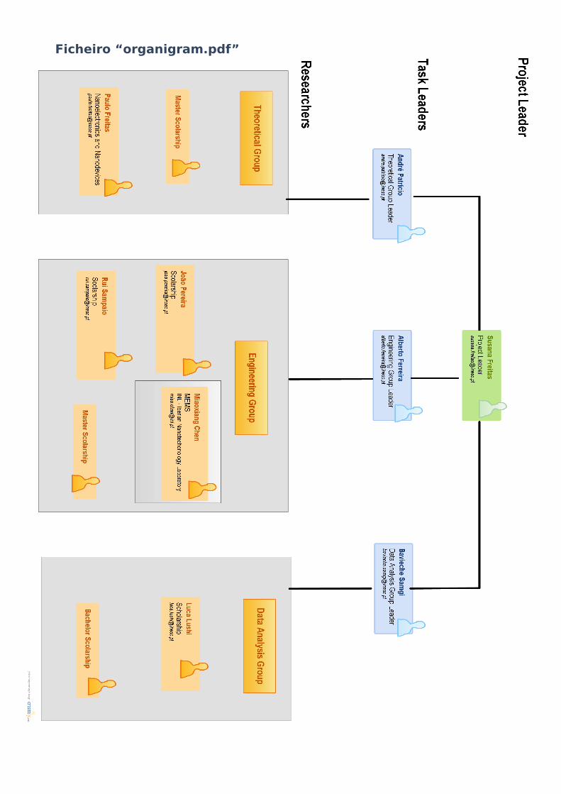
An organigram of the management structure is presented in file “organigram.pdf” at 9. Attachments (if exists).

3.2.4.b Lista de Milestones3.2.4.b Milestone List
3.2.4.c Cronograma3.2.4.c Timeline
Ficheiro com a designação "ganttChart.pdf", no 9. Ficheiros Anexos, desta Visão Global (caso exista).File with the name "ganttChart.pdf" at 9. Attachments (if exists).
Data Designação da milestoneDate Milestone denomination
15-04-14 M1 List of the most promising materials
DescriçãoDescription
Data Designação da milestone
Date Milestone denomination
15-08-14 M2 Functional Memristor ready for testingDescrição
Description
Data Designação da milestone
Date Milestone denomination
31-12-14 M4 Systematization of memristor properties
Descrição
Description
We intend to create a full description of the produced memristors
Data Designação da milestone
Date Milestone denomination
31-08-15 M3 Functional Memristor with PN junction ready for testing
Descrição
Description
Data Designação da milestoneDate Milestone denomination
31-07-16 M5 Memristor Crossbar Array BuiltDescriçãoDescription
Data Designação da milestoneDate Milestone denomination
31-12-16 M6 Final Report
DescriçãoDescription
The milestone comprises the conclusion of the memristor simulation and optimization. Materials with best simulation results are ready for implementation.
A functional memristor is built and all the infrastructure to test all features relevant for this implementation.
Memristor with PN junction implementation fully prepared for testing. All support for testing is prepared.
Several Memristor Crossbar Array units built and all equipment necessary for testing is loaded.
Final report is delivered and two international papers are generated from the final report.
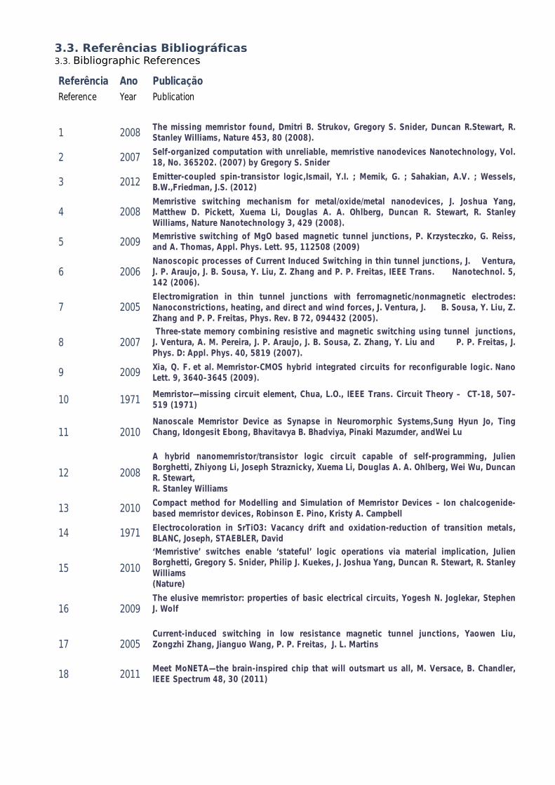
3.3. Referências Bibliográficas3.3. Bibliographic References
Referência Ano PublicaçãoReference Year Publication
1 2008
2 2007
3 2012
4 2008
5 2009
6 2006
7 2005
8 2007
9 2009
10 1971
11 2010
12 2008
13 2010
14 1971
15 2010
16 2009
17 2005
18 2011
The missing memristor found, Dmitri B. Strukov, Gregory S. Snider, Duncan R.Stewart, R. Stanley Williams, Nature 453, 80 (2008).
Self-organized computation with unreliable, memristive nanodevices Nanotechnology, Vol. 18, No. 365202. (2007) by Gregory S. Snider
Emitter-coupled spin-transistor logic,Ismail, Y.I. ; Memik, G. ; Sahakian, A.V. ; Wessels, B.W.,Friedman, J.S. (2012)
Memristive switching mechanism for metal/oxide/metal nanodevices, J. Joshua Yang, Matthew D. Pickett, Xuema Li, Douglas A. A. Ohlberg, Duncan R. Stewart, R. Stanley Williams, Nature Nanotechnology 3, 429 (2008).
Memristive switching of MgO based magnetic tunnel junctions, P. Krzysteczko, G. Reiss, and A. Thomas, Appl. Phys. Lett. 95, 112508 (2009)
Nanoscopic processes of Current Induced Switching in thin tunnel junctions, J. Ventura, J. P. Araujo, J. B. Sousa, Y. Liu, Z. Zhang and P. P. Freitas, IEEE Trans. Nanotechnol. 5, 142 (2006).
Electromigration in thin tunnel junctions with ferromagnetic/nonmagnetic electrodes: Nanoconstrictions, heating, and direct and wind forces, J. Ventura, J. B. Sousa, Y. Liu, Z. Zhang and P. P. Freitas, Phys. Rev. B 72, 094432 (2005).
Three-state memory combining resistive and magnetic switching using tunnel junctions, J. Ventura, A. M. Pereira, J. P. Araujo, J. B. Sousa, Z. Zhang, Y. Liu and P. P. Freitas, J. Phys. D: Appl. Phys. 40, 5819 (2007).
Xia, Q. F. et al. Memristor-CMOS hybrid integrated circuits for reconfigurable logic. Nano Lett. 9, 3640–3645 (2009).
Memristor—missing circuit element, Chua, L.O., IEEE Trans. Circuit Theory – CT-18, 507–519 (1971)
Nanoscale Memristor Device as Synapse in Neuromorphic Systems,Sung Hyun Jo, Ting Chang, Idongesit Ebong, Bhavitavya B. Bhadviya, Pinaki Mazumder, andWei Lu
A hybrid nanomemristor/transistor logic circuit capable of self-programming, Julien Borghetti, Zhiyong Li, Joseph Straznicky, Xuema Li, Douglas A. A. Ohlberg, Wei Wu, Duncan R. Stewart,R. Stanley Williams
Compact method for Modelling and Simulation of Memristor Devices – Ion chalcogenide-based memristor devices, Robinson E. Pino, Kristy A. Campbell
Electrocoloration in SrTiO3: Vacancy drift and oxidation-reduction of transition metals, BLANC, Joseph, STAEBLER, David
‘Memristive’ switches enable ‘stateful’ logic operations via material implication, Julien Borghetti, Gregory S. Snider, Philip J. Kuekes, J. Joshua Yang, Duncan R. Stewart, R. Stanley Williams(Nature)
The elusive memristor: properties of basic electrical circuits, Yogesh N. Joglekar, Stephen J. Wolf
Current-induced switching in low resistance magnetic tunnel junctions, Yaowen Liu, Zongzhi Zhang, Jianguo Wang, P. P. Freitas, J. L. Martins
Meet MoNETA—the brain-inspired chip that will outsmart us all, M. Versace, B. Chandler, IEEE Spectrum 48, 30 (2011)
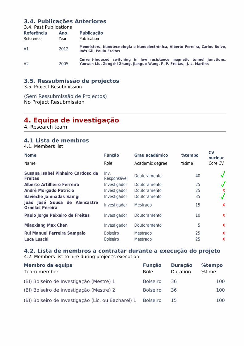
3.4. Publicações Anteriores3.4. Past Publications
3.5. Ressubmissão de projectos3.5. Project Resubmission
(Sem Ressubmissão de Projectos)No Project Resubmission
4. Equipa de investigação4. Research team
4.1 Lista de membros4.1. Members list
1
4.2. Lista de membros a contratar durante a execução do projeto4.2. Members list to hire during project's execution
Referência Ano PublicaçãoReference Year Publication
A1 2012
A2 2005
Memristors, Nanotecnologia e Nanoelectrónica, Alberto Ferreira, Carlos Ruivo, Inês Gil, Paulo Freitas
Current-induced switching in low resistance magnetic tunnel junctions, Yaowen Liu, Zongzhi Zhang, Jianguo Wang, P. P. Freitas, J. L. Martins
Membro da equipa Função Duração %tempoTeam member Role Duration %time
(BI) Bolseiro de Investigação (Mestre) 1 Bolseiro 36 100
(BI) Bolseiro de Investigação (Mestre) 2 Bolseiro 36 100
(BI) Bolseiro de Investigação (Lic. ou Bacharel) 1 Bolseiro 15 100
Nome Função Grau académico %tempo
Role Core CV
Doutoramento 40
Alberto Artilheiro Ferreira Investigador Doutoramento 25André Morgado Patrício Investigador Doutoramento 25 X
Investigador Doutoramento 35
Investigador Mestrado 15 X
Investigador Doutoramento 10 X
Investigador Doutoramento 5 X
Rui Manuel Ferreira Sampaio Bolseiro Mestrado 25 X
Bolseiro Mestrado 25 X
CV nuclear
Name Academic degree %time
Susana Isabel Pinheiro Cardoso de Freitas
Inv. Responsável
Bavieche Jamnadas SamgiJoão José Sousa de Alencastre Ornelas Pereira
Paulo Jorge Peixeiro de Freitas
Miaoxiang Max Chen
Luca Luschi

5. Outros projetos5. Other projects●●●●●●●●●●●●●●●●●●●●●●●●●●●●●●●●●●●●●●●●●●●●●●●●●●●●●●●●●●●●●●●●●●●●●●●●●●●●●●●●●●●●●●●●●●●●●●●●●
5.1. Projetos financiados5.1. Funded projects
(Sem Projectos Financiados)No Funded Projects
5.2. Candidaturas similares5.2. Similar applications
(Sem Candidaturas Similares)(No Similar applications)
6. Indicadores previstos6. Expected indicators ●●●●●●●●●●●●●●●●●●●●●●●●●●●●●●●●●●●●●●●●●●●●●●●●●●●●●●●●●●●●●●●●●●●●●●●●●●●●●●●●●●●●●●●●●●●●●●●●●●●●●
Indicadores de realização previstos para o projetoExpected output indicatorsDescrição
2014 2015 2016 TotalDescriptionA - PublicaçõesPublicationsLivros
0 0 0 0BooksArtigos em revistas internacionais
3 5 7 15Papers in international journalsArtigos em revistas nacionais
0 0 1 1Papers in national journalsB - ComunicaçõesCommunicationsComunicações em encontros científicos internacionais
2 4 4 10Communications in international meetingsComunicações em encontros científicos nacionais
0 1 1 2Communications in national meetingsC - Relatórios
1 1 1 3ReportsD - Organização de seminários e conferências
0 1 1 2Organization of seminars and conferencesE - Formação avançadaAdvanced trainingTeses de Doutoramento
0 0 2 2PhD thesesTeses de Mestrado
0 0 1 1Master thesesOutras
0 0 0 0OthersF - Modelos
0 1 1 2ModelsG - Aplicações computacionais
0 0 0 0SoftwareH - Instalações piloto
0 0 0 0Pilot plantsI - Protótipos laboratoriais
0 0 0 0PrototypesJ - Patentes
0 1 1 2Patents
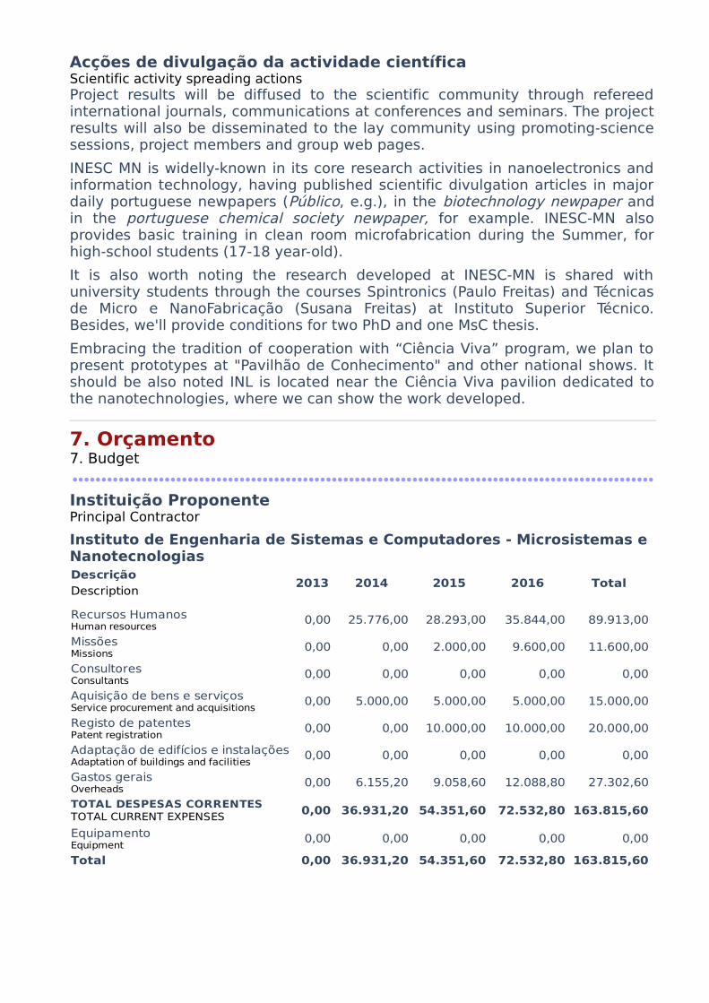
Acções de divulgação da actividade científicaScientific activity spreading actionsProject results will be diffused to the scientific community through refereed international journals, communications at conferences and seminars. The project results will also be disseminated to the lay community using promoting-science sessions, project members and group web pages.
INESC MN is widelly-known in its core research activities in nanoelectronics and information technology, having published scientific divulgation articles in major daily portuguese newpapers (Público, e.g.), in the biotechnology newpaper and in the portuguese chemical society newpaper, for example. INESC-MN also provides basic training in clean room microfabrication during the Summer, for high-school students (17-18 year-old).
It is also worth noting the research developed at INESC-MN is shared with university students through the courses Spintronics (Paulo Freitas) and Técnicas de Micro e NanoFabricação (Susana Freitas) at Instituto Superior Técnico. Besides, we'll provide conditions for two PhD and one MsC thesis.
Embracing the tradition of cooperation with “Ciência Viva” program, we plan to present prototypes at "Pavilhão de Conhecimento" and other national shows. It should be also noted INL is located near the Ciência Viva pavilion dedicated to the nanotechnologies, where we can show the work developed.
7. Orçamento7. Budget ●●●●●●●●●●●●●●●●●●●●●●●●●●●●●●●●●●●●●●●●●●●●●●●●●●●●●●●●●●●●●●●●●●●●●●●●●●●●●●●●●●●●●●●●●●●●●●●●●●●●●
Instituição ProponentePrincipal Contractor
Instituto de Engenharia de Sistemas e Computadores - Microsistemas e NanotecnologiasDescrição
2013 2014 2015 2016 Total
0,00 25.776,00 28.293,00 35.844,00 89.913,00
0,00 0,00 2.000,00 9.600,00 11.600,00
0,00 0,00 0,00 0,00 0,00
0,00 5.000,00 5.000,00 5.000,00 15.000,00
0,00 0,00 10.000,00 10.000,00 20.000,00
0,00 0,00 0,00 0,00 0,00
0,00 6.155,20 9.058,60 12.088,80 27.302,60
0,00 36.931,20 54.351,60 72.532,80 163.815,60
0,00 0,00 0,00 0,00 0,00
Total 0,00 36.931,20 54.351,60 72.532,80 163.815,60
Description
Recursos HumanosHuman resources
MissõesMissions
ConsultoresConsultants
Aquisição de bens e serviçosService procurement and acquisitions
Registo de patentesPatent registration
Adaptação de edifícios e instalaçõesAdaptation of buildings and facilities
Gastos geraisOverheads
TOTAL DESPESAS CORRENTESTOTAL CURRENT EXPENSES
EquipamentoEquipment
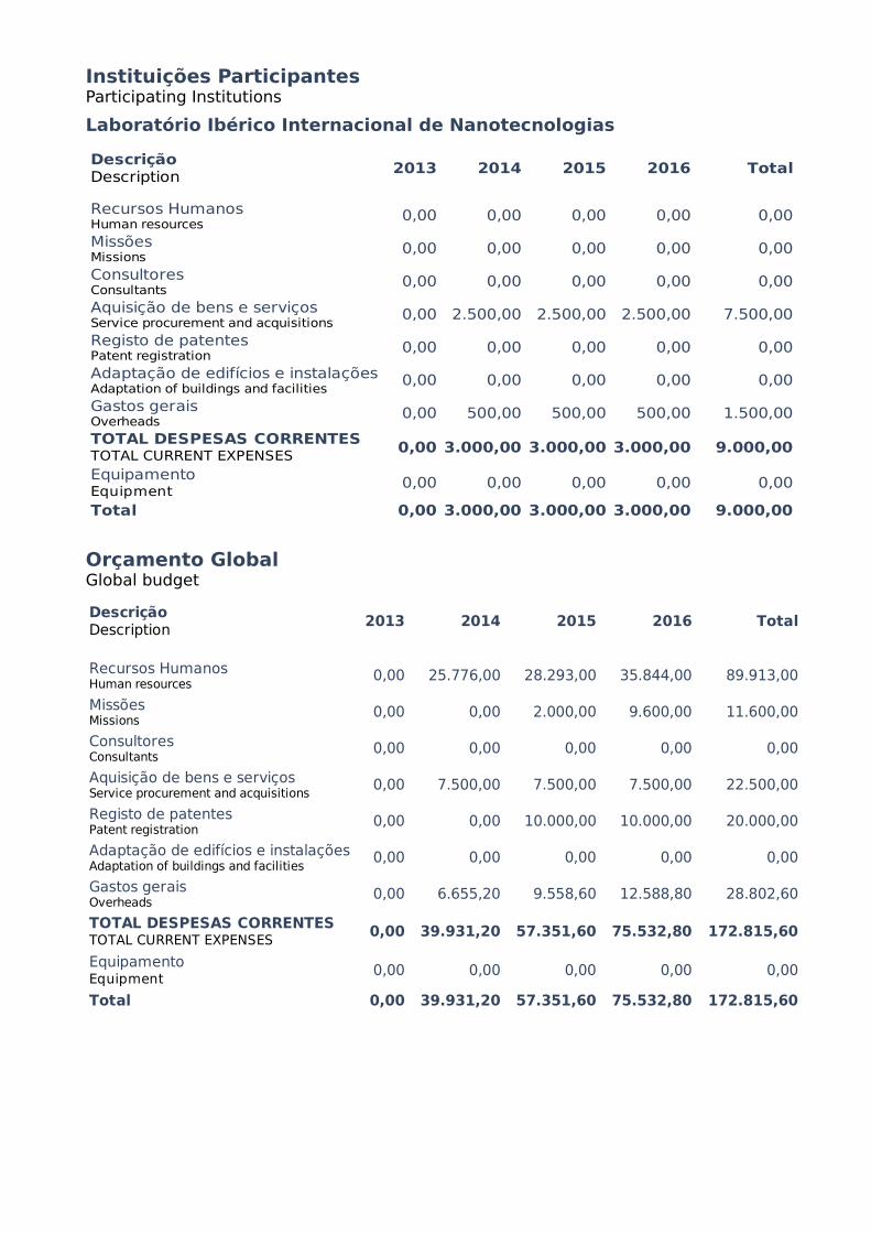
Instituições ParticipantesParticipating Institutions
Laboratório Ibérico Internacional de Nanotecnologias
Orçamento GlobalGlobal budget
2013 2014 2015 2016 Total
0,00 0,00 0,00 0,00 0,00
0,00 0,00 0,00 0,00 0,00
0,00 0,00 0,00 0,00 0,00
0,00 2.500,00 2.500,00 2.500,00 7.500,00
0,00 0,00 0,00 0,00 0,00
0,00 0,00 0,00 0,00 0,00
0,00 500,00 500,00 500,00 1.500,00
0,00 3.000,00 3.000,00 3.000,00 9.000,00
0,00 0,00 0,00 0,00 0,00
Total 0,00 3.000,00 3.000,00 3.000,00 9.000,00
DescriçãoDescription
Recursos HumanosHuman resources
MissõesMissions
ConsultoresConsultants
Aquisição de bens e serviçosService procurement and acquisitions
Registo de patentesPatent registration
Adaptação de edifícios e instalaçõesAdaptation of buildings and facilities
Gastos geraisOverheads
TOTAL DESPESAS CORRENTESTOTAL CURRENT EXPENSESEquipamentoEquipment
2013 2014 2015 2016 Total
0,00 25.776,00 28.293,00 35.844,00 89.913,00
0,00 0,00 2.000,00 9.600,00 11.600,00
0,00 0,00 0,00 0,00 0,00
0,00 7.500,00 7.500,00 7.500,00 22.500,00
0,00 0,00 10.000,00 10.000,00 20.000,00
0,00 0,00 0,00 0,00 0,00
0,00 6.655,20 9.558,60 12.588,80 28.802,60
0,00 39.931,20 57.351,60 75.532,80 172.815,60
0,00 0,00 0,00 0,00 0,00
Total 0,00 39.931,20 57.351,60 75.532,80 172.815,60
DescriçãoDescription
Recursos HumanosHuman resources
MissõesMissions
ConsultoresConsultants
Aquisição de bens e serviçosService procurement and acquisitions
Registo de patentesPatent registration
Adaptação de edifícios e instalaçõesAdaptation of buildings and facilities
Gastos geraisOverheads
TOTAL DESPESAS CORRENTESTOTAL CURRENT EXPENSES
EquipamentoEquipment
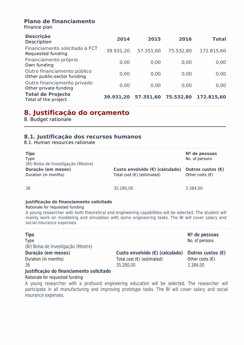
Plano de financiamentoFinance plan
8. Justificação do orçamento8. Budget rationale
8.1. Justificação dos recursos humanos8.1. Human resources rationale
2014 2015 2016 Total
39.931,20 57.351,60 75.532,80 172.815,60
0,00 0,00 0,00 0,00
0,00 0,00 0,00 0,00
0,00 0,00 0,00 0,00
39.931,20 57.351,60 75.532,80 172.815,60
DescriçãoDescriptionFinanciamento solicitado à FCTRequested funding
Financiamento próprioOwn funding
Outro financiamento públicoOther public-sector funding
Outro financiamento privadoOther private funding
Total do ProjectoTotal of the project
Tipo Nº de pessoasType No. of persons(BI) Bolsa de Investigação (Mestre)Duração (em meses) Custo envolvido (€) (calculado) Outros custos (€)Duration (in months) Other costs (€)36 35.280,00 3.384,00Justificação do financiamento solicitadoRationale for requested funding
Total cost (€) (estimated)
A young researcher with a profound engineering education will be selected. The researcher will participate in all manufacturing and improving prototype tasks. The BI will cover salary and social insurance expenses.
Tipo Nº de pessoasType No. of persons(BI) Bolsa de Investigação (Mestre)Duração (em meses) Custo envolvido (€) (calculado) Outros custos (€)Duration (in months) Other costs (€)
36 35.280,00 3.384,00
Justificação do financiamento solicitadoRationale for requested funding
Total cost (€) (estimated)
A young researcher with both theoretical and engineering capabilities will be selected. The student will mainly work on moddeling and simulation with some engineering tasks. The BI will cover salary and social insurance expenses.

●●●●●●●●●●●●●●●●●●●●●●●●●●●●●●●●●●●●●●●●●●●●●●●●●●●●●●●●●●●●●●●●●●●●●●●●●●●●●●●●●●●●●●●●●●●●●●●●●●●●●
8.2. Justificação de missões8.2. Missions rationale
8.3. Justificação de consultores8.3. Consultants rationale
(Vazio)(Void)
Tipo Nº de pessoasType No. of persons(BI) Bolsa de Investigação (Lic. Ou Bacharel)Duração (em meses) Custo envolvido (€) (calculado) Outros custos (€)Duration (in months) Other costs (€)15 11.175,00 1.410,00Justificação do financiamento solicitadoRationale for requested funding
Total cost (€) (estimated)
A young researcher with good experimental physics skills will be selected. The student will mainly work on testing and data analysis. with some engineering tasks. The BI will cover salary and social insurance expenses.
Tipo Nº de deslocaçõesType No. of participationsInternational Meeting 2Local Custo envolvido (€)Venue Cost (€)
Boston, USA 4.400,00Justificação do financiamento solicitadoRationale for requested funding
First International presentation of memristor with PN junctions
Tipo
2Local Custo envolvido (€)
Xangai, China 5.200,00Justificação do financiamento solicitado
Nº de deslocaçõesType No. of participationsInternational Meeting
Venue Cost (€)
Rationale for requested funding
Final results will be presented and international feedback is expected
Tipo Nº de deslocaçõesType No. of participationsNational Meeting 3Local Custo envolvido (€)Venue Cost (€)Braga, Portugal 2.000,00Justificação do financiamento solicitadoRationale for requested funding
Memristor investigation and results presented but also memristor with PN junctions mechanism

8.4. Justificação de aquisição de bens e serviços8.4. Service procurement and acquisitions
Tipo Custo (€)Type Cost (€)
Consumables for the diverse applications needed for this project. 15.000,00
Justificação do financiamento solicitadoRationale for requested funding
Our project will encompass several nanotechnology processes. A process like lithography need hundreds of masks. Besides we need to purchase several wafers to operate many of our building tasks. We will also require lens (characterization and manufacturing), solvents, resins. Cleanroom maintenance is considered, too.
Tipo Custo (€)
7.500,00Justificação do financiamento solicitado
Type Cost (€)Consumables for the diverse applications needed for this project.
Rationale for requested fundingThe requested amount will be spent mainly on Cleanroom maintenance, masks and wafers.
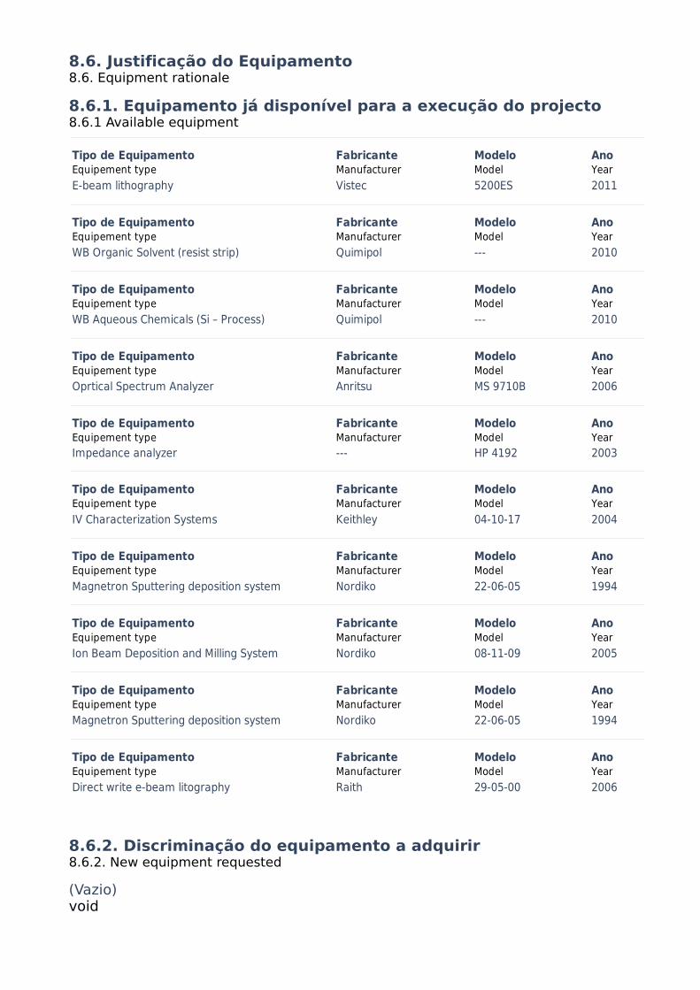
8.6. Justificação do Equipamento8.6. Equipment rationale
8.6.1. Equipamento já disponível para a execução do projecto8.6.1 Available equipment
8.6.2. Discriminação do equipamento a adquirir8.6.2. New equipment requested
(Vazio)void
Tipo de Equipamento Fabricante Modelo AnoEquipement type Manufacturer Model Year
E-beam lithography Vistec 5200ES 2011
Tipo de Equipamento Fabricante Modelo AnoEquipement type Manufacturer Model Year
WB Organic Solvent (resist strip) Quimipol --- 2010
Tipo de Equipamento Fabricante Modelo AnoEquipement type Manufacturer Model Year
WB Aqueous Chemicals (Si – Process) Quimipol --- 2010
Tipo de Equipamento Fabricante Modelo AnoEquipement type Manufacturer Model Year
Oprtical Spectrum Analyzer Anritsu MS 9710B 2006
Tipo de Equipamento Fabricante Modelo AnoEquipement type Manufacturer Model Year
Impedance analyzer --- HP 4192 2003
Tipo de Equipamento Fabricante Modelo AnoEquipement type Manufacturer Model Year
IV Characterization Systems Keithley 04-10-17 2004
Tipo de Equipamento Fabricante Modelo AnoEquipement type Manufacturer Model Year
Magnetron Sputtering deposition system Nordiko 22-06-05 1994
Tipo de Equipamento Fabricante Modelo AnoEquipement type Manufacturer Model Year
Ion Beam Deposition and Milling System Nordiko 08-11-09 2005
Tipo de Equipamento Fabricante Modelo AnoEquipement type Manufacturer Model Year
Magnetron Sputtering deposition system Nordiko 22-06-05 1994
Tipo de Equipamento Fabricante Modelo AnoEquipement type Manufacturer Model Year
Direct write e-beam litography Raith 29-05-00 2006
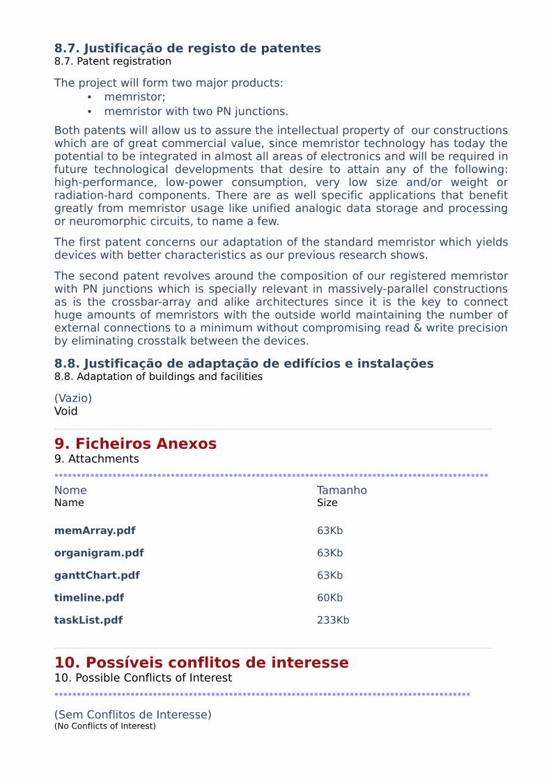
8.7. Justificação de registo de patentes8.7. Patent registration
The project will form two major products:• memristor;• memristor with two PN junctions.
Both patents will allow us to assure the intellectual property of our constructions which are of great commercial value, since memristor technology has today the potential to be integrated in almost all areas of electronics and will be required in future technological developments that desire to attain any of the following: high-performance, low-power consumption, very low size and/or weight or radiation-hard components. There are as well specific applications that benefit greatly from memristor usage like unified analogic data storage and processing or neuromorphic circuits, to name a few.
The first patent concerns our adaptation of the standard memristor which yields devices with better characteristics as our previous research shows.
The second patent revolves around the composition of our registered memristor with PN junctions which is specially relevant in massively-parallel constructions as is the crossbar-array and alike architectures since it is the key to connect huge amounts of memristors with the outside world maintaining the number of external connections to a minimum without compromising read & write precision by eliminating crosstalk between the devices.
8.8. Justificação de adaptação de edifícios e instalações8.8. Adaptation of buildings and facilities
(Vazio)Void
9. Ficheiros Anexos9. Attachments●●●●●●●●●●●●●●●●●●●●●●●●●●●●●●●●●●●●●●●●●●●●●●●●●●●●●●●●●●●●●●●●●●●●●●●●●●●●●●●●●●●●●●●●●●●●●●●●●
Nome TamanhoName Size
memArray.pdf 63Kb
organigram.pdf 63Kb
ganttChart.pdf 63Kb
timeline.pdf 60Kb
taskList.pdf 233Kb
10. Possíveis conflitos de interesse10. Possible Conflicts of Interest●●●●●●●●●●●●●●●●●●●●●●●●●●●●●●●●●●●●●●●●●●●●●●●●●●●●●●●●●●●●●●●●●●●●●●●●●●●●●●●●●●●●●●●●●●●●●
(Sem Conflitos de Interesse)(No Conflicts of Interest)


AnexosFicheiro “memArray.pdf”
Ficheiro “organigram.pdf”