Scalable Many-Core Memory Systems Lecture 2, Topic 1: DRAM Basics and DRAM Scaling

Memory Hierarchy II: Main Memory
Readings:
H&P: Chapter 5.3, Appendix C4, C5 starting at page C-53
Storage Hierarchy II: Main Memory 1

This Unit: Main Memory
• DRAM Technology
• Virtual memory• Address translation and page tables
• Virtual memory’s impact on caches
• Page-based protection
• Hardware assisted transaltion
Storage Hierarchy II: Main Memory 2
Application
OS
FirmwareCompiler
CPU I/O
Memory
Digital Circuits
Gates & Transistors

Concrete Memory Hierarchy
• 1st/2nd levels: caches (I$, D$, L2)• Made of SRAM
• Last unit
• 3rd level: main memory• Made of DRAM
• Managed in software
• This unit
• 4th level: disk (swap space)• Made of magnetic iron oxide discs
• Manage in software
• Already know (SO, OC)
Storage Hierarchy II: Main Memory 3
CPU
D$
L2
Main
Memory
I$
Disk

DRAM TECHNOLOGY
Storage Hierarchy II: Main Memory 4

RAM
• RAM: large storage arrays
• Basic structure• MxN array of bits (M N-bit words)
• This one is 4x2
• Bits in word connected by wordline
• Bits in position connected by bitline
• Operation• Address decodes into M wordlines
• High wordline word on bitlines
• Bit/bitline connection read/write
• Access latency• ~#ports * √#bits
Storage Hierarchy II: Main Memory 5
ad
dre
ss
wordline0bitlin
e1
bitlin
e0
? ?
wordline1
? ?
wordline2
? ?
wordline3
? ?
0/1
0/1
0/1
0/1 0/1
0/1
0/1
0/1
data

SRAM
• SRAM: static RAM• Bits as cross-coupled inverters (CCI)
– Four transistors per bit
– 2 additional transistors per ports
• “Static” means• Inverters connected to pwr/gnd
+ Bits naturally/continuously “refreshed”
• Designed for speed
Storage Hierarchy II: Main Memory 6
ad
dre
ss
? ?
? ?
? ?
? ?
data

DRAM
• DRAM: dynamic RAM• Bits as capacitors
+ Single transistors as ports
+ One transistor per bit/port
• “Dynamic” means• Capacitors not connected to pwr/gnd
– Stored charge decays over time
– Must be explicitly refreshed
• Designed for density• Moore’s Law
Storage Hierarchy II: Main Memory 7
ad
dre
ss
data

Moore’s Law
• Commodity DRAM parameters• 16X every 8 years is 2X every 2 years
• Not quite 2X every 18 months but still close
Storage Hierarchy II: Main Memory 8
Year Capacity $/MB Access time
1980 64Kb $1500 250ns
1988 4Mb $50 120ns
1996 64Mb $10 60ns
2004 1Gb $0.5 35ns

DRAM Operation I
• Read: similar to cache read• Phase I: pre-charge bitlines to 0.5V
• Phase II: decode address, enable wordline
• Capacitor swings bitline voltage up(down)
• Sense-amplifier interprets swing as 1(0)
– Destructive read: word bits now discharged
• Write: similar to cache write• Phase I: decode address, enable wordline
• Phase II: enable bitlines
• High bitlines charge corresponding capacitors
– What about leakage over time?
Storage Hierarchy II: Main Memory 9
ad
dre
ss
data
sa sawrite

DRAM Operation II
• Solution: add set of D-latches (row buffer)
• Read: two steps• Step I: read selected word into row buffer
• Step IIA: read row buffer out to pins
• Step IIB: write row buffer back to selected word
+ Solves “destructive read” problem
• Write: two steps• Step IA: read selected word into row buffer
• Step IB: write data into row buffer
• Step II: write row buffer back to selected word
+ Also solves leakage problem
Storage Hierarchy II: Main Memory 10
ad
dre
ss
data
sa sa
DL DL
r-I
r/w-I
r/w-II
r
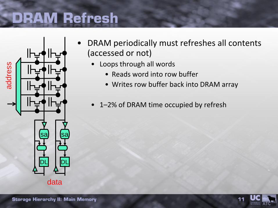
DRAM Refresh
• DRAM periodically must refreshes all contents (accessed or not)• Loops through all words
• Reads word into row buffer
• Writes row buffer back into DRAM array
• 1–2% of DRAM time occupied by refresh
Storage Hierarchy II: Main Memory 11
ad
dre
ss
data
sa sa
DL DL

DRAM
bit arrayDRAM
bit array
DRAM Parameters
• DRAM parameters• Large capacity: e.g., 64–256Mb
• Arranged as square
+ Minimizes wire length
+ Maximizes refresh efficiency
• Narrow data interface: 1–16 bit
• Cheap packages few bus pins
• Narrow address interface: N/2 addressing wires
• 16Mb DRAM has a 12-bit address bus
• How does that work?
Storage Hierarchy II: Main Memory 12
DRAM
bit array
row buffer
data
address
4K x 4K
bits4K x 4K
bits
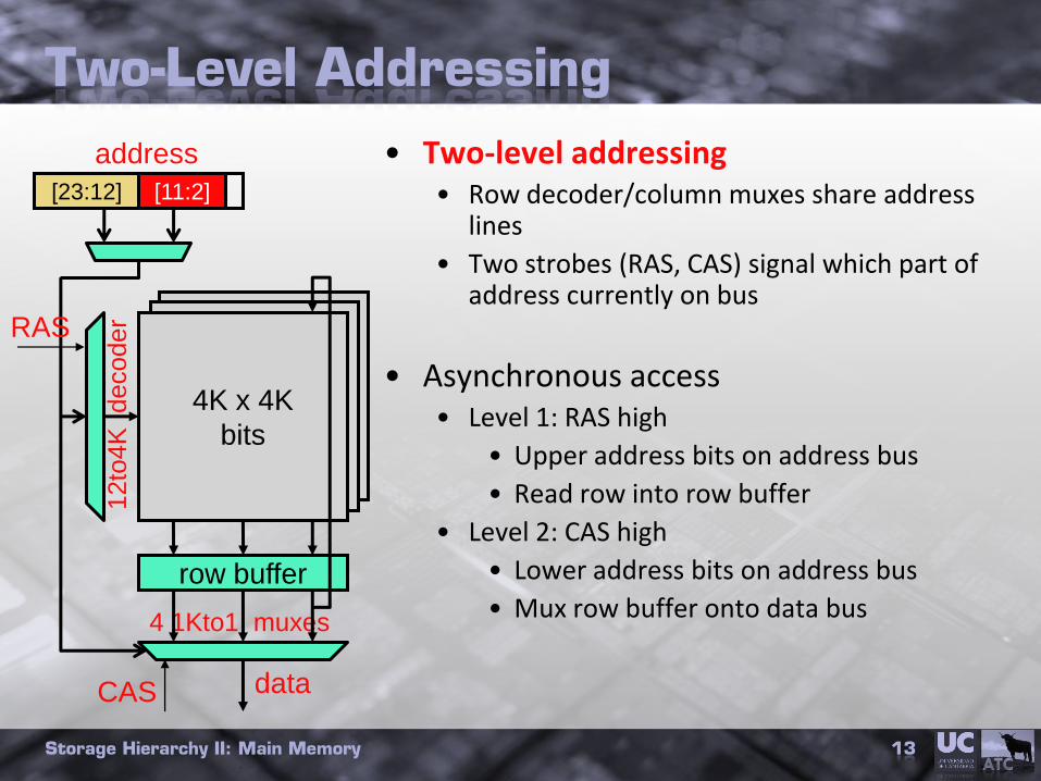
Two-Level Addressing
• Two-level addressing• Row decoder/column muxes share address
lines
• Two strobes (RAS, CAS) signal which part of address currently on bus
• Asynchronous access• Level 1: RAS high
• Upper address bits on address bus
• Read row into row buffer
• Level 2: CAS high
• Lower address bits on address bus
• Mux row buffer onto data bus
Storage Hierarchy II: Main Memory 13
4K x 4K
bits
row buffer
[23:12] [11:2]
data
address
4 1Kto1 muxes
12to
4K
d
ecoder
CAS
RAS
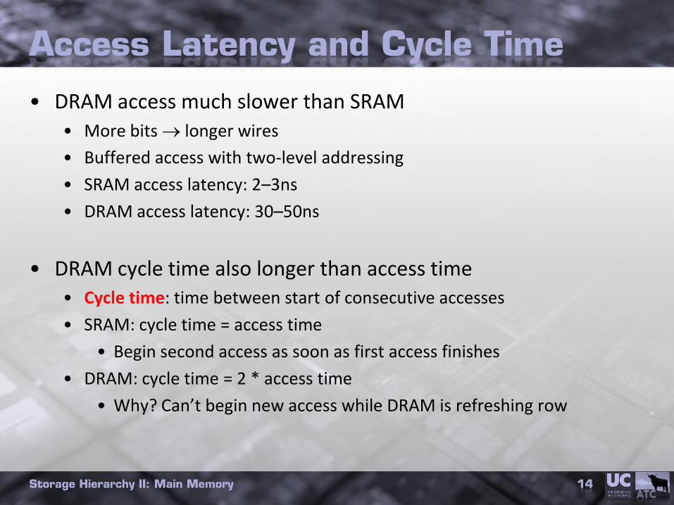
Access Latency and Cycle Time
• DRAM access much slower than SRAM
• More bits longer wires
• Buffered access with two-level addressing
• SRAM access latency: 2–3ns
• DRAM access latency: 30–50ns
• DRAM cycle time also longer than access time• Cycle time: time between start of consecutive accesses
• SRAM: cycle time = access time
• Begin second access as soon as first access finishes
• DRAM: cycle time = 2 * access time
• Why? Can’t begin new access while DRAM is refreshing row
Storage Hierarchy II: Main Memory 14

DRAM Latency and Power Derivations
• Same basic form as SRAM• Most of the equations are geometrically derived
• Same structure for decoders, wordlines, muxes
• Some differences• Somewhat different pre-charge/sensing scheme
• Array access represents smaller part of total access
• Arrays not multi-ported
Storage Hierarchy II: Main Memory 15

CS/ECE 752 (Hill): Main Memory 16
DRAM Bandwidth
• DRAM density increasing faster than demand• Result: number of memory chips per system decreasing
• Need to increase the bandwidth per chip• Especially important in game consoles
• SDRAM DDR DDR2DDR3
• Rambus/XDR - high-bandwidth memory
• Used by several game consoles

Storage Hierarchy II: Main Memory 17
Old 64MbitDRAM Example from Micron

Conventional DRAM
Storage Hierarchy II: Main Memory 18
Row add Column add
Data
RAS’
CAS’
Row add Column add
Data
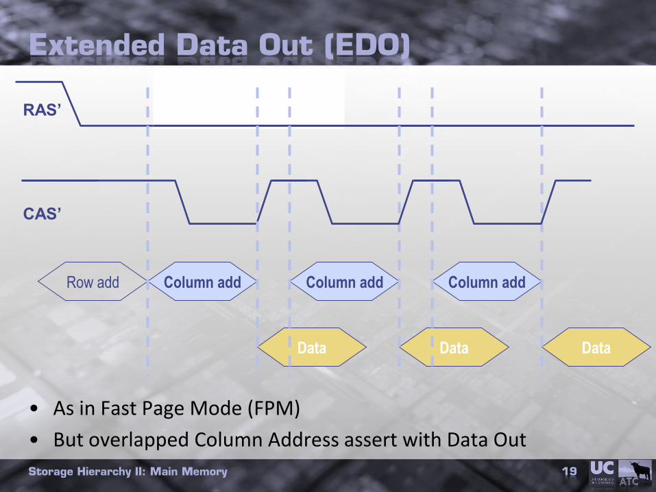
Extended Data Out (EDO)
• As in Fast Page Mode (FPM)
• But overlapped Column Address assert with Data Out
Storage Hierarchy II: Main Memory 19
Row add Column add
Data
Column add
Data
RAS’
CAS’
Column add
Data

Synchronous DRAM (SDRAM)
• Add Clock and Wider data!
• Also multiple transfers per RAS/CASStorage Hierarchy II: Main Memory 20
Row add
Column add
Data
RAS’
CAS’
Data Data

Enhanced SDRAM & DDR
• Evolutionary Enhancements on SDRAM:
1. ESDRAM (Enhanced): Overlap row buffer access with refresh
2. DDR (Double Data Rate): Transfer on both clock edges
3. DDR2/3’s small improvementslower voltage, on-chip termination, driver calibrationprefetching, conflict buffering
Storage Hierarchy II: Main Memory 21
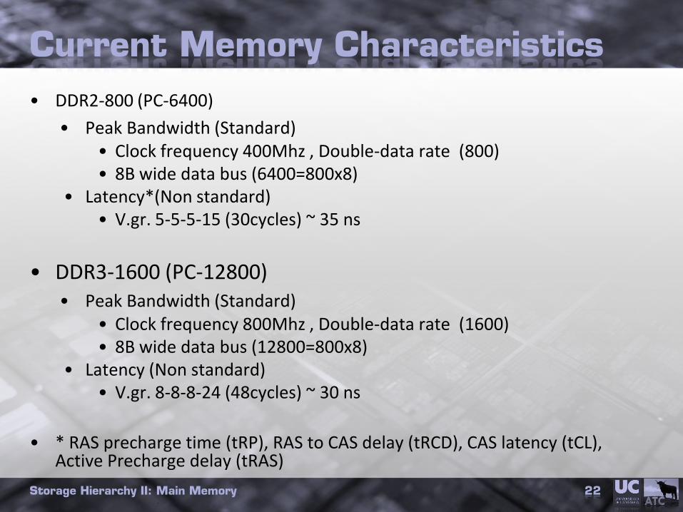
Current Memory Characteristics
• DDR2-800 (PC-6400)
• Peak Bandwidth (Standard)• Clock frequency 400Mhz , Double-data rate (800)• 8B wide data bus (6400=800x8)
• Latency*(Non standard) • V.gr. 5-5-5-15 (30cycles) ~ 35 ns
• DDR3-1600 (PC-12800)• Peak Bandwidth (Standard)
• Clock frequency 800Mhz , Double-data rate (1600)• 8B wide data bus (12800=800x8)
• Latency (Non standard)• V.gr. 8-8-8-24 (48cycles) ~ 30 ns
• * RAS precharge time (tRP), RAS to CAS delay (tRCD), CAS latency (tCL), Active Precharge delay (tRAS)
Storage Hierarchy II: Main Memory 22
Storage Hierarchy II: Main Memory 23
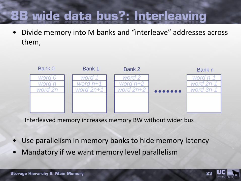
• Divide memory into M banks and “interleave” addresses across them,
Interleaved memory increases memory BW without wider bus
• Use parallelism in memory banks to hide memory latency
• Mandatory if we want memory level parallelism
Bank 0 Bank nBank 2Bank 1
word 0word n
word 2n
word 1word n+1word 2n+1
word 2word n+2word 2n+2
word n-1word 2n-1word 3n-1
8B wide data bus?: Interleaving

VIRTUAL MEMORY
Storage Hierarchy II: Main Memory 24

Storage Hierarchy II: Main Memory 25
A Computer System: Hardware
• CPUs and memories • Connected by memory bus
• I/O peripherals: storage, input, display, network, …• With separate or built-in DMA
• Connected by system bus (which is connected to memory bus)
Memory
Diskkbd
DMA DMA
display NIC
I/O ctrl
System (I/O) busMemory bus
CPU/$
bridge
CPU/$

Storage Hierarchy II: Main Memory 26
A Computer System: + App Software
• Application software: computer must do something
Memory
Diskkbd
DMA DMA
display NIC
I/O ctrl
System (I/O) busMemory bus
CPU/$
bridge
CPU/$
Application sofware

Storage Hierarchy II: Main Memory 27
A Computer System: + OS
• Operating System (OS): virtualizes hardware for apps• Abstraction: provides services (e.g., threads, files, etc.)
+ Simplifies app programming model, raw hardware is nasty
• Isolation: gives each app illusion of private CPU, memory, I/O
+ Simplifies app programming model
+ Increases hardware resource utilization
Memory
Diskkbd
DMA DMA
display NIC
I/O ctrl
System (I/O) busMemory bus
CPU/$
bridge
CPU/$
OS
Application Application Application Application

Storage Hierarchy II: Main Memory 28
Operating System (OS) and User Apps
• Sane system development requires a split• Hardware itself facilitates/enforces this split
• Operating System (OS): a super-privileged process• Manages hardware resource allocation/revocation for all processes
• Has direct access to resource allocation features
• Aware of many nasty hardware details
• Aware of other processes
• Talks directly to input/output devices (device driver software)
• User-level apps: ignorance is bliss• Unaware of most nasty hardware details
• Unaware of other apps (and OS)
• Explicitly denied access to resource allocation features

Storage Hierarchy II: Main Memory 29
System Calls
• Controlled transfers to/from OS
• System Call: a user-level app “function call” to OS• Leave description of what you want done in registers
• SYSCALL instruction (also called TRAP or INT)
• Can’t allow user-level apps to invoke arbitrary OS code
• Restricted set of legal OS addresses to jump to (trap vector)
• Processor jumps to OS using trap vector
• Change processor mode to privileged
• OS performs operation
• OS does a “return from system call”
• Unsets privileged mode

Storage Hierarchy II: Main Memory 30
Interrupts
• Exceptions: synchronous, generated by running app• E.g., illegal insn, divide by zero, etc.
• Interrupts: asynchronous events generated externally• E.g., timer, I/O request/reply, etc.
• “Interrupt” handling: same mechanism for both• “Interrupts” are on-chip signals/bits
• Either internal (e.g., timer, exceptions) or connected to pins
• Processor continuously monitors interrupt status, when one is high…
• Hardware jumps to some preset address in OS code (interrupt vector)
• Like an asynchronous, non-programmatic SYSCALL
• Timer: programmable on-chip interrupt• Initialize with some number of micro-seconds
• Timer counts down and interrupts when reaches 0

Storage Hierarchy II: Main Memory 31
Virtualizing Processors
• How do multiple apps (and OS) share the processors?• Goal: applications think there are an infinite # of processors
• Solution: time-share the resource• Trigger a context switch at a regular interval (~1ms)
• Pre-emptive: app doesn’t yield CPU, OS forcibly takes it
+ Stops greedy apps from starving others
• Architected state: PC, registers
• Save and restore them on context switches
• Memory state?
• Non-architected state: caches, branch predictor tables, etc.
• Ignore or flush
• Operating responsible to handle context switching• Hardware support is just a timer interrupt

Storage Hierarchy II: Main Memory 32
Virtualizing Main Memory
• How do multiple apps (and the OS) share main memory?• Goal: each application thinks it has infinite memory
• One app may want more memory than is in the system• App’s insn/data footprint may be larger than main memory
• Requires main memory to act like a cache
• With disk as next level in memory hierarchy (slow)
• Write-back, write-allocate, large blocks or “pages”
• No notion of “program not fitting” in registers or caches (why?)
• Solution: • Part #1: treat memory as a “cache”
• Store the overflowed blocks in “swap” space on disk
• Part #2: add a level of indirection (address translation)

Storage Hierarchy II: Main Memory 33
Virtual Memory (VM)
• Programs use virtual addresses (VA)• 0…2N–1
• VA size also referred to as machine size
• E.g., Pentium4 is 32-bit, Alpha is 64-bit
• Memory uses physical addresses (PA)• 0…2M–1 (typically M<N, especially if N=64)
• 2M is most physical memory machine supports
• VAPA at page granularity (VPPP)• By “system”
• Mapping need not preserve contiguity
• VP need not be mapped to any PP
• Unmapped VPs live on disk (swap)
…
…
Disk
Program
Main Memory
code heap stack

Storage Hierarchy II: Main Memory 34
Virtual Memory (VM)
• Virtual Memory (VM):• Level of indirection
• Application generated addresses are virtual addresses (VAs)
• Each process thinks it has its own 2N bytes of address space
• Memory accessed using physical addresses (PAs)
• VAs translated to PAs at some coarse granularity
• OS controls VA to PA mapping for itself and all other processes
• Logically: translation performed before every insn fetch, load, store
• Physically: hardware acceleration removes translation overhead
…
OS
…
App1
…
App2
VAs
PAs (physical memory)
OS controlled VAPA mappings

Storage Hierarchy II: Main Memory 35
VM is an Old Idea: Older than Caches
• Original motivation: single-program compatibility• IBM System 370: a family of computers with one software suite
+ Same program could run on machines with different memory sizes
– Prior, programmers explicitly accounted for memory size
• But also: full-associativity + software replacement• Memory tmiss is enormous: extremely important to reduce %miss
Parameter I$/D$ L2 Main Memory
thit 2ns 10ns 30ns
tmiss 10ns 30ns 10ms (10M ns)
Capacity 8–64KB 128KB–2MB 64MB–64GB
Block size 16–32B 32–256B 4+KB
Assoc./Repl. 1–4, ~LRU 4–16, ~LRU Full, “working set”

Storage Hierarchy II: Main Memory 36
Uses of Virtual Memory
• More recently: isolation and multi-programming• Each app thinks it has 2N B of memory, its stack starts 0xFFFFFFFF,…
• Apps prevented from reading/writing each other’s memory
• Can’t even address the other program’s memory!
• Protection• Each page with a read/write/execute permission set by OS
• Enforced by hardware
• Inter-process communication.• Map same physical pages into multiple virtual address spaces
• Or share files via the UNIX mmap() call
…
OS
…
App1
…
App2
Storage Hierarchy II: Main Memory 37
Disk
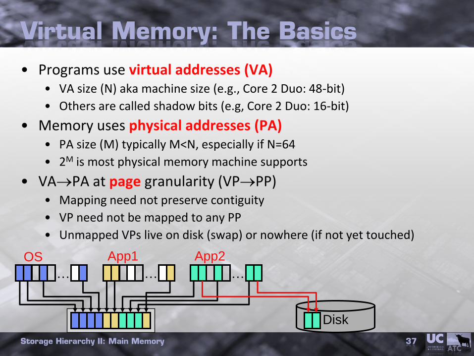
Virtual Memory: The Basics
• Programs use virtual addresses (VA)• VA size (N) aka machine size (e.g., Core 2 Duo: 48-bit)
• Others are called shadow bits (e.g, Core 2 Duo: 16-bit)
• Memory uses physical addresses (PA)• PA size (M) typically M<N, especially if N=64
• 2M is most physical memory machine supports
• VAPA at page granularity (VPPP)• Mapping need not preserve contiguity
• VP need not be mapped to any PP
• Unmapped VPs live on disk (swap) or nowhere (if not yet touched)
…
OS
…
App1
…
App2

Storage Hierarchy II: Main Memory 38
Address Translation
• VAPA mapping called address translation• Split VA into virtual page number (VPN) & page offset (POFS)
• Translate VPN into physical page number (PPN)
• POFS is not translated
• VAPA = [VPN, POFS] [PPN, POFS]
• Example above• 64KB pages 16-bit POFS
• 32-bit machine 32-bit VA 16-bit VPN
• Maximum 256MB memory 28-bit PA 12-bit PPN
POFS[15:0]virtual address[31:0] VPN[31:16]
POFS[15:0]physical address[25:0] PPN[27:16]
translate don’t touch

Storage Hierarchy II: Main Memory 39
Address Translation Mechanics I
• How are addresses translated?• In software (for now) but with hardware acceleration (a little later)
• Each process allocated a page table (PT)• Software data structure constructed by OS
• Maps VPs to PPs or to disk (swap) addresses
• VP entries empty if page never referenced
• Translation is table lookup
struct {
union { int ppn, disk_block; }
int is_valid, is_dirty;
} PTE;
struct PTE pt[NUM_VIRTUAL_PAGES];
int translate(int vpn) {
if (pt[vpn].is_valid)
return pt[vpn].ppn;
}
PT
vpn
Disk(swap)

Storage Hierarchy II: Main Memory 40
Page Table Size
• How big is a page table on the following machine?• 32-bit machine
• 4B page table entries (PTEs)
• 4KB pages
• 32-bit machine 32-bit VA 4GB virtual memory
• 4GB virtual memory / 4KB page size 1M VPs
• 1M VPs * 4B PTE 4MB
• How big would the page table be with 64KB pages?
• How big would it be for a 64-bit machine?
• Page tables can get big• There are ways of making them smaller

Storage Hierarchy II: Main Memory 41
Multi-Level Page Table (PT)
• One way: multi-level page tables• Tree of page tables
• Lowest-level tables hold PTEs
• Upper-level tables hold pointers to lower-level tables
• Different parts of VPN used to index different levels
• Example: two-level page table for machine on last slide• Compute number of pages needed for lowest-level (PTEs)
• 4KB pages / 4B PTEs 1K PTEs/page
• 1M PTEs / (1K PTEs/page) 1K pages
• Compute number of pages needed for upper-level (pointers)
• 1K lowest-level pages 1K pointers
• 1K pointers * 32-bit VA 4KB 1 upper level page

Storage Hierarchy II: Main Memory 42
Multi-Level Page Table (PT)
• 20-bit VPN• Upper 10 bits index 1st-level table
• Lower 10 bits index 2nd-level table1st-level
“pointers”
2nd-level
PTEs
VPN[9:0]VPN[19:10]
struct {
union { int ppn, disk_block; }
int is_valid, is_dirty;
} PTE;
struct {
struct PTE ptes[1024];
} L2PT;
struct L2PT *pt[1024];
int translate(int vpn) {
struct L2PT *l2pt = pt[vpn>>10];
if (l2pt && l2pt->ptes[vpn&1023].is_valid)
return l2pt->ptes[vpn&1023].ppn;
}
pt “root”

Storage Hierarchy II: Main Memory 43
Multi-Level Page Table (PT)
• Have we saved any space?• Isn’t total size of 2nd level tables same as single-level table
(i.e., 4MB)?
• Yes, but…
• Large virtual address regions unused• Corresponding 2nd-level tables need not exist
• Corresponding 1st-level pointers are null
• Example: 2MB code, 64KB stack, 16MB heap• Each 2nd-level table maps 4MB of virtual addresses
• 1 for code, 1 for stack, 4 for heap, (+1 1st-level)
• 7 total pages = 28KB (much less than 4MB)

Storage Hierarchy II: Main Memory 44
Page-Level Protection
• Page-level protection• Piggy-back page-table mechanism
• Map VPN to PPN + Read/Write/Execute permission bits
• Attempt to execute data, to write read-only data?
• Exception OS terminates program
• Useful (for OS itself actually)
struct {
union { int ppn, disk_block; }
int is_valid, is_dirty, permissions;
} PTE;
struct PTE pt[NUM_VIRTUAL_PAGES];
int translate(int vpn, int action) {
if (pt[vpn].is_valid && !(pt[vpn].permissions & action)) kill;
…
}
Storage Hierarchy II: Main Memory 45
Address Translation Mechanics II
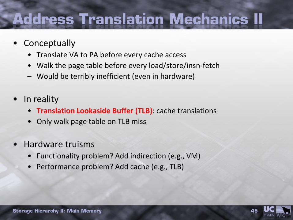
• Conceptually• Translate VA to PA before every cache access
• Walk the page table before every load/store/insn-fetch
– Would be terribly inefficient (even in hardware)
• In reality• Translation Lookaside Buffer (TLB): cache translations
• Only walk page table on TLB miss
• Hardware truisms• Functionality problem? Add indirection (e.g., VM)
• Performance problem? Add cache (e.g., TLB)

Storage Hierarchy II: Main Memory 46
Translation Buffer
• Translation buffer (TLB)• Small cache: 16–64 entries
• Associative (4+ way or fully associative)
+ Exploits temporal locality in page table
• What if an entry isn’t found in the TLB?
• Invoke TLB miss handler
VPN PPN
VPN PPN
VPN PPN
“tag” “data”
CPU
D$
L2
Main
Memory
I$
TLB
VA
PA
TLB

Storage Hierarchy II: Main Memory 47
Serial TLB & Cache Access
• “Physical” caches• Indexed and tagged by physical addresses
+ Natural, “lazy” sharing of caches between apps/OS
• VM ensures isolation (via physical addresses)
• No need to do anything on context switches
• Multi-threading works too
+ Cached inter-process communication works
• Single copy indexed by physical address
– Slow: adds at least one cycle to thit
• Note: TLBs are by definition virtual• Indexed and tagged by virtual addresses
• Flush across context switches
• Or extend with process id tags
CPU
D$
L2
Main
Memory
I$
TLB
VA
PA
TLB

Storage Hierarchy II: Main Memory 48
Parallel TLB & Cache Access
• What about parallel access? • What if
(cache size) / (associativity) ≤ page size
• Index bits same in virt. and physical addresses!
• Access TLB in parallel with cache • Cache access needs tag only at very end
+ Fast: no additional thit cycles
+ No context-switching/aliasing problems
• Dominant organization used today
• Example: Pentium 4, 4KB pages, 8KB, 2-way SA L1 data cache• Implication: associativity allows bigger caches
CPU
D$
L2
Main
Memory
I$TLBVA
PATLB
[4:0]tag [31:12] index [11:5]
VPN [31:16] page offset [15:0]
?
page offset [15:0]PPN[27:16]

Storage Hierarchy II: Main Memory 49
TLB Organization
• Like caches: TLBs also have ABCs• Capacity
• Associativity (At least 4-way associative, fully-associative common)
• What does it mean for a TLB to have a block size of two?
• Two consecutive VPs share a single tag
• Like caches: there can be L2 TLBs
• Example: AMD Opteron• 32-entry fully-assoc. TLBs, 512-entry 4-way L2 TLB (insn & data)
• 4KB pages, 48-bit virtual addresses, four-level page table
• Rule of thumb: TLB should “cover” L2 contents• In other words: (#PTEs in TLB) * page size ≥ L2 size
• Why? Think about relative miss latency in each…

Storage Hierarchy II: Main Memory 50
TLB Misses
• TLB miss: translation not in TLB, but in page table• Two ways to “fill” it, both relatively fast
• Software-managed TLB: e.g., Alpha • Short (~10 insn) OS routine walks page table, updates TLB
+ Keeps page table format flexible
– Latency: one or two memory accesses + OS call (pipeline flush)
• Hardware-managed TLB: e.g., x86• Page table root pointer in hardware register, FSM “walks” table
+ Latency: saves cost of OS call (pipeline flush)
– Page table format is hard-coded

Storage Hierarchy II: Main Memory 51
Page Faults
• Page fault: PTE not in TLB or page table
• page not in memory
• Starts out as a TLB miss, detected by OS/hardware handler
• OS software routine:• Choose a physical page to replace
• “Working set”: refined LRU, tracks active page usage
• If dirty, write to disk
• Read missing page from disk
• Takes so long (~10ms), OS schedules another task
• Requires yet another data structure: frame map (why?)
• Treat like a normal TLB miss from here

Acknowledgments
• Slides developed by Amir Roth of University of Pennsylvania with sources that included University of Wisconsin slides by Mark Hill, Guri Sohi, Jim Smith, and David Wood.
• Slides enhanced by Milo Martin and Mark Hill with sources that included Profs. Asanovic, Falsafi, Hoe, Lipasti, Shen, Smith, Sohi, Vijaykumar, and Wood
• Slides re-enhanced by V. Puente
Memory Hierarchy I: Caches 52