Memory COE 308 Computer Architecture Prof. Muhamed Mudawar Computer Engineering Department King Fahd...
62
Memory COE 308 Computer Architecture Prof. Muhamed Mudawar Computer Engineering Department King Fahd University of Petroleum and Minerals
-
Upload
kaylyn-edman -
Category
Documents
-
view
220 -
download
0
Transcript of Memory COE 308 Computer Architecture Prof. Muhamed Mudawar Computer Engineering Department King Fahd...

Memory
COE 308
Computer Architecture
Prof. Muhamed Mudawar
Computer Engineering Department
King Fahd University of Petroleum and Minerals

Memory COE 308 – Computer Architecture© Muhamed Mudawar – slide 2
Presentation Outline
Random Access Memory and its Structure
Memory Hierarchy and the need for Cache Memory
The Basics of Caches
Cache Performance and Memory Stall Cycles
Improving Cache Performance
Multilevel Caches

Memory COE 308 – Computer Architecture© Muhamed Mudawar – slide 3
Large arrays of storage cells
Volatile memory
Hold the stored data as long as it is powered on
Random Access
Access time is practically the same to any data on a RAM chip
Chip Select (CS) control signal
Select RAM chip to read/write
Read/Write (R/W) control signal
Specifies memory operation
2n × m RAM chip: n-bit address and m-bit data
Random Access Memory
RAM
Address
Data
CS R/W
n
m

Memory COE 308 – Computer Architecture© Muhamed Mudawar – slide 4
Row decoder
Select row to read/write
Column decoder
Select column to read/write
Cell Matrix
2D array of tiny memory cells
Sense/Write amplifiers
Sense & amplify data on read
Drive bit line with data in on write
Same data lines are used for data in/out
Typical Memory Structure
Row
add
ress
10
. . .
. . . 1024 × 1024
Cell Matrix
Row
Dec
oder
Sense/write amplifiers
Column Decoder
. . .
Column address
10
Data
R / W

Memory COE 308 – Computer Architecture© Muhamed Mudawar – slide 5
Static RAM Storage Cell Static RAM (SRAM): fast but expensive RAM
6-Transistor cell with no static current
Typically used for caches
Provides fast access time
Cell Implementation:
Cross-coupled inverters store bit
Two pass transistors
Row decoder selects the word line
Pass transistors enable the cell to be read and written
Typical SRAM cell
Vcc
Word line
bit bit

Memory COE 308 – Computer Architecture© Muhamed Mudawar – slide 6
Dynamic RAM Storage Cell Dynamic RAM (DRAM): slow, cheap, and dense memory
Typical choice for main memory
Cell Implementation:
1-Transistor cell (pass transistor)
Trench capacitor (stores bit)
Bit is stored as a charge on capacitor
Must be refreshed periodically
Because of leakage of charge from tiny capacitor
Refreshing for all memory rows
Reading each row and writing it back to restore the charge
Typical DRAM cell
Word line
bit
Capacitor
PassTransistor

Memory COE 308 – Computer Architecture© Muhamed Mudawar – slide 7
DRAM Refresh Cycles
Time
Threshold voltage
0 Stored
1 Written Refreshed Refreshed Refreshed
Refresh Cycle
Voltage for 1
Voltage for 0
Refresh cycle is about tens of milliseconds
Refreshing is done for the entire memory
Each row is read and written back to restore the charge
Some of the memory bandwidth is lost to refresh cycles

Memory COE 308 – Computer Architecture© Muhamed Mudawar – slide 8
Loss of Bandwidth to Refresh Cycles
Example:
A 256 Mb DRAM chip
Organized internally as a 16K 16K cell matrix
Rows must be refreshed at least once every 50 ms
Refreshing a row takes 100 ns
What fraction of the memory bandwidth is lost to refresh cycles?
Solution:
Refreshing all 16K rows takes: 16 1024 100 ns = 1.64 ms
Loss of 1.64 ms every 50 ms
Fraction of lost memory bandwidth = 1.64 / 50 = 3.3%

Memory COE 308 – Computer Architecture© Muhamed Mudawar – slide 9
Typical DRAM Packaging 24-pin dual in-line package for 16Mbit = 222 4 memory
22-bit address is divided into
11-bit row address
11-bit column address
Interleaved on same address lines
1 2 3 4 5 6 7 8 9 10 11 12
24 23 22 21 20 19 18 17 16 15 14 13
A4 A5 A6 A7 A8 A9 D3 D4 CAS OE Vss Vss
A0 A1 A2 A3 A10 D1 D2 RAS WE Vcc Vcc NC
Legend
AiCASDjNCOERASWE
Address bit i Column address strobeData bit j No connectionOutput enableRow address strobeWrite enable
Memory COE 308 – Computer Architecture© Muhamed Mudawar – slide 10
Trends in DRAMDRAM capacity quadrupled every three years until 1996
After 1996, DRAM capacity doubled every two years
Year introduced
Capacity Cost per MBTotal access time
to a new rowColumn access to existing row
1980 64 Kbit $1500.00 250 ns 150 ns
1983 256 Kbit $500.00 185 ns 100 ns
1985 1 Mbit $200.00 135 ns 40 ns
1989 4 Mbit $50.00 110 ns 40 ns
1992 16 Mbit $15.00 90 ns 30 ns
1996 64 Mbit $10.00 60 ns 12 ns
1998 128 Mbit $4.00 60 ns 10 ns
2000 256 Mbit $1.00 55 ns 7 ns
2002 512 Mbit $0.25 50 ns 5 ns
2004 1024 Mbit $0.10 45 ns 3 ns
Memory COE 308 – Computer Architecture© Muhamed Mudawar – slide 11
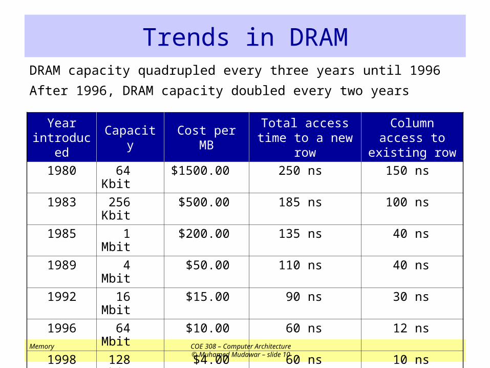
Expanding the Data Bus Width Memory chips typically have a narrow data bus
We can expand the data bus width by a factor of p
Use p RAM chips and feed the same address to all chips
Use the same Chip Select and Read/Write control signals
CS R/W
Address
Data
CS R/W
Address
Data
CS R/W
Address
Data
. . .
Data width = m × p bits
. .m m

Memory COE 308 – Computer Architecture© Muhamed Mudawar – slide 12
Increasing Memory Capacity by 2k
A k to 2k decoder is used to select one of the 2k chips
Upper n bits of address is fed to all memory chips
Lower k bits of address are decoded to select one of the 2k chips
CS R/W
Address
Data
CS R/W
Address
Data
CS R/W
Address
Data
. . .
Data width = m bitsm m mm
k to 2k
decodern
n+k
. . .
k
Add
ress Data bus of all chips are wired together
Only the selected chip will read/write the data
Memory COE 308 – Computer Architecture© Muhamed Mudawar – slide 13
Next . . .
Random Access Memory and its Structure
Memory Hierarchy and the need for Cache Memory
The Basics of Caches
Cache Performance and Memory Stall Cycles
Improving Cache Performance
Multilevel Caches

Memory COE 308 – Computer Architecture© Muhamed Mudawar – slide 14
Processor-Memory Performance Gap
1980 – No cache in microprocessor
1995 – Two-level cache on microprocessor
CPU: 55% per year
DRAM: 7% per year1
10
100
10001
98
01
98
1
19
83
19
84
19
85
19
86
19
87
19
88
19
89
19
90
19
91
19
92
19
93
19
94
19
95
19
96
19
97
19
98
19
99
20
00
19
82
Processor-MemoryPerformance Gap:(grows 50% per year)
Per
form
ance
“Moore’s Law”

Memory COE 308 – Computer Architecture© Muhamed Mudawar – slide 15
The Need for Cache Memory Widening speed gap between CPU and main memory
Processor operation takes less than 1 ns
Main memory requires more than 50 ns to access
Each instruction involves at least one memory access
One memory access to fetch the instruction
A second memory access for load and store instructions
Memory bandwidth limits the instruction execution rate
Cache memory can help bridge the CPU-memory gap
Cache memory is small in size but fast

Memory COE 308 – Computer Architecture© Muhamed Mudawar – slide 16
Typical Memory Hierarchy Registers are at the top of the hierarchy
Typical size < 1 KB
Access time < 0.5 ns
Level 1 Cache (8 – 64 KB) Access time: 0.5 – 1 ns
L2 Cache (512KB – 8MB) Access time: 2 – 10 ns
Main Memory (1 – 2 GB) Access time: 50 – 70 ns
Disk Storage (> 200 GB) Access time: milliseconds
Microprocessor
Registers
L1 Cache
L2 Cache
Memory
Disk, Tape, etc
Memory Bus
I/O Bus
Fas
ter
Big
ger
Memory COE 308 – Computer Architecture© Muhamed Mudawar – slide 17
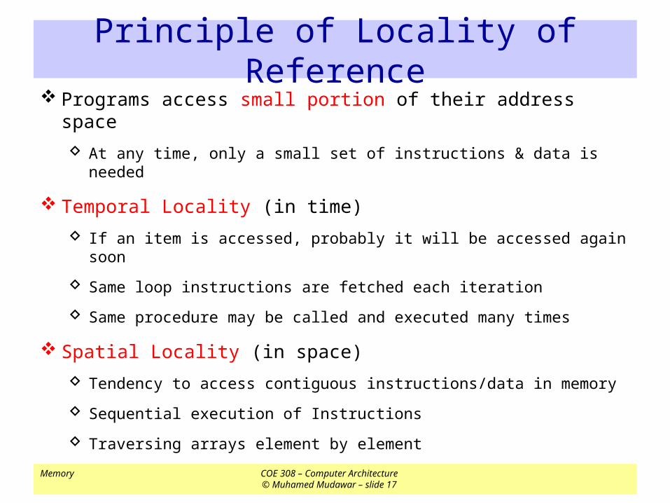
Principle of Locality of Reference Programs access small portion of their address space
At any time, only a small set of instructions & data is needed
Temporal Locality (in time)
If an item is accessed, probably it will be accessed again soon
Same loop instructions are fetched each iteration
Same procedure may be called and executed many times
Spatial Locality (in space)
Tendency to access contiguous instructions/data in memory
Sequential execution of Instructions
Traversing arrays element by element

Memory COE 308 – Computer Architecture© Muhamed Mudawar – slide 18
What is a Cache Memory ? Small and fast (SRAM) memory technology
Stores the subset of instructions & data currently being accessed
Used to reduce average access time to memory
Caches exploit temporal locality by …
Keeping recently accessed data closer to the processor
Caches exploit spatial locality by …
Moving blocks consisting of multiple contiguous words
Goal is to achieve
Fast speed of cache memory access
Balance the cost of the memory system

Memory COE 308 – Computer Architecture© Muhamed Mudawar – slide 19
Cache Memories in the Datapath
Address
Rs
Rt Register
File
Imm26
Rw
ALU
res
ult
BBA
Imm
16R
w
mux
mux
Inst
ruct
ion
mux
mux
Instruction
Cache
Address
Instruction
Inc
PC
00
mux
ALU
NP
CExt
Imm16
Next
PC
PCSrc
Data
Cache
Address
Data_in
ALU result
mux
Writ
eDat
aR
w
Rd
Main Memory
Control
Data
Interface between CPU and memory
Memory COE 308 – Computer Architecture© Muhamed Mudawar – slide 20
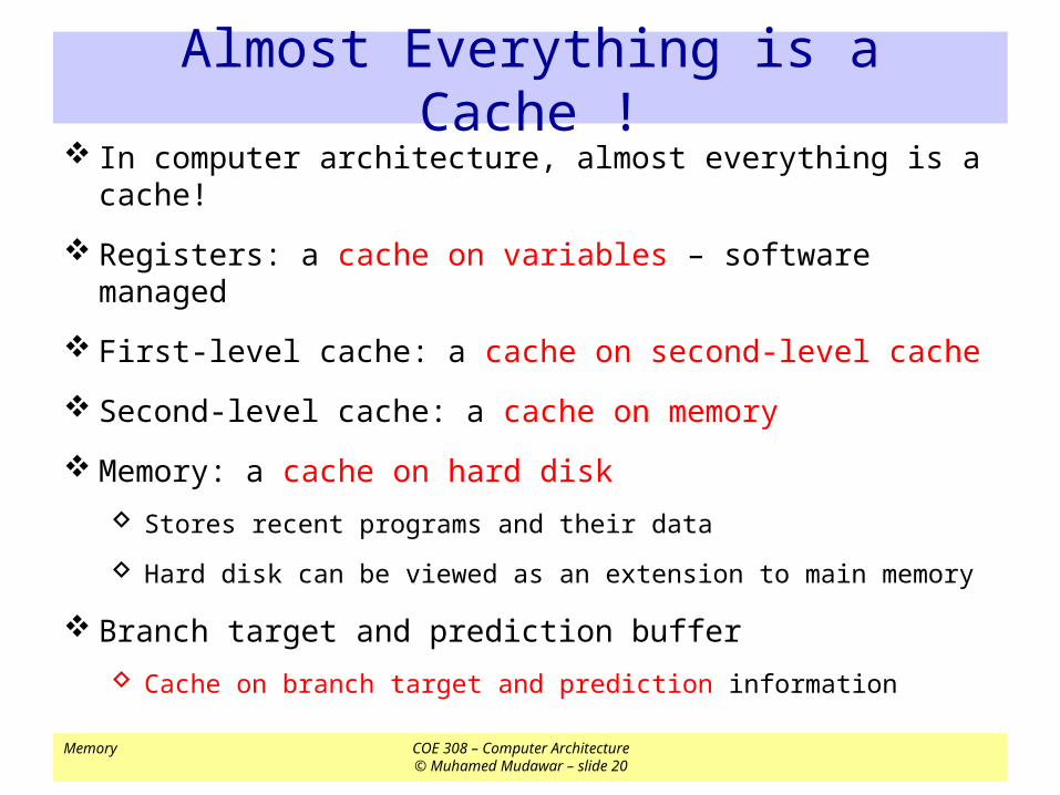
Almost Everything is a Cache ! In computer architecture, almost everything is a cache!
Registers: a cache on variables – software managed
First-level cache: a cache on second-level cache
Second-level cache: a cache on memory
Memory: a cache on hard disk
Stores recent programs and their data
Hard disk can be viewed as an extension to main memory
Branch target and prediction buffer
Cache on branch target and prediction information

Memory COE 308 – Computer Architecture© Muhamed Mudawar – slide 21
Next . . .
Random Access Memory and its Structure
Memory Hierarchy and the need for Cache Memory
The Basics of Caches
Cache Performance and Memory Stall Cycles
Improving Cache Performance
Multilevel Caches

Memory COE 308 – Computer Architecture© Muhamed Mudawar – slide 22
Four Basic Questions on Caches Q1: Where can a block be placed in a cache?
Block placement
Direct Mapped, Set Associative, Fully Associative
Q2: How is a block found in a cache? Block identification
Block address, tag, index
Q3: Which block should be replaced on a miss? Block replacement
FIFO, Random, LRU
Q4: What happens on a write? Write strategy
Write Back or Write Through (with Write Buffer)

Memory COE 308 – Computer Architecture© Muhamed Mudawar – slide 23
Block Placement: Direct Mapped Block: unit of data transfer between cache and memory
Direct Mapped Cache: A block can be placed in exactly one location in the cache
000
001
010
011
100
101
110
111
000
0000
001
000
1000
011
001
0000
101
001
1000
111
010
0001
001
010
1001
011
011
0001
101
011
1001
111
100
0010
001
100
1010
011
101
0010
101
101
1010
111
110
0011
001
110
1011
011
111
0011
101
111
1011
111
In this example:
Cache index =least significant 3 bits of Memory address
Cac
he
Mai
nM
emor
y

Memory COE 308 – Computer Architecture© Muhamed Mudawar – slide 24
Direct-Mapped Cache A memory address is divided into
Block address: identifies block in memory
Block offset: to access bytes within a block
A block address is further divided into Index: used for direct cache access
Tag: most-significant bits of block address
Index = Block Address mod Cache Blocks
Tag must be stored also inside cache For block identification
A valid bit is also required to indicate Whether a cache block is valid or not
V Tag Block Data
=
Hit
Data
Tag Index offset
Block Address

Memory COE 308 – Computer Architecture© Muhamed Mudawar – slide 25
Direct Mapped Cache – cont’d Cache hit: block is stored inside cache
Index is used to access cache block
Address tag is compared against stored tag
If equal and cache block is valid then hit
Otherwise: cache miss
If number of cache blocks is 2n
n bits are used for the cache index
If number of bytes in a block is 2b
b bits are used for the block offset
If 32 bits are used for an address 32 – n – b bits are used for the tag
Cache data size = 2n+b bytes
V Tag Block Data
=
Hit
Data
Tag Index offset
Block Address

Memory COE 308 – Computer Architecture© Muhamed Mudawar – slide 26
Mapping an Address to a Cache Block
Example Consider a direct-mapped cache with 256 blocks
Block size = 16 bytes
Compute tag, index, and byte offset of address: 0x01FFF8AC
Solution 32-bit address is divided into:
4-bit byte offset field, because block size = 24 = 16 bytes
8-bit cache index, because there are 28 = 256 blocks in cache
20-bit tag field
Byte offset = 0xC = 12 (least significant 4 bits of address)
Cache index = 0x8A = 138 (next lower 8 bits of address)
Tag = 0x01FFF (upper 20 bits of address)
Tag Index offset
4820
Block Address

Memory COE 308 – Computer Architecture© Muhamed Mudawar – slide 27
Example on Cache Placement & Misses
Consider a small direct-mapped cache with 32 blocks Cache is initially empty, Block size = 16 bytes
The following memory addresses (in decimal) are referenced:
1000, 1004, 1008, 2548, 2552, 2556.
Map addresses to cache blocks and indicate whether hit or miss
Solution: 1000 = 0x3E8 cache index = 0x1E Miss (first access) 1004 = 0x3EC cache index = 0x1E Hit 1008 = 0x3F0 cache index = 0x1F Miss (first access) 2548 = 0x9F4 cache index = 0x1F Miss (different tag) 2552 = 0x9F8 cache index = 0x1F Hit 2556 = 0x9FC cache index = 0x1F Hit
Tag Index offset
4523

Memory COE 308 – Computer Architecture© Muhamed Mudawar – slide 28
Fully Associative Cache A block can be placed anywhere in cache no indexing
If m blocks exist then m comparators are needed to match tag
Cache data size = m 2b bytes
m-way associative
Address
Tag offset
DataHit
= = = =
V Tag Block DataV Tag Block DataV Tag Block DataV Tag Block Data
mux

Memory COE 308 – Computer Architecture© Muhamed Mudawar – slide 29
Set-Associative Cache A set is a group of blocks that can be indexed
A block is first mapped onto a set
Set index = Block address mod Number of sets in cache
If there are m blocks in a set (m-way set associative) then
m tags are checked in parallel using m comparators
If 2n sets exist then set index consists of n bits
Cache data size = m 2n+b bytes (with 2b bytes per block)
Without counting tags and valid bits
A direct-mapped cache has one block per set (m = 1)
A fully-associative cache has one set (2n = 1 or n = 0)

Memory COE 308 – Computer Architecture© Muhamed Mudawar – slide 30
Set-Associative Cache Diagram
m-way set-associative
V Tag Block DataV Tag Block DataV Tag Block DataV Tag Block Data
Address Tag Index offset
Data
= = = =
muxHit

Memory COE 308 – Computer Architecture© Muhamed Mudawar – slide 31
Write Policy Write Through:
Writes update cache and lower-level memory
Cache control bit: only a Valid bit is needed
Memory always has latest data, which simplifies data coherency
Can always discard cached data when a block is replaced
Write Back: Writes update cache only
Cache control bits: Valid and Modified bits are required
Modified cached data is written back to memory when replaced
Multiple writes to a cache block require only one write to memory
Uses less memory bandwidth than write-through and less power
However, more complex to implement than write through

Memory COE 308 – Computer Architecture© Muhamed Mudawar – slide 32
Write Miss Policy What happens on a write miss?
Write Allocate: Allocate new block in cache
Write miss acts like a read miss, block is fetched and updated
No Write Allocate: Send data to lower-level memory
Cache is not modified
Typically, write back caches use write allocate Hoping subsequent writes will be captured in the cache
Write-through caches often use no-write allocate Reasoning: writes must still go to lower level memory

Memory COE 308 – Computer Architecture© Muhamed Mudawar – slide 33
Write Buffer Decouples the CPU write from the memory bus writing
Permits writes to occur without stall cycles until buffer is full
Write-through: all stores are sent to lower level memory
Write buffer eliminates processor stalls on consecutive writes
Write-back: modified blocks are written when replaced
Write buffer is used for evicted blocks that must be written back
The address and modified data are written in the buffer
The write is finished from the CPU perspective
CPU continues while the write buffer prepares to write memory
If buffer is full, CPU stalls until buffer has an empty entry

Memory COE 308 – Computer Architecture© Muhamed Mudawar – slide 34
What Happens on a Cache Miss? Cache sends a miss signal to stall the processor
Decide which cache block to allocate/replace One choice only when the cache is directly mapped
Multiple choices for set-associative or fully-associative cache
Transfer the block from lower level memory to this cache Set the valid bit and the tag field from the upper address bits
If block to be replaced is modified then write it back Modified block is moved into a Write Buffer
Otherwise, block to be replaced can be simply discarded
Restart the instruction that caused the cache miss
Miss Penalty: clock cycles to process a cache miss

Memory COE 308 – Computer Architecture© Muhamed Mudawar – slide 35
Replacement Policy Which block to be replaced on a cache miss?
No selection alternatives for direct-mapped caches
m blocks per set to choose from for associative caches
Random replacement Candidate blocks are randomly selected
One counter for all sets (0 to m – 1): incremented on every cycle
On a cache miss replace block specified by counter
First In First Out (FIFO) replacement Replace oldest block in set
One counter per set (0 to m – 1): specifies oldest block to replace
Counter is incremented on a cache miss

Memory COE 308 – Computer Architecture© Muhamed Mudawar – slide 36
Replacement Policy – cont’d Least Recently Used (LRU)
Replace block that has been unused for the longest time
Order blocks within a set from least to most recently used
Update ordering of blocks on each cache hit
With m blocks per set, there are m! possible permutations
Pure LRU is too costly to implement when m > 2 m = 2, there are 2 permutations only (a single bit is needed)
m = 4, there are 4! = 24 possible permutations
LRU approximation are used in practice
For large m > 4,
Random replacement can be as effective as LRU

Memory COE 308 – Computer Architecture© Muhamed Mudawar – slide 37
Comparing Random, FIFO, and LRU
Data cache misses per 1000 instructions 10 SPEC2000 benchmarks on Alpha processor
Block size of 64 bytes
LRU and FIFO outperforming Random for a small cache
Little difference between LRU and Random for a large cache
LRU is expensive for large associativity (# blocks per set)
Random is the simplest to implement in hardware2-way 4-way 8-way
Size LRU Rand FIFO LRU Rand FIFO LRU Rand FIFO
16 KB 114.1 117.3 115.5 111.7 115.1 113.3 109.0 111.8 110.4
64 KB 103.4 104.3 103.9 102.4 102.3 103.1 99.7 100.5 100.3
256 KB 92.2 92.1 92.5 92.1 92.1 92.5 92.1 92.1 92.5

Memory COE 308 – Computer Architecture© Muhamed Mudawar – slide 38
Next . . .
Random Access Memory and its Structure
Memory Hierarchy and the need for Cache Memory
The Basics of Caches
Cache Performance and Memory Stall Cycles
Improving Cache Performance
Multilevel Caches

Memory COE 308 – Computer Architecture© Muhamed Mudawar – slide 39
Hit Rate and Miss Rate Hit Rate = Hits / (Hits + Misses)
Miss Rate = Misses / (Hits + Misses)
I-Cache Miss Rate = Miss rate in the Instruction Cache
D-Cache Miss Rate = Miss rate in the Data Cache
Example: Out of 1000 instructions fetched, 150 missed in the I-Cache
25% are load-store instructions, 50 missed in the D-Cache
What are the I-cache and D-cache miss rates?
I-Cache Miss Rate = 150 / 1000 = 15%
D-Cache Miss Rate = 50 / (25% × 1000) = 50 / 250 = 20%

Memory COE 308 – Computer Architecture© Muhamed Mudawar – slide 40
The processor stalls on a Cache miss When fetching instructions from the Instruction Cache (I-cache)
When loading or storing data into the Data Cache (D-cache)
Memory stall cycles = Combined Misses Miss Penalty
Miss Penalty: clock cycles to process a cache miss
Combined Misses = I-Cache Misses + D-Cache Misses
I-Cache Misses = I-Count × I-Cache Miss Rate
D-Cache Misses = LS-Count × D-Cache Miss Rate
LS-Count (Load & Store) = I-Count × LS Frequency
Cache misses are often reported per thousand instructions
Memory Stall Cycles

Memory COE 308 – Computer Architecture© Muhamed Mudawar – slide 41
Memory Stall Cycles Per Instruction
Memory Stall Cycles Per Instruction =
Combined Misses Per Instruction × Miss Penalty
Miss Penalty is assumed equal for I-cache & D-cache
Miss Penalty is assumed equal for Load and Store
Combined Misses Per Instruction =
I-Cache Miss Rate + LS Frequency × D-Cache Miss Rate
Therefore, Memory Stall Cycles Per Instruction =
I-Cache Miss Rate × Miss Penalty +
LS Frequency × D-Cache Miss Rate × Miss Penalty

Memory COE 308 – Computer Architecture© Muhamed Mudawar – slide 42
Example on Memory Stall Cycles Consider a program with the given characteristics
Instruction count (I-Count) = 106 instructions
30% of instructions are loads and stores
D-cache miss rate is 5% and I-cache miss rate is 1%
Miss penalty is 100 clock cycles for instruction and data caches
Compute combined misses per instruction and memory stall cycles
Combined misses per instruction in I-Cache and D-Cache 1% + 30% 5% = 0.025 combined misses per instruction
Equal to 25 misses per 1000 instructions
Memory stall cycles 0.025 100 (miss penalty) = 2.5 stall cycles per instruction
Total memory stall cycles = 106 2.5 = 2,500,000

Memory COE 308 – Computer Architecture© Muhamed Mudawar – slide 43
CPU Time with Memory Stall Cycles
CPIPerfectCache = CPI for ideal cache (no cache misses)
CPIMemoryStalls = CPI in the presence of memory stalls
Memory stall cycles increase the CPI
CPU Time = I-Count × CPIMemoryStalls × Clock Cycle
CPIMemoryStalls = CPIPerfectCache + Mem Stalls per Instruction

Memory COE 308 – Computer Architecture© Muhamed Mudawar – slide 44
Example on CPI with Memory Stalls
A processor has CPI of 1.5 without any memory stalls Cache miss rate is 2% for instruction and 5% for data
20% of instructions are loads and stores
Cache miss penalty is 100 clock cycles for I-cache and D-cache
What is the impact on the CPI?
Answer:
Mem Stalls per Instruction =
CPIMemoryStalls =
CPIMemoryStalls / CPIPerfectCache =
Processor is 3 times slower due to memory stall cycles
CPINoCache =
Instruction data
0.02×100 + 0.2×0.05×100 = 3
1.5 + 3 = 4.5 cycles per instruction
4.5 / 1.5 = 3
1.5 + (1 + 0.2) × 100 = 121.5 (a lot worse)

Memory COE 308 – Computer Architecture© Muhamed Mudawar – slide 45
Average Memory Access Time Average Memory Access Time (AMAT)
AMAT = Hit time + Miss rate × Miss penalty
Time to access a cache for both hits and misses
Example: Find the AMAT for a cache with
Cache access time (Hit time) of 1 cycle = 2 ns
Miss penalty of 20 clock cycles
Miss rate of 0.05 per access
Solution:
AMAT = 1 + 0.05 × 20 = 2 cycles = 4 ns
Without the cache, AMAT will be equal to Miss penalty = 20 cycles

Memory COE 308 – Computer Architecture© Muhamed Mudawar – slide 46
Designing Memory to Support Caches
Bus
CPU
Memory
Cache
One
-wor
d-w
ide
Mem
ory
Org
aniz
atio
n
Cache
Multiplexer
Bus
Memory
Wide Memory Organization
CPU
Memory
bank 0
Memory
bank 1
Memory
bank 2
Memory
bank 3
Interleaved Memory Organization
Bus
CPU
Cache
One Word Wide: CPU, Cache, Bus, and Memory have word width: 32 or 64 bits
Interleaved: CPU, Cache, Bus: 1 wordMemory: N independent banks
Wide: CPU, Mux: 1 wordCache, Bus, Memory: N wordsAlpha: 256 bitsUltra SPARC: 512 bits

Memory COE 308 – Computer Architecture© Muhamed Mudawar – slide 47
Memory Interleaving Memory interleaving is more flexible than wide access
A block address is sent only once to all memory banks
Words of a block are distributed (interleaved) across all banks
Banks are accessed in parallel
Words are transferred one at a time on each bus cycle
Memory
bank 0
Memory
bank 1
Memory
bank 2
Memory
bank 3
Interleaved Memory Organization
Bus
CPU
Cache
Time
Buscycle
All banks accesssame block address
word 3 (bank 3)
word 2 (bank 2)
word 1 (bank 1)
word 0 (bank 0)
blo
ck
ad
dre
ss

Memory COE 308 – Computer Architecture© Muhamed Mudawar – slide 48
Estimating the Miss Penalty Timing Model: Assume the following …
1 memory bus cycle to send address
15 memory bus cycles for DRAM access time
1 memory bus cycle to send data
Cache Block is 4 words
One-Word-Wide Memory Organization
Miss Penalty = 1 + 4 ×15 + 4 × 1 = 65 memory bus cycles
Wide Memory Organization (2-word wide)
Miss Penalty = 1 + 2 ×15 + 2 × 1 = 33 memory bus cycles
Interleaved Memory Organization (4 banks)
Miss Penalty = 1 + 1 ×15 + 4 × 1 = 20 memory bus cycles

Memory COE 308 – Computer Architecture© Muhamed Mudawar – slide 49
Next . . .
Random Access Memory and its Structure
Memory Hierarchy and the need for Cache Memory
The Basics of Caches
Cache Performance and Memory Stall Cycles
Improving Cache Performance
Multilevel Caches

Memory COE 308 – Computer Architecture© Muhamed Mudawar – slide 50
Improving Cache Performance
Average Memory Access Time (AMAT)
AMAT = Hit time + Miss rate * Miss penalty
Used as a framework for optimizations
Reduce the Hit time
Small and simple caches
Reduce the Miss Rate
Larger cache size, higher associativity, and larger block size
Reduce the Miss Penalty
Multilevel caches

Memory COE 308 – Computer Architecture© Muhamed Mudawar – slide 51
Small and Simple Caches Hit time is critical: affects the processor clock cycle
Fast clock rate demands small and simple L1 cache designs
Small cache reduces the indexing time and hit time Indexing a cache represents a time consuming portion
Tag comparison also adds to this hit time
Direct-mapped overlaps tag check with data transfer Associative cache uses additional mux and increases hit time
Size of L1 caches has not increased much L1 caches are the same size on Alpha 21264 and 21364
Same also on UltraSparc II and III, AMD K6 and Athlon
Reduced from 16 KB in Pentium III to 8 KB in Pentium 4

Memory COE 308 – Computer Architecture© Muhamed Mudawar – slide 52
Classifying Misses – Three Cs Conditions under which misses occur
Compulsory: program starts with no block in cache
Also called cold start misses
Misses that would occur even if a cache has infinite size
Capacity: misses happen because cache size is finite
Blocks are replaced and then later retrieved
Misses that would occur in a fully associative cache of a finite size
Conflict: misses happen because of limited associativity
Limited number of blocks per set
Non-optimal replacement algorithm

Memory COE 308 – Computer Architecture© Muhamed Mudawar – slide 53
Classifying Misses – cont’d
Compulsory misses are independent of cache size
Very small for long-running programs
Conflict misses decrease as associativity increases
Data were collected using LRU replacement
Capacity misses decrease as capacity increases
Miss Rate
0
2%
4%
6%
8%
10%
12%
14%
1 2 4 8 16 32 64 128 KB
1-way
2-way
4-way
8-way
Capacity Compulsor
y

Memory COE 308 – Computer Architecture© Muhamed Mudawar – slide 54
Larger Size and Higher Associativity
Increasing cache size reduces capacity misses
It also reduces conflict misses
Larger cache size spreads out references to more blocks
Drawbacks: longer hit time and higher cost
Larger caches are especially popular as 2nd level caches
Higher associativity also improves miss rates
Eight-way set associative is as effective as a fully associative

Memory COE 308 – Computer Architecture© Muhamed Mudawar – slide 55
Larger Block Size Simplest way to reduce miss rate is to increase block size
However, it increases conflict misses if cache is small
Block Size (bytes)
Mis
s R
ate
0%
5%
10%
15%
20%
25%
16
32
64
128
256
1K
4K
16K
64K
256K
Increased Conflict Misses
Reduced Compulsory Misses
64-byte blocks are
common in L1 caches
128-byte block are
common in L2 caches

Memory COE 308 – Computer Architecture© Muhamed Mudawar – slide 56
Next . . .
Random Access Memory and its Structure
Memory Hierarchy and the need for Cache Memory
The Basics of Caches
Cache Performance and Memory Stall Cycles
Improving Cache Performance
Multilevel Caches

Memory COE 308 – Computer Architecture© Muhamed Mudawar – slide 57
Multilevel Caches Top level cache should be kept small to
Keep pace with processor speed
Adding another cache level Can reduce the memory gap
Can reduce memory bus loading
Local miss rate Number of misses in a cache / Memory accesses to this cache
Miss RateL1 for L1 cache, and Miss RateL2 for L2 cache
Global miss rate
Number of misses in a cache / Memory accesses generated by CPU
Miss RateL1 for L1 cache, and Miss RateL1 Miss RateL2 for L2 cache
Unified L2 Cache
I-Cache D-Cache
Main Memory

Memory COE 308 – Computer Architecture© Muhamed Mudawar – slide 58
Multilevel Cache Policies Multilevel Inclusion
L1 cache data is always present in L2 cache
A miss in L1, but a hit in L2 copies block from L2 to L1
A miss in L1 and L2 brings a block into L1 and L2
A write in L1 causes data to be written in L1 and L2
Typically, write-through policy is used from L1 to L2
Typically, write-back policy is used from L2 to main memory
To reduce traffic on the memory bus
A replacement or invalidation in L2 must be propagated to L1

Memory COE 308 – Computer Architecture© Muhamed Mudawar – slide 59
Multilevel Cache Policies – cont’d Multilevel exclusion
L1 data is never found in L2 cache – Prevents wasting space
Cache miss in L1, but a hit in L2 results in a swap of blocks
Cache miss in both L1 and L2 brings the block into L1 only
Block replaced in L1 is moved into L2
Example: AMD Athlon
Same or different block size in L1 and L2 caches
Choosing a larger block size in L2 can improve performance
However different block sizes complicates implementation
Pentium 4 has 64-byte blocks in L1 and 128-byte blocks in L2

Memory COE 308 – Computer Architecture© Muhamed Mudawar – slide 60
Two-Level Cache Performance – 1/2
Average Memory Access Time:
AMAT = Hit TimeL1 + Miss RateL1 Miss PenaltyL1
Miss Penalty for L1 cache in the presence of L2 cache
Miss PenaltyL1 = Hit TimeL2 + Miss RateL2 Miss PenaltyL2
Average Memory Access Time with a 2nd Level cache:
AMAT = Hit TimeL1 + Miss RateL1
(Hit TimeL2 + Miss RateL2 Miss PenaltyL2)
Memory Stall Cycles per Instruction =
Memory Access per Instruction × (AMAT – Hit TimeL1)
Memory COE 308 – Computer Architecture© Muhamed Mudawar – slide 61
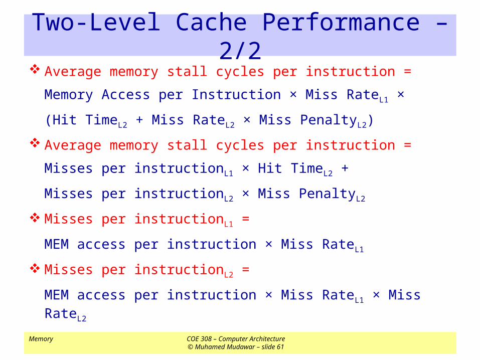
Two-Level Cache Performance – 2/2 Average memory stall cycles per instruction =
Memory Access per Instruction × Miss RateL1 ×
(Hit TimeL2 + Miss RateL2 × Miss PenaltyL2)
Average memory stall cycles per instruction =
Misses per instructionL1 × Hit TimeL2 +
Misses per instructionL2 × Miss PenaltyL2
Misses per instructionL1 =
MEM access per instruction × Miss RateL1
Misses per instructionL2 =
MEM access per instruction × Miss RateL1 × Miss RateL2

Memory COE 308 – Computer Architecture© Muhamed Mudawar – slide 62
Example on Two-Level Caches Problem:
Miss RateL1 = 4%, Miss RateL2 = 25%
Hit time of L1 cache is 1 cycle and of L2 cache is 10 cycles
Miss penalty from L2 cache to memory is 100 cycles
Memory access per instruction = 1.25 (25% data accesses)
Compute AMAT and memory stall cycles per instruction
Solution:AMAT = 1 + 4% × (10 + 25% × 100) = 2.4 cycles
Misses per instruction in L1 = 4% × 1.25 = 5%
Misses per instruction in L2 = 4% × 25% × 1.25 = 1.25%
Memory stall cycles per instruction = 5% × 10 + 1.25% × 100 = 1.75
Can be also obtained as: (2.4 – 1) × 1.25 = 1.75 cycles