
Medium Energy Ion Scattering Technique and Applications
34
Medium Energy Ion Scattering – Technique and Applications Dr Tim Noakes STFC Daresbury Laboratory, Daresbury Science and Innovation Campus, Keckwick Lane, Daresbury, Warrington, Cheshire, WA4 4AD, UK
Transcript of Medium Energy Ion Scattering Technique and Applications
Medium Energy Ion
Scattering – Technique
and Applications
Dr Tim Noakes
STFC Daresbury Laboratory, Daresbury Science and
Innovation Campus, Keckwick Lane, Daresbury,
Warrington, Cheshire, WA4 4AD, UK
Overview
•The medium-energy ion scattering (MEIS)
technique
•Applications of MEIS
• Surface structure
• High resolution depth profiling
• Thin film characterisation
• Characterisation of nanostructures
•Possible future research areas
•Summary
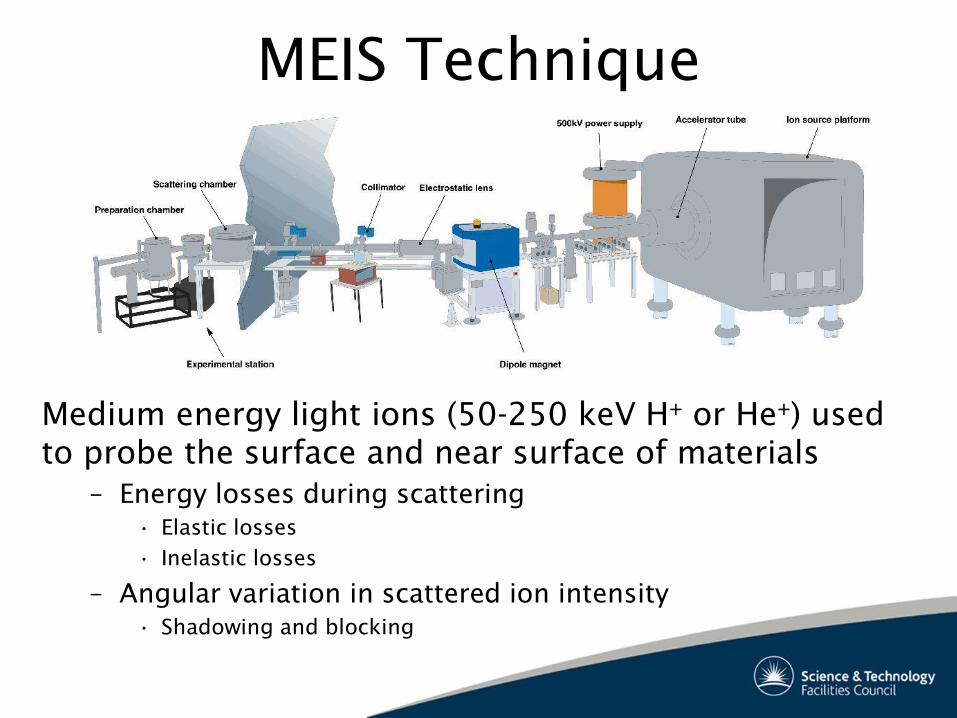
MEIS Technique
Medium energy light ions (50-250 keV H+ or He
+) used
to probe the surface and near surface of materials
– Energy losses during scattering
• Elastic losses
• Inelastic losses
– Angular variation in scattered ion intensity
• Shadowing and blocking
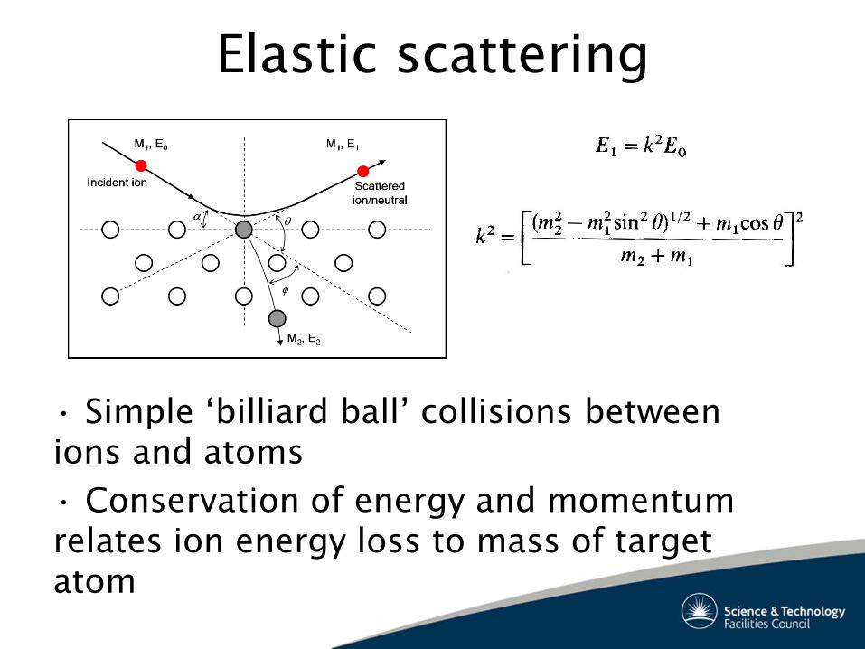
Elastic scattering
• Simple ‘billiard ball’ collisions between
ions and atoms
• Conservation of energy and momentum
relates ion energy loss to mass of target
atom
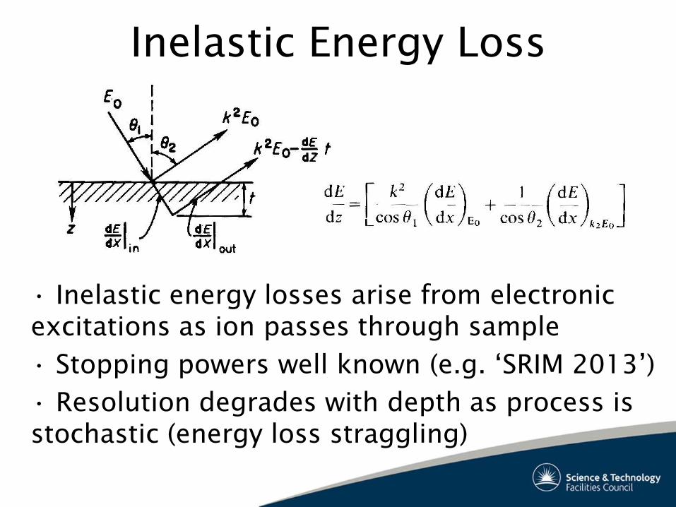
Inelastic Energy Loss
• Inelastic energy losses arise from electronic
excitations as ion passes through sample
• Stopping powers well known (e.g. ‘SRIM 2013’)
• Resolution degrades with depth as process is
stochastic (energy loss straggling)
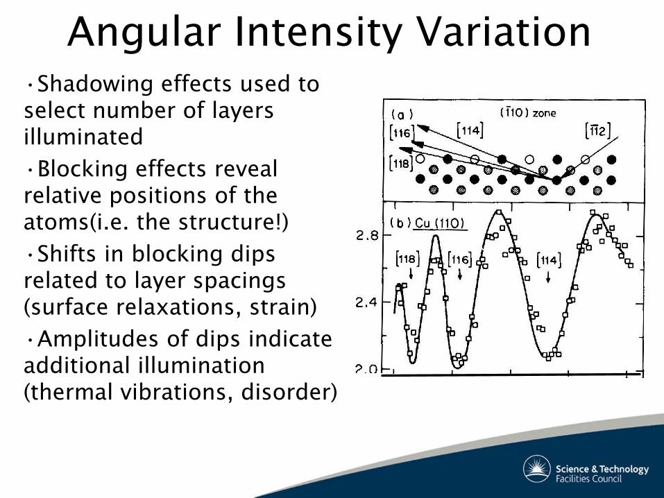
Angular Intensity Variation
•Shadowing effects used to
select number of layers
illuminated
•Blocking effects reveal
relative positions of the
atoms(i.e. the structure!)
•Shifts in blocking dips
related to layer spacings
(surface relaxations, strain)
•Amplitudes of dips indicate
additional illumination
(thermal vibrations, disorder)
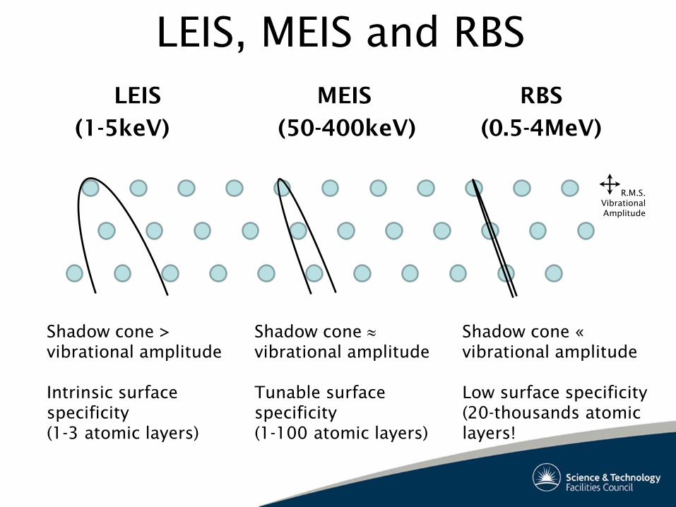
LEIS, MEIS and RBS
LEIS MEIS RBS
(1-5keV) (50-400keV) (0.5-4MeV)
Shadow cone >
vibrational amplitude
Intrinsic surface
specificity
(1-3 atomic layers)
Shadow cone
vibrational amplitude
Tunable surface
specificity
(1-100 atomic layers)
Shadow cone «
vibrational amplitude
Low surface specificity
(20-thousands atomic
layers!
R.M.S.
Vibrational
Amplitude
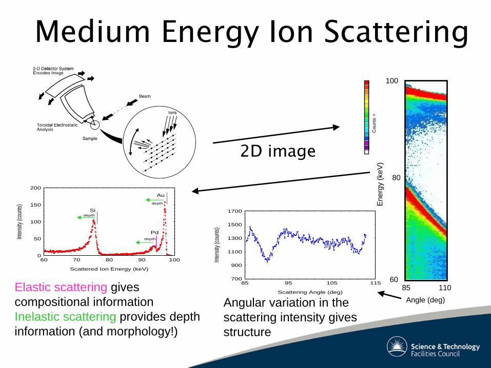
Medium Energy Ion Scattering
2D image
Angle (deg)
En
erg
y (
ke
V)
100
80
60 85 110
Counts
>
0
50
100
150
200
60 70 80 90 100
depth
depth
depth
Si
Pd
Au
Scattered Ion Energy (keV)
Inte
nsity
(cou
nts)
700
900
1100
1300
1500
1700
85 95 105 115
Scattering Angle (deg)
Inte
nsity
(cou
nts)
Elastic scattering gives
compositional information
Inelastic scattering provides depth
information (and morphology!)
Angular variation in the
scattering intensity gives
structure
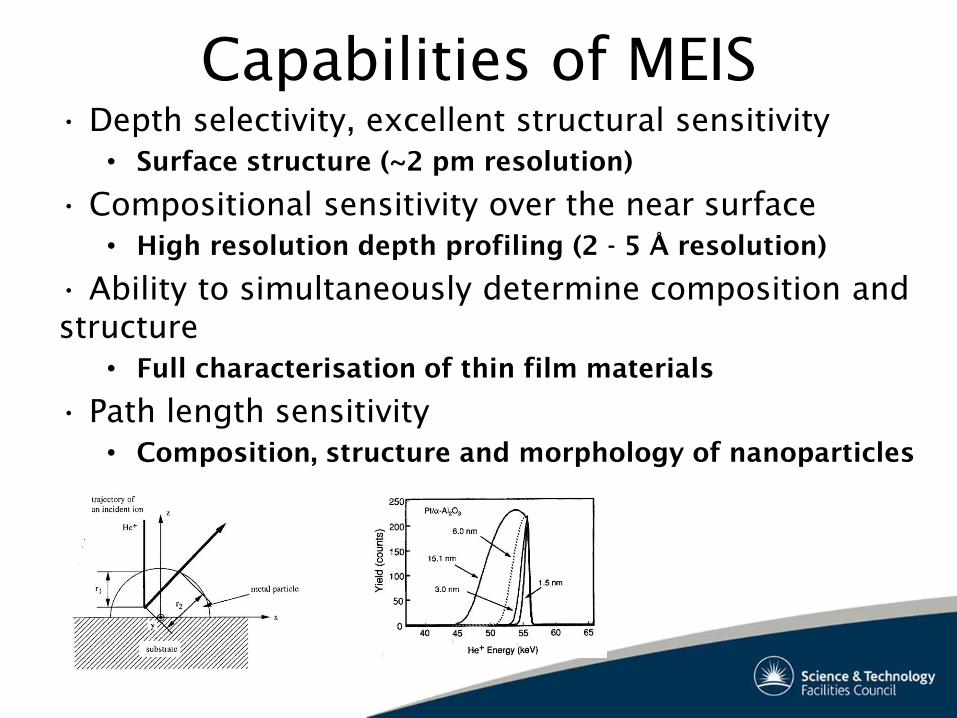
Capabilities of MEIS
• Depth selectivity, excellent structural sensitivity
• Surface structure (~2 pm resolution)
• Compositional sensitivity over the near surface
• High resolution depth profiling (2 - 5 Å resolution)
• Ability to simultaneously determine composition and
structure
• Full characterisation of thin film materials
• Path length sensitivity
• Composition, structure and morphology of nanoparticles
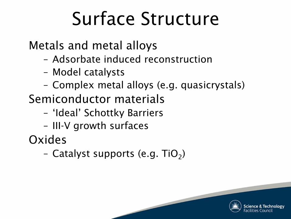
Surface Structure
Metals and metal alloys
– Adsorbate induced reconstruction
– Model catalysts
– Complex metal alloys (e.g. quasicrystals)
Semiconductor materials
– ‘Ideal’ Schottky Barriers
– III-V growth surfaces
Oxides
– Catalyst supports (e.g. TiO2)
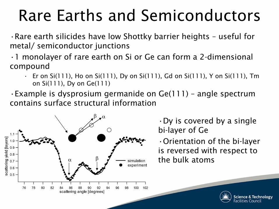
Rare Earths and Semiconductors
•Rare earth silicides have low Shottky barrier heights – useful for
metal/ semiconductor junctions
•1 monolayer of rare earth on Si or Ge can form a 2-dimensional
compound
• Er on Si(111), Ho on Si(111), Dy on Si(111), Gd on Si(111), Y on Si(111), Tm
on Si(111), Dy on Ge(111)
•Example is dysprosium germanide on Ge(111) – angle spectrum
contains surface structural information
•Dy is covered by a single
bi-layer of Ge
•Orientation of the bi-layer
is reversed with respect to
the bulk atoms
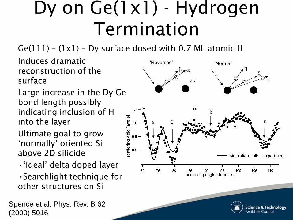
Dy on Ge(1x1) - Hydrogen
Termination
Ge(111) – (1x1) – Dy surface dosed with 0.7 ML atomic H
e
e
Induces dramatic
reconstruction of the
surface
Large increase in the Dy-Ge
bond length possibly
indicating inclusion of H
into the layer
Ultimate goal to grow
‘normally’ oriented Si
above 2D silicide
•‘Ideal’ delta doped layer
•Searchlight technique for
other structures on Si
‘Reversed’ ‘Normal’
Spence et al, Phys. Rev. B 62
(2000) 5016
High Resolution Depth Profiling
Semiconductor device fabrication
• Ion implants for semiconductor devices
• High- gate dielectric materials
Structural materials
• Oxide layers for Corrosion protection of light metal
alloys
• Construction materials
• Automotive, aerospace, rail and marine transport applications
•Biocompatible coatings for medical implants
MEIS of ALD grown high-K films
•MEIS energy spectra sensitive to
both sub-surface SiOx growth and
re-crystallisation
•Quantitative information on sub-
surface oxide thickness obtained
by fitting data with simulated
spectra
•Moore’s Law (ITRS) requires high dielectric constant
gate oxides to reduce leakage currents
•Amorphous Hafnium oxide has high permittivity
but high temperature processing can cause sub-
surface SiO2 growth and film re-crystallisation
re-crystallisation
increased thickness
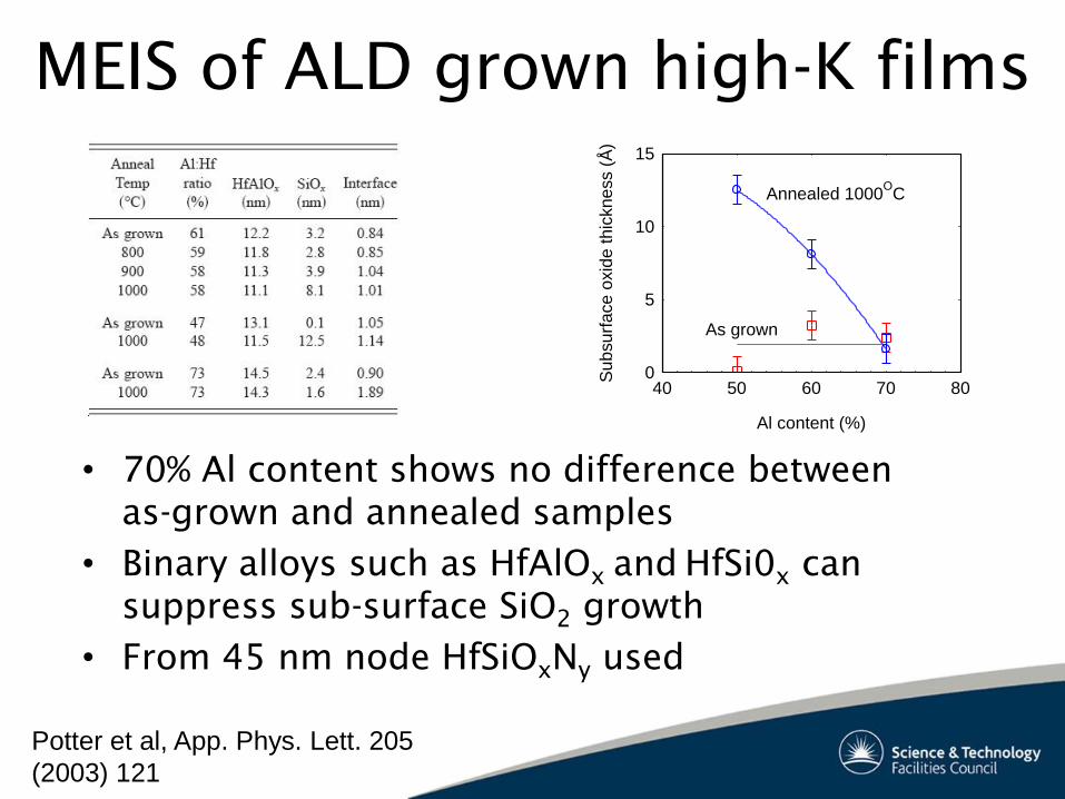
MEIS of ALD grown high-K films
• 70% Al content shows no difference between
as-grown and annealed samples
• Binary alloys such as HfAlOx
and HfSi0
x can
suppress sub-surface SiO2 growth
• From 45 nm node HfSiOxN
y used
0
5
10
15
40 50 60 70 80
As grown
Annealed 1000OC
Al content (%)
Su
bsu
rface
oxid
e t
hic
kn
ess (
Å)
Potter et al, App. Phys. Lett. 205
(2003) 121
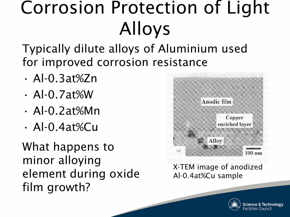
Corrosion Protection of Light
Alloys
Typically dilute alloys of Aluminium used
for improved corrosion resistance
• Al-0.3at%Zn
• Al-0.7at%W
• Al-0.2at%Mn
• Al-0.4at%Cu
What happens to
minor alloying
element during oxide
film growth?
X-TEM image of anodized
Al-0.4at%Cu sample
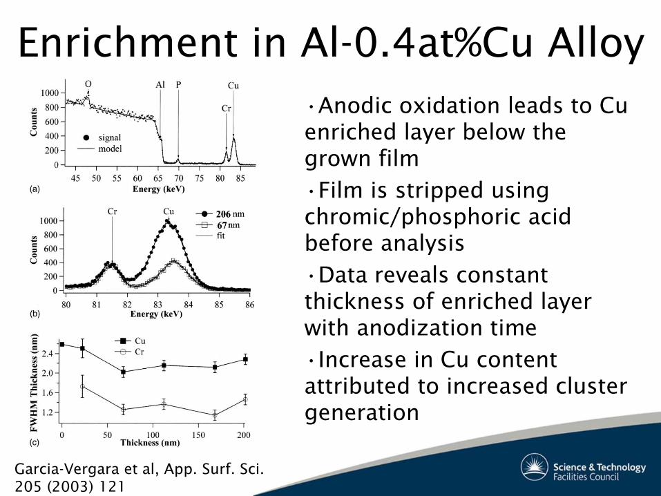
Enrichment in Al-0.4at%Cu Alloy
•Anodic oxidation leads to Cu
enriched layer below the
grown film
•Film is stripped using
chromic/phosphoric acid
before analysis
•Data reveals constant
thickness of enriched layer
with anodization time
•Increase in Cu content
attributed to increased cluster
generation
Garcia-Vergara et al, App. Surf. Sci.
205 (2003) 121
Thin Film Characterisation
Systems which benefit from the
simultaneous elucidation of composition
and structure
• Metal-on-metal growth (giant magneto-
resistance films)
• Quantum well systems (III-V materials, metals)
• Spintronic materials (metal/semiconductor
hybrids)
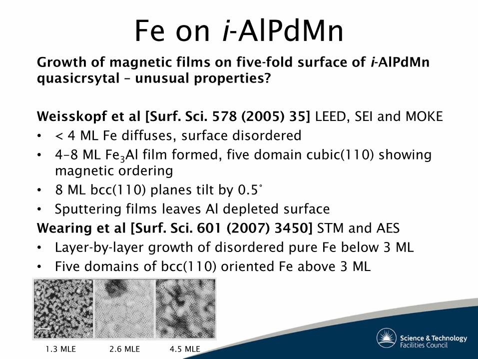
Fe on i-AlPdMn
Growth of magnetic films on five-fold surface of i-AlPdMn
quasicrsytal – unusual properties?
Weisskopf et al [Surf. Sci. 578 (2005) 35] LEED, SEI and MOKE
• < 4 ML Fe diffuses, surface disordered
• 4–8 ML Fe3Al film formed, five domain cubic(110) showing
magnetic ordering
• 8 ML bcc(110) planes tilt by 0.5°
• Sputtering films leaves Al depleted surface
Wearing et al [Surf. Sci. 601 (2007) 3450] STM and AES
• Layer-by-layer growth of disordered pure Fe below 3 ML
• Five domains of bcc(110) oriented Fe above 3 ML
1.3 MLE 2.6 MLE 4.5 MLE
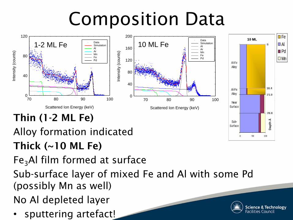
Composition Data
Thin (1-2 ML Fe)
Alloy formation indicated
Thick (~10 ML Fe)
Fe3Al film formed at surface
Sub-surface layer of mixed Fe and Al with some Pd
(possibly Mn as well)
No Al depleted layer
• sputtering artefact!
0
40
80
120
160
200
70 80 90 100
DataSimulationAlArMnFePd
Scattered Ion Energy (keV)
Inte
nsity (
co
un
ts)
0
40
80
120
70 80 90 100
DataSimulationAlArMnFePd
Scattered Ion Energy (keV)
Inte
nsity (
co
un
ts)
1-2 ML Fe 10 ML Fe
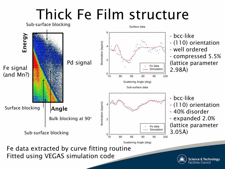
Thick Fe Film structure En
erg
y
Angle
Bulk blocking at 90
Surface blocking
Sub-surface blocking
Sub-surface blocking
Pd signal
Fe signal
(and Mn?)
Fe data extracted by curve fitting routine
Fitted using VEGAS simulation code
0
2
4
6
75 80 85 90 95 100
Fe dataSimulation
Scattering Angle (deg)
Illu
min
atio
n (
laye
rs)
Surface data
- bcc-like
- (110) orientation
- well ordered
- compressed 5.5%
(lattice parameter
2.98Å)
0
2
4
75 80 85 90 95 100
Fe dataSimulation
Scattering Angle (deg)
Illu
min
atio
n (
laye
rs)
Sub-surface data
- bcc-like
- (110) orientation
- 40% disorder
- expanded 2.0%
(lattice parameter
3.05Å)
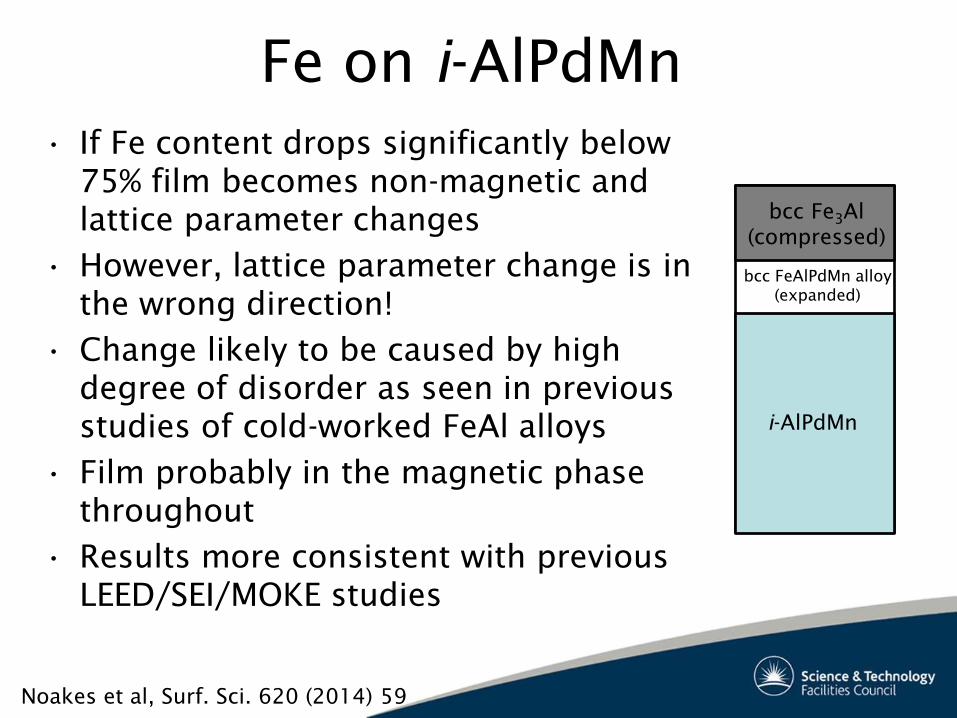
Fe on i-AlPdMn
bcc Fe3Al
(compressed)
bcc FeAlPdMn alloy
(expanded)
i-AlPdMn
• If Fe content drops significantly below
75% film becomes non-magnetic and
lattice parameter changes
• However, lattice parameter change is in
the wrong direction!
• Change likely to be caused by high
degree of disorder as seen in previous
studies of cold-worked FeAl alloys
• Film probably in the magnetic phase
throughout
• Results more consistent with previous
LEED/SEI/MOKE studies
Noakes et al, Surf. Sci. 620 (2014) 59
Nanoparticle Characterisation
Topographical information
• Single element clusters
Compositional information
• Bimetallic alloys (model catalysts)
• III-V quantum dots
Structural Information
• All the above!
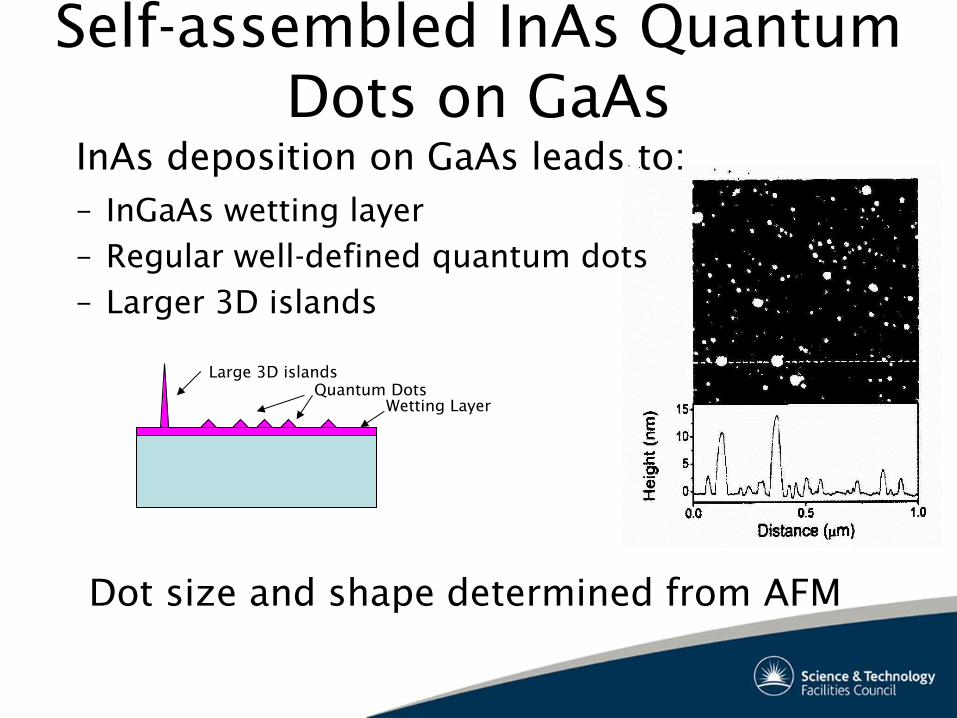
Self-assembled InAs Quantum
Dots on GaAs
Dot size and shape determined from AFM
Large 3D islands Quantum Dots
Wetting Layer
InAs deposition on GaAs leads to:
– InGaAs wetting layer
– Regular well-defined quantum dots
– Larger 3D islands
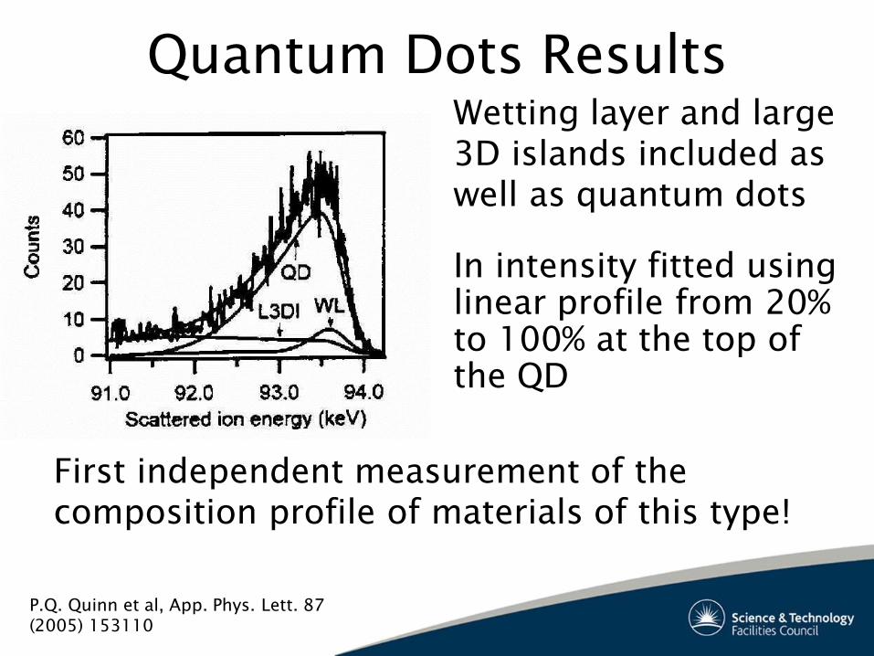
Quantum Dots Results
First independent measurement of the
composition profile of materials of this type!
Wetting layer and large
3D islands included as
well as quantum dots
In intensity fitted using
linear profile from 20%
to 100% at the top of
the QD
P.Q. Quinn et al, App. Phys. Lett. 87
(2005) 153110
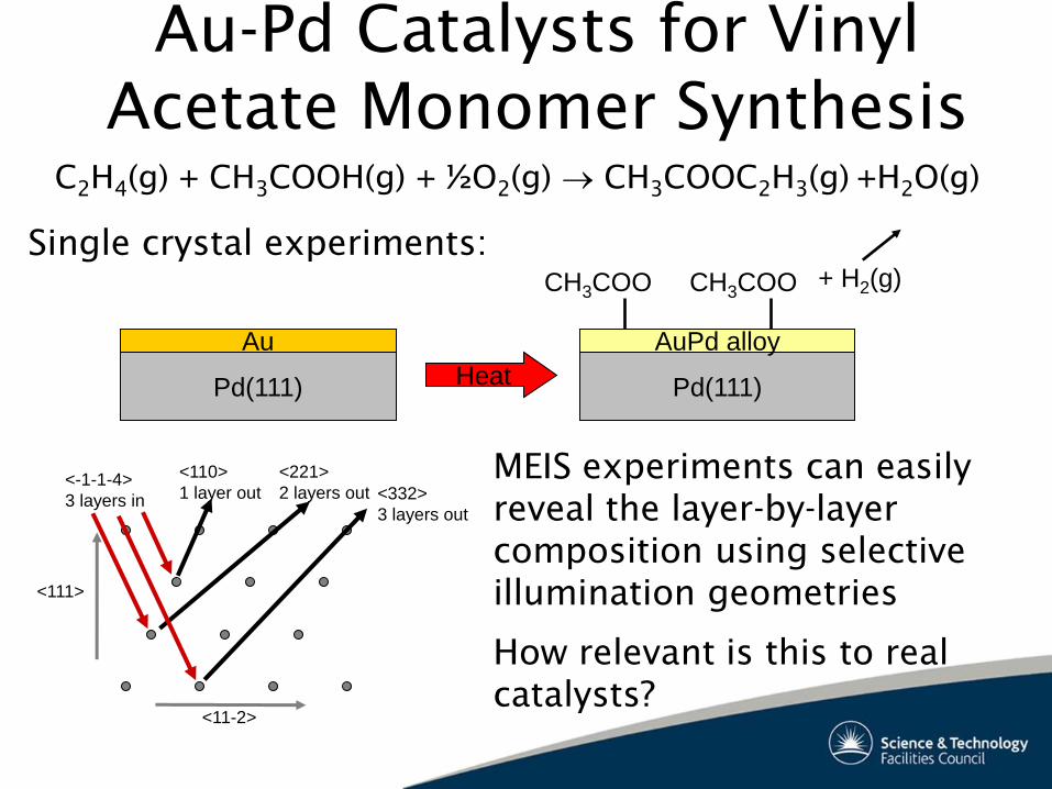
Au-Pd Catalysts for Vinyl
Acetate Monomer Synthesis
C2H
4(g) + CH
3COOH(g) + ½O
2(g) CH
3COOC
2H
3(g)
+H
2O(g)
Single crystal experiments:
Pd(111)
Au
Heat Pd(111)
AuPd alloy
CH3COO CH3COO + H2(g)
<111>
<11-2>
<-1-1-4>
3 layers in <332>
3 layers out
<221>
2 layers out
<110>
1 layer out MEIS experiments can easily
reveal the layer-by-layer
composition using selective
illumination geometries
How relevant is this to real
catalysts?
Au-Pd Clusters on SiO2/Si(100)
c-Si(001)
-SiO2
AuPd AuPd
c-Si(001)
-SiO2
AuPd AuPd
CH3COO CH3COO
Heat AcOH
c-Si(001)
-SiO2
AuPd 2nm
0
20
40
60
80
100450°C
0
20
40
60
80
85 90 95 100
680°C
Scattered Ion Energy
0
20
40
60
80
100600°C
Inte
nsity (
co
un
ts)
Detailed fitting of the
MEIS energy spectra
including information
on cluster size and
coverage
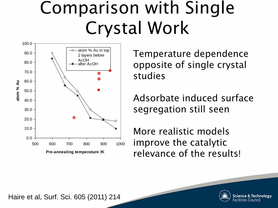
Comparison with Single
Crystal Work
0.0
10.0
20.0
30.0
40.0
50.0
60.0
70.0
80.0
90.0
100.0
500 600 700 800 900 1000
Pre-annealing temperature /K
ato
m %
Au
atom % Au in top
2 layers before
AcOHafter AcOH
Temperature dependence
opposite of single crystal
studies
Adsorbate induced surface
segregation still seen
More realistic models
improve the catalytic
relevance of the results!
Haire et al, Surf. Sci. 605 (2011) 214
Future Research Using MEIS
Semiconductor device fabrication
• Dielectric layers
• Ion implantation
• Metalisation
Catalysts
• Oxide support materials
• Bimetallic nanoparticles
• Adsorbate induced segregation studies
Structural materials (light metal alloys)
• Rail, automotive, marine and aerospace
applications
Future Research Using MEIS
Biomedical applications
• Joint replacements, dental implants
Photovoltaic materials
• Multi-junction solar cells
• II-VI quantum dot based solar cells
• III-V quantum well LED’s
Magnetic materials
• Magnetic tunnel junctions
• Novel memory materials (MRAM, race track, etc)
• Spintronic materials (metal-semiconductor
hybrids)
Future Research Using MEIS
The ‘Hydrogen economy’
• Photo-catalysts
• Hydrogen storage materials
• Fuel cells
Nanometrology
• SIMS Calibration
• Elipsometry and other optical techniques
Others???
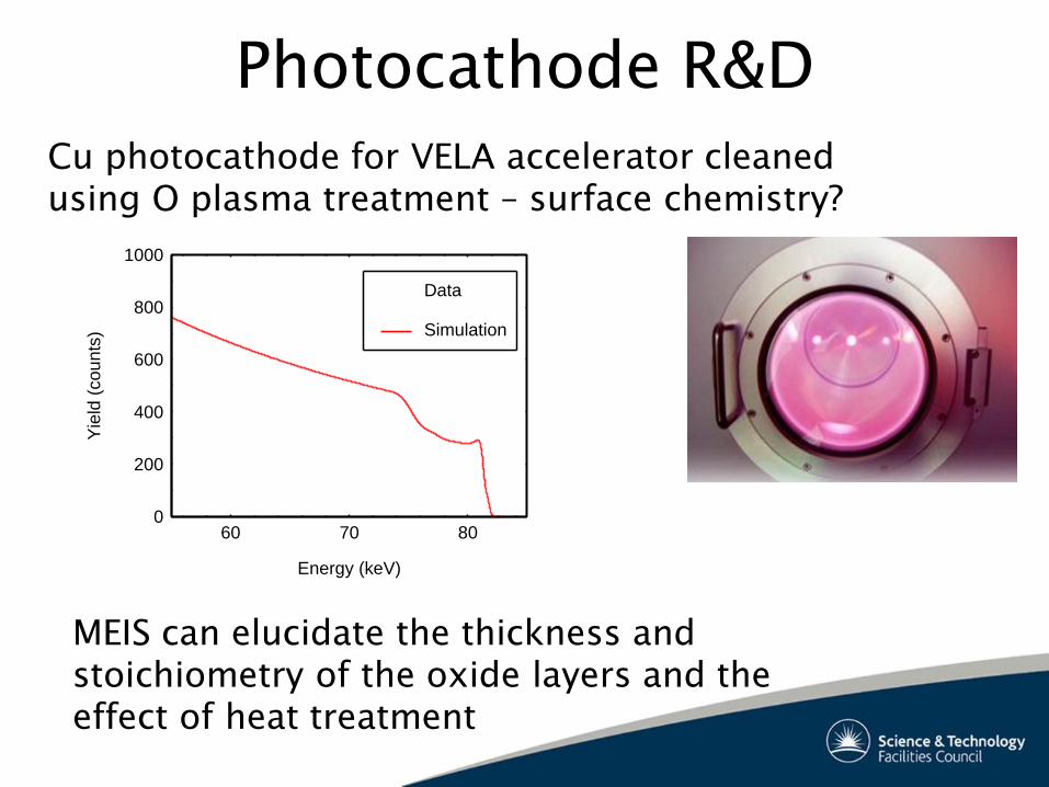
Photocathode R&D
Cu photocathode for VELA accelerator cleaned
using O plasma treatment – surface chemistry?
0
200
400
600
800
1000
60 70 80
Data
Simulation
Energy (keV)
Yie
ld (
co
un
ts)
MEIS can elucidate the thickness and
stoichiometry of the oxide layers and the
effect of heat treatment
Summary
MEIS is a fantastic technique for
investigating the surface and near-surface
region of materials
Simultaneous measurement of composition
and structure
High sensitivity to structural parameters
(~2 pm)
Virtually monolayer depth resolution
Acknowledgements
Daresbury – Paul Bailey, Kevin Connell, Steve Bennett, Graham
Bushnell-Wye, Brian Blackwell, Mark Pendleton, Paul Whitfield,
Steve Davis, Simon Letts, Vic Pucknell
York – Steve Tear, Dave Spence
Liverpool – Paul Chalker, Richard Potter, Paul Marshall, Steve
Taylor, Anthony Jones
Manchester – Peter Skeldon, George Thompson, Sergio Garcia-
Vergara
Liverpool – Ronan McGrath, Hem-Raj Sharma, Joe Smerdon, Joe
Parle, Peter Nugent
Warwick – Gavin Bell, Paul Quinn, Neil Wilson, Stuart Hatfield,
Chris McConville, Salim Al-Harthi, Faramaz Gard
St Andrews – Chris Baddeley, Andrew Haire, Johan Gustafson,
Aofie Trant, Tim Jones


