Mechanistic benefits of millisecond annealing for...
12
Mechanistic benefits of millisecond annealing for diffusion and activation of boron in silicon Charlotte T. M. Kwok, 1 Richard D. Braatz, 1 Silke Paul, 2 Wilfried Lerch, 2 and Edmund G. Seebauer 1,a 1 Department of Chemical and Biomolecular Engineering, University of Illinois, Urbana, Illinois 61801, USA 2 Mattson Thermal Products GmbH, Daimlerstrasse 10, 89160 Dornstadt, Germany Received 17 October 2008; accepted 5 January 2009; published online 19 March 2009 Millisecond annealing techniques with flash lamps or lasers have become increasingly common for activating dopants and eliminating implantation-induced damage after ion implantation for transistor junction formation in silicon. Empirical data show that such techniques confer significant benefits, but key physical mechanisms underlying these benefits are not well understood. The present work employs numerical simulation and analytical modeling to show that for boron, millisecond annealing reduces unwanted dopant spreading by greatly reducing the time for diffusion, which more than compensates for an increased concentration of Si interstitials that promote dopant spreading. Millisecond annealing also favorably alters the relative balance of boron interstitial sequestration by the crystal lattice vs interstitial clusters, which leads to improved electrical activation at depths just short of the junction. © 2009 American Institute of Physics. DOI: 10.1063/1.3079524 I. INTRODUCTION The continual shrinking of transistor size in silicon- based integrated circuit fabrication technologies has imposed increasingly stringent requirements on pn junction properties such as junction depth, profile abruptness, and sheet resistance. 1 The need to incorporate high concentrations of electrically active dopant within 20 nm or less of the surface poses difficult challenges for ion implantation technology and subsequent thermal annealing. Annealing methodology has progressed over the past decade toward faster ramp rates and shorter high-temperature cycle times–from roughly 1 s in rapid thermal processing RTPRef. 2 to roughly 1 ms or less in flash 3 and laser annealing. 3 This progression has led to less dopant diffusion and improved electrical activation, es- pecially in the problematic case of boron. However, key physical mechanisms underlying these benefits are not well understood. Moreover, the relative merits of combining dif- ferent annealing programs, such as flash-assist rapid thermal processing fRTPRef. 4 or furnace annealing followed by laser irradiation, 3 also lack clear physical explanation. Progress has been made largely on an empirical basis. The present work uses a combination of numerical simulation and analytical modeling to develop a physical picture that explains the origin of the benefits conferred by millisecond annealing of boron implanted into silicon. Numerical simulations have long been used to quantify the effects of annealing on the elementary kinetic steps that compose the boron diffusion/reaction network. However, the network contains so many steps and is so complicated that a focused physical understanding of key phenomena is difficult to discern based solely upon simulation results. A complete kinetic description that incorporates all reacting species such as interstitial clusters of many sizes and stoichiom- etries leads to a model containing many dozens of activation energies and pre-exponential factors, most of which cannot be measured directly or obtained reliably from quantum cal- culations. The parameters within such a simulation model are therefore typically obtained via fitting large experimental data sets together with making artful presuppositions about the reasonability of the parameters. Such an approach can yield accurate correlation models within the domain of ex- perimental data but casts doubt upon subsequent physical interpretation. Some recent work has pursued a different approach that simplifies the kinetic description by dramatically reducing the number of rate equations but simultaneously choosing the remaining equations to capture the key elements of a restricted set of phenomena. Corresponding rate parameters are estimated through Bayesian statistics. For example, de- scriptions have emerged 5 that incorporate a more accurate description of interstitials via surface dangling bonds 6,7 and the effects of near-surface band bending. 8 The present work employs such an approach for boron. Simulations are em- ployed to estimate the spatial and temporal variation in boron and silicon interstitial atoms during spike and flash anneal- ing, and those values are subsequently incorporated into eas- ily interpreted analytical kinetic expressions that describe the salient features of dopant diffusion and activation. II. EXPERIMENTAL METHODS To develop the simulation model for use over an ad- equately broad set of annealing regimes, a kinetic parameter set was developed from experimental data for the diffusion and activation of implanted boron via three standard proto- cols: soak annealing over many minutes, spike annealing of a Author to whom correspondence should be addressed. Electronic mail: [email protected]. JOURNAL OF APPLIED PHYSICS 105, 063514 2009 0021-8979/2009/1056/063514/12/$25.00 © 2009 American Institute of Physics 105, 063514-1 Downloaded 31 Jan 2011 to 192.17.145.40. Redistribution subject to AIP license or copyright; see http://jap.aip.org/about/rights_and_permissions
Transcript of Mechanistic benefits of millisecond annealing for...

Mechanistic benefits of millisecond annealing for diffusion and activationof boron in silicon
Charlotte T. M. Kwok,1 Richard D. Braatz,1 Silke Paul,2 Wilfried Lerch,2 andEdmund G. Seebauer1,a�
1Department of Chemical and Biomolecular Engineering, University of Illinois, Urbana,Illinois 61801, USA2Mattson Thermal Products GmbH, Daimlerstrasse 10, 89160 Dornstadt, Germany
�Received 17 October 2008; accepted 5 January 2009; published online 19 March 2009�
Millisecond annealing techniques with flash lamps or lasers have become increasingly common foractivating dopants and eliminating implantation-induced damage after ion implantation for transistorjunction formation in silicon. Empirical data show that such techniques confer significant benefits,but key physical mechanisms underlying these benefits are not well understood. The present workemploys numerical simulation and analytical modeling to show that for boron, millisecondannealing reduces unwanted dopant spreading by greatly reducing the time for diffusion, whichmore than compensates for an increased concentration of Si interstitials that promote dopantspreading. Millisecond annealing also favorably alters the relative balance of boron interstitialsequestration by the crystal lattice vs interstitial clusters, which leads to improved electricalactivation at depths just short of the junction. © 2009 American Institute of Physics.�DOI: 10.1063/1.3079524�
I. INTRODUCTION
The continual shrinking of transistor size in silicon-based integrated circuit fabrication technologies has imposedincreasingly stringent requirements on pn junction propertiessuch as junction depth, profile abruptness, and sheetresistance.1 The need to incorporate high concentrations ofelectrically active dopant within 20 nm or less of the surfaceposes difficult challenges for ion implantation technologyand subsequent thermal annealing. Annealing methodologyhas progressed over the past decade toward faster ramp ratesand shorter high-temperature cycle times–from roughly 1 sin rapid thermal processing �RTP� �Ref. 2� to roughly 1 ms orless in flash3 and laser annealing.3 This progression has led toless dopant diffusion and improved electrical activation, es-pecially in the problematic case of boron. However, keyphysical mechanisms underlying these benefits are not wellunderstood. Moreover, the relative merits of combining dif-ferent annealing programs, such as flash-assist rapid thermalprocessing �fRTP� �Ref. 4� or furnace annealing followed bylaser irradiation,3 also lack clear physical explanation.Progress has been made largely on an empirical basis. Thepresent work uses a combination of numerical simulationand analytical modeling to develop a physical picture thatexplains the origin of the benefits conferred by millisecondannealing of boron implanted into silicon.
Numerical simulations have long been used to quantifythe effects of annealing on the elementary kinetic steps thatcompose the boron diffusion/reaction network. However, thenetwork contains so many steps and is so complicated that afocused physical understanding of key phenomena is difficultto discern based solely upon simulation results. A complete
kinetic description that incorporates all reacting species�such as interstitial clusters of many sizes and stoichiom-etries� leads to a model containing many dozens of activationenergies and pre-exponential factors, most of which cannotbe measured directly or obtained reliably from quantum cal-culations. The parameters within such a simulation model aretherefore typically obtained via fitting large experimentaldata sets together with making artful presuppositions aboutthe reasonability of the parameters. Such an approach canyield accurate correlation models within the domain of ex-perimental data but casts doubt upon subsequent physicalinterpretation.
Some recent work has pursued a different approach thatsimplifies the kinetic description by dramatically reducingthe number of rate equations but simultaneously choosingthe remaining equations to capture the key elements of arestricted set of phenomena. Corresponding rate parametersare estimated through Bayesian statistics. For example, de-scriptions have emerged5 that incorporate a more accuratedescription of interstitials via surface dangling bonds6,7 andthe effects of near-surface band bending.8 The present workemploys such an approach for boron. Simulations are em-ployed to estimate the spatial and temporal variation in boronand silicon interstitial atoms during spike and flash anneal-ing, and those values are subsequently incorporated into eas-ily interpreted analytical kinetic expressions that describe thesalient features of dopant diffusion and activation.
II. EXPERIMENTAL METHODS
To develop the simulation model for use over an ad-equately broad set of annealing regimes, a kinetic parameterset was developed from experimental data for the diffusionand activation of implanted boron via three standard proto-cols: soak annealing over many minutes, spike annealing of
a�Author to whom correspondence should be addressed. Electronic mail:[email protected].
JOURNAL OF APPLIED PHYSICS 105, 063514 �2009�
0021-8979/2009/105�6�/063514/12/$25.00 © 2009 American Institute of Physics105, 063514-1
Downloaded 31 Jan 2011 to 192.17.145.40. Redistribution subject to AIP license or copyright; see http://jap.aip.org/about/rights_and_permissions

about 1 s, and millisecond �flash� annealing of about 1 ms.Details of experimental methods for soak and spike anneal-ing have already been detailed in Ref. 5, but the key featureswere as follows. For soak annealing, n-type Si�100� speci-mens about 1.5 cm�1 cm implanted with boron at 2 keVand a dose of 1�1015 ions /cm2 were cut from conventionalwafers and mounted between Ta clips for resistive heating.Heating was performed9,10 in a turbomolecularly pumpedhigh vacuum chamber with a working pressure in the low10−8 torr range. Samples were annealed at 900 °C for 1 h.Spike and flash annealing4 employed n-type Si �100� wafersimplanted with boron at 0.5 keV with a dose of 1�1015 ions /cm2. Before implantation, the native oxide wasremoved by wet-chemical etching in HF �49%�:H2O solu-tion. Spike annealing was performed in a Mattson RTP sys-tem with a maximum temperature of 1000 °C–1050 °C.Flash annealing was performed with a peak temperature of1256 °C–1322 °C. Typical temperature programs for spikeand flash annealing are shown in Figs. 1 and 2, respectively.The gaseous ambient for both spike and flash annealing wasN2 at 1 atm incorporating 100 ppm partial pressure of O2.
Characterization of soak-annealed samples was per-formed at the University of Illinois. Concentration profileswere measured ex situ by secondary ion mass spectroscopy�SIMS� using a CAMECA IMS-5f instrument. Sheet resis-tance was measured by a standard four-point probe. Thespike and flash annealed samples were analyzed at Mattson,with profiles measured ex situ by SIMS on a FEI SIMS 4600quadrupole depth profiler. For dopant activation, full-wafer
sheet resistance mapping was performed by a KLA TencorRS100.
III. MODEL FORMULATION
The boron diffusion model is based on an earlierversion5 and has been implemented by the profile simulatorFLOOPS 2000.11 The model represents boron diffusionwithin crystalline silicon, with no special provision forpreamorphizing implantation. Yet most spike and flash an-nealing technology employ a brief preheating step before themain temperature ramp. Considerable solid phase epitaxialregrowth of the amorphized layer to reform crystalline Sitypically occurs during preheating. Although regrowth doesnot always proceed to completion and boron diffusion/activation behavior can differ in details from cases whenpreamorphization is not used,12 the model may still apply inmany respects depending upon the exact processing protocol.
The model utilizes continuum equations to describe thereaction and diffusion of boron interstitial atoms and relateddefects in silicon. These equations have the general form forspecies i:
�Ci
�t= −
�Ji
�x+ Gi, �1�
where Ci, Ji, and Gi denote the concentration, flux, and netgeneration rate of species i, respectively. The flux Ji consistsof Fickian term and electric drift motion. The net generationGi incorporates terms associated with cluster formation/dissociation and kick-in/kick-out reactions between intersti-tials and the lattice through the formation of a boron-interstitial complex,13
Bs + Sii �kdis
kassoc,B
�Bs − Sii��kki
kko
Bi + Sis. �2�
The reactions for the clustering of interstitials for pure Si andmixed B-Si clusters are
BnSim−1 + Sii �kdisso
kassoc,Si
BnSim, �3�
Bn−1Sim + Bi �kdisso
kassoc,B
BnSim, n + m � 8, �4�
where the index of m and n denote the number of silicon andboron interstitials in the cluster, respectively. The maximumcluster size was set to eight, with the eight-atom dissociationenergy equated to that for very large clusters.14
The effectiveness of the surface in removing boron andsilicon interstitials was quantified by the surface annihilationprobabilities,15 SB and SSi respectively, which are incorpo-rated in the model boundary condition as
− Dk� �Ck
�x�
x=0= Jtotal,kSk, where k = Sii,Bi. �5�
Here, Jtotal denotes the total impinging flux of interstitials.The actual flux at the surface is the product of the total im-pinging flux and the surface loss probability.
FIG. 1. Temperature trajectory for spike annealing with a peak temperatureof 1050 °C.
FIG. 2. Annealing program for flash anneal experiment with a peak tem-perature of 1322 °C. Inset shows temperature trajectory during main flash.
063514-2 Kwok et al. J. Appl. Phys. 105, 063514 �2009�
Downloaded 31 Jan 2011 to 192.17.145.40. Redistribution subject to AIP license or copyright; see http://jap.aip.org/about/rights_and_permissions

Importantly, the present simulations incorporated near-surface band bending8 for spike and flash annealing but notfor soak annealing because the soak annealing time wasmuch longer than the time required to anneal out theimplantation-induced electrically active defects at the nativeoxide interface.16 Detailed reasoning can be found in Ref. 5.For spike and flash annealing, band bending was incorpo-rated by setting the surface Fermi level at 0.4 eV above thevalance band edge, in accord with the experimental value.16
That is, the potential � at the surface was represented by theboundary condition
�x=0 = Ev�T�/q + 0.4 eV/q . �6�
A priori estimates of the kinetic parameters that governthe diffusion and reaction of boron have been determinedpreviously5 by maximum likelihood �ML� estimation13,14
and maximum a posteriori �MAP� estimation17,18 which
optimally combine a variety of experimental and computa-tional data.7 Table I summarizes the a priori estimates andthe associated standard deviations. This a priori parameterset has proven capable of accurately simulating profiles forsoak and spike annealing,5 as Fig. 3�a� shows for examplesof spike annealing at 1000 °C and 1050 °C.
However, initial simulations showed that the a prioriparameters gave poor agreement with experimental profilesfor flash annealing. As shown in Fig. 3�b�, the model failedto capture the shape of the annealed profile. Moreover, thetemperature dependence of profile spreading was poorly re-produced. The simulated profiles for 1256 °C and 1322 °Calmost overlap with each other, whereas a significant differ-ence in profile shape is observed experimentally. The dis-crepancy between experiment and simulation for flash an-nealing motivated further model refinement in this regime ofsignificantly higher temperatures and shorter times. The re-finement utilized parameter sensitivity analysis and MAP es-timation.
TABLE I. A priori model parameters and confidence intervals.
Parameter Unit Value Standard deviation
95%confidence
intervalhalf-width Method Ref
1. Cluster dissociation–pure Si cluster
E2 �size 2� eV 1.400 0.030 0.060 ML 14E3 �size 3� eV 1.796 a a a a
E4 �size 4� eV 2.192 a a a a
E5 �size 5� eV 2.588 a a a a
E6 �size 6� eV 2.983 a a a a
E7 �size 7� eV 3.379 a a a a
E8=Elarge �large� eV 3.775 0.003 0.013 MAP 18
2. Cluster dissociation–pure B cluster
E2,B �size 2� eV 1.788 0.012 0.024 MAP 17
3. Cluster dissociation–mixed B-Si cluster
E3,mix �size 3� eV 1.750 a a a a
E4,mix �size 4� eV 2.100 a a a a
E5,mix �size 5� eV 2.450 a a a a
E6,mix �size 6� eV 2.800 a a a a
E7,mix �size 7� eV 3.150 a a a a
E8,mix=Elarge,mix �large� eV 3.500 b b ML 14
4. Kick-in/kick-out reactionEko eV 0.408 0.008 0.015 MAP 17Eki eV 0.458 0.008 0.015 MAP 17Edis eV 0.575 0.002 0.004 MAP 17
5. Interstitial diffusionEdiff,Si eV 0.764 0.003 0.012 MAP 18Ediff,B eV 0.359 0.004 0.008 MAP 17
6. Surface annihilation of interstitialsSSii
- 2.5�10−5 c c c 54SBi
- 2.5�10−5 c c c 54
aDissociation energies of intermediate clusters were determined by linear interpolations of ML /MAP estimates.bML estimation was based on only a single published value.cValue of surface annihilation probabilities set based on experimental data in Ref. 19.
063514-3 Kwok et al. J. Appl. Phys. 105, 063514 �2009�
Downloaded 31 Jan 2011 to 192.17.145.40. Redistribution subject to AIP license or copyright; see http://jap.aip.org/about/rights_and_permissions

IV. METHODS FOR IMPROVED PARAMETERESTIMATION
A. Parameter sensitivity analysis
Parameter sensitivity analysis quantifies the influence ofperturbations in model parameters on the model outputs andhas been widely applied in analysis and design of chemicalsystems.20,21 The analysis determines which model param-eters need to be estimated or calculated most accurately forthe purpose at hand and which parameters can be largelyignored.
Sensitivity analysis has been applied to the activationenergies of elementary kinetic steps governing diffusion ofimplanted isotopic silicon18 during soak annealing and ofboron14 during spike annealing. The present study of boron isbased on a model5 that has advanced considerably over thatemployed in Ref. 14, however, both in sophistication of thephysics as well as the domain of relevant temperatures.These changes warranted that the sensitivity analysis be re-constructed, albeit with the focus still upon profile spreadingand dopant activation.
Sensitivity analysis requires the formulation of a matrixF of sensitivity coefficients that includes the partial deriva-tives of the variables �k with respect to the dependent vari-ables Pj,
22
Fj,k = F�Pj;�k� =�Pj��k�
��k, �7�
where F�Pj ;�k� denotes the sensitivity coefficient of the jthmeasurement to the kth parameter. Since the numerical val-ues of surface annihilation probability, S, and the variousactivation energies differ by five orders of magnitude �seeTable I�, the sensitivities are normalized to allow a moredirect comparison of the relative importance of these param-
eters. The matrix F̂ of normalized sensitivity coefficients isdefined as,23
F̂j,k = F̂�Pj;�k� =�Pj��k�� ln �k
= �k�Pj��k�
��k. �8�
In this work, the sensitivity coefficients were estimated bythe finite difference method:
F̂�Pj;�k� � �k�Pj
��k= �k�Pj��k + ��k� − Pj��k − ��k�
2��k� .
�9�
The present analysis was aimed at the sensitivity of modelparameters to metrics describing profile spreading and dop-ant activation. For profile spreading, the total sensitivity forthe kth parameter, �k
Profile, is given by the sum of squares of
the sensitivity coefficients F̂ over the entire depth of theboron profile,
�kProfile =
p=1
Nd �Cp,�k+��k− Cp,�k−��k
2��k/�k�2
, �10�
where Nd denotes the total number of data points in the bo-ron profile, and ��k /�k=0.1. The parametric sensitivity co-efficient for dopant activation �k
Rs can be determined simi-larly,
�kRs = �Rs,�k+��k
− Rs,�k−��k
2��k/�k�2
, �11�
The value of sheet resistance Rs is related to the active dop-ant concentration Cs by24
Rs =1
q0
xj
��x�Cs�x�dx
, �12�
where q and � are the electron charge and the majoritycharge carrier mobility, respectively. The junction depth xj iscalculated at �B�=5�1018 cm−3.
B. MAP estimation
MAP estimation determines the most likely values ofparameters when prior information is available.25,26 MAP es-timation optimally combines prior statistical information ofthe parameter estimates with additional experimental data toobtain improved a posteriori estimates. For the present case,prior information about the parameters13,14,17,18 already existsfrom ML estimation and MAP estimation based on densityfunctional theory calculations, isolated experiments from theliterature, and previous experiments performed in the Uni-
FIG. 3. Experimental and simulated boron profiles using a priori parameterestimates for �a� spike annealing to 1000 °C and 1050 °C and �b� flashannealing to 1256 °C and 1322 °C. The flash annealing simulations essen-tially overlay each other and are indistinguishable from each other, in con-trast to the experimental profiles.
063514-4 Kwok et al. J. Appl. Phys. 105, 063514 �2009�
Downloaded 31 Jan 2011 to 192.17.145.40. Redistribution subject to AIP license or copyright; see http://jap.aip.org/about/rights_and_permissions

versity of Illinois laboratory on boron and silicon diffusion.Table I shows these a priori estimates. Reported experimen-tal data include experimental soak-, spike-, and flash-annealed boron concentration profiles obtained as describedabove.
Details of the formulation of MAP estimation have beenprovided in Refs. 17 and 18. In brief, MAP estimation can beequivalently posed as a minimization problem,
min�
j=1,¯,d
��� − ��TV�−1�� − ��
+ j=1
d
�Y j − Pj����TV�,j−1�Y j − Pj����� , �13�
where � denotes the vector of estimated parameters, � thevector of corresponding a priori parameter estimates, V� theprior parameter covariance matrix, d the total number of an-neal experiments, Y j the vector of experimental observations,and Pj the vector of model predictions. The measurementcovariance matrix for the jth experimental data, V�,j, wasestimated previously15 by the measurement of n differentSIMS profiles on the same specimen.
For computational efficiency, the elements within � arechosen to exclude activation energies to which the model haslittle sensitivity �based on the results of sensitivity analysis�.A hyperellipsoidal confidence region quantifies the uncer-tainty in the estimates via the relation
E� = �:�� − �true�V��−1�� − �true� �
2�p�� , �14�
where denotes the confidence level, denotes the chi-squared distribution with p degrees of freedom, and V�� isthe covariance of ���−�true� estimated by
cov��� − �true� = V�� � �FT�V�,1 0 0
0 � 0
0 0 V�,d�
−1
F
+ �V�−1 0
0 0��
−1
, �15�
where �� and �true denote the best estimate and the true valueof the vector of parameters, respectively, and each 0 is amatrix of zeros of compatible dimensions. The matrix F isthe sensitivity matrix of the vector of model predictions,
P = �P1, ¯ ,Pd�T �16�
with respect to the vector of parameters �, computed fromEq. �7�. The hyperellipsoidal confidence region can be visu-alized by approximate confidence intervals:27
�k� − �
2�p�V��,kk � �true,k � �k� + �
2�p�V��,kk �17�
V. RESULTS AND DISCUSSION
A. Parameter sensitivity analysis
Table II shows values of the sensitivity coefficients forprofile spreading and sheet resistance for soak, spike, and
flash annealing. Comparisons among coefficients can bemade validly only for coefficients within a given group �i.e.,in the same column�. The absolute magnitudes of the coeffi-cients may be useful for some purposes, but this work con-cerns itself with the relative magnitudes. The results forspike annealing agree qualitatively with a previous sensitiv-ity analysis for spike annealing that employed an earlier andmore primitive version of the model.14 The most influentialactivation energies are those for interstitial boron diffusion,dissociation of large clusters, dopant kick-in reaction, anddissociation of the �B-Si� complex to liberate either intersti-tial B �kick-out� or Si.
The coefficients in Table II show that the major differ-ence in the sensitivity results among the three annealing re-gimes lies in the increased relative importance of the disso-ciation energies for the B-Si mixed clusters as time scaleincreases �and maximum temperature decreases�, particularlyfor the largest mixed cluster, Elarge,mix. The sensitivity coef-ficient for this parameter is more than one order of magni-tude higher than that for boron diffusion and kick-in/kick-outreactions in soak annealing but is one order of magnitudelower in flash annealing.
The sensitivity of the dissociation energy of the secondlargest Si-B cluster, E7,mix, is higher than that of Elarge,mix forflash annealing, but the opposite trend is observed for soakand spike annealing. This decreased importance of Elarge,mix
can be explained by retarded dissociation of large clusterswhen the time scale decreases �or equivalently, when theramp rate increases�. It has been shown previously28 that at agiven temperature T, the dissociation energy E� of the mostactively dissociating clusters depends upon the ramp rate �according to
�E�/kT −1
2�exp�E�/kT −
1
2� = AdissoT/� , �18�
where Adisso is the pre-exponential factor for cluster dissocia-tion. For flash annealing, substituting T=1595 K �1322 °C,a typical maximum in flash processing� and the experimentalramp-up rate of �=2�105 °C /s gives E�=3.02 eV, whichis within 10% �i.e., �� /� in Eq. �10�� of E7,mix �3.15 eV�.Therefore, the next-to-largest clusters are dissociating, butthe largest clusters �Elarge,mix=3.5 eV� have not yet dissoci-ated at the peak temperature for flash annealing. For spikeannealing, substituting T=1323 K �1050 °C, a typical maxi-mum in spike processing� and the experimental ramp-up rateof �=168 °C /s gives E�=3.27 eV, which is above E7,mix
and within 10% of Elarge,mix. Thus, the next-to-largest clustershave already largely dissociated, and the largest clustersdominate most dissociation activity. For the case of soakannealing, the dissociation state of the largest clusters can beestimated by calculation of the constant-temperature timeconstant. At 900 °C, the time constant for the dissociation ofthe largest clusters equals �kdisso�−1= �Adisso exp�−3.5 /kT��−1
=185 s. For an annealing time of 1 h, the largest clusters arethe last ones to dissociate and dominate the final state of theprofile.
This calculation can explain two aspects of the results ofthe sensitivity analysis. Since the largest clusters have not yetdissociated for the case of flash annealing, the corresponding
063514-5 Kwok et al. J. Appl. Phys. 105, 063514 �2009�
Downloaded 31 Jan 2011 to 192.17.145.40. Redistribution subject to AIP license or copyright; see http://jap.aip.org/about/rights_and_permissions

sensitivity coefficient of its dissociation energy is less thanthat of the next-largest cluster �E7,mix=3.15 eV�, which isactively dissociating at the top of the flash. The oppositetrend is observed for soak and spike annealing, for which thelargest clusters dominate dissociation activity.
In addition, some of the interstitials liberated at the topof the flash can accrete onto the remaining next-largest clus-ters to form the largest size, as shown in Eqs. �3� and �4�.However, no equivalent interstitial sink exists in the simula-tion if the largest cluster is also dissociating, as in the case ofspike and soak anneals. If the largest clusters are dissociat-ing, the effect on interstitial release will be more pronouncedthan that of dissociation of intermediate clusters. This effectexplains the decreased relative importance of cluster energet-ics compared to kick-in/kick-out reactions as ramp rate in-creases. In soak annealing, Elarge,mix has the highest sensitiv-ity among all model parameters. In spike annealing, thedissociation of an intermediate size cluster �i.e., E7,mix� has asensitivity coefficient similarly large to those of the activa-tion energies for kick-in/kick-out reactions. And in flash an-nealing, the dissociation of an intermediate size cluster �i.e.,E7,mix� has lower sensitivity than the activation energies ofkick-in/kick-out reactions.
In contrast to previous work,14 the present work exam-ined the influences of pure Si clusters and mixed B-Si clus-ters separately. Table II shows that energetics of dissociationof pure Si and mixed B-Si clusters have different sensitivitycoefficients, with the dissociation energies of mixed B-Siclusters exerting more influence than those of pure Si clus-ters. This observation validates the suggestion made in a pre-vious silicon self-diffusion study18 that the standard devia-tion for pure Si cluster energetics is underestimated bysetting sensitivities equal for pure Si and mixed B-Si clus-ters.
The total sensitivities for the surface annihilation prob-ability S are low compared to the clustering and kick-in/kick-out energetics. However, note that the present sensitivityanalysis quantifies the change in boron profile upon a pertur-bation of only 10% in the model parameter. Although thesensitivity coefficient for the surface annihilation probabilityis rather small for the specific value chosen here, that situa-tion could change under other circumstances. In contrast toactivation energies in the model, the surface annihilationprobability can vary �sometimes controllably� by several or-ders of magnitude depending on surface conditions.7,18
Hence, it would be incorrect to conclude based upon the
TABLE II. Sensitivity coefficients for profile spreading and sheet resistance.
Profile sensitivity �Profile �cm−3�2 Resistance sensitivity �Rs �� /sq�2
Parameter Soak Spike Flash Soak Spike Flash
1. Cluster dissociation–pure Si clusters
E2 1.1�1035 1.2�1039 8.9�1038 7.8�10 1.6�10 1.4�10−3
E3 1.9�1038 3.5�1040 7.9�1040 1.3�102 1.3�10 1.6E4 3.7�1037 2.3�1039 2.4�1039 1.4�103 3.8�102 2.5�10−1
E5 1.3�1038 7.7�1039 8.0�1040 3.4�103 2.0�103 8.7�10−1
E6 4.7�1037 3.1�1040 2.8�1041 5.4�102 3.9�102 3.5�10−1
E7 4.1�1035 3.8�1037 1.3�1039 6.0�10−1 1.7�10−1 1.1�10−3
Elarge 7.6�1035 4.6�1038 1.6�1038 3.6�10−1 7.1�10−4 5.6�10−5
2. Cluster dissociation–pure B clusters
E2,B 1.8�1038 4.0�1042 7.1�1042 2.6�104 7.4�103 8.8�10−2
3. Cluster dissociation–mixed B-Si clustersE3,mix 4.1�1038 1.7�1042 1.1�1042 1.2�104 1.1�103 1.1E4,mix 3.1�1037 6.3�1039 3.6�1041 4.8�103 8.8�102 1.5�10−1
E5,mix 1.4�1040 4.0�1041 1.8�1042 6.8�103 8.5�102 1.5�10E6,mix 2.5�1042 9.2�1042 4.9�1042 1.2�104 2.0�104 2.3�103
E7,mix 1.2�1043 3.3�1043 9.7�1042 1.8�104 1.0�105 1.2�104
Elarge,mix 4.4�1043 1.0�1044 1.0�1042 6.6�104 2.9�106 4.3�105
4. Kick-in/kick-out reaction
Eko 7.8�1041 1.2�1044 9.7�1043 1.6�106 8.9�105 3.6�102
Eki 9.9�1041 1.5�1044 1.2�1044 2.0�106 1.1�106 4.8�102
Edis 1.6�1042 3.9�1043 4.3�1043 2.0�106 1.2�106 4.3�102
5. Interstitial diffusion
Ediff,Si 2.8�1034 3.8�1038 2.9�1040 9.1 7.9 1.3�10−5
Ediff,B 6.2�1041 1.4�1043 9.5�1042 8.1�105 4.8�105 1.5�102
6. Surface annihilation of interstitials
SSii6.5�1039 1.2�1040 6.2�1037 5.59�10−3 2.20�10 3.1
SBi1.1�1038 1.7�1039 9.7�1037 3.53�10−1 1.14�10 8.1
063514-6 Kwok et al. J. Appl. Phys. 105, 063514 �2009�
Downloaded 31 Jan 2011 to 192.17.145.40. Redistribution subject to AIP license or copyright; see http://jap.aip.org/about/rights_and_permissions
sensitivities in Table II that surface interstitial annihilationcannot exert strong effects on boron diffusion and activation.
For the three annealing regimes studied, parameters thatmatter most in profile spreading are also important in dopantactivation. This suggests that dopant diffusion and activationare highly correlated, which is consistent with the well-known trade-off relation observed experimentally betweenjunction depth and sheet resistance.29
B. MAP estimation
Based on the results of parameter sensitivity analysis,the vector of parameters for MAP estimation was formulatedto include the four most influential parameters from each ofthe soak, spike, and flash annealing protocols. The vectorwas also set to include the corresponding surface loss prob-abilities,
�T = �E6,mix,E7,mix,Elarge,mix,Eko,Eki,Edis,Ssoak,Sspike,Sflash� .
�19�
Even though the sensitivity coefficients for S are rather lowunder present conditions, the database for values of S is verysmall. The present analysis is capable of adding to that data-base. The soak annealing experiments employed a differentsurface treatment from the spike and flash experiments, andS can vary significantly with even small changes in thechemical state of the surface.7 S is also believed to vary�rather weakly� with temperature on Si�100�.30 As the maxi-mum temperatures vary by more than 400 °C in these ex-periments, changes in S may occur. The present work as-sumes equal surface loss probabilities for boron and siliconinterstitials, SBi
=SSii. The annihilation probabilities could in
principle differ for Si and B. However, as of yet there isinsufficient scientific understanding to predict the magnitudeof such a difference, and the present model sought to mini-mize the number of independently variable parameters.
Table III shows the MAP estimates of the model param-eters and the associated 95% confidence intervals. Figure 4shows examples of experimental and simulated profiles usingthe refined estimates. Values of sheet resistance are also in-cluded. There is significant improvement in profile fit afterMAP estimation for the flash annealed profile, with the goodagreement in soak and spike annealing utilizing a priori es-timates retained.
Figure 5 shows the trade-off relation between sheet re-sistance and junction depth for both spike and flash anneal-ing. Figure 5 also shows corresponding experimental data
FIG. 4. Experimental and simulated boron profiles with refined MAP pa-rameter estimates for �a� soak annealing at 900 °C, �b� spike annealing at1000 °C, �c� spike annealing at 1050 °C, �d� flash annealing at 1256 °C,�e� flash annealing at 1278 °C, and �f� flash annealing at 1322 °C. Fits aregood over the entire range of conditions.
TABLE III. Refined MAP estimates and confidence intervals.
Parameter MAP estimateStandarddeviation
95% confidenceinterval half-width
E6,mix 2.729 0.008 0.034E7,mix 2.960 0.003 0.014Elarge,mix 3.697 0.003 0.011Eko 0.411 0.002 0.007Eki 0.464 0.002 0.007Edis 0.574 0.001 0.005Ssoak 5.180�10−5 2.296�10−6 8.612�10−6
Sspike 4.476�10−5 2.417�10−6 9.065�10−6
Sflash 7.915�10−5 3.690�10−6 1.384�10−5
063514-7 Kwok et al. J. Appl. Phys. 105, 063514 �2009�
Downloaded 31 Jan 2011 to 192.17.145.40. Redistribution subject to AIP license or copyright; see http://jap.aip.org/about/rights_and_permissions

from spike29,31–38 and flash39,40 annealing that have been ex-tracted from the literature. The model output agrees wellwith the experimental trend for both annealing schemes andconfirms the simultaneous improvement in dopant activationand junction depth characteristic of flash annealing.
All of the experimental MAP parameter estimates liewithin the a priori confidence intervals shown in Table I.Thus, these MAP estimates lie within the expected distancesof the prior estimates but have substantially smaller standarddeviations. Since the various model parameters exert differ-ent sensitivities in different annealing methods, incorporationof the broader range of experimental data having widely di-vergent time scales and peak temperatures served to imposetight constraints on the values of parameters and thereby im-prove the accuracy of the estimates.
The value of S for flash annealing is about a factor of 1.5higher than that for soak and spike annealing. The differencemay originate from differences in surface conditions �evensubtle� due to processing protocols and possibly in process-ing temperature. However, the values of S for all three meth-ods are much smaller than the maximum value of �0.05�Ref. 6� measured for an atomically clean, chemically activeSi�100� surface. The small values in the present experimentsprobably arise from oxygen in the processing environment.
C. Effects of annealing protocol on borondiffusion
The model and parameter set have demonstrated theircapability to simulate key aspects of boron diffusion andactivation over a maximum temperature range greater than400 degrees wide �from 900 °C to 1322 °C� and more than
six orders of magnitude in time scales �from �1 ms to 1 h�.Such a broad range of applicability offers confidence that themodel reproduces interstitial concentrations accuratelyenough to serve as the input for an analytical description ofthe primary mechanisms governing boron diffusion and acti-vation during the transient heating characteristic of spike andmillisecond annealing.
An analytical expression to rationalize the effects oframp rate on boron profile spreading near the junction duringspike annealing has been developed previously.28,42 The ex-pression was based on the simple random-walk diffusionequation Xlattice
2 =6Dt, with Xlattice being the mean square dis-placement of diffusing dopant interstitials that sometimes ex-change with the lattice, and t being a characteristic diffusiontime. The following expression was derived for Xlattice:
Xlattice2 = 6 2kassoc�Sii�tmax
�exp��Eki − Ediff,Bi�/kT��1 − b�/b , �20�
where denotes the site-to-site interstitial hop length of 0.27nm. The reaction constant kassoc equals 4�aDSi, wherein aand DSi denote the capture radius and the diffusivity of sili-con interstitials, respectively. The time tmax represents a char-acteristic time span over which the wafer remains near thepeak temperature �within 95% of the peak�, and �Sii� denotesthe concentration of Si interstitials at the peak temperature,which is given by the simulation model. The variable b rep-resents the branching ratio between the dissociation reactionof the Bs–Sii complex to form either Bi or Sii. Assuming thatthe rate constants for these two reactions share the value forthe same pre-exponential factor A, the branching ratio can beexpressed as
b =A exp�− Edis/kT�
A exp�− Edis/kT� + A exp�− Eko/kT�
=1
1 + exp�Edis − Eko
kT� . �21�
With the a priori parameter set from Ref. 17, Eq. �20�showed28 good agreement �within 10%–20%� with experi-mental spreading profiles for spike annealing over the rela-tively limited range of conditions examined. With the presentrefined MAP parameter estimates, Eq. �20� should yield goodagreement with the experimental spreading observed over amuch broader temperature range. Indeed, Eq. �20� estimatesprofile spreading �at �B�=5�1018 cm−3� of 20.6 nm and 4.8nm for spike �1050 °C� and flash �1322 °C� annealing, re-spectively. These analytical estimates agree exceptionallywell with the experimental observations of 21.6 nm and 4.7nm.
The relatively simple form of Eq. �20� permits clear in-sights into the differing effects of spike and millisecond an-nealing on boron diffusion. Table IV shows key quantitiescomposing Eq. �20� calculated for the particular experimen-tal conditions described in this work but also representativeof conditions typically employed in these annealing proto-cols. The major difference between the two methods lies inthe values of kassoc�Sii� and tmax. As discussed in Ref. 28,
FIG. 5. Relation between sheet resistance and junction depth �at �B�=5�1018 cm−3� for spike and flash anneals. Experimental data for spike an-nealing �Refs. 29 and 31–38� include results for implanted B and BF2 an-nealed with peak temperatures of 1000–1050 °C �implant conditions: B:0.2–2 keV, 5�1014–2�1015 cm−2; BF2:1.1–2.2 keV, 1�1015 cm−2, with-out preamorphization�. Experimental data for flash annealing �Refs. 39 and40� include results from experiments utilizing similar implant conditionswith peak temperatures of 1256–1350 °C. Initial conditions for simulationsemploy experimental as-implanted profiles �B, 0.5–3 keV, 1�1015–2�1015 cm−2, without preamorphization� as well as simulated implantedprofiles from the Dual Pearson model �Ref. 41� �BF2, 1 keV, 5�1014–1�1015 cm−2, without PAI�. Dashed lines are guides for the eyes. Simula-tions track experimental trends quite well.
063514-8 Kwok et al. J. Appl. Phys. 105, 063514 �2009�
Downloaded 31 Jan 2011 to 192.17.145.40. Redistribution subject to AIP license or copyright; see http://jap.aip.org/about/rights_and_permissions

�kassoc�Sii��−1 represents a characteristic time for the kick-outof substitutional boron from the lattice by Si interstitials,thereby rendering the boron mobile. The combined quantitytmax�kassoc�Sii� represents the number of liberation eventsnear the temperature peak, where most dopant diffusion oc-curs. Although kassoc�Sii� is almost two orders of magnitudelarger for flash annealing than for spike annealing—owingmainly to the higher interstitial concentration—the corre-sponding time scale tmax is almost three orders of magnitudesmaller. As a result of this compensation, flash annealingreduces the profile spreading significantly.
This explanation differs from that invoked to explain thebenefits of increased ramp rate in spike annealing.42 In thatcase, a similar analysis showed that fast ramp rates �on theorder of 400 °C /s� to a fixed peak temperature reduce thetime during which the implanted profile is exposed to themaximum concentrations of Si interstitials. The fast rampalso pushes the dissociation of large interstitial clusters �withhigh dissociation energies� up to higher temperatures. For aconstant peak temperature, this dissociation “delay” duringthe ramp slightly reduces the maximum concentrations of Siinterstitials. Both the shortened exposure time and reducedinterstitial concentration inhibit dopant diffusion. In the mil-lisecond annealing, however, the peak temperature greatlyexceeds that for spike annealing. Thus, even though thefaster ramping of millisecond annealing pushes up the clusterdissociation temperatures, the maximum Si interstitial con-centrations still greatly exceed those for spike annealing. Thebenefits from millisecond annealing derive from the short-ened time scale that outweighs the effects of increased Siinterstitial concentration.
This physical picture points to even further potential re-ductions in junction depth through methods that operate oneven shorter time scales than flash annealing, such as anneal-ing with scanned continuous-wave43,44 or pulsed45,46 lasers.However, the effects of very fast methods on dopant activa-tion complicate matters, as discussed further below.
D. Effects of annealing protocol on boron activation
Equation �20� also helps to explain the improved dopantactivation seen in millisecond annealing, although the analy-sis must be applied in a spatially dependent way. When clus-ters dissociate to release boron interstitial atoms, those inter-stitials diffuse until sequestered either by kick-in to the
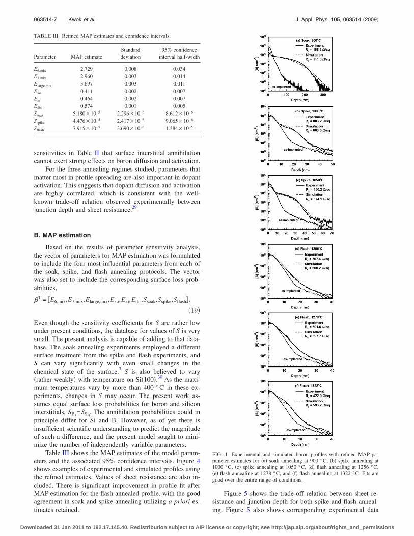
lattice �Eq. �2�� or by reaccretion back into remaining clus-ters �Eq. �4��. Sequestration by the lattice leads to electricallyactive boron that remains largely immobile but electricallyactive until a Si interstitial arrives to drive a kick-out reac-tion. Equation �20� gives the typical distance that a typicalboron atom released from a cluster will move during theannealing cycle if this sequestration mechanism dominates.Because �Sii� varies with depth into the wafer due to varyingconcentrations of clusters, Xlattice also varies with depth. Fig-ure 6 shows this variation in Xlattice calculated via Eq. �20�for typical maximum temperatures in spike and flash anneal-ing. In these calculations, the values of �Sii� originated fromsimulations. In all cases, the spatial variation of Xlattice exhib-its a maximum value near the peak of the interstitial clusterconcentration at depths �5 nm and drops off to lower val-ues in directions toward the interstitial sink regions both atthe surface and in the bulk. The maximum simply reflects theincreased rate of Si interstitial creation where many clustersare dissociating. For similar reasons, Xlattice at any depth in-creases as the maximum temperature rises and induces moreclusters to dissociate.
Figure 6 also shows diffusion distances Xcluster calculatedwith the alternative assumption that sequestration of B inter-stitials into remaining clusters dominates. Typically only thelargest clusters �that have the highest dissociation energies�still exist intact at the highest annealing temperatures. Thus,the B diffusion distances limited by cluster sequestration canbe estimated as simply the average spacing between the larg-est clusters �size 8� in the model:
Xcluster = �largest clusters�−1/3. �22�
The values of Xcluster also vary with depth but in a directiongenerally opposite to Xlattice because Xlattice increases withcluster concentration while Xcluster decreases.
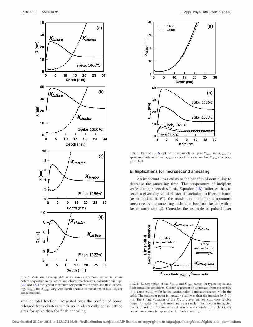
Figure 7 plots the same results as Fig. 6 but in a way thatfacilitates direct comparison of various annealing protocolsregarding the behavior of Xcluster and Xlattice. Figure 7 showsthat Xcluster remains largely invariant with annealing condi-tions, while Xlattice varies strongly. The Xlattice curves forspike annealing lie substantially above those for flash anneal-ing.
This difference among annealing protocols for Xlattice liesat the heart of the improved electrical activation performanceof flash annealing compared to spike for the following rea-son. The dominant B sequestration mode is simply themechanism that has the smallest value of X. A superpositionof the Xcluster and Xlattice curves indicates which mechanismdominates as a function of depth. Figure 8 shows schemati-cally such superposition for spike and flash annealing. Forthe typical conditions examined here, cluster sequestrationdominates from the surface to a depth xcross, while latticesequestration dominates deeper within the solid. The cross-over point is typically shallower than the junction by 5–10nm. The strong variation in the Xlattice curves with annealingconditions means that the position of xcross is considerablydeeper for spike than for flash annealing. In consequence, a
TABLE IV. Key quantities in Eq. �20� for typical conditions in spike andflash annealing.
Parameter UnitSpike anneal�1050 °C�
Flash anneal�1322 °C�
tmax s 6.3�10−1 6.3�10−4
kassoc�Sii� s 1.4�102 1.2�104
tmax�kassoc�Sii� - 88 7.6�1−b� /b - 4.2 3.3exp��Eki−Ediff,B� /kT� - 2.5 2.2X �model� nm 20.6 4.8X �expt.� nm 21.6 4.7
063514-9 Kwok et al. J. Appl. Phys. 105, 063514 �2009�
Downloaded 31 Jan 2011 to 192.17.145.40. Redistribution subject to AIP license or copyright; see http://jap.aip.org/about/rights_and_permissions
smaller total fraction �integrated over the profile� of boronreleased from clusters winds up in electrically active latticesites for spike than for flash annealing.
E. Implications for microsecond annealing
An important limit exists to the benefits of continuing todecrease the annealing time. The temperature of incipientwafer damage sets this limit. Equation �18� indicates that, toreach a given degree of cluster dissociation to liberate boron�as embodied in E��, the maximum annealing temperaturemust rise as the annealing technique becomes faster �with afaster ramp rate ��. Consider the example of pulsed laser
FIG. 6. Variation in average diffusion distances X of boron interstitial atomsbefore sequestration by lattice and cluster mechanisms, calculated via Eqs.�20� and �22� for typical maximum temperatures in spike and flash anneal-ing. Xlattice and Xcluster vary with depth because of variations in local clusterconcentrations.
FIG. 7. Data of Fig. 6 replotted to separately compare Xlattice and Xcluster forspike and flash annealing. Xcluster shows little variation, but Xlattice changes agreat deal.
FIG. 8. Superposition of the Xcluster and Xlattice curves for typical spike andflash annealing conditions. Cluster sequestration dominates from the surfaceto a depth xcross, while lattice sequestration dominates deeper within thesolid. The crossover point is typically shallower than the junction by 5–10nm. The strong variation of the Xlattice curves moves xcross considerablydeeper for spike than flash annealing, so a smaller total fraction �integratedover the profile� of boron released from clusters winds up in electricallyactive lattice sites for spike than for flash annealing.
063514-10 Kwok et al. J. Appl. Phys. 105, 063514 �2009�
Downloaded 31 Jan 2011 to 192.17.145.40. Redistribution subject to AIP license or copyright; see http://jap.aip.org/about/rights_and_permissions

annealing with a 200 ns pulse46 as compared to flash anneal-ing to 1322 °C. In flash annealing, the ramp rate is �=2�105 °C /s, compared to �=3�109 °C /s for the pulsed la-ser. For this particular flash annealing case, Eq. �18� yieldsE�=3.02 eV. For the pulsed laser process to reach the samevalue of E� �and therefore degree of initial boron releasefrom clusters�, the maximum temperature would have to in-crease vastly up to 2450 °C. This temperature is far abovethe Si melting point of 1410 °C. The limited cluster disso-ciation leads to poor dopant activation47–49 and, by relatedmechanisms, to the incomplete removal of EOR defects49–51
commonly observed in microsecond annealing.
VI. CONCLUSION
On an empirical basis, multiple continuous-wave laserbeam scans51 or multiple pulses45,46 are sometimes employedto mitigate problems with short-time annealing techniques.An alternative approach involves using two-step annealingprotocols comprising laser irradiation in conjunction withfurnace annealing3 or conventional RTP.52,53 The lowerramp-rate step dissociates clusters to improve activationwhereas the use of intermediate temperature ensures limitedprofile spreading. Design of alternatives through laser pulseduration,54 number of laser pulses, and varying combinationsof laser with furnace annealing steps or RTP can be effectedto a reasonable approximation by the sort of mathematicalanalysis given above.
ACKNOWLEDGMENTS
This work was partially supported by ACS PetroleumResearch Fund �Grant No. 43651-AC5� and NSF �Grant No.DMR 07-04354�. SIMS for the soak-annealed material wasperformed at the Center for Microanalysis of Materials, Uni-versity of Illinois, which is partially supported by the U.S.Department of Energy under Grant No. DEFG02-96-ER45439. We thank Chris Hatem of Varian SemiconductorEquipment Associates for providing the boron-implanted wa-fer used for soak annealing.
1See The International Technology Roadmap for Semiconductors, 2006Update �http://www.itrs.net/Links/2006update/2006UpdateFinal.htm�.
2T. Gebel, M. Voelskow, W. Skorupa, G. Mannino, V. Privitera, F. Priolo,E. Napolitani, and A. Carnera, Nucl. Instrum. Methods Phys. Res. B 186,287 �2002�.
3S. Baek, S. Heo, H. Choi, and H. Hwang, J. Vac. Sci. Technol. B 23, 257�2005�.
4W. Lerch, S. Paul, J. Niess, S. McCoy, T. Selinger, J. Gelpey, F. Cristiano,F. Severac, M. Gavelle, S. Boninelli, P. Pichler, and D. Bolze, Mater. Sci.Eng., B 124–125, 24 �2005�.
5C. T. M. Kwok, R. D. Braatz, S. Paul, W. Lerch, and E. G. Seebauer,AIChE J. �submitted�.
6C. T. M. Kwok, K. Dev, R. D. Braatz, and E. G. Seebauer, J. Appl. Phys.98, 013524 �2005�.
7E. G. Seebauer, K. Dev, M. Y. L. Jung, R. Vaidyanathan, C. T. M. Kwok,J. W. Ager, E. E. Haller, and R. D. Braatz, Phys. Rev. Lett. 97, 055503�2006�.
8M. Y. L. Jung, R. Gunawan, R. D. Braatz, and E. G. Seebauer, J. Appl.Phys. 95, 1134 �2004�.
9M. A. Mendicino and E. G. Seebauer, Surf. Sci. 277, 89 �1992�.10M. A. Mendicino and E. G. Seebauer, J. Electrochem. Soc. 140, 1786
�1993�.11See Mark Law, University of Florida at Gainesville, http://
www.swamp.tec.ufl.edu/
12S. H. Jain, P. B. Griffin, J. D. Plummer, S. McCoy, J. Gelpey, T. Selinger,and D. F. Downey, IEEE Trans. Electron Devices 52, 1610 �2005�.
13M. Y. L. Jung, R. Gunawan, R. D. Braatz, and E. G. Seebauer, AIChE J.50, 3248 �2004�.
14R. Gunawan, M. Y. L. Jung, R. D. Braatz, and E. G. Seebauer, J. Electro-chem. Soc. 150, G758 �2003�.
15C. T. M. Kwok, K. Dev, R. D. Braatz, and E. G. Seebauer, J. Appl. Phys.98, 013524 �2005�.
16K. Dev, M. Y. L. Jung, R. Gunawan, R. D. Braatz, and E. G. Seebauer,Phys. Rev. B 68, 195311 �2003�.
17R. Gunawan, M. Y. L. Jung, E. G. Seebauer, and R. D. Braatz, AIChE J.49, 2114 �2003�.
18C. T. M. Kwok, K. Dev, R. D. Braatz, and E. G. Seebauer, Automatica 44,2241 �2008�.
19K. Dev, C. T. M. Kwok, R. Vaidyanathan, R. D. Braatz, and E. G. See-bauer, Proceedings of the 16th International Conference on Ion Implanta-tion Technology, 2006, Vol. 866, p. 50.
20J. R. Leis, S. A. Gallagher, and M. A. Kramer, Comput. Chem. Eng. 11,409 �1987�.
21F. D. Van Voorhees and A. Terry Bahill, Proceedings of the IEEE Interna-tional Conference of Systems, Man and Cybernetics, 1995, Vol. 2, p. 971.
22R. Tomović and M. Vukobratović, General Sensitivity Theory �Elsevier,New York, 1972�.
23E. Rusli, F. Xue, T. O. Drews, P. M. Vereecken, P. Andricacos, H. Deli-gianni, R. D. Braatz, and R. C. Alkire, J. Electrochem. Soc. 154, D584�2007�.
24F. Cristiano, N. Cherkashin, P. Calvo, Y. Lamrani, X. Hebras, A. Claverie,W. Lerch, and S. Paul, Mater. Sci. Eng., B 114–115, 174 �2004�.
25J. V. Beck and K. J. Arnold, Parameter Estimation in Engineering andScience �Wiley, New York, 1977�.
26G. Sparacino, C. Tombolato, and C. Cobelli, IEEE Trans. Biomed. Eng.47, 801 �2000�.
27H. B. Matthews III, Ph.D. thesis, University of Wisconsin, Madison, 1997.28M. Y. L. Jung, R. Gunawan, R. D. Braatz, and E. G. Seebauer, J. Electro-
chem. Soc. 151, G1 �2004�.29A. J. Murrell, E. J. H. Collart, M. A. Foad, and D. Jennings, J. Vac. Sci.
Technol. B 18, 462 �2000�.30X. Zhang, M. Yu, C. T. M. Kwok, R. Vaidyanathan, R. D. Braatz, and E.
G. Seebauer, Phys. Rev. B 74, 235301 �2006�.31D. F. Downey, S. W. Falk, A. F. Bertuch, and S. D. Marcus, J. Electron.
Mater. 28, 1340 �1999�.32A. Mokhberi, P. B. Griffin, J. D. Plummer, E. Paton, S. McCoy, and K.
Elliott, IEEE Trans. Electron Devices 49, 1183 �2002�.33B. Bayha, S. Paul, W. Lerch, D. F. Downey, E. A. Arevalo, X. Hebras, and
N. Cherkashin, Proceedings of the 14th International Conference on IonImplantation Technology, 2002, p. 618.
34B. Bayha, D. Loeffelmacher, W. Lerch, D. F. Downey, and E. A. Arevalo,Proceedings of the 13th International Conference on Ion ImplantationTechnology, 2000, p. 623.
35S. C. Jain, W. Schoenmaker, R. Lindsay, P. A. Stolk, S. Decocutere, M.Willander, and H. E. Maes, J. Appl. Phys. 91, 8919 �2002�.
36A. Agarwal, H.-J. Grossmann, and A. T. Fiory, J. Electron. Mater. 28,1333 �1999�.
37S. Paul, B. Bayha, W. Lerch, C. Merkl, D. F. Downey, and E. A. Arevalo,Proceedings of the 14th International Conference on Ion ImplantationTechnology, 2002, p. 83.
38P. J. Timans, W. Lerch, S. Paul, J. Niess, T. Heulsmann, and P. Schmid,Solid State Technol. 47�5�, 35 �2004�.
39W. Skorupa, T. Gebel, R. A. Yankox, S. Paul, W. Lerch, D. F. Downey,and E. A. Arevalo, J. Electrochem. Soc. 152, G436 �2005�.
40A. Mokhberi, L. Pelaz, M. Aboy, L. Marques, J. Barbolla, E. Paton, S.McCoy, J. Ross, K. Elliott, J. Gelpey, P. B. Griffin, and J. D. Plummer,Tech. Dig. - Int. Electron Devices Meet. 2002, 879.
41K. B. Parab, S.-H. Yang, S. J. Morris, S. Tian, A. F. Tasch, D. Kamenitsa,R. Simonton, and C. Magee, J. Vac. Sci. Technol. B 14, 260 �1996�.
42M. Y. L. Jung, R. Gunawan, R. D. Braatz, and E. G. Seebauer, J. Electro-chem. Soc. 150, G838 �2003�.
43Y. I. Nissim, A. Lietoila, R. B. Gold, and J. F. Gibbons, J. Appl. Phys. 51,274 �1980�.
44P. Timans, J. Gelpey, S. McCoy, W. Lerch, and S. Paul, Mater. Res. Soc.Symp. Proc. 912, 3 �2006�.
45A. Florakis, D. Tsoukalas, I. Zergioti, K. Giannakopoulos, P. Dimitrakis,D. G. Papazoglou, G. Bennassayag, H. Bourdon, and A. Halimaoui, Nucl.
063514-11 Kwok et al. J. Appl. Phys. 105, 063514 �2009�
Downloaded 31 Jan 2011 to 192.17.145.40. Redistribution subject to AIP license or copyright; see http://jap.aip.org/about/rights_and_permissions

Instrum. Methods Phys. Res. B 253, 13 �2006�.46F. Torregrosa, C. Laviron, F. Milesi, M. Hernandez, H. Faïk, and J. Ven-
turini, Nucl. Instrum. Methods Phys. Res. B 237, 18 �2005�.47T. Ito, T. Iinuma, A. Murakoshi, H. Akutsu, K. Suguro, T. Arikado, K.
Okumura, M. Yoshioka, T. Owada, Y. Imaoka, H. Murayama, and T.Kusuda, Jpn. J. Appl. Phys. 41, 2394 �2002�.
48W. S. Yoo and K. Kang, Nucl. Instrum. Methods Phys. Res. B 237, 12�2005�.
49J. Borland, R. J. Hillard, A. Mineji, W. Krull, M. Tanjyo, and T. Walker,Solid State Technol. 49�5�, 47 �2006�.
50C. H. Poon, L. S. Tan, B. J. Cho, A. See, and M. Bhat, J. Electrochem.
Soc. 151, G80 �2004�.51J. A. Sharp, N. E. B. Cowern, R. P. Webb, K. J. Kirkby, D. Giubertoni, S.
Gennaro, M. Bersani, M. A. Foad, F. Cristiano, and P. F. Fazzini, Appl.Phys. Lett. 89, 192105 �2006�.
52S. Earles, M. Law, R. Brindos, K. Jones, S. Talwar, and S. Corcoran, IEEETrans. Electron Devices 49, 1118 �2002�.
53E. V. Monakhov, B. G. Svensson, M. K. Linnarsson, A. la Magna, M.Italia, V. Privitera, G. Fortunato, M. Cuscunà, and L. Mariucci, Appl.Phys. Lett. 87, 192109 �2005�.
54J. Venturini, M. Hernandez, G. Kerrien, C. Laviron, D. Camel, J. L. San-tailler, T. Sarnet, and J. Boulmer, Thin Solid Films 453–454, 145 �2004�.
063514-12 Kwok et al. J. Appl. Phys. 105, 063514 �2009�
Downloaded 31 Jan 2011 to 192.17.145.40. Redistribution subject to AIP license or copyright; see http://jap.aip.org/about/rights_and_permissions