Mechanical and Thermal Design Guidelines for Lidless … · Guidelines for Designing with Lidless...
64
Mechanical and Thermal Design Guidelines for Lidless Flip-Chip Packages Application Note XAPP1301 (v1.3.1) July 2, 2018
Transcript of Mechanical and Thermal Design Guidelines for Lidless … · Guidelines for Designing with Lidless...
Mechanical and Thermal Design Guidelines for Lidless Flip-Chip Packages
Application Note
XAPP1301 (v1.3.1) July 2, 2018

Guidelines for Designing with Lidless Flip-Chip Packages 2XAPP1301 (v1.3.1) July 2, 2018 www.xilinx.com
Revision HistoryThe following table shows the revision history for this document.
Date Version Revision
07/02/2018 1.3.1 Updated web description. No technical content changes.
06/08/2018 1.3Added figures, schematics, and relevant information for new devices.
Added Appendix A, Recommended Thermal Solution Installation of Xilinx FCBGA Lidless Packages.
02/28/2018 1.2Revised text and updated figures throughout document.
Minor editorial updates and clarifications.
08/22/2017 1.1 Updated figures.
01/09/2017 1.0 Initial Xilinx release.

Guidelines for Designing with Lidless Flip-Chip Packages 3XAPP1301 (v1.3.1) July 2, 2018 www.xilinx.com
Table of ContentsRevision History . . . . . . . . . . . . . . . . . . . . . . . . . . . . . . . . . . . . . . . . . . . . . . . . . . . . . . . . . . . . . . . . . . . . 2
Chapter 1: Mechanical and Thermal Design GuidelinesSummary. . . . . . . . . . . . . . . . . . . . . . . . . . . . . . . . . . . . . . . . . . . . . . . . . . . . . . . . . . . . . . . . . . . . . . . . . 4Introduction . . . . . . . . . . . . . . . . . . . . . . . . . . . . . . . . . . . . . . . . . . . . . . . . . . . . . . . . . . . . . . . . . . . . . . 5Lidless Flip-Chip Packages . . . . . . . . . . . . . . . . . . . . . . . . . . . . . . . . . . . . . . . . . . . . . . . . . . . . . . . . . . . 5Package Mechanical Specifications . . . . . . . . . . . . . . . . . . . . . . . . . . . . . . . . . . . . . . . . . . . . . . . . . . . 6Thermal Management Strategy . . . . . . . . . . . . . . . . . . . . . . . . . . . . . . . . . . . . . . . . . . . . . . . . . . . . . . 6Thermal Simulation and the Use of Thermal Models . . . . . . . . . . . . . . . . . . . . . . . . . . . . . . . . . . . . 16Example Heat Sink Thermal Performance . . . . . . . . . . . . . . . . . . . . . . . . . . . . . . . . . . . . . . . . . . . . . 32Removing Heat Sink Phase Change Material . . . . . . . . . . . . . . . . . . . . . . . . . . . . . . . . . . . . . . . . . . . 34Measurement Debug . . . . . . . . . . . . . . . . . . . . . . . . . . . . . . . . . . . . . . . . . . . . . . . . . . . . . . . . . . . . . . 36Reference Design Files . . . . . . . . . . . . . . . . . . . . . . . . . . . . . . . . . . . . . . . . . . . . . . . . . . . . . . . . . . . . . 36Conclusion . . . . . . . . . . . . . . . . . . . . . . . . . . . . . . . . . . . . . . . . . . . . . . . . . . . . . . . . . . . . . . . . . . . . . . 36
Appendix A: Recommended Thermal Solution Installation of Xilinx FCBGA Lidless PackagesOverview . . . . . . . . . . . . . . . . . . . . . . . . . . . . . . . . . . . . . . . . . . . . . . . . . . . . . . . . . . . . . . . . . . . . . . . 37Challenges . . . . . . . . . . . . . . . . . . . . . . . . . . . . . . . . . . . . . . . . . . . . . . . . . . . . . . . . . . . . . . . . . . . . . . 37Installation Control . . . . . . . . . . . . . . . . . . . . . . . . . . . . . . . . . . . . . . . . . . . . . . . . . . . . . . . . . . . . . . . 38
Appendix B: Additional Resources and Legal NoticesXilinx Resources . . . . . . . . . . . . . . . . . . . . . . . . . . . . . . . . . . . . . . . . . . . . . . . . . . . . . . . . . . . . . . . . . . 62Solution Centers. . . . . . . . . . . . . . . . . . . . . . . . . . . . . . . . . . . . . . . . . . . . . . . . . . . . . . . . . . . . . . . . . . 62Documentation Navigator and Design Hubs . . . . . . . . . . . . . . . . . . . . . . . . . . . . . . . . . . . . . . . . . . . 62References . . . . . . . . . . . . . . . . . . . . . . . . . . . . . . . . . . . . . . . . . . . . . . . . . . . . . . . . . . . . . . . . . . . . . . 63Please Read: Important Legal Notices . . . . . . . . . . . . . . . . . . . . . . . . . . . . . . . . . . . . . . . . . . . . . . . . 64

Chapter 1
Mechanical and Thermal Design Guidelines
SummaryThis application note describes specifications, guidelines, and best practices for using the Virtex UltraScale+ FPGAs with the lidless flip-chip device/package combinations listed in Table 1-1.
.
Table 1-1: Lidless Device/Package Combinations
Device Package Heat Sink DesignThermal Models
Two-Resistor DELPHI Model Simplified Model
XCVU11P FSGD2104 Figure 1-3 Figure 1-10 Table 1-4
XCVU9P FSGD2104 Figure 1-4 Figure 1-11 Table 1-5
XCVU13P FIGD2104 Figure 1-5 Figure 1-12 Table 1-6
XCVU31P FSVH1924 Figure 1-6 Figure 1-13 Table 1-15
XCVU33P FSVH2104 Figure 1-6 Figure 1-14 Table 1-16
XCVU35P FSVH2104 Figure 1-7 Figure 1-15 Table 1-17
XCVU35P FSVH2892 Figure 1-7 Figure 1-16 Table 1-18
XCVU37P FSVH2892 Figure 1-8 Figure 1-17 Table 1-19
XCZU28DR FSVE1156 Figure 1-9 Figure 1-18 Table 1-7 Table 1-20
XCZU28DR FSVG1517 Figure 1-9 Figure 1-19 Table 1-8 Table 1-21
XCZU29DR FSVF1760 Figure 1-9 Figure 1-20 Table 1-9 Table 1-22
Guidelines for Designing with Lidless Flip-Chip Packages 4XAPP1301 (v1.3.1) July 2, 2018 www.xilinx.com

Chapter 1: Mechanical and Thermal Design Guidelines
IntroductionChanges to the size, performance, and complexity of programmable logic designs and increases in power density warrant new approaches to system thermal management. Xilinx’s investment in new packaging technology addresses the need to reduce device thermal resistance, allows for increased power dissipation while in the same thermal environment, without increasing junction temperature. The Virtex UltraScale+ FPGA device/package combinations in Table 1-1 have an innovative lidless packaging design that targets the largest Xilinx 16 nm FinFET technology devices, allowing for up to a 10°C cooler operation with the same power dissipation.
For these packages, component thermal management must be carefully designed to obtain optimum device performance and long-term component reliability. Due to the wide range of mechanical designs available for different applications, it is necessary to design system-level thermal simulations that analyze the thermal interaction of the devices using a specific chassis.
To facilitate system-level thermal design and analysis, this application note describes the thermal models of the device/package combinations listed in Table 1-1. These thermal models can be incorporated into system-level thermal models and analyzed using computational fluid dynamics (CFD) simulation software (e.g., Ansys IcePak and Mentor FloTHERM). This application note discusses how the thermal models are created using simulation software packages and how to use these models.
Precise mechanical design is vital to the optimum performance of programmable logic designs. Often, these devices must be subjected to severe mechanical shock and vibration tests. With good mechanical design, these devices can meet the performance stress requirements. In addition, to maintain good contact between heat sinks and the device, innovative designs are implemented for maximum thermal performance.
This application note presents the unique thermal and mechanical designs and requirements for these Virtex UltraScale+ FPGAs. The reference designs are available in Reference Design Files.
Lidless Flip-Chip PackagesThe Xilinx lidless flip-chip ball grid array (BGA) packages use the same package substrate design as traditional lidded flip-chip packages, including the same electrical board and thermal conductivity as traditional flip-chip packaging. However, removing the lid (heat spreader) and adding thermal interface material allows direct contact between the external heat sink and the die. Lidless packages reduce the thermal resistance, improve the thermal behavior, and facilitate using custom passive or active heat-sink designs that incorporate two-phase (heat pipe, vapor chamber, or even liquid) cooling methods directly adjacent to
Guidelines for Designing with Lidless Flip-Chip Packages 5XAPP1301 (v1.3.1) July 2, 2018 www.xilinx.com

Chapter 1: Mechanical and Thermal Design Guidelines
the source of the dissipated heat on the die. All these advantages produce more efficient means of removing the heat from the device. Consequently, the device can operate in higher ambient temperature environments, area-constrained surroundings, and/or higher power operations.
Package Mechanical Specifications
Package Mechanical Description and DrawingsXilinx FPGAs packaged in the flip-chip BGA package are soldered directly to a PCB surface. Detailed mechanical drawings, including package dimensions and BGA ball pitch, are available for the lidless packages in the UltraScale and UltraScale+ FPGAs Packaging and Pinouts Product Specification User Guide (UG575) [Ref 1]. Refer to this user guide for the precise mechanical specification of each package.
A unique feature of the lidless Xilinx packages is the addition of a stiffener ring around the periphery of the package substrate. The stiffener ring provides additional package rigidity to improve the overall package coplanarity (flatness). It also serves as a guide for the heat sink solution applied to the device.
Thermal Management StrategyExceptional thermal management starts with good package design. However, it only comes into fruition when accompanied by a well-designed heat-sink solution.
Keep-Out ZonesIn BGA packages, capacitors can be placed in the area surrounding the die. These die-side capacitors are only slightly shorter than the die height. Since the capacitors could be electrically conductive, contact with electrically conductive materials must be avoided. A thermal and mechanical solution design must not interfere with the package stiffener where it is higher than the die. Therefore, the thermal solution must have an island. The following example uses the XCVU13P-D2104.
X-Ref Target - Figure 1-1
Figure 1-1: Lidless Flip-Chip Package Diagram
X18048-011718
Guidelines for Designing with Lidless Flip-Chip Packages 6XAPP1301 (v1.3.1) July 2, 2018 www.xilinx.com

Chapter 1: Mechanical and Thermal Design Guidelines
Dimensional properies of the XCVU13P-FIGD2104 contact island:
Width = 34 mm
Length = 42 mm
Height = 1.5 mm
Flatness: < 75 µm
Surface roughness = 3~5 µm
• For more information, see the heat-sink for XCVU13P-FIGD2104 (Figure 1-5). The island requires a thermal interface material coverage of 35.5 x 44 mm. The reference design used Laird (PCM780SP) or Honeywell (PTM6500D).
• The total thermal contact of the thermal interface material is determined based on the above parameters from the thermal interface supplier’s data sheet.
• The applied pressure on the package must be in the range of 20 to 40 psi. Lower pressure risks poor thermal contact and higher pressure risks damaging the device; therefore, strict control of pressure is required. See the Applied Pressure from Heat Sink to the Package via Thermal Interface Materials recommendation in the UltraScale and UltraScale+ FPGAs Packaging and Pinouts Product Specification User Guide (UG575) [Ref 1].
• Consider all uncertainties in thermal modeling, including manufacturing variations from the thermal solutions (for example, fan airflow tolerance, heat pipe or vapor chamber performance tolerance, variation of the attachment of fins to the heat sink base, and surface flatness).
The heat sink design examples include CAD files and documentation for designing heat sinks specifically for these device/package combinations. The example heat sink designs serve as a reference for the devices/packages listed in Table 1-1.
Heat Sink Solutions at the System LevelTaking into consideration the system's physical, mechanical, and environmental constraints, the overall thermal budget must be maintained so that it does not exceed the device's maximum operating temperature. The heat sink is an integral, if not the most important, part of the thermal management solution to maintain a safe operating temperature. As a result, the following are important:
• Detailed instructions on recommended Thermal Solution Installation of Xilinx's FCBGA Lidless Packages are provided in Appendix A.
• ΘJC parameters from UltraScale and UltraScale+ FPGAs Packaging and Pinouts Product Specification User Guide (UG575) [Ref 1] must not be directly used to determine the thermal performance of the device application. These parameters are calculated according to JEDEC JESD51 standards, where system parameters differ greatly from
Guidelines for Designing with Lidless Flip-Chip Packages 7XAPP1301 (v1.3.1) July 2, 2018 www.xilinx.com

Chapter 1: Mechanical and Thermal Design Guidelines
most applications. Instead, run system thermal simulations in worst-case environmental conditions using the DELPHI thermal models, which more accurately represent the device thermal performance under all boundary conditions.
• Consider the mechanical specifications of the package, as well as selecting the best thermal interface between the die and the thermal management solution to ensure the lowest thermal contact resistance.
• Figure 1-2 shows the PCM780SP coverage after 1000 Thermal BLR Cycles for 0°C to 100°C. The package passed 5000 Thermal cycles without any failure.
X-Ref Target - Figure 1-2
Figure 1-2: Example of Heat Sink for VU13P-D2104 with PCM780SP
Guidelines for Designing with Lidless Flip-Chip Packages 8XAPP1301 (v1.3.1) July 2, 2018 www.xilinx.com

Chapter 1: Mechanical and Thermal Design Guidelines
Heat Sink DesignsThe reference design file includes heat sink design examples with CAD files, to assist in designing heat sinks for these packages. Figure 1-3 through Figure 1-9 are examples of heat sink designs.
The heat-pipe with etching design for XCVU11P-D2104 is available from supplier NTK (HK) LIMITED using part number 19020000009 (www.ntkltd.com). A 3D model of this design is available in STEP format in the Reference Design link.
X-Ref Target - Figure 1-3
Figure 1-3: Heat Sink (Heat-pipe with Etching Design) for XCVU11P-D2104
Guidelines for Designing with Lidless Flip-Chip Packages 9XAPP1301 (v1.3.1) July 2, 2018 www.xilinx.com

Chapter 1: Mechanical and Thermal Design Guidelines
The heat-pipe with etching design for XCVU9P-D2104 is available from supplier NTK (HK) LIMITED using part number 19020000010 (www.ntkltd.com). A 3D model of this design is available in STEP format in the Reference Design link.
X-Ref Target - Figure 1-4
Figure 1-4: Heat Sink (Heat-pipe with Etching Design) for XCVU9P-D2104
Guidelines for Designing with Lidless Flip-Chip Packages 10XAPP1301 (v1.3.1) July 2, 2018 www.xilinx.com

Chapter 1: Mechanical and Thermal Design Guidelines
The heat-pipe with etching design for the XCVU13P-D2104 is available from supplier NTK (HK) LIMITED using part number 19020000011 (www.ntkltd.com). A 3D model of this design is available in STEP format in the Reference Design link.
X-Ref Target - Figure 1-5
Figure 1-5: Heat Sink (Heat-pipe with Etching Design) for XCVU13P-D2104
Guidelines for Designing with Lidless Flip-Chip Packages 11XAPP1301 (v1.3.1) July 2, 2018 www.xilinx.com

Chapter 1: Mechanical and Thermal Design Guidelines
The heat-pipe heat sink design for the XCVU31P-FSVH1924 and XCVU33P-FSVH2104 is available from the supplier NTK (HK) LIMITED using part number 19020000006 (www.ntkltd.com). A 3D model of this design is available in STEP format in the Reference Design link.
X-Ref Target - Figure 1-6
Figure 1-6: Heat Sink (Heat-pipe Design) for XCVU31P-FSVH1924 and XCVU33P-FSVH2104
Guidelines for Designing with Lidless Flip-Chip Packages 12XAPP1301 (v1.3.1) July 2, 2018 www.xilinx.com

Chapter 1: Mechanical and Thermal Design Guidelines
The heat-pipe heat sink design for the XCVU35P-FSVH2104 and XCVU35P-FSVH2892 is available from the supplier NTK (HK) LIMITED using part number 19020000007 (www.ntkltd.com). A 3D model of this design is available in STEP format in the Reference Design link.
X-Ref Target - Figure 1-7
Figure 1-7: Heat Sink (Heat-pipe Design) for XCVU35P-FSVH2104 and XCVU35P-FSVH2892x922_03_110517
Guidelines for Designing with Lidless Flip-Chip Packages 13XAPP1301 (v1.3.1) July 2, 2018 www.xilinx.com

Chapter 1: Mechanical and Thermal Design Guidelines
The heat-pipe heat sink design for the XCVU37P-FSVH2892 is available from the supplier NTK (HK) LIMITED using part number 19020000008 (www.ntkltd.com). A 3D model of this design is available in STEP format in the Reference Design link.
X-Ref Target - Figure 1-8
Figure 1-8: Heat Sink (Heat-pipe Design) for XCVU37P-FSVH2892
Guidelines for Designing with Lidless Flip-Chip Packages 14XAPP1301 (v1.3.1) July 2, 2018 www.xilinx.com

Chapter 1: Mechanical and Thermal Design Guidelines
The heat-pipe heat sink design for the XCZU28DR-FSVE1156, XCZU28DR-FSVG1517, and XCZU29DR-FSVF1760 is available from the supplier NTK (HK) LIMITED using part number 15029000217 (www.ntkltd.com). A 3D model of this design is available in STEP format in the Reference Design link.
Heat Sink PressureXilinx recommends that the applied pressure on the package be in the range of 20 to 40 psi for optimum performance of the thermal interface material (TIM) between the package and the heat sink. Thermocouples should not be present between the package and the heat sink, as their presence will degrade the thermal contact and result in incorrect thermal measurements. The best practice is to select the appropriate pressure (in the 20 to 40 psi range) for the optimum thermal contact performance between the package and the thermal system solution, and the mechanical integrity of the package (with the thermal solution to pass all mechanical stress and vibration qualification tests).
X-Ref Target - Figure 1-9
Figure 1-9: Heat Sink (Heat-pipe Design) for XCZU28DR-FSVE1156, XCZU28DR-FSVG1517, and XCZU29DR-FSVF1760
Guidelines for Designing with Lidless Flip-Chip Packages 15XAPP1301 (v1.3.1) July 2, 2018 www.xilinx.com

Chapter 1: Mechanical and Thermal Design Guidelines
The amount of screw torque necessary to obtain that pressure is best determined through measurement, as detailed in Appendix A. The pressure can vary based on the heat sink design, board, and back bracket. For the provided reference designs with a 3.42 mm thick test board, Xilinx has found that a torque of 2.5 in-lbf on each screw usually produces a pressure within the desired range. Any screw torque should be verified for the amount of pressure on the die.
Thermal Simulation and the Use of Thermal ModelsXilinx offers and supports a suite of integrated device power analysis tools to help quickly and accurately estimate the power requirements of your design. Download and fill out the latest version of the Xilinx Power Estimator (XPE) at https://www.xilinx.com/power. The variability of design power requirements makes it difficult to apply predetermined thermal solutions. The estimated power of the device using XPE, coupled with system operating conditions and constraints dictate the appropriate solution.
Xilinx recommends using the simplified thermal model, DELPHI thermal model, or detailed thermal model during thermal modeling of the system. Xilinx does not recommend using a 2-resistor model for thermal simulation and design due to lack of precision and accuracy. A detailed model representation of the package might consume more simulation memory and runtime during use. The user of the thermal model needs to consider thermal sensor accuracy, thermal interface material parameters, and manufacturing variations on the thermal solution. Examples of manufacturing variations include airflow tolerance from a fan, performance tolerance of the heat pipe and vapor chamber, and the manufacturing variation of attaching fins to the heat-sink base and the flatness of the surface.
Simplified ModelA simplified model seeks to capture the thermal behavior of the package more accurately to predict the junction temperature with reduced package modeling complexity. Unlike a full 3D model, simplified models are computationally efficient and work well in an integrated system simulation environment. Simplified models are appropriate in the early stages of a design to have an estimated value of the thermal solution. However, a Detailed Model should be completed before finalizing a design.
A simplified model is available on the Xilinx support download center under UltraScale+ FPGAs - Package Thermal Models. Simplified models are available in both Ansys IcePak and Mentor FloTHERM formats.
The constructed model must accurately presenting the package, especially if your simulation tool is not FloTHERM or Icepack. The definition of the TIM2 or contact surface for the top of the simplified model must be correctly defined for the package to produce the correct results. This simplified model has a defined top-contact surface of the die, which may not be the full package size.
Guidelines for Designing with Lidless Flip-Chip Packages 16XAPP1301 (v1.3.1) July 2, 2018 www.xilinx.com

Chapter 1: Mechanical and Thermal Design Guidelines
Two-Resistor ModelA two-resistor thermal model is not recommended because with different thermal solutions, the heat spreading inside the package varies. The same variation of ΘJB also occurs when the package is mounted in a PCB with different layers and the PCB can dissipate its heat to the surrounding ambient environment. The thermal resistance from junction to case (ΘJC) and the thermal resistance of junction to board (ΘJB) as functions of the surrounding conditions are available.
Do not to place a thermocouple between the die and any surface in contact with it because it could create a poor thermal contact and lead to the package overheating. Junction temperature values should be taken using the System Monitor.
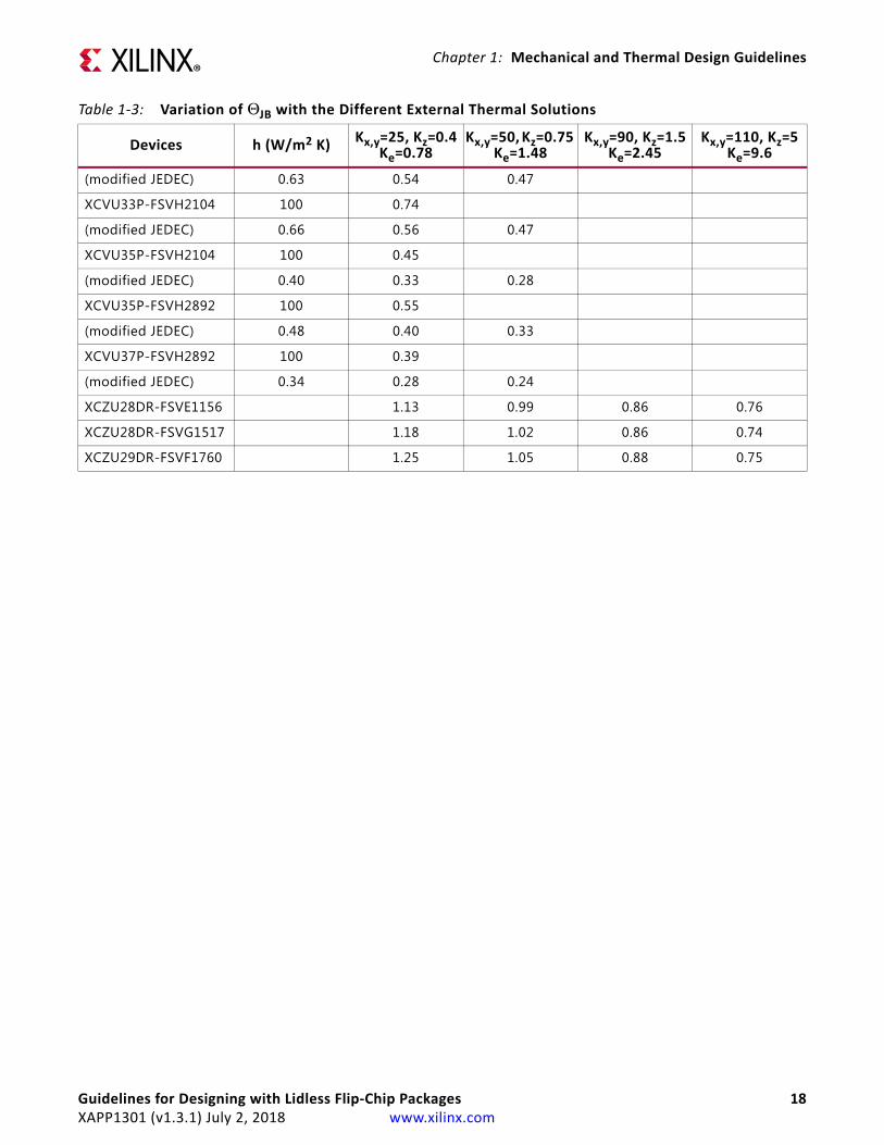
Table 1-2 shows the variation of ΘJC functions of the surrounding conditions and Table 1-3 shows the thermal resistance from junction to board, ΘJB, for the selected device/package combinations. The reported ΘJC and ΘJB enable comparison of different packages under the same condition.
Table 1-2: Variation of ΘJC with Different External Thermal Solution by Customer
Device h (W/m2 K) 100 1000 5000 10000 JEDEC
XCVU11P-D2104 ΘJC 0.004 0.004 0.004 0.004 0.004
XCVU9P-D2104 ΘJC 0.003 0.003 0.003 0.003 0.003
XCVU13P-D2104 ΘJC 0.003 0.003 0.003 0.003 0.003
XCVU31P-FSVH1924 ΘJC 0.367 0.324 0.247 0.213 0.055
XCVU33P-FSVH2104 ΘJC 0.306 0.270 0.208 0.180 0.034
XCVU35P-FSVH2104 ΘJC 0.145 0.127 0.100 0.088 0.017
XCVU35P-FSVH2892 ΘJC 0.142 0.126 0.099 0.087 0.017
XCVU37P-FSVH2892 ΘJC 0.086 0.078 0.065 0.059 0.013
XCZU28DR-FSVE1156 ΘJC 0.0189 0.0188 0.0186 0.0183 0.0164
XCZU28DR-FSVG1517 ΘJC 0.0190 0.0188 0.0185 0.0170 0.0164
XCZU29DR-FSVF1760 ΘJC 0.0190 0.0188 0.0185 0.0183 0.0164
Table 1-3: Variation of ΘJB with the Different External Thermal Solutions
Devices h (W/m2 K) Kx,y=25, Kz=0.4 Ke=0.78
Kx,y=50, Kz=0.75 Ke=1.48
Kx,y=90, Kz=1.5 Ke=2.45
Kx,y=110, Kz=5 Ke=9.6
XCVU11P-D2104 100 0.324 (modified JEDEC) 0.292 0.253 0.219
XCVU9P-D2104 100 0.340 (modified JEDEC) 0.300 0.257 0.220
XCVU13P-D2104 100 0.272 (modified JEDEC) 0.244 0.212 0.185
XCVU31P-FSVH1924 100 0.70
Guidelines for Designing with Lidless Flip-Chip Packages 17XAPP1301 (v1.3.1) July 2, 2018 www.xilinx.com
Chapter 1: Mechanical and Thermal Design Guidelines
(modified JEDEC) 0.63 0.54 0.47
XCVU33P-FSVH2104 100 0.74
(modified JEDEC) 0.66 0.56 0.47
XCVU35P-FSVH2104 100 0.45
(modified JEDEC) 0.40 0.33 0.28
XCVU35P-FSVH2892 100 0.55
(modified JEDEC) 0.48 0.40 0.33
XCVU37P-FSVH2892 100 0.39
(modified JEDEC) 0.34 0.28 0.24
XCZU28DR-FSVE1156 1.13 0.99 0.86 0.76
XCZU28DR-FSVG1517 1.18 1.02 0.86 0.74
XCZU29DR-FSVF1760 1.25 1.05 0.88 0.75
Table 1-3: Variation of ΘJB with the Different External Thermal Solutions
Devices h (W/m2 K) Kx,y=25, Kz=0.4 Ke=0.78
Kx,y=50, Kz=0.75 Ke=1.48
Kx,y=90, Kz=1.5 Ke=2.45
Kx,y=110, Kz=5 Ke=9.6
Guidelines for Designing with Lidless Flip-Chip Packages 18XAPP1301 (v1.3.1) July 2, 2018 www.xilinx.com

Chapter 1: Mechanical and Thermal Design Guidelines
The effective thermal conductivity of the PCB, ke, as referenced in Lemczyk et al. (1992)
Equation 1
The relation of ΘJB as a function of ke can be correlated as shown in Figure 1-10 through Figure 1-20:
For XCVU11P-D2104: ΘJB = 0.3063ke–0.157
X-Ref Target - Figure 1-10
Figure 1-10: XCVU11P-D2104: The Relationship between ΘJB and ke
ke
2 kxkz( )kx kz+----------------=
ke
RJB
(C/W
) X
X
X
0.360
X0.340
0.320
0.300
0.280
0.260
0.240
0.220
0.200
0.180
0.1600
(RJB based on modified JEDEC is 0.324)
RJB =0.3063ke-0.157
5 10 15 20 25 30
X20232-012318
Guidelines for Designing with Lidless Flip-Chip Packages 19XAPP1301 (v1.3.1) July 2, 2018 www.xilinx.com

Chapter 1: Mechanical and Thermal Design Guidelines
For XCVU9P-D2104: ΘJB = 0.318ke–0.173
For XCVU13P-D2104: ΘJB = 0.2564ke–0.154
X-Ref Target - Figure 1-11
Figure 1-11: XCVU9P-D2104: The Relationship between ΘJB and ke
X-Ref Target - Figure 1-12
Figure 1-12: XCVU13P-D2104: The Relationship between ΘJB and ke
ke
RJB
(C/W
)
X
X
X
0.360
X0.340
0.320
0.300
0.280
0.260
0.240
0.220
0.200
0.180
0.1600
(RJB based on modified JEDEC is 0.340)
RJB =0.318ke-0.173
5 10 15 20 25 30
X20233-012318
ke
RJB
(C/W
) X
XX
0.320
0.300
0.280
0.260
0.240
0.220
0.200
0.180
0.160
0
(RJB based on modified JEDEC is 0.272)
RJB =0.2564ke-0.154
5 10 15 20 25 300.140
X
X20231-012318
Guidelines for Designing with Lidless Flip-Chip Packages 20XAPP1301 (v1.3.1) July 2, 2018 www.xilinx.com

Chapter 1: Mechanical and Thermal Design Guidelines
For XCVU31P-FSVH1924: ΘJB = 0.66ke–0.16
For XCVU33P-FSVH2104 ΘJB = 0.6961ke–0.182
X-Ref Target - Figure 1-13
Figure 1-13: XCVU31P-FSVH1924: The Relationship between ΘJB and ke
X-Ref Target - Figure 1-14
Figure 1-14: XCVU33P-FSVH2104: The Relationship between ΘJB and ke
X20733-042418
X20732-042418
Guidelines for Designing with Lidless Flip-Chip Packages 21XAPP1301 (v1.3.1) July 2, 2018 www.xilinx.com

Chapter 1: Mechanical and Thermal Design Guidelines
For XCVU35P-FSVH2104 ΘJB = 0.4206ke–0.191
For XCVU35P-FSVH2892 ΘJB = 0.5115ke–0.205
X-Ref Target - Figure 1-15
Figure 1-15: XCVU35P-FSVH2104: The Relationship between ΘJB and ke
X-Ref Target - Figure 1-16
Figure 1-16: XCVU35P-FSVH2892: The Relationship between ΘJB and ke
X20731-042418
X20730-042418
Guidelines for Designing with Lidless Flip-Chip Packages 22XAPP1301 (v1.3.1) July 2, 2018 www.xilinx.com

Chapter 1: Mechanical and Thermal Design Guidelines
For XCVU37P-FSVH2892 ΘJB = 0.3606ke–0.194
For XCZU28DR-FSVE1156: ΘJB = 1.0518ke–0.156
X-Ref Target - Figure 1-17
Figure 1-17: XCVU37P-FSVH2892: The Relationship between ΘJB and ke
X-Ref Target - Figure 1-18
Figure 1-18: XCZU28DR-FSVE1156: The Relationship between ΘJB and ke
X20729-042418
X20727-042418
Guidelines for Designing with Lidless Flip-Chip Packages 23XAPP1301 (v1.3.1) July 2, 2018 www.xilinx.com

Chapter 1: Mechanical and Thermal Design Guidelines
For XCZU28DR-FSVG1517: ΘJB = 1.0895ke–0.185
For XCZU29DR-FSVF1760: ΘJB = 1.1382ke–0.2
X-Ref Target - Figure 1-19
Figure 1-19: XCZU28DR-FSVG1517: The Relationship between ΘJB and ke
X-Ref Target - Figure 1-20
Figure 1-20: XCZU29DR-FSVF1760: The Relationship between ΘJB and ke
X20728-042418
X20726-042418
Guidelines for Designing with Lidless Flip-Chip Packages 24XAPP1301 (v1.3.1) July 2, 2018 www.xilinx.com

Chapter 1: Mechanical and Thermal Design Guidelines
Detailed ModelA detailed thermal model is a direct representation of the device and package. This model provides geometric details describing the packaging, specifically in regards to the lid, TIM, die, under fill, substrate, and solder balls or leads. Each specific component in the detail model has associated material properties. When using the detailed model, account for the following:
1. Use the correct top surface contact for the package when modeling TIM on top of the detailed model, as the top surface contact may not be the actual full package size.
2. The Cu block included is a reference design of a Cu heat spreader contacting the heat sink with TIM2. The TIM of 70um thickness with a conductivity of 20 W/mK is represented in the model to provide effective correlation to the measurement results. This effective TIM1.5 reflects the contact surface etching of the Cu block in combination with the TIM material PCM780SP.
3. The temperature junction monitor point is at the die center. The junction monitor point needs to be positioned or added to the relevant location for your design.
4. The uniform power defined in the die is a default power and not necessarily realistic. You need to input the specific power requirement, especially if the power density varies throughout the die.
Due to the computationally intensive nature of this model, do not use it early in thermal management development when several iterations might be needed to find the solution. Instead, use the more agile simplified representation of the package, saving the detailed model for the end of the development cycle to more precisely verify the system's thermal margin.
For accurate results, a constructed model must accurately represent the package, especially if your simulation tool is not FloTHERM or IcePak. Since the reported simplified model is more accurate when compared to a detailed or two-resistor model, your simulations must account for any accuracy differences.
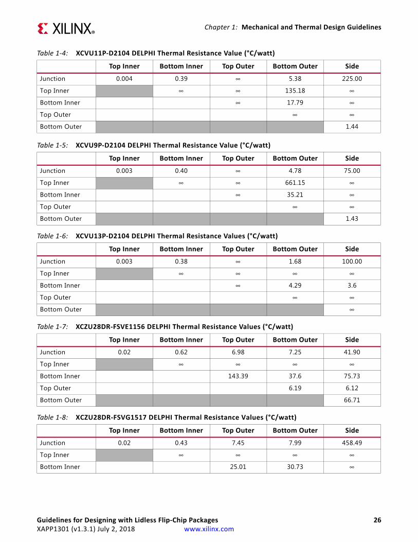
DELPHI ModelThe DELPHI model seeks to capture the thermal behavior of the packages more accurately at predetermined critical points (junction, case, top, leads, and so on) with the reduced set of nodes. Unlike a full 3D model, these are computationally efficient and work well in an integrated system simulation environment. The DELPHI model is more appropriate for estimating the value of the thermal solution in the early stages of a design.
The DELPHI model is available on the Xilinx support download center (under Model Type, see Package Thermal Models).
Table 1-4 through Table 1-6 show the thermal resistances for the devices using the D2104 packaging
Guidelines for Designing with Lidless Flip-Chip Packages 25XAPP1301 (v1.3.1) July 2, 2018 www.xilinx.com
Chapter 1: Mechanical and Thermal Design Guidelines
.
Table 1-4: XCVU11P-D2104 DELPHI Thermal Resistance Value (°C/watt)
Top Inner Bottom Inner Top Outer Bottom Outer Side
Junction 0.004 0.39 ∞ 5.38 225.00
Top Inner ∞ ∞ 135.18 ∞
Bottom Inner ∞ 17.79 ∞
Top Outer ∞ ∞
Bottom Outer 1.44
Table 1-5: XCVU9P-D2104 DELPHI Thermal Resistance Value (°C/watt)
Top Inner Bottom Inner Top Outer Bottom Outer Side
Junction 0.003 0.40 ∞ 4.78 75.00
Top Inner ∞ ∞ 661.15 ∞
Bottom Inner ∞ 35.21 ∞
Top Outer ∞ ∞
Bottom Outer 1.43
Table 1-6: XCVU13P-D2104 DELPHI Thermal Resistance Values (°C/watt)
Top Inner Bottom Inner Top Outer Bottom Outer Side
Junction 0.003 0.38 ∞ 1.68 100.00
Top Inner ∞ ∞ ∞ ∞
Bottom Inner ∞ 4.29 3.6
Top Outer ∞ ∞
Bottom Outer ∞
Table 1-7: XCZU28DR-FSVE1156 DELPHI Thermal Resistance Values (°C/watt)
Top Inner Bottom Inner Top Outer Bottom Outer Side
Junction 0.02 0.62 6.98 7.25 41.90
Top Inner ∞ ∞ ∞ ∞
Bottom Inner 143.39 37.6 75.73
Top Outer 6.19 6.12
Bottom Outer 66.71
Table 1-8: XCZU28DR-FSVG1517 DELPHI Thermal Resistance Values (°C/watt)
Top Inner Bottom Inner Top Outer Bottom Outer Side
Junction 0.02 0.43 7.45 7.99 458.49
Top Inner ∞ ∞ ∞ ∞
Bottom Inner 25.01 30.73 ∞
Guidelines for Designing with Lidless Flip-Chip Packages 26XAPP1301 (v1.3.1) July 2, 2018 www.xilinx.com

Chapter 1: Mechanical and Thermal Design Guidelines
DELPHI models are not provided for XCVU31P-FSVH1924, XCVU33P-FSVH2104, XCVU35P-FSVH2104, XCVU35P-FSVH2892, or XCVU37P-FSVH2892.
The DELPHI model is available precompiled in both Ansys IcePak and Mentor FloTHERM. If using a different thermal modeling tool, the DELPHI model can be constructed using the above thermal resistances. These thermal resistances must be in a block with the structure shown in Figure 1-21 and the dimensions specified in Table 1-10.
Top Outer 6.16 5.12
Bottom Outer 27.44
Table 1-9: XCZU28DR-FSVE1156 DELPHI Thermal Resistance Values (°C/watt)
Top Inner Bottom Inner Top Outer Bottom Outer Side
Junction 0.02 0.51 7.43 7.73 31.69
Top Inner ∞ ∞ ∞ ∞
Bottom Inner 59.99 63.63 230.15
Top Outer 6.16 4.60
Bottom Outer 18.79
Table 1-8: XCZU28DR-FSVG1517 DELPHI Thermal Resistance Values (°C/watt)
Top Inner Bottom Inner Top Outer Bottom Outer Side
Guidelines for Designing with Lidless Flip-Chip Packages 27XAPP1301 (v1.3.1) July 2, 2018 www.xilinx.com

Chapter 1: Mechanical and Thermal Design Guidelines
X-Ref Target - Figure 1-21
Figure 1-21: The Top Inner Area Location in the Top Outer Area
X18049-011718
Table 1-10: Top Inner and Top Outer Dimensions (mm)
DeviceTop Inner Top Outer Side
X Y X Y Z
XCVU11P-D2104 28.72 27.78 47.5 47.5 2.724
XCVU9P-D2104 25.55 34.44 47.5 47.5 2.724
XCVU13P-D2104 28.72 37.08 52.5 52.5 2.724
XCZU28DR-FSVE1156 21.13 18.144 35 35 2.272
XCZU28DR-FSVG1517 21.13 18.144 40 40 2.272
XCZU29DR-FSVF1760 21.13 18.144 42.5 42.5 2.272
Guidelines for Designing with Lidless Flip-Chip Packages 28XAPP1301 (v1.3.1) July 2, 2018 www.xilinx.com

Chapter 1: Mechanical and Thermal Design Guidelines
The bottom inner area is shown in Figure 1-22 and the dimensions are specified in Table 1-11.
For accurate results, ensure that the constructed model accurately represents the package, especially if the simulation tool is not FloTHERM or IcePak. The reported DELPHI model has better accuracy compared to the detail model versus solely the two-resistor model.
X-Ref Target - Figure 1-22
Figure 1-22: The Bottom Inner Area Location in the Bottom Outer Area
Table 1-11: Bottom Inner and Bottom Outer Dimensions (mm)
DeviceBottom Inner Bottom Outer
X Y X Y
XCVU11P-D2104 28.72 27.78 47.5 47.5
XCVU9P-D2104 25.56 34.46 47.5 47.5
XCVU13P-D2104 30.07 38.82 52.5 52.5
XCZU28DR-FSVE1156 21.22 18.22 35 35
XCZU28DR-FSVG1517 21.27 18.27 40 40
XCZU29DR-FSVF1760 21.27 18.27 42.5 42.5
X18050-102217
Guidelines for Designing with Lidless Flip-Chip Packages 29XAPP1301 (v1.3.1) July 2, 2018 www.xilinx.com

Chapter 1: Mechanical and Thermal Design Guidelines
Model ComparisonsThis section shows model comparisons between simplified models, DELPHI models, and detailed models, as available. Temperature comparisons are made using degrees Celsius. These comparisons are based on Icepak simulations.
Table 1-12: Comparison between the Detailed Model and Different DELPHI Model for XCVU11P-D2104
Boundary h (W/m2 K) Detailed Model DELPHI Model
Top Boundary100 X 0.999X
10000 X 1.000X
Bottom Boundary100 (ke = 0.78) X 0.991X
100 (ke = 9.6) X 1.009X
Table 1-13: Comparison between the Detailed Model and Different DELPHI Model for XCVU9P-D2104
Boundary h (W/m2 K) Detailed Model DELPHI Model
Top Boundary100 X 1.000X
10000 X 1.000X
Bottom Boundary100 (ke = 0.78) X 0.995X
100 (ke = 9.6) X 1.009X
Table 1-14: Comparison between the Detailed Model and Different DELPHI Model for XCVU13P-D2104
Boundary h (W/m2 K) Detailed Model DELPHI Model
Top Boundary100 X 1.000X
10000 X 0.929X
Bottom Boundary100 (ke = 0.78) X 1.040X
100 (ke = 9.6) X 1.054X
Table 1-15: Comparison between the Simplified Model and Detailed Model for XCVU31P-FSVH1924
Boundary h (W/m2 K) Detailed Model TJ Simplified Model TJ
Top Boundary100 X 1.0178X
10000 X 0.9860X
Bottom Boundary100 (ke = 0.78) X 1.0144X
100 (ke = 9.6) X 1.0310X
Guidelines for Designing with Lidless Flip-Chip Packages 30XAPP1301 (v1.3.1) July 2, 2018 www.xilinx.com

Chapter 1: Mechanical and Thermal Design Guidelines
Table 1-16: Comparison between the Simplified Model and Detailed Model for XCVU33P-FSVH2104
Boundary h (W/m2 K) Detailed Model TJ Simplified Model TJ
Top Boundary100 X 1.0126X
10000 X 0.9600X
Bottom Boundary100 (ke = 0.78) X 1.0106X
100 (ke = 9.6) X 1.0297X
Table 1-17: Comparison between the Simplified Model and Detailed Model for XCVU35P-FSVH2104
Boundary h (W/m2 K) Detailed Model TJ Simplified Model TJ
Top Boundary100 X 1.0114X
10000 X 0.9890X
Bottom Boundary100 (ke = 0.78) X 1.0083X
100 (ke = 9.6) X 1.0245X
Table 1-18: Comparison between the Simplified Model and Detailed Model for XCVU35P-FSVH2892
Boundary h (W/m2 K) Detailed Model TJ Simplified Model TJ
Top Boundary100 X 1.0103X
10000 X 0.9860X
Bottom Boundary100 (ke = 0.78) X 1.0126X
100 (ke = 9.6) X 1.0314X
Table 1-19: Comparison between the Simplified Model and Detailed Model for XCVU37P-FSVH2892
Boundary h (W/m2 K) Detailed Model TJ Simplified Model TJ
Top Boundary100 X 1.0100X
10000 X 0.9820X
Bottom Boundary100 (ke = 0.78) X 1.0086X
100 (ke = 9.6) X 1.0242X
Table 1-20: Comparison between the Detailed Model and DELPHI Model for XCZU28DR-FSVE1156
Boundary h (W/m2 K) Detailed Model TJ Detailed Model TJ
Top Boundary100 X 1.0002X
10000 X 0.9948X
Bottom Boundary100 (ke = 0.78) X 0.9938X
100 (ke = 9.6) X 0.9944X
Guidelines for Designing with Lidless Flip-Chip Packages 31XAPP1301 (v1.3.1) July 2, 2018 www.xilinx.com

Chapter 1: Mechanical and Thermal Design Guidelines
a
Example Heat Sink Thermal PerformanceFigure 1-23 through Figure 1-25 present graphical data extracted from experiments done using the detailed thermal model with the VU13P-FIGD2104.
Table 1-21: Comparison between the Detailed Model and DELPHI Model for XCZU28DR-FSVG1517
Boundary h (W/m2 K) Detailed Model TJ Detailed Model TJ
Top Boundary100 X 0.9998X
10000 X 0.9974X
Bottom Boundary100 (ke = 0.78) X 0.9867X
100 (ke = 9.6) X 0.9846X
Table 1-22: Comparison between the Detailed Model and DELPHI Model for XCZU29DR-FSVF1760
Boundary h (W/m2 K) Detailed Model TJ Detailed Model TJ
Top Boundary100 X 1.0003X
10000 X 0.9948X
Bottom Boundary100 (ke = 0.78) X 0.9762X
100 (ke = 9.6) X 0.9881X
X-Ref Target - Figure 1-23
Figure 1-23: Thermal Map Above Ambient at 30 CFM
Thermal Map above ambient @ambient @ 30CFM 150W Design
Core 118.75 W
25W 25W
25W 25W
25W
25W
Core 218.75 W
25W 25W
25W 25W
25W 25W
25W 25W
Core 318.75 W
25W 25W
25W 25W
25W 25W
25W 25W
Core 418.75 W
25W 25W
25W 25W
25W 25W
25W 25W
X20234-012318
Guidelines for Designing with Lidless Flip-Chip Packages 32XAPP1301 (v1.3.1) July 2, 2018 www.xilinx.com

Chapter 1: Mechanical and Thermal Design Guidelines
The graph data in Figure 1-24 and Figure 1-25 was extracted from thermal simulations using the VU13P-D2104 package models with the heat sink solution shown above for a 150 Watt FPGA design. Using the first graph on the left in Figure 1-24, with an air flow rate of 30 CFM, you can calculate an effective thermal resistance of ~0.23°C/Watt. Using the second graph (Figure 1-24, on the right), the thermal solution operating at that airflow measures (at SYSMON) approximately 35°C above ambient, implying that the maximum ambient under these conditions can be as high as 65°C. Using an equivalent lidded package like the B2104 would yield a maximum ambient temperature of 58°C (7°C lower), as shown in the experiment data in Figure 1-25.
X-Ref Target - Figure 1-24
Figure 1-24: 150W DesignX-Ref Target - Figure 1-25
Figure 1-25: Experimental Comparison between Lid and Lidless Devices
0.35
10
RH
S+T
IM2 (°
C/W
)
0.31
0.27
0.23
0.19
0.1520 30 40 50 60 70
50.0
0.16
Sys
Mon
Tem
pera
ture
(°C
)
45.0
40.0
35.0
30.0
25.00.32
RHS+TIM2 (°C/W) Flow Rate (CFM)
RHS+TIM2 = 0.808Flowrate-0.342
Lidless Package
Lidless Package
Lidless Package
Lidless Package
SysMon=153.69xRHS+TIM21.0777
X20235-022018
0.20 0.24 0.28
0.5
0.45
0.4
0.35
0.3
0.25
0.2
0.15
0.110 20 30 40 50 60 70
Lidless LID-PART Heat sink with heat pipesDimensions: 90x90x27mmBase thickness: 4.5mmFin Thickness is 0.16mmFin number is 72
92W 100W
RJ-A = 2.311CFM-0.645RJ-A = 2.3549CFM-0.599
CFM
Rj-a
X20236-012318
Guidelines for Designing with Lidless Flip-Chip Packages 33XAPP1301 (v1.3.1) July 2, 2018 www.xilinx.com

Chapter 1: Mechanical and Thermal Design Guidelines
The following pad recommendations are listed in the Recommended PCB Design Rules for BGA Packages chapter of UltraScale and UltraScale+ FPGAs Packaging and Pinouts Product Specification User Guide (UG575) [Ref 1].
• PCB Pad Recommendations
• Pad Type Recommendations
• Solder Pad Recommendation
Package Mechanical Loading SpecificationsFor this type of lidless FPGA package, the thermal management solution applies a mechanical load on the SSI die to ensure good thermal contact without any negative mechanical impact on the package. Therefore, the necessary applied pressure to ensure thermal performance of the thermal interface material between the heat sink base and the FPGA SSI die is in the range of 20 to 40 psi.
Removing Heat Sink Phase Change MaterialIf heat sinks are removed or reworked, the phase change material residue must be removed from the die surface. Laird Technologies, Inc. has provided the following guidance for complete removal of the phase change material from the component.
Instructions: 1. Separate the Components
2. Clean Remaining Residue with Solvent
3. First Aid
Separate the Components
At room temperature, use a back and forth twisting motion to break the bond between the phase change TIM and mated components (i.e., heat sink and CPU). See Figure 1-26.
Guidelines for Designing with Lidless Flip-Chip Packages 34XAPP1301 (v1.3.1) July 2, 2018 www.xilinx.com

Chapter 1: Mechanical and Thermal Design Guidelines
For smaller components (typically 15 mm x 15 mm or less), the bond usually breaks free easily at room temperature. For larger components, situations where minimal movement is available, or if using fragile components, heat the component (preferable) or heat sink to between 40°C and 60°C before removal.
While the guideline is between 40°C and 60°C, you might find that heating to 35°C is adequate. Others might prefer to heat to 70°C so that the phase change TIM is very soft and the components are easy to separate.
Clean Remaining Residue with Solvent
Using a clean cloth/wipe, wet it with one of the solvents below and wipe away any remaining residue.
• Toluene (best)
• Acetone (very good)
• Isoparaffinic hydrocarbon (trade names Isopar and Soltrol) (very good)
• Isopropyl alcohol (OK)
First Aid
Safe handling, disposal, and first aid measures for PCM780SP are included in the Laird Technologies MSDS. Read the MSDS before using or handling this product. It can be found on the Laird Technologies, Inc. website, www.lairdtech.com.
X-Ref Target - Figure 1-26
Figure 1-26: Breaking the Bond between TIM and Mated Components
Phase change
TIMHeat Sink
CPU
Guidelines for Designing with Lidless Flip-Chip Packages 35XAPP1301 (v1.3.1) July 2, 2018 www.xilinx.com

Chapter 1: Mechanical and Thermal Design Guidelines
Measurement DebugWhen performing in-system thermal testing, to ensure accurate data and not incur damage to the device, do not place a thermocouple in between the die and the heat sink. On the extreme side, it might cause additional mechanical and/or thermal stress to the die, leading to damage. Even if damage does not occur, it often leads to thicker and or uneven TIM thickness, leading to different thermal performance from a system without the thermocouple. To obtain the device temperature, use System Monitor (SYSMON) because it is an non-invasive means to get accurate die measurements while debugging the system.
Reference Design FilesDownload the reference design files for this application note from the Xilinx website.
ConclusionThis application note addresses the specific mechanical and thermal design requirements of the device and package combinations listed in Table 1-1. Further information on removing a heat sink, including removal of phase change material, is available in the UltraScale and UltraScale+ FPGAs Packaging and Pinouts Product Specification User Guide (UG575) [Ref 1].
Guidelines for Designing with Lidless Flip-Chip Packages 36XAPP1301 (v1.3.1) July 2, 2018 www.xilinx.com

Appendix A
Recommended Thermal Solution Installation of Xilinx FCBGA Lidless Packages
OverviewThis appendix presents the recommended installation procedure for the Xilinx FCBGA lidless packages. These devices are capable of generating high power and thus large amounts of heat, so a thermal solution (cooler) is required to dissipate the energy to keep the device working within the specific operating temperature limits. Attaching the cooler to the device with fasteners can be a challenge while not damaging the silicon.
ChallengesTo achieve the best thermal conductivity, the interface between the silicon and cooler must have very good contact. Due to inevitable mechanical limitations, the two surfaces are not perfectly flat or smooth and a Thermal Interface Material (TIM) is typically applied to fill any imperfections.
The TIM grain size must be smaller than the gaps so it is only filling the voids and not creating a thick bond line between the two devices. A certain pressure is required to hold the two devices together, maintaining minimum bond line and not damaging the silicon. This pressure is usually provided by the device manufacturer.
The device should be attached to the thermal solution by mechanical fasteners. The installation process has to be well designed so that the pressure is evenly distributed over the silicon surface and the two surfaces are parallel with a specific pressure. The TIM is evenly spread filling the voids and maintaining the minimum bond line.
Guidelines for Designing with Lidless Flip-Chip Packages 37XAPP1301 (v1.3.1) July 2, 2018 www.xilinx.com

Appendix A: Recommended Thermal Solution Installation of Xilinx FCBGA Lidless
Installation ControlThe assembly floor should have similar tools as listed here to ensure that the thermal solution is appropriately assembled on the top of the FCBGA.
Equipment and CalibrationThe equipment used for the mechanical installation process are:
• Adjustable torque screwdriver (Figure A-1) and calibrator (Figure A-2)
• Tekscan FlexiForce A502 pressure gauge with multiple handle ELF system (Figure A-3)
• Tactilus free form square pressure sensors (Figure A-4)X-Ref Target - Figure A-1
Figure A-1: Digital Torque Screwdriver (Top) and Hios CL 2000 (Bottom)
Guidelines for Designing with Lidless Flip-Chip Packages 38XAPP1301 (v1.3.1) July 2, 2018 www.xilinx.com

Appendix A: Recommended Thermal Solution Installation of Xilinx FCBGA Lidless
X-Ref Target - Figure A-2
Figure A-2: Screw Torque Calibrator – Hios HP-10
X-Ref Target - Figure A-3
Figure A-3: Pressure Gauge – Tekscan FlexiForce A502 Multiple Handle ELF System
Guidelines for Designing with Lidless Flip-Chip Packages 39XAPP1301 (v1.3.1) July 2, 2018 www.xilinx.com

Appendix A: Recommended Thermal Solution Installation of Xilinx FCBGA Lidless
X-Ref Target - Figure A-4
Figure A-4: Pressure Sensor – Tactilus Free Form Square Sensors
Tactilus Free Form Square Sensor 8 mmDimension: 8 mm x 8 mmApproximate Pressure Range: 0-200 psiThickness: 0.22 mm
Tactilus Free Form Square Sensor 22 mmDimension: 22 mm x 22 mmApproximate Pressure Range: 0-200 psiThickness: 0.25 mm
Tactilus Free Form Square Sensor 40 mmDimension: 40 mm x 40 mmApproximate Pressure Range: 0-50 psiThickness: 0.25 mm
X20661-041318
X-Ref Target - Figure A-5
Figure A-5: Tekscan Pressure Sensor – Zoomed In
Guidelines for Designing with Lidless Flip-Chip Packages 40XAPP1301 (v1.3.1) July 2, 2018 www.xilinx.com

Appendix A: Recommended Thermal Solution Installation of Xilinx FCBGA Lidless
Set Up and CalibrationThe torque of the screwdriver is calibrated by the calibrator and set to the torque (calculated based on the required pressure, die surface area) using the digital torque meter. For guidelines on pressure recommendations, see Heat Sink Pressure.
Note: Calibration of the digital torque calibrator/meter is done annually.
Process Qualification
Pressure and Force Verification
The spring screw or clip has to be designed with the required force that can achieve the target pressure at the interface between the die surface and the cooler. For example,
Target pressure = 32 psi
Die size = 0.5 inch by 0.5 inch
Target force = 32 psi × 0.5 inch × 0.5 inch = 8 lb
Installation Verification
Use the exact FCBGA, PCB, and thermal solution with the screws verified in the previous section. Install and verify if the target is achieved.
Guidelines for Designing with Lidless Flip-Chip Packages 41XAPP1301 (v1.3.1) July 2, 2018 www.xilinx.com

Appendix A: Recommended Thermal Solution Installation of Xilinx FCBGA Lidless
Figure A-6 shows the FCBGA board layouts.
The target force can be reproduced and the force exerted on the die surface is close to the target of 32 psi.
Installation ProcessThere are different approaches to assemble the heat thermal solution on the FCBGA. This depends on the type of mechanical attachment. The following examples illustrate how the screws affect the thermal solution from either the back side of the board or the front side of the board.
X-Ref Target - Figure A-6
Figure A-6: FCBGA Board Layouts
X-Ref Target - Figure A-7
Figure A-7: Target Force
Guidelines for Designing with Lidless Flip-Chip Packages 42XAPP1301 (v1.3.1) July 2, 2018 www.xilinx.com

Appendix A: Recommended Thermal Solution Installation of Xilinx FCBGA Lidless
Heat Sink Assembly for Dynamic Back Side Mounting
This example is given based on the PCIe card, which has the following items:
• Board back plate (Figure A-8)
• PCIe component (Figure A-9)
• Active heat sink (Figure A-10)X-Ref Target - Figure A-8
Figure A-8: Board Back Plate
Guidelines for Designing with Lidless Flip-Chip Packages 43XAPP1301 (v1.3.1) July 2, 2018 www.xilinx.com

Appendix A: Recommended Thermal Solution Installation of Xilinx FCBGA Lidless
Figure A-11 shows a flowchart of the heat sink assembly.
X-Ref Target - Figure A-9
Figure A-9: PCIe Card
X-Ref Target - Figure A-10
Figure A-10: Active Heat Sink Assembly
Guidelines for Designing with Lidless Flip-Chip Packages 44XAPP1301 (v1.3.1) July 2, 2018 www.xilinx.com

Appendix A: Recommended Thermal Solution Installation of Xilinx FCBGA Lidless
X-Ref Target - Figure A-11
Figure A-11: Flowchart of the Heat Sink Assembly
Heat sink assembly of PCIe card.
Assembly completed.
Acquire components: back plate, PCIe card, and heat sink.
Attach back plate to PCIe card using the jig.
Position PCIe card in the jig and align with the heat sink screw holes.
Place heat sink into the jig template.
Fasten and tighten screws with the appropriate torque to attach heat sink.
X20654-041318
Guidelines for Designing with Lidless Flip-Chip Packages 45XAPP1301 (v1.3.1) July 2, 2018 www.xilinx.com

Appendix A: Recommended Thermal Solution Installation of Xilinx FCBGA Lidless
The following details the assembly procedure for the heat sink. Before you begin, Figure A-12 shows a jig template which is critical for smooth and faster alignment during assembly.
X-Ref Target - Figure A-12
Figure A-12: Jig Template
Guidelines for Designing with Lidless Flip-Chip Packages 46XAPP1301 (v1.3.1) July 2, 2018 www.xilinx.com

Appendix A: Recommended Thermal Solution Installation of Xilinx FCBGA Lidless
1. Place the active heat sink into position of the jig with contact surface facing up.
2. Position the PCIe card and back plate on the top of the heat sink. This placement is aligned using the jig.
X-Ref Target - Figure A-13
Figure A-13: Active Heat Sink in Jig
X-Ref Target - Figure A-14
Figure A-14: PCIe Card with Back Plate in Jig
Guidelines for Designing with Lidless Flip-Chip Packages 47XAPP1301 (v1.3.1) July 2, 2018 www.xilinx.com

Appendix A: Recommended Thermal Solution Installation of Xilinx FCBGA Lidless
3. Lightly fasten the four screws numbered. Use the preset torque screwdriver to tighten screws in the number sequence to finish assembly.
X-Ref Target - Figure A-15
Figure A-15: Screw Sequence for Final Assembly
Guidelines for Designing with Lidless Flip-Chip Packages 48XAPP1301 (v1.3.1) July 2, 2018 www.xilinx.com

Appendix A: Recommended Thermal Solution Installation of Xilinx FCBGA Lidless
4. The assembly is complete.
Heat Sink Assembly for Dynamic Top Side Mounting of Lidless Unit
The following components are used for this heat sink assembly:
• Heat sink and back clip (Figure A-17)
• PCB board (Figure A-18)
X-Ref Target - Figure A-16
Figure A-16: Assembly Completed
Guidelines for Designing with Lidless Flip-Chip Packages 49XAPP1301 (v1.3.1) July 2, 2018 www.xilinx.com

Appendix A: Recommended Thermal Solution Installation of Xilinx FCBGA Lidless
X-Ref Target - Figure A-17
Figure A-17: Heat Sink and Back Clip
X-Ref Target - Figure A-18
Figure A-18: PCB Board
Guidelines for Designing with Lidless Flip-Chip Packages 50XAPP1301 (v1.3.1) July 2, 2018 www.xilinx.com

Appendix A: Recommended Thermal Solution Installation of Xilinx FCBGA Lidless
Figure A-19 shows a flowchart of the heat sink assembly for a lidless unit.
X-Ref Target - Figure A-19
Figure A-19: Flowchart of the Heat Sink Assembly
Heat sink assembly of lidless unit.
Assembly completed.
Acquire components: PCB board and heat sink.
Position PCB board in the jig and align with the back clip screw holes.
Place heat sink back clip into the jig template.
Fasten and tighten screws with the appropriate torque to attach heat sink.
Place heat sink on top of lidless unit and align with back clip screw holes.
X20655-041318
Guidelines for Designing with Lidless Flip-Chip Packages 51XAPP1301 (v1.3.1) July 2, 2018 www.xilinx.com

Appendix A: Recommended Thermal Solution Installation of Xilinx FCBGA Lidless
The following details the assembly procedure for the heat sink. Before you begin, Figure A-20 shows a jig template which can be used during assembly.
1. Place the heat sink back clip into the defined position of the jig template.
X-Ref Target - Figure A-20
Figure A-20: Jig Template
X-Ref Target - Figure A-21
Figure A-21: Heat Sink in Jig
Guidelines for Designing with Lidless Flip-Chip Packages 52XAPP1301 (v1.3.1) July 2, 2018 www.xilinx.com

Appendix A: Recommended Thermal Solution Installation of Xilinx FCBGA Lidless
2. Position the test board with the lidless unit on top of the heat sink back clip into the defined position of the jig template.
3. Place the heat sink on top of the lidless unit on the board. Align to the screw holes (highlighted in red) of the back clip.
X-Ref Target - Figure A-22
Figure A-22: Test Board and Lidless Unit in Jig
X-Ref Target - Figure A-23
Figure A-23: Screw Locations for Heat Sink and Lidless Unit in Jig
Guidelines for Designing with Lidless Flip-Chip Packages 53XAPP1301 (v1.3.1) July 2, 2018 www.xilinx.com

Appendix A: Recommended Thermal Solution Installation of Xilinx FCBGA Lidless
4. Lightly fasten the screws to hold the clip. Use the preset screwdriver to tighten the four screws of the heat sink in the following sequence to finish assembly.
X-Ref Target - Figure A-24
Figure A-24: Heat Sink and Lidless Unit in Jig
X-Ref Target - Figure A-25
Figure A-25: Screw Sequence for Final Assembly
Guidelines for Designing with Lidless Flip-Chip Packages 54XAPP1301 (v1.3.1) July 2, 2018 www.xilinx.com

Appendix A: Recommended Thermal Solution Installation of Xilinx FCBGA Lidless
Heat Sink Assembly for Dynamic Bottom Side Mounting of Wireless Heat Sink
The following components are used for this heat sink assembly:
• Lidless unit on board (Figure A-26)
• Cu block with pedestal (Figure A-27)
• Heat sink for wireless application (Figure A-28) X-Ref Target - Figure A-26
Figure A-26: Lidless Unit on Board
X-Ref Target - Figure A-27
Figure A-27: Cu Block with Pedestal – Bottom Side and Top Side
Guidelines for Designing with Lidless Flip-Chip Packages 55XAPP1301 (v1.3.1) July 2, 2018 www.xilinx.com

Appendix A: Recommended Thermal Solution Installation of Xilinx FCBGA Lidless
Figure A-29 shows a flowchart of the heat sink assembly for a wireless application.
X-Ref Target - Figure A-28
Figure A-28: Heat Sink for Wireless Application
X-Ref Target - Figure A-29
Figure A-29: Flowchart of the Heat Sink Assembly
Heat sink assembly for wireless.
Assembly completed.
Acquire components: Cu block, PCB board, and heat sink.
Fasten and tighten screws with appropriate torque to attach Cu block.
Position PCB board into the jig and align with Cu block screw holes.
Fasten and tighten screws with the appropriate torque to attach heat sink.
Place assembled board with Cu block into jig on top of heat sink and align.
Place Cu block into the jig template.
X20657-041318
Guidelines for Designing with Lidless Flip-Chip Packages 56XAPP1301 (v1.3.1) July 2, 2018 www.xilinx.com

Appendix A: Recommended Thermal Solution Installation of Xilinx FCBGA Lidless
The following details the assembly procedure for the heat sink. Before you begin, Figure A-30 and Figure A-31 show the jig templates that can be used during assembly.
X-Ref Target - Figure A-30
Figure A-30: Jig Template for Cu Block with PedestalX-Ref Target - Figure A-31
Figure A-31: Jig Template for Wireless Heat Sink and Board
Guidelines for Designing with Lidless Flip-Chip Packages 57XAPP1301 (v1.3.1) July 2, 2018 www.xilinx.com

Appendix A: Recommended Thermal Solution Installation of Xilinx FCBGA Lidless
1. Apply thermal interface material to the Cu block pedestal.
2. Place Cu block into the defined location of the jig template.
3. Flip over and position board on top of the Cu block in the jig and align to screw holes (highlighted in red) of Cu block.
X-Ref Target - Figure A-32
Figure A-32: Thermal Interface Material to Cu Block Pedestal
X-Ref Target - Figure A-33
Figure A-33: Cu Block in Jig
X-Ref Target - Figure A-34
Figure A-34: Screw Locations for Cu Block on Board
Guidelines for Designing with Lidless Flip-Chip Packages 58XAPP1301 (v1.3.1) July 2, 2018 www.xilinx.com

Appendix A: Recommended Thermal Solution Installation of Xilinx FCBGA Lidless
4. Rotate the screws for a couple turns to hold the board in place. Use the preset screwdriver to tighten the four screws of the heat sink in the sequence as shown.
5. Finish assembled board with the Cu block.
X-Ref Target - Figure A-35
Figure A-35: Screw Sequence for Board
X-Ref Target - Figure A-36
Figure A-36: Assembled Board with Cu Block
Guidelines for Designing with Lidless Flip-Chip Packages 59XAPP1301 (v1.3.1) July 2, 2018 www.xilinx.com

Appendix A: Recommended Thermal Solution Installation of Xilinx FCBGA Lidless
6. Place heat sink into the defined location of the jig.
7. Assemble board with the Cu block on top of the heat sink. Align to screw holes (highlighted in red) of the heat sink.
X-Ref Target - Figure A-37
Figure A-37: Heat Sink in Jig
X-Ref Target - Figure A-38
Figure A-38: Screw Locations for Cu Block on Heat Sink
Guidelines for Designing with Lidless Flip-Chip Packages 60XAPP1301 (v1.3.1) July 2, 2018 www.xilinx.com

Appendix A: Recommended Thermal Solution Installation of Xilinx FCBGA Lidless
8. Fasten screws in the appropriate sequence to finish assembly X-Ref Target - Figure A-39
Figure A-39: Screw Sequence for Final Assembly
Guidelines for Designing with Lidless Flip-Chip Packages 61XAPP1301 (v1.3.1) July 2, 2018 www.xilinx.com

Appendix B
Additional Resources and Legal Notices
Xilinx ResourcesFor support resources such as Answers, Documentation, Downloads, and Forums, see Xilinx Support.
Solution CentersSee the Xilinx Solution Centers for support on devices, software tools, and intellectual property at all stages of the design cycle. Topics include design assistance, advisories, and troubleshooting tips.
Documentation Navigator and Design HubsXilinx® Documentation Navigator provides access to Xilinx documents, videos, and support resources, which you can filter and search to find information. To open the Xilinx Documentation Navigator (DocNav):
• From the Vivado® IDE, select Help > Documentation and Tutorials.
• On Windows, select Start > All Programs > Xilinx Design Tools > DocNav.
• At the Linux command prompt, enter docnav.
Xilinx Design Hubs provide links to documentation organized by design tasks and other topics, which you can use to learn key concepts and address frequently asked questions. To access the Design Hubs:
• In the Xilinx Documentation Navigator, click the Design Hubs View tab.
• On the Xilinx website, see the Design Hubs page.
Note: For more information on Documentation Navigator, see the Documentation Navigator page on the Xilinx website.
Guidelines for Designing with Lidless Flip-Chip Packages 62XAPP1301 (v1.3.1) July 2, 2018 www.xilinx.com

Appendix B: Additional Resources and Legal Notices
ReferencesFor additional information on heat management and contact information:
1. UltraScale and UltraScale+ FPGAs Packaging and Pinouts Product Specification User Guide (UG575)
2. Zynq UltraScale+ MPSoC Technical Reference Manual (UG1085)
3. Virtex UltraScale+ FPGA Package Thermal Models (Xilinx support)
Refer to the following websites for CFD tools supported by Xilinx with thermal models:
1. Mentor (FloTHERM)
2. ANSYS (IcePak)
Refer to the following papers on thermal modeling:
1. Lemczyk, T.F., Mack, B., Culham, J.R. and Yovanovich, M.M., 1992, “Printed Circuit Board Trace Thermal Analysis and Effective Conductivity,” ASME J. Electronic Packaging, Vol. 114, pp. 413 - 419.
2. Refai-Ahmed, G. and Karimanal, K., 2003, “Validation of Compact Conduction Models of BGA Under Realistic Boundary,” J. of Components and Packaging Technology, Vol. 26, No. 3, pp. 610-615.
3. Sansoucy, E, Refai-Ahmed, G., and Karimanal, K., 2002, “Thermal Characterization of TBGA Package for an integration in Board Level Analysis,” Eighth Intersociety on Thermal Conference Phenomena in Electronic Systems, San Diego., USA.
4. Karimanal, K. and Refai-Ahmed, G., 2002, “Validation of Compact Conduction Models of BGA Under Realistic Boundary Conditions,” Eighth Intersociety on Thermal Conference Phenomena in Electronic Systems, San Diego, USA.
5. Karimanal, K. and Refai-Ahmed, G., 2001, “Compact conduction Model (CCM) of Microelectronic Packages—a BGA Validation Study,” APACK Conference on Advance in Packaging, Singapore.
Guidelines for Designing with Lidless Flip-Chip Packages 63XAPP1301 (v1.3.1) July 2, 2018 www.xilinx.com

Appendix B: Additional Resources and Legal Notices
Please Read: Important Legal NoticesThe information disclosed to you hereunder (the “Materials”) is provided solely for the selection and use of Xilinx products. To the maximum extent permitted by applicable law: (1) Materials are made available "AS IS" and with all faults, Xilinx hereby DISCLAIMS ALL WARRANTIES AND CONDITIONS, EXPRESS, IMPLIED, OR STATUTORY, INCLUDING BUT NOT LIMITED TO WARRANTIES OF MERCHANTABILITY, NON-INFRINGEMENT, OR FITNESS FOR ANY PARTICULAR PURPOSE; and (2) Xilinx shall not be liable (whether in contract or tort, including negligence, or under any other theory of liability) for any loss or damage of any kind or nature related to, arising under, or in connection with, the Materials (including your use of the Materials), including for any direct, indirect, special, incidental, or consequential loss or damage (including loss of data, profits, goodwill, or any type of loss or damage suffered as a result of any action brought by a third party) even if such damage or loss was reasonably foreseeable or Xilinx had been advised of the possibility of the same. Xilinx assumes no obligation to correct any errors contained in the Materials or to notify you of updates to the Materials or to product specifications. You may not reproduce, modify, distribute, or publicly display the Materials without prior written consent. Certain products are subject to the terms and conditions of Xilinx’s limited warranty, please refer to Xilinx’s Terms of Sale which can be viewed at https://www.xilinx.com/legal.htm#tos; IP cores may be subject to warranty and support terms contained in a license issued to you by Xilinx. Xilinx products are not designed or intended to be fail-safe or for use in any application requiring fail-safe performance; you assume sole risk and liability for use of Xilinx products in such critical applications, please refer to Xilinx’s Terms of Sale which can be viewed at https://www.xilinx.com/legal.htm#tos.AUTOMOTIVE APPLICATIONS DISCLAIMERAUTOMOTIVE PRODUCTS (IDENTIFIED AS “XA” IN THE PART NUMBER) ARE NOT WARRANTED FOR USE IN THE DEPLOYMENT OF AIRBAGS OR FOR USE IN APPLICATIONS THAT AFFECT CONTROL OF A VEHICLE (“SAFETY APPLICATION”) UNLESS THERE IS A SAFETY CONCEPT OR REDUNDANCY FEATURE CONSISTENT WITH THE ISO 26262 AUTOMOTIVE SAFETY STANDARD (“SAFETY DESIGN”). CUSTOMER SHALL, PRIOR TO USING OR DISTRIBUTING ANY SYSTEMS THAT INCORPORATE PRODUCTS, THOROUGHLY TEST SUCH SYSTEMS FOR SAFETY PURPOSES. USE OF PRODUCTS IN A SAFETY APPLICATION WITHOUT A SAFETY DESIGN IS FULLY AT THE RISK OF CUSTOMER, SUBJECT ONLY TO APPLICABLE LAWS AND REGULATIONS GOVERNING LIMITATIONS ON PRODUCT LIABILITY.© Copyright 2017–2018 Xilinx, Inc. Xilinx, the Xilinx logo, Artix, ISE, Kintex, Spartan, Virtex, Vivado, Zynq, and other designated brands included herein are trademarks of Xilinx in the United States and other countries. All other trademarks are the property of their respective owners.
Guidelines for Designing with Lidless Flip-Chip Packages 64XAPP1301 (v1.3.1) July 2, 2018 www.xilinx.com