
MEC1322 Data Sheet - Microchip Technologyww1.microchip.com/downloads/en/DeviceDoc/00001719D.pdf ·...
456
2014 - 2015 Microchip Technology Inc. DS00001719D-page 1 Product Features • ARM ® Cortex ® -M4 Processor Core - 32-Bit ARM v7-M Instruction Set Architecture - Hardware Floating Point Unit (FPU) - Single 4GByte Addressing Space (Von Neu- mann Model) - Little-Endian Byte Ordering - Bit-Banding Feature Included - NVIC Nested Vectored Interrupt Controller - Up to 240 Individually-Vectored Interrupt Sources Supported - 8 Levels of Priority, Individually Assignable By Vector - Chip-Level Interrupt Aggregator supported, to expand number of interrupt sources or reduce number of vectors - System Tick Timer - Complete ARM-Standard Debug Support - JTAG-Based DAP Port, Comprised of SWJ-DP and AHB-AP Debugger Access Functions - Full DWT Hardware Functionality: 4 Data Watchpoints and Execution Monitoring - Full FPB Hardware Breakpoint Functionality: 6 Execution Breakpoints and 2 Literal (Data) Breakpoints - Comprehensive ARM-Standard Trace Sup- port - Full DWT Hardware Trace Functionality for Watchpoint and Performance Monitoring - Full ITM Hardware Trace Functionality for Instrumented Firmware Support and Profiling - Full ETM Hardware Trace Functionality for Instruction Trace - Full TPIU Functionality for Trace Output Communication • 128K SRAM (Code or Data) - 96K Optimized for Code - 32K Optimized for Data • LPC Interface - Supports LPC Bus frequencies of 19MHz to 33MHz - LPC I/O Cycles Decoded - LPC Memory Cycles Decoded - Clock Run Support - Serial IRQ - ACPI SCI interface - SMI# output • Two SPI Memory Interfaces - 3-pin Full Duplex serial communication interface - Two Private and Two Shared Chip Selects - DMA Support • 8042 Style Host Interface - Mailbox Registers Interface - Forty-three 8-Bit scratch registers - Two Register Mailbox Command Interface - Two Register SMI Source Interface • Two ACPI Embedded Controller Interface - 1 or 4 Byte Data transfer capable • ACPI Power Management Interface - SCI Event-Generating Functions • Embedded Memory Interface - Host Serial IRQ Source - Provides Two Windows to On-Chip SRAM for Host Access • Two Register Mailbox Command Interface • Battery Backed (VCC0/VBAT) Resources - Power Fail Register - Power-Fail Status Register - Battery backed 64 byte memory • Real Time Clock (RTC) - VCC0 (VBAT) Powered - 32KHz Crystal Oscillator - 32KHz Clock output available under VCC1 power - Time-of-Day and Calendar Registers - Programmable Alarms - Supports Leap Year and Daylight Savings Time • Hibernation Timers • General Purpose Analog to Digital Converter - 10-bit conversion precision - 10-bit conversion per channel is completed in less than 12us - 5 ADC channels - 10-bit Conversion with 2.9mV resolution - 0 to 3.3 VDC Conversion Range - Optional continuous sampling at a programmable rate - Internal Analog Voltage Reference (3.0V +/- 1%) • Watch Dog Timer • Four Programmable 16-bit and Two 32-bit Timers - Wake-capable Auto-reloading Timers • Four Independent Hardware Driven PS/2 Ports - Fully functional on Main and/or Suspend Power - PS/2 Edge Wake Capable • Four Programmable Pulse-Width Modulator Out- puts - Independent Clock Rates - 16-Bit Duty Cycle Granularity - Operational in both Full on and Standby modes MEC1322 Keyboard and Embedded Controller for Notebook PC
Transcript of MEC1322 Data Sheet - Microchip Technologyww1.microchip.com/downloads/en/DeviceDoc/00001719D.pdf ·...

MEC1322Keyboard and Embedded Controller for Notebook PC
Product Features
• ARM® Cortex®-M4 Processor Core- 32-Bit ARM v7-M Instruction Set Architecture- Hardware Floating Point Unit (FPU) - Single 4GByte Addressing Space (Von Neu-
mann Model) - Little-Endian Byte Ordering - Bit-Banding Feature Included - NVIC Nested Vectored Interrupt Controller
- Up to 240 Individually-Vectored Interrupt Sources Supported
- 8 Levels of Priority, Individually Assignable By Vector - Chip-Level Interrupt Aggregator supported, to
expand number of interrupt sources or reduce number of vectors
- System Tick Timer - Complete ARM-Standard Debug Support
- JTAG-Based DAP Port, Comprised of SWJ-DP and AHB-AP Debugger Access Functions
- Full DWT Hardware Functionality: 4 Data Watchpoints and Execution Monitoring
- Full FPB Hardware Breakpoint Functionality: 6 Execution Breakpoints and 2 Literal (Data) Breakpoints
- Comprehensive ARM-Standard Trace Sup-port - Full DWT Hardware Trace Functionality for
Watchpoint and Performance Monitoring - Full ITM Hardware Trace Functionality for
Instrumented Firmware Support and Profiling- Full ETM Hardware Trace Functionality for
Instruction Trace - Full TPIU Functionality for Trace Output
Communication • 128K SRAM (Code or Data)
- 96K Optimized for Code- 32K Optimized for Data
• LPC Interface- Supports LPC Bus frequencies of 19MHz to
33MHz- LPC I/O Cycles Decoded- LPC Memory Cycles Decoded- Clock Run Support- Serial IRQ- ACPI SCI interface- SMI# output
• Two SPI Memory Interfaces- 3-pin Full Duplex serial communication interface- Two Private and Two Shared Chip Selects- DMA Support
• 8042 Style Host Interface- Mailbox Registers Interface
- Forty-three 8-Bit scratch registers- Two Register Mailbox Command Interface- Two Register SMI Source Interface
• Two ACPI Embedded Controller Interface- 1 or 4 Byte Data transfer capable
• ACPI Power Management Interface- SCI Event-Generating Functions
• Embedded Memory Interface- Host Serial IRQ Source- Provides Two Windows to On-Chip SRAM for
Host Access• Two Register Mailbox Command Interface• Battery Backed (VCC0/VBAT) Resources
- Power Fail Register- Power-Fail Status Register- Battery backed 64 byte memory
• Real Time Clock (RTC)- VCC0 (VBAT) Powered- 32KHz Crystal Oscillator- 32KHz Clock output available under VCC1
power- Time-of-Day and Calendar Registers- Programmable Alarms- Supports Leap Year and Daylight Savings
Time• Hibernation Timers• General Purpose Analog to Digital Converter
- 10-bit conversion precision- 10-bit conversion per channel is completed in
less than 12us- 5 ADC channels
- 10-bit Conversion with 2.9mV resolution- 0 to 3.3 VDC Conversion Range
- Optional continuous sampling at a programmable rate
- Internal Analog Voltage Reference (3.0V +/-1%)
• Watch Dog Timer• Four Programmable 16-bit and Two 32-bit Timers
- Wake-capable Auto-reloading Timers • Four Independent Hardware Driven PS/2 Ports
- Fully functional on Main and/or Suspend Power
- PS/2 Edge Wake Capable• Four Programmable Pulse-Width Modulator Out-
puts - Independent Clock Rates- 16-Bit Duty Cycle Granularity- Operational in both Full on and Standby modes
2014 - 2015 Microchip Technology Inc. DS00001719D-page 1

MEC1322
• Four EC-based SMBus 2.0 Host Controllers- Allows Master or Dual Slave Operation- Controllers are Fully Operational on Standby
Power- DMA-driven I2C Network Layer Hardware- I2C Datalink Compatibility Mode- Multi-Master Capable- Supports Clock Stretching- Programmable Bus Speeds
- 400 KHz Fast-mode Capable- 1 Mbps Fast-mode Plus Capable
- Hardware Bus Access "Fairness" Interface- SMBus Time-outs Interface- 5 Ports- 2 Port Flexible Multiplexing
• PECI 3.0 Interface• Keyboard Matrix Scan Interface
- 18 x 8 Interrupt/Wake Capable Multiplexed Keyboard Scan Matrix
- Row Predrive Option• Four Breathing/Blinking LED Interfaces
- Programmable Blink Rates- Piecewise Linear Breathing LED Output Con-
troller- Operational in EC Sleep States
• Dual Fan Tachometer Inputs• RPM-Based Fan Speed Control Algorithm
- Utilizes one TACH input and one PWM output- 3% accurate from 500 RPM to 16k RPM- Automatic Tachometer feedback- Aging Fan or Invalid Drive Detection- Spin Up Routine- Ramp Rate Control- RPM-based Fan Speed Control Algorithm
• Fast GATEA20 & Fast CPU_RESET• RSMRST# Functionality Supporting System Deep
Sleep- Compatible with south bridge SUS-
CLK/RSMRST# gating rules- Replacement 32K distribution available when
RSMRST# is asserted• Integrated Power-on Reset Generator
- VCC1_RST# open drain output- Accepts External driven Reset
• Anti-Glitch Protection on Power-on• All Blocks Support Low Power Sleep Modes• General Purpose Input/Output Pins
- Low Power- High Configurability
• Two pin Debug Port with standard 16C550A regis-ter interface - Accessible from both Host and EC
• BC-Link Interconnection Bus- One High Speed Bus Master Controller
• Package Options- 128-pin VTQFP- 132-pin DQFN- 144-pin WFBGA
Description
The MEC1322 incorporates a high-performance 32-bitARM® Cortex®-M4 embedded microcontroller with 128Kilobytes of SRAM and 32 Kilobytes of Boot ROM. Itcommunicates with the system host using the Intel®
Low Pin Count (LPC) bus.
The MEC1322 has two SPI memory interfaces thatallow the EC to read its code from external SPI flashmemory: private SPI and/or shared SPI. The SharedSPI interface allows for EC code to be stored in ashared SPI chip along with the system BIOS. The pri-vate SPI memory interface provides for a dedicatedSPI flash that is only accessible by the EC.
The MEC1322 provides support for loading EC codefrom the private or shared SPI flash device on a VCC1power-on. Before executing the EC code loaded from aSPI Flash Device, the MEC1322 validates the EC codeusing a digital signature encoded according to PKCS#1. The signature uses RSA-2048 encryption andSHA-256 hashing. This provides automated detectionof invalid EC code that may be a result of malicious oraccidental corruption. It occurs before each boot of thehost processor, thereby ensuring a HW based root oftrust not easily thwarted via physical replacementattack.
The MEC1322 is directly powered by two separate sus-pend supply planes (VBAT and VCC1) and senses theruntime power plane (VCC) to provide “Instant On” andsystem power management functions. It also containsan integrated VCC1 Reset Interface and a systemPower Management Interface that supports low-powerstates and can drive state changes as a result of hard-ware wake events.
DS00001719D-page 2 2014 - 2015 Microchip Technology Inc.

MEC1322
TO OUR VALUED CUSTOMERS
It is our intention to provide our valued customers with the best documentation possible to ensure successful use of your Microchipproducts. To this end, we will continue to improve our publications to better suit your needs. Our publications will be refined andenhanced as new volumes and updates are introduced.
If you have any questions or comments regarding this publication, please contact the Marketing Communications Department viaE-mail at [email protected]. We welcome your feedback.
Most Current Data SheetTo obtain the most up-to-date version of this data sheet, please register at our Worldwide Web site at:
http://www.microchip.com
You can determine the version of a data sheet by examining its literature number found on the bottom outside corner of any page. The last character of the literature number is the version number, (e.g., DS30000000A is version A of document DS30000000).
ErrataAn errata sheet, describing minor operational differences from the data sheet and recommended workarounds, may exist for cur-rent devices. As device/documentation issues become known to us, we will publish an errata sheet. The errata will specify therevision of silicon and revision of document to which it applies.
To determine if an errata sheet exists for a particular device, please check with one of the following:• Microchip’s Worldwide Web site; http://www.microchip.com• Your local Microchip sales office (see last page)
When contacting a sales office, please specify which device, revision of silicon and data sheet (include -literature number) you areusing.
Customer Notification SystemRegister on our web site at www.microchip.com to receive the most current information on all of our products.
2014 - 2015 Microchip Technology Inc. DS00001719D-page 3

MEC1322
DS00001719D-page 4 2014 - 2015 Microchip Technology Inc.
Table of Contents
1.0 Pin Configuration ............................................................................................................................................................................. 52.0 Block Overview ............................................................................................................................................................................. 453.0 Power, Clocks, and Resets ........................................................................................................................................................... 484.0 VBAT Register Bank ..................................................................................................................................................................... 725.0 LPC Interface ................................................................................................................................................................................ 756.0 Chip Configuration ........................................................................................................................................................................ 997.0 ARM M4F Based Embedded Controller ...................................................................................................................................... 1038.0 RAM and ROM ............................................................................................................................................................................ 1129.0 Embedded Memory Interface (EMI) ............................................................................................................................................ 11410.0 ACPI Embedded Controller Interface (ACPI-ECI) ..................................................................................................................... 12811.0 8042 Emulated Keyboard Controller ......................................................................................................................................... 14512.0 Mailbox Interface ....................................................................................................................................................................... 16213.0 ACPI PM1 Block Interface ......................................................................................................................................................... 17014.0 UART ........................................................................................................................................................................................ 17815.0 EC Interrupt Aggregator ............................................................................................................................................................ 19216.0 Watchdog Timer (WDT) ............................................................................................................................................................ 21817.0 Basic Timer ............................................................................................................................................................................... 22218.0 Hibernation Timer ...................................................................................................................................................................... 22819.0 RTC With Date and DST Adjustment ........................................................................................................................................ 23120.0 GPIO Interface .......................................................................................................................................................................... 24321.0 Internal DMA Controller ............................................................................................................................................................. 25822.0 SMBus Interface ........................................................................................................................................................................ 27223.0 PECI Interface ........................................................................................................................................................................... 27524.0 TACH ........................................................................................................................................................................................ 27825.0 PWM ......................................................................................................................................................................................... 28526.0 RPM-PWM Interface ................................................................................................................................................................. 29027.0 General Purpose Serial Peripheral Interface ............................................................................................................................ 30828.0 Blinking/Breathing PWM ........................................................................................................................................................... 32729.0 PS/2 Interface ........................................................................................................................................................................... 34330.0 Keyboard Scan Interface ........................................................................................................................................................... 35131.0 BC-Link Master ......................................................................................................................................................................... 35832.0 Trace FIFO Debug Port (TFDP) ................................................................................................................................................ 36433.0 Analog to Digital Converter ....................................................................................................................................................... 36834.0 VBAT-Powered RAM ................................................................................................................................................................ 37535.0 EC Subsystem Registers .......................................................................................................................................................... 37836.0 Test Mechanisms ...................................................................................................................................................................... 38237.0 Electrical Specifications ............................................................................................................................................................ 38938.0 Timing Diagrams ....................................................................................................................................................................... 39739.0 Memory Map ............................................................................................................................................................................. 423Appendix A: Revision History ............................................................................................................................................................ 452The Microchip Web Site .................................................................................................................................................................... 453Customer Change Notification Service ............................................................................................................................................. 453Customer Support ............................................................................................................................................................................. 453Product Identification System ............................................................................................................................................................ 454

MEC1322
1.0 PIN CONFIGURATION
1.1 Description
The Pin Configuration chapter includes a Pin List, Pin Description, Pin Multiplexing and Package Outline.
1.2 Terminology and Symbols for Pins/Buffers
Note 1-1 See the “PCI Local Bus Specification,” Revision 2.1, Section 4.2.2.
Note 1-2 See the “PCI Local Bus Specification,” Revision 2.1, Section 4.2.2 and 4.2.3.
1.3 Pin List
The Pin List for the three package options is shown in Table 1-1, Table 1-2 and Table 1-3.
Term Definition
Pin Ref. Number There is a unique reference number for each pin name.
# The ‘#’ sign at the end of a signal name indicates an active-low signal
n The lowercase ‘n’ preceding a signal name indicates an active-low signal
PWR Power
I Digital Input
IS Input with Schmitt Trigger
I_AN Analog Input
O Push-Pull Output
OD Open Drain Output
IO Bi-directional pin
IOD Bi-directional pin with Open Drain Output
PIO Programmable as Input, Output, Open Drain Output, Bi-directional or Bi-directional with Open Drain Output.
PCI_I Input. These pins meet the PCI 3.3V AC and DC Characteristics. (Note 1-1)
PCI_O Output. These pins meet the PCI 3.3V AC and DC Characteristics. (Note 1-1)
PCI_OD Open Drain Output. These pins meet the PCI 3.3V AC and DC Characteristics. (Note 1-1)
PCI_IO Input/Output These pins meet the PCI 3.3V AC and DC Characteristics. (Note 1-1)
PCI_ICLK Clock Input. These pins meet the PCI 3.3V AC and DC Characteristics and timing. (Note 1-2)
PCI_PIO Programmable as Input, Output, Open Drain Output, Bi-directional or Bi-directional with Open Drain Output. These pins meet the PCI 3.3V AC and DC Characteristics. (Note 1-1).
IO_PECI PECI Input/Output. These pins are at the PECI VREF level. See Chapter 37.0, "Electrical Spec-ifications".
Note: The Pin Ref. Numbers are the same as the pin numbers in the “128 VTQFP Number” column in Table 1-1,"MEC1322 128 VTQFP Pin Configuration".
2014 - 2015 Microchip Technology Inc. DS00001719D-page 5

MEC1322
TABLE 1-1: MEC1322 128 VTQFP PIN CONFIGURATION
Note 1: The XTAL2 pin can be used as a single ended clock input. See Note 9 in Section 1.6, "Notes for Tables inthis Chapter," on page 39.
2: See Note 10 in Section 1.6, "Notes for Tables in this Chapter," on page 39 for information about the SPI pins.
3: The VCC1_RST#/GPIO131 pin cannot be used as a GPIO pin. The input path to the VCC1_RST# logic isalways active and will cause a reset if this pin is set low in GPIO mode.
4: The GPIO041 pin defaults to output low. This pin must be reprogrammed to the GPIO function upon power-up.
128 VTQFP
NumberPin Name
Pin Ref. Number
128 VTQFP
NumberPin Name
128 VTQFP
NumberPin Name
1 GPIO036 44 44 ADC0/GPIO056 87 GPIO165/TXD/SHD_CS1#
2 GPIO153/PVT_SCLK 45 45 AVSS 88 GPIO023/I2C1_DAT0
3 GPIO122/SHD_SCLK 46 46 LAD0/GPIO112 89 GPIO022/I2C1_CLK0
4 GPIO011/KSO16 47 47 VSS 90 GPIO021/I2C2_DAT0
5 KSO13/GPIO006 48 48 LAD1/GPIO114 91 GPIO020/I2C2_CLK0
6 KSO12/GPIO005 49 49 JTAG_RST# 92 GPIO105/TACH1
7 KSO11/GPIO107 50 50 LAD2/GPIO113 93 GPIO145
8 KSO10/GPIO004 51 51 LAD3/GPIO111 94 GPIO164/PVT_MISO
9 KSO09/GPIO106 52 52 LFRAME#/GPIO120 95 GPIO124/SHD_MISO
10 KSO08/GPIO003 53 53 LRESET#/GPIO116 96 GPIO146/PVT_CS0#
11 VSS 54 54 PCI_CLK/GPIO117 97 GPIO150/SHD_CS0#
12 KSO07/GPIO002 55 55 CLKRUN#/GPIO014 98 GPIO157/BC_CLK
13 KSO06/GPIO001 56 56 VSS 99 GPIO160/BC_DAT
14 VCC1 57 57 SER_IRQ/GPIO115 100 GPIO161/BC_INT#
15 CAP 58 58 VCC1 101 GPIO140/TACH2/TACH2PWM_IN
16 KSO05/GPIO104/TFDP_CLK 59 59 GPIO041 102 GPIO045/A20M/PVT_CS1#
17 KSO04/GPIO103/TFDP_DATA/XNOR 60 60 nRESET_OUT/GPIO121 103 GPIO053/PS2_CLK3
18 KSO03/GPIO102/JTAG_TDO 61 61 PS2_CLK1/GPIO050 104 VSS
19 KSO02/GPIO101/JTAG_TDI 62 62 PS2_DAT1/GPIO065 105 GPIO152/PS2_DAT3
20 KSO01/GPIO100/JTAG_TMS 63 63 GPIO035 106 VCC1
21 KSO00/GPIO000/JTAG_TCK 64 64 GPIO027 107 GPIO030
22 KSI7/GPIO043 65 65 GPIO033 108 GPIO012/KSO17
23 KSI6/GPIO042 66 66 PS2_CLK0/GPIO046 109 I2C0_DAT1/GPIO017
24 KSI5/GPIO040 67 67 PS2_DAT0/GPIO047 110 I2C0_CLK1/GPIO134
25 KSI4/GPIO142/TRACECLK 68 68 VBAT 111 I2C0_DAT0/GPIO016
26 KSI3/GPIO032/TRACEDATA0 69 69 XTAL2 112 I2C0_CLK0/GPIO015
27 KSI2/GPIO144/TRACEDATA1 70 70 VSS_VBAT 113 LED0/GPIO154
28 KSI1/GPIO126/TRACEDATA2 71 71 XTAL1 114 LED1/GPIO155
29 KSI0/GPIO125/TRACEDATA3 72 72 VCC_PWRGD/GPIO063 115 LED2/GPIO156
30 GPIO031 73 73 GPIO110 116 GPIO163
31 GPIO127/PECI_RDY 74 74 GPIO130 117 VSS
32 PS2_DAT2/GPIO052 75 75 32KHZ_OUT/GPIO013 118 GPIO136/PWM1
33 GPIO147 76 76 nEC_SCI/GPIO026 119 VCC1
34 GPIO151 77 77 VCC1_RST#/GPIO131 120 GPIO133/PWM0
35 PS2_CLK2/GPIO051 78 78 GPIO141/PWM3/LED3 121 GPIO034/PWM2/TACH2PWM_OUT
36 VSS 79 79 VREF_PECI 122 GPIO135/KBRST
37 VCC1 80 80 GPIO132/PECI_DAT 123 GPIO044/nSMI
38 ADC4/GPIO062 81 81 GPIO007/KSO14 124 GPIO066
39 ADC3/GPIO061 82 82 VSS 125 GPIO025/I2C3_DAT0
40 AVCC 83 83 GPIO010/KSO15 126 GPIO024/I2C3_CLK0
41 GPIO206 84 84 VCC1 127 GPIO054/PVT_MOSI
42 ADC2/GPIO060 85 85 GPIO143/RSMRST# 128 GPIO064/SHD_MOSI
43 ADC1/GPIO057 86 86 GPIO162/RXD
DS00001719D-page 6 2014 - 2015 Microchip Technology Inc.

MEC1322
TABLE 1-2: MEC1322 132 DQFN PIN CONFIGURATION
Note: Table 1-2, "MEC1322 132 DQFN Pin Configuration" shows the mapping between Pin Ref. Number and 132DQFN Number for the 132 DQFN package.
Pin Ref. Number
132 DQFN Number Pin Name
Pin Ref. Number
132 DQFN Number Pin Name
2 B1 GPIO153/PVT_SCLK 32 B18 PS2_DAT2/GPIO052
3 A1 GPIO122/SHD_SCLK 33 A17 GPIO147
4 B2 GPIO011/KSO16 34 B19 GPIO151
5 A2 KSO13/GPIO006 132 A18 GPIO211
6 B3 KSO12/GPIO005 35 B20 PS2_CLK2/GPIO051
7 A3 KSO11/GPIO107 37 A19 VCC1
8 B4 KSO10/GPIO004 38 B21 ADC4/GPIO062
10 A4 KSO08/GPIO003 39 A20 ADC3/GPIO061
9 B5 KSO09/GPIO106 40 B22 AVCC
11 A5 VSS 41 A21 GPIO206
12 B6 KSO07/GPIO002 42 B23 ADC2/GPIO060
13 A6 KSO06/GPIO001 43 A22 ADC1/GPIO057
14 B7 VCC1 44 B24 ADC0/GPIO056
15 A7 CAP 45 A23 AVSS
129 B8 GPIO067 46 B25 LAD0/GPIO112
130 A8 GPIO055 133 A24 GPIO200
131 B9 GPIO210 48 B26 LAD1/GPIO114
16 A9 KSO05/GPIO104/TFDP_CLK 49 A25 JTAG_RST#
17 B10 KSO04/GPIO103/TFDP_DATA/XNOR 50 B27 LAD2/GPIO113
18 A10 KSO03/GPIO102/JTAG_TDO 51 A26 LAD3/GPIO111
19 B11 KSO02/GPIO101/JTAG_TDI 52 B28 LFRAME#/GPIO120
20 A11 KSO01/GPIO100/JTAG_TMS 53 A27 LRESET#/GPIO116
21 B12 KSO00/GPIO000/JTAG_TCK 54 B29 PCI_CLK/GPIO117
22 A12 KSI7/GPIO043 55 A28 CLKRUN#/GPIO014
24 B13 KSI5/GPIO040 134 B30 GPIO123
23 A13 KSI6/GPIO042 57 A29 SER_IRQ/GPIO115
25 B14 KSI4/GPIO142/TRACECLK 58 B31 VCC1
26 A14 KSI3/GPIO032/TRACEDATA0 59 A30 GPIO041
27 B15 KSI2/GPIO144/TRACEDATA1 60 B32 nRESET_OUT/GPIO121
28 A15 KSI1/GPIO126/TRACEDATA2 61 A31 PS2_CLK1/GPIO050
29 B16 KSI0/GPIO125/TRACEDATA3 62 B33 PS2_DAT1/GPIO065
30 A16 GPIO031 63 A32 GPIO035
31 B17 GPIO127/PECI_RDY 64 B34 GPIO027
2014 - 2015 Microchip Technology Inc. DS00001719D-page 7

MEC1322
Note: Table 1-3, "MEC1322 144 WFBGA Pin Configuration" shows the mapping between Pin Ref. Number and144 WFBGA ball number.
Pin Ref. Number
132 DQFN Number Pin Name
Pin Ref. Number
132 DQFN Number Pin Name
65 B35 GPIO033 97 B52 GPIO150/SHD_CS0#
66 A33 PS2_CLK0/GPIO046 98 A49 GPIO157/BC_CLK
67 B36 PS2_DAT0/GPIO047 99 B53 GPIO160/BC_DAT
68 A34 VBAT 100 A50 GPIO161/BC_INT#
69 B37 XTAL2 101 B54 GPIO140/TACH2/TACH2PWM_IN
70 A35 VSS_VBAT 102 A51 GPIO045/A20M/PVT_CS1#
71 B38 XTAL1 103 B55 GPIO053/PS2_CLK3
72 A36 VCC_PWRGD/GPIO063 139 A52 GPIO203
73 B39 GPIO110 105 B56 GPIO152/PS2_DAT3
74 A37 GPIO130 106 A53 VCC1
75 B40 32KHZ_OUT/GPIO013 107 B57 GPIO030
76 A38 nEC_SCI/GPIO026 108 A54 GPIO012/KSO17
77 B41 VCC1_RST#/GPIO131 109 B58 I2C0_DAT1/GPIO017
78 A39 GPIO141/PWM3/LED3 110 A55 I2C0_CLK1/GPIO134
79 B42 VREF_PECI 111 B59 I2C0_DAT0/GPIO016
80 A40 GPIO132/PECI_DAT 112 A56 I2C0_CLK0/GPIO015
81 B43 GPIO007/KSO14 113 B60 LED0/GPIO154
136 A41 GPIO202 114 A57 LED1/GPIO155
83 B44 GPIO010/KSO15 115 B61 LED2/GPIO156
84 A42 VCC1 116 A58 GPIO163
85 B45 GPIO143/RSMRST# 141 B62 GPIO204
86 A43 GPIO162/RXD 118 A59 GPIO136/PWM1
87 B46 GPIO165/TXD/SHD_CS1# 119 B63 VCC1
88 A44 GPIO023/I2C1_DAT0 120 A60 GPIO133/PWM0
89 B47 GPIO022/I2C1_CLK0 121 B64 GPIO034/PWM2/TACH2PWM_OUT
90 A45 GPIO021/I2C2_DAT0 122 A61 GPIO135/KBRST
91 B48 GPIO020/I2C2_CLK0 123 B65 GPIO044/nSMI
92 A46 GPIO105/TACH1 124 A62 GPIO066
93 B49 GPIO145 125 B66 GPIO025/I2C3_DAT0
94 A47 GPIO164/PVT_MISO 126 A63 GPIO024/I2C3_CLK0
95 B50 GPIO124/SHD_MISO 127 B67 GPIO054/PVT_MOSI
96 A48 GPIO146/PVT_CS0# 128 A64 GPIO064/SHD_MOSI
137 B51 GPIO201 1 B68 GPIO036
DS00001719D-page 8 2014 - 2015 Microchip Technology Inc.

MEC1322
TABLE 1-3: MEC1322 144 WFBGA PIN CONFIGURATION
Pin Ref. Number
144 WFBGA
Number Pin Nam ePin Ref. Num ber
144 WFBGA
Num ber Pin Name
1 C3 GPIO036 37 H5 VCC1
2 F5 GPIO153/PVT_SCLK 38 N5 ADC4/GPIO062
3 F6 GPIO122/SHD_SCLK 39 M5 ADC3/GPIO061
4 A2 GPIO011/KSO16 40 L5 AVCC
5 A1 KSO13/GPIO006 41 N6 GPIO206
6 B1 KSO12/GPIO005 42 M6 ADC2/GPIO060
7 B2 KSO11/GPIO107 43 L6 ADC1/GPIO057
8 C2 KSO10/GPIO004 44 N7 ADC0/GPIO056
9 C1 KSO09/GPIO106 45 M7 AVSS
10 D2 KSO08/GPIO003 46 N8 LAD0/GPIO112
11 D1 VSS 47 A5 VSS
12 E2 KSO07/GPIO002 48 M8 LAD1/GPIO114
13 E1 KSO06/GPIO001 49 J3 JTAG_RST#
14 G5 VCC1 50 L8 LAD2/GPIO113
15 F1 CAP 51 L9 LAD3/GPIO111
16 G2 KSO05/GPIO104/TFDP_CLK 52 N9 LFRAME#/GPIO120
17 H3 KSO04/GPIO103/TFDP_DATA/XNOR 53 N10 LRESET#/GPIO116
18 H1 KSO03/GPIO102/JTAG_TDO 54 M9 PCI_CLK/GPIO117
19 J1 KSO02/GPIO101/JTAG_TDI 55 M10 CLKRUN#/GPIO014
20 H2 KSO01/GPIO100/JTAG_TMS 56 F3 VSS
21 J2 KSO00/GPIO000/JTAG_TCK 57 L10 SER_IRQ/GPIO115
22 K1 KSI7/GPIO043 58 J5 VCC1
23 K3 KSI6/GPIO042 59 N11 GPIO041
24 K2 KSI5/GPIO040 60 N12 nRESET_OUT/GPIO121
25 L1 KSI4/GPIO142/TRACECLK 61 N13 PS2_CLK1/GPIO050
26 L2 KSI3/GPIO032/TRACEDATA0 62 L11 PS2_DAT1/GPIO065
27 L3 KSI2/GPIO144/TRACEDATA1 63 M12 GPIO035
28 M2 KSI1/GPIO126/TRACEDATA2 64 M13 GPIO027
29 M1 KSI0/GPIO125/TRACEDATA3 65 L12 GPIO033
30 N2 GPIO031 66 K11 PS2_CLK0/GPIO046
31 N1 GPIO127/PECI_RDY 67 J12 PS2_DAT0/GPIO047
32 M3 PS2_DAT2/GPIO052 68 K12 VBAT
33 N3 GPIO147 69 L13 XTAL2
34 M4 GPIO151 70 K13 VSS_VBAT
35 L4 PS2_CLK2/GPIO051 71 J13 XTAL1
36 E3 VSS 72 J11 VCC_PWRGD/GPIO063
2014 - 2015 Microchip Technology Inc. DS00001719D-page 9

MEC1322
Note: The NC pin in the 144 WFBGA package should be left unconnected on the board.
Pin Ref. Number
144 WFBGA Number Pin Name
Pin Ref. Number
144 WFBGA
Number Pin Name
73 H13 GPIO110 109 B9 I2C0_DAT1/GPIO017
74 H11 GPIO130 110 A9 I2C0_CLK1/GPIO134
75 H12 32KHZ_OUT/GPIO013 111 A8 I2C0_DAT0/GPIO016
76 G13 nEC_SCI/GPIO026 112 C8 I2C0_CLK0/GPIO015
77 H8 VCC1_RST#/GPIO131 113 A7 LED0/GPIO154
78 G8 GPIO141/PWM3/LED3 114 B8 LED1/GPIO155
79 G12 VREF_PECI 115 C7 LED2/GPIO156
80 G9 GPIO132/PECI_DAT 116 B7 GPIO163
81 G11 GPIO007/KSO14 117 C10 VSS
82 J9 VSS 118 A6 GPIO136/PWM1
83 F13 GPIO010/KSO15 119 G6 VCC1
84 J6 VCC1 120 B6 GPIO133/PWM0
85 F11 GPIO143/RSMRST# 121 C5 GPIO034/PWM2/TACH2PWM_OUT
86 D13 GPIO162/RXD 122 A4 GPIO135/KBRST
87 F7 GPIO165/TXD/SHD_CS1# 123 B4 GPIO044/nSMI
88 E13 GPIO023/I2C1_DAT0 124 C4 GPIO066
89 E12 GPIO022/I2C1_CLK0 125 B3 GPIO025/I2C3_DAT0
90 E11 GPIO021/I2C2_DAT0 126 A3 GPIO024/I2C3_CLK0
91 D11 GPIO020/I2C2_CLK0 127 E6 GPIO054/PVT_MOSI
92 D12 GPIO105/TACH1 128 E5 GPIO064/SHD_MOSI
93 C13 GPIO145 129 G3 GPIO067
94 F9 GPIO164/PVT_MISO 130 F2 GPIO055
95 E9 GPIO124/SHD_MISO 131 G1 GPIO210
96 F8 GPIO146/PVT_CS0# 132 N4 GPIO211
97 E8 GPIO150/SHD_CS0# 133 L7 GPIO200
98 B12 GPIO157/BC_CLK 134 J7 GPIO123
99 B13 GPIO160/BC_DAT 135 H7 VCC1
100 A12 GPIO161/BC_INT# 136 F12 GPIO202
101 A13 GPIO140/TACH2/TACH2PWM_IN 137 C12 GPIO201
102 E7 GPIO045/A20M/PVT_CS1# 138 H9 VSS
103 C11 GPIO053/PS2_CLK3 139 B11 GPIO203
104 J8 VSS 140 C9 VSS
105 A11 GPIO152/PS2_DAT3 141 C6 GPIO204
106 H6 VCC1 142 M11 NC
107 A10 GPIO030 143 D3 VSS
108 B10 GPIO012/KSO17 144 B5 VSS
DS00001719D-page 10 2014 - 2015 Microchip Technology Inc.

MEC1322
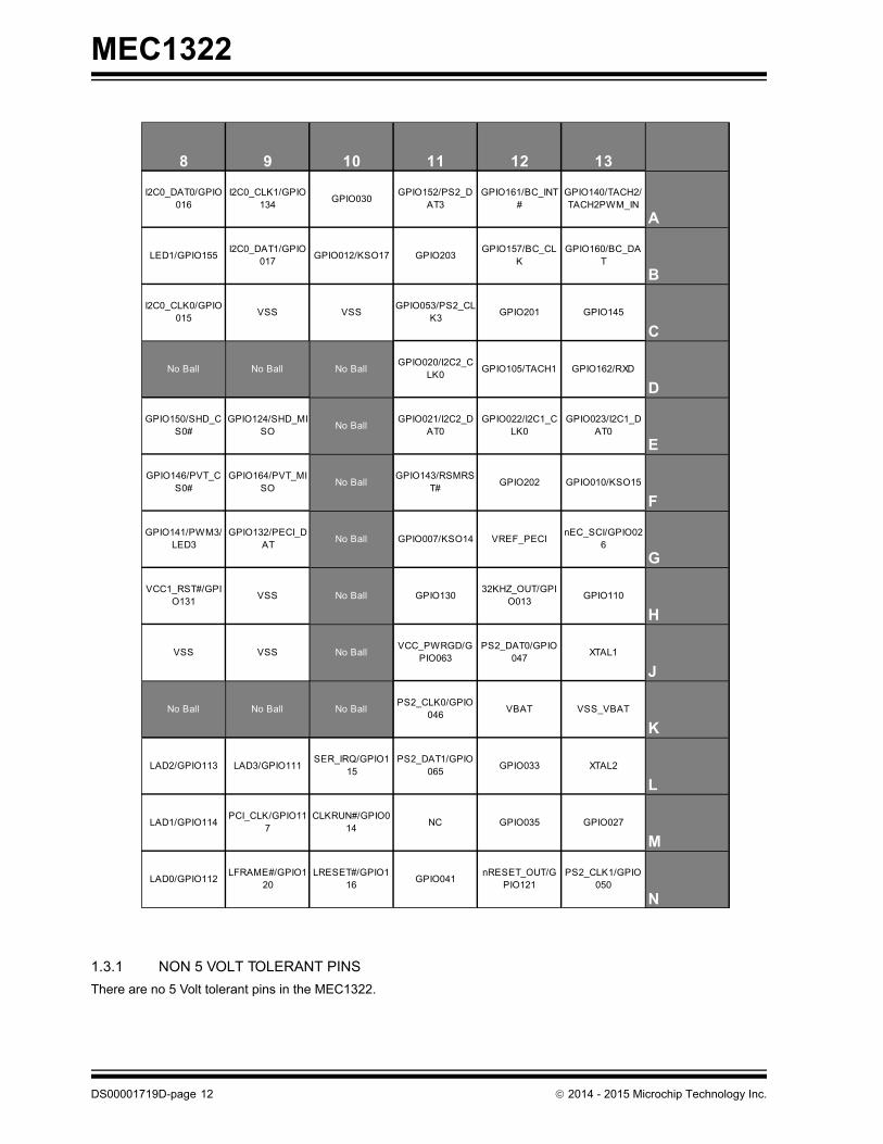
The pin name to package ball mapping of the 144 pin WFBGA package is shown in FIGURE 1-1:
FIGURE 1-1: MEC1322 PIN NAME TO 144-PIN WFBGA BALL MAPPING (TOP)
1 2 3 4 5 6 7
A
KSO13/GPIO006
GPIO011/KSO16
GPIO024/I2C3_CLK0
GPIO135/KBRST VSS GPIO136/PWM1 LED0/GPIO154
B
KSO12/GPIO005
KSO11/GPIO107
GPIO025/I2C3_DAT0
GPIO044/nSMI VSS GPIO133/PWM0 GPIO163
C
KSO09/GPIO106
KSO10/GPIO004
GPIO036 GPIO066GPIO034/PWM2/TACH2PWM_OU
TGPIO204 LED2/GPIO156
DVSS
KSO08/GPIO003
VSS No Ball No Ball No Ball No Ball
E
KSO06/GPIO001
KSO07/GPIO002
VSS No BallGPIO064/SHD_M
OSIGPIO054/PVT_M
OSIGPIO045/A20M/P
VT_CS1#
FCAP GPIO055 VSS No Ball
GPIO153/PVT_SCLK
GPIO122/SHD_SCLK
GPIO165/TXD/SHD_CS1#
GGPIO210
KSO05/GPIO104/TFDP_CLK
GPIO067 No Ball VCC1 VCC1 No Ball
H
KSO03/GPIO102/JTAG_TDO
KSO01/GPIO100/JTAG_TMS
KSO04/GPIO103/TFDP_DATA/XNO
RNo Ball VCC1 VCC1 VCC1
J
KSO02/GPIO101/JTAG_TDI
KSO00/GPIO000/JTAG_TCK
JTAG_RST# No Ball VCC1 VCC1 GPIO123
KKSI7/GPIO043 KSI5/GPIO040 KSI6/GPIO042 No Ball No Ball No Ball No Ball
L
KSI4/GPIO142/TRACECLK
KSI3/GPIO032/TRACEDATA0
KSI2/GPIO144/TRACEDATA1
PS2_CLK2/GPIO051
AVCC ADC1/GPIO057 GPIO200
M
KSI0/GPIO125/TRACEDATA3
KSI1/GPIO126/TRACEDATA2
PS2_DAT2/GPIO052
GPIO151 ADC3/GPIO061 ADC2/GPIO060 AVSS
N
GPIO127/PECI_RDY
GPIO031 GPIO147 GPIO211 ADC4/GPIO062 GPIO206 ADC0/GPIO056
2014 - 2015 Microchip Technology Inc. DS00001719D-page 11
MEC1322
1.3.1 NON 5 VOLT TOLERANT PINS
There are no 5 Volt tolerant pins in the MEC1322.
8 9 10 11 12 13
I2C0_DAT0/GPIO016
I2C0_CLK1/GPIO134
GPIO030GPIO152/PS2_D
AT3GPIO161/BC_INT
#GPIO140/TACH2/TACH2PWM_IN
A
LED1/GPIO155I2C0_DAT1/GPIO
017GPIO012/KSO17 GPIO203
GPIO157/BC_CLK
GPIO160/BC_DAT
B
I2C0_CLK0/GPIO015
VSS VSSGPIO053/PS2_CL
K3GPIO201 GPIO145
C
No Ball No Ball No BallGPIO020/I2C2_C
LK0GPIO105/TACH1 GPIO162/RXD
D
GPIO150/SHD_CS0#
GPIO124/SHD_MISO
No BallGPIO021/I2C2_D
AT0GPIO022/I2C1_C
LK0GPIO023/I2C1_D
AT0
E
GPIO146/PVT_CS0#
GPIO164/PVT_MISO
No BallGPIO143/RSMRS
T#GPIO202 GPIO010/KSO15
F
GPIO141/PWM3/LED3
GPIO132/PECI_DAT
No Ball GPIO007/KSO14 VREF_PECInEC_SCI/GPIO02
6
G
VCC1_RST#/GPIO131
VSS No Ball GPIO13032KHZ_OUT/GPI
O013GPIO110
H
VSS VSS No BallVCC_PWRGD/G
PIO063PS2_DAT0/GPIO
047XTAL1
J
No Ball No Ball No BallPS2_CLK0/GPIO
046VBAT VSS_VBAT
K
LAD2/GPIO113 LAD3/GPIO111SER_IRQ/GPIO1
15PS2_DAT1/GPIO
065GPIO033 XTAL2
L
LAD1/GPIO114PCI_CLK/GPIO11
7CLKRUN#/GPIO0
14NC GPIO035 GPIO027
M
LAD0/GPIO112LFRAME#/GPIO1
20LRESET#/GPIO1
16GPIO041
nRESET_OUT/GPIO121
PS2_CLK1/GPIO050
N
DS00001719D-page 12 2014 - 2015 Microchip Technology Inc.

MEC1322
1.3.2 POR GLITCH PROTECTED PINS
All pins in the MEC1322 have POR output glitch protection. POR output glitch protection ensures that pins will have asteady-state output during VCC1 POR.
In addition, signals in Table 1-4 have additional drive low POR circuitry. Signals in Table 1-4 refer to Pin Reference Num-bers as defined in Table 1-1.
These pins are anti-glitch, driven low on VCC1 POR.
TABLE 1-4: GLITCH PROTECTED POR DRIVE LOW PINS
The following signals require a pull-down on the board:
• nRESET_OUT/GPIO121
• GPIO143/RSMRST#
1.3.3 NON BACKDRIVE PROTECTED PINS
Table 1-5 lists pins which do not have backdrive protection. Signals in Table 1-5 refer to Pin Reference Numbers asdefined in Table 1-1.
These pins have no backdrive protection. If VCC1 is off must insure that none of these pins is above 0V to prevent back-drive onto the VCC1 supply.
Note: The GPIO025/I2C3_DAT0 pin is driven low, glitch free, while VCC1 is coming up. However, after VCC1 isup and stable, the pin becomes an input (i.e., tri-stated Open Drain type), as shown in Table 1-37, “Multi-plexing Table (16 of 18),” on page 36.
Note: These glitch protected pins have no backdrive protection. See Section 1.3.3, "Non Backdrive ProtectedPins".
Pin Reference Number Pin Name
60 nRESET_OUT/GPIO12177 VCC1_RST#/GPIO13185 GPIO143/RSMRST#
125 GPIO025/I2C3_DAT0
2014 - 2015 Microchip Technology Inc. DS00001719D-page 13

MEC1322
TABLE 1-5: NON BACKDRIVE PROTECTED PINS
1.4 Pin Description
1.4.1 OVERVIEW
The following tables describe the signal functions in the MEC1322 pin configuration. See Section 1.6, "Notes for Tablesin this Chapter," on page 39 for notes that are referenced in the Pin Description tables.
1.4.2 HOST INTERFACE
TABLE 1-6: HOST INTERFACE
Pin Reference Number Pin Name
38 ADC4/GPIO06239 ADC3/GPIO06142 ADC2/GPIO06043 ADC1/GPIO05744 ADC0/GPIO05646 LAD0/GPIO11248 LAD1/GPIO11450 LAD2/GPIO11351 LAD3/GPIO11152 LFRAME#/GPIO12053 LRESET#/GPIO11654 PCI_CLK/GPIO11755 CLKRUN#/GPIO01457 SER_IRQ/GPIO11560 nRESET_OUT/GPIO12169 XTAL271 XTAL177 VCC1_RST#/GPIO13179 VREF_PECI80 GPIO132/PECI_DAT85 GPIO143/RSMRST#
125 GPIO025/I2C3_DAT0
HOST INTERFACE (11 Pins)Pin Ref. Number Signal Name Description Notes
57 SER_IRQ Serial IRQ Note 1
53 LRESET#LPC Reset. LRESET# is the same as the system PCI reset, PCIRST#
54 PCI_CLK PCI Clock
52 LFRAME#Frame signal. Indicates start of new cycle and termination of broken cycle
46 LAD0LPC Multiplexed command, address and data bus Bit 0.
Note 1
48 LAD1LPC Multiplexed command, address and data bus Bit 1.
Note 1
50 LAD2LPC Multiplexed command, address and data bus Bit 2.
Note 1
51 LAD3LPC Multiplexed command, address and data bus Bit 3.
Note 1
55 CLKRUN# PCI Clock Control76 nEC_SCI Power Management Event123 nSMI SMI Output
DS00001719D-page 14 2014 - 2015 Microchip Technology Inc.

MEC1322
1.4.3 BC-LINK INTERFACE
TABLE 1-7: BC-LINK INTERFACE
1.4.4 JTAG INTERFACE
TABLE 1-8: JTAG INTERFACE
1.4.5 MASTER CLOCK INTERFACE
TABLE 1-9: MASTER CLOCK INTERFACE
1.4.6 ANALOG DATA ACQUISITION INTERFACE
TABLE 1-10: ANALOG DATA ACQUISITION
Note: JTAG_TDO is a push-pull output. This function is not configured through the associated GPIO Pin ControlRegister; however the drive strength is configured through the associated GPIO Pin Control Register 2.
BC-Link Interface (3 Pins)Pin Ref. Number Signal Name Description Notes
98 BC_CLK BC-Link Master clock 99 BC_DAT BC-Link Master data I/O Note 7100 BC_INT# BC-Link Master interrupt
JTAG Interface (5 Pins)Pin Ref. Number Signal Name Description Notes
21 JTAG_TCK JTAG Test Clock19 JTAG_TDI JTAG Test Data In18 JTAG_TDO JTAG Test Data Out20 JTAG_TMS JTAG Test Mode Select49 JTAG_RST# JTAG Test Reset (active low) Note 2
Master Clock Interface (3 Pins)Pin Ref. Number Signal Name Description Notes
71 XTAL1 32.768 KHz Crystal Output Note 9
69 XTAL232.768 KHz Crystal Input (single-ended 32.768 KHz clock input)
Note 9
75 32KHZ_OUT 32.768 KHz Digital Output
Analog Data Acquisition Interface (5 Pins)Pin Ref. Number Signal Name Description Notes
44 ADC0 ADC channel 0 Note 843 ADC1 ADC channel 1 Note 842 ADC2 ADC channel 2 Note 839 ADC3 ADC channel 3 Note 838 ADC4 ADC channel 4 Note 8
2014 - 2015 Microchip Technology Inc. DS00001719D-page 15

MEC1322
1.4.7 FAN TACHOMETER AND PWM INTERFACE
TABLE 1-11: FAN TACHOMETER AND PWM INTERFACE
1.4.8 GENERAL PURPOSE I/O INTERFACE
TABLE 1-12: GPIO INTERFACE
1.4.9 MISCELLANEOUS FUNCTIONS
TABLE 1-13: MISCELLANEOUS FUNCTIONS
Note 1: The KBRST pin function is the output of CPU_RESET described in Section 11.11.2, "CPU_RESET Hard-ware Speed-Up," on page 151.
2: The nRESET_OUT pin function is an external output signal version of the internal signal nSIO_RESET. Seethe iRESET_OUT bit in the Power Reset Control (PWR_RST_CTRL) Register on page 71 and nSIO_RE-SET in Table 3-7, “Definition of Reset Signals,” on page 52.
3: XNOR is a push-pull output. This function is not configured through the associated GPIO Pin Control Reg-ister; however the drive strength is configured through the associated GPIO Pin Control Register 2.
Note: No GPIO pin should be left floating in a system. If a GPIO pin is not in use, it should be either tied high, tiedlow, or pulled to either power or ground through a resistor.
PWM & TACHOMETER (6 Pins)Pin Ref. Number Signal Name Description Notes
92 TACH1 Fan Tachometer Input 2
101 TACH2PWM_INTach input to RPM-Based Fan Speed ControlAlgorithm
120 PWM0 Pulse Width Modulator Output 0118 PWM1 Pulse Width Modulator Output 178 PWM3 Pulse Width Modulator Output 3
121 TACH2PWM_OUTPulse Width Modulator Output from RPM Based Fan Speed Control Algorithm
GPIO Interface Pin Ref. Number Signal Name Description Notes
See Pin Configuration Table
GPIO General Purpose Input Output Pins Note 12
MISC Functions (13 Pins)Pin Ref. Number Signal Name Description Notes
102 A20M KBD GATEA20 Output122 KBRST CPU_RESET113 LED0 LED (Bllinking/Breathing PWM) Output 0114 LED1 LED (Bllinking/Breathing PWM) Output 1115 LED2 LED (Bllinking/Breathing PWM) Output 278 LED3 LED (Bllinking/Breathing PWM) Output 316 TFDP_CLK Trace FIFO debug port - clock17 TFDP_DATA Trace FIFO debug port - data60 nRESET_OUT EC-driven External System Reset Note 672 VCC_PWRGD System Main Power Indication77 VCC1_RST# Reset Generator Output85 RSMRST# Resume Reset Output Note 617 XNOR Test Output
DS00001719D-page 16 2014 - 2015 Microchip Technology Inc.
MEC1322
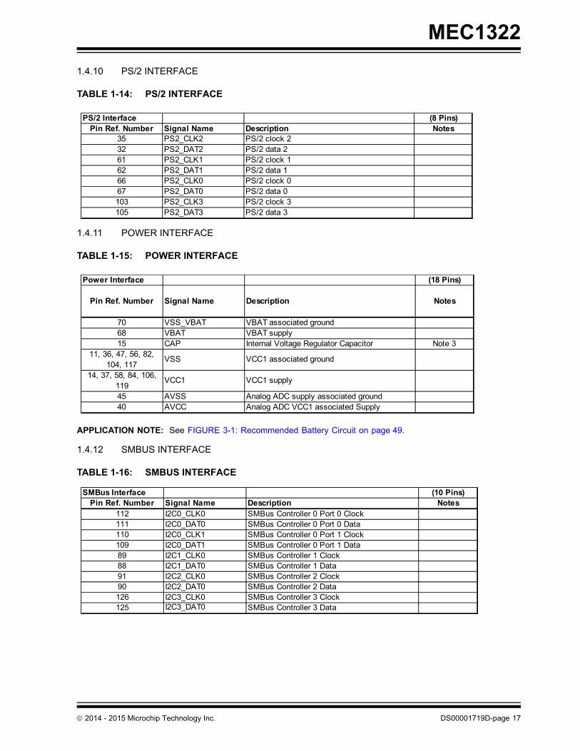
1.4.10 PS/2 INTERFACE
TABLE 1-14: PS/2 INTERFACE
1.4.11 POWER INTERFACE
TABLE 1-15: POWER INTERFACE
APPLICATION NOTE: See FIGURE 3-1: Recommended Battery Circuit on page 49.
1.4.12 SMBUS INTERFACE
TABLE 1-16: SMBUS INTERFACE
PS/2 Interface (8 Pins)Pin Ref. Number Signal Name Description Notes
35 PS2_CLK2 PS/2 clock 232 PS2_DAT2 PS/2 data 261 PS2_CLK1 PS/2 clock 162 PS2_DAT1 PS/2 data 166 PS2_CLK0 PS/2 clock 067 PS2_DAT0 PS/2 data 0103 PS2_CLK3 PS/2 clock 3105 PS2_DAT3 PS/2 data 3
Power Interface (18 Pins)
Pin Ref. Number Signal Name Description Notes
70 VSS_VBAT VBAT associated ground68 VBAT VBAT supply 15 CAP Internal Voltage Regulator Capacitor Note 3
11, 36, 47, 56, 82, 104, 117
VSS VCC1 associated ground
14, 37, 58, 84, 106, 119
VCC1 VCC1 supply
45 AVSS Analog ADC supply associated ground40 AVCC Analog ADC VCC1 associated Supply
SMBus Interface (10 Pins)Pin Ref. Number Signal Name Description Notes
112 I2C0_CLK0 SMBus Controller 0 Port 0 Clock111 I2C0_DAT0 SMBus Controller 0 Port 0 Data110 I2C0_CLK1 SMBus Controller 0 Port 1 Clock109 I2C0_DAT1 SMBus Controller 0 Port 1 Data89 I2C1_CLK0 SMBus Controller 1 Clock88 I2C1_DAT0 SMBus Controller 1 Data91 I2C2_CLK0 SMBus Controller 2 Clock90 I2C2_DAT0 SMBus Controller 2 Data126 I2C3_CLK0 SMBus Controller 3 Clock125 I2C3_DAT0 SMBus Controller 3 Data
2014 - 2015 Microchip Technology Inc. DS00001719D-page 17

MEC1322
1.4.13 PECI INTERFACE
TABLE 1-17: PECI INTERFACE
1.4.14 KEYBOARD SCAN INTERFACE
TABLE 1-18: KEYBOARD SCAN INTERFACE
PECI Interface (3 Pins)Pin Ref. Number Signal Name Description Notes
80 PECI_DAT PECI Bus31 PECI_RDY PECI Ready79 VREF_PECI PECI Voltage Reference
Keyboard Scan Interface (26 Pins)Pin Ref. Number Signal Name Description Notes
29 KSI0 Keyboard Scan Matrix Input 0 Note 1128 KSI1 Keyboard Scan Matrix Input 1 Note 1127 KSI2 Keyboard Scan Matrix Input 2 Note 1126 KSI3 Keyboard Scan Matrix Input 3 Note 1125 KSI4 Keyboard Scan Matrix Input 4 Note 1124 KSI5 Keyboard Scan Matrix Input 5 Note 1123 KSI6 Keyboard Scan Matrix Input 6 Note 1122 KSI7 Keyboard Scan Matrix Input 7 Note 1121 KSO00 Keyboard Scan Matrix Output 020 KSO01 Keyboard Scan Matrix Output 119 KSO02 Keyboard Scan Matrix Output 218 KSO03 Keyboard Scan Matrix Output 317 KSO04 Keyboard Scan Matrix Output 416 KSO05 Keyboard Scan Matrix Output 513 KSO06 Keyboard Scan Matrix Output 612 KSO07 Keyboard Scan Matrix Output 710 KSO08 Keyboard Scan Matrix Output 89 KSO09 Keyboard Scan Matrix Output 98 KSO10 Keyboard Scan Matrix Output 107 KSO11 Keyboard Scan Matrix Output 116 KSO12 Keyboard Scan Matrix Output 125 KSO13 Keyboard Scan Matrix Output 13
81 KSO14 Keyboard Scan Matrix Output 1483 KSO15 Keyboard Scan Matrix Output 154 KSO16 Keyboard Scan Matrix Output 16
108 KSO17 Keyboard Scan Matrix Output 17
DS00001719D-page 18 2014 - 2015 Microchip Technology Inc.

MEC1322
1.4.15 SPI CONTROLLER INTERFACE
TABLE 1-19: SPI CONTROLLER INTERFACE
1.4.16 TRACE DEBUG INTERFACE
TABLE 1-20: TRACE DEBUG INTERFACE
The Trace Debug Interface is enabled using the TRACE_EN bit in the ETM TRACE Enable register defined in Chapter35.0, "EC Subsystem Registers".
1.4.17 UART PORT
TABLE 1-21: UART PORT
1.5 Pin Multiplexing
Multifunction Pin Multiplexing in the MEC1322 is controlled by the GPIO Interface and illustrated in the MultiplexingTables that follow. See Section 1.6, "Notes for Tables in this Chapter," on page 39 for notes that are referenced in thePin Multiplexing tables. See Section 20.8.1, "Pin Control Register," on page 250 for Pin Multiplexing programmingdetails. See also Section 20.7, "Pin Multiplexing Control," on page 248.
Pin signal functions that exhibit power domain emulation (see Multiplexing Tables below) have a different power supplydesignation in the “Emulated Power Well” column and “Signal Power Well“ columns of the Multiplexing Tables inSection 1.5.2.
Note: These pins are push-pull outputs when enabled as the Trace Debug Interface pin functions. This function-ality is not configured through the associated GPIO Pin Control Register; however the drive strength ofthese pins is configured through the associated GPIO Pin Control Register 2.
SPI Controllers Interface (10 Pins)Pin Ref. Number Signal Name Description Notes
3 SHD_SCLK Shared SPI Clock Note 10128 SHD_MOSI Shared SPI Output Note 1095 SHD_MISO Shared SPI Input Note 1097 SHD_CS0# Shared SPI Chip Select 0 Note 1087 SHD_CS1# Shared SPI Chip Select 12 PVT_SCLK Private SPI Clock Note 10
127 PVT_MOSI Private SPI Output Note 1094 PVT_MISO Private SPI Input Note 1096 PVT_CS0# Private SPI Chip Select 0 Note 10102 PVT_CS1# Private SPI Chip Select 1
Trace Debug Interface (5 Pins)Pin Ref. Number Signal Name Description Notes
25 TRACECLK Trace Clock26 TRACEDATA0 Trace Data 027 TRACEDATA1 Trace Data 128 TRACEDATA2 Trace Data 229 TRACEDATA3 Trace Data 3
UART Port (2 Pins)Pin Ref. Number Signal Name Description Notes
86 RXD UART Receive Data87 TXD UART Transmit Data
2014 - 2015 Microchip Technology Inc. DS00001719D-page 19

MEC1322
1.5.1 VCC2 POWER DOMAIN EMULATION
The System Runtime Supply power VCC2 is not connected to the MEC1322. The VCC_PWRGD signal is used to indi-cate when power is applied to the System Runtime Supply.
Pin signal functions with VCC2 power domain emulation are documented in the Multiplexing Tables as “Signal PowerWell“= VCC1 and “Emulated Power Well” = VCC2. These pins are powered by VCC1 and controlled by the VCC_P-WRGD signal input. Outputs on VCC2 power domain emulation pin signal functions are tri-stated when VCC_PWRGDis not asserted and are functional when VCC_PWRGD is active. Inputs on VCC2 power domain emulation pin signalfunctions are gated according as defined by the Gated State column in the following tables.
Power well emulation for GPIOs and for signals that are multiplexed with GPIO signals is controlled by the Power GatingSignals field in the GPIO Pin Control Register.
1.5.2 MULTIPLEXING TABLES
In the following tables, the columns have the following meanings:
MUX
If the pin has an associated GPIO, then the MUX column refers to the Mux Control field in the GPIO Pin Control Register.Setting the Mux Control field to value listed in the row will configure the pin for the signal listed in the Signal column onthe same row. The row marked “Default” is the setting that is assigned on system reset.
If there is no GPIO associated with a pin, then the pin has a single function.
Signal
This column lists the signals that can appear on each pin, as configured by the MUX control.
Buffer Type
Pin buffer types are defined in Table 37-4, “DC Electrical Characteristics,” on page 391.
Note that all GPIO pins are of buffer type PIO, which may be configured as input/output, push-pull/OD etc. via the GPIOPin Control Register and Pin Control Register 2. There are some pins where the buffer type is configured by the alternatefunction selection, in which case that buffer type is shown in this column.
Default Operation
This column gives the pin behavior following the power-up of VCC1. All GPIO pins are programmable after this event.This default pin behavior corresponds to the row marked “Default” in the MUX column.
Signal Power Well
This column defines the power well that powers the pin.
Emulated Power Well
Power well emulation for GPIOs and for signals that are multiplexed with GPIO signals is controlled by the Power GatingSignals field in the GPIO Pin Control Register.
Power well emulation for signals that are not multiplexed with GPIO signals is defined by the entries in this column.
See Section 1.5.1, "VCC2 Power Domain Emulation".
Gated State
This column defines the internal value of an input signal when either its emulated power well is inactive or it is notselected by the GPIO alternate function MUX. A value of “No Gate” means that the internal signal always follows thepin even when the emulated power well is inactive.
Note: An internal pull-up resistor is indicated by (PU) and and internal pull-down is indicated by (PD). These areconfigured via the GPIO Pin Control Register.
Note: The Glitch Protected POR Drive Low Pins are configured as “always on”, as indicated by “ON” in this col-umn.
Note: Gated state is only meaningful to the operation of input signals. A gated state on an output pin defines theinternal behavior of the GPIO MUX and does not imply pin behavior.
DS00001719D-page 20 2014 - 2015 Microchip Technology Inc.

MEC1322
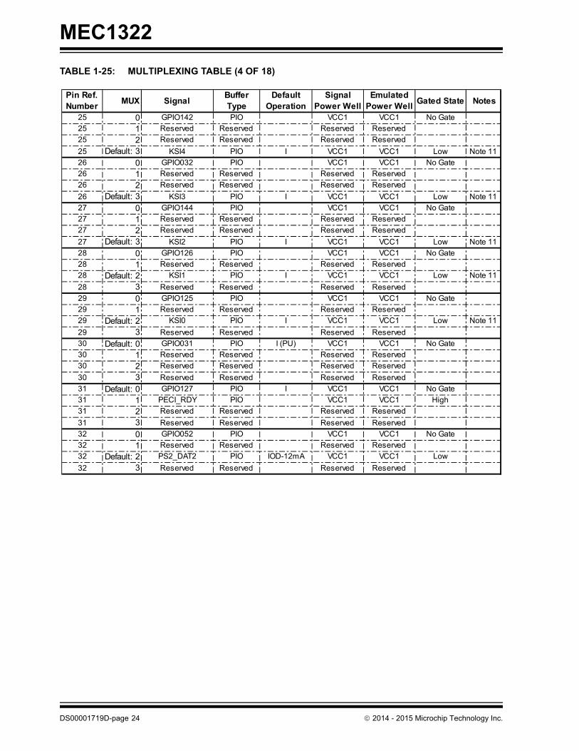
TABLE 1-22: MULTIPLEXING TABLE (1 OF 18)
Pin Ref. Number
MUX SignalBuffer Type
Default Operation
Signal Power Well
Emulated Power Well
Gated State Notes
1 Default: 0 GPIO036 PIO I (PU) VCC1 VCC1 No Gate
1 1 Reserved Reserved Reserved Reserved
1 2 Reserved Reserved Reserved Reserved
1 3 Reserved Reserved Reserved Reserved
2 Default: 0 GPIO153 PIO I VCC1 VCC1 No Gate Note 10
2 1 PVT_SCLK PIO VCC1 VCC1 Note 10
2 2 Reserved Reserved Reserved Reserved
2 3 Reserved Reserved Reserved Reserved
3 Default: 0 GPIO122 PIO I (PD) VCC1 VCC1 No Gate Note 10
3 1 SHD_SCLK PIO VCC1 VCC1 Note 10
3 2 Reserved Reserved Reserved Reserved
3 3 Reserved Reserved Reserved Reserved
4 Default: 0 GPIO011 PIO IOD (PD) VCC1 VCC1 No Gate
4 1 Reserved Reserved Reserved Reserved
4 2 Reserved Reserved Reserved Reserved
4 3 KSO16 PIO VCC1 VCC1
5 0 GPIO006 PIO VCC1 VCC1 No Gate
5 1 Reserved Reserved Reserved Reserved
5 2 Reserved Reserved Reserved Reserved
5 Default: 3 KSO13 PIO O-4mA VCC1 VCC1
6 0 GPIO005 PIO VCC1 VCC1 No Gate
6 1 Reserved Reserved Reserved Reserved
6 2 Reserved Reserved Reserved Reserved
6 Default: 3 KSO12 PIO O-4mA (PD) VCC1 VCC1
7 0 GPIO107 PIO VCC1 VCC1 No Gate
7 1 Reserved Reserved Reserved Reserved
7 2 Reserved Reserved Reserved Reserved
7 Default: 3 KSO11 PIO O-4mA VCC1 VCC1
8 0 GPIO004 PIO VCC1 VCC1 No Gate
8 1 Reserved Reserved Reserved Reserved
8 2 Reserved Reserved Reserved Reserved
8 Default: 3 KSO10 PIO O-4mA VCC1 VCC1
2014 - 2015 Microchip Technology Inc. DS00001719D-page 21

MEC1322
TABLE 1-23: MULTIPLEXING TABLE (2 OF 18)
Pin Ref. Number
MUX SignalBuffer Type
Default Operation
Signal Power Well
Emulated Power Well
Gated State Notes
9 0 GPIO106 PIO VCC1 VCC1 No Gate
9 1 Reserved Reserved Reserved Reserved
9 2 Reserved Reserved Reserved Reserved
9 Default: 3 KSO09 PIO O-4mA VCC1 VCC1
10 0 GPIO003 PIO VCC1 VCC1 No Gate
10 1 Reserved Reserved Reserved Reserved
10 2 Reserved Reserved Reserved Reserved
10 Default: 3 KSO08 PIO O-4mA VCC1 VCC1
11 VSS PWR PWR PWR
11
11
11
12 0 GPIO002 PIO VCC1 VCC1 No Gate
12 1 Reserved Reserved Reserved Reserved
12 2 Reserved Reserved Reserved Reserved
12 Default: 3 KSO07 PIO O-4mA VCC1 VCC1
13 0 GPIO001 PIO VCC1 VCC1 No Gate
13 1 Reserved Reserved Reserved Reserved
13 2 Reserved Reserved Reserved Reserved
13 Default: 3 KSO06 PIO O-4mA VCC1 VCC1
14 VCC1 PWR PWR PWR
14
14
14
15 CAP PWR PWR PWR Note 3
15
15
15
16 0 GPIO104 PIO VCC1 VCC1 No Gate
16 1 TFDP_CLK PIO VCC1 VCC1
16 2 Reserved Reserved Reserved Reserved
16 Default: 3 KSO05 PIO O-4mA VCC1 VCC1
DS00001719D-page 22 2014 - 2015 Microchip Technology Inc.

MEC1322
TABLE 1-24: MULTIPLEXING TABLE (3 OF 18)
Pin Ref. Number
MUX SignalBuffer Type
Default Operation
Signal Power Well
Emulated Power Well
Gated State Notes
17 0 GPIO103 PIO VCC1 VCC1 No Gate
17 1 TFDP_DATA PIO VCC1 VCC1
17 2 Reserved Reserved Reserved Reserved
17 Default: 3 KSO04 PIO O-4mA VCC1 VCC1
18 0 GPIO102 PIO VCC1 VCC1 No Gate
18 1 Reserved Reserved Reserved Reserved
18 2 Reserved Reserved Reserved Reserved
18 Default: 3 KSO03 PIO O-4mA VCC1 VCC1
19 0 GPIO101 PIO VCC1 VCC1 No Gate
19 1 Reserved Reserved Reserved Reserved
19 2 Reserved Reserved Reserved Reserved
19 Default: 3 KSO02 PIO O-4mA VCC1 VCC1
20 0 GPIO100 PIO VCC1 VCC1 No Gate
20 1 Reserved Reserved Reserved Reserved
20 2 Reserved Reserved Reserved Reserved
20 Default: 3 KSO01 PIO O-4mA VCC1 VCC1
21 0 GPIO000 PIO VCC1 VCC1 No Gate
21 1 Reserved Reserved Reserved Reserved
21 2 Reserved Reserved Reserved Reserved
21 Default: 3 KSO00 PIO O-4mA VCC1 VCC1
22 0 GPIO043 PIO VCC1 VCC1 No Gate
22 1 Reserved Reserved Reserved Reserved
22 2 Reserved Reserved Reserved Reserved
22 Default: 3 KSI7 PIO I VCC1 VCC1 Low Note 11
23 0 GPIO042 PIO VCC1 VCC1 No Gate
23 1 Reserved Reserved Reserved Reserved
23 2 Reserved Reserved Reserved Reserved
23 Default: 3 KSI6 PIO I VCC1 VCC1 Low Note 11
24 0 GPIO040 PIO VCC1 VCC1 No Gate
24 1 Reserved Reserved Reserved Reserved
24 2 Reserved Reserved Reserved Reserved
24 Default: 3 KSI5 PIO I VCC1 VCC1 Low Note 11
2014 - 2015 Microchip Technology Inc. DS00001719D-page 23
MEC1322
TABLE 1-25: MULTIPLEXING TABLE (4 OF 18)
Pin Ref. Number
MUX SignalBuffer Type
Default Operation
Signal Power Well
Emulated Power Well
Gated State Notes
25 0 GPIO142 PIO VCC1 VCC1 No Gate
25 1 Reserved Reserved Reserved Reserved
25 2 Reserved Reserved Reserved Reserved
25 Default: 3 KSI4 PIO I VCC1 VCC1 Low Note 11
26 0 GPIO032 PIO VCC1 VCC1 No Gate
26 1 Reserved Reserved Reserved Reserved
26 2 Reserved Reserved Reserved Reserved
26 Default: 3 KSI3 PIO I VCC1 VCC1 Low Note 11
27 0 GPIO144 PIO VCC1 VCC1 No Gate
27 1 Reserved Reserved Reserved Reserved
27 2 Reserved Reserved Reserved Reserved
27 Default: 3 KSI2 PIO I VCC1 VCC1 Low Note 11
28 0 GPIO126 PIO VCC1 VCC1 No Gate
28 1 Reserved Reserved Reserved Reserved
28 Default: 2 KSI1 PIO I VCC1 VCC1 Low Note 11
28 3 Reserved Reserved Reserved Reserved
29 0 GPIO125 PIO VCC1 VCC1 No Gate
29 1 Reserved Reserved Reserved Reserved
29 Default: 2 KSI0 PIO I VCC1 VCC1 Low Note 11
29 3 Reserved Reserved Reserved Reserved
30 Default: 0 GPIO031 PIO I (PU) VCC1 VCC1 No Gate
30 1 Reserved Reserved Reserved Reserved
30 2 Reserved Reserved Reserved Reserved
30 3 Reserved Reserved Reserved Reserved
31 Default: 0 GPIO127 PIO I VCC1 VCC1 No Gate
31 1 PECI_RDY PIO VCC1 VCC1 High
31 2 Reserved Reserved Reserved Reserved
31 3 Reserved Reserved Reserved Reserved
32 0 GPIO052 PIO VCC1 VCC1 No Gate
32 1 Reserved Reserved Reserved Reserved
32 Default: 2 PS2_DAT2 PIO IOD-12mA VCC1 VCC1 Low
32 3 Reserved Reserved Reserved Reserved
DS00001719D-page 24 2014 - 2015 Microchip Technology Inc.

MEC1322
TABLE 1-26: MULTIPLEXING TABLE (5 OF 18)
Pin Ref. Number
MUX SignalBuffer Type
Default Operation
Signal Power Well
Emulated Power Well
Gated State Notes
33 Default: 0 GPIO147 PIO I (PU) VCC1 VCC1 No Gate
33 1 Reserved Reserved Reserved Reserved
33 2 Reserved Reserved Reserved Reserved
33 3 Reserved Reserved Reserved Reserved
34 Default: 0 GPIO151 PIO I (PU) VCC1 VCC1 No Gate
34 1 Reserved Reserved Reserved Reserved
34 2 Reserved Reserved Reserved Reserved
34 3 Reserved Reserved Reserved Reserved
35 0 GPIO051 PIO VCC1 VCC1 No Gate
35 1 Reserved Reserved Reserved Reserved
35 Default: 2 PS2_CLK2 PIO IOD-12mA VCC1 VCC1 Low
35 3 Reserved Reserved Reserved Reserved
36 VSS PWR PWR PWR
36
36
36
37 VCC1 PWR PWR PWR
37
37
37
38 0 GPIO062 PIO VCC1 VCC1 No Gate
38 Default: 1 ADC4 I_AN I_AN AVCC1_ADC AVCC1_ADC Low Note 8
38 2 Reserved Reserved Reserved Reserved
38 3 Reserved Reserved Reserved Reserved
39 0 GPIO061 PIO VCC1 VCC1 No Gate
39 Default: 1 ADC3 I_AN I_AN AVCC1_ADC AVCC1_ADC Low Note 8
39 2 Reserved Reserved Reserved Reserved
39 3 Reserved Reserved Reserved Reserved
40 AVCC PWR PWR PWR
40
40
40
2014 - 2015 Microchip Technology Inc. DS00001719D-page 25

MEC1322
TABLE 1-27: MULTIPLEXING TABLE (6 OF 18)
Pin Ref. Number
MUX SignalBuffer Type
Default Operation
Signal Power Well
Emulated Power Well
Gated State Notes
41 Default: 0 GPIO206 PIO I VCC1 VCC1 No Gate
41 1 Reserved Reserved Reserved Reserved
41 2 Reserved Reserved Reserved Reserved
41 3 Reserved Reserved Reserved Reserved
42 0 GPIO060 PIO VCC1 VCC1 No Gate
42 Default: 1 ADC2 I_AN I_AN (PU) AVCC1_ADC AVCC1_ADC Low Note 8
42 2 Reserved Reserved Reserved Reserved
42 3 Reserved Reserved Reserved Reserved
43 0 GPIO057 PIO VCC1 VCC1 No Gate
43 Default: 1 ADC1 I_AN I_AN AVCC1_ADC AVCC1_ADC Low Note 8
43 2 Reserved Reserved Reserved Reserved
43 3 Reserved Reserved Reserved Reserved
44 0 GPIO056 PIO VCC1 VCC1 No Gate
44 1 ADC0 I_AN AVCC1_ADC AVCC1_ADC Low Note 8
44 2 Reserved Reserved Reserved Reserved
44 Default: 3 ADC0 I_AN I_AN AVCC1_ADC AVCC1_ADC Low Note 8
45 AVSS PWR PWR PWR
45
45
45
46 0 GPIO112 PCI_PIO VCC1 VCC1 No Gate
46 Default: 1 LAD0 PCI_IO PCI_IO VCC1 VCC1 High Note 1
46 2 Reserved Reserved Reserved Reserved
46 3 Reserved Reserved Reserved Reserved
47 VSS PWR PWR PWR
47
47
47
48 0 GPIO114 PCI_PIO VCC1 VCC1 No Gate
48 Default: 1 LAD1 PCI_IO PCI_IO VCC1 VCC1 High Note 1
48 2 Reserved Reserved Reserved Reserved
48 3 Reserved Reserved Reserved Reserved
DS00001719D-page 26 2014 - 2015 Microchip Technology Inc.

MEC1322
TABLE 1-28: MULTIPLEXING TABLE (7 OF 18)
Pin Ref. Number
MUX SignalBuffer Type
Default Operation
Signal Power Well
Emulated Power Well
Gated State Notes
49 Default: 0 JTAG_RST# I I VCC1 VCC1 No Gate Note 2
49 1 Reserved Reserved Reserved Reserved
49 2 Reserved Reserved Reserved Reserved
49 3 Reserved Reserved Reserved Reserved
50 0 GPIO113 PCI_PIO VCC1 VCC1 No Gate
50 Default: 1 LAD2 PCI_IO PCI_IO VCC1 VCC1 High Note 1
50 2 Reserved Reserved Reserved Reserved
50 3 Reserved Reserved Reserved Reserved
51 0 GPIO111 PCI_PIO VCC1 VCC1 No Gate
51 Default: 1 LAD3 PCI_IO PCI_IO VCC1 VCC1 High Note 1
51 2 Reserved Reserved Reserved Reserved
51 3 Reserved Reserved Reserved Reserved
52 0 GPIO120 PCI_PIO VCC1 VCC1 No Gate
52 Default: 1 LFRAME# PCI_I PCI_I VCC1 VCC1 High
52 2 Reserved Reserved Reserved Reserved
52 3 Reserved Reserved Reserved Reserved
53 0 GPIO116 PCI_PIO VCC1 VCC1 No Gate
53 Default: 1 LRESET# PCI_I PCI_I VCC1 VCC1 Low
53 2 Reserved Reserved Reserved Reserved
53 3 Reserved Reserved Reserved Reserved
54 0 GPIO117 PCI_PIO VCC1 VCC1 No Gate
54 Default: 1 PCI_CLK PCI_CLK PCI_CLK VCC1 VCC1 Low
54 2 Reserved Reserved Reserved Reserved
54 3 Reserved Reserved Reserved Reserved
55 0 GPIO014 PCI_PIO VCC1 VCC1 No Gate
55 Default: 1 CLKRUN# PCI_I PCI_I VCC1 VCC1 Low
55 2 Reserved Reserved Reserved Reserved
55 3 Reserved Reserved Reserved Reserved
56 VSS PWR PWR PWR
56
56
56
2014 - 2015 Microchip Technology Inc. DS00001719D-page 27

MEC1322
TABLE 1-29: MULTIPLEXING TABLE (8 OF 18)
Pin Ref. Number
MUX SignalBuffer Type
Default Operation
Signal Power Well
Emulated Power Well
Gated State Notes
57 0 GPIO115 PCI_PIO VCC1 VCC1 No Gate
57 Default: 1 SER_IRQ PCI_I PCI_I VCC1 VCC1 High Note 1
57 2 Reserved Reserved Reserved Reserved
57 3 Reserved Reserved Reserved Reserved
58 VCC1 PWR PWR PWR
58
58
58
59 0 GPIO041 PIO VCC1 VCC1 No Gate
59 Default: 1 Reserved PIOO-8mA (PD)
LOWVCC1 ON Note 12
59 2 Reserved Reserved Reserved Reserved
59 3 Reserved Reserved Reserved Reserved
60 0 GPIO121 PIO VCC1 VCC1 No Gate
60 Default: 1 nRESET_OUT PIO O-8mA VCC1 ON Note 6
60 2 Reserved Reserved Reserved Reserved
60 3 Reserved Reserved Reserved Reserved
61 0 GPIO050 PIO VCC1 VCC1 No Gate
61 1 Reserved Reserved Reserved Reserved
61 Default: 2 PS2_CLK1 PIO IOD-12mA VCC1 VCC1 Low
61 3 Reserved Reserved Reserved Reserved
62 0 GPIO065 PIO VCC1 VCC1 No Gate
62 1 Reserved Reserved Reserved Reserved
62 Default: 2 PS2_DAT1 PIO IOD-12mA VCC1 VCC1 Low
62 3 Reserved Reserved Reserved Reserved
63 Default: 0 GPIO035 PIO I (PU) VCC1 VCC1 No Gate
63 1 Reserved Reserved Reserved Reserved
63 2 Reserved Reserved Reserved Reserved
63 3 Reserved Reserved Reserved Reserved
64 Default: 0 GPIO027 PIO I (PU) VCC1 VCC1 No Gate
64 1 Reserved Reserved Reserved Reserved
64 2 Reserved Reserved Reserved Reserved
64 3 Reserved Reserved Reserved Reserved
DS00001719D-page 28 2014 - 2015 Microchip Technology Inc.

MEC1322
TABLE 1-30: MULTIPLEXING TABLE (9 OF 18)
Pin Ref. Number
MUX SignalBuffer Type
Default Operation
Signal Power Well
Emulated Power Well
Gated State Notes
65 Default: 0 GPIO033 PIO I (PU) VCC1 VCC1 No Gate
65 1 Reserved Reserved Reserved Reserved
65 2 Reserved Reserved Reserved Reserved
65 3 Reserved Reserved Reserved Reserved
66 0 GPIO046 PIO VCC1 VCC1 No Gate
66 1 Reserved Reserved Reserved Reserved
66 Default: 2 PS2_CLK0 PIO IOD-12mA VCC1 VCC1 Low
66 3 Reserved Reserved Reserved Reserved
67 0 GPIO047 PIO VCC1 VCC1 No Gate
67 1 Reserved Reserved Reserved Reserved
67 Default: 2 PS2_DAT0 PIO IOD-12mA VCC1 VCC1 Low
67 3 Reserved Reserved Reserved Reserved
68 VBAT PWR PWR PWR
68
68
68
69 Default: 0 XTAL2 ICLK VBAT VBAT Note 9
69 1 Reserved Reserved Reserved Reserved
69 2 Reserved Reserved Reserved Reserved
69 3 Reserved Reserved Reserved Reserved
70 VSS_VBAT PWR PWR PWR
70
70
70
71 Default: 0 XTAL1 OCLK VBAT VBAT Note 9
71 1 Reserved Reserved Reserved Reserved
71 2 Reserved Reserved Reserved Reserved
71 3 Reserved Reserved Reserved Reserved
72 0 GPIO063 PIO VCC1 VCC1 No Gate
72 Default: 1 VCC_PWRGD PIO I VCC1 VCC1 High
72 2 Reserved Reserved Reserved Reserved
72 3 Reserved Reserved Reserved Reserved
2014 - 2015 Microchip Technology Inc. DS00001719D-page 29

MEC1322
TABLE 1-31: MULTIPLEXING TABLE (10 OF 18)
Pin Ref. Number
MUX SignalBuffer Type
Default Operation
Signal Power Well
Emulated Power Well
Gated State Notes
73 Default: 0 GPIO110 PIO I VCC1 VCC1 No Gate
73 1 Reserved Reserved Reserved Reserved
73 2 Reserved Reserved Reserved Reserved
73 3 Reserved Reserved Reserved Reserved
74 Default: 0 GPIO130 PIO I VCC1 VCC1 No Gate
74 1 Reserved Reserved Reserved Reserved
74 2 Reserved Reserved Reserved Reserved
74 3 Reserved Reserved Reserved Reserved
75 0 GPIO013 PIO VCC1 VCC1 No Gate
75 1 Reserved Reserved Reserved Reserved
75 Default: 2 32KHZ_OUT PIO O-4mA VCC1 VCC1
75 3 Reserved Reserved Reserved Reserved
76 0 GPIO026 PIO VCC1 VCC1 No Gate
76 1 Reserved Reserved Reserved Reserved
76 Default: 2 nEC_SCI PIO OD-12mA VCC1 VCC1
76 3 Reserved Reserved Reserved Reserved
77 0 GPIO131 PIO VCC1 VCC1 No Gate
77 Default: 1 VCC1_RST# PIO OD-4mA VCC1 ON High
77 2 Reserved Reserved Reserved Reserved
77 3 Reserved Reserved Reserved Reserved
78 Default: 0 GPIO141 PIO I VCC1 VCC1 No Gate
78 1 PWM3 PIO VCC1 VCC1
78 2 LED3 PIO VCC1 VCC1
78 3 Reserved Reserved Reserved Reserved
79 VREF_PECI VREF_PECI VREF_PECI VREF_PECI
79
79
79
80 Default: 0 GPIO132 PIO I VCC1 VCC1 No Gate
80 1 PECI_DAT PECI_IO VREF_PECI VREF_PECI Low
80 2 Reserved Reserved Reserved Reserved
80 3 Reserved Reserved Reserved Reserved
DS00001719D-page 30 2014 - 2015 Microchip Technology Inc.

MEC1322
TABLE 1-32: MULTIPLEXING TABLE (11 OF 18)
Pin Ref. Number
MUX SignalBuffer Type
Default Operation
Signal Power Well
Emulated Power Well
Gated State Notes
81 Default: 0 GPIO007 PIO I VCC1 VCC1 No Gate
81 1 Reserved Reserved Reserved Reserved
81 2 Reserved Reserved Reserved Reserved
81 3 KSO14 PIO VCC1 VCC1
82 VSS PWR PWR PWR
82
82
82
83 Default: 0 GPIO010 PIO I VCC1 VCC1 No Gate
83 1 Reserved Reserved Reserved Reserved
83 2 Reserved Reserved Reserved Reserved
83 3 KSO15 PIO VCC1 VCC1
84 VCC1 PWR PWR PWR
84
84
84
85 Default: 0 GPIO143 PIO I VCC1 ON No Gate
85 1 RSMRST# PIO VCC1 VCC1 Note 6
85 2 Reserved Reserved Reserved Reserved
85 3 Reserved Reserved Reserved Reserved
86 Default: 0 GPIO162 PIO I VCC1 VCC1 No Gate
86 1 RXD PIO VCC1 VCC1 High
86 2 Reserved Reserved Reserved Reserved
86 3 Reserved Reserved Reserved Reserved
87 Default: 0 GPIO165 PIO I VCC1 VCC1 No Gate
87 1 TXD PIO VCC1 VCC1 High
87 2 SHD_CS1# PIO VCC1 VCC1 High
87 3 Reserved Reserved Reserved Reserved
88 Default: 0 GPIO023 PIO I VCC1 VCC1 No Gate Note 5
88 1 Reserved Reserved Reserved Reserved
88 2 I2C1_DAT0 PIO VCC1 VCC1 High
88 3 Reserved Reserved Reserved Reserved
2014 - 2015 Microchip Technology Inc. DS00001719D-page 31

MEC1322
TABLE 1-33: MULTIPLEXING TABLE (12 OF 18)
Pin Ref. Number
MUX SignalBuffer Type
Default Operation
Signal Power Well
Emulated Power Well
Gated State Notes
89 Default: 0 GPIO022 PIO I VCC1 VCC1 No Gate Note 5
89 1 Reserved Reserved Reserved Reserved
89 2 I2C1_CLK0 PIO VCC1 VCC1 High
89 3 Reserved Reserved Reserved Reserved
90 Default: 0 GPIO021 PIO I VCC1 VCC1 No Gate
90 1 Reserved Reserved Reserved Reserved
90 2 I2C2_DAT0 PIO VCC1 VCC1 High
90 3 Reserved Reserved Reserved Reserved
91 Default: 0 GPIO020 PIO I VCC1 VCC1 No Gate
91 1 Reserved Reserved Reserved Reserved
91 2 I2C2_CLK0 PIO VCC1 VCC1 High
91 3 Reserved Reserved Reserved Reserved
92 Default: 0 GPIO105 PIO I VCC1 VCC1 No Gate
92 1 TACH1 PIO VCC1 VCC1 Low
92 2 Reserved Reserved Reserved Reserved
92 3 Reserved Reserved Reserved Reserved
93 Default: 0 GPIO145 PIO I (PU) VCC1 VCC1 No Gate
93 1 Reserved Reserved Reserved Reserved
93 2 Reserved Reserved Reserved Reserved
93 3 Reserved Reserved Reserved Reserved
94 Default: 0 GPIO164 PIO I VCC1 VCC1 No Gate Note 10
94 1 PVT_MISO PIO VCC1 VCC1 Low Note 10
94 2 Reserved Reserved Reserved Reserved
94 3 Reserved Reserved Reserved Reserved
95 Default: 0 GPIO124 PIO I VCC1 VCC1 No Gate Note 10
95 1 SHD_MISO PIO VCC1 VCC1 Low Note 10
95 2 Reserved Reserved Reserved Reserved
95 3 Reserved Reserved Reserved Reserved
96 Default: 0 GPIO146 PIO I VCC1 VCC1 No GateNote 4, Note 10
96 1 PVT_CS0# PIO VCC1 VCC1 High Note 10
96 2 Reserved Reserved Reserved Reserved
96 3 Reserved Reserved Reserved Reserved
DS00001719D-page 32 2014 - 2015 Microchip Technology Inc.

MEC1322
TABLE 1-34: MULTIPLEXING TABLE (13 OF 18)
Pin Ref. Number
MUX SignalBuffer Type
Default Operation
Signal Power Well
Emulated Power Well
Gated State Notes
97 Default: 0 GPIO150 PIO I VCC1 VCC1 No Gate Note 10
97 1 SHD_CS0# PIO VCC1 VCC1 High Note 10
97 2 Reserved Reserved Reserved Reserved
97 3 Reserved Reserved Reserved Reserved
98 Default: 0 GPIO157 PIO I (PU) VCC1 VCC1 No Gate
98 1 BC_CLK PIO VCC1 VCC1
98 2 Reserved Reserved Reserved Reserved
98 3 Reserved Reserved Reserved Reserved
99 Default: 0 GPIO160 PIO I (PU) VCC1 VCC1 No Gate
99 1 BC_DAT PIO VCC1 VCC1 Low Note 7
99 2 Reserved Reserved Reserved Reserved
99 3 Reserved Reserved Reserved Reserved
100 Default: 0 GPIO161 PIO I (PU) VCC1 VCC1 No Gate
100 1 BC_INT# PIO VCC1 VCC1 High
100 2 Reserved Reserved Reserved Reserved
100 3 Reserved Reserved Reserved Reserved
101 Default: 0 GPIO140 PIO I VCC1 VCC1 No Gate
101 1 TACH2 PIO VCC1 VCC1 Low
101 2 Reserved Reserved Reserved Reserved
101 3 TACH2PWM_IN PIO VCC1 VCC1 Low
102 Default: 0 GPIO045 PIO I VCC1 VCC1 No Gate
102 1 A20M PIO VCC1 VCC1
102 2 PVT_CS1# PIO VCC1 VCC1 High
102 3 Reserved Reserved Reserved Reserved
103 Default: 0 GPIO053 PIO I VCC1 VCC1 No Gate
103 1 Reserved Reserved Reserved Reserved
103 2 PS2_CLK3 PIO VCC1 VCC1 Low
103 3 Reserved Reserved Reserved Reserved
104 VSS PWR PWR PWR
104
104
104
2014 - 2015 Microchip Technology Inc. DS00001719D-page 33

MEC1322
TABLE 1-35: MULTIPLEXING TABLE (14 OF 18)
Pin Ref. Number
MUX SignalBuffer Type
Default Operation
Signal Power Well
Emulated Power Well
Gated State Notes
105 Default: 0 GPIO152 PIO I VCC1 VCC1 No Gate
105 1 Reserved Reserved Reserved Reserved
105 2 PS2_DAT3 PIO VCC1 VCC1 Low
105 3 Reserved Reserved Reserved Reserved
106 VCC1 PWR PWR PWR
106
106
106
107 Default: 0 GPIO030 PIO I VCC1 VCC1 No Gate
107 1 Reserved Reserved Reserved Reserved
107 2 Reserved Reserved Reserved Reserved
107 3 Reserved Reserved Reserved Reserved
108 Default: 0 GPIO012 PIO I VCC1 VCC1 No Gate
108 1 Reserved Reserved Reserved Reserved
108 2 Reserved Reserved Reserved Reserved
108 3 KSO17 PIO VCC1 VCC1
109 0 GPIO017 PIO VCC1 VCC1 No Gate
109 1 Reserved Reserved Reserved Reserved
109 Default: 2 I2C0_DAT1 PIO IOD-4mA VCC1 VCC1 High
109 3 Reserved Reserved Reserved Reserved
110 0 GPIO134 PIO VCC1 VCC1 No Gate
110 1 Reserved Reserved Reserved Reserved
110 Default: 2 I2C0_CLK1 PIO IOD-4mA VCC1 VCC1 High
110 3 Reserved Reserved Reserved Reserved
111 0 GPIO016 PIO VCC1 VCC1 No Gate
111 1 Reserved Reserved Reserved Reserved
111 Default: 2 I2C0_DAT0 PIO IOD-4mA VCC1 VCC1 High
111 3 Reserved Reserved Reserved Reserved
112 0 GPIO015 PIO VCC1 VCC1 No Gate
112 1 Reserved Reserved Reserved Reserved
112 Default: 2 I2C0_CLK0 PIO IOD-4mA VCC1 VCC1 High
112 3 Reserved Reserved Reserved Reserved
DS00001719D-page 34 2014 - 2015 Microchip Technology Inc.
MEC1322
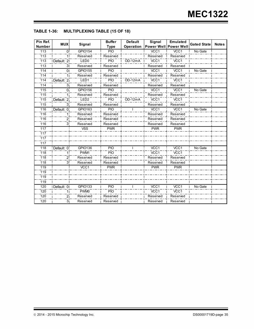
TABLE 1-36: MULTIPLEXING TABLE (15 OF 18)
Pin Ref. Number
MUX SignalBuffer Type
Default Operation
Signal Power Well
Emulated Power Well
Gated State Notes
113 0 GPIO154 PIO VCC1 VCC1 No Gate
113 1 Reserved Reserved Reserved Reserved
113 Default: 2 LED0 PIO OD-12mA VCC1 VCC1
113 3 Reserved Reserved Reserved Reserved
114 0 GPIO155 PIO VCC1 VCC1 No Gate
114 1 Reserved Reserved Reserved Reserved
114 Default: 2 LED1 PIO OD-12mA VCC1 VCC1
114 3 Reserved Reserved Reserved Reserved
115 0 GPIO156 PIO VCC1 VCC1 No Gate
115 1 Reserved Reserved Reserved Reserved
115 Default: 2 LED2 PIO OD-12mA VCC1 VCC1
115 3 Reserved Reserved Reserved Reserved
116 Default: 0 GPIO163 PIO I VCC1 VCC1 No Gate
116 1 Reserved Reserved Reserved Reserved
116 2 Reserved Reserved Reserved Reserved
116 3 Reserved Reserved Reserved Reserved
117 VSS PWR PWR PWR
117
117
117
118 Default: 0 GPIO136 PIO I VCC1 VCC1 No Gate
118 1 PWM1 PIO VCC1 VCC1
118 2 Reserved Reserved Reserved Reserved
118 3 Reserved Reserved Reserved Reserved
119 VCC1 PWR PWR PWR
119
119
119
120 Default: 0 GPIO133 PIO I VCC1 VCC1 No Gate
120 1 PWM0 PIO VCC1 VCC1
120 2 Reserved Reserved Reserved Reserved
120 3 Reserved Reserved Reserved Reserved
2014 - 2015 Microchip Technology Inc. DS00001719D-page 35

MEC1322
TABLE 1-37: MULTIPLEXING TABLE (16 OF 18)
Pin Ref. Number
MUX SignalBuffer Type
Default Operation
Signal Power Well
Emulated Power Well
Gated State Notes
121 Default: 0 GPIO034 PIO I VCC1 VCC1 No Gate
121 1 PWM2 PIO VCC1 VCC1
121 2 Reserved Reserved Reserved Reserved
121 3 TACH2PWM_OUT PIO VCC1 VCC1
122 Default: 0 GPIO135 PIO I VCC1 VCC1 No Gate
122 1 KBRST PIO VCC1 VCC1
122 2 Reserved Reserved Reserved Reserved
122 3 Reserved Reserved Reserved Reserved
123 Default: 0 GPIO044 PIO I VCC1 VCC1 No Gate
123 1 nSMI PIO VCC1 VCC1
123 2 Reserved Reserved Reserved Reserved
123 3 Reserved Reserved Reserved Reserved
124 Default: 0 GPIO066 PIO I VCC1 VCC1 No Gate
124 1 Reserved Reserved Reserved Reserved
124 2 Reserved Reserved Reserved Reserved
124 3 Reserved Reserved Reserved Reserved
125 Default: 0 GPIO025 PIO I VCC1 ON No Gate
125 1 Reserved Reserved Reserved Reserved
125 2 I2C3_DAT0 PIO VCC1 VCC1 High
125 3 Reserved Reserved Reserved Reserved
126 Default: 0 GPIO024 PIO I (PU) VCC1 VCC1 No Gate
126 1 Reserved Reserved Reserved Reserved
126 2 I2C3_CLK0 PIO VCC1 VCC1 High
126 3 Reserved Reserved Reserved Reserved
127 Default: 0 GPIO054 PIO I VCC1 VCC1 No Gate Note 10
127 1 PVT_MOSI PIO VCC1 VCC1 Note 10
127 2 Reserved Reserved Reserved Reserved
127 3 Reserved Reserved Reserved Reserved
128 Default: 0 GPIO064 PIO I VCC1 VCC1 No Gate Note 10
128 1 SHD_MOSI PIO VCC1 VCC1 Note 10
128 2 Reserved Reserved Reserved Reserved
128 3 Reserved Reserved Reserved Reserved
DS00001719D-page 36 2014 - 2015 Microchip Technology Inc.

MEC1322
TABLE 1-38: MULTIPLEXING TABLE (17 OF 18)
Pin Ref. Number
MUX SignalBuffer Type
Default Operation
Signal Power Well
Emulated Power Well
Gated State Notes
129 Default: 0 GPIO067 PIO I (PD) VCC1 ON No Gate
129 1 Reserved Reserved Reserved Reserved
129 2 Reserved Reserved Reserved Reserved
129 3 Reserved Reserved Reserved Reserved
130 Default: 0 GPIO055 PIO I (PD) VCC1 ON No Gate
130 1 Reserved Reserved Reserved Reserved
130 2 Reserved Reserved Reserved Reserved
130 3 Reserved Reserved Reserved Reserved
131 Default: 0 GPIO210 PIO I (PD) VCC1 ON No Gate
131 1 Reserved Reserved Reserved Reserved
131 2 Reserved Reserved Reserved Reserved
131 3 Reserved Reserved Reserved Reserved
132 Default: 0 GPIO211 PIO I (PD) VCC1 ON No Gate
132 1 Reserved Reserved Reserved Reserved
132 2 Reserved Reserved Reserved Reserved
132 3 Reserved Reserved Reserved Reserved
133 Default: 0 GPIO200 PIO I (PD) VCC1 ON No Gate
133 1 Reserved Reserved Reserved Reserved
133 2 Reserved Reserved Reserved Reserved
133 3 Reserved Reserved Reserved Reserved
134 Default: 0 GPIO123 PIO I (PD) VCC1 ON No Gate
134 1 Reserved Reserved Reserved Reserved
134 2 Reserved Reserved Reserved Reserved
134 3 Reserved Reserved Reserved Reserved
135 VCC1 PWR PWR PWR
135
135
135
136 Default: 0 GPIO202 PIO I (PD) VCC1 ON No Gate
136 1 Reserved Reserved Reserved Reserved
136 2 Reserved Reserved Reserved Reserved
136 3 Reserved Reserved Reserved Reserved
2014 - 2015 Microchip Technology Inc. DS00001719D-page 37

MEC1322
TABLE 1-39: MULTIPLEXING TABLE (18 OF 18)
Pin Ref. Number
MUX SignalBuffer Type
Default Operation
Signal Power Well
Emulated Power Well
Gated State Notes
137 Default: 0 GPIO201 PIO I (PD) VCC1 ON No Gate
137 1 Reserved Reserved Reserved Reserved
137 2 Reserved Reserved Reserved Reserved
137 3 Reserved Reserved Reserved Reserved
138 VSS PWR PWR PWR
138
138
138
139 Default: 0 GPIO203 PIO I (PD) VCC1 ON No Gate
139 1 Reserved Reserved Reserved Reserved
139 2 Reserved Reserved Reserved Reserved
139 3 Reserved Reserved Reserved Reserved
140 VSS PWR PWR PWR
140
140
140
141 Default: 0 GPIO204 PIO I (PD) VCC1 ON No Gate
141 1 Reserved Reserved Reserved Reserved
141 2 Reserved Reserved Reserved Reserved
141 3 Reserved Reserved Reserved Reserved
142 NC
142
142
142
143 VSS PWR PWR PWR
143
143
143
144 VSS PWR PWR PWR
144
144
144
DS00001719D-page 38 2014 - 2015 Microchip Technology Inc.

MEC1322
1.6 Notes for Tables in this Chapter
1.7 Pin States After VCC1 Power-On
Pins that default to IOD or OD in the Multiplexing Tables are open drain and come up tri-stated after VCC1 power-on.Pins that default to I are inputs and also come up tri-stated (high-z).
Table 1-40 shows pins that have specific states after VCC1 power-on.
Note 1 The LAD and SER_IRQ pins require an external weak pull-up resistor of 10k-100k ohms.Note 2 When the JTAG_RST# pin is not asserted (logic '1'), the JTAG_TDI, JTAG_TDO, JTAG_TCK, JTAG_TMS
signal functions in the JTAG interface are unconditionally routed to the interface; the Pin Control register for these pins has no effect. When the JTAG_RST# pin is asserted (logic '0'), the JTAG_TDI, JTAG_TDO, JTAG_TCK, JTAG_TMS signal functions in the JTAG interface are not routed to the interface and the Pin Control Register for these pins controls the muxing. The pin control registers can not be used to route the JTAG interface to the pins. The System Board Designer should terminate this pin in all functional states using jumpers and pull-up or pull down resistors, etc.
Note 3 An external cap must be connected as close to the CAP pin/ball as possible with a routing resistance and CAP ESR of less than 100mohms. The capacitor value is 1uF and must be ceramic with X5R or X7R dielectric. The cap pin/ball should remain on the top layer of the PCB and traced to the CAP. Avoid adding vias to other layers to minimize inductance.
Note 4 A pull-down is required on the GPIO146/PVT_CS0# pin if there is no private SPI flash device on the board.
Note 5 This I2C port supports 1Mbps (pin 88, GPIO023/I2C1_DAT0 and pin 89, GPIO022/I2C1_CLK0). For 1Mbps I2C recommended capacitance/pull-up relationships from Intel, refer to the Shark Bay platform guide, Intel ref number 486714. Refer to the PCH - SMBus 2.0/SMLink Interface Design Guidelines, Table 20-5 Bus Capacitance/Pull-Up Resistor Relationship.
Note 6 The following glitch protected pins require a pull-down on the board: pin 60, nRESET_OUT/GPIO121 and pin 85, GPIO143/RSMRST#. The nRESET_OUT pin will drive low when VCC1 comes on and stays low until the iRESET_OUT bit is cleared after VCC PWRGD asserts. The RSMRST# pin also drives low (as a GPIO push-pull output) following a VCC1 power-on until firmware deasserts it by writing the GPIO data bit to '1'. The GPIO143/RSMRST# pin operates in this manner as a GPIO; the RSMRST# function is not a true alternate function and the GPIO143 control register must not be changed from the GPIO default function.
Note 7 The BC DAT pin requires a weak pull up resistor (100 K Ohms).Note 8 The voltage on the ADC pins must not exceed 3.6 V or damage to the device will occur.Note 9 The XTAL1 pin should be left floating when using the XTAL2 pin for the single ended clock input.Note 10 MEC1322: The SPI pins are configured to their SPI function by ROM boot code as follows. Shared SPI
pins are configured to the following SPI functions: SHD_CLK, SHD_MOSI, SHD_MISO and SHD_CS0#. If the PVT_CS0# pin (pin 96) is sampled high, then the private SPI pins are configured to the following SPI functions after a successful load from flash: PVT_CLK, PVT_MOSI, PVT_MISO and PVT_CS0#; otherwise these pins are left as the GPIO function. It is recommended that user code reconfigures the shared SPI pins to the GPIO input function before releasing RSMRST#.
Note 11 The KSI[7:0] pins have the internal pull-up enabled by ROM boot code. Therefore the Buffer Type on these pins is I (PU) after the ROM boot code runs.
Note 12 The GPIO041 pin defaults to output low. This pin must be reprogrammed to the GPIO function upon power-up.
2014 - 2015 Microchip Technology Inc. DS00001719D-page 39

MEC1322
TABLE 1-40: PIN STATES AFTER VCC1 POWER-ON
P in Re fe re n ce
Nu m b e rP in Na m e P in S ta te a fte r V CC1 P ow e r-o n
21 K S O 0 0 /G P IO 0 0 0 /JTAG _ TC K P u s h -p u ll - H ig h
20 K S O 0 1 /G P IO 1 0 0 /JTAG _ TMS P u s h -p u ll - H ig h
19 K S O 0 2 /G P IO 1 0 1 /JTAG _ TD I P u s h -p u ll - H ig h
18 K S O 0 3 /G P IO 1 0 2 /JTAG _ TD O P u s h -p u ll - H ig h
17K S O 0 4 /G P IO 1 0 3 /TFD P _ D ATA/XN O
RP u s h -p u ll - H ig h
16 K S O 0 5 /G P IO 1 0 4 /TFD P _ C L K P u s h -p u ll - H ig h
13 K S O 0 6 /G P IO 0 0 1 P u s h -p u ll - H ig h
12 K S O 0 7 /G P IO 0 0 2 P u s h -p u ll - H ig h
10 K S O 0 8 /G P IO 0 0 3 P u s h -p u ll - H ig h
9 K S O 0 9 /G P IO 1 0 6 P u s h -p u ll - H ig h
8 K S O 1 0 /G P IO 0 0 4 P u s h -p u ll - H ig h
7 K S O 1 1 /G P IO 1 0 7 P u s h -p u ll - H ig h
6 K S O 1 2 /G P IO 0 0 5 P u s h -p u ll - H ig h
5 K S O 1 3 /G P IO 0 0 6 P u s h -p u ll - H ig h
113 L E D 0 /G P IO 1 5 4 O D - lo w
114 L E D 1 /G P IO 1 5 5 O D - lo w
115 L E D 2 /G P IO 1 5 6 O D - lo w
66 P S 2 _ C L K 0 /G P IO 0 4 6 IO D - lo w
61 P S 2 _ C L K 1 /G P IO 0 5 0 IO D - lo w
35 P S 2 _ C L K 2 /G P IO 0 5 1 IO D - lo w
60
n R E S E T_ O U T/G P IO 1 2 1
G litch P ro te c te d - d rive n lo w w h ile VC C 1 is ris in g .
Th e p in b e co m e s a p u s h -p u ll o u tp u t a fte r VC C 1 is u p a n d s ta b le (re q u ire s a p u ll-d o w n o n th e
b o a rd )
77
VC C 1 _ R S T# /G P IO 1 3 1
G litch P ro te c te d - d rive n lo w w h ile VC C 1 is ris in g .
Th e p in b e co m e s O D a fte r VC C 1 is u p a n d s ta b le (re q u ire s a p u ll-u p o n th e b o a rd )
85
G P IO 1 4 3 /R S MR S T#
G litch P ro te c te d - d rive n lo w w h ile VC C 1 is ris in g .
Th e p in b e co m e s a p u s h -p u ll o u tp u t a fte r VC C 1 is u p a n d s ta b le (re q u ire s a p u ll-d o w n o n th e
b o a rd )
125 G P IO 0 2 5 /I2 C 3 _ D AT0G litch P ro te c te d - d rive n lo w w h ile VC C 1 is ris in g .Th e p in b e co m e s a n in p u t (i.e ., tri-s ta te d O D typ e )
a fte r VC C 1 is u p a n d s ta b le .
DS00001719D-page 40 2014 - 2015 Microchip Technology Inc.
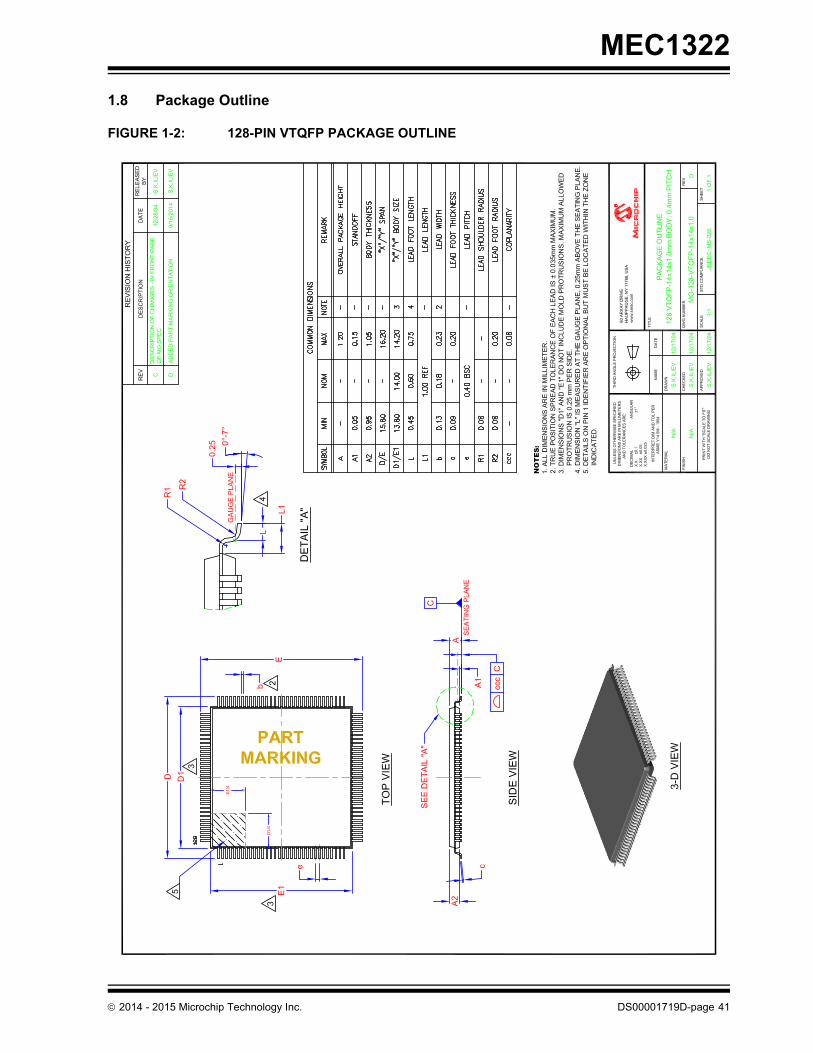
MEC1322
1.8 Package Outline
FIGURE 1-2: 128-PIN VTQFP PACKAGE OUTLINE
2014 - 2015 Microchip Technology Inc. DS00001719D-page 41

MEC1322
FIGURE 1-3: 132-PIN DQFN PACKAGE OUTLINE (1 OF 2)
DS00001719D-page 42 2014 - 2015 Microchip Technology Inc.

MEC1322
FIGURE 1-4: 132-PIN DQFN PACKAGE OUTLINE (2 OF 2)
2014 - 2015 Microchip Technology Inc. DS00001719D-page 43

MEC1322
FIGURE 1-5: 144-PIN WFBGA PACKAGE OUTLINE
DS00001719D-page 44 2014 - 2015 Microchip Technology Inc.

MEC1322
2.0 BLOCK OVERVIEW
This Chapter provides an overview of the blocks in the MEC1322.
The block diagram of the MEC1322 is shown in Figure 2-1.
Table 2-1 on page 46 lists Address Ranges for each of the blocks.
FIGURE 2-1: BLOCK DIAGRAM
ADC Ch0-4
PECI
Shared SPI
Master
PWM0
Tach 0
PWM3
LPC
RPM_PWM
Debugand Test
BC-Link
LED Control (x4)Glue Logic
nRESET_OUT, VCC1 _RST#
VREF_PECI
GPIO
VBAT Resources
PS/2 PS/2
Crystal Osc
PM1
ACPI EC (x2)
MBX
8042 KBC
Interfaces
UART
Port92
PnP CFG
Executable SRAM
VBAT RAM
VBAT Regs.
Boot ROM
RingOsc
KB Scan
On-Chip Clocking
PWM2
SMB0
Port 0
Port 1
Private SPI
Master
Clock Gen & Dist
Timer16-bit x4
Timer32-bit x2
Hibernation Timer
WDT
Tach 1
SMB1
Port 0
SMB2
Port 0
SMB3
Port 0
EC_Reg Bank
TFDP
DMA Controller
Interrupt Aggregater
RTC
EMI
PS/2 PS/2
PWM1
ADC to PWM
EC Core
Floating Point Unit
2014 - 2015 Microchip Technology Inc. DS00001719D-page 45
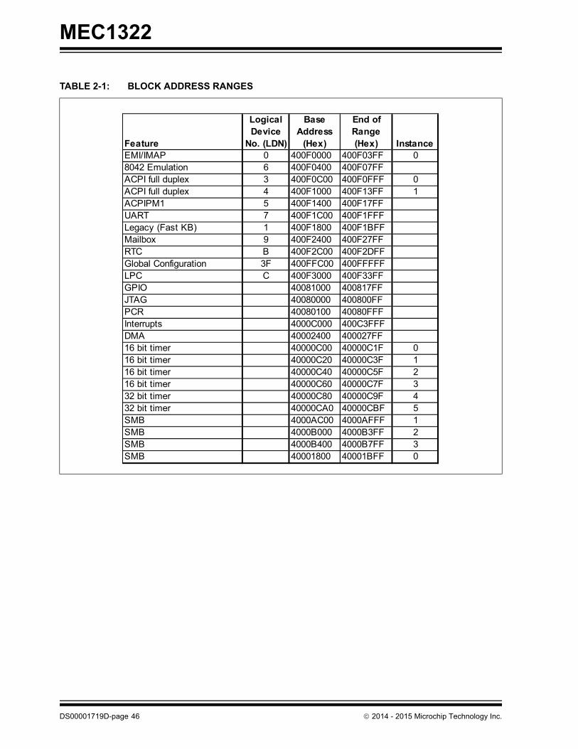
MEC1322
TABLE 2-1: BLOCK ADDRESS RANGES
Feature
Logical Device
No. (LDN)
Base Address
(Hex)
End of Range (Hex) Instance
EMI/IMAP 0 400F0000 400F03FF 08042 Emulation 6 400F0400 400F07FFACPI full duplex 3 400F0C00 400F0FFF 0ACPI full duplex 4 400F1000 400F13FF 1ACPIPM1 5 400F1400 400F17FFUART 7 400F1C00 400F1FFFLegacy (Fast KB) 1 400F1800 400F1BFFMailbox 9 400F2400 400F27FFRTC B 400F2C00 400F2DFFGlobal Configuration 3F 400FFC00 400FFFFFLPC C 400F3000 400F33FFGPIO 40081000 400817FFJTAG 40080000 400800FFPCR 40080100 40080FFFInterrupts 4000C000 400C3FFFDMA 40002400 400027FF16 bit timer 40000C00 40000C1F 016 bit timer 40000C20 40000C3F 116 bit timer 40000C40 40000C5F 216 bit timer 40000C60 40000C7F 332 bit timer 40000C80 40000C9F 432 bit timer 40000CA0 40000CBF 5SMB 4000AC00 4000AFFF 1SMB 4000B000 4000B3FF 2SMB 4000B400 4000B7FF 3SMB 40001800 40001BFF 0
DS00001719D-page 46 2014 - 2015 Microchip Technology Inc.

MEC1322
TABLE 2-1: BLOCK ADDRESS RANGES (CONTINUED)
Feature
Logical Device
No. (LDN)
Base Address
(Hex)
End of Range (Hex) Instance
64 Byte VBAT RAM 4000A800 4000ABFFVBAT Registers 4000A400 4000A7FFRPM FAN 4000A000 4000A3FFKeyScan 40009C00 40009FFFHibernation Timer 40009800 40009BFFGP-SPI 40009400 4000947F 0GP-SPI 40009480 400094FF 1PS/2 40009000 4000903F 0PS/2 40009040 4000907F 1PS/2 40009080 400090BF 2PS/2 400090C0 400090FF 3ADC 40007C00 40007C7FPWM 40005800 4000580F 0PWM 40005810 4000581F 1PWM 40005820 4000582F 2PWM 40005830 4000583F 3TACH 40006000 4000600F 0TACH 40006010 4000601F 1WDT 40000400 400007FFTFDP 40008C00 40008FFFBC-Link 4000BC00 4000BFFFPECI 40006400 400067FFB/B LED 4000B800 4000B8FF 0B/B LED 4000B900 4000B9FF 1B/B LED 4000BA00 4000BAFF 2B/B LED 4000BB00 4000BBFF 3EC_REG_BANK 4000FC00 4000FC1BData Space SRAM 00118000 0011FFFFCode Space SRAM 00100000 00117FFFROM 00000000 00007FFF
2014 - 2015 Microchip Technology Inc. DS00001719D-page 47
MEC1322
3.0 POWER, CLOCKS, AND RESETS
3.1 Introduction
The Power, Clocks, and Resets (PCR) chapter identifies all the power supplies, clock sources, and reset inputs to thechip and defines all the derived power, clock, and reset signals. In addition, this section identifies Power, Clock, andReset events that may be used to generate an interrupt event, as well as, the Chip Power Management Features.
3.2 References
No references have been cited for this chapter.
3.3 Interrupts
The Power, Clocks, and Resets logic generates no events
3.4 Power
3.4.1 POWER SOURCES
Table 3-1 lists the power supplies from which the MEC1322 draws current. These current values are defined in Section37.4, "Power Consumption," on page 395.
Note 3-1 Note on Battery Replacement: Microchip recommends removing all power sources to the devicedefined in Table 3-1, "Power Source Definitions" and all external voltage references defined inTable 3-2, "Voltage Reference Definitions" before removing and replacing the battery. In addition,upon removing the battery, ground the battery pin before replacing the battery.
APPLICATION NOTE: Battery Circuit Requirement:
• VCC0 must always be present if VCC1 is present.
TABLE 3-1: POWER SOURCE DEFINITIONS
Power WellNominal Voltage
Description Source
VCC1 3.3V Main Battery Pack Supply Power Well. This is the “Always-on” supply.
Pin Interface
VBAT(VCC0)
(Note 3-1)
3.0V System Battery Back-up Power Well. This is the “coin-cell” battery.
Pin Interface
Note: The Minimum rise/fall time requirement on VCC1 is 200us.
Note: The Minimum rise time requirement on VBAT is 100us.
DS00001719D-page 48 2014 - 2015 Microchip Technology Inc.

MEC1322
The following circuit is recommended to fulfill this requirement:
FIGURE 3-1: RECOMMENDED BATTERY CIRCUIT
3.4.2 VOLTAGE REFERENCES
Table 3-2 lists the External Voltage References to which the MEC1322 provides high impedance interfaces.
Note 3-2 The VREF_PECI does not have a power good signal associated with it. See VREF Buffer typedefinition in Table 37-4, “DC Electrical Characteristics,” on page 391.
3.4.3 POWER GOOD SIGNALS
The power good timing and thresholds are defined in the Section 38.1, "Voltage Thresholds and Power Good Timing,"on page 397.
TABLE 3-2: VOLTAGE REFERENCE DEFINITIONS
Power WellNominal Input
VoltageScaling Ratio
Nominal Monitored
VoltageDescription Source
VREF_PECI(Note 3-2)
Variable n/a Variable Processor Voltage External Voltage Reference
Used to scale Processor Interface signals
Pin Interface
TABLE 3-3: POWER GOOD SIGNAL DEFINITIONS
Power Good Signal
Description Source
VCC1GD VCC1GD is an internal power good signal used to indicate when the VCC1 rail is on and stable.
VCC1GD is asserted following a delay after the VCC1 power well exceeds its preset voltage threshold. VCC1GD is de-assertedas soon as this voltage drops below this thresh-old.
PWRGD PWRGD is used to indicate when the main power rail voltage is on and stable.
VCC_PWRGD Input pin
VCC0 to EC
To EC asVCC1
3.0V nom Coin Cell
“RTC” Rail (PCH, System)
+(Schottky
Diode)
(Schottky Diode)
3.3V nom, from AC Source or Battery Pack
( )Possible
Current Limiter(1K typ.)
3.3V max with VCC1 = 0V,
3.6V max with VCC1 = VBAT
2014 - 2015 Microchip Technology Inc. DS00001719D-page 49

MEC1322
3.4.4 SYSTEM POWER SEQUENCING
The following table defines the behavior of the Power Sources in each of the defined ACPI power states.
Note 3-3 VCC1 power supply is always on while the battery pack or ac power is applied to the system.
Note 3-4 This device requires that the VBAT power is on when the VCC1 power supply is on. External circuitry,a diode isolation circuit, is implemented on the motherboard to extend the battery life. This externalcircuitry ensures the VBAT pin will derive power from the VCC1 power well when it is on. Therefore,the VBAT supply will never appear to be off when the VCC1 rail is on. See APPLICATION NOTE: onpage 48.
3.5 Clocks
The following section defines the MEC1322 clocks that are generated or referenced.
TABLE 3-4: TYPICAL POWER SUPPLIES VS. ACPI POWER STATES
SupplyName
ACPI Power State
DescriptionS0(FULL ON)
S1(POS)
S3(STR)
S4(STD)
S5(Soft Off)
G3(MECH Off)
VCC1 ON ON ON ON ON OFF MEC1322 “Always-on” Supply. (Note 3-3)
VBAT (VCC0) ON ON ON ON(Note 3-4)
ON (Note 3-4)
ON(Note 3-4)
MEC1322 Battery Back-up Supply
TABLE 3-5: CLOCK DEFINITIONS
Clock Name Frequency Description Source
SUSCLK 32.768 KHz 32.768 kHz Suspend Well Clock Source is a single-ended input that is an accurate 32.768KHz clock. (Note 3-5)
Pin Interface (XTAL2)
32.768 kHz Crystal Oscillator
32.768 KHz A 32.768 KHz parallel resonant crys-tal connected between the XTAL1 and XTAL2 pins.
Pin Interface (XTAL1 and XTAL2)
48 MHz Ring Oscillator
48MHz The 48 MHz Ring Oscillator is a high-accuracy, low power, low start-up latency 48 MHz Ring Oscillator.
Enabled by VCC1 Power (Note 3-6). May be stopped by Chip Power Man-agement Features.
24MHz_Clk 24 MHz Derived clock for UART 48 MHz Ring Oscillator
16MHz_Clk 16MHz Derived clock for SMBus Controller 48 MHz Ring Oscillator
1.8432MHz_Clk 1.843 MHz Derived clock for UART 48 MHz Ring Oscillator
100kHz_Clk 100 kHz Derived for several blocks in the EC Subsystem, including, but not limited to, PWM, TACH.
48 MHz Ring Oscillator
32KHz_Clk 32.768 KHz Internal 32kHz clock domain Pin Interface:XTAL2: 32KHz Crystal input/ single-ended clock source input pin.XTAL1: 32KHz Crystal output
The XOSEL bit configures the source of this clock domain as either a sin-gle-ended 32.768 KHz clock input (SUSCLK) or the 32.768 kHz Crystal Oscillator (Note 3-7). If neither of these is available, this clock domain is derived from the 48 MHz Ring Oscillator.
DS00001719D-page 50 2014 - 2015 Microchip Technology Inc.

MEC1322
Note 3-5 The chipset will not produce a valid 32KHz clock until about 5 ms (PCH) or 110 ms (ICH) after thedeassertion of RSMRST#. See chipset specification for the actual timing.
Note 3-6 The 48 MHz Ring Oscillator is reset by VCC1GD.
Note 3-7 The Clock Enable Register contains the XOSEL bit and the 32K_EN bit (see Section 4.7.2, "ClockEnable Register," on page 73). The 32.768 KHz Oscillator provides a stable timebase for the 48 MHzRing Oscillator as well as the clock source for the 32KHz Clock Domain. After VBAT POR there is a500ms max time for the 48 MHz Ring Oscillator to become accurate.
3.5.1 32KHZ CLOCK SWITCHING
The 32kHz clock switching logic switches the clock source of the 32kHz clock domain to be either the single-ended32.768 KHz clock input or the 32.768 kHz Crystal Oscillator. If neither of these is available, this clock domain is derivedfrom the 48 MHz Ring Oscillator.
Following a VBAT_POR, the XOSEL bit and the 32K_EN bit in the Clock Enable Register are programmed to configurethe source of this clock domain.
If the single-ended 32.768 KHz clock input is configured as the source of the 32kHz clock domain, then following aVCC1_RESET, the time for this clock domain to become accurate at 32.768kHz after the SUSCLK input goes active is100us (max).
If the 32.768 kHz Crystal Oscillator is configured as the source of the 32kHz clock domain, then following a VCC1_RE-SET, there is 100us (max) delay time for this clock domain to become accurate at 32.768kHz.
3.5.2 CLOCK DOMAINS VS. ACPI POWER STATES
Table 3-6, "Typical MEC1322 Clocks vs. ACPI Power States" shows the relationship between ACPI power states andMEC1322 clock domains:
TABLE 3-6: TYPICAL MEC1322 CLOCKS VS. ACPI POWER STATES
ClockName
ACPI Power State
DescriptionS0(FULLON)
S1(POS)
S3(STR)
S4(STD)
S5(SoftOff)
G3(MECH
Off)
SUSCLK ON ON ON ON ON OFF This clock is the system suspend clock source. (Note 3-5).
32.768 kHz Crystal Oscillator
ON ON ON ON ON ON This clock is generated from a 32.768 KHz paral-lel resonant crystal con-nected between the XTAL1 and XTAL2 pins.
32KHz_Clk ON ON ON ON ON ON/ OFF This clock domain is gen-erated from the 32KHz clock input (SUSCLK) when available or the crystal oscillator pins. Otherwise it is generated internally from the 48 MHz Ring Oscillator.
2014 - 2015 Microchip Technology Inc. DS00001719D-page 51

MEC1322
3.6 Resets
48 MHz Ring Oscilla-tor
ON ON ON ON ON OFF This clock is powered by the MEC1322 suspend supply (VCC1) but may start and stop as described in Section 3.7, "Chip Power Manage-ment Features," on page 54 (see also Note 3-3).
TABLE 3-7: DEFINITION OF RESET SIGNALS
Reset Description Source
VBAT_POR Internal VBAT Reset signal. This signal is used to reset VBAT powered registers.
VBAT_POR is a pulse that is asserted at the ris-ing edge of VCC1GD if the VBAT voltage is below a nominal 1.25V. VBAT_POR is also asserted as a level if, while VCC1GD is not asserted (‘0’), the coin cell is replaced with a new cell that delivers at least a nominal 1.25V. In this latter case VBAT_POR is de-asserted when VCC1GD is asserted. No action is taken if the coin cell is replaced, or if the VBAT voltage falls below 1.25 V nominal, while VCC1GD is asserted.
VCC1_RESET Internal VCC1 Reset signal. This signal is used to reset VCC1 powered registers.
VCC1_RESET is asserted when VCC1GD is low and is deasserted when VCC1GD is high. The VCC1_RST# pin asserted as input will also cause a VCC1_RESET. A WDT_RESET event will also cause a VCC1_RESET assertion.
PCI RESET# System reset signal connected to the LPC LRESET# pin.
Pin Interface, LRESET# pin. See Note 3-8.
nSIO_RESET Performs a reset when VCC is turned off or when the system host resets the LPC Interface.
nSIO_RESET is a signal that is asserted if VCC1GD is low, PWRGD is low, or PCI RESET# is asserted low and may be deasserted when these three signals are all high. The iRE-SET_OUT bit controls the deassertion of nSIO_RESET. See Note 3-8.A WDT_RESET event will also cause an nSIO_RESET assertion.
TABLE 3-6: TYPICAL MEC1322 CLOCKS VS. ACPI POWER STATES (CONTINUED)
ClockName
ACPI Power State
DescriptionS0(FULLON)
S1(POS)
S3(STR)
S4(STD)
S5(SoftOff)
G3(MECH
Off)
DS00001719D-page 52 2014 - 2015 Microchip Technology Inc.

MEC1322
Note 3-8 If the LRESET# pin is assigned to the GPIO function rather than LRESET#, the internal LRESET#signal is gated low, and therefore the nRESET_OUT function will not operate properly.
3.6.1 INTEGRATED VCC1 POWER ON RESET (VCC1_RST#)
The VCC1_RST# pin is used to control the power up sequence for external devices. The VCC1_RST# timing is shownin Section 38.1.1, "VCC1_RST# Timing," on page 397.
The following summarizes the operation of the VCC1_RST# signal.
• The VCC1_RST# pin is both a reset input and an output to the system.
• The VCC1_RST# output provides a POR reset during power up transition
• The VCC1_RST# output has Output Pin Glitch Protection
• The VCC1_RST# output stretches an external driven reset by 1ms (typ).
• The VCC1_RST# input detects an externally driven reset and places the MEC1322 into a VCC1 POR state.
The VCC1_RST# is an open drain pin. An external pull-up is required for the VCC1_RST# signal to be high.
The following sequence illustrates the interaction between the internally and externally driven assertion of VCC1_RST#:
1. The Integrated VCC1 Power On Reset Generator insures VCC1_RST# is driven low during a VCC1 POR fromVCC1 = 1V to 2.4V (typ) without glitches.
2. The VCC1_RST# pin is driven low during the POR transition until VCC1 > 2.4V (typ) and then the VCC1_RST#pin remains low afterwards for 1ms (typ) delay window. The VCC1_RST# input is not examined during the 1ms(typ) delay window; therefore, the system input and/or the external pin termination may be modified (i.e. drive itlow, let it float, etc.)
- The VCC1_RST# input is not examined during the POR transition while VCC1 < 2.4V (typ); therefore, the system input to the VCC1_RST# pin may modify the output termination (i.e. drive it low, let it float, etc.)
3. The VCC1_RST# pin is driven low during the 1ms (typ) delay window. The MEC1322 is in the VCC1_POR stateduring this time.
4. After the 1ms (typ) window, the VCC1_RST# pin open drain output from the MEC1322 is not driven/released.The strap option pins are sampled at this time.
5. The MEC1322 will remain in the VCC1 POR for 2.65us (min) after the VCC1_RST# pin is released TheVCC1_RST# input pin is ignored during this time.
6. The VCC1_RST# pin input is sampled at 2.65us (min) after the VCC1_RST# pin is released.
- If the VCC1_RST# pin is high when sampled, then the EC starts executing.
- If the VCC1_RST# pin is low when sampled, the pin is being driven externally (i.e., the system is forcing a reset):
- The VCC1_RST# pin is driven low for 1ms (typ), then sampled at 2.65us (min) after the VCC1_RST# pin is released (see step 3).
WDT_RESET Internal WDT Reset signal. This signal resets VCC1 powered registers with the exception of the WDT Event Count register. Note that the glitch protect circuits do not activate on a WDT reset. WDT_RESETdoes not reset VBAT registers or logic.
A WDT_RESET is asserted by a WDT Event.
Note: This event is indicated by the WDTbit in the Power-Fail and Reset Sta-tus Register
EC_PROC_ RESET
Internal reset signal to reset the processor in the EC Subsystem.
An EC_PROC_ RESET is a stretched version of the VCC1_RESET. This reset asserts at the same time that VCC1_RESET asserts and is held asserted for 1ms after the VCC1_RESET deasserts.
Note: The external pull-up on the VCC1_RST# pin must be chosen to meet the timing in Table 38-2,“VCC1_RST# Rise Time,” on page 397.
TABLE 3-7: DEFINITION OF RESET SIGNALS (CONTINUED)
Reset Description Source
2014 - 2015 Microchip Technology Inc. DS00001719D-page 53

MEC1322
Note 1: The minimum low pulse provided to initiate reset = 20ns.
2: There is no glitch protection or noise filtering (i.e. a vary narrow noise pulse cause a reset).
3.7 Chip Power Management Features
This device is designed to always operate in its lowest power state during normal operation. In addition, this deviceoffers additional programmable options to put individual logical blocks to sleep as defined in Section 3.7.1, "Block LowPower Modes," on page 54.
3.7.1 BLOCK LOW POWER MODES
All power related control signals are generated and monitored centrally in the chip’s Power, Clocks, and Resets (PCR)block. The power manager of the PCR block uses a sleep interface to communicate with all the blocks. The sleep inter-face consists of three signals:
• sleep_en (request to sleep the block) is generated by the PCR block. A group of sleep_en signals are gener-ated for every clock segment. Each group consists of a sleep_en signal for every block in that clock segment.
• clk_req (request clock on) is generated by every block. They are grouped by blocks on the same clock segment. The PCR monitors these signals to see when it can gate off clocks.
• reset_en (reset on sleep) bits determine if the block (including registers) will be reset when it enters sleep mode.
A block can always drive clk_req low synchronously, but it MUST drive it high asynchronously since its internal clocksare gated and it has to assume that the clock input itself is gated. Therefore the block can only drive clk_req high as aresult of a register access or some other input signal.
The following table defines a block’s power management protocol:
A wake event clears all sleep enable bits momentarily, and then returns the sleep enable bits back to their original state.The block that needs to respond to the wake event will do so. See Section 15.8.1, "WAKE Generation," on page 194.
The Sleep Enable, Clock Required and Reset Enable registers are defined in Section 3.8, "EC-Only Registers," onpage 55.
Power State sleep_en clk_req Description
Normal operation Low Low Block is idle and NOT requesting clocks. The block gates its own internal clock.
Normal operation Low High Block is NOT idle and requests clocks.
Request sleep Rising Edge Low Block is IDLE and enters sleep mode immediately. The block gates its own internal clock. The block cannot request clocks again until sleep_en goes low.
Request sleep Rising Edge High then Low
Block is not IDLE and will stop requesting clocks and enter sleep when it finishes what it is doing. This delay is block specific, but should be less than 1 ms. The block gates its own internal clock. After driving clk_req low, the block cannot request clocks again until sleep_en goes low.
Register Access X High Register access to a block is always available regardless of sleep_en. Therefore the block ungates its internal clock and drives clk_req high during the access. The block will regate its internal clock and drive clk_req low when the access is done.
DS00001719D-page 54 2014 - 2015 Microchip Technology Inc.

MEC1322
3.8 EC-Only Registers
Note 3-9 The Base Address indicates where the first register can be accessed in a particular address spacefor a block instance.
3.9 Sleep Enable and Clock Required Registers
The following are the Sleep Enable and Clock Required registers for the MEC1322.
3.9.1 CHIP SLEEP ENABLE REGISTER (CHIP_SLP_EN)
TABLE 3-8: EC-ONLY REGISTER BASE ADDRESS TABLE
Block InstanceInstance Number
Host Address Space Base Address (Note 3-9)
PCR 0 EC 32-bit internal address space
4008_0100h
TABLE 3-9: POWER, CLOCKS AND RESET VCC1-POWERED REGISTERS SUMMARY
Offset Register Name
00h Chip Sleep Enable Register (CHIP_SLP_EN)
04h Chip Clock Required Status Registers (CHIP_CLK_REQ_STS)
08h EC Sleep Enable Register (EC_SLP_EN)
0Ch EC Clock Required Status Registers (EC_CLK_REQ_STS)
10h Host Sleep Enable Register (HOST_SLP_EN)
14h Host Clock Required Status Registers (HOST_CLK_REQ)
18h System Sleep Control Register (SYS_SLP_CNTRL)
20h Processor Clock Control Register (PROC_CLK_CNTRL)
24h EC Sleep Enable 2 Register (EC_SLP_EN2)
28h EC Clock Required 2 Status Register (EC_CLK_REQ2_STS)
2Ch Slow Clock Control Register (SLOW_CLK_CNTRL)
30h Oscillator ID Register (CHIP_OSC_ID)
34h PCR chip sub-system power reset status (CHIP_PWR_RST_STS)
38h Chip Reset Enable Register (CHIP_RST_EN)
3Ch Host Reset Enable Register (HOST_RST_EN)
40h EC Reset Enable Register (EC_RST_EN)
44h EC Reset Enable 2 Register (EC_RST_EN2)
48h Power Reset Control (PWR_RST_CTRL) Register
Note: All register addresses are naturally aligned on 32-bit boundaries. Offsets for registers that are smaller than32 bits are reserved and must not be used for any other purpose.
Offset 00h
Bits Description Type DefaultReset Event
31:2 RESERVED RES
1 MCHP Reserved (Note 3-10) R/W 0h VCC1_RESET
0 MCHP Reserved (Note 3-10) R/W 0h VCC1_RESET
2014 - 2015 Microchip Technology Inc. DS00001719D-page 55

MEC1322
Note 3-10 MCHP Reserved bits in the sleep_en registers must be written to 1 in order for the chip to be putinto sleep mode.
3.9.2 CHIP CLOCK REQUIRED STATUS REGISTERS (CHIP_CLK_REQ_STS)
3.9.3 EC SLEEP ENABLE REGISTER (EC_SLP_EN)
Offset 04h
Bits Description Type DefaultReset Event
31:2 RESERVED RES
1 MCHP Reserved R 0h VCC1_RESET
0 MCHP Reserved R - VCC1_RESET
Offset 08h
Bits Description Type DefaultReset Event
31 TIMER16_1 Sleep Enable
0: block is free to use clocks as necessary.1: block is commanded to sleep at next available moment.See Note 3-11 on page 57.
R/W 0h VCC1_RESET
30 TIMER16_0 Sleep Enable
0: block is free to use clocks as necessary.1: block is commanded to sleep at next available moment.See Note 3-11 on page 57.
R/W 0h VCC1_RESET
29 EC_REG_BANK Sleep Enable
0: block is free to use clocks as necessary.1: block is commanded to sleep at next available moment.
R/W 0h VCC1_RESET
28:23 RESERVED RES
22 PWM3 Sleep Enable
0: block is free to use clocks as necessary.1: block is commanded to sleep at next available moment.
R/W 0h VCC1_RESET
21 PWM2 Sleep Enable
0: block is free to use clocks as necessary.1: block is commanded to sleep at next available moment.
R/W 0h VCC1_RESET
20 PWM1 Sleep Enable
0: block is free to use clocks as necessary.1: block is commanded to sleep at next available moment.
R/W 0h VCC1_RESET
19:12 RESERVED RES
11 TACH1 Sleep Enable
0: block is free to use clocks as necessary.1: block is commanded to sleep at next available moment.
R/W 0h VCC1_RESET
10 SMB0 Sleep Enable
0: block is free to use clocks as necessary.1: block is commanded to sleep at next available moment.
R/W 0h VCC1_RESET
9 WDT Sleep Enable
0: block is free to use clocks as necessary.1: block is commanded to sleep at next available moment.
R/W 0h VCC1_RESET
DS00001719D-page 56 2014 - 2015 Microchip Technology Inc.

MEC1322
Note 3-11 The basic timers in this device have an auto-reload mode. When this mode is selected, the block'sclk_req equation is always asserted, which will prevent the device from gating its clock tree and goingto sleep. When the firmware intends to put the device to sleep, none of the timers should be in auto-reload mode. Alternatively, use the timer's HALT function inside the control register to stop the timerin auto-reload mode so it can go to sleep.
3.9.4 EC CLOCK REQUIRED STATUS REGISTERS (EC_CLK_REQ_STS)
8 PROCESSOR Sleep Enable
0: block is free to use clocks as necessary.1: block is commanded to sleep at next available moment.
R/W 0h VCC1_RESET
7 TFDP Sleep Enable
0: block is free to use clocks as necessary.1: block is commanded to sleep at next available moment.
R/W 0h VCC1_RESET
6 DMA Sleep Enable
0: block is free to use clocks as necessary.1: block is commanded to sleep at next available moment.
R/W 0h VCC1_RESET
5 PMC Sleep Enable
0: block is free to use clocks as necessary.1: block is commanded to sleep at next available moment.
R/W 0h VCC1_RESET
4 PWM0 Sleep Enable
0: block is free to use clocks as necessary.1: block is commanded to sleep at next available moment.
R/W 0h VCC1_RESET
3 RESERVED RES
2 TACH0 Sleep Enable
0: block is free to use clocks as necessary.1: block is commanded to sleep at next available moment.
R/W 0h VCC1_RESET
1 PECI Sleep Enable
0: block is free to use clocks as necessary.1: block is commanded to sleep at next available moment.
R/W 0h VCC1_RESET
0 INT Sleep Enable
0: block is free to use clocks as necessary.1: block is commanded to sleep at next available moment.
R/W 0h VCC1_RESET
Offset 0Ch
Bits Description Type DefaultReset Event
31 TIMER16_1 Clock Required
0: block does NOT need clocks.1: block requires clocks.
R 0h VCC1_RESET
30 TIMER16_0 Clock Required
0: block does NOT need clocks.1: block requires clocks.
R 0h VCC1_RESET
29 EC_REG_BANK Clock Required
0: block does NOT need clocks.1: block requires clocks.
R 0h VCC1_RESET
28:23 RESERVED RES
Offset 08h
Bits Description Type DefaultReset Event
2014 - 2015 Microchip Technology Inc. DS00001719D-page 57

MEC1322
22 PWM3 Clock Required
0: block does NOT need clocks.1: block requires clocks.
R 0h VCC1_RESET
21 PWM2 Clock Required
0: block does NOT need clocks.1: block requires clocks.
R 0h VCC1_RESET
20 PWM1 Clock Required
0: block does NOT need clocks.1: block requires clocks.
R 0h VCC1_RESET
19:12 RESERVED RES
11 TACH1 Clock Required
0: block does NOT need clocks.1: block requires clocks.
R 0h VCC1_RESET
10 SMB0 Clock Required
0: block does NOT need clocks.1: block requires clocks.
R 0h VCC1_RESET
9 WDT Clock Required
0: block does NOT need clocks.1: block requires clocks.
R 0h VCC1_RESET
8 PROCESSOR Clock Required
0: block does NOT need clocks.1: block requires clocks.
R 1h VCC1_RESET
7 TFDP Clock Required
0: block does NOT need clocks.1: block requires clocks.
R 0h VCC1_RESET
6 DMA Clock Required
0: block does NOT need clocks.1: block requires clocks.
R 0h VCC1_RESET
5 PMC Clock Required
0: block does NOT need clocks.1: block requires clocks.
R 0h VCC1_RESET
4 PWM0 Clock Required
0: block does NOT need clocks.1: block requires clocks.
R 0h VCC1_RESET
3 RESERVED RES
2 TACH0 Clock Required
0: block does NOT need clocks.1: block requires clocks.
R 0h VCC1_RESET
1 PECI Clock Required
0: block does NOT need clocks.1: block requires clocks.
R 0h VCC1_RESET
0 INT Clock Required
0: block does NOT need clocks.1: block requires clocks.
R 0h VCC1_RESET
Offset 0Ch
Bits Description Type DefaultReset Event
DS00001719D-page 58 2014 - 2015 Microchip Technology Inc.

MEC1322
3.9.5 HOST SLEEP ENABLE REGISTER (HOST_SLP_EN)
3.9.6 HOST CLOCK REQUIRED STATUS REGISTERS (HOST_CLK_REQ)
Offset 10h
Bits Description Type DefaultReset Event
31:19 RESERVED RES
18 RTC Sleep Enable
0: block is free to use clocks as necessary.1: block is commanded to sleep at next available moment.
R/W 0h VCC1_RESET
17 RESERVED RES
16 8042EM Sleep Enable
0: block is free to use clocks as necessary.1: block is commanded to sleep at next available moment.
R/W 0h VCC1_RESET
15 ACPI PM1 Sleep Enable
0: block is free to use clocks as necessary.1: block is commanded to sleep at next available moment.
R/W 0h VCC1_RESET
14 ACPI EC 1 Sleep Enable
0: block is free to use clocks as necessary.1: block is commanded to sleep at next available moment.
R/W 0h VCC1_RESET
13 ACPI EC 0 Sleep Enable
0: block is free to use clocks as necessary.1: block is commanded to sleep at next available moment.
R/W 0h VCC1_RESET
12 GLBL_CFG
0: block is free to use clocks as necessary.1: block is commanded to sleep at next available moment.
R/W 0h VCC1_RESET
11:2 RESERVED RES
1 UART 0 Sleep Enable
0: block is free to use clocks as necessary.1: block is commanded to sleep at next available moment.
R/W 0h VCC1_RESET
0 LPC Sleep Enable
0: block is free to use clocks as necessary.1: block is commanded to sleep at next available moment.
R/W 0h VCC1_RESET
Offset 14h
Bits Description Type DefaultReset Event
31:19 RESERVED RES
18 RTC Clock Required
0: block does NOT need clocks.1: block requires clocks.
R 0h VCC1_RESET
17 RESERVED RES
16 8042EM Clock Required
0: block does NOT need clocks.1: block requires clocks.
R 0h VCC1_RESET
15 ACPI PM1 Clock Required
0: block does NOT need clocks.1: block requires clocks.
R 0h VCC1_RESET
2014 - 2015 Microchip Technology Inc. DS00001719D-page 59

MEC1322
3.9.7 SYSTEM SLEEP CONTROL REGISTER (SYS_SLP_CNTRL)
The System Sleep States shown in Table 3-10 and determined by the bits in this register, are only entered if all blocksare sleeping; that is, if the sleep enable bits are set for all blocks and no clocks are required.
14 ACPI EC 1 Clock Required
0: block does NOT need clocks.1: block requires clocks.
R 0h VCC1_RESET
13 ACPI EC 0 Clock Required
0: block does NOT need clocks.1: block requires clocks.
R 0h VCC1_RESET
12 GLBL_CFG Clock Required
0: block does NOT need clocks.1: block requires clocks.
R - VCC1_RESET
11:2 RESERVED RES
1 UART 0 Clock Required
0: block does NOT need clocks.1: block requires clocks.
R - VCC1_RESET
0 LPC Clock Required
0: block does NOT need clocks.1: block requires clocks.
R - VCC1_RESET
Offset 18h
Bits Description Type DefaultReset Event
31:3 RESERVED RES
2 Core regulator standby
0: keep regulator fully operational when sleeping.1: standby the regulator when sleeping. Allows enough power for chip static operation for memory retention.
R/W 0h VCC1_RESET
1 Ring oscillator output gate
0: keep ROSC ungated when sleeping.1: gate the ROSC output when sleeping.
R/W 0h VCC1_RESET
0 Ring oscillator power down
0: keep ROSC operating when sleeping.1: disable ROSC when sleeping. Clocks will start on wakeup, but there is a clock lock latency penalty.
R/W 0h VCC1_RESET
Offset 14h
Bits Description Type DefaultReset Event
DS00001719D-page 60 2014 - 2015 Microchip Technology Inc.

MEC1322
Note 3-12 This is the latency following a wake event until the 48 MHz Ring Oscillator is locked and clocking thesystem.
3.9.8 PROCESSOR CLOCK CONTROL REGISTER (PROC_CLK_CNTRL)
3.9.9 EC SLEEP ENABLE 2 REGISTER (EC_SLP_EN2)
TABLE 3-10: SYSTEM SLEEP CONTROL BIT ENCODING
D2 D1 D0Wake Latency
(TYP)Description
0 0 0 0 The Core regulator and the Ring Oscillator remain powered and run-ning during sleep cycles (SYSTEM HEAVY SLEEP 1) (DEFAULT)
0 1 0 0 The Core regulator remains powered and the Ring oscillator is running but gated during sleep cycles (SYSTEM HEAVY SLEEP 2)
0 X 1 200us(Note 3-12)
The Core regulator remains powered and the Ring oscillator is powered down during sleep cycles (SYSTEM HEAVY SLEEP 3)
1 X 1 1ms The Core regulator is suspended and the Ring oscillator is powered down during sleep cycles. (SYSTEM DEEPEST SLEEP)
Offset 20h
Bits Description Type DefaultReset Event
31:8 RESERVED RES
7:0 Processor Clock Divide Value
1: divide 48 MHz Ring Oscillator by 1.4: divide 48 MHz Ring Oscillator by 4.16: divide 48 MHz Ring Oscillator by 16.48: divide 48 MHz Ring Oscillator by 48.No other values are supported.
R/W 4h VCC1_RESET
Offset 24h
Bits Description Type DefaultReset Event
31:29 RESERVED RES
28 MCHP Reserved (Note 3-10) R/W 0h VCC1_RESET
27 MCHP Reserved (Note 3-10) R/W 0h VCC1_RESET
26 MCHP Reserved (Note 3-10) R/W 0h VCC1_RESET
25 LED3 Sleep Enable
0: block is free to use clocks as necessary.1: block is commanded to sleep at next available moment.
R/W 0h VCC1_RESET
24 TIMER32_1 Sleep Enable
0: block is free to use clocks as necessary.1: block is commanded to sleep at next available moment.See Note 3-11 on page 57.
R/W 0h VCC1_RESET
23 TIMER32_0 Sleep Enable
0: block is free to use clocks as necessary.1: block is commanded to sleep at next available moment.See Note 3-11 on page 57.
R/W 0h VCC1_RESET
2014 - 2015 Microchip Technology Inc. DS00001719D-page 61

MEC1322
22 TIMER16_3 Sleep Enable
0: block is free to use clocks as necessary.1: block is commanded to sleep at next available moment.See Note 3-11 on page 57.
R/W 0h VCC1_RESET
21 TIMER16_2_Sleep Enable
0: block is free to use clocks as necessary.1: block is commanded to sleep at next available moment.See Note 3-11 on page 57.
R/W 0h VCC1_RESET
20 SPI1 Sleep Enable
0: block is free to use clocks as necessary.1: block is commanded to sleep at next available moment.
R/W 0h VCC1_RESET
19 BCM Sleep Enable
0: block is free to use clocks as necessary.1: block is commanded to sleep at next available moment.
R/W 0h VCC1_RESET
18 LED2 Sleep Enable
0: block is free to use clocks as necessary.1: block is commanded to sleep at next available moment.
R/W 0h VCC1_RESET
17 LED1 Sleep Enable
0: block is free to use clocks as necessary.1: block is commanded to sleep at next available moment.
R/W 0h VCC1_RESET
16 LED0 Sleep Enable
0: block is free to use clocks as necessary.1: block is commanded to sleep at next available moment.
R/W 0h VCC1_RESET
15 SMB3 Sleep Enable
0: block is free to use clocks as necessary.1: block is commanded to sleep at next available moment.
R/W 0h VCC1_RESET
14 SMB2 Sleep Enable
0: block is free to use clocks as necessary.1: block is commanded to sleep at next available moment.
R/W 0h VCC1_RESET
13 SMB1 Sleep Enable
0: block is free to use clocks as necessary.1: block is commanded to sleep at next available moment.
R/W 0h VCC1_RESET
12 RPM-PWM Sleep Enable
0: block is free to use clocks as necessary.1: block is commanded to sleep at next available moment.
R/W 0h VCC1_RESET
11 KEYSCAN Sleep Enable
0: block is free to use clocks as necessary.1: block is commanded to sleep at next available moment.
R/W 0h VCC1_RESET
10 HTIMER Sleep Enable
0: block is free to use clocks as necessary.1: block is commanded to sleep at next available moment.
R/W 0h VCC1_RESET
9 SPI0 Sleep Enable
0: block is free to use clocks as necessary.1: block is commanded to sleep at next available moment.
R/W 0h VCC1_RESET
8 PS2_3 Sleep Enable
0: block is free to use clocks as necessary.1: block is commanded to sleep at next available moment.See Note 3-14.
R/W 0h VCC1_RESET
Offset 24h
Bits Description Type DefaultReset Event
DS00001719D-page 62 2014 - 2015 Microchip Technology Inc.

MEC1322
Note 3-13 The ADC VREF must be powered down in order to get the lowest deep sleep current. The ADCVREF Power down bit, ADC_VREF_PD_REF is in the EC Subsystem Registers ADC VREF PD onpage 381.
Note 3-14 The PS2 block will only sleep while the PS2 is disabled or in Rx mode with no traffic on the bus.
3.9.10 EC CLOCK REQUIRED 2 STATUS REGISTER (EC_CLK_REQ2_STS)
7 PS2_2 Sleep Enable
0: block is free to use clocks as necessary.1: block is commanded to sleep at next available moment.See Note 3-14.
R/W 0h VCC1_RESET
6 PS2_1 Sleep Enable
0: block is free to use clocks as necessary.1: block is commanded to sleep at next available moment.See Note 3-14.
R/W 0h VCC1_RESET
5 PS2_0 Sleep Enable
0: block is free to use clocks as necessary.1: block is commanded to sleep at next available moment.See Note 3-14.
R/W 0h VCC1_RESET
4 MCHP Reserved (Note 3-10)
R/W 0h VCC1_RESET
3 ADC Sleep Enable (Note 3-13)
0: block is free to use clocks as necessary.1: block is commanded to sleep at next available moment.
R/W 0h VCC1_RESET
2:0 Reserved R
Offset 28h
Bits Description Type DefaultReset Event
31:29 RESERVED RES
28 MCHP Reserved R 0h VCC1_RESET
27 MCHP Reserved R 0h VCC1_RESET
26 MCHP Reserved R 0h VCC1_RESET
25 LED3 Clock Required
0: block does NOT need clocks.1: block requires clocks.
R 0h VCC1_RESET
24 TIMER32_1 Clock Required
0: block does NOT need clocks.1: block requires clocks.
R 0h VCC1_RESET
23 TIMER32_0 Clock Required
0: block does NOT need clocks.1: block requires clocks.
R 0h VCC1_RESET
Offset 24h
Bits Description Type DefaultReset Event
2014 - 2015 Microchip Technology Inc. DS00001719D-page 63
MEC1322
22 TIMER16_3 Clock Required
0: block does NOT need clocks.1: block requires clocks.
R 0h VCC1_RESET
21 TIMER16_2_Clock Required
0: block does NOT need clocks.1: block requires clocks.
R 0h VCC1_RESET
20 SPI1 Clock Required
0: block does NOT need clocks.1: block requires clocks.
R 0h VCC1_RESET
19 BCM Clock Required
0: block does NOT need clocks.1: block requires clocks.
R 0h VCC1_RESET
18 LED2 Clock Required
0: block does NOT need clocks.1: block requires clocks.
R 0h VCC1_RESET
17 LED1 Clock Required
0: block does NOT need clocks.1: block requires clocks.
R 0h VCC1_RESET
16 LED0 Clock Required
0: block does NOT need clocks.1: block requires clocks.
R 0h VCC1_RESET
15 SMB3 Clock Required
0: block does NOT need clocks.1: block requires clocks.
R 0h VCC1_RESET
14 SMB2 Clock Required
0: block does NOT need clocks.1: block requires clocks.
R 0h VCC1_RESET
13 SMB1 Clock Required
0: block does NOT need clocks.1: block requires clocks.
R 0h VCC1_RESET
12 RPM-PWM Clock Required
0: block does NOT need clocks.1: block requires clocks.
R 0h VCC1_RESET
11 KEYSCAN Clock Required
0: block does NOT need clocks.1: block requires clocks.
R 0h VCC1_RESET
10 HTIMER Clock Required
0: block does NOT need clocks.1: block requires clocks.
R 0h VCC1_RESET
9 SPI0 Clock Required
0: block does NOT need clocks.1: block requires clocks.
R 0h VCC1_RESET
8 PS2_3 Clock Required
0: block does NOT need clocks.1: block requires clocks.
R 0h VCC1_RESET
7 PS2_2 Clock Required
0: block does NOT need clocks.1: block requires clocks.
R 0h VCC1_RESET
Offset 28h
Bits Description Type DefaultReset Event
DS00001719D-page 64 2014 - 2015 Microchip Technology Inc.

MEC1322
3.9.11 SLOW CLOCK CONTROL REGISTER (SLOW_CLK_CNTRL)
3.9.12 OSCILLATOR ID REGISTER (CHIP_OSC_ID)
6 PS2_1 Clock Required
0: block does NOT need clocks.1: block requires clocks.
R 0h VCC1_RESET
5 PS2_0 Clock Required
0: block does NOT need clocks.1: block requires clocks.
R 0h VCC1_RESET
4 MCHP Reserved
R 0h VCC1_RESET
3 ADC Clock Required
0: block does NOT need clocks.1: block requires clocks.
R 0h VCC1_RESET
2:0 RESERVED RES
Offset 2Ch
Bits Description Type DefaultReset Event
31:10 RESERVED RES
9:0 Slow Clock (100 kHz) Divide Value
Configures the 100kHz_Clk.0: Clock offn: divide by n.
Note: The default setting is for 100 kHz.
R/W 1E0h VCC1_RESET
Offset 30h
Bits Description Type DefaultReset Event
31:9 RESERVED RES
8 OSC_LOCK
Oscillator Lock Status
R 0h VCC1_RESET
7:0 MCHP Reserved R N/A VCC1_RESET
Offset 28h
Bits Description Type DefaultReset Event
2014 - 2015 Microchip Technology Inc. DS00001719D-page 65
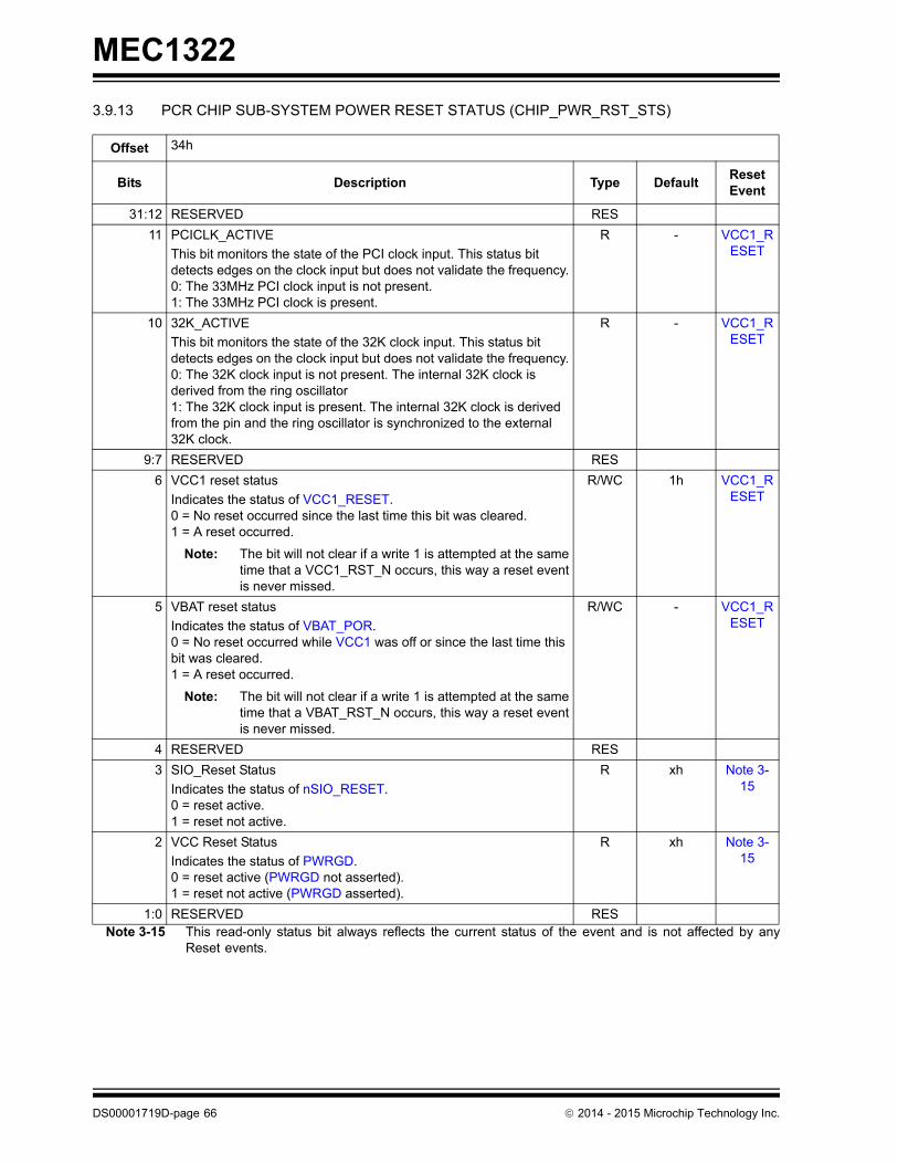
MEC1322
3.9.13 PCR CHIP SUB-SYSTEM POWER RESET STATUS (CHIP_PWR_RST_STS)
Note 3-15 This read-only status bit always reflects the current status of the event and is not affected by anyReset events.
Offset 34h
Bits Description Type DefaultReset Event
31:12 RESERVED RES
11 PCICLK_ACTIVE
This bit monitors the state of the PCI clock input. This status bit detects edges on the clock input but does not validate the frequency.0: The 33MHz PCI clock input is not present.1: The 33MHz PCI clock is present.
R - VCC1_RESET
10 32K_ACTIVE
This bit monitors the state of the 32K clock input. This status bit detects edges on the clock input but does not validate the frequency.0: The 32K clock input is not present. The internal 32K clock is derived from the ring oscillator1: The 32K clock input is present. The internal 32K clock is derived from the pin and the ring oscillator is synchronized to the external 32K clock.
R - VCC1_RESET
9:7 RESERVED RES
6 VCC1 reset status
Indicates the status of VCC1_RESET.0 = No reset occurred since the last time this bit was cleared.1 = A reset occurred.
Note: The bit will not clear if a write 1 is attempted at the sametime that a VCC1_RST_N occurs, this way a reset eventis never missed.
R/WC 1h VCC1_RESET
5 VBAT reset status
Indicates the status of VBAT_POR.0 = No reset occurred while VCC1 was off or since the last time this bit was cleared.1 = A reset occurred.
Note: The bit will not clear if a write 1 is attempted at the sametime that a VBAT_RST_N occurs, this way a reset eventis never missed.
R/WC - VCC1_RESET
4 RESERVED RES
3 SIO_Reset Status
Indicates the status of nSIO_RESET.0 = reset active.1 = reset not active.
R xh Note 3-15
2 VCC Reset Status
Indicates the status of PWRGD.0 = reset active (PWRGD not asserted).1 = reset not active (PWRGD asserted).
R xh Note 3-15
1:0 RESERVED RES
DS00001719D-page 66 2014 - 2015 Microchip Technology Inc.

MEC1322
3.9.14 CHIP RESET ENABLE REGISTER (CHIP_RST_EN)
3.9.15 HOST RESET ENABLE REGISTER (HOST_RST_EN)
Offset 38h
Bits Description Type DefaultReset Event
31:2 RESERVED RES
1 MCHP Reserved R 0h VCC1_RESET
0 MCHP Reserved R/W 0h VCC1_RESET
Note: If a block is configured such that it is to be reset when it goes to sleep, then registers within the block maynot be writable when the block is asleep.
Offset 3Ch
Bits Description Type DefaultReset Event
31:19 RESERVED RES
18 RTC Reset Enable
0: block will not be reset on sleep.1: block will be reset on sleep.
R/W 0h VCC1_RESET
17 RESERVED RES
16 8042EM Reset Enable
0: block will not be reset on sleep.1: block will be reset on sleep.
R/W 0h VCC1_RESET
15 ACPI PM1 Reset Enable
0: block will not be reset on sleep.1: block will be reset on sleep.
R/W 0h VCC1_RESET
14 ACPI EC 1 Reset Enable
0: block will not be reset on sleep.1: block will be reset on sleep.
R/W 0h VCC1_RESET
13 ACPI EC 0 Reset Enable
0: block will not be reset on sleep.1: block will be reset on sleep.
R/W 0h VCC1_RESET
12 GLBL_CFG Reset Enable
0: block will not be reset on sleep.1: block will be reset on sleep.
R/W 0h VCC1_RESET
11:2 RESERVED RES
1 UART 0 Reset Enable
0: block will not be reset on sleep.1: block will be reset on sleep.
R/W 0h VCC1_RESET
0 LPC Reset Enable
0: block will not be reset on sleep.1: block will be reset on sleep.
R/W 0h VCC1_RESET
Note: If a block is configured such that it is to be reset when it goes to sleep, then registers within the block maynot be writable when the block is asleep.
2014 - 2015 Microchip Technology Inc. DS00001719D-page 67

MEC1322
3.9.16 EC RESET ENABLE REGISTER (EC_RST_EN)
Offset 40h
Bits Description Type DefaultReset Event
31 TIMER16_1 Reset Enable
0: block will not be reset on sleep.1: block will be reset on sleep.
R/W 0h VCC1_RESET
30 TIMER16_0 Reset Enable
0: block will not be reset on sleep.1: block will be reset on sleep.
R/W 0h VCC1_RESET
29 EC_REG_BANK Reset Enable
0: block will not be reset on sleep.1: block will be reset on sleep.
R/W 0h VCC1_RESET
28:23 RESERVED RES
22 PWM3 Reset Enable
0: block will not be reset on sleep.1: block will be reset on sleep.
R/W 0h VCC1_RESET
21 PWM2 Reset Enable
0: block will not be reset on sleep.1: block will be reset on sleep.
R/W 0h VCC1_RESET
20 PWM1 Reset Enable
0: block will not be reset on sleep.1: block will be reset on sleep.
R/W 0h VCC1_RESET
19:12 RESERVED RES
11 TACH1 Reset Enable
0: block will not be reset on sleep.1: block will be reset on sleep.
R/W 0h VCC1_RESET
10 SMB0 Reset Enable
0: block will not be reset on sleep.1: block will be reset on sleep.
R/W 0h VCC1_RESET
9 WDT Reset Enable
0: block will not be reset on sleep.1: block will be reset on sleep.
R/W 0h VCC1_RESET
8 PROCESSOR Sleep Enable
0: block will not be reset on sleep.1: block will be reset on sleep.
R/W 0h VCC1_RESET
7 TFDP Reset Enable
0: block will not be reset on sleep.1: block will be reset on sleep.
R/W 0h VCC1_RESET
6 DMA Reset Enable
0: block will not be reset on sleep.1: block will be reset on sleep.
R/W 0h VCC1_RESET
5 PMC Reset Enable
0: block will not be reset on sleep.1: block will be reset on sleep.
R/W 0h VCC1_RESET
4 PWM0 Reset Enable
0: block will not be reset on sleep.1: block will be reset on sleep.
R/W 0h VCC1_RESET
DS00001719D-page 68 2014 - 2015 Microchip Technology Inc.

MEC1322
3.9.17 EC RESET ENABLE 2 REGISTER (EC_RST_EN2)
3 RESERVED RES
2 TACH0 Reset Enable
0: block will not be reset on sleep.1: block will be reset on sleep.
R/W 0h VCC1_RESET
1 PECI Reset Enable
0: block will not be reset on sleep.1: block will be reset on sleep.
R/W 0h VCC1_RESET
0 INT Reset Enable
0: block will not be reset on sleep.1: block will be reset on sleep.
R/W 0h VCC1_RESET
Note: If a block is configured such that it is to be reset when it goes to sleep, then registers within the block maynot be writable when the block is asleep.
Offset 44h
Bits Description Type DefaultReset Event
31:29 RESERVED RES
28 MCHP Reserved R/W 0h VCC1_RESET
27 MCHP Reserved R/W 0h VCC1_RESET
26 MCHP Reserved R/W 0h VCC1_RESET
25 LED3 Reset Enable
0: block will not be reset on sleep.1: block will be reset on sleep.
R/W 0h VCC1_RESET
24 TIMER32_1 Reset Enable
0: block will not be reset on sleep.1: block will be reset on sleep.
R/W 0h VCC1_RESET
23 TIMER32_0 Reset Enable
0: block will not be reset on sleep.1: block will be reset on sleep.
R/W 0h VCC1_RESET
22 TIMER16_3 Reset Enable
0: block will not be reset on sleep.1: block will be reset on sleep.
R/W 0h VCC1_RESET
21 TIMER16_2_Reset Enable
0: block will not be reset on sleep.1: block will be reset on sleep.
R/W 0h VCC1_RESET
20 SPI1 Reset Enable
0: block will not be reset on sleep.1: block will be reset on sleep.
R/W 0h VCC1_RESET
Offset 40h
Bits Description Type DefaultReset Event
2014 - 2015 Microchip Technology Inc. DS00001719D-page 69

MEC1322
19 BCM Reset Enable
0: block will not be reset on sleep.1: block will be reset on sleep.
R/W 0h VCC1_RESET
18 LED2 Reset Enable
0: block will not be reset on sleep.1: block will be reset on sleep.
R/W 0h VCC1_RESET
17 LED1 Reset Enable
0: block will not be reset on sleep.1: block will be reset on sleep.
R/W 0h VCC1_RESET
16 LED0 Reset Enable
0: block will not be reset on sleep.1: block will be reset on sleep.
R/W 0h VCC1_RESET
15 SMB3 Reset Enable
0: block will not be reset on sleep.1: block will be reset on sleep.
R/W 0h VCC1_RESET
14 SMB2 Reset Enable
0: block will not be reset on sleep.1: block will be reset on sleep.
R/W 0h VCC1_RESET
13 SMB1 Reset Enable
0: block will not be reset on sleep.1: block will be reset on sleep.
R/W 0h VCC1_RESET
12 RPM-PWM Reset Enable
0: block will not be reset on sleep.1: block will be reset on sleep.
R/W 0h VCC1_RESET
11 KEYSCAN Reset Enable
0: block will not be reset on sleep.1: block will be reset on sleep.
R/W 0h VCC1_RESET
10 HTIMER Reset Enable
0: block will not be reset on sleep.1: block will be reset on sleep.
R/W 0h VCC1_RESET
9 SPI0 Reset Enable0: block is free to use clocks as necessary.1: block is commanded to sleep at next available moment.
R/W 0h VCC1_RESET
8 PS2_3 Reset Enable
0: block will not be reset on sleep.1: block will be reset on sleep.
R/W 0h VCC1_RESET
7 PS2_2 Reset Enable
0: block will not be reset on sleep.1: block will be reset on sleep.
R/W 0h VCC1_RESET
6 PS2_1 Reset Enable
0: block will not be reset on sleep.1: block will be reset on sleep.
R/W 0h VCC1_RESET
5 PS2_0 Reset Enable
0: block will not be reset on sleep.1: block will be reset on sleep.
R/W 0h VCC1_RESET
4 MCHP Reserved
R/W 0h VCC1_RESET
Offset 44h
Bits Description Type DefaultReset Event
DS00001719D-page 70 2014 - 2015 Microchip Technology Inc.

MEC1322
3.9.18 POWER RESET CONTROL (PWR_RST_CTRL) REGISTER
3 ADC Reset Enable
0: block will not be reset on sleep.1: block will be reset on sleep.
R/W 0h VCC1_RESET
2:0 RESERVED RES
Note: If a block is configured such that it is to be reset when it goes to sleep, then registers within the block maynot be writable when the block is asleep.
Offset 48h
Bits Description Type DefaultReset Event
31:1 RESERVED RES
0 iRESET_OUT
The iRESET_OUT bit is used by firmware to control the internal nSIO_RESET signal function and the external nRESET_OUT pin. The external pin nRESET_OUT is always driven by nSIO_RESET. Firmware can program the state of iRESET_OUT except when the VCC PWRGD bit is not asserted (‘0’), in which case iRESET_OUT is ‘don’t care’ and nSIO_RESET is asserted (‘0’) (TABLE 3-11:).
The internal nSIO_RESET signal is asserted when iRESET_OUT is asserted even if the nRESET_OUT pin is configured as an alternate function.
The iRESET_OUT bit must be cleared to take the Host out of reset.
R/W 1h VCC1_RESET
TABLE 3-11: iRESET_OUT BIT BEHAVIOR
VCC PWRGD iRESET_OUTnSIO_RESET & nRESET_OUT
Description
0 X 0 (ASSERTED) The iRESET_OUT bit does not affect the state of nSIO_RESET when VCC PWRGD is not asserted.
1 1 0 (ASSERTED) The iRESET_OUT bit can only be written by firmware when VCC PWRGD is asserted.0 1 (NOT
ASSERTED)
Offset 44h
Bits Description Type DefaultReset Event
2014 - 2015 Microchip Technology Inc. DS00001719D-page 71

MEC1322
4.0 VBAT REGISTER BANK
4.1 Introduction
This chapter defines a bank of registers powered by VBAT.
4.2 Interface
This block is designed to be accessed internally by the EC via the register interface.
4.3 Power, Clocks and Reset
This section defines the Power, Clock, and Reset parameters of the block.
4.3.1 POWER DOMAINS
4.3.2 CLOCK INPUTS
This block does not require any special clock inputs. All register accesses are synchronized to the host clock.
4.3.3 RESETS
4.4 Interrupts
4.5 Low Power Modes
The VBAT Register Bank is designed to always operate in the lowest power consumption state.
4.6 Description
The VBAT Register Bank block is a block implemented for aggregating miscellaneous battery-backed registers requiredthe host and by the Embedded Controller (EC) Subsystem that are not unique to a block implemented in the EC sub-system.
4.7 EC-Only Registers
Note 4-1 The Base Address indicates where the first register can be accessed in a particular address spacefor a block instance.
TABLE 4-1: POWER SOURCES
Name Description
VBAT The VBAT Register Bank are all implemented on this single power domain.
TABLE 4-2: RESET SIGNALS
Name Description
VBAT_POR This reset signal, which is an input to this block, resets all the logic and registers to their initial default state.
TABLE 4-3: INTERRUPT SIGNALS
Name Description
PFR_Status This interrupt signal from the Power-Fail and Reset Status Register indicates VBAT RST and WDT events.
TABLE 4-4: EC-ONLY REGISTER BASE ADDRESS TABLE
Block InstanceInstance Number
Host Address Space Base Address (Note 4-1)
VBAT_REG_BANK 0 EC 32-bit internal address space
4000A400h
DS00001719D-page 72 2014 - 2015 Microchip Technology Inc.

MEC1322
4.7.1 POWER-FAIL AND RESET STATUS REGISTER
The Power-Fail and Reset Status Register collects and retains the VBAT RST and WDT event status when VCC1 isunpowered.
4.7.2 CLOCK ENABLE REGISTER
APPLICATION NOTE: The XOSEL bit should be correctly configured by firmware before the 32K_EN bit isassserted.
TABLE 4-5: RUNTIME REGISTER SUMMARY
Offset Register Name
00h Power-Fail and Reset Status Register
04h MCHP Reserved
08h Clock Enable Register
Address 00h
Bits Description Type DefaultReset Event
7 VBAT_RSTThe VBAT RST bit is set to ‘1’ by hardware when a VBAT_POR is detected. This is the register default value. To clear VBAT RST EC firmware must write a ‘1’ to this bit; writing a ‘0’ to VBAT RST has no affect.
R/WC 1 VBAT_POR
6 Reserved RES - -
5 WDTThe WDT bit is asserted (‘1’) following a Watch-Dog Timer Forced Reset (WDT Event). To clear the WDT bit EC firmware must write a ‘1’ to this bit; writing a ‘0’ to the WDT bit has no affect.
R/WC 0 VBAT_POR
4:1 Reserved RES - -
0 DET32K_IN0 = No clock detected on the XTAL[1:2] pins.1= Clock detected on the XTAL[1:2] pins.
R X VBAT_POR
Address 08h
Bits Description Type DefaultReset Event
31:2 RESERVED RES - -
1 32K_EN
This bit controls the 32.768 KHz Crystal Oscillator as defined in TABLE 4-6:.
R/W 0b VBAT_POR
0 XOSEL
This bit controls whether a crystal or single ended clock source is used.1= the 32.768 KHz Crystal Oscillator is driven by a single-ended 32.768 KHz clock source connected to the XTAL2 pin.0= the 32.768 KHz Crystal Oscillator requires a 32.768 KHz parallel resonant crystal connected between the XTAL1 and XTAL2 pins (default).
R/W 0b VBAT_POR
2014 - 2015 Microchip Technology Inc. DS00001719D-page 73

MEC1322
Note 4-2 the 48MHz Ring Oscillator must not stop before 40 μs min after the 32K_EN bit is asserted.
TABLE 4-6: 32K_EN BIT
32K_EN 32.768 KHz Crystal Oscillator Description
0 OFF VBAT_POR default.
1 ON The 32.768 KHz Crystal Oscillator can only be enabled by firmware (Note 4-2).
DS00001719D-page 74 2014 - 2015 Microchip Technology Inc.
MEC1322
5.0 LPC INTERFACE
5.1 Introduction
The Intel® Low Pin Count (LPC) Interface is the LPC Interface used by the system host to configure the chip and com-municate with the logical devices implemented in the design through a series of read/write registers. Register access isaccomplished through the LPC transfer cycles defined in Table 5-8, "LPC Cycle Types Supported".
The Logical Devices implemented in the design are identified in Table 5-16, “I/O Base Address Registers,” on page 92.The Base Address Registers allow any logical device’s runtime registers to be relocated in LPC I/O space. All chip con-figuration registers for the device are accessed indirectly through the LPC I/O Configuration Port (see Section 5.8.3,"Configuration Port," on page 83).
LPC memory cycles may also be used to access the Base Address Registers of certain devices.
5.2 References
• Intel® Low Pin Count (LPC) Interface Specification, v1.1
• PCI Local Bus Specification, Rev. 2.2
• Serial IRQ Specification for PCI Systems Version 6.0.
• PCI Mobile Design Guide Rev 1.0
5.3 Terminology
This table defines specialized terms localized to this feature.
TABLE 5-1: TERMINOLOGY
Term Definition
System Host Refers to the external CPU that communicates with this device via the LPC Interface.
Logical Devices Logical Devices are LPC accessible features that are allocated a Base Address and range in LPC I/O address space
Runtime Register Runtime Registers are register that are directly I/O accessible by the System Host via the LPC interface. These registers are defined in Section 5.10, "Runtime Registers," on page 93.
Configuration Registers Registers that are only accessible in CONFIG_MODE. These registers are defined in Section 5.9, "LPC Configuration Registers," on page 88.
EC_Only Registers Registers that are not accessible by the System Host. They are only accessible by an internal embedded controller. These registers are defined in Section 5.11, "EC-Only Registers," on page 94.
2014 - 2015 Microchip Technology Inc. DS00001719D-page 75

MEC1322
5.4 Interface
This block is designed to be accessed externally via the pin interface and internally via a registered host interface.
5.4.1 SIGNAL DESCRIPTION
FIGURE 5-1: BLOCK DIAGRAM OF LPC INTERFACE CONTROLLER WITH CLKRUN# SUPPORT
TABLE 5-2: SIGNAL DESCRIPTION TABLE
Name Direction Description
LAD0 Input/Output Bit[0] of the LPC multiplexed command, address, and data bus.
LAD1 Input/Output Bit[1] of the LPC multiplexed command, address, and data bus.
LAD2 Input/Output Bit[2] of the LPC multiplexed command, address, and data bus.
LAD3 Input/Output Bit[3] of the LPC multiplexed command, address, and data bus.
SERIRQ
LAD0
LAD1
LAD2
LAD3
LFRAME#
LRESET#
LCLK
LPC Interface(Logical Device Ch)
LPC Controller
Serial IRQState MachineInterface to
Configuration Registers
Con
figur
atio
n P
ort
CLKRUN#
LPC Config Registers
LPC Regis-ters
(Runtime, EC-Only)
Interface to Logical Device Register
DS00001719D-page 76 2014 - 2015 Microchip Technology Inc.

MEC1322
5.4.2 REGISTER INTERFACES
The registers defined for the LPC Interface block are accessible by the various hosts as indicated in Section 5.9, "LPCConfiguration Registers", Section 5.11, "EC-Only Registers"and Section 5.10, "Runtime Registers".
5.5 Power, Clocks and Reset
This section defines the Power, Clock, and Reset parameters of the block.
5.5.1 POWER DOMAINS
5.5.2 CLOCK INPUTS
5.5.3 RESETS
The following table defines the effective reset state that result from the combination of these three reset signals.
LFRAME# Input Active low signal indicates start of new cycle and termina-tion of broken cycle.
LRESET# Input Active low signal used as LPC Interface Reset. Same as PCI Reset on host.
Note: LRESET# is typically connected to the hostPCI RESET (PCIRST#) signal.
LCLK Input PCI clock input (PCI_CLK)
SERIRQ Input/Output Serial IRQ pin used with the LCLK signal to transfer inter-rupts to the host.
CLKRUN# Open-Drain Output Clock Control for LCLK
TABLE 5-3: POWER SOURCES
Name Description
VCC1 The LPC Interface block and registers are powered by VCC1.
TABLE 5-4: CLOCK INPUTS
Name Description
LCLK This LPC Interface has a single clock input, called LCLK.
Note: The PCI_CLK input to LCLK can run at 19.2MHz to 33MHz. When the PCI_CLK input frequency is from19.2MHz (including 24MHz) to 33MHz the Handshake bit in the EC Clock Control Register must be set toa ‘1’ to capture LPC transactions properly. See Section 5.11.4, "EC Clock Control Register," on page 96.
TABLE 5-5: RESET SIGNALS
Name Description
VCC1_RESET Power on Reset to the block. This signal resets all the register and logic in this block to its default state.
nSIO_RESET This signal is used to indicate when the main power rail in the system is reset. The LPC interface is operational when main power is present. This signal is used to reset selected registers as defined in the Register Interfaces descriptions.
LRESET# The LRESET# signal comes from the LPC pin interface. This signal is defined in the Intel® Low Pin Count (LPC) Interface Specification, v1.1.
TABLE 5-2: SIGNAL DESCRIPTION TABLE (CONTINUED)
Name Direction Description
2014 - 2015 Microchip Technology Inc. DS00001719D-page 77

MEC1322
Note 5-1 The EC can determine the state of the LRESET# input using registers in LPC Bus Monitor Registeron page 95.
Note 5-2 VCC1_RESET is asserted when VCC1 is turned off and is released after VCC1 is turned on. TheVCC1_RESET will be released before the System Host is expected to attempt communication overthe LPC Interface.
Note 5-3 See the individual register descriptions to determine which registers are effected by nSIO_RESET.
Note 5-4 The LPC Interface will be ready to receive a new transaction when LRESET# is deasserted. See theindividual register descriptions to determine which registers are effected by this reset.
In system, the LPC Interface is required to be operational in ACPI Sleep States S0 - S2. When the system enters SleepStates S3 - S5 the LPC interface must tristate its outputs. The following table shows the behavior of LPC output andinput/output signals under reset conditions.
5.6 Interrupts
This section defines the Interrupt Sources generated from this block.
5.7 Low Power Modes
The LPC Controller may be put into a low power state by the chip’s Power, Clocks, and Reset (PCR) circuitry.
The LPC Block has implemented an EC Clock Control Register to determine how the internal clocks are effected by thesupported low power modes. See Section 5.11.4, "EC Clock Control Register," on page 96 for a description of theseoptions.
5.8 Description
This LPC Controller is compliant with the Intel® Low Pin Count (LPC) Interface Specification, v1.1. Section 5.8.1, "LPCController Description" further clarifies which LPC Interface features have been implemented and qualifies any systemspecific requirements.
TABLE 5-6: LPC Interface BLOCK RESET STATES
VCC1_RESET(Note 5-2)
LRESET#(Note 5-1, Note 5-4)
nSIO_RESET(Note 5-3)
Reset State
Asserted X X Resets all registers and logic
Deasserted Asserted X Resets selected registers and logic
Deasserted Asserted Resets selected registers
Deasserted Nothing is in Reset
Note: See Section 5.8.1.3, "LPC Clock Run," on page 80 page 157 for LPC protocol dependent pin state transi-tions requirements.
TABLE 5-7: LPC INTERFACE SIGNALS BEHAVIOR ON RESET
Pins VCC1_RESET nSIO_RESETLRESET#Asserted
LAD[3:0] Tri-state Tri-state Tri-State
SERIRQ Tri-state Tri-state Tri-State
CLKRUN# Tri-state Tri-state Tri-State
Source Description
LPC_INTERNAL_ERR The LPC_INTERNAL_ERR event is sourced by bit D0 of the Host Bus Error Register.
DS00001719D-page 78 2014 - 2015 Microchip Technology Inc.

MEC1322
The LPC Controller claims only LPC transactions targeted for one of its peripherals. Section 5.8.2, on page 81,describes the mechanism for Claiming and Forwarding Transactions for Supported LPC Cycles. LPC transactions maybe used to configure the chip and to access registers during operation. The mechanism to configure the chip isdescribed in Section 5.8.3, "Configuration Port," on page 83.
LPC memory cycles may also be used to access the Base Address Registers of certain devices.
Once configured, the LPC peripherals implemented as logical devices on chip may use the SERIRQ to notify the hostof an event. See Section 5.8.4, "Serial IRQs," on page 84.
5.8.1 LPC CONTROLLER DESCRIPTION
The following sections qualify the LPC features implemented according to the LPC Specification.
5.8.1.1 Cycle Types Supported
The following cycle types are supported by the LPC Interface Controller. All other cycles that it does not support areignored.
When the LPC Controller detects a transaction targeted for this device it claims and forwards that transaction as definedin Section 5.8.2, "Claiming and Forwarding Transactions for Supported LPC Cycles," on page 81.
LPC I/O CYCLES
The system host may use LPC I/O cycles to read/write the I/O mapped configuration and runtime registers implementedin this device. See the Intel® Low Pin Count (LPC) Interface Specification, v1.1, Section 5.2 for definition of LPC I/OCycles.
LPC MEMORY CYCLES
The system host may use LPC memory cycles to access memory mapped registers implemented in this device. Seethe Intel® Low Pin Count (LPC) Interface Specification, v1.1, Section 5.1 for definition of LPC Memory Cycles.
5.8.1.2 LAD[3:0] Fields
The LAD[3:0] signals support multiple fields for each protocol as defined in section 4.2.1 LAD[3:0] of the Intel® Low PinCount (LPC) Interface Specification, v1.1. The following sections further qualify the fields supported.
WAIT SYNCS ON LPC
LPC transactions that access registers located on the device require a minimum of two wait SYNCs on the LPC bus.The number of SYNCs may be larger if the internal bus is in use by the embedded controller, of if the data referencedby the host is not present in a register. The device always uses Long Wait SYNCs, rather than Short Wait SYNCs, whenresponding to an LPC bus request.
ERROR SYNCS ON LPC
The device does not issue ERROR SYNC cycles.
TABLE 5-8: LPC CYCLE TYPES SUPPORTED
Cycle Type Transfer Size
I/O Read 1 byte
I/O Write 1 byte
Memory Read 1 byte
Memory Write 1 byte
Note: All LPC transactions are synchronized to the LCLK and will complete with a maximum of 8 wait states,unless otherwise noted.
2014 - 2015 Microchip Technology Inc. DS00001719D-page 79

MEC1322
5.8.1.3 LPC Clock Run
USING CLKRUN#
CLKRUN# is used to indicate the status of LCLK as well as to request that a stopped clock be started. See FIGURE5-2: CLKRUN# System Implementation Example on page 81, an example of a typical system implementation usingCLKRUN#.
LCLK Run Support can be enabled and disabled via SIRQ_MODE as shown in Table 5-9, "LPC Controller CLKRUN#Function". When the SIRQ_MODE is ‘0,’ Serial IRQs are disabled, the CLKRUN# pin is disabled, and the affects of Inter-rupt requests on CLKRUN# are ignored. When the SIRQ_MODE is ‘1,’ Serial IRQs are enabled, the CLKRUN# pin isenabled, and the CLKRUN# support related to Interrupts requests as described in the section below is enabled.
The CLKRUN# pin is an open drain output and input. Refer to the PCI Mobile Design Guide Rev 1.0 for a descriptionof the CLKRUN# function. If CLKRUN# is sampled “high”, LCLK is stopped or stopping. If CLKRUN# is sampled “low”,LCLK is starting or started (running).
CLKRUN# Support for Serial IRQ Cycle
If a logical device asserts or de-asserts an interrupt and CLKRUN# is sampled “high”, the LPC Controller can requestthe restoration of the clock by asserting the CLKRUN# signal asynchronously (Table 5-9). The LPC Controller holdsCLKRUN# low until it detects two rising edges of the clock. After the second clock edge, the controller must disable theopen drain driver (Figure 5-3).
The LPC Controller must not assert CLKRUN# if it is already driven low by the central resource; i.e., the PCI CLOCKGENERATOR in Figure 5-2. The controller does not assert CLKRUN# under any conditions if the Serial IRQs are dis-abled.
The LPC Controller must not assert CLKRUN# unless the line has been de-asserted for two successive clocks; i.e.,before the clock was stopped (Figure 5-3).
The LPC Controller does not assert CLKRUN# if it is already driven low by the central resource; i.e., the PCI CLOCKGENERATOR. The LPC Controller also does not assert CLKRUN# unless the signal has been de-asserted for twosuccessive clocks; i.e., before the clock was stopped.
Note 5-5 SIRQ_MODE is defined in Section 5.8.4.1, "Enabling SERIRQ Function," on page 84.
Note 5-6 “Change” means either-edge change on any or all parallel IRQs routed to the Serial IRQ block. The“change” detection logic must run asynchronously to LCLK and regardless of the Serial IRQ mode;i.e., “continuous” or “quiet”.
TABLE 5-9: LPC CONTROLLER CLKRUN# FUNCTION
SIRQ_MODE (Note 5-5)
Internal InterruptOr DMA Request
CLKRUN# Action
0 X X None
1 NO CHANGE X None
CHANGE (Note 5-6) 0 None
1 Assert CLKRUN#
DS00001719D-page 80 2014 - 2015 Microchip Technology Inc.
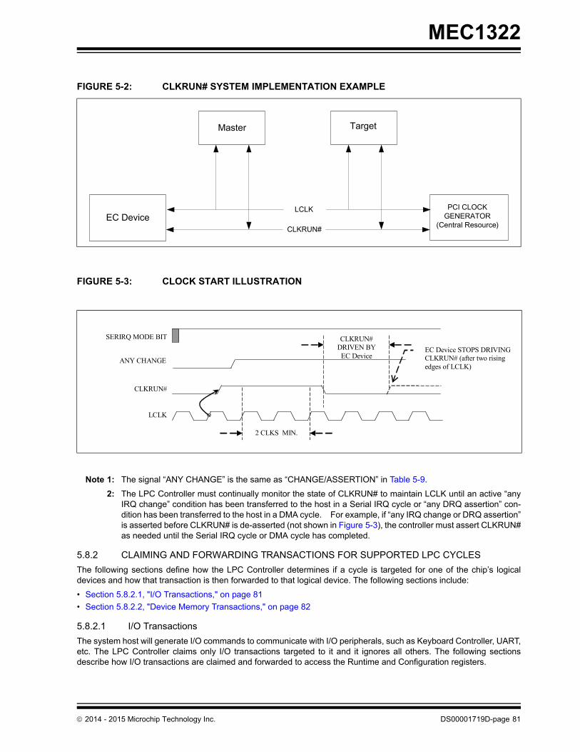
MEC1322
FIGURE 5-3: CLOCK START ILLUSTRATION
Note 1: The signal “ANY CHANGE” is the same as “CHANGE/ASSERTION” in Table 5-9.
2: The LPC Controller must continually monitor the state of CLKRUN# to maintain LCLK until an active “anyIRQ change” condition has been transferred to the host in a Serial IRQ cycle or “any DRQ assertion” con-dition has been transferred to the host in a DMA cycle. For example, if “any IRQ change or DRQ assertion”is asserted before CLKRUN# is de-asserted (not shown in Figure 5-3), the controller must assert CLKRUN#as needed until the Serial IRQ cycle or DMA cycle has completed.
5.8.2 CLAIMING AND FORWARDING TRANSACTIONS FOR SUPPORTED LPC CYCLES
The following sections define how the LPC Controller determines if a cycle is targeted for one of the chip’s logicaldevices and how that transaction is then forwarded to that logical device. The following sections include:
• Section 5.8.2.1, "I/O Transactions," on page 81
• Section 5.8.2.2, "Device Memory Transactions," on page 82
5.8.2.1 I/O Transactions
The system host will generate I/O commands to communicate with I/O peripherals, such as Keyboard Controller, UART,etc. The LPC Controller claims only I/O transactions targeted to it and it ignores all others. The following sectionsdescribe how I/O transactions are claimed and forwarded to access the Runtime and Configuration registers.
FIGURE 5-2: CLKRUN# SYSTEM IMPLEMENTATION EXAMPLE
CLKRUN#
LCLK
Target
PCI CLOCKGENERATOR
(Central Resource)
Master
EC Device
LCLK
CLKRUN#
SERIRQ MODE BIT
ANY CHANGE
CLKRUN# DRIVEN BY
EC Device EC Device STOPS DRIVING CLKRUN# (after two rising edges of LCLK)
2 CLKS MIN.
2014 - 2015 Microchip Technology Inc. DS00001719D-page 81

MEC1322
CLAIMING LPC I/O TRANSACTIONS
The LPC Controller claims an I/O transaction that is targeted for one of its peripherals (also referred to as logicaldevices). A Base Address Register has been implemented for each logical device. See Section 5.9.3, "I/O Base AddressRegisters (BARs)," on page 91. If one of the addresses programmed in the Logical Device Base Address Registersmatches an LPC I/O address using the following relationship, the LPC Controller will claim the LPC bus cycle:
(LPC Address & ~BAR.MASK) == (BAR.LPC_Address & ~BAR.MASK) && (BAR.Valid == 1)
FORWARDING I/O TRANSACTIONS
The system host will use I/O transactions to access the Configuration and Runtime registers.
To access the Runtime registers, the host must configure the I/O Base Address Registers (BARs), which are accessiblevia the Configuration Port. The Configuration Port, Logical Device Ch, is located at the Base I/O Address programmedin the BAR Configuration register located at offset 60h.
If the I/O transaction matches the BAR of Logical Device Ch, the transaction will be forwarded to the Configuration Port,otherwise the transaction will be forwarded to the Runtime Registers of the targeted logical device.
Each Logical Device may have up to 128 Contiguous Runtime Registers. The Runtime Registers are located at adefined offset from the Logical Device’s base address. The host can directly access these registers with a standard LPCI/O command.
The Logical Device number for the matching device is located in the Frame field of the BAR.When matching LPC I/O addresses, the LPC Controller ignores address bits that correspond to ‘1b’ bits in the MASKfield.
For illustration purposes only, lets examine two types of logical devices (these may or may not reside in this design).
Example 1:
The Keyboard Controller (8042 Interface) Base Address Register has 60h in the LPC Address field, the Frame field is01h, and the MASK field is 04h. Because of the single ‘1b’ bit in MASK, the BAR will match LPC I/O patterns in the form‘0000_0000_0110_0x00b’, so both 60h and 64h will be matched and claimed by the LPC Controller.
Example 2:
If a standard 16550 UART was located at LPC I/O address 238h, then the UART Receive buffer would appear ataddress 238h and the Line Status register at 23Dh. If the BAR for the UART was set to 0238_8047h, then the UARTwill be matched at I/O address 238h.
5.8.2.2 Device Memory Transactions
Alternatively, LPC memory transactions can be used to access certain logical devices. The LPC Controller claims amemory transaction that is targeted for one of these logical devices. A Device Memory Base Address Register has beenimplemented for the logical devices listed in Table 5-17, “Device Memory Base Address Register Default Values,” onpage 93.
On every LPC bus Memory access all Base Address Registers are checked in parallel and if any matches the LPC mem-ory address the MEC1322 claims the bus cycle. The memory address is claimed as described in I/O Transactionsexcept that the LPC memory cycle address is 32 bits instead of the 16 bit I/O cycle address.
Software should insure that no two BARs map the same LPC memory address. If two BARs do map to the sameaddress, the BAR_Conflict bit in the Host Bus Error Register is set when an LPC access targeting the BAR Conflictaddress. An EC interrupt can be generated.
Each Device Memory BAR is 48 bits wide. The format of each Device Memory BAR is summarized in Device MemoryBase Address Register Format. An LPC memory request is translated by the Device Memory BAR into an 8-bit read orwrite transaction on the AHB bus. The 32-bit LPC memory address is translated into a 24-bit AHB address
The Base Address Register Table is itself part of the AHB address space. It resides in the Configuration quadrant ofLogical Device Ch, the LPC Interface.
Note: The LPC Controller’s Base Address register is used to define the Base I/O Address of the ConfigurationPort.
DS00001719D-page 82 2014 - 2015 Microchip Technology Inc.
MEC1322
5.8.3 CONFIGURATION PORT
The LPC Host can access the Chip’s Configuration Registers through the Configuration Port when CONFIG MODE isenabled. The device defaults to CONFIG MODE being disabled.
The Configuration Port is composed of an INDEX and DATA Register. The INDEX register is used as an address pointerto an 8-bit configuration register and the DATA register is used to read or write the data value from the indexed config-uration register. Once CONFIG MODE is enabled, reading the Configuration Port Data register will return the data valuethat is in the indexed Configuration Register.
If no value was written to the INDEX register, reading the Data Register in the Configuration Port will return the value inConfiguration Address location 00h (default).
Note 5-7 The default Base I/O Address of the Configuration Port can be relocated by programming the BARregister for Logical Device Ch (LPC/Configuration Port) at offset 60h. The Relative Address showsthe general case for determining the I/O address for each register.
5.8.3.1 Enable CONFIG MODE
The INDEX and DATA registers are effective only when the chip is in CONFIG MODE. CONFIG MODE is enabled whenthe Config Entry Key is successfully written to the I/O address of the INDEX register of the CONFIG PORT while theCONFIG MODE is disabled (see Section 5.8.3.2, "Disable CONFIG MODE").
Config Entry Key = < 55h>
5.8.3.2 Disable CONFIG MODE
CONFIG MODE defaults to disabled on a VCC1_RESET, nSIO_RESET, and when LRESET# is asserted. CONFIGMODE is also disabled when the following Config Exit Key is successfully written to the I/O address of the INDEX PORTof the CONFIG PORT while CONFIG MODE is enabled.
Config Exit Key = < AAh>
5.8.3.3 Configuration Sequence Example
To program the configuration registers, the following sequence must be followed:
1. Enable Configuration State
2. Program the Configuration Registers
3. Disable Configuration State.
The following is an example of a configuration program in Intel 8086 assembly language.
;----------------------------.; ENABLE CONFIGURATION STATE;----------------------------'MOV DX,CONFIG_PORT_BASE_ADDRESSMOV AX,055H; Config Entry KeyOUT DX,AL;----------------------------.; CONFIGURE BASE ADDRESS, |; LOGICAL DEVICE 8 |;----------------------------'MOV DX,CONFIG_PORT_BASE_ADDRESSMOV AL,07HOUT DX,AL; Point to LD# Config RegMOV DX,CONFIG_PORT_BASE_ADDRESS+1
Note: The data read from the Configuration Port Data register is undefined when CONFIG MODE is not enabled.
TABLE 5-10: CONFIGURATION PORT
Default I/O Address(Note 5-7)
Type Register Name Relative AddressDefault Value
Notes
002Eh Read / Write INDEX Configuration Port’s Base Address + 0 00h Note 5-7
002Fh Read / Write DATA Configuration Port’s Base Address + 1 00h
2014 - 2015 Microchip Technology Inc. DS00001719D-page 83
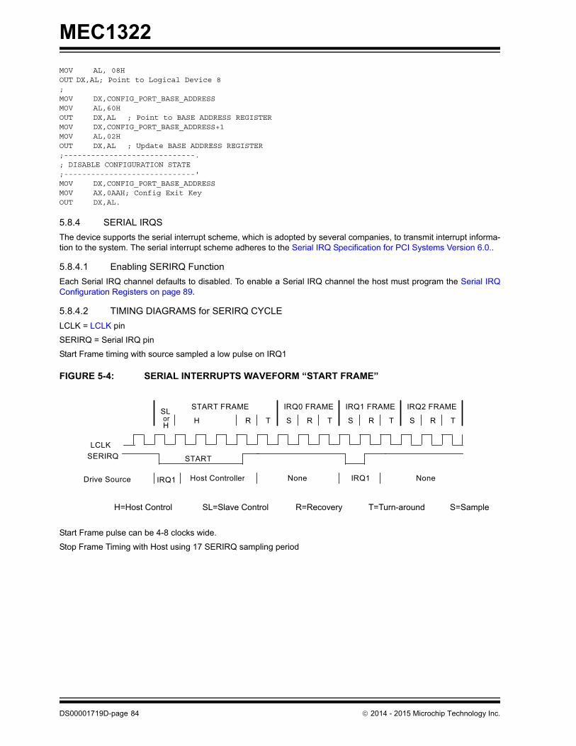
MEC1322
MOV AL, 08HOUT DX,AL; Point to Logical Device 8;MOV DX,CONFIG_PORT_BASE_ADDRESSMOV AL,60HOUT DX,AL ; Point to BASE ADDRESS REGISTERMOV DX,CONFIG_PORT_BASE_ADDRESS+1MOV AL,02HOUT DX,AL ; Update BASE ADDRESS REGISTER;-----------------------------.; DISABLE CONFIGURATION STATE;-----------------------------'MOV DX,CONFIG_PORT_BASE_ADDRESSMOV AX,0AAH; Config Exit KeyOUT DX,AL.
5.8.4 SERIAL IRQS
The device supports the serial interrupt scheme, which is adopted by several companies, to transmit interrupt informa-tion to the system. The serial interrupt scheme adheres to the Serial IRQ Specification for PCI Systems Version 6.0..
5.8.4.1 Enabling SERIRQ Function
Each Serial IRQ channel defaults to disabled. To enable a Serial IRQ channel the host must program the Serial IRQConfiguration Registers on page 89.
5.8.4.2 TIMING DIAGRAMS for SERIRQ CYCLE
LCLK = LCLK pin
SERIRQ = Serial IRQ pin
Start Frame timing with source sampled a low pulse on IRQ1
FIGURE 5-4: SERIAL INTERRUPTS WAVEFORM “START FRAME”
Start Frame pulse can be 4-8 clocks wide.
Stop Frame Timing with Host using 17 SERIRQ sampling period
H=Host Control SL=Slave Control R=Recovery T=Turn-around S=Sample
R T S R T S
SERIRQ
LCLK
Host ControllerIRQ1 IRQ1Drive Source
R T
None
IRQ0 FRAME IRQ1 FRAME
S R T
IRQ2 FRAME
None
START
START FRAME
HSLor H
DS00001719D-page 84 2014 - 2015 Microchip Technology Inc.

MEC1322
FIGURE 5-5: SERIAL INTERRUPT WAVEFORM “STOP FRAME”
Stop pulse is two clocks wide for Quiet mode, three clocks wide for Continuous mode.
There may be none, one, or more Idle states during the Stop Frame.
The next SERIRQ cycle’s Start Frame pulse may or may not start immediately after the turn-around clock of the StopFrame.
5.8.4.3 SERIRQ Cycle Control
SERIRQ START FRAME
There are two modes of operation for the SERIRQ Start Frame.
Quiet (Active) Mode
Any device may initiate a Start Frame by driving the SERIRQ low for one clock, while the SERIRQ is Idle. After drivinglow for one clock, the SERIRQ must immediately be tri-stated without at any time driving high. A Start Frame may notbe initiated while the SERIRQ is active. The SERIRQ is Idle between Stop and Start Frames. The SERIRQ is activebetween Start and Stop Frames. This mode of operation allows the SERIRQ to be Idle when there are no IRQ/Datatransitions which should be most of the time.
Once a Start Frame has been initiated, the host controller will take over driving the SERIRQ low in the next clock andwill continue driving the SERIRQ low for a programmable period of three to seven clocks. This makes a total low pulsewidth of four to eight clocks. Finally, the host controller will drive the SERIRQ back high for one clock then tri-state.
Any SERIRQ Device which detects any transition on an IRQ/Data line for which it is responsible must initiate a StartFrame in order to update the host controller unless the SERIRQ is already in an SERIRQ Cycle and the IRQ/Data tran-sition can be delivered in that SERIRQ Cycle.
Continuous (Idle) Mode
Only the Host controller can initiate a Start Frame to update IRQ/Data line information. All other SERIRQ agents becomepassive and may not initiate a Start Frame. SERIRQ will be driven low for four to eight clocks by host controller. Thismode has two functions. It can be used to stop or idle the SERIRQ or the host controller can operate SERIRQ in a con-tinuous mode by initiating a Start Frame at the end of every Stop Frame.
An SERIRQ mode transition can only occur during the Stop Frame. Upon reset, SERIRQ bus is defaulted to continuousmode, therefore only the host controller can initiate the first Start Frame. Slaves must continuously sample the StopFrames pulse width to determine the next SERIRQ Cycle’s mode.
SERIRQ DATA FRAME
Once a Start Frame has been initiated, the LPC Controller will watch for the rising edge of the Start Pulse and start count-ing IRQ/Data Frames from there. Each IRQ/Data Frame is three clocks: Sample phase, Recovery phase, and Turn-around phase. During the sample phase, the LPC Controller must drive the SERIRQ (SIRQ pin) low, if and only if, itslast detected IRQ/Data value was low. If its detected IRQ/Data value is high, SERIRQ must be left tri-stated. During therecovery phase, the LPC Controller must drive the SERIRQ high, if and only if, it had driven the SERIRQ low during theprevious sample phase. During the turn-around phase, the controller must tri-state the SERIRQ. The device drives theSERIRQ line low at the appropriate sample point if its associated IRQ/Data line is low, regardless of which device initi-ated the start frame.
H=Host Control R=Recovery T=Turn-around S=Sample I= Idle
S R T S
SERIRQ
LCLK
Host ControllerIRQ15Driver
R T
None
IRQ14 IRQ15
S R T
IOCHCK#
None
STOP
R T
STOP FRAME
HI
START
NEXT CYCLE FRAMEFRAMEFRAME
2014 - 2015 Microchip Technology Inc. DS00001719D-page 85

MEC1322
The Sample phase for each IRQ/Data follows the low to high transition of the Start Frame pulse by a number of clocksequal to the IRQ/Data Frame times three, minus one e.g. The IRQ5 Sample clock is the sixth IRQ/Data Frame, then thesample phase is {(6 x 3) - 1 = 17} the seventeenth clock after the rising edge of the Start Pulse.
The SIRQ data frame will now support IRQ2 from a logical device; previously SERIRQ Period 3 was reserved for useby the System Management Interrupt (LSMI#). When using Period 3 for IRQ2, the user should mask off the SMI via theESMI Mask Register. Likewise, when using Period 3 for LSMI#, the user should not configure any logical devices asusing IRQ2.
SERIRQ Period 14 is used to transfer IRQ13. Each Logical devices will have IRQ13 as a choice for their primary inter-rupt.
STOP CYCLE CONTROL
Once all IRQ/Data Frames have completed, the host controller will terminate SERIRQ activity by initiating a Stop Frame.Only the host controller can initiate the Stop Frame. A Stop Frame is indicated when the SERIRQ is low for two or threeclocks. If the Stop Frame’s low time is two clocks, then the next SERIRQ cycle’s sampled mode is the Quiet mode; andany SERIRQ device may initiate a Start Frame in the second clock or more after the rising edge of the Stop Frame’spulse. If the Stop Frame’s low time is three clocks, then the next SERIRQ cycle’s sampled mode is the continuous mode,and only the host controller may initiate a Start Frame in the second clock or more after the rising edge of the StopFrame’s pulse.
5.8.4.4 Latency
Latency for IRQ/Data updates over the SERIRQ bus in bridge-less systems with the minimum IRQ/Data Frames of 17will range up to 96 clocks (3.84μS with a 25 MHz LCLK or 2.88μs with a 33 MHz LCLK).
5.8.4.5 EOI/ISR Read Latency
Any serialized IRQ scheme has a potential implementation issue related to IRQ latency. IRQ latency could cause anEOI or ISR Read to precede an IRQ transition that it should have followed. This could cause a system fault. The hostinterrupt controller is responsible for ensuring that these latency issues are mitigated. The recommended solution is todelay EOIs and ISR Reads to the interrupt controller by the same amount as the SERIRQ Cycle latency in order toensure that these events do not occur out of order.
TABLE 5-11: SERIRQ SAMPLING PERIODS
SERIRQ Period Signal Sampled # of Clocks Past Start
1 Not Used 2
2 IRQ1 5
3 IRQ2 8
4 IRQ3 11
5 IRQ4 14
6 IRQ5 17
7 IRQ6 20
8 IRQ7 23
9 IRQ8 26
10 IRQ9 29
11 IRQ10 32
12 IRQ11 35
13 IRQ12 38
14 IRQ13 41
15 IRQ14 44
16 IRQ15 47
Note: If one or more PCI to PCI Bridge is added to a system, the latency for IRQ/Data updates from the secondaryor tertiary buses will be a few clocks longer for synchronous buses, and approximately double for asyn-chronous buses.
DS00001719D-page 86 2014 - 2015 Microchip Technology Inc.

MEC1322
5.8.4.6 AC/DC Specification Issue
All Serial IRQ agents must drive/sample SERIRQ synchronously related to the rising edge of LCLK. The SERIRQ pinuses the electrical specification of the PCI bus. Electrical parameters will follow the PCI Local Bus Specification, Rev.2.2 definition of “sustained tri-state.”
5.8.4.7 Reset and Initialization
The SERIRQ bus uses LRESET# as its reset signal and follows the PCI bus reset mechanism. The SERIRQ pin is tri-stated by all agents while LRESET# is active. With reset, SERIRQ slaves and bridges are put into the (continuous) Idlemode. The host controller is responsible for starting the initial SERIRQ cycle to collect system’s IRQ/Data default values.The system then follows with the Continuous/Quiet mode protocol (Stop Frame pulse width) for subsequent SERIRQcycles. It is the host controller’s responsibility to provide the default values to the 8259’s and other system logic beforethe first SERIRQ cycle is performed. For SERIRQ system suspend, insertion, or removal application, the host controllershould be programmed into Continuous (IDLE) mode first. This is to ensure the SERIRQ bus is in Idle state before thesystem configuration changes.
5.8.4.8 SERIRQ Interrupts
The LPC Controller routes Logical Device interrupts onto SIRQ stream frames IRQ[0:15]. Routing is controlled by theSIRQ Interrupt Configuration Registers. There is one SIRQ Interrupt Configuration Register for each accessible SIRQFrame (IRQ); all 16 registers are listed in Table 5-15, "SIRQ Interrupt Configuration Register Map".
The format for each SIRQ Interrupt Configuration Register is described in Section 5.9.2.1, "SIRQ Configuration RegisterFormat," on page 90. Each Logical Device can have up to two LPC SERIRQ interrupts. When the device is polled bythe host, each SIRQ frame routes the level of the Logical Device interrupt (selected by the corresponding SIRQ InterruptConfiguration Register) to the SIRQ stream.
5.8.4.9 SERIRQ Routing
Each SIRQ Interrupt Configuration Register controls a series of multiplexers which route to a single Logical Device inter-rupt as illustrated in FIGURE 5-6: SIRQ Routing Internal Logical Devices on page 88. The following table defines theSerial IRQ routing for each logical device implemented in the chip.
TABLE 5-12: LOGICAL DEVICE SIRQ ROUTING
SIRQ Interrupt Configuration Register
Logical Device Interrupt Source
SELECT DEVICE FRAMELogical Device
(Block Instance - Note 1:)Interrupt Source
0 0 0h EMI EC-to-Host
1 0 0h EMI Host Event
0 0 1h 8042 Keyboard Controller KIRQ
1 0 1h 8042 Keyboard Controller MIRQ
0 0 3h ACPI EC0 EC_OBF
0 0 4h ACPI EC1 EC_OBF
0 0 5h ACPI PM1 N/A
0 0 6h Legacy Port92/GateA20 N/A
0 0 7h UART 0 UART
0 0 9h Mailbox MBX_Host SIRQ
1 0 9h Mailbox MBX_Host_SMI
2014 - 2015 Microchip Technology Inc. DS00001719D-page 87

MEC1322
Note 1: The Block Instance number is only included if there are multiple instantiations of a block. Otherwise, single block instances do not require this differentiation.
FIGURE 5-6: SIRQ ROUTING INTERNAL LOGICAL DEVICES
5.9 LPC Configuration Registers
The configuration registers listed in Table 5-14, "Configuration Register Summary" are for a single instance of the LPCInterface. The addresses of each register listed in Table 5-14 are defined as a relative offset to the host “Begin Address”defined in Table 5-13.
0 0 Bh RTC RTC
0 0 Ch LPC interface EC_IRQ
Note: Two Logical Devices cannot share a Serial IRQ.
TABLE 5-12: LOGICAL DEVICE SIRQ ROUTING (CONTINUED)
SIRQ Interrupt Configuration Register
Logical Device Interrupt Source
SELECT DEVICE FRAMELogical Device
(Block Instance - Note 1:)Interrupt Source
0
1 ??????
LD 00h- Int
LD 3Fh- Int
LD 00h-Int0
LD 00h-Int1
0
1
SIRQi Conguration Register[7:0]
Device
Frame
Sel
ect
SERIRQi
Source
8 7 6
0
1
LD 3Fh-Int0
LD 3Fh-Int1
DS00001719D-page 88 2014 - 2015 Microchip Technology Inc.

MEC1322
Note 5-8 The Begin Address indicates where the first register can be accessed in a particular address spacefor a block instance.
5.9.1 LPC ACTIVATE REGISTER
The LPC Activate Register controls the LPC device itself. The Host can shut down the LPC Logical Device by clearingthe Activate bit, but it cannot restart the LPC interface, since once the LPC interface is inactive the Host has no accessto any registers on the device. The Embedded Controller can set or clear the Activate bit at any time.
APPLICATION NOTE: The bit in the LPC Activate Register should not be written ‘0’ to by the Host over LPC.
5.9.2 SERIAL IRQ CONFIGURATION REGISTERS
The LPC Controller implements 16 IRQ channels that may be configured to be asserted by any logical device.
• For a description of the SIRQ Configuration Register format see Table 5-15, “SIRQ Interrupt Configuration Regis-ter Map,” on page 90.
• For a summary of the SIRQ IRQ Configuration registers implemented see Table 5-16, “I/O Base Address Regis-ters,” on page 92.
• For a list of the SIRQ sources see Table 5-12, “Logical Device Sirq Routing,” on page 87.
TABLE 5-13: CONFIGURATION REGISTER ADDRESS RANGE TABLE
Instance NAMEInstance Number
Host Address SpaceBegin Address
(Note 5-8
LPC Interface 0 LPC Configuration Port INDEX = 00h
0 EC 32-bit internal address space
400F_3300h
TABLE 5-14: CONFIGURATION REGISTER SUMMARY
Register Name Offset Size Notes
LPC Activate Register 30h 8
SIRQ Configuration Register Format 40h - 4Fh 8
I/O Base Address Registers (BARs) See Table 5-16 32
Device Memory Base Address Registers See Table 5-17 48
Offset 30h
Bits Description Type DefaultReset Event
7:1 RESERVED RES - -
0 ACTIVATE
1= ActivateWhen this bit is 1, the LPC Logical Device is powered and functional. 0= DeactivateWhen this bit is 0, the logical device is powered down and inactive. Except for the LPC Activate Register itself, clocks to the block are gated and the LPC Logical Device will permit the ring oscillator to be shut down (see Section 5.11.4, "EC Clock Control Register," on page 96). LPC bus output pads will be tri-stated.
R/W 0b VCC1_RESET
2014 - 2015 Microchip Technology Inc. DS00001719D-page 89
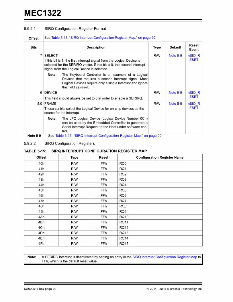
MEC1322
5.9.2.1 SIRQ Configuration Register Format
Note 5-9 See Table 5-15, “SIRQ Interrupt Configuration Register Map,” on page 90.
5.9.2.2 SIRQ Configuration Registers
Offset See Table 5-15, “SIRQ Interrupt Configuration Register Map,” on page 90.
Bits Description Type DefaultReset Event
7 SELECT
If this bit is 1, the first interrupt signal from the Logical Device is selected for the SERIRQ vector. If this bit is 0, the second interrupt signal from the Logical Device is selected.
Note: The Keyboard Controller is an example of a LogicalDevices that requires a second interrupt signal. MostLogical Devices require only a single interrupt and ignorethis field as result.
R/W Note 5-9 nSIO_RESET
6 DEVICE
This field should always be set to 0 in order to enable a SERIRQ.
R/W Note 5-9 nSIO_RESET
5:0 FRAME
These six bits select the Logical Device for on-chip devices as the source for the interrupt.
Note: The LPC Logical Device (Logical Device Number 0Ch)can be used by the Embedded Controller to generate aSerial Interrupt Request to the Host under software con-trol.
R/W Note 5-9 nSIO_RESET
TABLE 5-15: SIRQ INTERRUPT CONFIGURATION REGISTER MAP
Offset Type Reset Configuration Register Name
40h R/W FFh IRQ0
41h R/W FFh IRQ1
42h R/W FFh IRQ2
43h R/W FFh IRQ3
44h R/W FFh IRQ4
45h R/W FFh IRQ5
46h R/W FFh IRQ6
47h R/W FFh IRQ7
48h R/W FFh IRQ8
49h R/W FFh IRQ9
4Ah R/W FFh IRQ10
4Bh R/W FFh IRQ11
4Ch R/W FFh IRQ12
4Dh R/W FFh IRQ13
4Eh R/W FFh IRQ14
4Fh R/W FFh IRQ15
Note: A SERIRQ interrupt is deactivated by setting an entry in the SIRQ Interrupt Configuration Register Map toFFh, which is the default reset value.
DS00001719D-page 90 2014 - 2015 Microchip Technology Inc.
MEC1322
5.9.3 I/O BASE ADDRESS REGISTERS (BARS)
The LPC Controller has implemented a Base Address Register (BAR) for each Logical Device in the LPC Configurationspace.
• For a description of the Base Address Register format see Section 5.9.3.1, "I/O Base Address Register Format," on page 91.
• For a description of the BARs per Logical Device see Table 5-16, “I/O Base Address Registers,” on page 92.
On every LPC bus I/O access the unmasked portion of the programmed LPC Host Address in each of the Base AddressRegisters are checked in parallel and if any matches the LPC I/O address the LPC Controller claims the bus cycle.
The format of each BAR is summarized in Section 5.9.3.1, "I/O Base Address Register Format," on page 91.
5.9.3.1 I/O Base Address Register Format
Each LPC accessible logical device has a programmable Base Address Register. The following table defines thegeneric format used for all of these registers. See Table 5-16, "I/O Base Address Registers" for a list of all the LogicalDevice Base Address registers implemented.
Note 5-10 Offset 60h is the LPC Base Address register. The LPC Base Address register is only reset onVCC1_RESET. However, bits[31:16] are reloaded on nSIO_RESET with the value in the LPC BARInit Register.
Note 5-11 Bits[31:16] LPC Host Address bit field in the LPC Base Address register at offset 60h must be writtenLSB then MSB. This particular register has a shadow that lets the Host come in and write to the lowerbyte of the 16-bit address, and the resulting 16-bit LPC Host address field does not update. Writingto the upper byte triggers a full 16-bit field update.
Note: Software should that insure that no two BARs map the same LPC I/O address. If two BARs do map to thesame address, the LPC_INTERNAL_ERR and BAR_CONFLICT status bits are set when an LPC accessis targeting the address with the BAR conflict.
Offset See Table 5-16, “I/O Base Address Registers,” on page 92
Bits Description Type DefaultReset Event
31:16 LPC Host Address
These 16 bits are used to match LPC I/O addresses
R/W(Note 5-
11)
See Table 5-16
Note 5-10
15 VALID
If this bit is 1, the BAR is valid and will participate in LPC matches. If it is 0 this BAR is ignored
R/W See Table 5-16
Note 5-10
14 DEVICE (device)
This bit combined with FRAME constitute the Logical Device Num-ber. DEVICE identifies the physical location of the logical device. This bit should always be set to 0.
R See Table 5-16
Note 5-10
13:8 FRAME
These 6 bits are used to specify a logical device frame number within a bus. This field is multiplied by 400h to provide the frame address within the peripheral bus address. Frame values for frames corresponding to logical devices that are not present on the device are invalid.
R See Table 5-16
Note 5-10
7:0 MASK
These 8 bits are used to mask off address bits in the address match between an LPC I/O address and the Host Address field of the BARs, as described in Section 5.8.2.1, "I/O Transactions". A block of up to 256 8-bit registers can be assigned to one base address.
R See Table 5-16
Note 5-10
2014 - 2015 Microchip Technology Inc. DS00001719D-page 91

MEC1322
5.9.3.2 Logical Device I/O BAR Description
The following table defines the LPC I/O BAR of each logical device implemented in the design.
TABLE 5-16: I/O BASE ADDRESS REGISTERS
5.9.4 DEVICE MEMORY BASE ADDRESS REGISTERS
Some Logical Devices have a Memory Base Address Register. These Device Memory BARs are located in blocks ofConfiguration Registers in Logical Device 0Ch, in the AHB address range 400F_33C0h through 400F_33FFh. The fol-lowing table defines the generic format used for all of these registers.
Each Device Memory BAR is 48 bits wide. The format of each Device Memory BAR is summarized in Device MemoryBase Address Register Format. An LPC memory request is translated by the Device Memory BAR into an 8-bit read orwrite transaction on the AHB bus. The 32-bit LPC memory address is translated into a 24-bit AHB address
5.9.4.1 Device Memory Base Address Register Format
Offset See Table 5-17, "Device Memory Base Address Register Default Values"
Bits Description Type DefaultReset Event
47:16 HOST_ADDRESS[31:0]These 32 bits are used to match LPC memory addresses.
R/W See Table 5-17
nSIO_RESET
15 VALIDIf this bit is 1, the BAR is valid and will participate in LPC matches. If it is 0 this BAR is ignored.
R/W See Table 5-17
nSIO_RESET
14 RESERVED RES - -
Bits [D31:D16] Bit [D15] Bit [D14]
Bits [D13:D8]
Bits [D6:D0]
Offset
Logical Device
Number Logical Devices Reset Default
Default LPC I/O
Host Address VALID DEVICE FRAME MASK
60h CLPC Interface
(Configuration Port)002E_0C01
(Note 1) 002E 0 0 C 1
64h 0 EMI 0 0000_000F 0000 0 0 0 F68h 7 UART 0 0000_0707 0000 0 0 7 778h 1 8042EM 0060_0104 0060 0 0 1 488h 3 ACPI EC0 0062_0304 0062 0 0 3 48Ch 4 ACPI EC1 0066_0407 0066 0 0 4 790h 5 ACPI PM1 0000_0507 0000 0 0 5 794h 6 Legacy Port92/GateA20 0092_0600 0092 0 0 6 098h 9 Mailbox 0000_0901 0000 0 0 9 19Ch B RTC 0000_0B3F 0000 0 0 B 3F
Base Address Register Bit Field Descriptions
Note 2: The FRAME and MASK fields for these Legacy devices are not used to determine which LPC I/O addresses to claim. The address range match is maintained within the blocks themselves.
Note 1: The default Base I/O Address of the Configuration Port can be relocated by programming the BAR register for Logical Device Ch (LPC/Configuration Port) at offset 60h.
DS00001719D-page 92 2014 - 2015 Microchip Technology Inc.

MEC1322
Note 5-12 The Mask and Frame fields of all logical devices are read-only except for 3h (ACPI EC Channel 0).
5.9.4.2 Device Memory Base Address Register Table
Table 5-17 lists the Base Address Registers for logical devices which have LPC memory access in the MEC1322.
LPC Memory cycle access is controlled by LPC Memory Base Address Registers. LPC Memory BAR registers arelocated in LDN Ch (LPC Interface) at AHB base address 400F_3300h starting at the offset shown in Table 5-17.
Note 1: The VALID, DEVICE, FRAME and MASK fields are as shown in Table 5-16, "I/O Base Address Registers".
5.10 Runtime Registers
The runtime registers listed in Table 5-19, "Runtime Register Summary" are for a single instance of the LPC Interface.The addresses of each register listed in Table 5-19 are defined as a relative offset to the host “Begin Address” define inTable 5-2.
Note 1: The Begin Address indicates where the first register can be accessed in a particular address space for ablock instance.
2: The LPC Runtime registers are only accessible from the LPC interface and are used to implement the LPCConfiguration Port. They are not accessible by any other Host.
13:8 FRAMEThese 6 bits are used to specify a logical device frame number within a bus. This field is multiplied by 400h to provide the frame address within the peripheral bus address. In the MEC1322 Frame values for frames corresponding to logical devices that are not present on the MEC1322 are invalid.
Note 5-12
See Table 5-17
nSIO_RESET
7:0 MASKThese bits are used to mask off address bits in the address match between an LPC memory address and the Host Address field of the BARs, as described in the following section.
Note 5-12
See Table 5-17
nSIO_RESET
TABLE 5-17: DEVICE MEMORY BASE ADDRESS REGISTER DEFAULT VALUES
LPC offset in CR space
Logical Device Number
Logical DeviceMemory BAR Default
ValueLPC Memory Address
C0h 9h Mailbox 0000_0000_0901h 0000_0000h
C6h 3h ACPIEC0 0000_0062_0304h 0000_0062h
CCh 4h ACPIEC1 0000_0066_0407h 0000_0066h
D2h 0h EMI 0000_0000_000Fh 0000_0000h
TABLE 5-18: RUNTIME REGISTER ADDRESS RANGE TABLE
INSTANCE NAMEINSTANCE NUMBER HOST
ADDRESS SPACE BEGIN ADDRESS
LPC Interface0 LPC LPC I/O Base I/O Address of
Logical Device Ch +00h
Offset See Table 5-17, "Device Memory Base Address Register Default Values"
Bits Description Type DefaultReset Event
2014 - 2015 Microchip Technology Inc. DS00001719D-page 93

MEC1322
5.10.1 INDEX REGISTER
5.10.2 DATA REGISTER
5.11 EC-Only Registers
The registers listed in Table 5-21, "EC-Only Register Summary" are for a single instance of the LPC Interface. Theiraddresses are defined as a relative offset to the host base address defined in Table 5-20.
The following table defines the fixed host base address for each LPC Interface instance.
The Begin Address indicates where the first register can be accessed in a particular address space for a block instance.
TABLE 5-19: RUNTIME REGISTER SUMMARY
Offset Register Name
00h INDEX Register
01h DATA Register
Note: The LPC Runtime Register space has been used to implement the INDEX and DATA registers in the Con-figuration Port. In CONFIG_MODE, the Configuration Port is used to access the Configuration Registers.
Offset 00h
Bits Description Type DefaultReset Event
7:0 INDEX
The INDEX register, which is part of the Configuration Port, is used as a pointer to a Configuration Register Address.
Note: For a description of accessing the Configuration Port seeSection 5.8.3, "Configuration Port," on page 83.
R/W 0h VCC1_RESET
Offset 01h
Bits Description Type DefaultReset Event
7:0 DATA
The DATA register, which is part of the Configuration Port, is used to read or write data to the register currently being selected by the INDEX Register.
Note: For a description of accessing the Configuration Port seeSection 5.8.3, "Configuration Port," on page 83
R/W 0h VCC1_RESET
Note: EC-Only registers are not accessible by the LPC interface.
TABLE 5-20: EC-ONLY REGISTER ADDRESS RANGE TABLE
INSTANCE NAMEINSTANCE NUMBER HOST
ADDRESS SPACE BEGIN ADDRESS
LPC Interface 0 EC 32-bit internal address space
400F_3100h
DS00001719D-page 94 2014 - 2015 Microchip Technology Inc.

MEC1322
5.11.1 LPC BUS MONITOR REGISTER
5.11.2 HOST BUS ERROR REGISTER
TABLE 5-21: EC-ONLY REGISTER SUMMARY
Offset Register Name
04h LPC Bus Monitor Register
08h Host Bus Error Register
0Ch EC SERIRQ Register
10h EC Clock Control Register
14h MCHP Test Register
18h MCHP Test Register
20h BAR Inhibit Register
24h MCHP Reserved
28h MCHP Reserved
2Ch MCHP Reserved
30h LPC BAR Init Register
Note: MCHP Reserved registers are read/write registers. Modifying these registers may have unwanted results.
Offset 04h
Bits Description Type DefaultReset Event
31:2 RESERVED RES - -
1 LRESET_STATUS
This bit reflects the state of the LRESET# input pin. The LRE-SET_Status is the inverse of the LRESET# pin.
When the LRESET_Status bit is ‘0b’, the LRESET# input pin is de-asserted (that is, the pin has the value ‘1b’). When the LRESET_Sta-tus bit is ‘1b’, the LRESET# input pin is asserted (that is, the pin has the value ‘0b’).
R 0h VCC1_RESET
0 MCHP Reserved R 0h VCC1_RESET
Offset 08h
Bits Description Type DefaultReset Event
31:8 ErrorAddress[23:16]
This 24-bit field captures the 24-bit internal address of every LPC transaction whenever the bit LPC_INTERNAL_ERR in this register is 0. When LPC_INTERNAL_ERR is 1 this register is not updated but retains its previous value. When bus errors occur this field saves the address of the first address that caused an error.
R 0h VCC1_RESET
5 DMA_ERR
This bit is set to 1 whenever EN_INTERNAL_ERR is 1 and an LPC DMA access causes an internal bus error. Once set, it remains set until cleared by being written with a 1.
R/WC 0h VCC1_RESET
2014 - 2015 Microchip Technology Inc. DS00001719D-page 95

MEC1322
5.11.3 EC SERIRQ REGISTER
5.11.4 EC CLOCK CONTROL REGISTER
4 CONFIG_ERR
This bit is set to 1 whenever EN_INTERNAL_ERR is 1 and an LPC Configuration access causes an internal bus error. Once set, it remains set until cleared by being written with a 1.
R/WC 0h VCC1_RESET
3 RUNTIME_ERR
This bit is set to 1 whenever EN_INTERNAL_ERR is 1 and an LPC I/O access causes an internal bus error. This error will only occur if a BAR is misconfigured. Once set, it remains set until cleared by being written with a 1.
R/WC 0h VCC1_RESET
2 BAR_CONFLICT
This bit is set to 1 whenever a BAR conflict occurs on an LPC address. A Bar conflict occurs when more than one BAR matches the address during of an LPC cycle access. Once this bit is set, it remains set until cleared by being written with a 1.
R/WC 0h VCC1_RESET
1 EN_INTERNAL_ERR
When this bit is 0, only a BAR conflict, which occurs when two BARs match the same LPC I/O address, will cause LPC_INTERNAL_ERR to be set. When this bit is 1, internal bus errors will also cause LPC_INTERNAL_ERR to be set.
R/WC 0h VCC1_RESET
0 LPC_INTERNAL_ERR
This bit is set whenever a BAR conflict or an internal bus error occurs as a result of an LPC access. Once set, it remains set until cleared by being written with a 1. This signal may be used to gener-ate interrupts. See Section 5.6, "Interrupts," on page 78.
R/WC 0h VCC1_RESET
Offset 0Ch
Bits Description Type DefaultReset Event
31:1 RESERVED RES - -
0 EC_IRQ
If the LPC Logical Device is selected as the source for a Serial Inter-rupt Request by an Interrupt Configuration register (see Section 5.8.4.8, "SERIRQ Interrupts," on page 87), this bit is used as the interrupt source.
R/W 0h VCC1_RESET
Offset 10h
Bits Description Type DefaultReset Event
31:3 RESERVED RES - -
2 Handshake
This bit controls throughput of LPC transactions.When this bit is a ‘0’ the part supports a 33MHz PCI Clock. When this bit is a ‘1’, the part supports a PCI Clock from 19.2MHz (includ-ing 24MHz) to 33MHz.
RES 1h VCC1_RESET
Offset 08h
Bits Description Type DefaultReset Event
DS00001719D-page 96 2014 - 2015 Microchip Technology Inc.

MEC1322
5.11.5 MCHP TEST REGISTER
5.11.6 MCHP TEST REGISTER
1:0 Clock_Control
This field controls when the host interface will permit the internal ring oscillator to be shut down. The choices are as follows:0h: Reserved1h: The host interface will permit the internal clocks to be shut down if the CLKRUN# signals “CLOCK STOP” and there are no pending serial interrupt request or DMA requests from devices associated with the device. The CLKRUN# signals “CLOCK STOP” by CLKRUN# being high for 5 LPCCLK’s after the raising edge of CLKRUN#2h: The host interface will permit the ring oscillator to be shut down after the completion of every LPC transaction. This mode may cause an increase in the time to respond to LPC transactions if the ring oscillator is off when the LPC transaction is detected.3h: The ring oscillator is not permitted to shut down as long as the host interface is active. When the ACTIVATE bit in the LPC Activate Register is 0, the Host Interface will permit the ring oscillator to be shut down and the Clock_Control Field is ignored. The Clock_Con-trol Field only effects the Host Interface when the ACTIVATE bit in the LPC Activate Register is 1.
Although the Host Interface can permit the internal oscillator to shut down, it cannot turn the oscillator on in response to an LPC transac-tion that occurs while the oscillator is off. In order to restart the oscil-lator in order to complete an LPC transaction, EC firmware must enable a wake interrupt on the LPC LFRAME# input. See the Appli-cation Note in Section 15.8.1, "WAKE Generation" for details.
R/W 0h VCC1_RESET
Offset 14h
Bits Description Type DefaultReset Event
31:8 RESERVED RES - -
7:0 MCHP Reserved R 0h VCC1_RESET
Offset 18h
Bits Description Type DefaultReset Event
31:2 RESERVED RES - -
1 MCHP Reserved R/W 0h VCC1_RESET
0 MCHP Reserved R/W 0h VCC1_RESET
Offset 10h
Bits Description Type DefaultReset Event
2014 - 2015 Microchip Technology Inc. DS00001719D-page 97
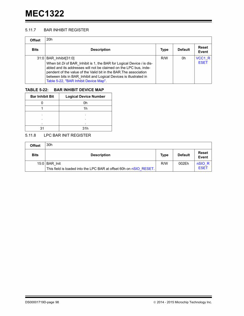
MEC1322
5.11.7 BAR INHIBIT REGISTER
5.11.8 LPC BAR INIT REGISTER
Offset 20h
Bits Description Type DefaultReset Event
31:0 BAR_Inhibit[31:0]
When bit Di of BAR_Inhibit is 1, the BAR for Logical Device i is dis-abled and its addresses will not be claimed on the LPC bus, inde-pendent of the value of the Valid bit in the BAR.The association between bits in BAR_Inhibit and Logical Devices is illustrated in Table 5-22, "BAR Inhibit Device Map".
R/W 0h VCC1_RESET
TABLE 5-22: BAR INHIBIT DEVICE MAP
Bar Inhibit Bit Logical Device Number
0 0h
1 1h
.
.
.
.
.
.
31 31h
Offset 30h
Bits Description Type DefaultReset Event
15:0 BAR_Init
This field is loaded into the LPC BAR at offset 60h on nSIO_RESET.
R/W 002Eh nSIO_RESET
DS00001719D-page 98 2014 - 2015 Microchip Technology Inc.

MEC1322
6.0 CHIP CONFIGURATION
6.1 Introduction
This chapter defines the mechanism to configure the device.
6.2 Terminology
This section documents terms used locally in this chapter. Common terminology that is used in the chip specification iscaptured in the Chip-Level Terminology section.
6.3 Interface
This block is designed to be accessed via the Host accessible Configuration Port.
TABLE 6-1: TERMINOLOGY
Term Definition
Global Configuration Registers Registers used to configure the chip that are always accessible via the Configuration Port
Logical Device Configuration Registers Registers used to configure a logical device in the chip. These registers are only accessible via the Configuration Port when enabled via the Global Configuration registers.
FIGURE 6-1: BLOCK DIAGRAM OF CONFIGURATION PORT00
h – 2
Fh
30h
– F
Fh
Logical Device Configuration Registers
Chip-LevelGlobal Configuration Registers
Logical D
evices[0
:n]
Configuration Port
2014 - 2015 Microchip Technology Inc. DS00001719D-page 99

MEC1322
6.3.1 HOST INTERFACE
The registers defined for the Chip Configuration are accessible by the Configuration Port when the device is in CONFIGMODE. For a description of the Configuration Port and CONFIG MODE see the description of the LPC Interface.
6.4 Power, Clocks and Reset
This section defines the Power, Clock, and Reset input parameters to this block.
6.4.1 POWER DOMAINS
6.4.2 CLOCK INPUTS
This block does not require any special clock inputs.
6.4.3 RESETS
6.5 Interrupts
This block does not generate any interrupts.
6.6 Low Power Modes
This block always automatically adjusts to operate in the lowest power mode.
6.7 Description
The Chip Configuration Registers are divided into two groups: Global Configuration Registers and Logical Device Con-figuration registers. The following descriptions assume that the LPC interface has already been configured to operatein CONFIG MODE.
• Global Configuration Registers are always accessible via the LPC Configuration Port.
• The Logical Device Configuration registers are only accessible via the LPC Configuration Port when the corre-sponding Logical Device Number is loaded in the Logical Device Number register. The Logical Device Number register is a Global Configuration Register.
There are 48 8-bit Global Configuration Registers (at offsets 00h through 2Fh), plus up to 208 8-bit registers associatedwith each Logical Device. The Logical Device is selected with the Logical Device Number Register (Global ConfigurationRegister 07h).
Sequence to Access Logical Device Configuration Register:
a) Write the number of the Logical Device being accessed in the Logical Device Number Configuration Register bywriting 07h into the INDEX PORT and the Logical Device Number into the DATA PORT.
b) Write the address of the desired logical device configuration register to the INDEX PORT and then write or readthe value of the configuration register through the DATA PORT.
Note: Each logical device has a bank of Configuration registers that are accessible at offsets 30h to FFh via theConfiguration Port. The Logical Device number programmed in offset 07h determines which bank of con-figuration registers is currently accessible.
TABLE 6-2: POWER SOURCES
Name Description
VCC1 The logic and registers implemented in this block reside on this singlepower well.
TABLE 6-3: RESET SIGNALS
Name Description
VCC1_RESET Power on Reset to the block. This signal resets all the register and logic in this block to its default state.
DS00001719D-page 100 2014 - 2015 Microchip Technology Inc.

MEC1322
Note 1: If accessing the Global Configuration Registers, step (a) is not required.
2: Any write to an undefined or reserved Configuration register is terminated normally on the LPC bus withoutany modification of state in the MEC1322. Any read to an undefined or reserved Configuration registerreturns FFh.
The following sections define the Global Configuration registers and the Logical Configuration registers.
6.7.1 GLOBAL CONTROL/CONFIGURATION REGISTERS
As with all Configuration Registers, the INDEX PORT is used to select a Global Configuration Register in the chip. TheDATA PORT is then used to access the selected register. The INDEX and DATA PORTs are defined in the LPC Interfacedescription.
The Host can access all the Global Configuration registers at the offsets listed in Table 6-4, "Chip-Level (Global) Con-trol/Configuration Registers" through the INDEX PORT and the DATA PORT.
The EC can access all the Global Configuration registers at the offsets listed in Table 6-4, "Chip-Level (Global) Con-trol/Configuration Registers" from the base address shown in Table 6-6, “EC-Only Register Address Table,” onpage 102.
6.7.2 LOGICAL DEVICE CONFIGURATION REGISTERS
The Logical Device Configuration registers support motherboard designs in which the resources required by their com-ponents are known and assigned by the BIOS at POST.
Each logical device may have a set of directly I/O addressable Runtime Registers, Configuration Registers accessiblevia the Configuration Port, or DMA registers. The following table lists the register types for each LPC Host-accessibleLogical Device implemented in the design. The Embedded Controller (EC) can access all Configuration Registers andall Runtime Registers directly.
TABLE 6-4: CHIP-LEVEL (GLOBAL) CONTROL/CONFIGURATION REGISTERS
Register Offset Description
Chip (Global) Control Registers
Reserved 00h - 06h Reserved - Writes are ignored, reads return 0.
Logical Device Number 07h A write to this register selects the current logical device. This allows access to the control and configuration registers for each logical device.
Note: The Activate command operates only on theselected logical device.
Reserved 08h - 1Fh Reserved - Writes are ignored, reads return 0.
Device ID 20h A read-only register which provides device identification:Bits[7:0] = 15h
Device RevisionHard Wired
21h A read-only register which provides device revision information.
Bits[7:0] = current revision when read
Reserved 24h Reserved – writes are ignored, reads return “0”.
MCHP Reserved 25h - 2Fh MCHP Reserved. This register locations are reserved for Microchip use. Modify-ing these locations may cause unwanted results.
2014 - 2015 Microchip Technology Inc. DS00001719D-page 101

MEC1322
TABLE 6-5: HOST LOGICAL DEVICES ON MEC1322
6.8 EC-Only Registers
Note 6-1 The Base Address indicates where the first register can be accessed in a particular address spacefor a block instance.
The chip-level (global) registers reside in Logical Device 3Fh at EC addresses 400F_FF00h through 400F_FF2Fh.
The EC can access all these registers at the addresses listed in Table 6-4, “Chip-Level (Global) Control/ConfigurationRegisters,” on page 101.
TABLE 6-6: EC-ONLY REGISTER ADDRESS TABLE
Block InstanceInstance Number
Host Address Space Base Address (Note 6-1)
HOST_REGS 0 EC 32-bit internal address space
400F_FF00h
Logica l Device
Num ber Logica l Devices
LPC I/O Runtim e Access
LPC I/O Configura tion
Access
0 EMI 0 yes no1 8042EM no yes3 ACPI EC0 yes no4 ACPI EC1 yes no5 ACPI PM1 yes no6 Legacy Port92/GateA20 yes yes7 UART 0 yes yes9 Mailbox yes noB RTC yes no
DS00001719D-page 102 2014 - 2015 Microchip Technology Inc.

MEC1322
7.0 ARM M4F BASED EMBEDDED CONTROLLER
7.1 Introduction
This chapter contains a description of the ARM M4F Embedded Controller (EC).
The EC is built around an ARM® Cortex®-M4F Processor provided by Arm Ltd. (the “ARM M4F IP”). The ARM Cortex®M4F is a full-featured 32-bit embedded processor, implementing the ARMv7-M THUMB instruction set and FPU instruc-tion set in hardware.
The ARM M4F IP is configured as a Von Neumann, Byte-Addressable, Little-Endian architecture. It provides a singleunified 32-bit byte-level address, for a total direct addressing space of 4GByte. It has multiple bus interfaces, but theseexpress priorities of access to the chip-level resources (Instruction Fetch vs. Data RAM vs. others), and they do notrepresent separate addressing spaces.
The ARM M4F IP has configurable options, which are selected as follows.
• Little-Endian byte ordering is selected at all times (hard-wired)
• Bit Banding feature is included for efficient bit-level access.
• Floating-Point Unit (FPU) is included, to implement the Floating-Point instruction set in hardware
• Debug features are included at “Ex+” level, defined as follows:
• DWT Unit provides 4 Data Watchpoint comparators and Execution Monitoring
• FPB Unit provides HW Breakpointing with 6 Instruction and 2 Literal (Read-Only Data) address comparators. The FPB comparators are also available for Patching: remapping Instruction and Literal Data addresses.
• Trace features are included at “Full” level, defined as follows:
• DWT for reporting breakpoints and watchpoints
• ITM for profiling and to timestamp and output messages from instrumented firmware builds
• ETM for instruction tracing, and for enhanced reporting of Core and DWT events
• The ARM-defined HTM trace feature is not currently included.
• NVIC Interrupt controller with 8 priority levels and up to 240 individually-vectored interrupt inputs.
• A Microchip-defined Interrupt Aggregator function (at chip level) may be used to group multiple interrupts onto sin-gle NVIC inputs.
• The ARM-defined WIC feature is not currently included.
• Microchip Interrupt Aggregator function (at chip level) is expected to provide Wake control instead.
• The ARM-defined MPU feature is not currently included.
• Memory Protection functionality is not expected to be necessary.
7.2 References
• ARM Limited: Cortex®-M4 Technical Reference Manual, DDI0439C, 29 June 2010
• ARM Limited: ARM®v7-M Architecture Reference Manual, DDI0403D, November 2010
• NOTE: Filename DDI0403D_arm_architecture_v7m_reference_manual_errata_markup_1_0.pdf
• ARM® Generic Interrupt Controller Architecture version 1.0 Architecture Specification, IHI0048A, September 2008
• ARM Limited: AMBA® Specification (Rev 2.0), IHI0011A, 13 May 1999
• ARM Limited: AMBA® 3 AHB-Lite Protocol Specification, IHI0033A, 6 June 2006
• ARM Limited: AMBA® 3 ATB Protocol Specification, IHI0032A, 19 June 2006
• ARM Limited: Cortex-M™ System Design Kit Technical Reference Manual, DDI0479B, 16 June 2011
• ARM Limited: CoreSight™ v1.0 Architecture Specification, IHI0029B, 24 March 2005
• ARM Limited: CoreSight™ Components Technical Reference Manual, DDI0314H, 10 July 2009
• ARM Limited: ARM® Debug Interface v5 Architecture Specification, IHI0031A, 8 February 2006
• ARM Limited: ARM® Debug Interface v5 Architecture Specification ADIv5.1 Supplement, DSA09-PRDC-008772, 17 August 2009
• ARM Limited: Embedded Trace Macrocell™ (ETMv1.0 to ETMv3.5) Architecture Specification, IHI0014Q, 23 Sep-tember 2011
• ARM Limited: CoreSight™ ETM™-M4 Technical Reference Manual, DDI0440C, 29 June 2010
2014 - 2015 Microchip Technology Inc. DS00001719D-page 103
MEC1322
7.3 Terminology
7.3.1 ARM IP TERMS AND ACRONYMS
• Cortex-M4F
• The ARM designation for the specific IP selected for this product: a Cortex M4 processor core containing a hard-ware Floating Point Unit (FPU).
• ARMv7
• The identifying name for the general architecture implemented by the Cortex-M family of IP products.
• Note that ARMv7 has no relationship to the older “ARM 7” product line, which is classified as an “ARMv3” archi-tecture, and is very different.
• FPU
• Floating-Point Unit: a subblock included in the Core for implementing the Floating Point instruction set in hard-ware.
• NVIC
• Nested Vectored Interrupt Controller subblock. Accepts external interrupt inputs. See documents ARM Limited: ARM®v7-M Architecture Reference Manual, DDI0403D, November 2010 and ARM® Generic Interrupt Controller Architecture version 1.0 Architecture Specification, IHI0048A, September 2008.
• FPB
• FLASH Patch Breakpoint subblock. Provides either Remapping (Address substitution) or Breakpointing (Excep-tion or Halt) for a set of Instruction addresses and Data addresses. See Section 8.3 of ARM Limited: Cortex®-M4 Technical Reference Manual, DDI0439C, 29 June 2010.
• DAP
• Debug Access Port, a subblock consisting of DP and AP subblocks
• DP
• Any of the ports in the DAP subblock for connection to an off-chip Debugger. A single SWJ-DP option is currently selected for this function, providing JTAG connectivity.
• SWJ-DP
• Serial Wire / JTAG Debug Port, the DP option selected by Microchip for the DAP.
• AP
• Any of the ports on the DAP subblock for accessing on-chip resources on behalf of the Debugger, independent of processor operations. A single AHB-AP option is currently selected for this function.
• AHB-AP
• AHB Access Port, the AP option selected by Microchip for the DAP.
• MEM-AP
• A generic term for an AP that connects to a memory-mapped bus on-chip. For this product, this term is synony-mous with the AHB Access Port, AHB-AP.
• ROM Table
• A ROM-based data structure in the Debug section that allows an external Debugger and/or a FW monitor to deter-mine which of the Debug features are present.
• DWT
• Data Watchdog and Trace subblock. This contains comparators and counters used for data watchpoints and Core activity tracing.
• ETM
• Embedded Trace Macrocell subblock. Provides enhancements for Trace output reporting, mostly from the DWT subblock. It adds enhanced instruction tracing, filtering, triggering and timestamping.
• ITM
• Instrumentation Trace Macrocell subblock. Provides a HW Trace interface for “printf”-style reports from instru-mented firmware builds, with timestamping also provided.
• TPIU
• Trace Port Interface Unit subblock. Multiplexes and buffers Trace reports from the ETM and ITM subblocks.
• TPA
• Trace Port Analyzer: any off-chip device that uses the TPIU output.
• ATB
DS00001719D-page 104 2014 - 2015 Microchip Technology Inc.

MEC1322
• Interface standard for Trace data to the TPIU from ETM and/or ITM blocks, Defined in AMBA 3. See ARM Limited: AMBA® 3 ATB Protocol Specification, IHI0032A, 19 June 2006.
• AMBA
• The collective term for bus standards originated by ARM Limited.
• AMBA 3 defines the IP’s AHB-Lite and ATB bus interfaces.
• AMBA 2 (AMBA Rev. 2.0) defines the EC’s AHB bus interface.
• AHB
• Advanced High-Performance Bus, a system-level on-chip AMBA 2 bus standard. See ARM Limited: AMBA® Specification (Rev 2.0), IHI0011A, 13 May 1999.
• AHB-Lite
• A Single-Master subset of the AHB bus standard: defined in the AMBA 3 bus standard. See ARM Limited: AMBA® 3 AHB-Lite Protocol Specification, IHI0033A, 6 June 2006.
• PPB
• Private Peripheral Bus: A specific APB bus with local connectivity within the EC.
• APB
• Advanced Peripheral Bus, a limited 32-bit-only bus defined in AMBA 2 for I/O register accesses. This term is rele-vant only to describe the PPB bus internal to the EC core. See ARM Limited: AMBA® Specification (Rev 2.0), IHI0011A, 13 May 1999.
• MPU
• Memory Protection Unit. This is an optional subblock that is not currently included.
• HTM
• AHB Trace Macrocell. This is an optional subblock that is not currently included.
• WIC
• Wake-Up Interrupt Controller. This is an optional subblock that is not currently included.
7.3.2 MICROCHIP TERMS AND ACRONYMS
• PMU
• This Processor Memory Unit is a module that may be present at the chip level containing any memory resources that are closely-coupled to the MEC1322 EC. It manages accesses from both the EC processor and chip-level bus masters.
• Interrupt Aggregator
• This is a module that may be present at the chip level, which can combine multiple interrupt sources onto single interrupt inputs at the EC, causing them to share a vector.
7.4 ARM M4F IP Interfaces
This section defines only the interfaces to the ARM IP itself. For the interfaces of the entire block, see Section 7.5, "BlockExternal Interfaces," on page 107.
The MEC1322 IP has the following major external interfaces, as shown in FIGURE 7-1: ARM M4F Based EmbeddedController I/O Block Diagram on page 107:
• ICode AHB-Lite Interface
• DCode AHB-Lite Interface
• System AHB-Lite Interface
• Debug (JTAG) Interface
• Trace Port Interface
• Interrupt Interface
The EC operates on the model of a single 32-bit addressing space of byte addresses (4Gbytes, Von Neumann archi-tecture) with Little-Endian byte ordering. On the basis of an internal decoder (part of the Bus Matrix shown in Figure 7-1), it routes Read/Write/Fetch accesses to one of three external interfaces, or in some cases internally (shown as thePPB interface).
2014 - 2015 Microchip Technology Inc. DS00001719D-page 105

MEC1322
The EC executes instructions out of closely-coupled memory via the ICode Interface. Data accesses to closely-coupledmemory are handled via the DCode Interface. The EC accesses the rest of the on-chip address space via the SystemAHB-Lite interface. The Debugger program in the host can probe the EC and all EC addressable memory via the JTAGdebug interface.
Aliased addressing spaces are provided at the chip level so that specific bus interfaces can be selected explicitly whereneeded. For example, the EC’s Bit Banding feature uses the System AHB-Lite bus to access resources normallyaccessed via the DCode or ICode interface.
DS00001719D-page 106 2014 - 2015 Microchip Technology Inc.

MEC1322
7.5 Block External Interfaces
FIGURE 7-1: ARM M4F BASED EMBEDDED CONTROLLER I/O BLOCK DIAGRAM
ICodeInterface
(AHB-Lite)
DCodeInterface
(AHB-Lite)
System Interface
(AHB-Lite)
NVICNested
Vectored Interrupt
Controller
TPIUTrace Port Interface
ARM_M4F IP
Chip-Level System Bus
(AMBA 2 AHB)
Processor Core w/ FPU
Misc. Sideband
DAP Debug Access Port Mux
Chip-level JTAG TAP
ETM / ITM Trace Outputs
Debug Host
AMBA 2AHB Adapt
Memory Bus Adapt
Memory Bus Adapt
PMC Block(RAM / ROM)
Data Port
Code Port
AHB Port
ARM_M4F EC Block
Inte
rrup
t A
ggre
gat
or
Grouped (Summary)Interrupts
Directly Vectored Connections
Inte
rrup
ts
OptionallyGrouped
Inputs
UnconditionallyGrouped Inputs
ProcessorClock
Divider
Chip-LevelClock
Pulse Sync & Stretch
ClockGate
Processor Reset
Core Reset (POR)
2014 - 2015 Microchip Technology Inc. DS00001719D-page 107

MEC1322
7.6 Power, Clocks and Reset
This section defines the Power, Clock, and Reset parameters of the block.
7.6.1 POWER DOMAINS
7.6.2 CLOCK INPUTS
7.6.2.1 Basic Clocking
The basic clocking comes from a free-running Clock signal provided from the chip level.
7.6.2.2 System Tick Clocking
The System Tick clocking is controlled by a signal from chip-level logic. It is the 48 MHz Ring Oscillator divided by thefollowing:
- ((Processor Clock Divide Value)x2)+1.
7.6.2.3 Debug JTAG Clocking
The Debug JTAG clocking comes from chip-level logic, which may multiplex or gate this clock. See Section 7.9.3,"Debugger Access Support," on page 111.
7.6.2.4 Trace Clocking
The Clock for the Trace interface is identical to the 48 MHz Ring Oscillator input.
7.6.3 RESETS
The reset interface from the chip level is given below.
7.7 Interrupts
The ARM M4F Based Embedded Controller is equipped with an Interrupt Interface to respond to interrupts. These inputsgo to the IP’s NVIC block after a small amount of hardware processing to ensure their detection at varying clock rates.See FIGURE 7-1: ARM M4F Based Embedded Controller I/O Block Diagram on page 107.
As shown in Figure 7-1, an Interrupt Aggregator block may exist at the chip level, to allow multiple related interrupts tobe grouped onto the same NVIC input, and so allowing them to be serviced using the same vector. This may allow thesame interrupt handler to be invoked for a group of related interrupt inputs. It may also be used to expand the total num-ber of interrupt inputs that can be serviced.
Connections to the chip-level system are given in Table 15-3, “Interrupt Event Aggregator Routing Summary,” onpage 195.
The NMI (Non-Maskable Interrupt) connection is tied off and not used.
TABLE 7-1: POWER SOURCES
Name Description
VCC1 The ARM M4F Based Embedded Controller is powered by VCC1.
TABLE 7-2: CLOCK INPUTS
Name Description
48 MHz Ring Oscillator The EC clock derived from the 48 MHz Ring Oscillator is the clock source to the ARM M4F Based Embedded Controller. Division of the clock rate is allowed, according to the Processor Clock Enable.
Note: The EC clock is controlled from the chip-level Power, Clocks,and Reset (PCR) circuitry. See Section 3.9.8, "ProcessorClock Control Register (PROC_CLK_CNTRL)," on page 61.
TABLE 7-3: RESET SIGNALS
Name Description
EC_PROC_ RESET The ARM M4F Based Embedded Controller is reset by EC_PROC_ RESET.
DS00001719D-page 108 2014 - 2015 Microchip Technology Inc.

MEC1322
7.7.1 NVIC INTERRUPT INTERFACE
The NVIC interrupt unit can be wired to up to 240 interrupt inputs from the chip level. The interrupts that are actuallyconnected from the chip level are defined in Table 15-3, “Interrupt Event Aggregator Routing Summary,” on page 195.
All NVIC interrupt inputs can be programmed as either pulse or level triggered. They can also be individually masked,and individually assigned to their own hardware-managed priority level.
7.7.2 NVIC RELATIONSHIP TO EXCEPTION VECTOR TABLE ENTRIES
The Vector Table consists of 4-byte entries, one per vector. Entry 0 is not a vector, but provides an initial Reset valuefor the Main Stack Pointer. Vectors start with the Reset vector, at Entry #1. Entries up through #15 are dedicated forinternal exceptions, and do not involve the NVIC.
NVIC entries in the Vector Table start with Entry #16, so that NVIC Interrupt #0 is at Entry #16, and all NVIC interruptnumbers are incremented by 16 before accessing the Vector Table.
The number of connections to the NVIC determines the necessary minimum size of the Vector Table, as shown below.It can extend as far as 256 entries (255 vectors, plus the non-vector entry #0).
A Vector entry is used to load the Program Counter (PC) and the EPSR.T bit. Since the Program Counter only expressescode addresses in units of two-byte Halfwords, bit[0] of the vector location is used to load the EPSR.T bit instead, select-ing THUMB mode for exception handling. Bit[0] must be ‘1’ in all vectors, otherwise a UsageFault exception will beposted (INVSTATE, unimplemented instruction set). If the Reset vector is at fault, the exception posted will be HardFaultinstead.
TABLE 7-4: EXCEPTION AND INTERRUPT VECTOR TABLE LAYOUT
Table EntryException Number
Exception
Special Entry for Reset Stack Pointer
0 (none) Holds Reset Value for the Main Stack Pointer. Not a Vector.
Core Internal Exception Vectors start here
1 1 Reset Vector (PC + EPSR.T bit)
2 2 NMI (Non-Maskable Interrupt) Vector
3 3 HardFault Vector
4 4 MemManage Vector
5 5 BusFault Vector
6 6 UsageFault Vector
7 (none) (Reserved by ARM Ltd.)
8 (none) (Reserved by ARM Ltd.)
9 (none) (Reserved by ARM Ltd.)
10 (none) (Reserved by ARM Ltd.)
11 11 SVCall Vector
12 12 Debug Monitor Vector
13 (none) (Reserved by ARM Ltd.)
14 14 PendSV Vector
15 15 SysTick Vector
NVIC Interrupt Vectors start here
16 16 NVIC Interrupt #0 Vector
.
.
.
.
.
.
.
.
.
n + 16 n + 16 NVIC Interrupt #n Vector
.
.
.
.
.
.
.
.
.
2014 - 2015 Microchip Technology Inc. DS00001719D-page 109

MEC1322
7.8 Low Power Modes
The ARM processor low power modes are handled through the Power, Clocks, and Resets registers, not directly throughthe ARM core registers. See Section 3.7, "Chip Power Management Features," on page 54.
The ARM processor can enter Sleep or Deep Sleep mode internally. This action will cause an output signal ClockRequired to be turned off, allowing clocks to be stopped from the chip level. However, Clock Required will still be heldactive, or set to active, unless all of the following conditions exist:
• No interrupt is pending.
• An input signal Sleep Enable from the chip level is active.
• The Debug JTAG port is inactive (reset or configured not present).
In addition, regardless of the above conditions, a chip-level input signal Force Halt may halt the processor and removeClock Required.
7.9 Description
7.9.1 BUS CONNECTIONS
There are three bus connections used from MEC1322 EC block, which are directly related to the IP bus ports. See FIG-URE 7-1: ARM M4F Based Embedded Controller I/O Block Diagram on page 107.
For the mapping of addresses at the chip level, see Chapter 2.0, "Block Overview," on page 45.
7.9.1.1 Closely Coupled Instruction Fetch Bus
As shown in Figure 7-1, the AHB-Lite ICode port from the IP is converted to a more conventional SRAM memory-stylebus and connected to the on-chip memory resources with routing priority appropriate to Instruction Fetches.
7.9.1.2 Closely Coupled Data Bus
As shown in Figure 7-1, the AHB-Lite DCode port from the IP is converted to a more conventional SRAM memory-stylebus and connected to the on-chip memory resources with routing priority appropriate to fast Data Read/Write accesses.
7.9.1.3 Chip-Level System Bus
As shown in Figure 7-1, the AHB-Lite System port from the IP is converted from AHB-Lite to fully arbitrated multi-mastercapability (the AMBA 2 defined AHB bus: see ARM Limited: AMBA® Specification (Rev 2.0), IHI0011A, 13 May 1999).Using this bus, all addressable on-chip resources are available. The multi-mastering capability supports the MicrochipDMA and EMI features if present, as well as the Bit-Banding feature of the IP itself.
As also shown in Figure 7-1, the Closely-Coupled memory resources are also available through this bus connectionusing aliased addresses. This is required in order to allow Bit Banding to be used in these regions, but it also allowsthem to be accessed by DMA and other bus masters at the chip level.
APPLICATION NOTE: Registers with properties such as Write-1-to-Clear (W1C), Read-to-Clear and FIFOs need tobe handled with appropriate care when being used with the bit band alias addressingscheme. Accessing such a register through a bit band alias address will cause the hardwareto perform a read-modify-write, and if a W1C-type bit is set, it will get cleared with such anaccess. For example, using a bit band access to the Interrupt Aggregator, including theInterrupt Enables and Block Interrupt Status to clear an IRQ will clear all active IRQs.
max + 16 max + 16 NVIC Interrupt #max Vector (Highest-numbered NVIC connection.)
.
.
.
.
.
.
. Table size may (but need not) extend further.
.
.
255 255 NVIC Interrupt #239 (Architectural Limit of Exception Table)
TABLE 7-4: EXCEPTION AND INTERRUPT VECTOR TABLE LAYOUT (CONTINUED)
Table EntryException Number
Exception
DS00001719D-page 110 2014 - 2015 Microchip Technology Inc.

MEC1322
7.9.2 INSTRUCTION PIPELINING
There are no special considerations except as defined by ARM documentation.
7.9.3 DEBUGGER ACCESS SUPPORT
An external Debugger accesses the chip through a JTAG standard interface. The debugger itself, however, is not anARM product, and its capabilities will depend on the third-party product selected for code development and debug.
As shown in FIGURE 7-1: ARM M4F Based Embedded Controller I/O Block Diagram on page 107, there may be otherresources at the chip level that share the JTAG port pins; for example chip-level Boundary Scan. See Section 1.4.4,"JTAG Interface," on page 15 for configuring the JTAG pins at the chip level for Debug purposes.
7.9.3.1 Debug and Access Ports (SWJ-DP and AHB-AP Subblocks)
These two subblocks work together to provide access to the chip for the Debugger using the Debug JTAG connection,as described in Chapter 4 of the ARM Limited: ARM® Debug Interface v5 Architecture Specification, IHI0031A, 8 Feb-ruary 2006.
7.9.4 BREAKPOINT, WATCHPOINT AND TRACE SUPPORT
See ARM Limited: ARM® Debug Interface v5 Architecture Specification, IHI0031A, 8 February 2006 and also ARM Lim-ited: ARM® Debug Interface v5 Architecture Specification ADIv5.1 Supplement, DSA09-PRDC-008772, 17 August2009. A summary of functionality follows.
Breakpoint and Watchpoint facilities can be programmed to do one of the following:
• Halt the processor. This means that the external Debugger will detect the event by periodically polling the state of the EC.
• Transfer control to an internal Debug Monitor firmware routine, by triggering the Debug Monitor exception (see Table 7-4, “Exception and Interrupt Vector Table Layout,” on page 109).
7.9.4.1 Instrumentation Support (ITM Subblock)
The Instrumentation Trace Macrocell (ITM) is for profiling software. This uses non-blocking register accesses, with afixed low-intrusion overhead, and can be added to a Real-Time Operating System (RTOS), application, or exceptionhandler. If necessary, product code can retain the register access instructions, avoiding probe effects.
7.9.4.2 HW Breakpoints and ROM Patching (FPB Subblock)
The Flash Patch and Breakpoint (FPB) block. This block can remap sections of ROM, typically Flash memory, to regionsof RAM, and can set breakpoints on code in ROM. This block can be used for debug, and to provide a code or datapatch to an application that requires field updates to a product in ROM.
7.9.4.3 Data Watchpoints and Trace (DWT Subblock)
The Debug Watchpoint and Trace (DWT) block provides watchpoint support, program counter sampling for performancemonitoring, and embedded trace trigger control.
7.9.4.4 Trace Interface (ETM and TPIU)
The Embedded Trace Macrocell (ETM) provides instruction tracing capability. For details of functionality and usage, seealso ARM Limited: Embedded Trace Macrocell™ (ETMv1.0 to ETMv3.5) Architecture Specification, IHI0014Q, 23 Sep-tember 2011 and ARM Limited: CoreSight™ ETM™-M4 Technical Reference Manual, DDI0440C, 29 June 2010.
The Trace Port Interface Unit (TPIU) provides the external interface for the ITM, DWT and ETM.
See Section 1.4.16, "Trace Debug Interface," on page 19 for configuring the Trace pins at the chip level for Trace output.
7.10 ARM Configuration
In order to function correctly, it is necessary to set the ARM Auxiliary Control Register (ACTLR), located at address 0xE-000E008, to 0x02. This sets bit[1], DISDEFWBUF, to 1. This must be done as soon as possible after Power On Reset,or register corruption may occur.
2014 - 2015 Microchip Technology Inc. DS00001719D-page 111

MEC1322
8.0 RAM AND ROM
SRAM
The 128KBytes SRAM (Code or Data) is allocated as follows:
• 96K Optimized for Code
• 32K Optimized for Data.
The distinction between “96KB optimized for instructions” and “32KB optimized for data” SRAMs: is as follows:The MEC1322 has two blocks of SRAM, one of 96KB and one of 32KB. Both can be used for either instructions or data. As long as the ARM fetches instructions from one SRAM and does loads and stores to the other, code and data accesses operate in parallel and there are no wait states. If on the same cycle the ARM fetches an instruction and does a load or a store to the same SRAM, either the code fetch will be delayed by one cycle or the data access will be delayed by one cycle. The 96KB SRAM is optimized for instructions, in that if the ARM accesses this SRAM for both instructions and data on the same cycle, the instruction fetch will complete in one cycle and the load/store will be delayed for one cycle. The 32KB SRAM is optimized for data, in that if the ARM accesses this SRAM for both instructions and data on the same cycle, the load/store will complete in once cycle and the instruction fetch will be delayed for one cycle. In both cases, the SRAM arbiter ensures that the arbitration loser will win on subsequent cycles and thus will not be locked out of the SRAM indefinitely. User applications, therefore, are free to allocate code and data anywhere in the 128KB SRAM address space, except that there will be an occasional small performance hit if both code and data are allocated in the same SRAM.
The application loader in the MEC1322 ROM requires the top 8KB of the 32KB SRAM in order to perform its functions. The user can therefore load a maximum of 120KB into SRAM using the ROM loader. Once the ROM application loader has completed its operation, the entire 128KB address space can be allocated to whatever functions, code or data, the user wishes.
The SRAM is located at EC Base address 00100000h in 32-bit internal address space.
ROM
The 32KByte Boot ROM is located at EC Base address 00000000h in 32-bit internal address space.
The memory map of the RAM and ROM is represented as follows:
Note: 120KBytes are available for application code as follows: 96K Optimized for Code, 24K Optimized for Data.
Note: 120KB is available for application code in the address range 00100000h to 0011DFFFh
Note: 30KB is available for application code in the address range 00000000h to 000077FFh
DS00001719D-page 112 2014 - 2015 Microchip Technology Inc.

MEC1322
FIGURE 8-1: MEMORY LAYOUT
32KB Data RAM
96KB Code RAM
32KB Boot ROM
0x0000_0000
0x0010_0000
0x0011_8000
0x0000_7FFF
0x0011_7FFF
0x0011_FFFF
0x2000_0000
0x2000_7FFF
0x4000_0000
0x4010_3FFF
32KB Alias Data RAM
SPB
1MB Data RAM Reserved for ARM
Bit Band Alias Region
0x2200_0000
0x220F_FFFF
ARM access
only
ARM access
only
Host read
access
Hostaccess
Hostaccess
Hostaccess
2014 - 2015 Microchip Technology Inc. DS00001719D-page 113

MEC1322
9.0 EMBEDDED MEMORY INTERFACE (EMI)
9.1 Introduction
The Embedded Memory Interface (EMI) provides a standard run-time mechanism for the system host to communicatewith the Embedded Controller (EC) and other logical components. The Embedded Memory Interface includes 13 byte-addressable registers in the Host’s address space, as well as 22 bytes of registers that are accessible only by the EC.The Embedded Memory Interface can be used by the Host to access bytes of memory designated by the EC withoutrequiring any assistance from the EC. The EC may configure these regions of memory as read-only, write-only, orread/write capable.
9.2 Interface
This block is designed to be accessed externally and internally via a register interface.
9.3 Signal Description
There are no external signals associated with this block.
9.4 Host Interface
The registers defined for the Embedded Memory Interface (EMI) are accessible by the System Host and the EmbeddedController as indicated in Section 9.10, "EC-Only Registers" and Section 9.9, "Runtime Registers".
FIGURE 9-1: I/O DIAGRAM OF BLOCK
Embedded Memory Interface (EMI)
Signal DescriptionClock Inputs
Interrupts
Resets
Host Interface
DS00001719D-page 114 2014 - 2015 Microchip Technology Inc.

MEC1322
9.5 Power, Clocks and Reset
This section defines the Power, Clock, and Reset parameters of the block.
9.5.1 POWER DOMAINS
9.5.2 CLOCK INPUTS
This block has no special clocking requirements. Host register accesses are synchronized to the host bus clock and ECregister accesses are synchronized to the EC bus clock, thereby allowing the transactions to complete in one bus clock.
9.5.3 RESETS
9.6 Interrupts
This section defines the Interrupt Sources generated from this block.
9.7 Low Power Modes
The Embedded Memory Interface (EMI) automatically enters low power mode when no transaction target it.
TABLE 9-1: POWER SOURCES
Name Description
VCC1 The logic and registers implemented in this block reside on this single power well.
TABLE 9-2: RESET SIGNALS
Name Description
VCC1_RESET This reset signal resets all the logic and register in this block.
TABLE 9-3: SYSTEM INTERRUPTS
Source Description
Host Event This interrupt source for the SIRQ logic is generated when any of the EC_SWI bits are asserted and the corresponding EC_SWI_EN bits are asserted as well. This event is also asserted if the host writes the EC-to-HOST Mailbox Register.
EC-to-Host This interrupt source for the SIRQ logic is generated by the host writing the EC-to-HOST Mailbox Register.
TABLE 9-4: EC INTERRUPTS
Source Description
Host-to-EC Interrupt source for the Interrupt Aggregator, generated by the host writ-ing the HOST-to-EC Mailbox Register.
2014 - 2015 Microchip Technology Inc. DS00001719D-page 115

MEC1322
9.8 Description
The Embedded Memory Interface (EMI) is composed of a mailbox, a direct memory interface, and an Application IDregister.
The mailbox contains two registers, the HOST-to-EC Mailbox Register and the EC-to-HOST Mailbox Register, that actas a communication portal between the system host and the embedded controller. When the HOST-to-EC Mailbox Reg-ister is written an interrupt is generated to the embedded controller. Similarly, when the EC-to-HOST Mailbox Registeris written an interrupt is generated to the system host. The source of the system host interrupt may be read in the Inter-rupt Source Register. These interrupt events may be individually prevented from generating a Host Event via the Inter-rupt Mask Register.
The direct memory interface, which is composed of a byte addressable 16-bit EC Address Register and a 32-bit ECData Register, permits the Host to read or write a portion of the EC’s internal address space. The embedded controllermay enable up to two regions of the EC’s internal address space to be exposed to the system host. The system hostmay access these memory locations without intervention or assistance from the EC.
The Embedded Memory Interface can be configured so that data transfers between the Embedded Memory Interfacedata bytes and the 32- bit internal address space may be multiple bytes, while Host I/O is always executed a byte at atime.
When the Host reads one of the four bytes in the Embedded Memory Interface data register, data from the internal 32-bit address space, at the address defined by the Embedded Memory Interface address register, is returned to the Host.This read access will load 1, 2, or 4 bytes into the Data register depending on the configuration of the ACCESS_TYPEbits. Similarly, writing one of the four bytes in the data register will write the corresponding byte(s) from the data registerinto the internal 32-bit address space as indicated by the ACCESS_TYPE bits. This configuration option is done toensure that data the EC treats as 16-bit or 32-bit will be consistent in the Host, even though one byte of the data maychange between two or more 8-bit accesses by the Host.
In addition, there is an auto-increment function for the Embedded Memory Interface address register. When enabled,the Host can read or write blocks of memory in the 32- bit internal address space by repeatedly accessing the EmbeddedMemory Interface data register, without requiring Host updates to the Embedded Memory Interface address register.
Finally, the Application ID Register may be used by the host to provide an arbitration mechanism if more than one soft-ware thread requires access through the EMI interface. See Section 9.8.4, "Embedded Memory Interface Usage," onpage 118 for more details.
FIGURE 9-2: EMBEDDED MEMORY INTERFACE BLOCK DIAGRAM
Host-to-EC
EC-to-Host
Memory Region 0 & Memory Region 1
HOST EC
Host-to-EC Event
EC-to-Host Event
Host Interrupt Source
Embedded Memory Address
Embedded Memory Data
Addr Addr
Data Data
EMI
Host Event
DS00001719D-page 116 2014 - 2015 Microchip Technology Inc.

MEC1322
9.8.1 EMBEDDED MEMORY MAP
Each Embedded Memory interface provides direct access for the Host into two windows in the EC 32-bit internaladdress space. This mapping is shown in Figure 9-3, "Embedded Memory Addressing":
FIGURE 9-3: EMBEDDED MEMORY ADDRESSING
The Base addresses, the Read limits and the Write limits are defined by registers that are in the EC address space andcannot be accessed by the Host. In each region, the Read limit need not be greater than the Write limit. The regionscan be contiguous or overlapping. For example, if the Region 0 Read limit is set to 0 and the Write limit is set to a positivenumber, then the Embedded Memory interface defines a region in the EC memory that the EC can read and write butis write-only for the host. This might be useful for storage of security data, which the Host might wish to send to the ECbut should not be readable in the event a virus invades the Host.
Each window into the EC memory can be as large as 32k bytes in the 32-bit internal address space. See FIGURE 8-1:Memory Layout on page 113 for host accessible regions.
32-bit internal address space
0000_0000h
FFFF_FFFFh
Region_0_Base_Address
Region_0_Write_Limit
Region_0_Read_Limit
Host Read/Write
Host Read Only
No Host Access
No Host Access
Region_1_Base_Address
Region_1_Write_Limit
Region_1_Read_Limit
Host Read/Write
Host Read Only
No Host Access
2014 - 2015 Microchip Technology Inc. DS00001719D-page 117

MEC1322
9.8.2 EC DATA REGISTER
The 4 1-byte EC Data Byte registers function as a 32-bit register, which creates a 4 byte window into the MemoryREGION being accessed. The 4-byte window is always aligned on a 4-byte boundary. Depending on the read/write con-figuration of the memory region being accessed, the bytes may be extracted from or loaded into memory as a byte,word, or a DWord. The ACCESS_TYPE determines the size of the memory access. The address accessed is deter-mined by the two EC_Address byte registers, which together function as a 15-bit EC Address Register.
• A write to the EC Data Register when the EC Address is in a read-only or a no-access region, as defined by the Memory Base and Limit registers, will update the EC Data Register but memory will not be modified.
• A read to the EC Data Register when the EC Address is in a no-access region, as defined by the Memory Base and Limit registers, will not trigger a memory read and will not modify the EC Data Register. In auto-increment mode (ACCESS_TYPE=11b), reads of Byte 3 of the EC Data Register will still trigger increments of the EC Address Register when the address is out of bounds, while writes of Byte 3 will not.
9.8.3 ACCESS TYPES
The access type field (ACCESS_TYPE in the EC Address LSB Register) defines the type of host access that occurswhen the EC Data Register is read or written.
11: Auto-increment 32-bit access. This defines a 32-bit access, as in the 10 case. In addition, any read or write ofByte 3 in the EC Data Register causes the EC Data Register to be incremented by 1. That is, the EC_Addressfield will point to the next 32-bit double word in the 32- bit internal address space.
10: 32-bit access. A read of Byte 0 in the EC Data Register causes the 32 bits in the 32- bit internal address spaceat an offset of EC_Address to be loaded into the entire EC Data Register. The read then returns the contents ofByte 0. A read of Byte 1, Byte 2 or Byte 3 in the EC Data Register returns the contents of the register, withoutany update from the 32- bit internal address space.
A write of Byte 3 in the EC Data Register causes the EC Data Register to be written into the 32 bits in the 32- bitinternal address space at an offset of EC_Address. A write of Byte 0, Byte 1 or Byte 2 in the EC Data Registerupdates the contents of the register, without any change to the 32- bit internal address space.
01: 16-bit access. A read of Byte 0 in the EC Data Register causes the 16 bits in the 32- bit internal address spaceat an offset of EC_Address to be loaded into Byte 0 and Byte 1 of the EC Data Register. The read then returnsthe contents of Byte 0. A read of Byte 2 in the EC Data Register causes the 16 bits in the 32- bit internal addressspace at an offset of EC_Address+2 to be loaded into Byte 2 and Byte 3 of the EC Data Register. The read thenreturns the contents of Byte 2. A read of Byte 1 or Byte 3 in the EC Data Register return the contents of the reg-ister, without any update from the 32- bit internal address space.
A write of Byte 1 in the EC Data Register causes Bytes 1 and 0 of the EC Data Register to be written into the 16bits in the 32- bit internal address space at an offset of EC_Address. A write of Byte 3 in the EC Data Registercauses Bytes 3 and 2 of the EC Data Register to be written into the 16 bits in the 32- bit internal address spaceat an offset of EC_Address+2. A write of Byte 0 or Byte 2 in the EC Data Register updates the contents of theregister, without any change to the 32- bit internal address space.
00: 8-bit access. Any byte read of Byte 0 through Byte 3 in the EC Data Register causes the corresponding bytewithin the 32-bit double word addressed by EC_Address to be loaded into the byte of EC Data Register andreturned by the read. Any byte write to Byte 0 through Byte 3 in the EC Data Register writes the correspondingbyte within the 32-bit double word addressed by EC_Address, as well as the byte of the EC Data Register.
9.8.4 EMBEDDED MEMORY INTERFACE USAGE
The Embedded Memory Interface provides a generic facility for communication between the Host and the EC and canbe used for many functions. Some examples are:
• Virtual registers. A block of memory in the 32-bit internal address space can be used to implement a set of virtual registers. The Host is given direct read-only access to this address space, referred to as peek mode. The EC may read or write this memory as needed.
• Program downloading. Because the Instruction Closely Coupled Memory is implemented in the same 32-bit inter-nal address space, the Embedded Memory Interface can be used by the Host to download new program seg-ments for the EC in the upper 32KB SRAM. The Read/Write window would be configured by the Host to point to the beginning of the loadable program region, which could then be loaded by the Host.
• Data exchange. The Read/Write portion of the memory window can be used to contain a communication packet. The Host, by default, “owns” the packet, and can write it at any time. When the Host wishes to communicate with the EC, it sends the EC a command, through the Host-to-EC message facility, to read the packet and perform
DS00001719D-page 118 2014 - 2015 Microchip Technology Inc.

MEC1322
some operations as a result. When it is completed processing the packet, the EC can inform the Host, either through a message in the EC-to-Host channel or by triggering an event such as an SMI directly. If return results are required, the EC can write the results into the Read/Write region, which the Host can read directly when it is informed that the EC has completed processing. Depending on the command, the operations could entail update of virtual registers in the 32-bit internal address space, reads of any register in the EC address space, or writes of any register in the EC address space. Because there are two regions that are defined by the base registers, the memory used for the communication packet does not have to be contiguous with a set of virtual registers.
Because there are two Embedded Memory Interface memory regions, the Embedded Memory Interface cannot be usedfor more than two of these functions at a time. The Host can request that the EC switch from one function to anotherthrough the use of the Host-to-EC mailbox register.
The Application ID Register is provided to help software applications track ownership of an Embedded Memory Inter-face. An application can write the register with its Application ID, then immediately read it back. If the read value is notthe same as the value written, then another application has ownership of the interface.
9.9 Runtime Registers
The registers listed in the Runtime Register Summary table are for a single instance of the EMI. The addresses of eachregister listed in this table are defined as a relative offset to the host “Base Address” defined in the Runtime RegisterBase Address Table.
Note 9-1 The Base Address indicates where the first register can be accessed in a particular address spacefor a block instance.
Note: The protocol used to pass commands back and forth through the Embedded Memory Interface RegistersInterface is left to the System designer. Microchip can provide an application example of working code inwhich the host uses the Embedded Memory Interface registers to gain access to all of the EC registers.
TABLE 9-5: RUNTIME REGISTER BASE ADDRESS TABLE
Block InstanceInstance Number
Host Address Space Base Address (Note 9-1)
EMI 0 EC 32-bit internal address space
400F_0000h
EMI 0 LPC I/O Programmed BAR
TABLE 9-6: RUNTIME REGISTER SUMMARY
Offset Register Name (Mnemonic)
00h HOST-to-EC Mailbox Register
01h EC-to-HOST Mailbox Register
02h EC Address LSB Register
03h EC Address MSB Register
04h EC Data Byte 0 Register
05h EC Data Byte 1 Register
06h EC Data Byte 2 Register
07h EC Data Byte 3 Register
08h Interrupt Source LSB Register
09h Interrupt Source MSB Register
0Ah Interrupt Mask LSB Register
0Bh Interrupt Mask MSB Register
0Ch Application ID Register
2014 - 2015 Microchip Technology Inc. DS00001719D-page 119

MEC1322
9.9.1 HOST-TO-EC MAILBOX REGISTER
9.9.2 EC-TO-HOST MAILBOX REGISTER
9.9.3 EC ADDRESS LSB REGISTER
Offset 00h
Bits Description Type DefaultReset Event
7:0 HOST_EC_MBOX
8-bit mailbox used communicate information from the system host to the embedded controller. Writing this register generates an event to notify the embedded controller.
The embedded controller has the option of clearing some or all of the bits in this register. This is dependent on the protocol layer imple-mented using the EMI Mailbox. The host must know this protocol to determine the meaning of the value that will be reported on a read.
This bit field is aliased to the HOST_EC_MBOX bit field in the HOST-to-EC Mailbox Register
R/W 0h VCC1_RESET
Offset 01h
Bits Description Type DefaultReset Event
7:0 EC_HOST_MBOX
8-bit mailbox used communicate information from the embedded controller to the system host. Writing this register generates an event to notify the system host.
The system host has the option of clearing some or all of the bits in this register. This is dependent on the protocol layer implemented using the EMI Mailbox. The embedded controller must know this pro-tocol to determine the meaning of the value that will be reported on a read.
This bit field is aliased to the EC_HOST_MBOX bit field in the EC-to-HOST Mailbox Register
R/WC 0h VCC1_RESET
Offset 02h
Bits Description Type DefaultReset Event
7:2 EC_ADDRESS_LSBThis field defines bits[7:2] of EC_Address [15:0]. Bits[1:0] of the EC_Address are always forced to 00b.
The EC_Address is aligned on a DWord boundary. It is the address of the memory being accessed by EC Data Byte 0 Register, which is an offset from the programmed base address of the selected REGION.
R/W 0h VCC1_RESET
DS00001719D-page 120 2014 - 2015 Microchip Technology Inc.

MEC1322
9.9.4 EC ADDRESS MSB REGISTER
9.9.5 EC DATA BYTE 0 REGISTER
1:0 ACCESS_TYPE
This field defines the type of access that occurs when the EC Data Register is read or written.
11b=Auto-increment 32-bit access. 10b=32-bit access. 01b=16-bit access.00b=8-bit access.
Each of these access types are defined in detail in Section 9.8.3, "Access Types".
R/W 0h VCC1_RESET
Offset 03h
Bits Description Type DefaultReset Event
7 REGION
The field specifies which of two segments in the 32-bit internal address space is to be accessed by the EC_Address[14:2] to gener-ate accesses to the memory.
1= The address defined by EC_Address[14:2] is relative to the baseaddress specified by the Memory Base Address 1 Register.
0= The address defined by EC_Address[14:2] is relative to the baseaddress specified by the Memory Base Address 0 Register.
R/W 0h VCC1_RESET
6:0 EC_ADDRESS_MSB
This field defines bits[14:8] of EC_Address. Bits[1:0] of the EC_Ad-dress are always forced to 00b.
The EC_Address is aligned on a DWord boundary. It is the address of the memory being accessed by EC Data Byte 0 Register, which is an offset from the programmed base address of the selected REGION.
R/W 0h VCC1_RESET
Offset 04h
Bits Description Type DefaultReset Event
7:0 EC_DATA_BYTE_0
This is byte 0 (Least Significant Byte) of the 32-bit EC Data Register.
Use of the Data Byte registers to access EC memory is defined in detail in Section 9.8.2, "EC Data Register".
R/W 0h VCC1_RESET
Offset 02h
Bits Description Type DefaultReset Event
2014 - 2015 Microchip Technology Inc. DS00001719D-page 121

MEC1322
9.9.6 EC DATA BYTE 1 REGISTER
9.9.7 EC DATA BYTE 2 REGISTER
9.9.8 EC DATA BYTE 3 REGISTER
9.9.9 INTERRUPT SOURCE LSB REGISTER
Offset 05h
Bits Description Type DefaultReset Event
7:0 EC_DATA_BYTE_1
This is byte 1 of the 32-bit EC Data Register.
Use of the Data Byte registers to access EC memory is defined in detail in Section 9.8.2, "EC Data Register".
R/W 0h VCC1_RESET
Offset 06h
Bits Description Type DefaultReset Event
7:0 EC_DATA_BYTE_2
This is byte 2 of the 32-bit EC Data Register.
Use of the Data Byte registers to access EC memory is defined in detail in Section 9.8.2, "EC Data Register".
R/W 0h VCC1_RESET
Offset 07h
Bits Description Type DefaultReset Event
7:0 EC_DATA_BYTE_3
This is byte 3 (Most Significant Byte) of the 32-bit EC Data Register.
Use of the Data Byte registers to access EC memory is defined in detail in Section 9.8.2, "EC Data Register".
R/W 0h VCC1_RESET
Offset 08h
Bits Description Type DefaultReset Event
7:1 EC_SWI_LSB
EC Software Interrupt Least Significant Bits. These bits are software interrupt bits that may be set by the EC to notify the host of an event. The meaning of these bits is dependent on the firmware implemen-tation.
Each bit in this field is cleared when written with a ‘1b’. The ability to clear the bit can be disabled by the EC if the corresponding bit in the Host Clear Enable Register is set to ‘0b’. This may be used by firm-ware for events that cannot be cleared while the event is still active.
R/WC 0h VCC1_RESET
DS00001719D-page 122 2014 - 2015 Microchip Technology Inc.

MEC1322
9.9.10 INTERRUPT SOURCE MSB REGISTER
9.9.11 INTERRUPT MASK LSB REGISTER
9.9.12 INTERRUPT MASK MSB REGISTER
0 EC_WR
EC Mailbox Write. This bit is set when the EC-to-HOST Mailbox Register has been written by the EC at offset 01h of the EC-Only registers. Note: there is no corresponding mask bit in the Interrupt Mask LSB Register
R 0h VCC1_RESET
Offset 09h
Bits Description Type DefaultReset Event
7:0 EC_SWI_MSB
EC Software Interrupt Most Significant Bits. These bits are software interrupt bits that may be set by the EC to notify the host of an event. The meaning of these bits is dependent on the firmware implemen-tation.
Each bit in this field is cleared when written with a ‘1b’. The ability to clear the bit can be disabled by the EC. if the corresponding bit in the Host Clear Enable Register is set to ‘0b’. This may be used by firm-ware for events that cannot be cleared while the event is still active.
R/WC 0h VCC1_RESET
Offset 0Ah
Bits Description Type DefaultReset Event
7:1 EC_SWI_EN_LSB
EC Software Interrupt Enable Least Significant Bits. Each bit that is set to ‘1b’ in this field enables the generation of a Host Event inter-rupt by the corresponding bit in the EC_SWI field in the Interrupt Source LSB Register.
R/W 0h VCC1_RESET
0 MCHP Reserved R/W 0h VCC1_RESET
Offset 0Bh
Bits Description Type DefaultReset Event
7:0 EC_SWI_EN_MSB
EC Software Interrupt Enable Most Significant Bits. Each bit that is set to ‘1b’ in this field enables the generation of a Host Event inter-rupt by the corresponding bit in the EC_SWI field in the Interrupt Source MSB Register.
R/W 0h VCC1_RESET
Offset 08h
Bits Description Type DefaultReset Event
2014 - 2015 Microchip Technology Inc. DS00001719D-page 123

MEC1322
9.9.13 APPLICATION ID REGISTER
9.10 EC-Only Registers
The registers listed in the EC-Only Register Summary table are for a single instance of the Embedded Memory Interface(EMI). The addresses of each register listed in this table are defined as a relative offset to the host “Base Address”defined in the EC-Only Register Base Address Table.
The Base Address indicates where the first register can be accessed in a particular address space for a block instance.
9.10.1 HOST-TO-EC MAILBOX REGISTER
Offset 0Ch
Bits Description Type DefaultReset Event
7:0 APPLICATION_ID
When this field is 00h it can be written with any value. When set to a non-zero value, writing that value will clear this register to 00h. When set to a non-zero value, writing any value other than the cur-rent contents will have no effect.
R/W 0h VCC1_RESET
Block InstanceInstance Number Host Address Space Base Address
EMI 0 EC 32-bit internal address space
400F_0100h
Offset Register Name (Mnemonic)
00h HOST-to-EC Mailbox Register
01h EC-to-HOST Mailbox Register
04h Memory Base Address 0 Register
08h Memory Read Limit 0 Register
0Ah Memory Write Limit 0 Register
0Ch Memory Base Address 1 Register
10h Memory Read Limit 1 Register
12h Memory Write Limit 1 Register
14h Interrupt Set Register
16h Host Clear Enable Register
Offset 00h
Bits Description Type DefaultReset Event
7:0 HOST_EC_MBOX
8-bit mailbox used communicate information from the system host to the embedded controller. Writing this register generates an event to notify the embedded controller.
The embedded controller has the option of clearing some or all of the bits in this register. This is dependent on the protocol layer imple-mented using the EMI Mailbox. The host must know this protocol to determine the meaning of the value that will be reported on a read.
This bit field is aliased to the HOST_EC_MBOX bit field in the HOST-to-EC Mailbox Register.
R/WC 0h VCC1_RESET
DS00001719D-page 124 2014 - 2015 Microchip Technology Inc.

MEC1322
9.10.2 EC-TO-HOST MAILBOX REGISTER
9.10.3 MEMORY BASE ADDRESS 0 REGISTER
9.10.4 MEMORY READ LIMIT 0 REGISTER
Offset 01h
Bits Description Type DefaultReset Event
7:0 EC_HOST_MBOX
8-bit mailbox used communicate information from the embedded controller to the system host. Writing this register generates an event to notify the system host.
The system host has the option of clearing some or all of the bits in this register. This is dependent on the protocol layer implemented using the EMI Mailbox. The embedded controller must know this protocol to determine the meaning of the value that will be reported on a read.
This bit field is aliased to EC_HOST_MBOX bit field in the EC-to-HOST Mailbox Register.
R/W 0h VCC1_RESET
Offset 04h
Bits Description Type DefaultReset Event
31:2 MEMORY_BASE_ADDRESS_0
This memory base address defines the beginning of region 0 in the Embedded Controller’s 32-bit internal address space. Memory allo-cated to region 0 is intended to be shared between the Host and the EC. The region defined by this base register is used when bit 15 of the EC Address Register is 0. The access will be to a memory loca-tion at an offset defined by the EC_Address relative to the beginning of the region defined by this register. Therefore, a read or write to the memory that is triggered by the EC Data Register will occur at Mem-ory_Base_Address_0 + EC_Address.
R/W 0h VCC1_RESET
1:0 Reserved R - -
Offset 08h
Bits Description Type DefaultReset Event
15 Reserved R - -
14:2 MEMORY_READ_LIMIT_0
Whenever a read of any byte in the EC Data Register is attempted, and bit 15 of EC_Address is 0, the field EC_Address[14:2] in the EC_Address_Register is compared to this field. As long as EC_Ad-dress[14:2] is less than this field the EC_Data_Register will be loaded from the 24-bit internal address space.
R/W 0h VCC1_RESET
1:0 Reserved R - -
2014 - 2015 Microchip Technology Inc. DS00001719D-page 125

MEC1322
9.10.5 MEMORY WRITE LIMIT 0 REGISTER
9.10.6 MEMORY BASE ADDRESS 1 REGISTER
9.10.7 MEMORY READ LIMIT 1 REGISTER
Offset 0Ah
Bits Description Type DefaultReset Event
15 Reserved R - -
14:2 MEMORY_WRITE_LIMIT_0
Whenever a write of any byte in EC DATA Register is attempted and bit 15 of EC_Address is 0, the field EC_ADDRESS_MSB in the EC_Address Register is compared to this field. As long as EC_Ad-dress[14:2] is less than Memory_Write_Limit_0[14:2] the addressed bytes in the EC DATA Register will be written into the internal 24-bit address space. If EC_Address[14:2] is greater than or equal to the Memory_Write_Limit_0[14:2] no writes will take place.
R/W 0h VCC1_RESET
1:0 Reserved R - -
Offset 0Ch
Bits Description Type DefaultReset Event
31:2 MEMORY_BASE_ADDRESS_1
This memory base address defines the beginning of region 1 in the Embedded Controller’s 32-bit internal address space. Memory allo-cated to region 1 is intended to be shared between the Host and the EC. The region defined by this base register is used when bit 15 of the EC Address Register is 1. The access will be to a memory loca-tion at an offset defined by the EC_Address relative to the beginning of the region defined by this register. Therefore, a read or write to the memory that is triggered by the EC Data Register will occur at Mem-ory_Base_Address_1 + EC_Address.
R/W 0h VCC1_RESET
1:0 Reserved R - -
Offset 10h
Bits Description Type DefaultReset Event
15 Reserved R - -
14:2 MEMORY_READ_LIMIT_1
Whenever a read of any byte in the EC Data Register is attempted, and bit 15 of EC_ADDRESS is 1, the field EC_ADDRESS in the EC_Address_Register is compared to this field. As long as EC_AD-DRESS is less than this value, the EC_Data_Register will be loaded from the 24-bit internal address space.
R/W 0h VCC1_RESET
1:0 Reserved R - -
DS00001719D-page 126 2014 - 2015 Microchip Technology Inc.

MEC1322
9.10.8 MEMORY WRITE LIMIT 1 REGISTER
9.10.9 INTERRUPT SET REGISTER
9.10.10 HOST CLEAR ENABLE REGISTER
Offset 12h
Bits Description Type DefaultReset Event
15 Reserved R - -
14:2 MEMORY_WRITE_LIMIT_1
Whenever a write of any byte in EC DATA Register is attempted and bit 15 of EC_Address is 1, the field EC_Address[14:2] in the EC_Ad-dress Register is compared to this field. As long as EC_Ad-dress[14:2] is less than Memory_Write_Limit_1[14:2] the addressed bytes in the EC DATA Register will be written into the internal 24-bit address space. If EC_Address[14:2] is greater than or equal to the Memory_Write_Limit_1[14:2] no writes will take place.
R/W 0h VCC1_RESET
1:0 Reserved R - -
Offset 14h
Bits Description Type DefaultReset Event
15:1 EC_SWI_SET
EC Software Interrupt Set. This register provides the EC with a means of updating the Interrupt Source Registers. Writing a bit in this field with a ‘1b’ sets the corresponding bit in the Interrupt Source Register to ‘1b’. Writing a bit in this field with a ‘0b’ has no effect. Reading this field returns the current contents of the Interrupt Source Register.
R/WS 0h VCC1_RESET
0 Reserved R - -
Offset 16h
Bits Description Type DefaultReset Event
15:1 HOST_CLEAR_ENABLE
When a bit in this field is ‘0b’, the corresponding bit in the Interrupt Source Register cannot be cleared by writes to the Interrupt Source Register. When a bit in this field is ‘1b’, the corresponding bit in the Interrupt Source Register can be cleared when that register bit is written with a ‘1b’.
These bits allow the EC to control whether the status bits in the Inter-rupt Source Register are based on an edge or level event.
R/W 0h VCC1_RESET
0 Reserved R - -
2014 - 2015 Microchip Technology Inc. DS00001719D-page 127

MEC1322
10.0 ACPI EMBEDDED CONTROLLER INTERFACE (ACPI-ECI)
10.1 Introduction
The ACPI Embedded Controller Interface (ACPI-ECI) is a Host/EC Message Interface. The ACPI specification definesthe standard hardware and software communications interface between the OS and an embedded controller. This inter-face allows the OS to support a standard driver that can directly communicate with the embedded controller, allowingother drivers within the system to communicate with and use the EC resources; for example, Smart Battery and AMLcode.
The ACPI Embedded Controller Interface (ACPI-ECI) provides a four byte full duplex data interface which is a supersetof the standard ACPI Embedded Controller Interface (ACPI-ECI) one byte data interface. The ACPI Embedded Control-ler Interface (ACPI-ECI) defaults to the standard one byte interface.
The MEC1322 has two instances of the ACPI Embedded Controller Interface.
1. The EC host in Table 10-8 and Table 10-10 corresponds to the EC in the ACPI specification. This interface isreferred to elsewhere in this chapter as ACPI_EC.
2. The LPC host in Table 10-8 and Table 10-10 corresponds to the “System Host Interface to OS” in the ACPIspecification. This interface is referred to elsewhere in this chapter as ACPI_OS.
10.2 References
• Advanced Configuration and Power Interface Specification, Revision 4.0 June 16, 2009, Hewlett-Packard Corpo-ration Intel Corporation Microsoft Corporation Phoenix Technologies Ltd. Toshiba Corporation
10.3 Terminology
TABLE 10-1: TERMINOLOGY
Term Definition
ACPI_EC The EC host corresponding to the ACPI specification interface to the EC.
ACPI_OS The LPC host corresponding to the ACPI specification interface to the “Sys-tem Host Interface to OS”.ACPI_OS terminology is not meant to distinguish the ACPI System Man-agement from Operating System but merely the hardware path upstream towards the CPU.
DS00001719D-page 128 2014 - 2015 Microchip Technology Inc.

MEC1322
10.4 Interface
This block is designed to be accessed externally and internally via a register interface.
10.5 Signal Description
There are no external signals.
10.6 Host Interface
The registers defined for the ACPI Embedded Controller Interface (ACPI-ECI) are accessible by the System Host andthe Embedded Controller as indicated in Section 10.12, "Runtime Registers" and Section 10.13, "EC-Only Registers".
10.7 Power, Clocks and Reset
This section defines the Power, Clock, and Reset parameters of the block.
10.7.1 POWER DOMAINS
10.7.2 CLOCK INPUTS
This block only requires the Host interface clocks to synchronize registers access.
10.7.3 RESETS
FIGURE 10-1: I/O DIAGRAM OF BLOCK
TABLE 10-2: POWER SOURCES
Name Description
VCC1 The logic and registers implemented in this block reside on this single power well.
TABLE 10-3: RESET SIGNALS
Name Description
VCC1_RESET VCC1_RESET resets all the logic and registers in ACPI Embedded Controller Interface (ACPI-ECI).
ACPI Embedded Controller Interface (ACPI-ECI)
Interrupts
Power, Clocks and Reset
Host Interface
Signal Description
2014 - 2015 Microchip Technology Inc. DS00001719D-page 129
MEC1322
10.8 Interrupts
This section defines the Interrupt Sources generated from this block.
10.9 Low Power Modes
The ACPI Embedded Controller Interface (ACPI-ECI) automatically enters low power mode when no transaction targetsit.
10.10 Description
The ACPI Embedded Controller Interface (ACPI-ECI) provides an APCI-EC interface that adheres to the ACPI specifi-cation. The ACPI Embedded Controller Interface (ACPI-ECI) includes two modes of operation: Legacy Mode and Four-byte Mode.
The ACPI Embedded Controller Interface (ACPI-ECI) defaults to Legacy Mode which provides single byte Full Duplexoperation. Legacy Mode corresponds to the ACPI specification functionality as illustrated in FIGURE 10-2: on page 131.The EC interrupts in FIGURE 10-2: on page 131 are implemented as EC_OBF & EC_IBF. See Section 10.8, "Inter-rupts," on page 130.
In Four-byte Mode, the ACPI Embedded Controller Interface (ACPI-ECI) provides four byte Full Duplex operation. Four-byte Mode is a superset of the ACPI specification functionality as illustrated in FIGURE 10-2: on page 131.
Both Legacy Mode & Four-byte Mode provide Full Duplex Communications which allows data/command transfers inone direction while maintaining data from the other direction; communications can flow both ways simultaneously.
In Legacy Mode, ACPI Embedded Controller Interface (ACPI-ECI) contains three registers: ACPI OS COMMAND Reg-ister, OS STATUS OS Register, and OS2EC Data EC Byte 0 Register. The standard ACPI Embedded Controller Inter-face (ACPI-ECI) registers occupy two addresses in the ACPI_OS space (Table 10-9).
The OS2EC Data EC Byte 0 Register and ACPI OS COMMAND Register registers appear as a single 8-bit data registerin the ACPI_EC. The CMD bit in the OS STATUS OS Register is used by the ACPI_EC to discriminate commands fromdata written by the ACPI_OS to the ACPI_EC. CMD bit is controlled by hardware: ACPI_OS writes to the OS2EC DataEC Byte 0 Register register clear the CMD bit; ACPI_OS writes to the ACPI OS COMMAND Register set the CMD bit.
TABLE 10-4: SYSTEM INTERRUPTS
Source Description
EC_OBF EC_OBF interrupt is asserted when the OBF in the EC STATUS Register is cleared to ‘0’.
TABLE 10-5: EC INTERRUPTS
Source Description
EC_OBF EC_OBF interrupt is asserted when the OBF in the EC STATUS Register is cleared to ‘0’.
EC_IBF EC_IBF interrupt is asserted when the IBF in the EC STATUS Register is set to ‘1’.
Note: The usage model from the ACPI specification requires both SMI’s and SCI’s. The ACPI_OS SMI & SCIinterrupts are not implemented in the ACPI Embedded Controller Interface (ACPI-ECI). The SMI_EVT andSCI_EVT bits in the OS STATUS OS Register are software flags and this block do not initiate SMI or SCIevents.
DS00001719D-page 130 2014 - 2015 Microchip Technology Inc.

MEC1322
FIGURE 10-2: BLOCK DIAGRAM CORRESPONDING TO THE ACPI SPECIFICATION
Legacy Mode
Control Register
Status
CommandSystem Host
Interface to OS
EC InterruptsHost SMI & SCI interrupts
ECProcessorInterface
DataSingle Byte
Legend Legacy SMSC Proprietary
DataSingleByte
Full DuplexData flow in each
direction indipendent
2014 - 2015 Microchip Technology Inc. DS00001719D-page 131
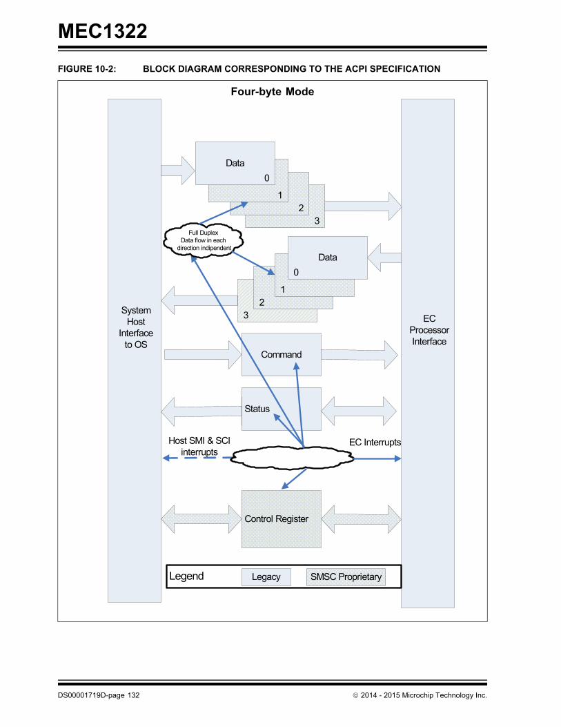
MEC1322
Four-byte Mode
FIGURE 10-2: BLOCK DIAGRAM CORRESPONDING TO THE ACPI SPECIFICATION
Status
Command
System Host
Interface to OS
EC InterruptsHost SMI & SCI interrupts
ECProcessorInterface
Data
0
21
3
Data
0
21
3
Full DuplexData flow in each
direction indipendent
Control Register
Legend Legacy SMSC Proprietary
DS00001719D-page 132 2014 - 2015 Microchip Technology Inc.

MEC1322
10.11 Register Aliasing between Runtime and EC-Only Registers
Table 10-6, "Runtime Register Aliasing into EC-Only Registers" indicates the aliasing from Runtime registers to EC-Onlyregisters. The “Host/EC Access” column distinguishes the aliasing based on access type. See individual registerdescriptions for more details.
Table 10-7, "EC-Only Registers Summary" indicates the aliasing from EC-Only to Runtime registers. The “Host/ECAccess” column distinguishes the aliasing based on access type. See individual register descriptions for more details.
TABLE 10-6: RUNTIME REGISTER ALIASING INTO EC-ONLY REGISTERS
HostOffset
Runtime RegisterRegister Name (Mnemonic)
Host Access
EC Offset
Aliased EC-Only RegisterRegister Name (Mnemonic)
EC Access
00h ACPI OS Data Register Byte 0 Register
W 108h OS2EC Data EC Byte 0 Register R
00h ACPI OS Data Register Byte 0 Register
R 100h EC2OS Data EC Byte 0 Register W
01h ACPI OS Data Register Byte 1 Register
W 109h OS2EC Data EC Byte 1 Register R
01h ACPI OS Data Register Byte 1 Register
R 101h EC2OS Data EC Byte 1 Register W
02h ACPI OS Data Register Byte 2 Register
W 10Ah OS2EC Data EC Byte 2 Register R
02h ACPI OS Data Register Byte 2 Register
R 102h EC2OS Data EC Byte 2 Register W
03h ACPI OS Data Register Byte 3 Register
W 10Bh OS2EC Data EC Byte 3 Register R
03h ACPI OS Data Register Byte 3 Register
R 103h EC2OS Data EC Byte 3 Register W
04h ACPI OS COMMAND Register W 108h OS2EC Data EC Byte 0 Register R
04h OS STATUS OS Register R 104h EC STATUS Register W
05h OS Byte Control Register R 105h EC Byte Control Register R/W
06h Reserved 106h Reserved
07h Reserved 107h Reserved
TABLE 10-7: EC-ONLY REGISTERS SUMMARY
ECOffset
EC-Only RegistersRegister Name (Mnemonic)
EC Access
HostOffset
Aliased Runtime RegisterRegister Name (Mnemonic)
Host Access
108h OS2EC Data EC Byte 0 Register R 00h ACPI OS Data Register Byte 0 Register
W
108h OS2EC Data EC Byte 0 Register R 04h ACPI OS COMMAND Register W
109h OS2EC Data EC Byte 1 Register R 01h ACPI OS Data Register Byte 1 Register
W
10Ah OS2EC Data EC Byte 2 Register R 02h ACPI OS Data Register Byte 2 Register
W
10Bh OS2EC Data EC Byte 3 Register R 03h ACPI OS Data Register Byte 3 Register
W
104h EC STATUS Register W 04h OS STATUS OS Register W
105h EC Byte Control Register R/W 05h OS Byte Control Register R
106h Reserved R Reserved R
107h Reserved R Reserved R
100h EC2OS Data EC Byte 0 Register W 00h ACPI OS Data Register Byte 0 Register
R
2014 - 2015 Microchip Technology Inc. DS00001719D-page 133
MEC1322
10.12 Runtime Registers
The registers listed in the Runtime Register Summary table are for two instances of the ACPI Embedded ControllerInterface (ACPI-ECI). The addresses of each register listed in this table are defined as a relative offset to the host“Base Address” defined in the Runtime Register Base Address Table.
The Base Address indicates where the first register can be accessed in a particular address space for a block instance
10.12.1 ACPI OS DATA REGISTER BYTE 0 REGISTER
This register is aliased; see ACPI-OS DATA BYTES[3:0] on page 135, OS2EC DATA BYTES[3:0] on page 141, andEC2OS DATA BYTES[3:0] on page 142 for detailed description of access rules.
101h EC2OS Data EC Byte 1 Register W 01h ACPI OS Data Register Byte 1 Register
R
102h EC2OS Data EC Byte 2 Register W 02h ACPI OS Data Register Byte 2 Register
R
103h EC2OS Data EC Byte 3 Register W 03h ACPI OS Data Register Byte 3 Register
R
Note: The Runtime registers may be accessed by the EC but typically the Host will access the Runtime Registersand the EC will access just the EC-Only registers.
TABLE 10-8: RUNTIME REGISTER BASE ADDRESS TABLE
Block InstanceInstance Number
Host Address Space Base Address
ACPI-EC 0 LPC I/O Programmed BAR
EC 32-bit internal address space
400F_0C00h
ACPI-EC 1 LPC I/O Programmed BAR
EC 32-bit internal address space
400F_1000h
TABLE 10-9: RUNTIME REGISTER SUMMARY
Offset Register Name (Mnemonic)
00h ACPI OS Data Register Byte 0 Register
01h ACPI OS Data Register Byte 1 Register
02h ACPI OS Data Register Byte 2 Register
03h ACPI OS Data Register Byte 3 Register
04h ACPI OS COMMAND Register
04h OS STATUS OS Register
05h OS Byte Control Register
06h Reserved
07h Reserved
Offset 00h
Bits Description Type DefaultReset Event
7:0 ACPI_OS_DATA_BYTE_0
This is byte 0 of the 32-bit ACPI-OS DATA BYTES[3:0].
R/W 0h VCC1_RESET
TABLE 10-7: EC-ONLY REGISTERS SUMMARY (CONTINUED)
ECOffset
EC-Only RegistersRegister Name (Mnemonic)
EC Access
HostOffset
Aliased Runtime RegisterRegister Name (Mnemonic)
Host Access
DS00001719D-page 134 2014 - 2015 Microchip Technology Inc.
MEC1322
ACPI-OS DATA BYTES[3:0]
Writes by the ACPI_OS to the ACPI-OS DATA BYTES[3:0] are aliased to the OS2EC DATA BYTES[3:0]. Reads by theACPI_OS from the ACPI-OS DATA BYTES[3:0] are aliased to the EC2OS DATA BYTES[3:0].
All access to the ACPI-OS DATA BYTES[3:0] registers should be orderly: Least Significant Byte to Most Significant Bytewhen byte access is used.
Writes to any of the four ACPI-OS DATA BYTES[3:0] registers clears the CMD bit in the OS STATUS OS Register (thestate of the FOUR_BYTE_ACCESS bit in the OS Byte Control Register has no impact.)
When the FOUR_BYTE_ACCESS bit in the OS Byte Control Register is cleared to ‘0’, the following access rules apply:
1. Writes to the ACPI OS Data Register Byte 0 Register sets the IBF bit in the OS STATUS OS Register.
2. Reads from the ACPI OS Data Register Byte 0 Register clears the OBF bit in the OS STATUS OS Register.
3. All writes to ACPI-OS DATA BYTES[3:1] complete without error but the data are not registered.
4. All reads from ACPI-OS DATA BYTES[3:1] return 00h without error.
5. Access to ACPI-OS DATA BYTES[3:1] has no effect on the IBF & OBF bits in the OS STATUS OS Register.
When the Four Byte Access bit in the OS Byte Control Register is set to ‘1’, the following access rules apply:
1. Writes to the ACPI OS Data Register Byte 3 Register sets the IBF bit in the OS STATUS OS Register.
2. Reads from the ACPI OS Data Register Byte 3 Register clears the OBF bit in the OS STATUS OS Register.
10.12.2 ACPI OS DATA REGISTER BYTE 1 REGISTER
This register is aliased; see ACPI-OS DATA BYTES[3:0] on page 135, OS2EC DATA BYTES[3:0] on page 141, andEC2OS DATA BYTES[3:0] on page 142 for detailed description of access rules.
10.12.3 ACPI OS DATA REGISTER BYTE 2 REGISTER
This register is aliased; see ACPI-OS DATA BYTES[3:0] on page 135, OS2EC DATA BYTES[3:0] on page 141, andEC2OS DATA BYTES[3:0] on page 142 for detailed description of access rules.
10.12.4 ACPI OS DATA REGISTER BYTE 3 REGISTER
This register is aliased; see ACPI-OS DATA BYTES[3:0] on page 135, OS2EC DATA BYTES[3:0] on page 141, andEC2OS DATA BYTES[3:0] on page 142 for detailed description of access rules.
Offset 01h
Bits Description Type DefaultReset Event
7:0 ACPI_OS_DATA_BYTE_1
This is byte 1 of the 32-bit ACPI-OS DATA BYTES[3:0].
R/W 0h VCC1_RESET
Offset 02h
Bits Description Type DefaultReset Event
7:0 ACPI_OS_DATA_BYTE_2
This is byte 2 of the 32-bit ACPI-OS DATA BYTES[3:0].
R/W 0h VCC1_RESET
Offset 03h
Bits Description Type DefaultReset Event
7:0 ACPI_OS_DATA_BYTE_3
This is byte 3 of the 32-bit ACPI-OS DATA BYTES[3:0].
R/W 0h VCC1_RESET
2014 - 2015 Microchip Technology Inc. DS00001719D-page 135

MEC1322
10.12.5 ACPI OS COMMAND REGISTER
10.12.6 OS STATUS OS REGISTER
This read-only register is aliased to the EC STATUS Register on page 143. the EC STATUS Register on page 143 hasread write access.
Offset 04h
Bits Description Type DefaultReset Event
7:0 ACPI_OSS_COMMAND
Writes to the this register are aliased in the OS2EC Data EC Byte 0 Register.
Writes to the this register also set the CMD and IBF bits in the OS STATUS OS Register
W 0h VCC1_RESET
Offset 04h
Bits Description Type DefaultReset Event
7 UD0B
User Defined
R 0b VCC1_RESET
6 SMI_EVT
This bit is set when an SMI event is pending; i.e., the ACPI_EC is requesting an SMI query; This bit is cleared when no SMI events are pending.This bit is an ACPI_EC-maintained software flag that is set when the ACPI_EC has detected an internal event that requires system management interrupt handler attention. The ACPI_EC sets this bit before generating an SMI.
Note: The usage model from the ACPI specification requiresboth SMI’s and SCI’s. The ACPI_OS SMI & SCI inter-rupts are not implemented in the ACPI Embedded Con-troller Interface (ACPI-ECI). The SMI_EVT andSCI_EVT bits in the OS STATUS OS Register are soft-ware flags and this block do not initiate SMI or SCIevents.
R 0b VCC1_RESET
5 SCI_EVT
This bit is set by software when an SCI event is pending; i.e., the ACPI_EC is requesting an SCI query; SCI Event flag is clear when no SCI events are pending.This bit is an ACPI_EC-maintained software flag that is set when the embedded controller has detected an internal event that requires operating system attention. The ACPI_EC sets this bit before generating an SCI to the OS.
Note: The usage model from the ACPI specification requiresboth SMI’s and SCI’s. The ACPI_OS SMI & SCI inter-rupts are not implemented in the ACPI Embedded Con-troller Interface (ACPI-ECI). The SMI_EVT andSCI_EVT bits in the OS STATUS OS Register are soft-ware flags and this block do not initiate SMI or SCIevents.
R 0b VCC1_RESET
DS00001719D-page 136 2014 - 2015 Microchip Technology Inc.

MEC1322
4 BURST
The BURST bit is set when the ACPI_EC is in Burst Mode for polled command processing; the BURST bit is cleared when the ACPI_EC is in Normal mode for interrupt-driven command processing.The BURST bit is an ACPI_EC-maintained software flag that indi-cates the embedded controller has received the Burst Enable com-mand from the host, has halted normal processing, and is waiting for a series of commands to be sent from the host. Burst Mode allows the OS or system management handler to quickly read and write several bytes of data at a time without the overhead of SCIs between commands.The BURST bit is maintained by ACPI_EC software, only.
R 0b VCC1_RESET
3 CMD
This bit is set when the OS2EC Data EC Byte 0 Register contains a command byte written into ACPI OS COMMAND Register; this bit is cleared when the OS2EC DATA BYTES[3:0] contains a data byte written into the ACPI-OS DATA BYTES[3:0].
This bit is hardware controlled: • ACPI_OS writes to any of the four ACPI-OS DATA BYTES[3:0]
bytes clears this bit• ACPI_OS writes to the ACPI OS COMMAND Register sets this
bit.
Note: This bit allows the embedded controller to differentiatethe start of a command sequence from a data byte writeoperation.
R 0b VCC1_RESET
2 UD1B
User Defined
R 0b VCC1_RESET
Offset 04h
Bits Description Type DefaultReset Event
2014 - 2015 Microchip Technology Inc. DS00001719D-page 137
MEC1322
1 IBF
The Input Buffer Full bit is set to indicate that a the ACPI_OS has written a command or data to the ACPI_EC and that data is ready. This bit is automatically cleared when data has been read by the ACPI_EC.
Note: The setting and clearing of this IBF varies depending onthe setting of the following bits: CMD bit in this registerand FOUR_BYTE_ACCESS bit in the OS Byte ControlRegister. Three scenarios follow:
1. The IBF is set when the ACPI_OS writes to the ACPI OSCOMMAND Register. This same write autonomously sets theCMD bit in this register.
The IBF is cleared if the CMD bit in this register is set and the ACPI_EC reads from the OS2EC Data EC Byte 0 Register.
Note: When CMD bit in this register is set the FOUR_BYTE_-ACCESS bit in the OS Byte Control Register has noimpact on the IBF bit behavior.
2. A write by the to the ACPI_OS to the ACPI OS Data RegisterByte 0 Register sets the IBF bit if the FOUR_BYTE_ACCESSbit in the OS Byte Control Register is in the cleared to ‘0’ stateprior to this write. This same write autonomously clears theCMD bit in this register.
A read of the OS2EC Data EC Byte 0 Register clears the IBF bit if the FOUR_BYTE_ACCESS bit in the OS Byte Control Register is in the cleared to ‘0’ state prior to this read.
3. A write by the to the ACPI_OS to the ACPI OS Data RegisterByte 3 Register sets the IBF bit if the FOUR_BYTE_ACCESSbit in the OS Byte Control Register is in the set to ‘1’ state priorto this write. This same write autonomously clears the CMDbit in this register.
A read of the OS2EC Data EC Byte 3 Register clears the IBF bit if the FOUR_BYTE_ACCESS bit in the OS Byte Control Register is in the set to ‘1’ state prior to this read.
An EC_IBF interrupt signals the ACPI_EC that there is data avail-able. The ACPI Specification usage model is as follows:
1. The ACPI_EC reads the EC STATUS Register and sees theIBF flag set,
2. The ACPI_EC reads all the data available in the OS2ECDATA BYTES[3:0]. This causes the IBF bit to be automaticallycleared by hardware.
3. The ACPI_EC must then generate a software interrupt (SeeNote: on page 130) to alert the ACPI_OS that the data hasbeen read and that the host is free to write more data to theACPI_EC as needed.
R 0h VCC1_RESET
Offset 04h
Bits Description Type DefaultReset Event
DS00001719D-page 138 2014 - 2015 Microchip Technology Inc.

MEC1322
0 OBF
The Output Buffer Full bit is set to indicate that a the ACPI_EC has written a data to the ACPI_OS and that data is ready. This bit is automatically cleared when all the data has been read by the ACPI_OS.
Note: The setting and clearing of this OBF varies dependingon the setting FOUR_BYTE_ACCESS bit in the OS ByteControl Register. Two scenarios follow:
1. The OBF bit is set if the Four Byte Access bit in the OS ByteControl Register is ‘0’ when the ACPI_EC writes to theEC2OS Data EC Byte 0 Register.
The OBF is cleared if the Four Byte Access bit in the OS Byte Con-trol Register is cleared to ‘0’ when the ACPI_OS reads from the ACPI OS Data Register Byte 0 Register.
2. The OBF is set if the Four Byte Access bit in the OS Byte Con-trol Register is set to ‘1’ when the ACPI_EC writes to theEC2OS Data EC Byte 3 Register.
The OBF is cleared if the Four Byte Access bit in the OS Byte Con-trol Register is set to ‘1’ when the ACPI_OS reads from the ACPI OS Data Register Byte 3 Register.
The ACPI Specification usage model is as follows:
1. The ACPI_EC must generate a software interrupt (See Note:on page 130) to alert the ACPI_OS that the data is available.
2. The ACPI_OS reads the OS STATUS OS Register and seesthe OBF flag set, the ACPI_OS reads all the data available inthe ACPI-OS DATA BYTES[3:0].
3. The ACPI_OS reads all the data available in the ACPI-OSDATA BYTES[3:0]. This causes the OBF bit to be automati-cally cleared by hardware and the associated EC_OBF inter-rupt to be asserted.
R 0h VCC1_RESET
Offset 04h
Bits Description Type DefaultReset Event
2014 - 2015 Microchip Technology Inc. DS00001719D-page 139

MEC1322
10.12.7 OS BYTE CONTROL REGISTER
This register is aliased to the EC Byte Control Register on page 144. No behavioral differences occur due to addressaliasing.
10.13 EC-Only Registers
The registers listed in the EC-Only Register Summary table are for two instances of the ACPI Embedded ControllerInterface (ACPI-ECI). The addresses of each register listed in this table are defined as a relative offset to the host“Base Address” defined in the EC-Only Register Base Address Table.
The Base Address indicates where the first register can be accessed in a particular address space for a block instance.
Offset 05
Bits Description Type DefaultReset Event
7:1 Reserved R - -
0 FOUR_BYTE_ACCESS
When this bit is set to ‘1’, the ACPI Embedded Controller Interface (ACPI-ECI) accesses four bytes through the ACPI-OS DATA BYTES[3:0].When this bit is cleared to ‘0’, the ACPI Embedded Controller Inter-face (ACPI-ECI) accesses one byte through the ACPI OS Data Reg-ister Byte 0 Register. The corresponds to Legacy Mode described in Section 10.10, "Description," on page 130.
Note 1: This bit effects the behavior of the IBF & OBF bits in theOS STATUS OS Register.
2: See ACPI-OS DATA BYTES[3:0] on page 135, OS2ECDATA BYTES[3:0] on page 141, and EC2OS DATABYTES[3:0] on page 142 for detailed description ofaccess rules.
R 0b VCC1_RESET
Note: The ACPI_OS access Base Address Register (BAR) should be configured to match the access widthselected by the Four Byte Access bit in the OS Byte Control Register. This BAR in not described in thischapter.
TABLE 10-10: EC-ONLY REGISTER BASE ADDRESS TABLE
Block InstanceInstance Number
Host Address Space Base Address
ACPI-EC 0 EC 32-bit internal address space
400F_0C00h
ACPI-EC 1 EC 32-bit internal address space
400F_1000h
TABLE 10-11: EC-ONLY REGISTER SUMMARY
Offset Register Name (Mnemonic)
100h EC2OS Data EC Byte 0 Register
101h EC2OS Data EC Byte 1 Register
102h EC2OS Data EC Byte 2 Register
103h EC2OS Data EC Byte 3 Register
104h EC STATUS Register
105h EC Byte Control Register
106h Reserved
DS00001719D-page 140 2014 - 2015 Microchip Technology Inc.

MEC1322
10.13.1 OS2EC DATA EC BYTE 0 REGISTER
This register is aliased; see ACPI-OS DATA BYTES[3:0] on page 135, OS2EC DATA BYTES[3:0] on page 141, andEC2OS DATA BYTES[3:0] on page 142 for detailed description of access rules.
OS2EC DATA BYTES[3:0]
When the CMD bit in the OS STATUS OS Register is cleared to ‘0’, reads by the ACPI_EC from the OS2EC DATABYTES[3:0] are aliased to the ACPI-OS DATA BYTES[3:0].
All access to the OS2EC DATA BYTES[3:0] registers should be orderly: Least Significant Byte to Most Significant Bytewhen byte access is used.
When the FOUR_BYTE_ACCESS bit in the OS Byte Control Register is cleared to ‘0’, the following access rules apply:
1. Writes to the OS2EC DATA BYTES[3:0] have no effect on the OBF bit in the OS STATUS OS Register.
2. Reads from the OS2EC Data EC Byte 0 Register clears the IBF bit in the OS STATUS OS Register.
3. All reads from OS2EC DATA BYTES[3:1] return 00h without error.
4. Access to OS2EC DATA BYTES[3:1 has no effect on the IBF & OBF bits in the OS STATUS OS Register.
When the FOUR_BYTE_ACCESS bit in the OS Byte Control Register is set to ‘1’, the following access rules apply:
1. Writes to the OS2EC DATA BYTES[3:0] have no effect on the OBF bit in the OS STATUS OS Register.
2. Reads from the OS2EC Data EC Byte 3 Register clears the IBF bit in the OS STATUS OS Register.
10.13.2 OS2EC DATA EC BYTE 1 REGISTER
This register is aliased; see ACPI-OS DATA BYTES[3:0] on page 135, OS2EC DATA BYTES[3:0] on page 141, andEC2OS DATA BYTES[3:0] on page 142 for detailed description of access rules.
107h Reserved
108h OS2EC Data EC Byte 0 Register
109h OS2EC Data EC Byte 1 Register
10Ah OS2EC Data EC Byte 2 Register
10Bh OS2EC Data EC Byte 3 Register
Offset 108h
Bits Description Type DefaultReset Event
7:0 OS_TO_EC_DATA_BYTE_0
This is byte 0 of the 32-bit OS2EC DATA BYTES[3:0].
R/W 0h VCC1_RESET
Offset 109h
Bits Description Type DefaultReset Event
7:0 OS2EC_DATA_ BYTE_1
This is byte 1 of the 32-bit OS2EC DATA BYTES[3:0].
R/W 0h VCC1_RESET
TABLE 10-11: EC-ONLY REGISTER SUMMARY (CONTINUED)
Offset Register Name (Mnemonic)
2014 - 2015 Microchip Technology Inc. DS00001719D-page 141

MEC1322
10.13.3 OS2EC DATA EC BYTE 2 REGISTER
This register is aliased; see ACPI-OS DATA BYTES[3:0] on page 135, OS2EC DATA BYTES[3:0] on page 141, andEC2OS DATA BYTES[3:0] on page 142 for detailed description of access rules.
10.13.4 OS2EC DATA EC BYTE 3 REGISTER
This register is aliased; see ACPI-OS DATA BYTES[3:0] on page 135, OS2EC DATA BYTES[3:0] on page 141, andEC2OS DATA BYTES[3:0] on page 142 for detailed description of access rules.
10.13.5 EC2OS DATA EC BYTE 0 REGISTER
This register is aliased; see ACPI-OS DATA BYTES[3:0] on page 135, OS2EC DATA BYTES[3:0] on page 141, andEC2OS DATA BYTES[3:0] on page 142 for detailed description of access rules.
EC2OS DATA BYTES[3:0]
Writes by the ACPI_EC to the EC2OS DATA BYTES[3:0] are aliased to the ACPI-OS DATA BYTES[3:0]
All access to the EC2OS DATA BYTES[3:0] registers should be orderly: Least Significant Byte to Most Significant Bytewhen byte access is used.
When the FOUR_BYTE_ACCESS bit in the OS Byte Control Register is cleared to ‘0’, the following access rules apply:
1. Writes to the EC2OS Data EC Byte 0 Register set the OBF bit in the OS STATUS OS Register.
2. Reads from the EC2OS DATA BYTES[3:0] have no effect on the IBF bit in the OS STATUS OS Register.
3. All reads from EC2OS DATA BYTES[3:1] return 00h without error.
4. All writes to EC2OS DATA BYTES[3:1] complete without error but the data are not registered.
5. Access to EC2OS DATA BYTES[3:1] have no effect on the IBF & OBF bits in the OS STATUS OS Register.
When the FOUR_BYTE_ACCESS bit in the OS Byte Control Register is set to ‘1’, the following access rules apply:
1. Writes to the EC2OS Data EC Byte 3 Register set the OBF bit in the OS STATUS OS Register.
2. Reads from the EC2OS DATA BYTES[3:0] have no effect on the IBF bit in the OS STATUS OS Register.
Offset 10Ah
Bits Description Type DefaultReset Event
7:0 OS2EC_DATA_BYTE_2
This is byte 2 of the 32-bit OS2EC DATA BYTES[3:0].
R/W 0h VCC1_RESET
Offset 10Bh
Bits Description Type DefaultReset Event
7:0 OS2EC_DATA_BYTE_3
This is byte 3 of the 32-bit OS2EC DATA BYTES[3:0].
R/W 0h VCC1_RESET
Offset 100h
Bits Description Type DefaultReset Event
7:0 EC2OS_DATA_BYTE_0
This is byte 0 of the 32-bit EC2OS DATA BYTES[3:0].
R/W 0h VCC1_RESET
DS00001719D-page 142 2014 - 2015 Microchip Technology Inc.

MEC1322
10.13.6 EC2OS DATA EC BYTE 1 REGISTER
This register is aliased; see ACPI-OS DATA BYTES[3:0] on page 135, OS2EC DATA BYTES[3:0] on page 141, andEC2OS DATA BYTES[3:0] on page 142 for detailed description of access rules.
10.13.7 EC2OS DATA EC BYTE 2 REGISTER
This register is aliased; see ACPI-OS DATA BYTES[3:0] on page 135, OS2EC DATA BYTES[3:0] on page 141, andEC2OS DATA BYTES[3:0] on page 142 for detailed description of access rules.
10.13.8 EC2OS DATA EC BYTE 3 REGISTER
This register is aliased; see ACPI-OS DATA BYTES[3:0] on page 135, OS2EC DATA BYTES[3:0] on page 141, andEC2OS DATA BYTES[3:0] on page 142 for detailed description of access rules.
10.13.9 EC STATUS REGISTER
This register is aliased to the OS STATUS OS Register on page 136. The OS STATUS OS Register is a read only versionof this register.
Offset 101h
Bits Description Type DefaultReset Event
7:0 EC2OS_DATA_BYTE_1
This is byte 1 of the 32-bit EC2OS DATA BYTES[3:0].
R/W 0h VCC1_RESET
Offset 102h
Bits Description Type DefaultReset Event
7:0 EC2OS_DATA_BYTE_2
This is byte 2 of the 32-bit EC2OS DATA BYTES[3:0].
R/W 0h VCC1_RESET
Offset 103h
Bits Description Type DefaultReset Event
7:0 EC2OS_DATA_BYTE_3
This is byte 3 of the 32-bit EC2OS DATA BYTES[3:0].
R/W 0h VCC1_RESET
Offset 104h
Bits Description Type DefaultReset Event
7 UD0A
User Defined
R/W 0b VCC1_RESET
6 SMI_EVT
See SMI_EVT bit in OS STATUS OS Register on page 136 for bit description.
R/W 0b VCC1_RESET
5 SCI_EVT
See SMI_EVT bit in OS STATUS OS Register on page 136 for bit description.
R/W 0b VCC1_RESET
4 BURST
See BURST bit in OS STATUS OS Register on page 136 for bit description.
R/W 0b VCC1_RESET
2014 - 2015 Microchip Technology Inc. DS00001719D-page 143

MEC1322
10.13.10 EC BYTE CONTROL REGISTER
This register is aliased to the OS Byte Control Register on page 140. The OS Byte Control Register is a read only versionof this register.
3 CMD
See CMD bit in OS STATUS OS Register on page 136 for bit description.
R 0b VCC1_RESET
2 UD1A
User Defined
R/W 0b VCC1_RESET
1 IBF
See IBF bit in OS STATUS OS Register on page 136 for bit descrip-tion.
R 0h VCC1_RESET
0 OBF
See OBF bit in OS STATUS OS Register on page 136 for bit descrip-tion.
R 0h VCC1_RESET
Note: The IBF and OBF bits are not de-asserted by hardware when the host is powered off, or the LPC interfacepowers down; for example, following system state changes S3->S0, S5->S0, G3-> S0. For further informa-tion on how these bits are cleared, refer to IBF and OBF bit descriptions in the STATUS OS-Register defi-nition.
Offset 105h
Bits Description Type DefaultReset Event
7:1 Reserved R - -
0 FOUR_BYTE_ACCESSSee FOUR_BYTE_ACCESS bit in OS Byte Control Register on page 140 for bit description.
R/W 0b VCC1_RESET
Offset 104h
Bits Description Type DefaultReset Event
DS00001719D-page 144 2014 - 2015 Microchip Technology Inc.

MEC1322
11.0 8042 EMULATED KEYBOARD CONTROLLER
11.1 Introduction
The MEC1322 keyboard controller uses the EC to produce a superset of the features provided by the industry-standard8042 keyboard controller. The 8042 Emulated Keyboard Controller is a Host/EC Message Interface with hardwareassists to emulate 8042 behavior and provide Legacy GATEA20 support.
11.2 References
There are no references for this block.
11.3 Interface
This block is designed to be accessed externally via the pin interface and internally via a registered host interface.
11.4 Signal Description
Note: There is no VCC emulation in hardware for this interface.
FIGURE 11-1: I/O DIAGRAM OF BLOCK
TABLE 11-1: SIGNAL DESCRIPTION TABLE
Name Direction Description
KBRST Output Keyboard Reset, routed to pin
8042 Emulated Keyboard Controller
Signal DescriptionClock Inputs
Interrupts
Resets
Host Interface
2014 - 2015 Microchip Technology Inc. DS00001719D-page 145

MEC1322
11.5 Host Interface
The 8042 interface is accessed by host software via a registered interface, as defined in Section 11.13, "ConfigurationRegisters" and Section 11.14, "Runtime Registers".
11.6 Power, Clocks and Reset
This section defines the Power, Clock, and Reset parameters of the block.
11.6.1 POWER DOMAINS
11.6.2 CLOCK INPUTS
11.6.3 RESETS
11.7 Interrupts
This section defines the Interrupt Sources generated from this block.
11.8 Low Power Modes
The 8042 Interface may be put into a low power state by the chip’s Power, Clocks, and Reset (PCR) circuitry.
TABLE 11-2: POWER SOURCES
Name Description
VCC1 This Power Well is used to power the registers and logic in this block.
TABLE 11-3: CLOCK INPUTS
Name Description
1MHz Clock used for the counter in the CPU_RESET circuitry.
TABLE 11-4: RESET SIGNALS
Name Description
VCC1_RESET This reset is asserted when VCC1 is applied.
PWRGD This signal is asserted when the main power rail is asserted.
PCI RESET# This signal is asserted when LRESET# is asserted.
nSIO_RESET This signal is asserted when VCC1 is low, PWRGD is low, or LRESET# is asserted.
TABLE 11-5: SYSTEM INTERRUPTS
Source Description
KIRQ This interrupt source for the SIRQ logic, representing a Keyboard inter-rupt, is generated when the PCOBF status bit is ‘1’.
MIRQ This interrupt source for the SIRQ logic, representing a Mouse interrupt, is generated when the AUXOBF status bit is ‘1’.
TABLE 11-6: EC INTERRUPTS
Source Description
8042EM_IBF Interrupt generated by the host writing either data or command to the data register
8042EM_OBF Interrupt generated by the host reading either data or aux data from the data register
DS00001719D-page 146 2014 - 2015 Microchip Technology Inc.

MEC1322
11.9 Description
11.9.1 BLOCK DIAGRAM
11.10 EC-to-Host Keyboard Communication
The EC can write to the EC_HOST Data / AUX Data Register by writing to the HOST2EC Data Register at EC-Onlyoffset 0h or the EC AUX Data Register at EC-Only offset Ch. A write to either of these addresses automatically sets bit0 (OBF) in the Status register. A write to the HOST2EC Data Register may also set PCOBF. A write to the EC AUX DataRegister may also set AUXOBF.
11.10.1 PCOBF DESCRIPTION
If enabled by the bit OBFEN, the bit PCOBF is gated onto KIRQ. The KIRQ signal is a system interrupt which signifiesthat the EC has written to the HOST2EC Data Register (EC-Only offset 0h). On power-up, PCOBF is reset to 0. PCOBFwill normally reflect the status of writes to HOST2EC register, if PCOBFEN is “0”. PCOBF is cleared by hardware on aHOST read of the EC_HOST Data / AUX Data Register.
KIRQ is normally selected as IRQ1 for keyboard support.
Additional flexibility has been added which allows firmware to directly control the PCOBF output signal, independent ofdata transfers to the host-interface data output register. This feature allows the MEC1322 to be operated via the host“polled” mode. Firmware control is active when PCOBFEN is ‘1’. Firmware sets PCOBF high by writing a “1” to thePCOBF field of the PCOBF Register. Firmware must also clear PCOBF by writing a “0” to the PCOBF field.
The PCOBF register is also readable; the value read back on bit 0 of the register always reflects the present value ofthe PCOBF output. If PCOBFEN = 1, then this value reflects the output of the firmware latch in the PCOBF Register. IfPCOBFEN = 0, then the value read back reflects the in-process status of write cycles to the HOST2EC Data Register(i.e., if the value read back is high, the host interface output data register has just been written to). If OBFEN=0, thenKIRQ is driven inactive (low).
FIGURE 11-2: BLOCK DIAGRAM OF 8042 Emulated Keyboard Controller
SPB offset =100hRead Data or CMD
AUXH = 1 Bit [5] is AUXOBFAUXH = 0 Bit [5] is UD
2 IBF SET on Host Write to LPC I/O Index =00h or 04h
IBF Cleared on EC Read to SPB Offset = 00h
3 OBF SET on EC Write to SPB offset = 100h or 10ChOBF Cleared by Read 0f
LPC I/O Index 00h
4 PCOBFEN = 1 PCOBF is contents of Bit 0 SPB offset = 114hPCOBFEN = 0 PCBOBF is set on EC Write of SPB offset = 100 h
PCOBF is cleared on Host Read of LPC I/O index = 00h
D7 D3D4D5D6 D0D1D2
D7UD
D3C/D
D4UD
D5AUXOBF / UD
D6UD
D0OBF3
D1IBF2
D2UD1
HOST_EC Data register
Status Register
Keyboard Control Register
WLPC I/O Index =00
Write Data
R
LPC I/O read index =04h
R
SPB offset =104h
R
W
EC Access
Host Access
1 This bit is reset by LPCRESET and VTR_POR
D7RES
D3RES
D4RES
D5RES
D6RES
D1RES
D2RES
PCOBF Register
R
FF_0514W
D7AUXH
D3UD
D4UD
D5OBFEN
D6UD
D0UD
D1SAEN
D2PCOBFEN
R
W
D7 D3D4D5D6 D0D1D2
R W
EC_HOST Data Register
SPB offset =10ChWrite Aux Data
SPB offset =100hWrite Data
FF_0508
D0PCOBF4
LPC I/O Index =04Write CMD
LPC I/O Index =00Read Data or AUX Data
2014 - 2015 Microchip Technology Inc. DS00001719D-page 147

MEC1322
11.10.2 AUXOBF DESCRIPTION
If enabled by the bit OBFEN, the bit AUXOBF is multiplexed onto MIRQ. The AUXOBF/MIRQ signal is a system interruptwhich signifies that the EC has written to the EC_HOST Data / AUX Data Register. On power-up, after VCC1_RESET,AUXOBF is reset to 0. AUXOBF will normally reflects the status of writes to EC EC AUX Data Register (EC-Only offsetCh). AUXOBF is cleared by hardware on a read of the Host Data Register. If OBFEN=0, then MIRQ is driven inactive(low).
MIRQ is normally selected as IRQ12 for mouse support.
Firmware can also directly control the AUXOBF output signal, similar to the mechanism it can use to control PCOBF.Firmware control is active when AUXH is ‘0’. Firmware sets AUXOBF high by writing a “1” to the AUXOBF field of theEC Keyboard Status Register. Firmware must also clear AUXOBF by writing a “0” to the AUXOBF field.
11.11 Legacy Port92/GATEA20 Support
The MEC1322 supports LPC I/O writes to port HOST I/O address 92h as a quick alternate mechanism for generating aCPU_RESET pulse or controlling the state of GATEA20. The Port92/GateA20 logic has a separate Logical Device Num-ber and Base Address register (see Section 11.16, "Legacy Port92/GATEA20 Configuration Registers" and Section11.17, "Legacy Port92/GATEA20 Runtime Registers". The Base Address Register for the Port92/GateA20 LogicalDevice has only one writable bit, the Valid Bit, since the only I/O accessible Register has a fixed address.
The Port 92 Register resides at HOST I/O address 92h and is used to support the alternate reset (ALT_RST#) and alter-nate GATEA20 (ALT_A20) functions. This register defaults to 00h on assertion of nSIO_RESET.
Setting the Port92 Enable bit (Port 92 Enable Register) enables the Port92h Register. When Port92 is disabled, by clear-ing the Port92 Enable bit, then access to this register is completely disabled (I/O writes to host 92h are ignored and I/Oreads float the system data bus SD[7:0]).
11.11.1 GATE A20 SPEEDUP
The MEC1322 contains on-chip logic support for the GATEA20 hardware speed-up feature. GATEA20 is part of the con-trol required to mask address line A20 to emulate 8086 addressing.
In addition to the ability for the host to control the GATEA20 output signal directly, a configuration bit called SAEN in theKeyboard Control Register is provided; when set, SAEN allows firmware to control the GATEA20 output. When SAENis set, a 1 bit register (GATEA20 Control Register) controls the GATEA20 output.
Host control and firmware control of GATEA20 affect two separate register elements. Read back of GATEA20 throughthe use of EC OFFSET 100h reflects the present state of the GATEA20 output signal: if SAEN is set, the value readback corresponds to the last firmware-initiated control of GATEA20; if SAEN is reset, the value read back correspondsto the last host-initiated control of GATEA20.
Host control of the GATEA20 output is provided by the hardware interpretation of the “GATEA20 sequence” (seeTable 11-9, "GATEA20 Command/Data Sequence Examples"). The foregoing description assumes that the SAEN con-figuration bit is reset.
TABLE 11-7: OBFEN AND PCOBFEN EFFECTS ON KIRQ
OBFEN PCOBFEN
0 X KIRQ is inactive and driven low
1 0 KIRQ = PCOBF (status of writes to HOST2EC Data Register)
1 1 KIRQ = PCOBF (status of writes to PCOBF Register)
TABLE 11-8: OBFEN AND AUXH EFFECTS ON MIRQ
OBFEN AUXH
0 X MIRQ is inactive and driven low
1 0 MIRQ = AUXOBF (status of writes to EC AUX Data Register)
1 1 MIRQ = AUXOBF (status of writes to AUXOBF in EC Keyboard Status Register)
DS00001719D-page 148 2014 - 2015 Microchip Technology Inc.

MEC1322
When the MEC1322 receives a “D1” command followed by data (via the host interface), the on-chip hardware copiesthe value of data bit 1 in the received data field to the GATEA20 host latch. At no time during this host-interface trans-action will PCOBF or the IBF flag (bit 1) in the EC Keyboard Status Register be activated; for example, this host controlof GATEA20 is transparent to firmware, with no consequent degradation of overall system performance. Table 11-9details the possible GATEA20 sequences and the MEC1322 responses.
An additional level of control flexibility is offered via a memory-mapped synchronous set and reset capability. Any datawritten to the SETGA20L Register causes the GATEA20 host latch to be set; any data written to the RSTGA20L Registercauses it to be reset. This control mechanism should be used with caution. It was added to augment the “normal” controlflow as described above, not to replace it. Since the host and the firmware have asynchronous control capability of thehost latch via this mechanism, a potential conflict could arise. Therefore, after using the SETGA20L and RSTGA20Lregisters, firmware should read back the GATEA20 status via the GATEA20 Control Register (with SAEN = 0) to confirmthe actual GATEA20 response.
TABLE 11-9: GATEA20 COMMAND/DATA SEQUENCE EXAMPLES
Data Byte
R/W D[0:7] IBF Flag GATEA20 Comments
101
WWW
D1DFFF
000
Q11
GATEA20 Turn-on Sequence
101
WWW
D1DDFF
000
Q00
GATEA20 Turn-off Sequence
1101
WWWW
D1D1DFFF
0000
QQ11
GATEA20 Turn-on Sequence(*)
1101
WWWW
D1D1DDFF
0000
QQ00
GATEA20 Turn-off Sequence(*)
111
WWW
D1XX**FF
011
QQQ
Invalid Sequence
Note: The following notes apply:
- All examples assume that the SAEN configuration bit is 0.
- “Q” indicates the bit remains set at the previous state.
- *Not a standard sequence.
- **XX = Anything except D1.
- If multiple data bytes, set IBF and wait at state 0. Let the software know something unusual happened.
- For data bytes, only D[1] is used; all other bits are don't care.
- Host Commands (FF, FE, & D1) do not cause IBF. The method of blocking IBF in Figure 11-4 is the nIOW not being asserted when FF, FE, & D1 Host commands are written”.
2014 - 2015 Microchip Technology Inc. DS00001719D-page 149

MEC1322
The hardware GATEA20 state machine returns to state S1 from state S2 when CMD = D1, as shown in the followingfigures:.
FIGURE 11-3: GATEA20 STATE MACHINE
S0
S2 S1
RESET
CMD !=D1 orDATA[IBF=1]
CMD = FF[IBF=0] CMD !=D1
orCMD !=FF orDATA[IBF=1]
CMD !=D1[IBF=1]
CMD = D1[IBF=0]
CMD = D1[IBF=0]
Data[IBF=0, Latch DIN
CMD = D1[IBF=0]
Notes: GateA20 Changes When in S1 going to S2 Clock = wrdinB CMD = [C/D=1] Data = [C/D=0]
DS00001719D-page 150 2014 - 2015 Microchip Technology Inc.

MEC1322
11.11.2 CPU_RESET HARDWARE SPEED-UP
The ALT_CPU_RESET bit generates, under program control, the ALT_RST# signal, which provides an alternate, meansto drive the MEC1322 CPU_RESET pin which in turn is used to reset the Host CPU. The ALT_RST# signal is internallyNANDed together with the KBDRESET# pulse from the KRESET Speed up logic to provide an alternate software meansof resetting the host CPU.
Before another ALT_RST# pulse can be generated, ALT_CPU_RESET must be cleared to ‘0’ either by an nSIO_RESETor by a write to the Port 92 Register with bit 0 = ‘0’. An ALT_RST# pulse is not generated in the event that theALT_CPU_RESET bit is cleared and set before the prior ALT_RESET# pulse has completed.
If the 8042EM Sleep Enable is asserted, or the 8042 EM ACTIVATE bit is de-asserted, the 1MHz clocks source is dis-abled.
FIGURE 11-4: GATEA20 IMPLEMENTATION DIAGRAM
Q
Q
SET
CLRD
Q
QSET
CLR
D
Q
QSET
CLR
D
Q
QSET
CLR
D
SAEN
64&AEN#
Data
AEN#&60
Address
Q
QSET
CLR
D
Q
QSET
CLR
DSETGA20L Reg (Any WR)
RSTGA20L Reg (Any WR)
24MHz
IOW#
AEN#&64
GATEA20 Reg WR (D0)
GATEA20 Reg RD (D0)
CPU RESET
SD[7:0] = FE
SD[7:0] = FF
SD[7:0] = D1
IOW#
nIOW
nIOW
nIOW
IOW#
AEN#&60
KRESET Gen
IBF
ENAB P92
Port 92 Reg (D1)
GATEA20VCC
VCC
2014 - 2015 Microchip Technology Inc. DS00001719D-page 151

MEC1322
11.12 Instance Description
There are two blocks defined in this chapter: Emulated 8042 Interface and the Legacy Port92/GATEA20 Support. TheMEC1322 has one instance of each block.
11.13 Configuration Registers
The registers listed in the Configuration Register Summary table are for a single instance of the Emulated 8042 Inter-face. The addresses of each register listed in this table are defined as a relative offset to the host “Base Address” definedin the Configuration Register Base Address Table.
Each Configuration register access through the Host Access Port is via its LDN and its Host Access Port Index. ECaccess is a relative offset to the EC Base Address.
FIGURE 11-5: CPU_RESET IMPLEMENTATION DIAGRAM
TABLE 11-10: CONFIGURATION REGISTER BASE ADDRESS TABLE
Block InstanceInstance Number
LogicalDeviceNumber
Host Address Space Base Address
Emulated 8042 Interface
0 1 LPC Configuration Port INDEX = 00h
EC 32-bit internal address space
400F_0400h
TABLE 11-11: CONFIGURATION REGISTER SUMMARY
Offset Register Name (Mnemonic)
30h Activate Register
Pulse Generator
FE Command(From KRESETSpeed-up Logic)
Pulse Generator
SAEN
ENAB P92
CPU_RESET
6 μs14 μs
6 μs14 μs
KRESET
ALT_RST#Port 92 Reg (D0)
DS00001719D-page 152 2014 - 2015 Microchip Technology Inc.

MEC1322
11.13.1 ACTIVATE REGISTER
11.14 Runtime Registers
The registers listed in the Runtime Register Summary table are for a single instance of the Emulated 8042 Interface.The addresses of each register listed in this table are defined as a relative offset to the host “Base Address” defined inthe Runtime Register Base Address Table.
The Base Address indicates where the first register can be accessed in a particular address space for a block instance.
11.14.1 HOST_EC DATA / CMD REGISTER
Offset 30h
Bits Description Type DefaultReset Event
7:1 Reserved R - -
0 ACTIVATE
1=The 8042 Interface is powered and functional. 0=The 8042 Interface is powered down and inactive.
R/W 0b PWRGDand
VCC1_RESET
Block Instance Instance Number Host Address Space Base Address
Emulated 8042 Interface
0 LPC I/O Programmed BAR
EC 32-bit address space
400F_0400h
TABLE 11-12: RUNTIME REGISTER SUMMARY
Offset Register Name (Mnemonic)
00h/04h HOST_EC Data / CMD Register
00h EC_HOST Data / AUX Data Register
04h Keyboard Status Read Register
Offset 00h
Bits Description Type DefaultReset Event
7:0 WRITE_DATA
This 8-bit register is write-only. When written, the C/D bit in the Key-board Status Read Register is cleared to ‘0’, signifying data, and the IBF in the same register is set to ‘1’.
When the Runtime Register at offset 0h is read by the Host, it func-tions as the EC_HOST Data / AUX Data Register.
W 0h VCC1_RESET
2014 - 2015 Microchip Technology Inc. DS00001719D-page 153

MEC1322
11.14.2 EC_HOST DATA / AUX DATA REGISTER
11.14.3 KEYBOARD STATUS READ REGISTER
This register is a read-only alias of the EC Keyboard Status Register.
Offset 04h
Bits Description Type DefaultReset Event
7:0 WRITE_CMD
This 8-bit register is write-only and is an alias of the register at offset 0h. When written, the C/D bit in the Keyboard Status Read Register is set to ‘1’, signifying a command, and the IBF in the same register is set to ‘1’.
When the Runtime Register at offset 4h is read by the Host, it func-tions as the Keyboard Status Read Register.
W 0h VCC1_RESET
Offset 00h
Bits Description Type DefaultReset Event
7:0 READ_DATA
This 8-bit register is read-only. When read by the Host, the PCOBF and/or AUXOBF interrupts are cleared and the OBF flag in the status register is cleared.
R 0h VCC1_RESET
Offset 04h
Bits Description Type DefaultReset Event
7:6 UD2
User-defined data. Readable and writable by the EC when written by the EC at its EC-only alias.
R 0h VCC1_RESET
5 AUXOBF
Auxiliary Output Buffer Full. This bit is set to “1” whenever the EC writes the EC AUX Data Register. This flag is reset to “0” whenever the EC writes the EC Data Register.
R 0h VCC1_RESET
4 UD1
User-defined data. Readable and writable by the EC when written by the EC at its EC-only alias.
R 0h VCC1_RESET
3 C/D
Command Data. This bit specifies whether the input data register contains data or a command (“0” = data, “1” = command). During a Host command write operation (when the Host writes the HOST_EC Data / CMD Register at offset 04h), this bit is set to “1”. During a Host data write operation (when the Host writes the HOST_EC Data / CMD Register at offset 0h), this bit is set to “0”.
R 0h VCC1_RESET
2 UD0
User-defined data. Readable and writable by the EC when written by the EC at its EC-only alias.
Note: This bit is reset to ‘0’ when the LRESET# pin signal isasserted.
R 0h VCC1_RESET and
PCI RESET#
DS00001719D-page 154 2014 - 2015 Microchip Technology Inc.

MEC1322
11.15 Emulated 8042 Interface EC-Only Registers
The registers listed in the EC-Only Register Summary table are for a single instance of the Emulated 8042 Interface.The addresses of each register listed in this table are defined as a relative offset to the host “Base Address” defined inthe EC-Only Register Base Address Table.
The Base Address indicates where the first register can be accessed in a particular address space for a block instance.
1 IBF
Input Buffer Full. This bit is set to “1” whenever the Host writes dataor a command into the HOST_EC Data / CMD Registerr. When thisbit is set, the EC's 8042EM_IBF interrupt is asserted, if enabled.When the EC reads the HOST_EC Data/CMD Register, this bit isautomatically reset and the interrupt is cleared.
Note: This bit is not reset when PWRGD is asserted or whenthe LPC interface powers down. To clear this bit, firm-ware must read the EC Data Register in the EC-Onlyaddress space.
R 0h VCC1_RESET
0 OBF
Output Buffer Full. This bit is set when the EC writes a byte of Dataor AUX Data into the EC_HOST Data / AUX Data Register. Whenthe Host reads the HOST_EC Data / CMD Register, this bit is auto-matically cleared by hardware and a 8042EM_OBF interrupt is gen-erated.
Note: This bit is not reset when PWRGD is asserted or whenthe LPC interface powers down. To clear this bit, firm-ware must read the HOST_EC Data / CMD Register inthe Runtime address space.
R 0h VCC1_RESET
TABLE 11-13: EC-ONLY REGISTER BASE ADDRESS TABLE
Block Instance Instance Number Host Address Space Base Address
Emulated 8042 Interface
0 EC 32-bit address space
400F_0410h
TABLE 11-14: EC-ONLY REGISTER SUMMARY
Offset Register Name (Mnemonic)
0h HOST2EC Data Register
0h EC Data Register
4h EC Keyboard Status Register
8h Keyboard Control Register
Ch EC AUX Data Register
14h PCOBF Register
Offset 04h
Bits Description Type DefaultReset Event
2014 - 2015 Microchip Technology Inc. DS00001719D-page 155

MEC1322
11.15.1 HOST2EC DATA REGISTER
11.15.2 EC DATA REGISTER
11.15.3 EC KEYBOARD STATUS REGISTER
This register is an alias of the Keyboard Status Read Register. The fields C/D, IBF, and OBF remain read-only.
Offset 0h
Bits Description Type DefaultReset Event
7:0 HOST2EC_DATA
This register is an alias of the HOST_EC Data / CMD Register. When read at the EC-Only offset of 0h, it returns the data written by the Host to either Runtime Register offset 0h or Runtime Register offset 04h.
R 0h VCC1_RESET
Offset 0h
Bits Description Type DefaultReset Event
7:0 EC_DATA W 0h VCC1_RESET
Offset 04h
Bits Description Type DefaultReset Event
7:6 UD2
User-defined data. Readable and writable by the EC.
R/W 0h VCC1_RESET
5 AUXOBF
Auxiliary Output Buffer Full. This bit is set to ‘1’ whenever the EC writes the EC AUX Data Register. This flag is reset to ‘0’ whenever the EC writes the EC Data Register.
R/W 0h VCC1_RESET
4 UD1
User-defined data. Readable and writable by the EC when written by the EC at its EC-only alias.
R/W 0h VCC1_RESET
3 C/D
Command Data. This bit specifies whether the input data register contains data or a command. During a Host command write opera-tion (when the Host writes the HOST_EC Data / CMD Register at offset 04h), this bit is set to ‘1’. During a Host data write operation (when the Host writes the HOST_EC Data / CMD Register at offset 0h), this bit is set to ‘0’.
1=Command0=Data
R 0h VCC1_RESET
2 UD0
User-defined data. Readable and writable by the EC when written by the EC at its EC-only alias.
This bit is reset to ‘0’ when the LRESET# pin signal is asserted.
R/W 0h VCC1_RESET and
PCI RESET#
DS00001719D-page 156 2014 - 2015 Microchip Technology Inc.

MEC1322
11.15.4 KEYBOARD CONTROL REGISTER
1 IBF
Input Buffer Full. This bit is set to “1” whenever the Host writes dataor a command into the HOST_EC Data / CMD Registerr. When thisbit is set, the EC's 8042EM_IBF interrupt is asserted, if enabled.When the EC reads the Data/CMD Register, this bit is automaticallyreset and the interrupt is cleared.
This bit is not reset when PWRGD is asserted or when the LPC interface powers down. To clear this bit, firmware must read the EC Data Register in the EC-Only address space.
R 0h VCC1_RESET
0 OBF
Output Buffer Full. This bit is set when the EC writes a byte of Dataor AUX Data into the EC_HOST Data / AUX Data Register. Whenthe Host reads the HOST_EC Data / CMD Register, this bit is auto-matically cleared by hardware and a 8042EM_OBF interrupt is gen-erated.
This bit is not reset when PWRGD is asserted or when the LPC interface powers down. To clear this bit, firmware must read the Data/CMD Register in the Runtime address space.
R 0h VCC1_RESET
Offset 08h
Bits Description Type DefaultReset Event
7 AUXH
AUX in Hardware.
1=AUXOBF of the Keyboard Status Read Register is set in hardwareby a write to the EC AUX Data Register
0=AUXOBF is not modified in hardware, but can be read and writtenby the EC using the EC-Only alias of the EC Keyboard StatusRegister
R/W 0h VCC1_RESET
6 UD5
User-defined data. Readable and writable by the EC when written by the EC at its EC-only alias.
R/W 0h VCC1_RESET
5 OBFEN
When this bit is ‘1’, the system interrupt signal KIRQ is driven by thebit PCOBF and MIRQ is driven by AUXOBF. When this bit is ‘0’, KIRQand MIRQ are driven low.
This bit must not be changed when OBF of the status register is equalto ‘1’.
R/W 0h VCC1_RESET
4:3 UD4
User-defined data. Readable and writable by the EC when written by the EC at its EC-only alias.
R/W 0h VCC1_RESET
2 PCOBFEN
1= reflects the value written to the PCOBF Register0=PCOBF reflects the status of writes to the EC Data Register
R/W 0h VCC1_RESET
Offset 04h
Bits Description Type DefaultReset Event
2014 - 2015 Microchip Technology Inc. DS00001719D-page 157

MEC1322
11.15.5 EC AUX DATA REGISTER
11.15.6 PCOBF REGISTER
1 SAEN
Software-assist enable.
1=This bit allows control of the GATEA20 signal via firmware0=GATEA20 corresponds to either the last Host-initiated control of
GATEA20 or the firmware write to the Keyboard Control Registeror the EC AUX Data Register.
R/W 0h VCC1_RESET
0 UD3
User-defined data. Readable and writable by the EC when written by the EC at its EC-only alias.
R/W 0h VCC1_RESET
Offset 0Ch
Bits Description Type DefaultReset Event
7:0 EC_AUX_DATA
This 8-bit register is write-only. When written, the C/D in the Key-board Status Read Register is cleared to ‘0’, signifying data, and the IBF in the same register is set to ‘1’.
When the Runtime Register at offset 0h is read by the Host, it func-tions as the EC_HOST Data / AUX Data Register.
W 0h VCC1_RESET
Offset 14h
Bits Description Type DefaultReset Event
7:1 Reserved R - -
0 PCOBF
For a description of this bit, see Section 11.10.1, "PCOBF Descrip-tion".
R/W 0h VCC1_RESET
Offset 08h
Bits Description Type DefaultReset Event
DS00001719D-page 158 2014 - 2015 Microchip Technology Inc.

MEC1322
11.16 Legacy Port92/GATEA20 Configuration Registers
The registers listed in the Configuration Register Summary table are for a single instance of the LegacyPort92/GATEA20 logic. The addresses of each register listed in this table are defined as a relative offset to the host“Base Address” defined in the Configuration Register Base Address Table.
Each Configuration register access through the Host Access Port is via its LDN and its Host Access Port Index. ECaccess is a relative offset to the EC Base Address.
11.16.1 PORT 92 ENABLE REGISTER
11.17 Legacy Port92/GATEA20 Runtime Registers
The registers listed in the Runtime Register Summary table are for a single instance of the Legacy Port92/GATEA20logic. The addresses of each register listed in this table are defined as a relative offset to the host “Base Address”defined in the Runtime Register Base Address Table.
The Base Address indicates where the first register can be accessed in a particular address space for a block instance.
TABLE 11-15: CONFIGURATION BASE ADDRESS TABLE
Block InstanceInstance Number
LogicalDeviceNumber
Host Address Space Base Address
Port92-Legacy 0 1 LPC Configuration Port INDEX = 00h
EC 32-bit internal address space
400F_1800h
TABLE 11-16: CONFIGURATION REGISTER SUMMARY
Offset Register Name (Mnemonic)
30h Port 92 Enable Register
Offset 30h
Bits Description Type DefaultReset Event
7:1 Reserved R - -
0 P92_EN
When this bit is ‘1’, the Port92h Register is enabled. When this bit is ‘0’, the Port92h Register is disabled, and Host writes to LPC address 92h are ignored.
R/W 0h PWRGDand
VCC1_RESET
TABLE 11-17: RUNTIME REGISTER BASE ADDRESS TABLE
Block Instance Instance Number Host Address Space Base Address
Port92-Legacy 0 LPC I/O 0092h
EC 32-bit address space
400F_1800h
TABLE 11-18: RUNTIME REGISTER SUMMARY
Offset Register Name (Mnemonic)
0h Port 92 Register
2014 - 2015 Microchip Technology Inc. DS00001719D-page 159

MEC1322
11.17.1 PORT 92 REGISTER
11.18 Emulated 8042 Interface EC-Only Registers
The registers listed in the EC-Only Register Summary table are for a single instance of the Legacy Port92/GATEA20logic. The addresses of each register listed in this table are defined as a relative offset to the host “Base Address”defined in the EC-Only Register Base Address Table.
The Base Address indicates where the first register can be accessed in a particular address space for a block instance.
Offset 0h
Bits Description Type DefaultReset Event
7:2 Reserved R - -
1 ALT_GATE_A20
This bit provides an alternate means for system control of the GATEA20 pin. ALT_A20 low drives GATEA20 low, if A20 from the keyboard controller is also low. When Port 92 is enabled, writing a 1 to this bit forces ALT_A20 high. ALT_A20 high drives GATEA20 high regardless of the state of A20 from the keyboard controller.0=ALT_A20 is driven low1=ALT_A20 is driven high
R/W 0h nSIO_RESET
0 ALT_CPU_RESET
This bit provides an alternate means to generate a CPU_RESET pulse. The CPU_RESET output provides a means to reset the sys-tem CPU to effect a mode switch from Protected Virtual Address Mode to the Real Address Mode. This provides a faster means of reset than is provided through the EC keyboard controller. Writing a “1” to this bit will cause the ALT_RST# internal signal to pulse (active low) for a minimum of 6μs after a delay of 14μs. Before another ALT_RST# pulse can be generated, this bit must be written back to “0”.
R/W 0h nSIO_RESET
TABLE 11-19: EC-ONLY REGISTER BASE ADDRESS TABLE
Block Instance Instance Number Host Address Space Base Address
Port92-Legacy 0 EC 32-bit address space
400F_1900h
TABLE 11-20: EC-ONLY REGISTER SUMMARY
Offset Register Name (Mnemonic)
0h GATEA20 Control Register
8h SETGA20L Register
Ch RSTGA20L Register
DS00001719D-page 160 2014 - 2015 Microchip Technology Inc.

MEC1322
11.18.1 GATEA20 CONTROL REGISTER
11.18.2 SETGA20L REGISTER
11.18.3 RSTGA20L REGISTER
Offset 0h
Bits Description Type DefaultReset Event
7:1 Reserved R - -
0 GATEA20
0=The GATEA20 output is driven low1=The GATEA20 output is driven high
R/W 1h VCC1_RESET
Offset 08h
Bits Description Type DefaultReset Event
7:0 SETGA20L
See Section 11.11.1, "GATE A20 Speedup" for information on this register. A write to this register sets GATEA20 in the GATEA20 Con-trol Register.
W - -
Offset 0Ch
Bits Description Type DefaultReset Event
7:0 RSTGA20L
See Section 11.11.1, "GATE A20 Speedup" for information on this register. A write to this register sets GATEA20 in the GATEA20 Con-trol Register.
W - -
2014 - 2015 Microchip Technology Inc. DS00001719D-page 161
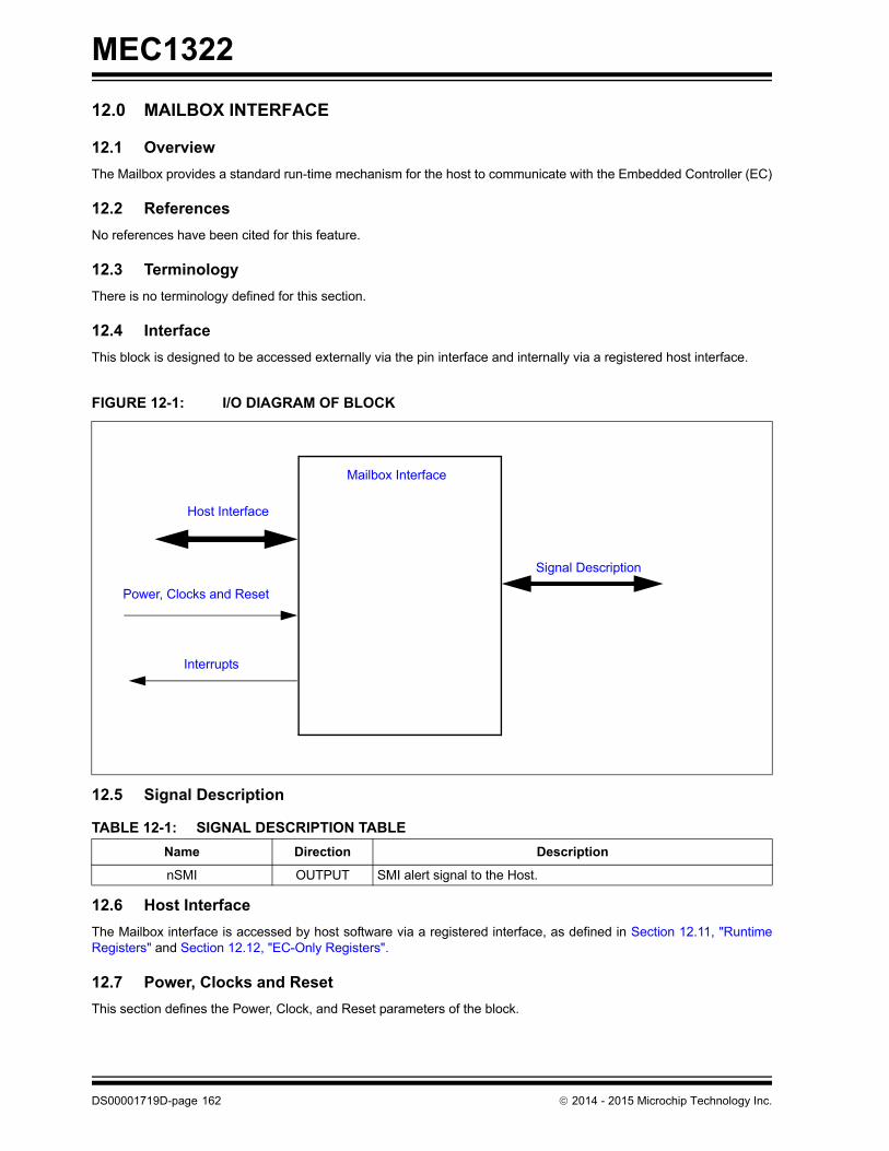
MEC1322
12.0 MAILBOX INTERFACE
12.1 Overview
The Mailbox provides a standard run-time mechanism for the host to communicate with the Embedded Controller (EC)
12.2 References
No references have been cited for this feature.
12.3 Terminology
There is no terminology defined for this section.
12.4 Interface
This block is designed to be accessed externally via the pin interface and internally via a registered host interface.
12.5 Signal Description
12.6 Host Interface
The Mailbox interface is accessed by host software via a registered interface, as defined in Section 12.11, "RuntimeRegisters" and Section 12.12, "EC-Only Registers".
12.7 Power, Clocks and Reset
This section defines the Power, Clock, and Reset parameters of the block.
FIGURE 12-1: I/O DIAGRAM OF BLOCK
TABLE 12-1: SIGNAL DESCRIPTION TABLE
Name Direction Description
nSMI OUTPUT SMI alert signal to the Host.
Mailbox Interface
Interrupts
Power, Clocks and Reset
Host Interface
Signal Description
DS00001719D-page 162 2014 - 2015 Microchip Technology Inc.

MEC1322
12.7.1 POWER DOMAINS
12.7.2 CLOCK INPUTS
12.7.3 RESETS
12.8 Interrupts
12.9 Low Power Modes
The Mailbox automatically enters a low power mode whenever it is not actively.
TABLE 12-2: POWER SOURCES
Name Description
VCC1 The logic and registers implemented in this block are powered by this power well.
TABLE 12-3: CLOCK INPUTS
Name Description
48 MHz Ring Oscillator This is the clock source for Mailbox logic.
TABLE 12-4: RESET SIGNALS
Name Description
VCC1_RESET This signal resets all the registers and logic in this block to their default state.
PWRGD This signal is asserted when the main power rail is asserted. The Host Access Port is reset when this signal is de-asserted.
TABLE 12-5: SYSTEM INTERRUPTS
Source Description
MBX_Host_SIRQ This interrupt source for the SIRQ logic is generated when the EC_WR bit is ‘1’ and enabled by the EC_WR_EN bit.
MBX_Host_SMI This interrupt source for the SIRQ logic is generated when any of the EC_SWI bits are asserted and the corresponding EC_SWI_EN bit are asserted as well. This event is also asserted if the EC_WR/EC_WR_EN event occurs as well.
This bit is also routed to the nSMI pin.
TABLE 12-6: EC INTERRUPTS
Source Description
MBX Interrupt generated by the host writing the HOST-to-EC Mailbox register.
MBX_DATA Interrupt generated by the host writing the MBX_DATA register.
2014 - 2015 Microchip Technology Inc. DS00001719D-page 163

MEC1322
12.10 Description
FIGURE 12-2: MAILBOX BLOCK DIAGRAM
12.10.1 HOST ACCESS PORT
The Mailbox includes a total of 47 index-addressable 8-bit Mailbox registers and a two byte Mailbox Registers HostAccess Port. Forty-three of the 47 index-addressable 8-bit registers are EC Mailbox registers, which can be read andwritten by both the EC and the Host. The remaining four registers are used for signaling between the Host and the EC.The Host Access Port consists of two 8-bit run-time registers that occupy two addresses in the HOST I/O space, MBX-_INDEX Register and MBX_DATA Register. The Host Access Port is used by the host to access the 47 index-address-able 8-bit registers.
To access a Mailbox register once the Mailbox Registers Interface Base Address has been initialized, the Mailbox reg-ister index address is first written to the MBX Index port. After the Index port has been written, the Mailbox data bytecan be read or written via the MBX data port.
The Host Access Port is intended to be accessed by the Host only, however it may be accessed by the EC at the Offsetshown from its EC base address in Table 12-7, "Runtime Register Base Address Table".
12.10.2 HOST INTERRUPT GENERATION
The Mailbox can generate a SIRQ event for EC-to-HOST EC events, using the EC-to-Host Mailbox Register. This inter-rupt is routed to the SIRQ block.
The Mailbox can also generate an SMI event, using SMI Interrupt Source Register. The SMI event can be routed toany frame in the SIRQ stream as well as to the nSMI pin. The SMI event can be routed to nSMI pin by selecting thenSMI signal function in the associated GPIO Pin Control Register. The SMI event produces a standard active low frameon the serial IRQ stream and active low level on the open drain nSMI pin.
Routing for both the SIRQ logic and the nSMI pin is shown in Figure 12-3.
HOST-to-EC
EC-to-HOST
Forty-three 8-bit Mailbox Registers
Host CPU
SMI
EC
DS00001719D-page 164 2014 - 2015 Microchip Technology Inc.

MEC1322
FIGURE 12-3: MAILBOX SIRQ AND SMI ROUTING
12.10.3 EC MAILBOX CONTROL
The HOST-to-EC Mailbox Register and EC-to-Host Mailbox Register are designed to pass commands between the hostand the EC. If enabled, these registers can generate interrupts to both the Host and the EC.
The two registers are not dual-ported, so the HOST BIOS and Keyboard BIOS must be designed to properly share theseregisters. When the host performs a write of the HOST-to-EC Mailbox Register, an interrupt will be generated and seenby the EC if unmasked. When the EC writes FFh to the Mailbox Register, the register resets to 00h, providing a simplemeans for the EC to inform the host that an operation has been completed.
When the EC writes the EC-to-Host Mailbox Register, an SMI may be generated and seen by the host if unmasked.When the Host CPU writes FFh to the register, the register resets to 00h, providing a simple means for the host to informthat EC that an operation has been completed.
Note: The protocol used to pass commands back and forth through the Mailbox Registers Interface is left to theSystem designer. Microchip can provide an application example of working code in which the host uses theMailbox registers to gain access to all of the EC registers.
Mailbox RegistersMBX_Host_SMI
GPIO
nSMI
Pin Control Register
SIRQ Mapping
SIRQ
MBX_Host_SIRQ
IRQ
0 Select bit
IRQ
1 Sele
ct bit
IRQ
2 Select bit
IRQ
n Select bit
2014 - 2015 Microchip Technology Inc. DS00001719D-page 165

MEC1322
12.11 Runtime Registers
The registers listed in the Runtime Register Summary table are for a single instance of the Mailbox. The addresses ofeach register listed in this table are defined as a relative offset to the host “Base Address” defined in the Runtime Reg-ister Base Address Table.
The Base Address indicates where the first register can be accessed in a particular address space for a block instance.
12.11.1 MBX_INDEX REGISTER
12.11.2 MBX_DATA REGISTER
12.12 EC-Only Registers
The registers listed in the EC-Only Register Summary table are for a single instance of the Mailbox. The addresses ofeach register listed in this table are defined as a relative offset to the host “Base Address” defined in the EC-Only Reg-ister Base Address Table.
The EC-Only registers can be accessed by the EC at the EC Offset from the Base Address. In addition, the registerscan be accessed through the Host Access Port, at the indexes listed in the following tables as “MBX_INDEX”.
TABLE 12-7: RUNTIME REGISTER BASE ADDRESS TABLE
Block Instance Instance Number Host Address Space Base Address
Mailbox Interface 0 LPC I/O Programmed BAR
EC 32-bit address space
400F_2400h
TABLE 12-8: RUNTIME REGISTER SUMMARY
Offset Register Name (Mnemonic)
0h MBX_INDEX Register
1h MBX_DATA Register
Offset 0h
Bits Description Type DefaultReset Event
7:0 INDEX
The index into the mailbox registers listed in Table 12-10, "EC-Only Register Summary".
R/W 0h VCC1_RESETand
PWRGD=0
Offset 01h
Bits Description Type DefaultReset Event
7:0 DATA
Data port used to access the registers listed in Table 12-10, "EC-Only Register Summary".
R/W 0h VCC1_RESETand
PWRGD=0
TABLE 12-9: EC-ONLY REGISTER BASE ADDRESS TABLE
Block Instance Instance Number Host Address Space Base Address
Mailbox Interface 0 EC 32-bit address space
400F_2500h
DS00001719D-page 166 2014 - 2015 Microchip Technology Inc.

MEC1322
TABLE 12-10: EC-ONLY REGISTER SUMMARY
EC OffsetHost I/O Index(MBX_INDEX)
Register Name (Mnemonic)
00h 82h HOST-to-EC Mailbox Register
04h 83h EC-to-Host Mailbox Register
08h 96h SMI Interrupt Source Register
0Ch 97h SMI Interrupt Mask Register
10h 84h Mailbox register [0]
85h Mailbox register [1]
86h Mailbox register [2]
87h Mailbox register [3]
14h 88h Mailbox register [4]
89h Mailbox register [5]
8Ah Mailbox register [6]
8Bh Mailbox register [7]
18h 8Ch Mailbox register [8]
8Dh Mailbox register [9]
8Eh Mailbox register [A]
8Fh Mailbox register [B]
1Ch 90h Mailbox register [C]
91h Mailbox register [D]
92h Mailbox register [E]
93h Mailbox register [F]
20h 94h Mailbox register [10]
95h Mailbox register [11]
98h Mailbox register [12]
99h Mailbox register [13]
24h 9Bh Mailbox register [14]
9Dh Mailbox register [15]
9Fh Mailbox register [16]
A0h Mailbox register [17]
28h A1h Mailbox register [18]
A2h Mailbox register [19]
A3h Mailbox register [1A]
A4h Mailbox register [1B]
2Ch A5h Mailbox register [1C]
A6h Mailbox register [1D]
A7h Mailbox register [1E]
A8h Mailbox register [1F]
30h A9h Mailbox register [20]
AAh Mailbox register [21]
ABh Mailbox register [22]
ACh Mailbox register [23]
2014 - 2015 Microchip Technology Inc. DS00001719D-page 167

MEC1322
12.12.1 HOST-TO-EC MAILBOX REGISTER
12.12.2 EC-TO-HOST MAILBOX REGISTER
34h ADh Mailbox register [24]
AEh Mailbox register [25]
AFh Mailbox register [26]
B0h Mailbox register [27]
38h B1h Mailbox register [28]
B2h Mailbox register [29]
B3h Mailbox register [2A]
Note: The Mailbox Index Addresses 9Ah, 9Ch and 9Eh are not used in Table 12-10. These addresses areReserved.
Offset 0h
MBX_INDEX
82h
Bits Description Type DefaultReset Event
7:0 HOST_EC_MBOX
If enabled, an interrupt to the EC marked by the MBX_DATA bit in the Interrupt Aggregator will be generated whenever the Host writes this register.This register is cleared when written with FFh.
Host Access Port:R/WEC:
R/WC
0h VCC1_RESET
Offset 4h
MBX_INDEX
83h
Bits Description Type DefaultReset Event
7:0 EC_HOST_MBOX
An EC write to this register will set bit EC_WR in the SMI Interrupt Source Register to ‘1b’. If enabled, this will’ generate a Host SMI.This register is cleared when written with FFh.
Host Access Port:
R/WCEC:R/W
0h VCC1_RESET
TABLE 12-10: EC-ONLY REGISTER SUMMARY (CONTINUED)
EC OffsetHost I/O Index(MBX_INDEX)
Register Name (Mnemonic)
DS00001719D-page 168 2014 - 2015 Microchip Technology Inc.

MEC1322
12.12.3 SMI INTERRUPT SOURCE REGISTER
12.12.4 SMI INTERRUPT MASK REGISTER
Offset 8h
MBX_INDEX
96h
Bits Description Type DefaultReset Event
7:1 EC_SWI
EC Software Interrupt. An SIRQ to the Host is generated when any bit in this register when this bit is set to ‘1b’ and the corresponding bit in the SMI Interrupt Mask Register register is ‘1b’.
This field is Read/Write when accessed by the EC at the EC offset. When written through the Host Access Port, each bit in this field is cleared when written with a ‘1b’. Writes of ‘0b’ have no effect.
Host Access Port:
R/WCEC:R/W
0h VCC1_RESET
0 EC_WR
EC Mailbox Write. This bit is set automatically when the EC-to-Host Mailbox Register has been written. An SMI or SIRQ to the Host is generated when n this bit is ‘1b’ and the corresponding bit in the SMI Interrupt Mask Register register is ‘1b’.This bit is automatically cleared by a read of the EC-to-Host Mailbox Register through the Host Access Port.
This bit is read-only when read through the Host Access Port. It is neither readable nor writable directly by the EC when accessed at the EC offset.
Host Access Port:
REC:
-
0h VCC1_RESET
Offset Ch
MBX_INDEX
97h
Bits Description Type DefaultReset Event
7:1 EC_SWI_EN
EC Software Interrupt Enable. If this bit is ‘1b’, the bit EC_WR in the SMI Interrupt Source Register is enabled for the generation of SIRQ or nSMI events.
Host Access Port:R/WEC:R/W
0h VCC1_RESET
0 EC_WR_EN
EC Mailbox Write.Interrupt Enable. Each bit in this field that is ‘1b’ enables the generation of SIRQ interrupts when the corresponding bit in the EC_SWI field in the SMI Interrupt Source Register is ‘1b’.
Host Access Port:R/WEC:R/W
0h VCC1_RESET
2014 - 2015 Microchip Technology Inc. DS00001719D-page 169

MEC1322
13.0 ACPI PM1 BLOCK INTERFACE
13.1 Introduction
The MEC1322 supports ACPI as described in this section. These features comply with the ACPI Specification througha combination of hardware and EC software.
13.2 References
ACPI Specification, Revision 1.0
13.3 Terminology
None
13.4 Interface
This block is an IP block designed to be incorporated into a chip. It is designed to be accessed externally via the pininterface and internally via a registered host interface. The following diagram illustrates the various interfaces to theblock.
FIGURE 13-1: I/O DIAGRAM OF BLOCK
ACPI PM1 Block Interface
Signal DescriptionClocks
Interrupts
Resets
Host Interface
DS00001719D-page 170 2014 - 2015 Microchip Technology Inc.

MEC1322
13.5 Signal Description
Table 13-1, "ACPI PM1 Signal Description Table" lists the signals that are typically routed to the pin interface.
13.6 Host Interface
The registers defined for the ACPI PM1 Block Interface are accessible by the various hosts as indicated in Section13.11, "Runtime Registers".
13.7 Power, Clocks and Resets
This section defines the Power, Clock, and Reset parameters of the block.
13.7.1 POWER DOMAINS
13.7.2 CLOCKS
This section describes all the clocks in the block, including those that are derived from the I/O Interface as well as theones that are derived or generated internally.
13.7.3 RESETS
13.8 Interrupts
This section defines the Interrupt Sources generated from this block.
TABLE 13-1: ACPI PM1 SIGNAL DESCRIPTION TABLE
Name Direction Description
EC_SCI# Output Any or all of the PWRBTN_STS, SLPBTN_STS, and RTC_STS bits in the Power Management 1 Status 2 Register can assert the EC_SCI# pin if enabled by the associated bits in the Power Man-agement 1 Enable 2 Register register. The EC_SCI_STS bit in the EC-Only Registers register can also be used to generate an SCI on the EC_SCI# pin.
TABLE 13-2: POWER SOURCES
Name Description
VCC1 This power well sources the registers and logic in this block.
TABLE 13-3: CLOCKS
Name Description
48 MHz Ring Oscillator This clock signal drives selected logic (e.g., counters).
TABLE 13-4: RESET SIGNALS
Name Description
VCC1_RESET This reset signal resets all of the registers and logic in this block.
TABLE 13-5: EC INTERRUPTS
Source Description
ACPIPM1_CTL This Interrupt is generated to the EC by the Host writing to the Power Management 1 Control 2 Register register
ACPIPM1_EN This Interrupt is generated to the EC by the Host writing to the Power Management 1 Enable 2 Register register
ACPIPM1_STS This Interrupt is generated to the EC by the Host writing to the Power Management 1 Status 2 Register register
2014 - 2015 Microchip Technology Inc. DS00001719D-page 171

MEC1322
13.9 Low Power Modes
The ACPI PM1 Block Interface may be put into a low power state by the chip’s Power, Clocks, and Reset (PCR) circuitry.
13.10 Description
This section describes the functions of the ACPI PM1 Block Interface in more detail.
The MEC1322 implements the ACPI fixed registers but includes only those bits that apply to the power button sleepbutton and RTC alarm events. The ACPI WAK_STS, SLP_TYP, and SLP_EN bits are also supported.
The MEC1322 can generate SCI Interrupts to the Host. The functions described in the following sub-sections can gen-erate a SCI event on the EC_SCI# pin. In the MEC1322, an SCI event is considered the same as an ACPI wakeup orruntime event.
13.10.1 SCI EVENT-GENERATING FUNCTIONS
Event Event Bit Definition
Power Button with Override
PWRBTN_STS The power button has a status and an enable bit in the PM1_BLK of regis-ters to provide an SCI upon the button press. The status bit is software Read/Writable by the EC; the enable bit is Read-only by the EC. It also has a status and enable bit in the PM1_BLK of registers to indicate and control the power button override (fail-safe) event. These bits are not required by ACPI. The PWRBTN_STS bit is set by the Host to enable the generation of an SCI due to the power button event. The status bit is set by the EC when it generates a power button event and is cleared by the Host writing a ‘1’ to this bit (writing a ‘0’ has no effect); it can also be cleared by the EC. If the enable bit is set, the EC generates an SCI power management event.
PWRBTNOR_STS The power button has a status and an enable bit in the PM1_BLK of regis-ters to provide an SCI upon the power button override.The power button override event status bit is software Read/Writable by the EC; the enable bit is software read-only by the EC.The enable bit for the override event is located at bit 1 in the Power Management 1 Control Register 2 (PM1_CN-TRL 2).The power button bit has a status and enable bit in the Runtime Registers to provide an SCI power management event on a button press
The PWRBTNOR_STS bit is set by the Host to enable the generation of an SCI due to the power button override event. The status bit is set by the EC when it generates a power button event and is cleared by the Host writing a ‘1’ to this bit (writing a ‘0’ has no effect); it can also be cleared by the EC. If the enable bit is set, the EC generates an SCI power management event.
Sleep Button SLPBTN_STS The sleep button that has a status and an enable bit in the Runtime Regis-ters to provide an SCI power management event on a button press. The status bit is software Read/Writable by the EC; the enable bit is Read-only by the EC.
The SLPBTN_STS bit is set by the Host to enable the generation of an SCI due to the sleep button event. The status bit is set by the EC when it gener-ates a sleep button event and is cleared by the Host writing a ‘1’ to this bit (writing a ‘0’ has no effect); it can also be cleared by the EC. If the enable bit is set, the EC will generate an SCI power management event.
DS00001719D-page 172 2014 - 2015 Microchip Technology Inc.

MEC1322
Figure 13-2 describes the relationship of PM1 Status and Enable bits to the EC_SCI# pin.
13.11 Runtime Registers
The registers listed in the Runtime Register Summary table are for a single instance of the ACPI PM1 interface. Theaddresses of each register listed in this table are defined as a relative offset to the host “Base Address” defined in theRuntime Register Base Address Table.
The Base Address indicates where the first register can be accessed in a particular address space for a block instance.
RTC Alarm RTC_STS The ACPI specification requires that the RTC alarm generate a hardware wake-up event from the sleeping state. The RTC alarm can be enabled as an SCI event and its status can be determined through bits in the Runtime Registers. The status bit is software Read/Writable by the EC; the enable bit is Read-only by the EC.The RTC_STS bit is set by the Host to enable the generation of an SCI due to the RTC alarm event. The status bit is set by the EC when the RTC gen-erates an alarm event and is cleared by the Host writing a ‘1’ to this bit (writ-ing a ‘0’ has no effect); it can also be cleared by the EC. If the enable bit is set, the EC will generate an SCI power management event.
FIGURE 13-2: EC_SCI# INTERFACE
TABLE 13-6: RUNTIME REGISTER BASE ADDRESS TABLE
Block InstanceInstance Number
Host Address Space Base Address
ACPI PM1 Block Interface
0 LPC I/O Programmed BAR
0 EC 32-bit internal address space
400F_1400h
TABLE 13-7: RUNTIME REGISTERS SUMMARY
Offset Register Name
00h Power Management 1 Status 1 Register
01h Power Management 1 Status 2 Register
02h Power Management 1 Enable 1 Register
03h Power Management 1 Enable 2 Register
04h Power Management 1 Control 1 Register
05h Power Management 1 Control 2 Register
Event Event Bit Definition
PM1_EN 2Register
PM1_STS 2Register
PWRBTN_STS
SLPBTN_STS
RTC_STS
EC_SCI_STS
EC_PM_STS Register
EC_SCI#
2014 - 2015 Microchip Technology Inc. DS00001719D-page 173

MEC1322
13.11.1 POWER MANAGEMENT 1 STATUS 1 REGISTER
13.11.2 POWER MANAGEMENT 1 STATUS 2 REGISTER
Note 13-1 These bits are set/cleared by the EC directly i.e., writing ‘1’ sets the bit and writing ‘0’ clears it. Thesebits can also be cleared by the Host software writing a one to this bit position and by VCC1_RESET.Writing a 0 by the Host has no effect.
13.11.3 POWER MANAGEMENT 1 ENABLE 1 REGISTER
06h Power Management 2 Control 1 Register
07h Power Management 2 Control 2 Register
Offset 00h
Bits Description Type DefaultReset Event
7:0 Reserved R - -
Offset 01h
Bits Description Type DefaultReset Event
7 WAK_STS
This bit can be set or cleared by the EC. The Host writing a one to this bit can also clear this bit.
R/WC(Note 13
-1)
00h VCC1_RESET
6:4 Reserved R - -
3 PWRBTNOR_STS
This bit can be set or cleared by the EC to simulate a Power button override event status if the power is controlled by the EC. The Host writing a one to this bit can also clear this bit. The EC must generate the associated hardware event under software control.
R/WC(Note 13
-1)
00h VCC1_RESET
2 RTC_STS
This bit can be set or cleared by the EC to simulate a RTC status. The Host writing a one to this bit can also clear this bit. The EC must generate the associated SCI interrupt under software control.
R/WC(Note 13
-1)
00h VCC1_RESET
1 SLPBTN_STS
This bit can be set or cleared by the EC to simulate a Sleep button status if the sleep state is controlled by the EC. The Host writing a one to this bit can also clear this bit. The EC must generate the associated SCI interrupt under software control.
R/WC(Note 13
-1)
00h VCC1_RESET
0 PWRBTN_STS
This bit can be set or cleared by the EC to simulate a Power button status if the power is controlled by the EC. The Host writing a one to this bit can also clear this bit. The EC must generate the associated SCI interrupt under software control.
R/WC(Note 13
-1)
00h VCC1_RESET
Offset 02h
Bits Description Type DefaultReset Event
7:0 Reserved R - -
TABLE 13-7: RUNTIME REGISTERS SUMMARY (CONTINUED)
Offset Register Name
DS00001719D-page 174 2014 - 2015 Microchip Technology Inc.

MEC1322
13.11.4 POWER MANAGEMENT 1 ENABLE 2 REGISTER
Note 13-2 These bits are read-only by the EC.
13.11.5 POWER MANAGEMENT 1 CONTROL 1 REGISTER
13.11.6 POWER MANAGEMENT 1 CONTROL 2 REGISTER
Note 13-3 These bits are read-only by the EC.
Offset 03h
Bits Description Type DefaultReset Event
7:3 Reserved R - -
2 RTC_EN
This bit can be read or written by the Host. It can be read by the EC.
R/W (Note 13
-2)
00h VCC1_RESET
1 SLPBTN_EN
This bit can be read or written by the Host. It can be read by the EC.
R/W(Note 13
-2)
00h VCC1_RESET
0 PWRBTN_EN
This bit can be read or written by the Host. It can be read by the EC.
R/W(Note 13
-2)
00h VCC1_RESET
Offset 04h
Bits Description Type DefaultReset Event
7:0 Reserved R 0h VCC1_RESET
Offset 05h
Bits Description Type DefaultReset Event
7:6 Reserved R - -
5 SLP_EN
See Table 13-8.
See Table 13
-8.
00h VCC1_RESET
4:2 SLP_TYP
These bits can be set or cleared by the Host, read by the EC.
R/W(Note 13
-3)
00h VCC1_RESET
1 PWRBTNOR_EN
This bit can be set or cleared by the Host, read by the EC.
R/W(Note 13
-3)
00h VCC1_RESET
0 Reserved R - -
TABLE 13-8: SLP_EN DEFINITION
Host / EC R/W Description
Host Read Always reads 0
Write Writing a 0 has no effect, Writing a 1 sets this bit
EC Read Reads the value of the bit
Write Writing a 0 has no effect, Writing a 1 clears this bit
2014 - 2015 Microchip Technology Inc. DS00001719D-page 175

MEC1322
13.11.7 POWER MANAGEMENT 2 CONTROL 1 REGISTER
13.11.8 POWER MANAGEMENT 2 CONTROL 2 REGISTER
13.12 EC-Only Registers
The registers listed in the EC-Only Register Summary table are for a single instance of the ACPI PM1 interface. Theaddresses of each register listed in this table are defined as a relative offset to the host “Base Address” defined in theEC-Only Register Base Address Table.
The Base Address indicates where the first register can be accessed in a particular address space for a block instance.
Offset 06h
Bits Description Type DefaultReset Event
7:0 Reserved R - -
Offset 07h
Bits Description Type DefaultReset Event
7:0 Reserved R - -
TABLE 13-9: EC-ONLY REGISTER BASE ADDRESS TABLE
Block Instance Instance Number Host Address Space Base Address
ACPI PM1 Block Inter-face
0 EC 32-bit address space
400F_1500h
TABLE 13-10: EC-ONLY REGISTERS SUMMARY
Offset Register Name
00h Power Management 1 Status 1 Register
01h Power Management 1 Status 2 Register
02h Power Management 1 Enable 1 Register
03h Power Management 1 Enable 2 Register
04h Power Management 1 Control 1 Register
05h Power Management 1 Control 2 Register
06h Power Management 2 Control 1 Register
07h Power Management 2 Control 2 Register
10h EC_PM_STS Register
Note: The Power Management Status, Enable and Control registers in Table 13-10, "EC-Only Registers Sum-mary" are described in Section 13.11, "Runtime Registers," on page 173.
DS00001719D-page 176 2014 - 2015 Microchip Technology Inc.
MEC1322
13.12.1 EC_PM_STS REGISTER
Offset 10h
Bits Description Type DefaultReset Event
7:1 UD R/W 00h VCC1_RESET
0 EC_SCI_STS
If the EC_SCI_STS bit is “1”, an interrupt is generated on the EC_SCI# pin.
R/W 00h VCC1_RESET
Note: This register is only accessed by the EC. There is no host access to this register.
2014 - 2015 Microchip Technology Inc. DS00001719D-page 177

MEC1322
14.0 UART
14.1 Introduction
The 16550 UART (Universal Asynchronous Receiver/Transmitter) is a full-function Two Pin Serial Port that supports thestandard RS-232 Interface.
14.2 References
1. EIA Standard RS-232-C specification
14.3 Interface
This block is designed to be accessed externally via the pin interface and internally via a registered host interface.
14.4 Signal Description
14.5 Host Interface
The UART is accessed by host software via a registered interface, as defined in Section 14.10, "Configuration Regis-ters"and Section 14.11, "Runtime Registers".
FIGURE 14-1: I/O DIAGRAM OF BLOCK
TABLE 14-1: SIGNAL DESCRIPTION TABLE
Name Direction Description
TXD Output Transmit serial data output.
RXD Input Receiver serial data input.
Signal Description
UART
Interrupts
Power, Clocks and Reset
Host Interface
DS00001719D-page 178 2014 - 2015 Microchip Technology Inc.

MEC1322
14.6 Power, Clocks and Reset
This section defines the Power, Clock, and Reset parameters of the block.
14.6.1 POWER DOMAINS
14.6.2 CLOCK INPUTS
14.6.3 RESETS
14.7 Interrupts
This section defines the Interrupt Sources generated from this block.
14.8 Low Power Modes
The UART may be put into a low power state by the chip’s Power, Clocks, and Reset (PCR) circuitry.
14.9 Description
The UART is compatible with the 16450, the 16450 ACE registers and the 16C550A. The UART performs serial-to-par-allel conversions on received characters and parallel-to-serial conversions on transmit characters. Two sets of baudrates are provided. When the 1.8432 MHz source clock is selected, standard baud rates from 50 to 115.2K are available.When the source clock is 32.26 MHz, baud rates from 126K to 2,016K are available. The character options are program-mable for 1 start; 1, 1.5 or 2 stop bits; even, odd, sticky or no parity; and prioritized interrupts. The UART contains aprogrammable baud rate generator that is capable of dividing the input clock signal by 1 to 65535. The UART is also
TABLE 14-2: POWER SOURCES
Name Description
VCC1 This Power Well is used to power the registers and logic in this block.
TABLE 14-3: CLOCK INPUTS
Name Description
1.8432MHz_Clk The UART requires a 1.8432 MHz ± 2% clock input for baud rate generation.
24MHz_Clk 24 MHz ± 2% clock input. This clock may be enabled to generate the baud rate, which requires a 1.8432 MHz ± 2% clock input.
TABLE 14-4: RESET SIGNALS
Name Description
VCC1_RESET This reset is asserted when VCC1 is applied.
nSIO_RESET This is an alternate reset condition, typically asserted when the main power rail is asserted.
RESET This reset is determined by the POWER bit signal. When the power bit signal is 1, this signal is equal to nSIO_RESET. When the power bit signal is 0, this signal is equal to VCC1_RESET.
TABLE 14-5: SYSTEM INTERRUPTS
Source Description
UART The UART interrupt event output indicates if an interrupt is pending. See Table 14-13, “Interrupt Control Table,” on page 186.
TABLE 14-6: EC INTERRUPTS
Source Description
UART The UART interrupt event output indicates if an interrupt is pending. See Table 14-13, “Interrupt Control Table,” on page 186.
2014 - 2015 Microchip Technology Inc. DS00001719D-page 179

MEC1322
capable of supporting the MIDI data rate. Refer to the Configuration Registers for information on disabling, poweringdown and changing the base address of the UART. The UART interrupt is enabled by programming OUT2 of the UARTto logic “1.” Because OUT2 is logic “0,” it disables the UART's interrupt. The UART is accessible by both the Host andthe EC.
14.9.1 PROGRAMMABLE BAUD RATE
The Serial Port contains a programmable Baud Rate Generator that is capable of dividing the internal clock source byany divisor from 1 to 65535. The clock source is either the 1.8432MHz_Clk clock source or the 24MHz_Clk clock source.The output frequency of the Baud Rate Generator is 16x the Baud rate. Two eight bit latches store the divisor in 16 bitbinary format. These Divisor Latches must be loaded during initialization in order to ensure desired operation of theBaud Rate Generator. Upon loading either of the Divisor Latches, a 16 bit Baud counter is immediately loaded. Thisprevents long counts on initial load. If a 0 is loaded into the BRG registers, the output divides the clock by the number3. If a 1 is loaded, the output is the inverse of the input oscillator. If a two is loaded, the output is a divide by 2 signal witha 50% duty cycle. If a 3 or greater is loaded, the output is low for 2 bits and high for the remainder of the count.
The following tables show possible baud rates.
TABLE 14-7: UART BAUD RATES USING CLOCK SOURCE 1.8432MHz_Clk
Desired Baud Rate BAUD_CLOCK_SELDivisor Used to Generate
16X Clock
50 0 2304
75 0 1536
110 0 1047
134.5 0 857
150 0 768
300 0 384
600 0 192
1200 0 96
1800 0 64
2000 0 58
2400 0 48
3600 0 32
4800 0 24
7200 0 16
9600 0 12
19200 0 6
38400 0 3
57600 0 2
115200 0 1
TABLE 14-8: UART BAUD RATES USING CLOCK SOURCE 24MHz_Clk
Desired Baud Rate BAUD_CLOCK_SELDivisor Used to Generate
16X Clock
125000 1 12
136400 1 11
150000 1 10
166700 1 9
187500 1 8
214300 1 7
250000 1 6
DS00001719D-page 180 2014 - 2015 Microchip Technology Inc.

MEC1322
14.10 Configuration Registers
The registers listed in the Configuration Register Summary table are for a single instance of the UART. The addressesof each register listed in this table are defined as a relative offset to the host “Base Address” defined in the ConfigurationRegister Base Address Table.
Each Configuration register access through the Host Access Port is via its LDN and its Host Access Port Index. ECaccess is a relative offset to the EC Base Address.
14.10.1 ACTIVATE REGISTER
300000 1 5
375000 1 4
500000 1 3
750000 1 2
1500000 1 1
FIGURE 14-2: CONFIGURATION REGISTER BASE ADDRESS TABLE
Block Instance
Instance Number
LogicalDevice
NumberHost
Address Space Base Address
UART 0 7 LPC Configuration Port INDEX = 00h
UART 0 EC 32-bit internal address space
400F_1F00h
TABLE 14-9: CONFIGURATION REGISTER SUMMARY
Offset Register Name (Mnemonic)
30h Activate Register
F0h Configuration Select Register
Offset 30h
Bits Description Type DefaultReset Event
7:1 Reserved R - -
0 ACTIVATE
When this bit is 1, the UART logical device is powered and func-tional. When this bit is 0, the UART logical device is powered down and inactive.
R/W 0b RESET
TABLE 14-8: UART BAUD RATES USING CLOCK SOURCE 24MHz_Clk (CONTINUED)
Desired Baud Rate BAUD_CLOCK_SELDivisor Used to Generate
16X Clock
2014 - 2015 Microchip Technology Inc. DS00001719D-page 181

MEC1322
14.10.2 CONFIGURATION SELECT REGISTER
14.11 Runtime Registers
The registers listed in the Runtime Register Summary table are for a single instance of the UART. The addresses ofeach register listed in this table are defined as a relative offset to the host “Base Address” defined in Runtime RegisterBase Address Table.
Note 14-1 The Base Address indicates where the first register can be accessed in a particular address spacefor a block instance.
Note 14-2 DLAB is bit 7 of the Line Control Register.
Offset F0h
Bits Description Type DefaultReset Event
7:3 Reserved R - -
2 POLARITY
1=The UART_TX and UART_RX pins functions are inverted0=The UART_TX and UART_RX pins functions are not inverted
R/W 0b RESET
1 POWER
1=The RESET reset signal is derived from nSIO_RESET0=The RESET reset signal is derived from VCC1_RESET
R/W 1b RESET
0 CLK_SRC
1=The UART Baud Clock is derived from an external clock source0=The UART Baud Clock is derived from one of the two internal clock
sources
R/W 0b RESET
TABLE 14-10: RUNTIME REGISTER BASE ADDRESS TABLE
Block InstanceInstance Number Host Address Space Base Address (Note 14-1)
UART 0 LPC I/O Programmed BAR
EC 32-bit internal address space
400F_1C00h
TABLE 14-11: RUNTIME REGISTER SUMMARY
DLAB(Note 14-2)
Offset Register Name (Mnemonic)
0 0h Receive Buffer Register
0 0h Transmit Buffer Register
1 0h Programmable Baud Rate Generator LSB Register
1 1h Programmable Baud Rate Generator MSB Register
0 1h Interrupt Enable Register
x 02h FIFO Control Register
x 02h Interrupt Identification Register
x 03h Line Control Register
x 04h Modem Control Register
x 05h Line Status Register
x 06h Modem Status Register
x 07h Scratchpad Register
DS00001719D-page 182 2014 - 2015 Microchip Technology Inc.

MEC1322
14.11.1 RECEIVE BUFFER REGISTER
14.11.2 TRANSMIT BUFFER REGISTER
14.11.3 PROGRAMMABLE BAUD RATE GENERATOR LSB REGISTER
14.11.4 PROGRAMMABLE BAUD RATE GENERATOR MSB REGISTER
Offset 0h (DLAB=0)
Bits Description Type DefaultReset Event
7:0 RECEIVED_DATAThis register holds the received incoming data byte. Bit 0 is the least significant bit, which is transmitted and received first. Received data is double buffered; this uses an additional shift register to receive the serial data stream and convert it to a parallel 8 bit word which is transferred to the Receive Buffer register. The shift register is not accessible.
R 0h RESET
Offset 0h (DLAB=0)
Bits Description Type DefaultReset Event
7:0 TRANSMIT_DATAThis register contains the data byte to be transmitted. The transmit buffer is double buffered, utilizing an additional shift register (not accessible) to convert the 8 bit data word to a serial format. This shift register is loaded from the Transmit Buffer when the transmission of the previous byte is complete.
W 0h RESET
Offset 00h (DLAB=1)
Bits Description Type DefaultReset Event
7:0 BAUD_RATE_DIVISOR_LSB
See Section 14.9.1, "Programmable Baud Rate".
R/W 0h RESET
Offset 01h (DLAB=1)
Bits Description Type DefaultReset Event
7 BAUD_CLK_SEL
1=If CLK_SRC is ‘0’, the baud clock is derived from the 1.8432MHz_-Clk. If CLK_SRC is ‘1’, this bit has no effect
1=If CLK_SRC is ‘0’, the baud clock is derived from the 24MHz_Clk.If CLK_SRC is ‘1’, this bit has no effect
R/W 0h RESET
6:0 BAUD_RATE_DIVISOR_MSB
See Section 14.9.1, "Programmable Baud Rate".
R/W 0h RESET
2014 - 2015 Microchip Technology Inc. DS00001719D-page 183

MEC1322
14.11.5 INTERRUPT ENABLE REGISTER
The lower four bits of this register control the enables of the five interrupt sources of the Serial Port interrupt. It is possibleto totally disable the interrupt system by resetting bits 0 through 3 of this register. Similarly, setting the appropriate bitsof this register to a high, selected interrupts can be enabled. Disabling the interrupt system inhibits the Interrupt Identi-fication Register and disables any Serial Port interrupt out of the MEC1322. All other system functions operate in theirnormal manner, including the Line Status and MODEM Status Registers. The contents of the Interrupt Enable Registerare described below.
14.11.6 FIFO CONTROL REGISTER
This is a write only register at the same location as the Interrupt Identification Register.
Offset 01h (DLAB=0)
Bits Description Type DefaultReset Event
7:4 Reserved R - -
3 EMSI
This bit enables the MODEM Status Interrupt when set to logic “1”. This is caused when one of the Modem Status Register bits changes state.
R/W 0h RESET
2 ELSI
This bit enables the Received Line Status Interrupt when set to logic “1”. The error sources causing the interrupt are Overrun, Parity, Framing and Break. The Line Status Register must be read to deter-mine the source.
R/W 0h RESET
1 ETHREI
This bit enables the Transmitter Holding Register Empty Interrupt when set to logic “1”.
R/W 0h RESET
0 ERDAI
This bit enables the Received Data Available Interrupt (and timeout interrupts in the FIFO mode) when set to logic “1”.
R/W 0h RESET
Note: DMA is not supported.
Offset 02h
Bits Description Type DefaultReset Event
7:6 RECV_FIFO_TRIGGER_LEVEL
These bits are used to set the trigger level for the RCVR FIFO inter-rupt.
W 0h RESET
5:4 Reserved R - -
3 DMA_MODE_SELECT
Writing to this bit has no effect on the operation of the UART. The RXRDY and TXRDY pins are not available on this chip.
W 0h RESET
2 CLEAR_XMIT_FIFO
Setting this bit to a logic “1” clears all bytes in the XMIT FIFO and resets its counter logic to “0”. The shift register is not cleared. This bit is self-clearing.
W 0h RESET
1 CLEAR_RECv_FIFO
Setting this bit to a logic “1” clears all bytes in the RCVR FIFO and resets its counter logic to “0”. The shift register is not cleared. This bit is self-clearing.
W 0h RESET
DS00001719D-page 184 2014 - 2015 Microchip Technology Inc.

MEC1322
14.11.7 INTERRUPT IDENTIFICATION REGISTER
By accessing this register, the host CPU can determine the highest priority interrupt and its source. Four levels of priorityinterrupt exist. They are in descending order of priority:
1. Receiver Line Status (highest priority)
2. Received Data Ready
3. Transmitter Holding Register Empty
4. MODEM Status (lowest priority)
Information indicating that a prioritized interrupt is pending and the source of that interrupt is stored in the Interrupt Iden-tification Register (refer to Table 14-13). When the CPU accesses the IIR, the Serial Port freezes all interrupts and indi-cates the highest priority pending interrupt to the CPU. During this CPU access, even if the Serial Port records newinterrupts, the current indication does not change until access is completed. The contents of the IIR are described below.
0 EXRF
Enable XMIT and RECV FIFO. Setting this bit to a logic “1” enables both the XMIT and RCVR FIFOs. Clearing this bit to a logic “0” dis-ables both the XMIT and RCVR FIFOs and clears all bytes from both FIFOs. When changing from FIFO Mode to non-FIFO (16450) mode, data is automatically cleared from the FIFOs. This bit must be a 1 when other bits in this register are written to or they will not be prop-erly programmed.
W 0h RESET
TABLE 14-12: RECV FIFO TRIGGER LEVELS
Bit 7 Bit 6RECV FIFO
Trigger Level (BYTES)
0 0 1
1 4
1 0 8
1 14
Offset 02h
Bits Description Type DefaultReset Event
7:6 FIFO_EN
These two bits are set when the FIFO CONTROL Register bit 0 equals 1.
R 0h RESET
5:4 Reserved R - -
3:1 INTID
These bits identify the highest priority interrupt pending as indicated by Table 14-13, "Interrupt Control Table". In non-FIFO mode, Bit[3] is a logic “0”. In FIFO mode Bit[3] is set along with Bit[2] when a time-out interrupt is pending.
R 0h RESET
Offset 02h
Bits Description Type DefaultReset Event
2014 - 2015 Microchip Technology Inc. DS00001719D-page 185

MEC1322
0 IPEND
This bit can be used in either a hardwired prioritized or polled envi-ronment to indicate whether an interrupt is pending. When bit 0 is a logic ‘0’ an interrupt is pending and the contents of the IIR may be used as a pointer to the appropriate internal service routine. When bit 0 is a logic ‘1’ no interrupt is pending.
R 1h RESET
TABLE 14-13: INTERRUPT CONTROL TABLE
FIFO Mode Only
Interrupt Identification Register
Interrupt SET and RESET Functions
Bit 3 Bit 2 Bit 1 Bit 0Priority Level
Interrupt Type Interrupt SourceInterrupt Reset
Control
0 0 0 1 - None None -
1 1 0 Highest Receiver Line Sta-tus
Overrun Error, Par-ity Error, Framing Error or Break Interrupt
Reading the Line Status Register
0 Second Received Data Available
Receiver Data Available
Read Receiver Buf-fer or the FIFO drops below the trigger level.
1 Character Timeout Indication
No Characters Have Been Removed From or Input to the RCVR FIFO during the last 4 Char times and there is at least 1 char in it during this time
Reading the Receiver Buffer Register
0 0 1 Third Transmitter Hold-ing Register Empty
Transmitter Hold-ing Register Empty
Reading the IIR Register (if Source of Interrupt) or Writ-ing the Transmitter Holding Register
0 0 Fourth MODEM Status Clear to Send or Data Set Ready or Ring Indicator or Data Carrier Detect
Reading the MODEM Status Register
Offset 02h
Bits Description Type DefaultReset Event
DS00001719D-page 186 2014 - 2015 Microchip Technology Inc.

MEC1322
14.11.8 LINE CONTROL REGISTER
Offset 03h
BitsDescription Type Default
Reset Event
7 DLAB
Divisor Latch Access Bit (DLAB). It must be set high (logic “1”) to access the Divisor Latches of the Baud Rate Generator during read or write operations. It must be set low (logic “0”) to access the Receiver Buffer Register, the Transmitter Holding Register, or the Interrupt Enable Register.
R/W 0h RESET
6 BREAK_CONTROL
Set Break Control bit. When bit 6 is a logic “1”, the transmit data out-put (TXD) is forced to the Spacing or logic “0” state and remains there (until reset by a low level bit 6) regardless of other transmitter activity. This feature enables the Serial Port to alert a terminal in a communications system.
R/W 0h RESET
5 STICK_PARITY
Stick Parity bit. When parity is enabled it is used in conjunction with bit 4 to select Mark or Space Parity. When LCR bits 3, 4 and 5 are 1 the Parity bit is transmitted and checked as a 0 (Space Parity). If bits 3 and 5 are 1 and bit 4 is a 0, then the Parity bit is transmitted and checked as 1 (Mark Parity). If bit 5 is 0 Stick Parity is disabled. Bit 3 is a logic “1” and bit 5 is a logic “1”, the parity bit is transmitted and then detected by the receiver in the opposite state indicated by bit 4.
R/W 0h RESET
4 PARITY_SELECT
Even Parity Select bit. When bit 3 is a logic “1” and bit 4 is a logic “0”, an odd number of logic “1”'s is transmitted or checked in the data word bits and the parity bit. When bit 3 is a logic “1” and bit 4 is a logic “1” an even number of bits is transmitted and checked.
R/W 0h RESET
3 ENABLE_PARITY
Parity Enable bit. When bit 3 is a logic “1”, a parity bit is gener-ated (transmit data) or checked (receive data) between the last data word bit and the first stop bit of the serial data. (The parity bit is used to generate an even or odd number of 1s when the data word bits and the parity bit are summed).
R/W 0h RESET
2 STOP_BITS
This bit specifies the number of stop bits in each transmitted or received serial character. Table 14-14 summarizes the information.
R/W 0h RESET
1:0 WORD_LENGTH
These two bits specify the number of bits in each transmitted or received serial character. The encoding of bits 0 and 1 is as follows:
R/W 0h RESET
TABLE 14-14: STOP BITS
Bit 2 Word Length Number of Stop Bits
0 -- 1
1 5 bits 1.5
6 bits 2
7 bits
8 bits
2014 - 2015 Microchip Technology Inc. DS00001719D-page 187

MEC1322
The Start, Stop and Parity bits are not included in the word length.
14.11.9 MODEM CONTROL REGISTER
Note: The receiver will ignore all stop bits beyond the first, regardless of the number used in transmitting.
TABLE 14-15: SERIAL CHARACTER
Bit 1 Bit 0 Word Length
0011
0101
5 Bits6 Bits7 Bits8 Bits
Offset 04h
Bits Description Type DefaultReset Event
7:5 Reserved R - -
4 LOOPBACK
This bit provides the loopback feature for diagnostic testing of the Serial Port. When bit 4 is set to logic “1”, the following occur:
1. The TXD is set to the Marking State (logic “1”).
2. The receiver Serial Input (RXD) is disconnected.
3. The output of the Transmitter Shift Register is “looped back”into the Receiver Shift Register input.
4. All MODEM Control inputs (nCTS, nDSR, nRI and nDCD) aredisconnected.
5. The four MODEM Control outputs (nDTR, nRTS, OUT1 andOUT2) are internally connected to the four MODEM Controlinputs (nDSR, nCTS, RI, DCD).
6. The Modem Control output pins are forced inactive high.
7. Data that is transmitted is immediately received.
This feature allows the processor to verify the transmit and receive data paths of the Serial Port. In the diagnostic mode, the receiver and the transmitter interrupts are fully operational. The MODEM Control Interrupts are also operational but the interrupts' sources are now the lower four bits of the MODEM Control Register instead of the MODEM Control inputs. The interrupts are still controlled by the Interrupt Enable Register.
R/W 0h RESET
3 OUT2
Output 2 (OUT2). This bit is used to enable an UART interrupt. When OUT2 is a logic “0”, the serial port interrupt output is forced to a high impedance state - disabled. When OUT2 is a logic “1”, the serial port interrupt outputs are enabled.
R/W 0h RESET
2 OUT1
This bit controls the Output 1 (OUT1) bit. This bit does not have an output pin and can only be read or written by the CPU.
R/W 0h RESET
1 RTS
This bit controls the Request To Send (nRTS) output. Bit 1 affects the nRTS output in a manner identical to that described above for bit 0.
R/W 0h RESET
DS00001719D-page 188 2014 - 2015 Microchip Technology Inc.
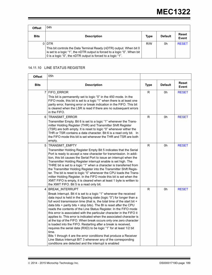
MEC1322
14.11.10 LINE STATUS REGISTER
0 DTR
This bit controls the Data Terminal Ready (nDTR) output. When bit 0 is set to a logic “1”, the nDTR output is forced to a logic “0”. When bit 0 is a logic “0”, the nDTR output is forced to a logic “1”.
R/W 0h RESET
Offset 05h
Bits Description Type DefaultReset Event
7 FIFO_ERROR
This bit is permanently set to logic “0” in the 450 mode. In the FIFO mode, this bit is set to a logic “1” when there is at least one parity error, framing error or break indication in the FIFO. This bit is cleared when the LSR is read if there are no subsequent errors in the FIFO.
R 0h RESET
6 TRANSMIT_ERROR
Transmitter Empty. Bit 6 is set to a logic “1” whenever the Trans-mitter Holding Register (THR) and Transmitter Shift Register (TSR) are both empty. It is reset to logic “0” whenever either the THR or TSR contains a data character. Bit 6 is a read only bit. In the FIFO mode this bit is set whenever the THR and TSR are both empty,
R 0h RESET
5 TRANSMIT_EMPTY
Transmitter Holding Register Empty Bit 5 indicates that the Serial Port is ready to accept a new character for transmission. In addi-tion, this bit causes the Serial Port to issue an interrupt when the Transmitter Holding Register interrupt enable is set high. The THRE bit is set to a logic “1” when a character is transferred from the Transmitter Holding Register into the Transmitter Shift Regis-ter. The bit is reset to logic “0” whenever the CPU loads the Trans-mitter Holding Register. In the FIFO mode this bit is set when the XMIT FIFO is empty, it is cleared when at least 1 byte is written to the XMIT FIFO. Bit 5 is a read only bit.
R 0h RESET
4 BREAK_INTERRUPT
Break Interrupt. Bit 4 is set to a logic “1” whenever the received data input is held in the Spacing state (logic “0”) for longer than a full word transmission time (that is, the total time of the start bit + data bits + parity bits + stop bits). The BI is reset after the CPU reads the contents of the Line Status Register. In the FIFO mode this error is associated with the particular character in the FIFO it applies to. This error is indicated when the associated character is at the top of the FIFO. When break occurs only one zero character is loaded into the FIFO. Restarting after a break is received, requires the serial data (RXD) to be logic “1” for at least 1/2 bit time. Bits 1 through 4 are the error conditions that produce a Receiver Line Status Interrupt BIT 3 whenever any of the corresponding conditions are detected and the interrupt is enabled
R 0h RESET
Offset 04h
Bits Description Type DefaultReset Event
2014 - 2015 Microchip Technology Inc. DS00001719D-page 189

MEC1322
14.11.11 MODEM STATUS REGISTER
3 FRAME_ERROR
Framing Error. Bit 3 indicates that the received character did not have a valid stop bit. Bit 3 is set to a logic “1” whenever the stop bit following the last data bit or parity bit is detected as a zero bit (Spacing level). This bit is reset to a logic “0” whenever the Line Status Register is read. In the FIFO mode this error is associated with the particular character in the FIFO it applies to. This error is indicated when the associated character is at the top of the FIFO. The Serial Port will try to resynchronize after a framing error. To do this, it assumes that the framing error was due to the next start bit, so it samples this 'start' bit twice and then takes in the 'data'.
R 0h RESET
2 PARITY ERRORParity Error. Bit 2 indicates that the received data character does not have the correct even or odd parity, as selected by the even parity select bit. This bit is set to a logic “1” upon detection of a parity error and is reset to a logic “0” whenever the Line Status Register is read. In the FIFO mode this error is associated with the particular character in the FIFO it applies to. This error is indicated when the associated character is at the top of the FIFO.
R 0h RESET
1 OVERRUN_ERROR
Overrun Error. Bit 1 indicates that data in the Receiver Buffer Reg-ister was not read before the next character was transferred into the register, thereby destroying the previous character. In FIFO mode, an overrun error will occur only when the FIFO is full and the next character has been completely received in the shift regis-ter, the character in the shift register is overwritten but not trans-ferred to the FIFO. This bit is set to a logic “1” immediately upon detection of an overrun condition, and reset whenever the Line Status Register is read.
R 0h RESET
0 DATA_READY
Data Ready. It is set to a logic ‘1’ whenever a complete incoming character has been received and transferred into the Receiver Buffer Register or the FIFO. Bit 0 is reset to a logic ‘0’ by reading all of the data in the Receive Buffer Register or the FIFO.
R 0h RESET
Offset 06h
Bits Description Type DefaultReset Event
7 DCD
This bit is the complement of the Data Carrier Detect (nDCD) input. If bit 4 of the MCR is set to logic ‘1’, this bit is equivalent to OUT2 in the MCR.
R 0h RESET
6 RI#
This bit is the complement of the Ring Indicator (nRI) input. If bit 4 of the MCR is set to logic ‘1’, this bit is equivalent to OUT1 in the MCR.
R 0h RESET
Offset 05h
Bits Description Type DefaultReset Event
DS00001719D-page 190 2014 - 2015 Microchip Technology Inc.

MEC1322
14.11.12 SCRATCHPAD REGISTER
5 DSR
This bit is the complement of the Data Set Ready (nDSR) input. If bit 4 of the MCR is set to logic ‘1’, this bit is equivalent to DTR in the MCR.
R 0h RESET
4 CTS
This bit is the complement of the Clear To Send (nCTS) input. If bit 4 of the MCR is set to logic ‘1’, this bit is equivalent to nRTS in the MCR.
R 0h RESET
3 DCD
Delta Data Carrier Detect (DDCD). Bit 3 indicates that the nDCD input to the chip has changed state. NOTE: Whenever bit 0, 1, 2, or 3 is set to a logic ‘1’, a MODEM Sta-tus Interrupt is generated.
R 0h RESET
2 RI
Trailing Edge of Ring Indicator (TERI). Bit 2 indicates that the nRI input has changed from logic ‘0’ to logic ‘1’.
R 0h RESET
1 DSR
Delta Data Set Ready (DDSR). Bit 1 indicates that the nDSR input has changed state since the last time the MSR was read.
R 0h RESET
0 CTS
Delta Clear To Send (DCTS). Bit 0 indicates that the nCTS input to the chip has changed state since the last time the MSR was read.
R 0h RESET
Note: The Modem Status Register (MSR) only provides the current state of the UART MODEM control lines inLoopback Mode. The MEC1322 does not support external connections for the MODEM Control inputs(nCTS, nDSR, nRI and nDCD) or for the four MODEM Control outputs (nDTR, nRTS, OUT1 and OUT2).
Offset 07h
Bits Description Type DefaultReset Event
7:0 SCRATCH
This 8 bit read/write register has no effect on the operation of the Serial Port. It is intended as a scratchpad register to be used by the programmer to hold data temporarily.
R/W 0h RESET
Offset 06h
Bits Description Type DefaultReset Event
2014 - 2015 Microchip Technology Inc. DS00001719D-page 191

MEC1322
15.0 EC INTERRUPT AGGREGATOR
15.1 Introduction
The EC Interrupt Aggregator works in conjunction with the processor’s interrupt interface to handle hardware interruptsand exceptions.
Exceptions are synchronous to instructions, are not maskable, and have higher priority than interrupts. All three excep-tions - reset, memory error, and instruction error - are hardwired directly to the processor. Interrupts are typically asyn-chronous and are maskable.
Interrupts classified as wake events can be recognized without a running clock, e.g., while the MEC1322 is in sleepstate.
This chapter focuses on the EC Interrupt Aggregator. Please refer to embedded controller’s documentation for moreinformation on interrupt and exception handling.
15.2 References
None
15.3 Terminology
None
15.4 Interface
FIGURE 15-1: BLOCK DIAGRAM OF EC Interrupt Aggregator
GIRQ8 Source Register
GIRQ9 Source Register
GIRQ10 Source Register
GIRQ23 Source Register
31 31 31
Interrupt Sources
AOI AOI AOI AOIMasking
BitsMasking
BitsMasking
BitsMasking
Bits
Processor
16
31
DS00001719D-page 192 2014 - 2015 Microchip Technology Inc.

MEC1322
15.4.1 SIGNAL INTERFACE
This block is not accessible from the pin interface.
15.4.2 HOST INTERFACE
The registers defined for the EC Interrupt Aggregator are only accessible by the embedded controller via the EC-OnlyRegisters.
15.5 Power, Clocks and Reset
15.5.1 BLOCK POWER DOMAIN
15.5.2 BLOCK CLOCKS
None
15.5.3 BLOCK RESET
15.6 Interrupts
This block aggregates all the interrupts targeted for the embedded controller into the Source Registers defined in Sec-tion 15.9, "EC-Only Registers," on page 202. The unmasked bits of each source register are then OR’d together androuted to the embedded controller’s interrupt interface. The name of each Source Register identifies the IRQ number ofthe interrupt port on the embedded controller.
15.7 Low Power Modes
This block always automatically adjusts to operate in the lowest power mode.
15.8 Description
The interrupt generation logic is made of 16 groups of signals, each of which consist of a Status register, a Enable reg-ister and a Result register.
The Status and Enable are latched registers. The Result register is a bit by bit AND function of the Source and Enableregisters. All the bits of the Result register are OR’ed together and AND’ed with the corresponding bit in the Block Selectregister to form the interrupt signal that is routed to the ARM interrupt controller.
The Result register bits may also be enabled to the NVIC block via the NVIC_EN bit in the Interrupt Control register.See Chapter 35.0, "EC Subsystem Registers"
Section 15.8.1 shows a representation of the interrupt structure.
TABLE 15-1: BLOCK POWER
Power Well Source Effect on Block
VCC1The EC Interrupt Aggregator block and registers operate on this single power well.
TABLE 15-2: BLOCK RESETS
Reset Name Reset Description
VCC1_RESETThis signal is used to indicate when the VCC1 logic and regis-ters in this block are reset.
2014 - 2015 Microchip Technology Inc. DS00001719D-page 193

MEC1322
FIGURE 15-2: INTERRUPT STRUCTURE
15.8.1 WAKE GENERATION
The EC Interrupt Aggregator notifies the Chip Power Management Features to wake the system when it detects a wakecapable event has occurred. This logic requires no clocks.
The interrupt sources AND’ed with the corresponding Enable bit will be OR’ed to produce a wake event
The wake up sources are identified with a “Y” in the “WAKE” column of the Bit definitions table for each IRQ’s SourceRegister.
15.8.1.1 Configuring Wake Interrupts
All GPIO inputs are wake-capable. In order for a GPIO input to wake the MEC1322 from a sleep state, the InterruptDetection field of the GPIO Pin Control Register must be set to Rising Edge Triggered, Falling Edge Triggered, or EitherEdge Triggered. If the Interrupt Detection field is set to any other value, a GPIO input will not trigger a wake interrupt.
Some of the Wake Capable Interrupts are triggered by activity on pins that are shared with a GPIO. These interrupts willonly trigger a wake if the Interrupt Detection field of the corresponding GPIO Pin Control Register is set to Rising EdgeTriggered, Falling Edge Triggered, or Either Edge Triggered.
APPLICATION NOTE: Neither LPC accesses nor JTAG debug accesses are wake capable. In order to enable LPCtransactions to MEC1322 Logical Devices while the MEC1322 is in a Sleep mode in whichthe main oscillator is shut off, just before entering sleep EC firmware must enable an interrupton the falling edge of the GPIO associated with the LFRAME# input. When responding tothis LFRAME/GPIO interrupt EC firmware should disable the LFRAME/GPIO interrupt untilfirmware determines that it is again appropriate to enter a Deep Sleep mode. Similarly, EC
SOURCE0
ENABLE0
Int source
Int enable
SOURCE1
SOURCEn
...
ENABLE1
ENABLEn
...
...
...
...
Interrupt from block
NVIC Inputs for
blocksGIRQx
Block Enable
NVIC Input for GIRQx
Bit x
...
Interrupt from block
Interrupt from block
NVIC_EN
result
To Wake Interface
...
...
DS00001719D-page 194 2014 - 2015 Microchip Technology Inc.

MEC1322
firmware must enable an interrupt on the falling edge of the GPIO associated withJTAG_CLK if JTAG debug accesses are required while the MEC1322 is in a sleep mode inwhich the main clock is turned off.
15.8.2 INTERRUPT SUMMARY
Table 15-3, "Interrupt Event Aggregator Routing Summary" summarizes the interrupts, wake capabilities and NVIC vec-tor locations.
Table 15-4, "EC Interrupt Structure" summarizes the interrupts, priorities and vector locations.
TABLE 15-3: INTERRUPT EVENT AGGREGATOR ROUTING SUMMARY
Interrupt Aggregator IRQ Aggregator BitWake Event
Aggregated NVICDirect NVIC
Interrupt
GPIO140 GIRQ8 0 Yes 57 N/A
GPIO141 GIRQ8 1
GPIO142 GIRQ8 2
GPIO143 GIRQ8 3
GPIO144 GIRQ8 4
GPIO145 GIRQ8 5
GPIO146 GIRQ8 6
GPIO147 GIRQ8 7
GPIO150 GIRQ8 8
GPIO151 GIRQ8 9
GPIO152 GIRQ8 10
GPIO153 GIRQ8 11
GPIO154 GIRQ8 12
GPIO155 GIRQ8 13
GPIO156 GIRQ8 14
GPIO157 GIRQ8 15
GPIO160 GIRQ8 16
GPIO161 GIRQ8 17
GPIO162 GIRQ8 18
GPIO163 GIRQ8 19
GPIO164 GIRQ8 20
GPIO165 GIRQ8 21
2014 - 2015 Microchip Technology Inc. DS00001719D-page 195
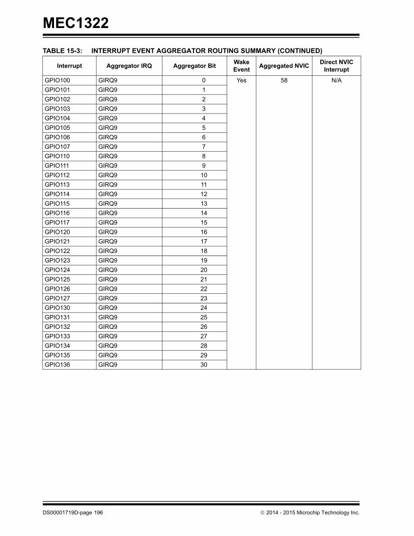
MEC1322
GPIO100 GIRQ9 0 Yes 58 N/A
GPIO101 GIRQ9 1
GPIO102 GIRQ9 2
GPIO103 GIRQ9 3
GPIO104 GIRQ9 4
GPIO105 GIRQ9 5
GPIO106 GIRQ9 6
GPIO107 GIRQ9 7
GPIO110 GIRQ9 8
GPIO111 GIRQ9 9
GPIO112 GIRQ9 10
GPIO113 GIRQ9 11
GPIO114 GIRQ9 12
GPIO115 GIRQ9 13
GPIO116 GIRQ9 14
GPIO117 GIRQ9 15
GPIO120 GIRQ9 16
GPIO121 GIRQ9 17
GPIO122 GIRQ9 18
GPIO123 GIRQ9 19
GPIO124 GIRQ9 20
GPIO125 GIRQ9 21
GPIO126 GIRQ9 22
GPIO127 GIRQ9 23
GPIO130 GIRQ9 24
GPIO131 GIRQ9 25
GPIO132 GIRQ9 26
GPIO133 GIRQ9 27
GPIO134 GIRQ9 28
GPIO135 GIRQ9 29
GPIO136 GIRQ9 30
TABLE 15-3: INTERRUPT EVENT AGGREGATOR ROUTING SUMMARY (CONTINUED)
Interrupt Aggregator IRQ Aggregator BitWake Event
Aggregated NVICDirect NVIC
Interrupt
DS00001719D-page 196 2014 - 2015 Microchip Technology Inc.

MEC1322
GPIO040 GIRQ10 0 Yes 59 N/A
GPIO041 GIRQ10 1
GPIO042 GIRQ10 2
GPIO043 GIRQ10 3
GPIO044 GIRQ10 4
GPIO045 GIRQ10 5
GPIO046 GIRQ10 6
GPIO047 GIRQ10 7
GPIO050 GIRQ10 8
GPIO051 GIRQ10 9
GPIO052 GIRQ10 10
GPIO053 GIRQ10 11
GPIO054 GIRQ10 12
GPIO055 GIRQ10 13
GPIO056 GIRQ10 14
GPIO057 GIRQ10 15
GPIO060 GIRQ10 16
GPIO061 GIRQ10 17
GPIO062 GIRQ10 18
GPIO063 GIRQ10 19
GPIO064 GIRQ10 20
GPIO065 GIRQ10 21
GPIO066 GIRQ10 22
GPIO067 GIRQ10 23
TABLE 15-3: INTERRUPT EVENT AGGREGATOR ROUTING SUMMARY (CONTINUED)
Interrupt Aggregator IRQ Aggregator BitWake Event
Aggregated NVICDirect NVIC
Interrupt
2014 - 2015 Microchip Technology Inc. DS00001719D-page 197

MEC1322
GPIO000 GIRQ11 0 Yes 60 N/A
GPIO001 GIRQ11 1
GPIO002 GIRQ11 2
GPIO003 GIRQ11 3
GPIO004 GIRQ11 4
GPIO005 GIRQ11 5
GPIO006 GIRQ11 6
GPIO007 GIRQ11 7
GPIO010 GIRQ11 8
GPIO011 GIRQ11 9
GPIO012 GIRQ11 10
GPIO013 GIRQ11 11
GPIO014 GIRQ11 12
GPIO015 GIRQ11 13
GPIO016 GIRQ11 14
GPIO017 GIRQ11 15
GPIO020 GIRQ11 16
GPIO021 GIRQ11 17
GPIO022 GIRQ11 18
GPIO023 GIRQ11 19
GPIO024 GIRQ11 20
GPIO025 GIRQ11 21
GPIO026 GIRQ11 22
GPIO027 GIRQ11 23
GPIO030 GIRQ11 24
GPIO031 GIRQ11 25
GPIO032 GIRQ11 26
GPIO033 GIRQ11 27
GPIO034 GIRQ11 28
GPIO035 GIRQ11 29
GPIO036 GIRQ11 30
I2C0 / SMB0 GIRQ12 0 No 61 0
I2C1 / SMB1 GIRQ12 1 1
I2C2 / SMB2 GIRQ12 2 2
I2C3 / SMB3 GIRQ12 3 3
I2C0_0_WK GIRQ12 4 Yes N/A
I2C0_1_WK GIRQ12 5
I2C2_0_WK GIRQ12 6
I2C1_0_WK GIRQ12 7
I2C3_0_WK GIRQ12 8
TABLE 15-3: INTERRUPT EVENT AGGREGATOR ROUTING SUMMARY (CONTINUED)
Interrupt Aggregator IRQ Aggregator BitWake Event
Aggregated NVICDirect NVIC
Interrupt
DS00001719D-page 198 2014 - 2015 Microchip Technology Inc.

MEC1322
DMA0 GIRQ13 16 No 62 4
DMA1 GIRQ13 17 5
DMA2 GIRQ13 18 6
DMA3 GIRQ13 19 7
DMA4 GIRQ13 20 8
DMA5 GIRQ13 21 9
DMA6 GIRQ13 22 10
DMA7 GIRQ13 23 11
DMA8 GIRQ13 24 81
DMA9 GIRQ13 25 82
DMA10 GIRQ13 26 83
DMA11 GIRQ13 27 84
LPC GIRQ14 2 No 63 12
UART_0 GIRQ15 0 No 64 13
Reserved GIRQ15 1 N/A
EMI_0 (IMAP) GIRQ15 2 14
Reserved GIRQ15 3 N/A
Reserved GIRQ15 4 N/A
Reserved GIRQ15 5 N/A
ACPIEC[0] IBF GIRQ15 6 15
ACPIEC[0] OBF GIRQ15 7 16
ACPIEC[1] IBF GIRQ15 8 17
ACPIEC[1] OBF GIRQ15 9 18
ACPIPM1 CTL GIRQ15 10 19
ACPIPM1 EN GIRQ15 11 20
ACPIPM1 STS GIRQ15 12 21
8042EM OBF GIRQ15 13 22
8042EM IBF GIRQ15 14 23
MAILBOX GIRQ15 15 24
MAILBOX DATA GIRQ15 16 40
PECIHOST GIRQ16 3 No 65 25
TABLE 15-3: INTERRUPT EVENT AGGREGATOR ROUTING SUMMARY (CONTINUED)
Interrupt Aggregator IRQ Aggregator BitWake Event
Aggregated NVICDirect NVIC
Interrupt
2014 - 2015 Microchip Technology Inc. DS00001719D-page 199

MEC1322
TACH_0 GIRQ17 0 No 66 26
TACH_1 GIRQ17 1 No 27
PS2_0_WK GIRQ17 2 Yes N/A
PS2_1_WK GIRQ17 3 Yes
PS2_2_WK GIRQ17 4 Yes
PS2_3_WK GIRQ17 5 Yes
BC_INT_N_WK GIRQ17 6 Yes
ADC_SNGL GIRQ17 10 No 28
ADC_RPT GIRQ17 11 No 29
MCHP Reserved GIRQ17 12 No 30
MCHP Reserved GIRQ17 13 No 31
PS2_0 GIRQ17 14 No 32
PS2_1 GIRQ17 15 No 33
PS2_2 GIRQ17 16 No 34
PS2_3 GIRQ17 17 No 35
RTC GIRQ17 18 Yes 91
RTC ALARM GIRQ17 19 Yes 92
HTIMER GIRQ17 20 Yes 38
KSC_INT GIRQ17 21 No 39
KSC_INT wake GIRQ17 22 Yes N/A
RPM_INT Stall GIRQ17 23 No 41
RPM_INT Spin GIRQ17 24 No 42
PFR_STS GIRQ17 25 No 43
PWM_WDT0 GIRQ17 26 No 44
PWM_WDT1 GIRQ17 27 No 45
PWM_WDT2 GIRQ17 28 No 46
BCM_INT Err GIRQ17 29 No 47
BCM_INT Busy GIRQ17 30 No 48
SPI0 TX GIRQ18 0 No 67 36
SPI0 RX GIRQ18 1 37
SPI1 TX GIRQ18 2 55
SPI1 RX GIRQ18 3 56
PWM_WDT3 GIRQ18 4 85
MCHP Reserved GIRQ18 5 86
MCHP Reserved GIRQ18 6 87
MCHP Reserved GIRQ18 7 88
MCHP Reserved GIRQ18 8 89
MCHP Reserved GIRQ18 9 90
VCC_PWRGD GIRQ19 0 Yes 68 N/A
LRESET# GIRQ19 1
GPIO200 GIRQ20 0 Yes 69 N/A
GPIO201 GIRQ20 1
GPIO202 GIRQ20 2
GPIO203 GIRQ20 3
TABLE 15-3: INTERRUPT EVENT AGGREGATOR ROUTING SUMMARY (CONTINUED)
Interrupt Aggregator IRQ Aggregator BitWake Event
Aggregated NVICDirect NVIC
Interrupt
DS00001719D-page 200 2014 - 2015 Microchip Technology Inc.

MEC1322
GPIO204 GIRQ20 4
N/A GIRQ20 5
GPIO206 GIRQ20 6
N/A GIRQ20 7
GPIO210 GIRQ20 8
GPIO211 GIRQ20 9
TIMER_16_0 GIRQ23 0 No 72 49
TIMER_16_1 GIRQ23 1 50
TIMER_16_2 GIRQ23 2 51
TIMER_16_3 GIRQ23 3 52
TIMER_32_0 GIRQ23 4 53
TIMER_32_1 GIRQ23 5 54
TABLE 15-4: EC INTERRUPT STRUCTURE
Vector NameLink
RegisterPriority(Default)
RelativePriority
ByteOffset
0 Reset - High H1 00h
1 Memory Error ILINK2 High H2 08h
2 Instruction Error ILINK2 High H3 10h
3 IRQ3-Reserved ILINK1 level 1 (low) L27 18h
4 IRQ4-Reserved ILINK1 level 1 (low) L26 20h
5 IRQ5-Reserved ILINK1 level 1 (low) L25 28h
6 IRQ6-Reserved ILINK2 level 2 (mid) M2 30h
7 IRQ7-Reserved ILINK2 level 2 (mid) M1 38h
8 IRQ8 ILINK1 level 1 (low) L24 40h
9 IRQ9 ILINK1 level 1 (low) L23 48h
10 IRQ10 ILINK1 level 1 (low) L22 50h
11 IRQ11 ILINK1 level 1 (low) L21 58h
12 IRQ12 ILINK1 level 1 (low) L20 60h
13 IRQ13 ILINK1 level 1 (low) L19 68h
14 IRQ14 ILINK1 level 1 (low) L18 70h
15 IRQ15 ILINK1 level 1 (low) L17 78h
16 IRQ16 ILINK1 level 1 (low) L16 80h
17 IRQ17 ILINK1 level 1 (low) L15 88h
18 IRQ18 ILINK1 level 1 (low) L14 90h
19 IRQ19 ILINK1 level 1 (low) L13 98h
20 IRQ20 ILINK1 level 1 (low) L12 A0h
21 IRQ21 ILINK1 level 1 (low) L11 A8h
22 IRQ22 ILINK1 level 1 (low) L10 B0h
23 IRQ23 ILINK1 level 1 (low) L9 B8h
24 IRQ24 ILINK1 level 1 (low) L8 C0h
25 IRQ25 ILINK1 level 1 (low) L7 C8h
26 IRQ26 ILINK1 level 1 (low) L6 D0h
TABLE 15-3: INTERRUPT EVENT AGGREGATOR ROUTING SUMMARY (CONTINUED)
Interrupt Aggregator IRQ Aggregator BitWake Event
Aggregated NVICDirect NVIC
Interrupt
2014 - 2015 Microchip Technology Inc. DS00001719D-page 201

MEC1322
15.8.3 DISABLING INTERRUPTS
The Block Enable Clear Register and Block Enable Set Register should not be used for disabling and enabling interruptsfor software operations i.e., critical sections. The ARM enable disable mechanisms should be used.
15.9 EC-Only Registers
The configuration registers listed in EC-Only Register Summary table are for a single instance of the EC Interrupt Aggre-gator. The addresses of each register listed in the summary table are defined as a relative offset to the host “BeginAddress” defined in the EC-Only Register Base Address Table.
Note 15-1 The Begin Address indicates the location of the first register accessable at offset 00h in the InterruptAggregator EC-Only address space.
27 IRQ27 ILINK1 level 1 (low) L5 D8h
28 IRQ28 ILINK1 level 1 (low) L4 E0h
29 IRQ29 ILINK1 level 1 (low) L3 E8h
30 IRQ30 ILINK1 level 1 (low) L2 F0h
31 IRQ31 ILINK1 level 1 (low) L1 F8h
Note: IRQ Vector 31 is the highest L1 Priority
TABLE 15-5: EC-ONLY REGISTER ADDRESS RANGE TABLE
Instance NameInstance Number Host Address Space
Begin Address (Note 15-1)
Interrupt Aggregator 0 EC 32-bit internal address space
4000_C000h
TABLE 15-6: EC-ONLY REGISTER SUMMARY
Offset Register Name
00h GIRQ8 Source Register
04h GIRQ8 Enable Set Register
08h GIRQ8 Result Register
0Ch GIRQ8 Enable Clear Register
14h GIRQ9 Source Register
18h GIRQ9 Enable Set Register
1Ch GIRQ9 Result Register
20h GIRQ9 Enable Clear Register
28h GIRQ10 Source Register
2Ch GIRQ10 Enable Set Register
30h GIRQ10 Result Register
34h GIRQ10 Enable Clear Register
3Ch GIRQ11 Source Register
40h GIRQ11 Enable Set Register
44h GIRQ11 Result Register
48h GIRQ11 Enable Clear Register
TABLE 15-4: EC INTERRUPT STRUCTURE (CONTINUED)
Vector NameLink
RegisterPriority(Default)
RelativePriority
ByteOffset
DS00001719D-page 202 2014 - 2015 Microchip Technology Inc.

MEC1322
50h GIRQ12 Source Register
54h GIRQ12 Enable Set Register
58h GIRQ12 Result Register
5Ch GIRQ12 Enable Clear Register
64h GIRQ13 Source Register
68h GIRQ13 Enable Set Register
6Ch GIRQ13 Result Register
70h GIRQ13 Enable Clear Register
78h GIRQ14 Source Register
7Ch GIRQ14 Enable Set Register
80h GIRQ14 Result Register
84h GIRQ14 Enable Clear Register
8Ch GIRQ15 Source Register
90h GIRQ15 Enable Set Register
94h GIRQ15 Result Register
98h GIRQ15 Enable Clear Register
A0h GIRQ16 Source Register
A4h GIRQ16 Enable Set Register
A8h GIRQ16 Result Register
ACh GIRQ16 Enable Clear Register
B4h GIRQ17 Source Register
B8h GIRQ17 Enable Set Register
BCh GIRQ17 Result Register
C0h GIRQ17 Enable Clear Register
C8h GIRQ18 Source Register
CCh GIRQ18 Enable Set Register
D0h GIRQ18 Result Register
D4h GIRQ18 Enable Clear Register
DCh GIRQ19 Source Register
E0h GIRQ19 Enable Set Register
E4h GIRQ19 Result Register
E8h GIRQ19 Enable Clear Register
F0h GIRQ20 Source Register
F4h GIRQ20 Enable Set Register
F8h GIRQ20 Result Register
FCh GIRQ20 Enable Clear Register
104h GIRQ21 Source Register
108h GIRQ21 Enable Set Register
10Ch GIRQ21 Result Register
110h GIRQ21 Enable Clear Register
118h GIRQ22 Source Register
11Ch GIRQ22 Enable Set Register
120h GIRQ22 Result Register
124h GIRQ22 Enable Clear Register
TABLE 15-6: EC-ONLY REGISTER SUMMARY (CONTINUED)
Offset Register Name
2014 - 2015 Microchip Technology Inc. DS00001719D-page 203

MEC1322
All of the GIRQx Source, Enable, and Result registers have the same format. The following tables define the genericformat for each of these registers. The bit definitions are defined in the sections that follow.
The R/WC bits are sticky status bits indicating the state of interrupt source before the interrupt enable bit.
GIRQ Enable Set [31:0]
Each GIRQx bit can be individually enabled to assert an interrupt event.
0= Writing a zero has no effect.
1= Writing a one will enable respective GIRQx.
Reading always returns the current value of the GIRQx ENABLE bit. The state of the GIRQx ENABLE bit is determinedby the corresponding GIRQx Enable Set bit and the GIRQx Enable Clear bit. (0=disabled, 1-enabled)
12Ch GIRQ23 Source Register
130h GIRQ23 Enable Set Register
134h GIRQ23 Result Register
138h GIRQ23 Enable Clear Register
200h Block Enable Set Register
204h Block Enable Clear Register
208h Block IRQ Vector Register
Note: The behavior of the enable bit controlled by the GIRQx Enable Set and GIRQx Enable Clear Registers, theGIRQx Source bit, and the GIRQx Result bit are illustrated in Section 15.8.1, "WAKE Generation," onpage 194.
TABLE 15-7: GIRQX SOURCE REGISTER
Offset - 32-bit Size
PowerVCC1 0000_0000h VCC1_RESET
Default
Bit D31 D30 D29 • • • D2 D1 D0
Type R R/WC except for reserved bits, which are R
Bit Name Reserved See Tables in the following subsections
TABLE 15-8: GIRQX ENABLE SET REGISTER
Offset - 32-bit Size
POWERVCC1 0000_0000h VCC1_RESET
Default
BIT D31 D30 D29 • • • D2 D1 D0
TYPE R R/WS except for reserved bits, which are R
BIT NAME Reserved See Tables in the following subsections
TABLE 15-6: EC-ONLY REGISTER SUMMARY (CONTINUED)
Offset Register Name
DS00001719D-page 204 2014 - 2015 Microchip Technology Inc.

MEC1322
GIRQx Interrupt Result
Bits D30 down to D0 are defined in the following subsections reflect the state of the GIRQx interrupt source after theenable bit. The GIRQx result bits are OR’d together to generate the IRQx vector.
Bit D31
Bit D31 is hard-coded to ‘1’.
GIRQx Enable Clear[31:0]
Each GIRQx bit can be individually disabled to assert an interrupt event.
0= Writing a zero has no effect.
1= Writing a one will disable respective GIRQx.
Reading always returns the current value of the GIRQx ENABLE bit. The state of the GIRQx ENABLE bit is determinedby the corresponding GIRQx Enable Set bit and the GIRQx Enable Clear bit. (0=disabled, 1-enabled)
15.9.1 GIRQ8
TABLE 15-9: GIRQX RESULT REGISTER
Offset - 32-bit EC Size
POWERVCC1 8000_0000h VCC1_RESET
Default
BIT D31 D30 D29 • • • D2 D1 D0
TYPE R R
BIT NAME ‘1’ See Tables in the following subsections
TABLE 15-10: GIRQX ENABLE CLEAR REGISTER
Offset - 32-bit Size
POWERVCC1 0000_0000h VCC1_RESET
Default
BIT D31 D30 D29 • • • D2 D1 D0
TYPE R R/WC except for reserved bits, which are R
BIT NAME Reserved See Tables in the following subsections
TABLE 15-11: BIT DEFINITIONS FOR GIRQ8 SOURCE, ENABLE, AND RESULT REGISTERS
BitBlock Instance
NameSource Name Wake Source Description
[7:0] GPIO[147:140] GPIO_Event Y Bits[0:7] are controlled by the GPIO_Events gener-ated by GPIO140 through GPIO147, respectively.
The GPIO Interface can generate an interrupt source event on a high level, low level, rising edge and fall-ing edge, as configured by the Interrupt Detection (int_det) bits in the Pin Control Register associated with the GPIO signal function.
2014 - 2015 Microchip Technology Inc. DS00001719D-page 205

MEC1322
15.9.2 GIRQ9
[15:8] GPIO[157:150] GPIO_Event Y Bits[8:15] are controlled by the GPIO_Events gener-ated by GPIO150 through GPIO157, respectively.
The GPIO Interface can generate an interrupt source event on a high level, low level, rising edge and fall-ing edge, as configured by the Interrupt Detection (int_det) bits in the Pin Control Register associated with the GPIO signal function.
[21:16] GPIO[165:160] GPIO_Event Y Bits[16:21] are controlled by the GPIO_Events gen-erated by GPIO160 through GPIO165, respectively.
The GPIO Interface can generate an interrupt source event on a high level, low level, rising edge and fall-ing edge, as configured by the Interrupt Detection (int_det) bits in the Pin Control Register associated with the GPIO signal function.
[30:22] Reserved Reserved N Reserved
31 n/a n/a N See Table 15-7, "GIRQx Source Register", Table 15-8, "GIRQx Enable Set Register", Table 15-10, "GIRQx Enable Clear Register", and Table 15-9, "GIRQx Result Register" for a definition of this bit for the Source, Enable, and Result registers.
TABLE 15-12: BIT DEFINITIONS FOR GIRQ9 SOURCE, ENABLE, AND RESULT REGISTERS
BitBlock Instance
NameSource Name Wake Source Description
[7:0] GPIO[107:100] GPIO_Event Y Bits[0:7] are controlled by the GPIO_Events generated by GPIO100 through GPIO107, respectively.
The GPIO Interface can generate an interrupt source event on a high level, low level, rising edge and falling edge, as configured by the Interrupt Detection (int_det) bits in the Pin Control Register associated with the GPIO signal function.
[15:8] GPIO[117:110] GPIO_Event Y Bits[8:15] are controlled by the GPIO_Events gener-ated by GPIO110 through GPIO117, respectively.
The GPIO Interface can generate an interrupt source event on a high level, low level, rising edge and falling edge, as configured by the Interrupt Detection (int_det) bits in the Pin Control Register associated with the GPIO signal function.
[23:16] GPIO[127:120] GPIO_Event Y Bits[16:23] are controlled by the GPIO_Events gener-ated by GPIO120 through GPIO127, respectively.
The GPIO Interface can generate an interrupt source event on a high level, low level, rising edge and falling edge, as configured by the Interrupt Detection (int_det) bits in the Pin Control Register associated with the GPIO signal function.
TABLE 15-11: BIT DEFINITIONS FOR GIRQ8 SOURCE, ENABLE, AND RESULT REGISTERS
BitBlock Instance
NameSource Name Wake Source Description
DS00001719D-page 206 2014 - 2015 Microchip Technology Inc.
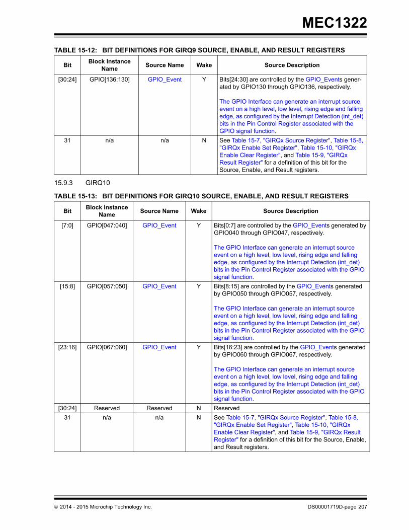
MEC1322
15.9.3 GIRQ10
[30:24] GPIO[136:130] GPIO_Event Y Bits[24:30] are controlled by the GPIO_Events gener-ated by GPIO130 through GPIO136, respectively.
The GPIO Interface can generate an interrupt source event on a high level, low level, rising edge and falling edge, as configured by the Interrupt Detection (int_det) bits in the Pin Control Register associated with the GPIO signal function.
31 n/a n/a N See Table 15-7, "GIRQx Source Register", Table 15-8, "GIRQx Enable Set Register", Table 15-10, "GIRQx Enable Clear Register", and Table 15-9, "GIRQx Result Register" for a definition of this bit for the Source, Enable, and Result registers.
TABLE 15-13: BIT DEFINITIONS FOR GIRQ10 SOURCE, ENABLE, AND RESULT REGISTERS
BitBlock Instance
NameSource Name Wake Source Description
[7:0] GPIO[047:040] GPIO_Event Y Bits[0:7] are controlled by the GPIO_Events generated by GPIO040 through GPIO047, respectively.
The GPIO Interface can generate an interrupt source event on a high level, low level, rising edge and falling edge, as configured by the Interrupt Detection (int_det) bits in the Pin Control Register associated with the GPIO signal function.
[15:8] GPIO[057:050] GPIO_Event Y Bits[8:15] are controlled by the GPIO_Events generated by GPIO050 through GPIO057, respectively.
The GPIO Interface can generate an interrupt source event on a high level, low level, rising edge and falling edge, as configured by the Interrupt Detection (int_det) bits in the Pin Control Register associated with the GPIO signal function.
[23:16] GPIO[067:060] GPIO_Event Y Bits[16:23] are controlled by the GPIO_Events generated by GPIO060 through GPIO067, respectively.
The GPIO Interface can generate an interrupt source event on a high level, low level, rising edge and falling edge, as configured by the Interrupt Detection (int_det) bits in the Pin Control Register associated with the GPIO signal function.
[30:24] Reserved Reserved N Reserved
31 n/a n/a N See Table 15-7, "GIRQx Source Register", Table 15-8, "GIRQx Enable Set Register", Table 15-10, "GIRQx Enable Clear Register", and Table 15-9, "GIRQx Result Register" for a definition of this bit for the Source, Enable, and Result registers.
TABLE 15-12: BIT DEFINITIONS FOR GIRQ9 SOURCE, ENABLE, AND RESULT REGISTERS
BitBlock Instance
NameSource Name Wake Source Description
2014 - 2015 Microchip Technology Inc. DS00001719D-page 207

MEC1322
15.9.4 GIRQ11
15.9.5 GIRQ12
TABLE 15-14: BIT DEFINITIONS FOR GIRQ11 SOURCE, ENABLE, AND RESULT REGISTERS
BitBlock Instance
NameSource Name Wake Source Description
[7:0] GPIO[007:000] GPIO_Event Y Bits[0:7] are controlled by the GPIO_Events generated by GPIO000 through GPIO007, respectively.
The GPIO Interface can generate an interrupt source event on a high level, low level, rising edge and falling edge, as configured by the Interrupt Detection (int_det) bits in the Pin Control Register associated with the GPIO signal function.
[15:8] GPIO[017:010] GPIO_Event Y Bits[8:15] are controlled by the GPIO_Events generated by GPIO010 through GPIO017, respectively.
The GPIO Interface can generate an interrupt source event on a high level, low level, rising edge and falling edge, as configured by the Interrupt Detection (int_det) bits in the Pin Control Register associated with the GPIO signal function.
[23:16] GPIO[027:020] GPIO_Event Y Bits[16:23] are controlled by the GPIO_Events generated by GPIO020 through GPIO027, respectively.
The GPIO Interface can generate an interrupt source event on a high level, low level, rising edge and falling edge, as configured by the Interrupt Detection (int_det) bits in the Pin Control Register associated with the GPIO signal function.
[30:24] GPIO[036:030] GPIO_Event Y Bits[24:30] are controlled by the GPIO_Events generated by GPIO030 through GPIO036, respectively.
The GPIO Interface can generate an interrupt source event on a high level, low level, rising edge and falling edge, as configured by the Interrupt Detection (int_det) bits in the Pin Control Register associated with the GPIO signal function.
31 n/a n/a N See Table 15-7, "GIRQx Source Register", Table 15-8, "GIRQx Enable Set Register", Table 15-10, "GIRQx Enable Clear Register", and Table 15-9, "GIRQx Result Register" for a definition of this bit for the Source, Enable, and Result registers.
TABLE 15-15: BIT DEFINITIONS FOR GIRQ12 SOURCE, ENABLE, AND RESULT REGISTERS
BitBlock Instance
NameSource Name Wake Source Description
0 I2C0 / SMB0 SMB N I2C/SMBus controller 0 interrupt. This interrupt is signaled when the I2C/SMBus controller 0 asserts its interrupt request.
1 I2C1 / SMB1 SMB N I2C/SMBus controller 1 interrupt. This interrupt is signaled when the I2C/SMBus controller 1 asserts its interrupt request.
2 I2C2 / SMB2 SMB N I2C/SMBus controller 2 interrupt. This interrupt is signaled when the I2C/SMBus controller 2 asserts its interrupt request.
DS00001719D-page 208 2014 - 2015 Microchip Technology Inc.
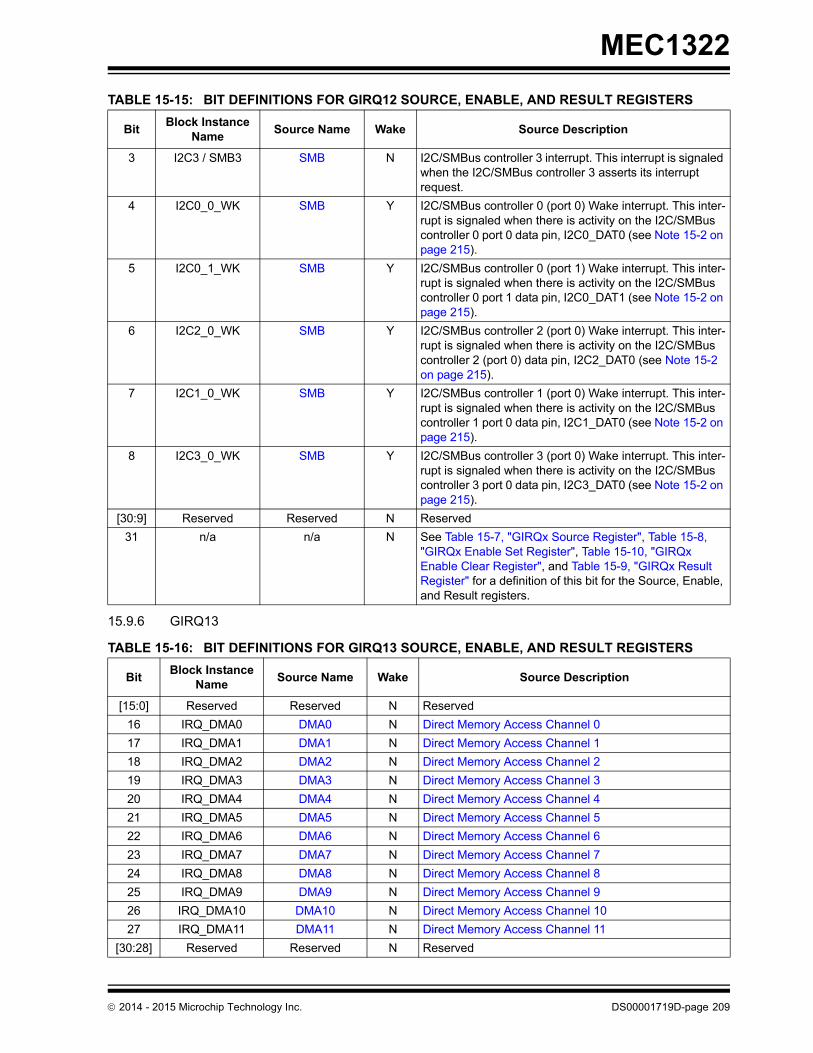
MEC1322
15.9.6 GIRQ13
3 I2C3 / SMB3 SMB N I2C/SMBus controller 3 interrupt. This interrupt is signaled when the I2C/SMBus controller 3 asserts its interrupt request.
4 I2C0_0_WK SMB Y I2C/SMBus controller 0 (port 0) Wake interrupt. This inter-rupt is signaled when there is activity on the I2C/SMBus controller 0 port 0 data pin, I2C0_DAT0 (see Note 15-2 on page 215).
5 I2C0_1_WK SMB Y I2C/SMBus controller 0 (port 1) Wake interrupt. This inter-rupt is signaled when there is activity on the I2C/SMBus controller 0 port 1 data pin, I2C0_DAT1 (see Note 15-2 on page 215).
6 I2C2_0_WK SMB Y I2C/SMBus controller 2 (port 0) Wake interrupt. This inter-rupt is signaled when there is activity on the I2C/SMBus controller 2 (port 0) data pin, I2C2_DAT0 (see Note 15-2 on page 215).
7 I2C1_0_WK SMB Y I2C/SMBus controller 1 (port 0) Wake interrupt. This inter-rupt is signaled when there is activity on the I2C/SMBus controller 1 port 0 data pin, I2C1_DAT0 (see Note 15-2 on page 215).
8 I2C3_0_WK SMB Y I2C/SMBus controller 3 (port 0) Wake interrupt. This inter-rupt is signaled when there is activity on the I2C/SMBus controller 3 port 0 data pin, I2C3_DAT0 (see Note 15-2 on page 215).
[30:9] Reserved Reserved N Reserved
31 n/a n/a N See Table 15-7, "GIRQx Source Register", Table 15-8, "GIRQx Enable Set Register", Table 15-10, "GIRQx Enable Clear Register", and Table 15-9, "GIRQx Result Register" for a definition of this bit for the Source, Enable, and Result registers.
TABLE 15-16: BIT DEFINITIONS FOR GIRQ13 SOURCE, ENABLE, AND RESULT REGISTERS
BitBlock Instance
NameSource Name Wake Source Description
[15:0] Reserved Reserved N Reserved
16 IRQ_DMA0 DMA0 N Direct Memory Access Channel 0
17 IRQ_DMA1 DMA1 N Direct Memory Access Channel 1
18 IRQ_DMA2 DMA2 N Direct Memory Access Channel 2
19 IRQ_DMA3 DMA3 N Direct Memory Access Channel 3
20 IRQ_DMA4 DMA4 N Direct Memory Access Channel 4
21 IRQ_DMA5 DMA5 N Direct Memory Access Channel 5
22 IRQ_DMA6 DMA6 N Direct Memory Access Channel 6
23 IRQ_DMA7 DMA7 N Direct Memory Access Channel 7
24 IRQ_DMA8 DMA8 N Direct Memory Access Channel 8
25 IRQ_DMA9 DMA9 N Direct Memory Access Channel 9
26 IRQ_DMA10 DMA10 N Direct Memory Access Channel 10
27 IRQ_DMA11 DMA11 N Direct Memory Access Channel 11
[30:28] Reserved Reserved N Reserved
TABLE 15-15: BIT DEFINITIONS FOR GIRQ12 SOURCE, ENABLE, AND RESULT REGISTERS
BitBlock Instance
NameSource Name Wake Source Description
2014 - 2015 Microchip Technology Inc. DS00001719D-page 209

MEC1322
15.9.7 GIRQ14
15.9.8 GIRQ15
31 n/a n/a N See Table 15-7, "GIRQx Source Register", Table 15-8, "GIRQx Enable Set Register", Table 15-10, "GIRQx Enable Clear Register", and Table 15-9, "GIRQx Result Register" for a definition of this bit for the Source, Enable, and Result registers.
TABLE 15-17: BIT DEFINITIONS FOR GIRQ14 SOURCE, ENABLE, AND RESULT REGISTERS
BitBlock Instance
NameSource Name Wake Source Description
[1:0] Reserved Reserved N Reserved
2 IRQ_LPC LPC_INTER-NAL_ERR
N The LPC_INTERNAL_ERR event is sourced by bit D0 of the Host Bus Error Register.
[30:3] Reserved Reserved N Reserved
31 n/a n/a N See Table 15-7, "GIRQx Source Register", Table 15-8, "GIRQx Enable Set Register", Table 15-10, "GIRQx Enable Clear Register", and Table 15-9, "GIRQx Result Register" for a definition of this bit for the Source, Enable, and Result registers.
TABLE 15-18: BIT DEFINITIONS FOR GIRQ15 SOURCE, ENABLE, AND RESULT REGISTERS
BitBlock Instance
NameSource Name Wake Source Description
0 UART_0 UART N The UART interrupt event output indicates if an interrupt is pending. See Table 14-13, “Interrupt Control Table,” on page 186.
1 Reserved Reserved N Reserved
2 EMI_0 Host-to-EC N Communication event notifying the embedded controller that the host has written to the Host-to-EC register.
5:3 Reserved Reserved N Reserved
6 ACPI_EC[0] IBF EC_IBF N EC_IBF interrupt is asserted when the IBF in the STATUS EC-Register is set to ‘1’.
7 ACPI_EC[0] OBF EC_OBF N EC_OBF interrupt is asserted when the OBF in the STA-TUS EC-Register is cleared to ‘0’.
8 ACPI_EC[1] IBF EC_IBF N EC_IBF interrupt is asserted when the IBF in the STATUS EC-Register is set to ‘1’.
9 ACPI_EC[1] OBF EC_OBF N EC_OBF interrupt is asserted when the OBF in the STA-TUS EC-Register is cleared to ‘0’.
10 ACPI_PM1_CTL ACPIPM1_CTL N PM1_CTL2 written by Host
11 ACPIPM1 EN ACPIPM1_EN N PM1_EN2 written by Host
12 ACPIPM1 STS ACPIPM1_STS N PM1_STS2 written by Host
13 8042EM OBF 8042EM_OBF N Interrupt generated by the host reading either data or aux data from the data register
14 8042EM IBF 8042EM_IBF N Interrupt generated by the host writing either data or com-mand to the data register
15 MBX MBX Host-to-EC N Interrupt generated for HOST-to-EC events for writes to the HOST-to-EC Mailbox Register
TABLE 15-16: BIT DEFINITIONS FOR GIRQ13 SOURCE, ENABLE, AND RESULT REGISTERS
BitBlock Instance
NameSource Name Wake Source Description
DS00001719D-page 210 2014 - 2015 Microchip Technology Inc.

MEC1322
15.9.9 GIRQ16
15.9.10 GIRQ17
16 MBX_DATA MBX_DATA N Interrupt generated for Host writes to Mailbox Data Regis-ter
[30:17] Reserved Reserved N Reserved
31 n/a n/a N See Table 15-7, "GIRQx Source Register", Table 15-8, "GIRQx Enable Set Register", Table 15-10, "GIRQx Enable Clear Register", and Table 15-9, "GIRQx Result Register" for a definition of this bit for the Source, Enable, and Result registers.
TABLE 15-19: BIT DEFINITIONS FOR GIRQ16 SOURCE, ENABLE, AND RESULT REGISTERS
BitBlock Instance
NameSource Name Wake Source Description
[2:0] Reserved Reserved N Reserved
3 PECIHOST PECIHOST N PECI Host
[30:4] Reserved Reserved N Reserved
31 n/a n/a N See Table 15-7, "GIRQx Source Register", Table 15-8, "GIRQx Enable Set Register", Table 15-10, "GIRQx Enable Clear Register", and Table 15-9, "GIRQx Result Register" for a definition of this bit for the Source, Enable, and Result registers.
TABLE 15-20: BIT DEFINITIONS FOR GIRQ17 SOURCE, ENABLE, AND RESULT REGISTERS
BitBlock Instance
NameSource Name Wake Source Description
0 IRQ_TACH0 TACH N This internal signal is generated from the OR’d result of the status events, as defined in the TACHx Status Regis-ter..
1 IRQ_TACH1 TACH N This internal signal is generated from the OR’d result of the status events, as defined in the TACHx Status Regis-ter.
2 PS2_0_WK PS2_DAT0 pin Y PS2_0 Start Detect from pin signal PS2_DAT0 (see Note 15-2 on page 215).
3 PS2_1_WK PS2_DAT1 pin Y PS2_1 Start Detect from pin signal PS2_DAT1 (see Note 15-2 on page 215).
4 PS2_2_WK PS2_DAT2 pin Y PS2_2 Start Detect from pin signal PS2_DAT2 (see Note 15-2 on page 215).
5 PS2_3_WK PS2_DAT3 pin Y PS2_3 Start Detect from pin signal PS2_DAT3 (see Note 15-2 on page 215).
6 BC_INT_N_WK BC_LINK Y Interrupt from the BC_LINK Companion BC_INT# pin (see Note 15-2 on page 215).
[9:7] Reserved Reserved N Reserved
10 ADC_SNGL ADC_Single_Int N Interrupt signal from ADC controller to EC for Single-Sample ADC conversion
11 ADC_RPT ADC_Repeat_Int N Interrupt signal from ADC controller to EC for Repeated ADC conversion
12 MCHP Reserved MCHP Reserved N MCHP Reserved
TABLE 15-18: BIT DEFINITIONS FOR GIRQ15 SOURCE, ENABLE, AND RESULT REGISTERS
BitBlock Instance
NameSource Name Wake Source Description
2014 - 2015 Microchip Technology Inc. DS00001719D-page 211

MEC1322
15.9.11 GIRQ18
13 MCHP Reserved MCHP Reserved N MCHP Reserved
14 PS2_0 PS2 ACT N PS2_0 Activity Interrupt from PS/2 Block
15 PS2_1 PS2 ACT N PS2_1 Activity Interrupt from PS/2 Block
16 PS2_2 PS2 ACT N PS2_2 Activity Interrupt from PS/2 Block
17 PS2_3 PS2 ACT N PS2_3 Activity Interrupt from PS/2 Block
18 RTC RTC Y RTC Interrupt
19 RTC ALARM RTC ALARM Y RTC Alarm Interrupt
20 HTIMER HTIMER Y Signal indicating that the hibernation timer is enabled and has expired.
21 KEYSCAN KSC_INT N Keyboard Scan Interface runtime interrupt
22 KEYSCAN wake KSC_INT_WAKE Y Keyboard Scan Interface wake interrupt
23 RPM_INT Stall Fan Stall Status Interrupt
N RPM-PWM Interface DRIVE_FAIL & FAN_SPIN indica-tion
24 RPM_INT Spin Fan Fail/Spin Sta-tus Interrupt
N RPM-PWM Interface SPIN indication
25 PFR_Status PFR_Status N Power-Fail and Reset Status Register events (VBAT POR and WDT).
26 PWM_WDT[0] PWM_WDT N PWM watchdog time out interrupt from Blinking/Breathing PWM block
27 PWM_WDT[1] PWM_WDT N PWM watchdog time out interrupt from Blinking/Breathing PWM block
28 PWM_WDT[2] PWM_WDT N PWM watchdog time out interrupt from Blinking/Breathing PWM block
29 BCM_ERR BCM_INT Err N BC_LINK Master Error Flag Interrupt
30 BCM_BUSY_-CLR
BCM_INT Busy N BC_LINK Master Busy Clear Flag Interrupt
31 n/a n/a N See Table 15-7, "GIRQx Source Register", Table 15-8, "GIRQx Enable Set Register", Table 15-10, "GIRQx Enable Clear Register", and Table 15-9, "GIRQx Result Register" for a definition of this bit for the Source, Enable, and Result registers.
TABLE 15-21: BIT DEFINITIONS FOR GIRQ18 SOURCE, ENABLE, AND RESULT REGISTERS
BitBlock Instance
NameSource Name Wake Source Description
0 SPI0 TX TXBE_STS N SPI controller 0 Interrupt output to EC driven by TXBE status bit
1 SPI0 RX RXBF_STS N SPI controller 0 Interrupt output to EC driven by RXBE status bit
2 SPI1 TX TXBE_STS N SPI controller 1 Interrupt output to EC driven by TXBE status bit
3 SPI1 RX RXBF_STS N SPI controller 1 Interrupt output to EC driven by RXBE status bit
4 PWM_WDT[3] PWM_WDT N PWM watchdog time out interrupt from Blinking/Breathing PWM block
5 MCHP Reserved MCHP Reserved N MCHP Reserved
TABLE 15-20: BIT DEFINITIONS FOR GIRQ17 SOURCE, ENABLE, AND RESULT REGISTERS
BitBlock Instance
NameSource Name Wake Source Description
DS00001719D-page 212 2014 - 2015 Microchip Technology Inc.

MEC1322
15.9.12 GIRQ19
15.9.13 GIRQ20
6 MCHP Reserved MCHP Reserved N MCHP Reserved
7 MCHP Reserved MCHP Reserved N MCHP Reserved
8 MCHP Reserved MCHP Reserved N MCHP Reserved
9 MCHP Reserved MCHP Reserved N MCHP Reserved
[30:10] Reserved Reserved N Reserved
31 n/a n/a N See Table 15-7, "GIRQx Source Register", Table 15-8, "GIRQx Enable Set Register", Table 15-10, "GIRQx Enable Clear Register", and Table 15-9, "GIRQx Result Register" for a definition of this bit for the Source, Enable, and Result registers.
TABLE 15-22: BIT DEFINITIONS FOR GIRQ19 SOURCE, ENABLE, AND RESULT REGISTERS
BitBlock Instance
NameSource Name Wake Source Description
0 VCC_PWRGD VCC_PWRGD Y VCC_PWRGD interrupt from pin (see Note 15-2 on page 215).
1 LRESET# LRESET# Y LRESET# interrupt from pin (see Note 15-2 on page 215).
[30:2] Reserved Reserved N Reserved
31 n/a n/a N See Table 15-7, "GIRQx Source Register", Table 15-8, "GIRQx Enable Set Register", Table 15-10, "GIRQx Enable Clear Register", and Table 15-9, "GIRQx Result Register" for a definition of this bit for the Source, Enable, and Result registers.
TABLE 15-23: BIT DEFINITIONS FOR GIRQ20 SOURCE, ENABLE, AND RESULT REGISTERS
BitBlock Instance
NameSource Name Wake Source Description
[4:0] GPIO[204:200] GPIO_Event Y Bits[0:4] are controlled by the GPIO_Events generated by GPIO200 through GPIO204, respectively.
The GPIO Interface can generate an interrupt source event on a high level, low level, rising edge and falling edge, as configured by the Interrupt Detection (int_det) bits in the Pin Control Register associated with the GPIO signal function.
5 Reserved Reserved N Reserved
6 GPIO206 GPIO_Event Y Bit 6 is controlled by the GPIO_Events generated by GPIO206.
The GPIO Interface can generate an interrupt source event on a high level, low level, rising edge and falling edge, as configured by the Interrupt Detection (int_det) bits in the Pin Control Register associated with the GPIO signal function.
7 Reserved Reserved N Reserved
TABLE 15-21: BIT DEFINITIONS FOR GIRQ18 SOURCE, ENABLE, AND RESULT REGISTERS
BitBlock Instance
NameSource Name Wake Source Description
2014 - 2015 Microchip Technology Inc. DS00001719D-page 213

MEC1322
15.9.14 GIRQ21
15.9.15 GIRQ22
15.9.16 GIRQ23
[9:8] GPIO[211:210] GPIO_Event Y Bits[8:9] are controlled by the GPIO_Events generated by GPIO210 through GPIO211, respectively.
The GPIO Interface can generate an interrupt source event on a high level, low level, rising edge and falling edge, as configured by the Interrupt Detection (int_det) bits in the Pin Control Register associated with the GPIO signal function.
[11:10] MCHP Reserved MCHP Reserved N/A MCHP Reserved
[30:12] Reserved Reserved N Reserved
31 n/a n/a N See Table 15-7, "GIRQx Source Register", Table 15-8, "GIRQx Enable Set Register", Table 15-10, "GIRQx Enable Clear Register", and Table 15-9, "GIRQx Result Register" for a definition of this bit for the Source, Enable, and Result registers.
TABLE 15-24: BIT DEFINITIONS FOR GIRQ21 SOURCE, ENABLE, AND RESULT REGISTERS
BitBlock Instance
NameSource Name Wake Source Description
[1:0] MCHP Reserved n/a n/a n/a
[30:2] Reserved Reserved N Reserved
31 n/a n/a N See Table 15-7, "GIRQx Source Register", Table 15-8, "GIRQx Enable Set Register", Table 15-10, "GIRQx Enable Clear Register", and Table 15-9, "GIRQx Result Register" for a definition of this bit for the Source, Enable, and Result registers.
TABLE 15-25: BIT DEFINITIONS FOR GIRQ22 SOURCE, ENABLE, AND RESULT REGISTERS
BitBlock Instance
NameSource Name Wake Source Description
[30:0] Reserved Reserved N Reserved
31 n/a n/a N See Table 15-7, "GIRQx Source Register", Table 15-8, "GIRQx Enable Set Register", Table 15-10, "GIRQx Enable Clear Register", and Table 15-9, "GIRQx Result Register" for a definition of this bit for the Source, Enable, and Result registers.
TABLE 15-26: BIT DEFINITIONS FOR GIRQ23 SOURCE, ENABLE, AND RESULT REGISTERS
BitBlock Instance
NameSource Name Wake Source Description
0 16-bit Timer_0 TIMER_32_x N This interrupt event fires when a 32-bit timer x reaches its limit. This event is sourced by the tEVENT_INTERRUPT status bit if enabled.
TABLE 15-23: BIT DEFINITIONS FOR GIRQ20 SOURCE, ENABLE, AND RESULT REGISTERS
BitBlock Instance
NameSource Name Wake Source Description
DS00001719D-page 214 2014 - 2015 Microchip Technology Inc.

MEC1322
Note 15-2 All wakeup interrupts associated with pins must be configured as falling edge interrupts through theassociated GPIO control register.
15.9.17 BLOCK ENABLE SET REGISTER
IRQ Vector Enable Set [31:0]
Each IRQ Vector can be individually enabled to assert an interrupt event to the EC.
0= Writing a zero has no effect.
1 16-bit Timer_1 TIMER_32_x N This interrupt event fires when a 32-bit timer x reaches its limit. This event is sourced by the tEVENT_INTERRUPT status bit if enabled.
2 16-bit Timer_2 TIMER_32_x N This interrupt event fires when a 32-bit timer x reaches its limit. This event is sourced by the tEVENT_INTERRUPT status bit if enabled.
3 16-bit Timer_3 TIMER_32_x N This interrupt event fires when a 32-bit timer x reaches its limit. This event is sourced by the tEVENT_INTERRUPT status bit if enabled.
4 32-bit Timer_0 TIMER_32_x N This interrupt event fires when a 32-bit timer x reaches its limit. This event is sourced by the tEVENT_INTERRUPT status bit if enabled.
5 32-bit Timer_1 TIMER_32_x N This interrupt event fires when a 32-bit timer x reaches its limit. This event is sourced by the tEVENT_INTERRUPT status bit if enabled.
[30:6] Reserved Reserved N Reserved
31 n/a n/a N See Table 15-7, "GIRQx Source Register", Table 15-8, "GIRQx Enable Set Register", Table 15-10, "GIRQx Enable Clear Register", and Table 15-9, "GIRQx Result Register" for a definition of this bit for the Source, Enable, and Result registers.
Offset 200h 32-bit Size
POWERVCC1 0000_0000h VCC1_RESET
Default
BIT D31 D30 D29 D28 D27 D26 D25 D24
TYPE R R R R R R R R
BIT NAME Reserved
BIT D23 D22 D21 D20 D19 D18 D17 D16
TYPE R/WS R/WS R/WS R/WS R/WS R/WS R/WS R/WS
BIT NAME IRQ Vector Enable Set [23:16]
BIT D15 D14 D13 D12 D11 D10 D9 D8
TYPE R/WS R/WS R/WS R/WS R/WS R/WS R/WS R/WS
BIT NAME IRQ Vector Enable Set [15:8]
BIT D7 D6 D5 D4 D3 D2 D1 D0
TYPE R R R R R R R R
BIT NAME Reserved
TABLE 15-26: BIT DEFINITIONS FOR GIRQ23 SOURCE, ENABLE, AND RESULT REGISTERS
BitBlock Instance
NameSource Name Wake Source Description
2014 - 2015 Microchip Technology Inc. DS00001719D-page 215

MEC1322
1= Writing a one will enable respective IRQi.
Reading always returns the current value of the IRQ i VECTOR ENABLE bit. The state of the IRQ i VECTOR ENABLEbit is determined by the corresponding IRQ i Vector Enable Set bit and the IRQ i Vector Enable Clear bit. (0=disabled,1-enabled)
15.9.18 BLOCK ENABLE CLEAR REGISTER
IRQ Vector Enable Clear[31:0]
Each IRQ Vector can be individually disabled to assert an interrupt event to the EC.
0= Writing a zero has no effect.
1= Writing a one will disable respective IRQi vector.
Reading always returns the current value of the IRQ i VECTOR ENABLE bit. The state of the IRQ i VECTOR ENABLEbit is determined by the corresponding IRQ i Vector Enable Set bit and the IRQ i Vector Enable Clear bit. (0=disabled,1-enabled)
15.9.19 BLOCK IRQ VECTOR REGISTER
Offset 204h 32-bit Size
POWERVCC1 0000_0000h VCC1_RESET
Default
BIT D31 D30 D29 D28 D27 D26 D25 D24
TYPE R R R R R R R R
BIT NAME Reserved
BIT D23 D22 D21 D20 D19 D18 D17 D16
TYPE R/WC R/WC R/WC R/WC R/WC R/WC R/WC R/WC
BIT NAME IRQ Vector Enable Clear [23:16]
BIT D15 D14 D13 D12 D11 D10 D9 D8
TYPE R/WC R/WC R/WC R/WC R/WC R/WC R/WC R/WC
BIT NAME IRQ Vector Enable Clear [15:8]
BIT D7 D6 D5 D4 D3 D2 D1 D0
TYPE R R R R R R R R
BIT NAME Reserved
Offset 208h 32-bit Size
POWERVCC1 0000_0000h VCC1_RESET
Default
BIT D31 D30 D29 D28 D27 D26 D25 D24
TYPE R R R R R R R R
BIT NAME Reserved
BIT D23 D22 D21 D20 D19 D18 D17 D16
TYPE R R R R R R R R
DS00001719D-page 216 2014 - 2015 Microchip Technology Inc.

MEC1322
IRQ Vector [31:0]
Each read only bit reflects the current state of the IRQ i vector to the EC.
BIT NAME IRQ Vector [23:16]
BIT D15 D14 D13 D12 D11 D10 D9 D8
TYPE R R R R R R R R
BIT NAME IRQ Vector [15:8]
BIT D7 D6 D5 D4 D3 D2 D1 D0
TYPE R R R R R R R R
BIT NAME Reserved
Note: If the IRQ i vector is disabled via the Block Enable Clear Register the corresponding IRQ i vector to the ECis forced to 0. If the IRQ i vector is enabled, the corresponding IRQ i vector to the EC represents the currentstatus of the IRQ event.
2014 - 2015 Microchip Technology Inc. DS00001719D-page 217

MEC1322
16.0 WATCHDOG TIMER (WDT)
16.1 Introduction
The function of the Watchdog Timer is to provide a mechanism to detect if the internal embedded controller has failed.
When enabled, the Watchdog Timer (WDT) circuit will generate a WDT Event if the user program fails to reload the WDTwithin a specified length of time known as the WDT Interval.
16.2 References
No references have been cited for this chapter.
16.3 Terminology
There is no terminology defined for this chapter.
16.4 Interface
This block is designed to be accessed internally via a registered host interface or externally via the signal interface.
16.5 Host Interface
The registers defined for the Watchdog Timer (WDT) are accessible by the embedded controller as indicated in Section16.8, "EC-Only Registers". All registers accesses are synchronized to the host clock and complete immediately. Regis-ter reads/writes are not delayed by the 32KHz_Clk.
FIGURE 16-1: I/O DIAGRAM OF BLOCK
Watchdog Timer (WDT)
Clock Inputs
WDT Event
Resets
Host Interface
DS00001719D-page 218 2014 - 2015 Microchip Technology Inc.

MEC1322
16.6 Power, Clocks and Reset
This section defines the Power, Clock, and Reset parameters of the block.
16.6.1 POWER DOMAINS
16.6.2 CLOCK INPUTS
16.6.3 RESETS
16.7 Description
16.7.1 WDT OPERATION
16.7.1.1 WDT Activation Mechanism
The WDT is activated by the following sequence of operations during normal operation:
1. Load the WDT Load Register with the count value.
2. Set the WDT Enable bit in the WDT Control Register.
The WDT Activation Mechanism starts the WDT decrementing counter.
16.7.1.2 WDT Deactivation Mechanism
The WDT is deactivated by the clearing the WDT Enable bit in the WDT Control Register. The WDT Deactivation Mech-anism places the WDT in a low power state in which clock are gated and the counter stops decrementing.
16.7.1.3 WDT Reload Mechanism
The WDT must be reloaded within periods that are shorter than the programmed watchdog interval; otherwise, the WDTwill underflow and a WDT Event will be generated and the WDT Status bit will be set in the WDT Control Register. It isthe responsibility of the user program to continually execute code which reloads the watchdog timer, causing the counterto be reloaded
There are three methods of reloading the WDT: a write to the WDT Load Register, a write to the WDT Kick Register, orWDT event.
TABLE 16-1: POWER SOURCES
Name Description
VCC1 The logic and registers implemented in this block reside on this singlepower well.
TABLE 16-2: CLOCK INPUTS
Name Description
32KHz_Clk The 32KHz_Clk clock input is the clock source to the Watchdog Timer functional logic, including the counter.
TABLE 16-3: RESET SIGNALS
Name Description
VCC1_RESET Power on Reset to the block. This signal resets all the register and logic in this block to its default state.
TABLE 16-4: RESET OUTPUT EVENT
Source Description
WDT Event Pulse generated when WDT expires. This signal is used to reset the embedded controller and its subsystem.
The event is cleared after an VCC1_RESET.
2014 - 2015 Microchip Technology Inc. DS00001719D-page 219
MEC1322
16.7.1.4 WDT Interval
The WDT Interval is the time it takes for the WDT to decrements from the WDT Load Register value to 0000h. The WDTCount Register value takes 33/32KHz_Clk seconds (ex. 33/32.768 KHz = 1.007ms) to decrement by 1 count.
16.8 EC-Only Registers
The registers listed in the EC-Only Register Summary table are for a single instance of the Watchdog Timer (WDT). Theaddresses of each register listed in this table are defined as a relative offset to the host “Base Address” defined in theEC-Only Register Base Address Table.
The Base Address indicates where the first register can be accessed in a particular address space for a block instance.
16.8.1 WDT LOAD REGISTER
16.8.2 WDT CONTROL REGISTER
TABLE 16-5: EC-ONLY REGISTER BASE ADDRESS TABLE
Block InstanceInstance Number Host Address Space Base Address
WDT 0 EC 32-bit internal address space
4000_0400h
TABLE 16-6: EC-ONLY REGISTER SUMMARY
Offset Register Name (Mnemonic)
00h WDT Load Register
04h WDT Control Register
08h WDT Kick Register
0Ch WDT Count Register
Offset 00h
Bits Description Type DefaultReset Event
15:0 WDT Load
Writing this field reloads the Watch Dog Timer counter.
R/W Fh VCC1_RESET
Offset 04h
Bits Description Type DefaultReset Event
7:2 RESERVED R - -
1 WDT Status
WDT_RST is set by hardware if the last reset of MEC1322 was caused by an underflow of the WDT. See Section 16.7.1.3, "WDT Reload Mechanism," on page 219 for more information.
This bit must be cleared by the EC firmware writing a ‘1’ to this bit. Writing a ‘0’ to this bit has no effect.
R/WC 0b VCC1_RESET
DS00001719D-page 220 2014 - 2015 Microchip Technology Inc.
MEC1322
16.8.3 WDT KICK REGISTER
16.8.4 WDT COUNT REGISTER
0 WDT Enable
In WDT Operation, the WDT is activated by the sequence of opera-tions defined in Section 16.7.1.1, "WDT Activation Mechanism" and deactivated by the sequence of operations defined in Section 16.7.1.2, "WDT Deactivation Mechanism".
0 = block disabled1 = block enabled
Note: The default of the WDT is inactive.
R/W 0b VCC1_RESET
Offset 08h
Bits Description Type DefaultReset Event
7:0 Kick
The WDT Kick Register is a strobe. Reads of the WDT Kick Register return 0. Writes to the WDT Kick Register cause the WDT to reload the WDT Load Register value and start decrementing when the WDT Enable bit in the WDT Control Register is set to ‘1’. When the WDT Enable bit in the WDT Control Register is cleared to ‘0’, writes to the WDT Kick Register have no effect.
W n/a VCC1_RESET
Offset 0Ch
Bits Description Type DefaultReset Event
15:0 WDT Count
This read-only register provide the current WDT count.
R Fh VCC1_RESET
Offset 04h
Bits Description Type DefaultReset Event
2014 - 2015 Microchip Technology Inc. DS00001719D-page 221

MEC1322
17.0 BASIC TIMER
17.1 Introduction
This timer block offers a simple mechanism for firmware to maintain a time base. This timer may be instantiated as 16bits or 32 bits. The name of the timer instance indicates the size of the timer.
17.2 Interface
This block is designed to be accessed externally via the pin interface and internally via a registered host interface.
17.3 Signal Description
There are no external signals for this block.
17.4 Host Interface
The embedded controller may access this block via the registers defined in Section 17.9, "EC-Only Registers," onpage 224.
17.5 Power, Clocks and Reset
This section defines the Power, Clock, and Reset parameters of the block.
FIGURE 17-1: I/O DIAGRAM OF BLOCK
Basic Timer
Signal Description
Interrupts
Host Interface
Clock Inputs
Resets
DS00001719D-page 222 2014 - 2015 Microchip Technology Inc.

MEC1322
17.5.1 POWER DOMAINS
17.5.2 CLOCK INPUTS
17.5.3 RESETS
17.6 Interrupts
17.7 Low Power Modes
The Basic Timer may be put into a low power state by the chip’s Power, Clocks, and Reset (PCR) circuitry. This blockis only be permitted to enter low power modes when the block is not active.
The sleep state of this timer is as follows:
• Asleep while the block is not Enabled
• Asleep while the block is not running (start inactive).
• Asleep while the block is halted (even if running).
The block is active while start is active.
TABLE 17-1: POWER SOURCES
Name Description
VCC1 The timer control logic and registers are all implemented on this single power domain.
TABLE 17-2: CLOCK INPUTS
Name Description
48 MHz Ring Oscillator This is the clock source to the timer logic. The Pre-scaler may be used to adjust the minimum resolution per bit of the counter.
TABLE 17-3: RESET SIGNALS
Name Description
VCC1_RESET This reset signal, which is an input to this block, resets all the logic and registers to their initial default state.
Soft Reset This reset signal, which is created by this block, resets all the logic and registers to their initial default state. This reset is generated by the block when the SOFT_RESET bit is set in the Timer Control Register register.
Timer_Reset This reset signal, which is created by this block, is asserted when either the VCC1_RESET or the Soft Reset signal is asserted. The VCC1_RE-SET and Soft Reset signals are OR’d together to create this signal.
TABLE 17-4: EC INTERRUPTS
Source Description
TIMER_16_x This interrupt event fires when a 16-bit timer x reaches its limit. This event is sourced by the EVENT_INTERRUPT status bit if enabled.
TIMER_32_x This interrupt event fires when a 32-bit timer x reaches its limit. This event is sourced by the tEVENT_INTERRUPT status bit if enabled.
2014 - 2015 Microchip Technology Inc. DS00001719D-page 223
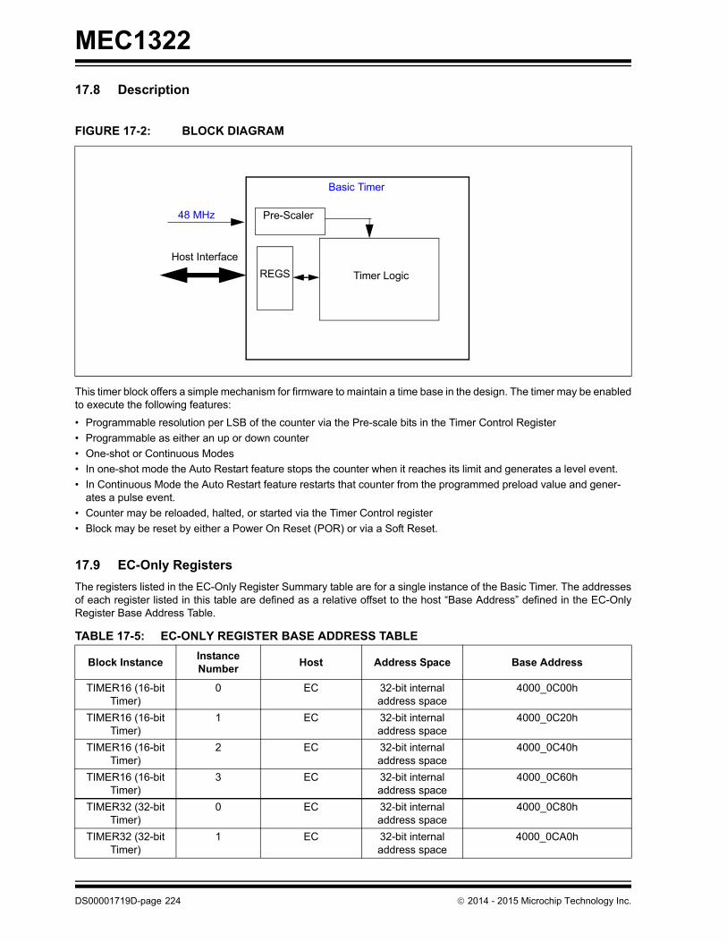
MEC1322
17.8 Description
This timer block offers a simple mechanism for firmware to maintain a time base in the design. The timer may be enabledto execute the following features:
• Programmable resolution per LSB of the counter via the Pre-scale bits in the Timer Control Register
• Programmable as either an up or down counter
• One-shot or Continuous Modes
• In one-shot mode the Auto Restart feature stops the counter when it reaches its limit and generates a level event.
• In Continuous Mode the Auto Restart feature restarts that counter from the programmed preload value and gener-ates a pulse event.
• Counter may be reloaded, halted, or started via the Timer Control register
• Block may be reset by either a Power On Reset (POR) or via a Soft Reset.
17.9 EC-Only Registers
The registers listed in the EC-Only Register Summary table are for a single instance of the Basic Timer. The addressesof each register listed in this table are defined as a relative offset to the host “Base Address” defined in the EC-OnlyRegister Base Address Table.
FIGURE 17-2: BLOCK DIAGRAM
TABLE 17-5: EC-ONLY REGISTER BASE ADDRESS TABLE
Block InstanceInstance Number
Host Address Space Base Address
TIMER16 (16-bit Timer)
0 EC 32-bit internal address space
4000_0C00h
TIMER16 (16-bit Timer)
1 EC 32-bit internal address space
4000_0C20h
TIMER16 (16-bit Timer)
2 EC 32-bit internal address space
4000_0C40h
TIMER16 (16-bit Timer)
3 EC 32-bit internal address space
4000_0C60h
TIMER32 (32-bit Timer)
0 EC 32-bit internal address space
4000_0C80h
TIMER32 (32-bit Timer)
1 EC 32-bit internal address space
4000_0CA0h
Host Interface
Basic Timer
REGS Timer Logic
Pre-Scaler48 MHz
DS00001719D-page 224 2014 - 2015 Microchip Technology Inc.
MEC1322
The Base Address indicates where the first register can be accessed in a particular address space for a block instance.
17.9.1 TIMER COUNT REGISTER
17.9.2 TIMER PRELOAD REGISTER
17.9.3 TIMER STATUS REGISTER
TABLE 17-6: RUNTIME REGISTER SUMMARY
Offset Register Name
00h Timer Count Register
04h Timer Preload Register
08h Timer Status Register
0Ch Timer Int Enable Register
10h Timer Control Register
Offset 00h
Bits Description Type DefaultReset Event
31:0 COUNTER
This is the value of the Timer counter. This is updated by Hardware but may be set by Firmware. If it is set while the Hardware Timer is operating, functionality can not be maintained. When read, it is buff-ered so single byte reads will be able to catch the full 4 byte register without it changing.
The size of the Counter is indicated by the instance name. Bits 0 to (size-1) are r/w counter bits. Bits 31 down to size are reserved. Reads return 0 and writes have no effect.
R/W 0h Tim-er_Reset
Offset 04h
Bits Description Type DefaultReset Event
31:0 PRE_LOAD
This is the value of the Timer pre-load for the counter. This is used by H/W when the counter is to be restarted automatically; this will become the new value of the counter upon restart.
The size of the Pre-Load value is the same as the size of the counter. The size of the Counter is indicated by the instance name. Bits 0 to (size-1) are r/w pre-load bits. Bits 31 down to size are reserved. Reads return 0 and writes have no effect.
R/W 0h Tim-er_Reset
Offset 08h
Bits Description Type DefaultReset Event
31:0 Reserved R - -
0 EVENT_INTERRUPT
This is the interrupt status that fires when the timer reaches its limit. This may be level or a self clearing signal cycle pulse, based on the AUTO_RESTART bit in the Timer Control Register. If the timer is set to automatically restart, it will provide a pulse, otherwise a level is provided.
R/WC 0h Tim-er_Reset
2014 - 2015 Microchip Technology Inc. DS00001719D-page 225

MEC1322
17.9.4 TIMER INT ENABLE REGISTER
17.9.5 TIMER CONTROL REGISTER
Offset 0Ch
Bits Description Type DefaultReset Event
31:0 Reserved R - -
0 EVENT_INTERRUPT_ENABLE
This is the interrupt enable for the status EVENT_INTERRUPT bit in the Timer Status Register
R/W 0h Tim-er_Reset
Offset 10h
Bits Description Type DefaultReset Event
31:16 PRE_SCALE
This is used to divide down the system clock through clock enables to lower the power consumption of the block and allow slow timers.Updating this value during operation may result in erroneous clock enable pulses until the clock divider restarts.The number of clocks per clock enable pulse is (Value + 1); a setting of 0 runs at the full clock speed, while a setting of 1 runs at half speed.
R/W 0h Tim-er_Reset
15:8 Reserved R - -
7 HALT
This is a halt bit. This will halt the timer as long as it is active. Once the halt is inactive, the timer will start from where it left off.
1=Timer is halted. It stops counting. The clock divider will also be reset.
0=Timer runs normally
R/W 0h Tim-er_Reset
6 RELOAD
This bit reloads the counter without interrupting it operation. This will not function if the timer has already completed (when the START bit in this register is ‘0’). This is used to periodically prevent the timer from firing when an event occurs. Usage while the timer is off may result in erroneous behavior.
R/W 0h Tim-er_Reset
DS00001719D-page 226 2014 - 2015 Microchip Technology Inc.

MEC1322
5 START
This bit triggers the timer counter. The counter will operate until it hits its terminating condition. This will clear this bit. It should be noted that when operating in restart mode, there is no terminating condition for the counter, so this bit will never clear. Clearing this bit will halt the timer counter.
Setting this bit will:
• Reset the clock divider counter.
• Enable the clock divider counter.
• Start the timer counter.
• Clear all interrupts.
Clearing this bit will:
• Disable the clock divider counter.
• Stop the timer counter.
R/W 0h Tim-er_Reset
4 SOFT_RESET
This is a soft reset.This is self clearing 1 cycle after it is written.
WO 0h Tim-er_Reset
3 AUTO_RESTART
This will select the action taken upon completing a count.
1=The counter will automatically restart the count, using the contentsof the Timer Preload Register to load the Timer Count RegisterThe interrupt will be set in edge mode
0=The counter will simply enter a done state and wait for further con-trol inputs. The interrupt will be set in level mode.
R/W 0h Tim-er_Reset
2 COUNT_UP
This selects the counter direction.
When the counter in incrementing the counter will saturate and trig-ger the event when it reaches all F’s. When the counter is decre-menting the counter will saturate when it reaches 0h.
1=The counter will increment0=The counter will decrement
R/W 0h Tim-er_Reset
1 Reserved R - -
0 ENABLE
This enables the block for operation.
1=This block will function normally0=This block will gate its clock and go into its lowest power state
R/W 0h Tim-er_Reset
Offset 10h
Bits Description Type DefaultReset Event
2014 - 2015 Microchip Technology Inc. DS00001719D-page 227

MEC1322
18.0 HIBERNATION TIMER
18.1 Introduction
The Hibernation Timer can generate a wake event to the Embedded Controller (EC) when it is in a hibernation mode.This block supports wake events up to 2 hours in duration. The timer is a 16-bit binary count-down timer that can beprogrammed in 30.5µs and 0.125 second increments for period ranges of 30.5µs to 2s or 0.125s to 136.5 minutes,respectively. Writing a non-zero value to this register starts the counter from that value. A wake-up interrupt is generatedwhen the count reaches zero.
18.2 References
No references have been cited for this chapter
18.3 Terminology
No terms have been cited for this chapter.
18.4 Interface
This block is an IP block designed to be incorporated into a chip. It is designed to be accessed externally via the pininterface and internally via a registered host interface. The following diagram illustrates the various interfaces to theblock.
18.5 Signal Description
There are no external signals for this block.
FIGURE 18-1: HIBERNATION TIMER INTERFACE DIAGRAM
Hibernation Timer
Signal DescriptionClock Inputs
Interrupts
Resets
Host Interface
DS00001719D-page 228 2014 - 2015 Microchip Technology Inc.

MEC1322
18.6 Host Interface
The registers defined for the Hibernation Timer are accessible by the various hosts as indicated in Section 18.10, "EC-Only Registers".
18.7 Power, Clocks and Reset
This section defines the Power, Clock, and Reset parameters of the block.
18.7.1 POWER DOMAINS
18.7.2 CLOCK INPUTS
18.7.3 RESETS
18.8 Interrupts
This section defines the interrupt Interface signals routed to the chip interrupt aggregator.
Each instance of the Hibernation Timer in the MEC1322 can be used to generate interrupts and wake-up events whenthe timer decrements to zero. The Hibernation Timer interrupt is are routed to the HTIMER bit in the GIRQ17 SourceRegister.
18.9 Low Power Modes
The Hibernation Timer may be put into a low power state by the chip Power, Clocks, and Reset (PCR) circuitry.
The timer operates off of the 32KHz_Clk, and therefore will operate normally when 48 MHz Ring Oscillator is stopped.
The sleep enable inputs have no effect on the Hibernation Timer and the clock required outputs are only asserted duringregister read/write cycles for as long as necessary to propagate updates to the block core.
18.10 EC-Only Registers
The registers listed in the EC-Only Register Summary table are for a single instance of the Hibernation Timer. Theaddresses of each register listed in this table are defined as a relative offset to the host “Base Address” defined in theEC-Only Register Base Address Table.
TABLE 18-1: POWER SOURCES
Name Description
VCC1 The timer control logic and registers are all implemented on this single power domain.
TABLE 18-2: CLOCK INPUTS
Name Description
32KHz_Clk This is the clock source to the timer logic. The Pre-scaler may be used to adjust the minimum resolution per bit of the counter.
if the main oscillator is stopped then an external 32.768kHz clock sourcemust be active for the Hibernation Timer to continue to operate.
TABLE 18-3: RESET SIGNALS
Name Description
VCC1_RESET This reset signal, which is an input to this block, resets all the logic and registers to their initial default state.
TABLE 18-4: INTERRUPT INTERFACE SIGNAL DESCRIPTION TABLE
Name Direction Description
HTIMER Output Signal indicating that the timer is enabled and decrements to 0. This signal is used to generate an Hibernation Timer interrupt event.
2014 - 2015 Microchip Technology Inc. DS00001719D-page 229

MEC1322
The Base Address indicates where the first register can be accessed in a particular address space for a block instance.
18.10.1 HTIMER PRELOAD REGISTER
18.10.2 HTIMER CONTROL REGISTER
18.10.3 HTIMER COUNT REGISTER
TABLE 18-5: EC-ONLY REGISTER BASE ADDRESS TABLE
Block InstanceInstance Number
Host Address Space Base Address
Hibernation Timer 0 EC 32-bit internal address space
4000_9800h
TABLE 18-6: HIBERNATION TIMER SUMMARY
Offset Register Name
00h HTimer Preload Register
04h HTimer Control Register
08h HTimer Count Register
Offset 00h
Bits Description Type DefaultReset Event
15:0 HT_PRELOAD
This register is used to set the Hibernation Timer Preload value. Writing this register to a non-zero value resets the down counter to start counting down from this programmed value. Writing this regis-ter to 0000h disables the hibernation counter. The resolution of this timer is determined by the CTRL bit in the HTimer Control Register.Writes to the HTimer Control Register are completed with an EC bus cycle.
R/W 000h VCC1_RESET
Offset 04h
Bits Description Type DefaultReset Event
15:1 Reserved R - -
0 CTRL
1= The Hibernation Timer has a resolution of 0.125s per LSB, whichyields a maximum time in excess of 2 hours.
0= The Hibernation Timer has a resolution of 30.5µs per LSB, whichyields a maximum time of ~2seconds.
R 0000h VCC1_RESET
Offset 08h
Bits Description Type DefaultReset Event
15:0 COUNT
The current state of the Hibernation Timer.
R 0000h VCC1_RESET
DS00001719D-page 230 2014 - 2015 Microchip Technology Inc.

MEC1322
19.0 RTC WITH DATE AND DST ADJUSTMENT
19.1 Introduction
This block provides the capabilities of an industry-standard 146818B Real-Time Clock module, without CMOS RAM.Enhancements to this architecture include:
• Industry standard Day of Month Alarm field, allowing for monthly alarms
• Configurable, automatic Daylight Savings adjustment
• Week Alarm for periodic interrupts and wakes based on Day of Week
• System Wake capability on interrupts.
19.2 References
1. Motorola 146818B Data Sheet, available on-line
2. Intel Lynx Point PCH EDS specification
19.3 Terminology
Time and Date Registers:
This is the set of registers that are automatically counted by hardware every 1 second while the block is enabled to runand to update. These registers are: Seconds, Minutes, Hours, Day of Week, Day of Month, Month, and Year.
19.4 Interface
This block’s connections are entirely internal to the chip.
FIGURE 19-1: I/O DIAGRAM OF BLOCK
RTC With Date and DST Adjust-ment
Signal DescriptionClocks
Interrupts
Host Interface
Resets
2014 - 2015 Microchip Technology Inc. DS00001719D-page 231

MEC1322
19.5 Signal Description
There are no external signals.
19.6 Host Interface
The registers defined for the RTC With Date and DST Adjustment are accessible by the host and EC.
19.7 Power, Clocks and Resets
This section defines the Power, Clock, and Reset parameters of the block.
19.7.1 POWER DOMAINS
19.7.2 CLOCKS
19.7.3 RESETS
19.8 Interrupts
TABLE 19-1: POWER SOURCES
Name Description
VBAT This power well sources all of the internal registers and logic in this block.
VCC1 This power well sources only bus communication. The block continues to operate internally while this rail is down.
TABLE 19-2: CLOCKS
Name Description
32KHz_Clk This 32KHz clock input drives all internal logic, and will be present at all times that the VBAT well is powered.
TABLE 19-3: RESET SIGNALS
Name Description
VBAT_POR This reset signal is used in the RTC_RST signal to reset all of the registers and logic in this block. It directly resets the Soft Reset bit in the RTC Control Register.
RTC_RST This reset signal resets all of the registers and logic in this block, except for the Soft Reset bit in the RTC Control Register. It is triggered by VBAT_POR, but can also be triggered by a Soft Reset from the RTC Control Register.
VCC1_RESET This reset signal is used to inhibit the bus communication logic, and isolates this block from VCC1 powered circuitry on-chip. Otherwise it has no effect on the internal state.
TABLE 19-4: SYSTEM INTERRUPTS
Source Description
RTC This interrupt source for the SIRQ logic is generated when any of the fol-lowing events occur:
• Update complete. This is triggered, at 1-second intervals, when the Time register updates have completed
• Alarm. This is triggered when the alarm value matches the current time (and date, if used)
• Periodic. This is triggered at the chosen programmable rate
DS00001719D-page 232 2014 - 2015 Microchip Technology Inc.

MEC1322
19.9 Low Power Modes
The RTC has no low-power modes. It runs continuously while the VBAT well is powered.
19.10 Description
This block provides the capabilities of an industry-standard 146818B Real-Time Clock module, excluding the CMOSRAM and the SQW output. See the following registers, which represent enhancements to this architecture. Theseenhancements are listed below.
See the Date Alarm field of Register D for a Day of Month qualifier for alarms.
See the Week Alarm Register for a Day of Week qualifier for alarms.
See the registers Daylight Savings Forward Register and Daylight Savings Backward Register for setting up hands-offDaylight Savings adjustments.
See the RTC Control Register for enhanced control over the block’s operations.
19.11 Runtime Registers
The addresses of each register listed in this table are defined as a relative offset to the host “Base Address” defined inRuntime Register Base Address Table.
The Base Address indicates where the first register can be accessed in a particular address space for a block instance.Add the register’s Offset to this value to obtain the direct address of the register.
TABLE 19-5: EC INTERRUPTS
Source Description
RTC This interrupt is signaled to the Interrupt Aggregator when any of the fol-lowing events occur:
• Update complete. This is triggered, at 1-second intervals, when the Time register updates have completed
• Alarm. This is triggered when the alarm value matches the current time (and date, if used)
• Periodic. This is triggered at the chosen programmable rate
RTC ALARM This wake interrupt is signaled to the Interrupt Aggregator when an Alarm event occurs.
TABLE 19-6: RUNTIME REGISTER BASE ADDRESS TABLE
Block InstanceInstance Number
Host Address Space Base Address
RTC 0 LPC I/O Programmed BAR
0 EC 32-bit internal Address Space
400F_2C00h
TABLE 19-7: RUNTIME REGISTER SUMMARY
Offset Register Name (Mnemonic)
00h Seconds Register
01h Seconds Alarm Register
02h Minutes Register
03h Minutes Alarm Register
04h Hours Register
05h Hours Alarm Register
06h Day of Week Register
07h Day of Month Register
08h Month Register
2014 - 2015 Microchip Technology Inc. DS00001719D-page 233

MEC1322
19.11.1 SECONDS REGISTER
19.11.2 SECONDS ALARM REGISTER
09h Year Register
0Ah Register A
0Bh Register B
0Ch Register C
0Dh Register D
0Eh (reserved)
0Fh (reserved)
10h RTC Control Register
14h Week Alarm Register
18h Daylight Savings Forward Register
1Ch Daylight Savings Backward Register
20h MCHP Reserved
Note: This extended register set occupies offsets that have historically been used as CMOS RAM. Code portedto use this block should be examined to ensure that it does not assume that RAM exists in this block.
Offset 00h
Bits Description Type DefaultReset Event
7:0 SECONDS
Displays the number of seconds past the current minute, in the range 0--59. Presentation may be selected as binary or BCD, depending on the DM bit in Register B. Values written must also use the format defined by the current setting of the DM bit.
R/W 00h RTC_RST
Offset 01h
Bits Description Type DefaultReset Event
7:0 SECONDS_ALARM
Holds a match value, compared against the Seconds Register to trig-ger the Alarm event. Values written to this register must use the for-mat defined by the current setting of the DM bit in Register B. A value of 11xxxxxxb written to this register makes it don’t-care (always matching).
R/W 00h RTC_RST
TABLE 19-7: RUNTIME REGISTER SUMMARY (CONTINUED)
Offset Register Name (Mnemonic)
DS00001719D-page 234 2014 - 2015 Microchip Technology Inc.
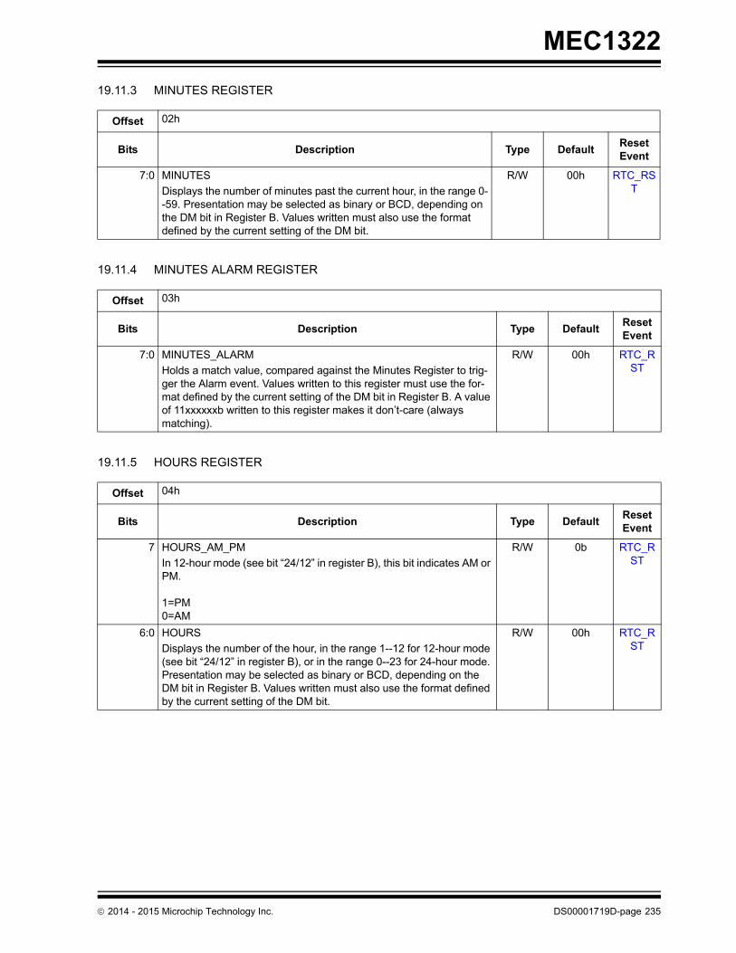
MEC1322
19.11.3 MINUTES REGISTER
19.11.4 MINUTES ALARM REGISTER
19.11.5 HOURS REGISTER
Offset 02h
Bits Description Type DefaultReset Event
7:0 MINUTES
Displays the number of minutes past the current hour, in the range 0--59. Presentation may be selected as binary or BCD, depending on the DM bit in Register B. Values written must also use the format defined by the current setting of the DM bit.
R/W 00h RTC_RST
Offset 03h
Bits Description Type DefaultReset Event
7:0 MINUTES_ALARM
Holds a match value, compared against the Minutes Register to trig-ger the Alarm event. Values written to this register must use the for-mat defined by the current setting of the DM bit in Register B. A value of 11xxxxxxb written to this register makes it don’t-care (always matching).
R/W 00h RTC_RST
Offset 04h
Bits Description Type DefaultReset Event
7 HOURS_AM_PM
In 12-hour mode (see bit “24/12” in register B), this bit indicates AM or PM.
1=PM0=AM
R/W 0b RTC_RST
6:0 HOURS
Displays the number of the hour, in the range 1--12 for 12-hour mode (see bit “24/12” in register B), or in the range 0--23 for 24-hour mode. Presentation may be selected as binary or BCD, depending on the DM bit in Register B. Values written must also use the format defined by the current setting of the DM bit.
R/W 00h RTC_RST
2014 - 2015 Microchip Technology Inc. DS00001719D-page 235

MEC1322
19.11.6 HOURS ALARM REGISTER
19.11.7 DAY OF WEEK REGISTER
19.11.8 DAY OF MONTH REGISTER
19.11.9 MONTH REGISTER
Offset 05h
Bits Description Type DefaultReset Event
7:0 HOURS_ALARM
Holds a match value, compared against the Hours Register to trigger the Alarm event. Values written to this register must use the format defined by the current settings of the DM bit and the 24/12 bit in Reg-ister B. A value of 11xxxxxxb written to this register makes it don’t-care (always matching).
R/W 00h RTC_RST
Offset 06h
Bits Description Type DefaultReset Event
7:0 DAY_OF_WEEK
Displays the day of the week, in the range 1 (Sunday) through 7 (Sat-urday). Numbers in this range are identical in both binary and BCD notation, so this register’s format is unaffected by the DM bit.
R/W 00h RTC_RST
Offset 07h
Bits Description Type DefaultReset Event
7:0 DAY_OF_MONTH
Displays the day of the current month, in the range 1--31. Presenta-tion may be selected as binary or BCD, depending on the DM bit in Register B. Values written must also use the format defined by the current setting of the DM bit.
R/W 00h RTC_RST
Offset 08h
Bits Description Type DefaultReset Event
7:0 MONTH
Displays the month, in the range 1--12. Presentation may be selected as binary or BCD, depending on the DM bit in Register B. Values writ-ten must also use the format defined by the current setting of the DM bit.
R/W 00h RTC_RST
DS00001719D-page 236 2014 - 2015 Microchip Technology Inc.

MEC1322
19.11.10 YEAR REGISTER
19.11.11 REGISTER A
Offset 09h
Bits Description Type DefaultReset Event
7:0 YEAR
Displays the number of the year in the current century, in the range 0 (year 2000) through 99 (year 2099). Presentation may be selected as binary or BCD, depending on the DM bit in Register B. Values written must also use the format defined by the current setting of the DM bit.
R/W 00h RTC_RST
Offset 0Ah
Bits Description Type DefaultReset Event
7 UPDATE_IN_PROGRESS
‘0’ indicates that the Time and Date registers are stable and will not be altered by hardware soon. ‘1’ indicates that a hardware update of the Time and Date registers may be in progress, and those registers should not be accessed by the host program. This bit is set to ‘1’ at a point 488us (16 cycles of the 32K clock) before the update occurs, and is cleared immediately after the update. See also the Update-Ended Interrupt, which provides more useful status.
R 0b RTC_RST
6:4 DIVISION_CHAIN_SELECT
This field provides general control for the Time and Date register updating logic.
11xb=Halt counting. The next time that 010b is written, updates willbegin 500ms later.
010b=Required setting for normal operation. It is also necessary to setthe Block Enable bit in the RTC Control Register to ‘1’ for countingto begin
000b=Reserved. This field should be initialized to another value beforeEnabling the block in the RTC Control Register
Other values Reserved
R/W 000b RTC_RST
3:0 RATE_SELECT
This field selects the rate of the Periodic Interrupt source. See Table 19-8
R/W 0h RTC_RST
TABLE 19-8: REGISTER A FIELD RS: PERIODIC INTERRUPT SETTINGS
RS (hex) Interrupt Period
0 Never Triggered
1 3.90625 ms
2 7.8125 ms
3 122.070 us
4 244.141 us
5 488.281 us
6 976.5625 us
2014 - 2015 Microchip Technology Inc. DS00001719D-page 237

MEC1322
19.11.12 REGISTER B
7 1.953125 ms
8 3.90625 ms
9 7.8125 ms
A 15.625 ms
B 31.25 ms
C 62.5 ms
D 125 ms
E 250 ms
F 500 ms
Offset 0Bh
Bits Description Type DefaultReset Event
7 UPDATE_CYCLE_INHIBIT
In its default state ‘0’, this bit allows hardware updates to the Time and Date registers, which occur at 1-second intervals. A ‘1’ written to this field inhibits updates, allowing these registers to be cleanly writ-ten to different values. Writing ‘0’ to this bit allows updates to con-tinue.
R/W 0b RTC_RST
6 PERIODIC_INTERRUPT_ENABLE
1=Alows the Periodic Interrupt events to be propagated as interrupts0=Periodic events are not propagates as interrupts
R/W 0b RTC_RST
5 ALARM_INTERRUPT_ENABLE
1=Alows the Alarm Interrupt events to be propagated as interrupts0=Alarm events are not propagates as interrupts
R/W 0b RTC_RST
4 UPDATE_ENDED_INTERRUPT_ENABLE
1=Alows the Update Ended Interrupt events to be propagated as inter-rupts
0=Update Ended events are not propagates as interrupts
R/W 0b RTC_RST
3 Reserved R - -
2 DATA_MODE
1=Binary Mode for Dates and Times 0=BCD Mode for Dates and Times
R/W 0b RTC_RST
1 HOUR_FORMAT_24_12
1=24-Hour Format for Hours and Hours Alarm registers. 24-Hour for-mat keeps the AM/PM bit off, with value range 0--23
0=12-Hour Format for Hours and Hours Alarm registers. 12-Hour for-mat has an AM/PM bit, and value range 1--12
R/W 0b RTC_RST
TABLE 19-8: REGISTER A FIELD RS: PERIODIC INTERRUPT SETTINGS (CONTINUED)
RS (hex) Interrupt Period
DS00001719D-page 238 2014 - 2015 Microchip Technology Inc.

MEC1322
19.11.13 REGISTER C
0 DAYLIGHT_SAVINGS_ENABLE
1=Enables automatic hardware updating of the hour, using the regis-ters Daylight Savings Forward and Daylight Savings Backward toselect the yearly date and hour for each update
0=Automatic Daylight Savings updates disabled
R/W 0b RTC_RST
Note: The DATA_MODE and HOUR_FORMAT_24_12 bits affect only how values are presented as they arebeing read and how they are interpreted as they are being written. They do not affect the internal contentsor interpretations of registers that have already been written, nor do they affect how those registers arerepresented or counted internally. This mode bits may be set and cleared dynamically, for whatever I/Odata representation is desired by the host program.
Offset 0Ch
Bits Description Type DefaultReset Event
7 INTERRUPT_REQUEST_FLAG
1=Any of bits[6:4] below is active after masking by their respectiveEnable bits in Register B.
0=No bits in this register are active
This bit is automatically cleared by every Read access to this register.
RC 0b RTC_RST
6 PERIODIC_INTERRUPT_FLAG
1=A Periodic Interrupt event has occurred since the last time this reg-ister was read. This bit displays status regardless of the PeriodicInterrupt Enable bit in Register B
0=A Periodic Interrupt event has not occurred
This bit is automatically cleared by every Read access to this register.
RC 0b RTC_RST
5 ALARM_FLAG
1=An Alarm event has occurred since the last time this register wasread. This bit displays status regardless of the Alarm InterruptEnable bit in Register B.
0=An Alarm event has not occurred
This bit is automatically cleared by every Read access to this register.
RC 0b RTC_RST
Offset 0Bh
Bits Description Type DefaultReset Event
2014 - 2015 Microchip Technology Inc. DS00001719D-page 239

MEC1322
19.11.14 REGISTER D
19.11.15 RTC CONTROL REGISTER
4 UPDATE_ENDED_INTERRUPT_FLAG
1=A Time and Date update has completed since the last time this reg-ister was read. This bit displays status regardless of the Update-Ended Interrupt Enable bit in Register B. Presentation of this sta-tus indicates that the Time and Date registers will be valid and sta-ble for over 999ms
0=A Time and Data update has not completed since the last time thisregister was read
This bit is automatically cleared by every Read access to this register.
RC 0b RTC_RST
3:0 Reserved R - -
Offset 0Dh
Bits Description Type DefaultReset Event
7:6 Reserved R - -
5:0 DATE_ALARM
This field, if set to a non-zero value, will inhibit the Alarm interrupt unless this field matches the contents of the Month register also. If this field contains 00h (default), it represents a don’t-care, allowing more frequent alarms.
R/W 00h RTC_RST
Offset 10h
Bits Description Type DefaultReset Event
7:4 Reserved R - -
3 ALARM_ENABLE
1=Enables the Alarm features0=Disables the Alarm features
R/W 0b RTC_RST
2 Microchip Reserved R/W 0b RTC_RST
1 SOFT_RESET
A ‘1’ written to this bit position will trigger the RTC_RST reset, reset-ting the block and all registers except this one and the Test Register. This bit is self-clearing at the end of the reset, one cycle of LPC Bus Clock later, and so requires no waiting.
R/W 0b VBAT_POR
0 BLOCK_ENABLE
This bit must be ‘1’ in order for the block to function internally. Regis-ters may be initialized first, before setting this bit to ‘1’ to start opera-tion.
R/W 0b RTC_RST
Offset 0Ch
Bits Description Type DefaultReset Event
DS00001719D-page 240 2014 - 2015 Microchip Technology Inc.

MEC1322
19.11.16 WEEK ALARM REGISTER
19.11.17 DAYLIGHT SAVINGS FORWARD REGISTER
This is a 32-bit register, accessible also as individual bytes. When writing as individual bytes, ensure that the DSE bit(in Register B) is off first, or that the block is disabled or stopped (SET bit), to prevent a time update while this registermay have incompletely-updated contents.
When enabled by the DSE bit in Register B, this register defines an hour and day of the year at which the Hours registerwill be automatically incremented by 1 additional hour.
There are no don’t-care fields recognized. All fields must be already initialized to valid settings whenever the DSE bit is‘1’.
Fields other than Week and Day of Week use the current setting of the DM bit (binary vs. BCD) to interpret the informa-tion as it is written to them. Their values, as held internally, are not changed by later changes to the DM bit, withoutsubsequently writing to this register as well.
Offset 14h
Bits Description Type DefaultReset Event
7:0 ALARM_DAY_OF_WEEK
This register, if written to a value in the range 1--7, will inhibit the Alarm interrupt unless this field matches the contents of the Day of Week Register also. If this field is written to any value 11xxxxxxb (like the default FFh), it represents a don’t-care, allowing more frequent alarms, and will read back as FFh until another value is written.
R/W FFh RTC_RST
Offset 18h
Bits Description Type DefaultReset Event
31 DST_FORWARD_AM_PM
This bit selects AM vs. PM, to match bit[7] of the Hours Register if 12-Hour mode is selected in Register B at the time of writing.
R/W 0b RTC_RST
30:24 DST_FORWARD_HOUR
This field holds the matching value for bits[6:0] of the Hours register. The written value will be interpreted according to the 24/12 Hour mode and DM mode settings at the time of writing.
R/W 00h RTC_RST
23:19 Reserved R - -
18:16 DST_FORWARD_WEEK
This value matches an internally-maintained week number within the current month. Valid values for this field are:
5=Last week of month 4 =Fourth week of month 3=Third week of month 2=Second week of month 1=First week of month
R/W 0h RTC_RST
15:11 Reserved R - -
10:8 DST_FORWARD_DAY_OF_WEEK
This field matches the Day of Week Register bits[2:0].
R/W 0h RTC_RST
7:0 DST_FORWARD_MONTH
This field matches the Month Register.
R/W 00h RTC_RST
2014 - 2015 Microchip Technology Inc. DS00001719D-page 241

MEC1322
19.11.18 DAYLIGHT SAVINGS BACKWARD REGISTER
This is a 32-bit register, accessible also as individual bytes. When writing as individual bytes, ensure that the DSE bit(in Register B) is off first, or that the block is disabled or stopped (SET bit), to prevent a time update while this registermay have incompletely-updated contents.
When enabled by the DSE bit in Register B, this register defines an hour and day of the year at which the Hours registerincrement will be inhibited from occurring. After triggering, this feature is automatically disabled for long enough toensure that it will not retrigger the second time this Hours value appears, and then this feature is re-enabled automati-cally.
There are no don’t-care fields recognized. All fields must be already initialized to valid settings whenever the DSE bit is‘1’.
Fields other than Week and Day of Week use the current setting of the DM bit (binary vs. BCD) to interpret the informa-tion as it is written to them. Their values, as held internally, are not changed by later changes to the DM bit, withoutsubsequently writing to this register as well.
Note: An Alarm that is set inside the hour after the time specified in this register will not be triggered, becausethat one-hour period is skipped. This period includes the exact time (0 minutes: 0 seconds) given by thisregister, through the 59 minutes: 59 seconds point afterward.
Offset 1Ch
Bits Description Type DefaultReset Event
31 DST_BACKWARD_AM_PM
This bit selects AM vs. PM, to match bit[7] of the Hours register if 12-Hour mode is selected in Register B at the time of writing.
R/W 0b RTC_RST
30:24 DST_BACKWARD_HOUR
This field holds the matching value for bits[6:0] of the Hours register. The written value will be interpreted according to the 24/12 Hour mode and DM mode settings at the time of writing.
R/W 00h RTC_RST
23:19 Reserved R - -
18:16 DST_BACKWARD_WEEK
This value matches an internally-maintained week number within the current month. Valid values for this field are:
5=Last week of month 4 =Fourth week of month 3=Third week of month 2=Second week of month 1=First week of month
R/W 0h RTC_RST
15:11 Reserved R - -
10:8 DST_BACKWARD_DAY_OF_WEEK
This field matches the Day of Week Register bits[2:0].
R/W 0h RTC_RST
7:0 DST_BACKWARD_MONTH
This field matches the Month Register.
R/W 00h RTC_RST
Note: An Alarm that is set inside the hour before the time specified in this register will be triggered twice, becausethat one-hour period is repeated. This period will include the exact time (0 minutes: 0 seconds) given bythis register, through the 59 minutes: 59 seconds point afterward.
DS00001719D-page 242 2014 - 2015 Microchip Technology Inc.

MEC1322
20.0 GPIO INTERFACE
20.1 General Description
The MEC1322 GPIO Interface provides general purpose input monitoring and output control, as well as managing manyaspects of pin functionality; including, multi-function Pin Multiplexing Control, GPIO Direction control, PU/PD (PU_PD)resistors, asynchronous wakeup and synchronous Interrupt Detection (int_det), GPIO Direction, and Polarity control, aswell as control of pin drive strength and slew rate.
Features of the GPIO Interface include:
• Inputs:
- Asynchronous rising and falling edge wakeup detection
- Interrupt High or Low Level
• On Output:
- Push Pull or Open Drain output
• Pull up or pull down resistor control
• Interrupt and wake capability available for all GPIOs
• Programmable pin drive strength and slew rate limiting
• Group- or individual control of GPIO data.
• Multiplexing of all multi-function pins are controlled by the GPIO interface
20.2 Power, Clocks and Reset
This section defines the Power, Clock, and Reset parameters of the block.
20.2.1 POWER DOMAINS
20.2.2 CLOCK INPUTS
20.2.3 RESETS
TABLE 20-1: POWER SOURCES
Name Description
VCC1 The registers and logic in this block are powered by VCC1.
TABLE 20-2: CLOCK INPUTS
Name Description
48 MHz Ring Oscillator The 48 MHz Ring Oscillator is used for synchronizing the GPIO inputs.
TABLE 20-3: RESET SIGNALS
Name Description
VCC1_RESET This reset is asserted when VCC1 is applied.
nSIO_RESET This is an alternate reset condition, typically asserted when the main power rail is asserted. This reset is used for VCC Power Well Emulation.
2014 - 2015 Microchip Technology Inc. DS00001719D-page 243

MEC1322
20.3 Interrupts
This section defines the Interrupt Sources generated from this block.
20.4 Accessing GPIOs
There are two ways to access GPIO output data. Bit [10] is used to determine which GPIO output data bit affects theGPIO output pin.
• Output GPIO Data
- Outputs to individual GPIO ports are grouped into 32-bit GPIO Output Registers.
• Alternative GPIO data
- Alternatively, each GPIO output port is individually accessible via Bit [16] in the port’s Pin Control Register. On reads, Bit [16] returns the programmed value, not the value on the pin.
There are two ways to access GPIO input data.
• Input GPIO Data
- Inputs from individual GPIO ports are grouped into 32-bit GPIO Input Registers and always reflect the current state of the GPIO input from the pad.
• GPIO input from pad
- Alternatively, each GPIO input port is individually accessible via Bit [24] in the port’s Pin Control Register. Bit [24] always reflects the current state of GPIO input from the pad.
20.5 GPIO Indexing
Each GPIO signal function name consists of a 4-character prefix (“GPIO”) followed by a 3-digit octal-encoded indexnumber. In the MEC1322 GPIO indexing is done sequentially starting from ‘GPIO000.’
20.6 GPIO Multiplexing Control
Pin multiplexing depends upon the Mux Control bits in the Pin Control Register. There are two Pin Control Registers foreach GPIO signal function.
The MEC1322 Pin Control Register address offsets shown in the following tables depends on the GPIO Index number.Pin Control Register defaults are also shown in these tables.
Note 1: Pin Control Register 2 default values are not shown in these tables.
2: The GPIO143/RSMRST# pin operates as described in Section 1.6, "Notes for Tables in this Chapter," onpage 39 when it is configured as a GPIO; the RSMRST# function is not a true alternate function. For properRSMRST# operation on the pin, the GPIO143 control register must not be changed from the GPIO defaultfunction.
3: The VCC1_RST#/GPIO131 pin cannot be used as a GPIO pin. The input path to the VCC1_RST# logic isalways active and will cause a reset if this pin is set low in GPIO mode.
4: The KSI[7:0] pins have the internal pullups enabled by ROM boot code. Therefore the Pin Control Reg. PORValue is as follows after the ROM boot code runs:
GPIO043 = 00003001hGPIO042 = 00003001h
TABLE 20-4: INTERRUPTS
Source Description
GPIO_Event Each pin in the GPIO Interface has the ability to generate an interrupt event. This event may be used as a wake event.
The GPIO Interface can generate an interrupt source event on a high level, low level, rising edge and falling edge, as configured by the Inter-rupt Detection (int_det) bits in the Pin Control Register associated with the GPIO signal function.
Note: The minimum pulse width ensured to generate an inter-rupt/wakeup event is 5ns.
DS00001719D-page 244 2014 - 2015 Microchip Technology Inc.

MEC1322
GPIO040 = 00003001hGPIO142 = 00003001hGPIO032 = 00003001hGPIO144 = 00003001hGPIO126 = 00002001hGPIO125 = 00002001h
TABLE 20-5: PIN CONTROL REGISTERS
GPIO Name (Octal)
Pin Control Reg. Offset
(Hex)
Pin Control Reg. POR
Value (Hex)POR Default Signal Function
Mux Control = 00
Mux Control = 01
Mux Control = 10
Mux Control = 11
GPIO000 0000 00003000 KSO00 GPIO000 Reserved Reserved KSO00GPIO001 0004 00003000 KSO06 GPIO001 Reserved Reserved KSO06GPIO002 0008 00003000 KSO07 GPIO002 Reserved Reserved KSO07GPIO003 000C 00003000 KSO08 GPIO003 Reserved Reserved KSO08GPIO004 0010 00003000 KSO10 GPIO004 Reserved Reserved KSO10GPIO005 0014 00003002 KSO12 GPIO005 Reserved Reserved KSO12GPIO006 0018 00003000 KSO13 GPIO006 Reserved Reserved KSO13GPIO007 001C 00000000 GPIO007 GPIO007 Reserved Reserved KSO14GPIO010 0020 00000000 GPIO010 GPIO010 Reserved Reserved KSO15GPIO011 0024 00000002 GPIO011 GPIO011 Reserved Reserved KSO16GPIO012 0028 00000000 GPIO012 GPIO012 Reserved Reserved KSO17GPIO013 002C 00002000 32KHZ_OUT GPIO013 Reserved 32KHZ_OUT ReservedGPIO014 0030 00001000 CLKRUN# GPIO014 CLKRUN# Reserved ReservedGPIO015 0034 00002100 I2C0_CLK0 GPIO015 Reserved I2C0_CLK0 ReservedGPIO016 0038 00002100 I2C0_DAT0 GPIO016 Reserved I2C0_DAT0 ReservedGPIO017 003C 00002100 I2C0_DAT1 GPIO017 Reserved I2C0_DAT1 ReservedGPIO020 0040 00000000 GPIO020 GPIO020 Reserved I2C2_CLK0 ReservedGPIO021 0044 00000000 GPIO021 GPIO021 Reserved I2C2_DAT0 ReservedGPIO022 0048 00000000 GPIO022 GPIO022 Reserved I2C1_CLK0 ReservedGPIO023 004C 00000000 GPIO023 GPIO023 Reserved I2C1_DAT0 ReservedGPIO024 0050 00000001 GPIO024 GPIO024 Reserved I2C3_CLK0 ReservedGPIO025 0054 00000000 GPIO025 GPIO025 Reserved I2C3_DAT0 ReservedGPIO026 0058 00002100 nEC_SCI GPIO026 Reserved nEC_SCI ReservedGPIO027 005C 00000001 GPIO027 GPIO027 Reserved Reserved ReservedGPIO030 0060 00000000 GPIO030 GPIO030 Reserved Reserved ReservedGPIO031 0064 00000001 GPIO031 GPIO031 Reserved Reserved ReservedGPIO032 0068 00003000 KSI3 GPIO032 Reserved Reserved KSI3GPIO033 006C 00000001 GPIO033 GPIO033 Reserved Reserved ReservedGPIO034 0070 00000000 GPIO034 GPIO034 PWM2 Reserved TACH2PWM_OUTGPIO035 0074 00000001 GPIO035 GPIO035 Reserved Reserved ReservedGPIO036 0078 00000001 GPIO036 GPIO036 Reserved Reserved ReservedGPIO040 0080 00003000 KSI5 GPIO040 Reserved Reserved KSI5
2014 - 2015 Microchip Technology Inc. DS00001719D-page 245
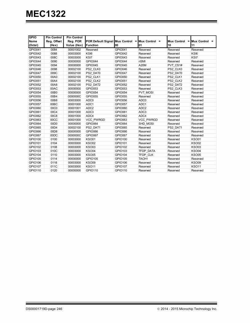
MEC1322
GPIO Name (Octal)
Pin Control Reg. Offset
(Hex)
Pin Control Reg. POR
Value (Hex)POR Default Signal Function
Mux Control = 00
Mux Control = 01
Mux Control = 10
Mux Control = 11
GPIO041 0084 00001002 Reserved GPIO041 Reserved Reserved ReservedGPIO042 0088 00003000 KSI6 GPIO042 Reserved Reserved KSI6GPIO043 008C 00003000 KSI7 GPIO043 Reserved Reserved KSI7GPIO044 0090 00000000 GPIO044 GPIO044 nSMI Reserved ReservedGPIO045 0094 00000000 GPIO045 GPIO045 A20M PVT_CS1# ReservedGPIO046 0098 00002100 PS2_CLK0 GPIO046 Reserved PS2_CLK0 ReservedGPIO047 009C 00002100 PS2_DAT0 GPIO047 Reserved PS2_DAT0 ReservedGPIO050 00A0 00002100 PS2_CLK1 GPIO050 Reserved PS2_CLK1 ReservedGPIO051 00A4 00002100 PS2_CLK2 GPIO051 Reserved PS2_CLK2 ReservedGPIO052 00A8 00002100 PS2_DAT2 GPIO052 Reserved PS2_DAT2 ReservedGPIO053 00AC 00000000 GPIO053 GPIO053 Reserved PS2_CLK3 ReservedGPIO054 00B0 00000000 GPIO054 GPIO054 PVT_MOSI Reserved ReservedGPIO055 00B4 0000000C GPIO055 GPIO055 Reserved Reserved ReservedGPIO056 00B8 00003000 ADC0 GPIO056 ADC0 Reserved ReservedGPIO057 00BC 00001000 ADC1 GPIO057 ADC1 Reserved ReservedGPIO060 00C0 00001001 ADC2 GPIO060 ADC2 Reserved ReservedGPIO061 00C4 00001000 ADC3 GPIO061 ADC3 Reserved ReservedGPIO062 00C8 00001000 ADC4 GPIO062 ADC4 Reserved ReservedGPIO063 00CC 00001000 VCC_PWRGD GPIO063 VCC_PWRGD Reserved ReservedGPIO064 00D0 00000000 GPIO064 GPIO064 SHD_MOSI Reserved ReservedGPIO065 00D4 00002100 PS2_DAT1 GPIO065 Reserved PS2_DAT1 ReservedGPIO066 00D8 00000000 GPIO066 GPIO066 Reserved Reserved ReservedGPIO067 00DC 0000000C GPIO067 GPIO067 Reserved Reserved ReservedGPIO100 0100 00003000 KSO01 GPIO100 Reserved Reserved KSO01GPIO101 0104 00003000 KSO02 GPIO101 Reserved Reserved KSO02GPIO102 0108 00003000 KSO03 GPIO102 Reserved Reserved KSO03GPIO103 010C 00003000 KSO04 GPIO103 TFDP_DATA Reserved KSO04GPIO104 0110 00003000 KSO05 GPIO104 TFDP_CLK Reserved KSO05GPIO105 0114 00000000 GPIO105 GPIO105 TACH1 Reserved ReservedGPIO106 0118 00003000 KSO09 GPIO106 Reserved Reserved KSO09GPIO107 011C 00003000 KSO11 GPIO107 Reserved Reserved KSO11GPIO110 0120 00000000 GPIO110 GPIO110 Reserved Reserved Reserved
DS00001719D-page 246 2014 - 2015 Microchip Technology Inc.

MEC1322
GPIO Name (Octal)
Pin Control Reg. Offset
(Hex)
Pin Control Reg. POR
Value (Hex)POR Default Signal Function
Mux Control = 00
Mux Control = 01
Mux Control = 10
Mux Control = 11
GPIO111 0124 00001000 LAD3 GPIO111 LAD3 Reserved ReservedGPIO112 0128 00001000 LAD0 GPIO112 LAD0 Reserved ReservedGPIO113 012C 00001000 LAD2 GPIO113 LAD2 Reserved ReservedGPIO114 0130 00001000 LAD1 GPIO114 LAD1 Reserved ReservedGPIO115 0134 00001000 SER_IRQ GPIO115 SER_IRQ Reserved ReservedGPIO116 0138 00001000 LRESET# GPIO116 LRESET# Reserved ReservedGPIO117 013C 00001000 PCI_CLK GPIO117 PCI_CLK Reserved ReservedGPIO120 0140 00001000 LFRAME# GPIO120 LFRAME# Reserved ReservedGPIO121 0144 00001000 nRESET_OUT GPIO121 nRESET_OUT Reserved ReservedGPIO122 0148 00000000 GPIO122 GPIO122 SHD_SCLK Reserved ReservedGPIO123 014C 0000000C GPIO123 GPIO123 Reserved Reserved ReservedGPIO124 0150 00000000 GPIO124 GPIO124 SHD_MISO Reserved ReservedGPIO125 0154 00002000 KSI0 GPIO125 Reserved KSI0 ReservedGPIO126 0158 00002000 KSI1 GPIO126 Reserved KSI1 ReservedGPIO127 015C 00000000 GPIO127 GPIO127 PECI_RDY Reserved ReservedGPIO130 0160 00000000 GPIO130 GPIO130 Reserved Reserved ReservedGPIO131 0164 00001100 VCC1_RST# GPIO131 VCC1_RST# Reserved ReservedGPIO132 0168 00000000 GPIO132 GPIO132 PECI_DAT Reserved ReservedGPIO133 016C 00000000 GPIO133 GPIO133 PWM0 Reserved ReservedGPIO134 0170 00002100 I2C0_CLK1 GPIO134 Reserved I2C0_CLK1 ReservedGPIO135 0174 00000000 GPIO135 GPIO135 KBRST Reserved ReservedGPIO136 0178 00000000 GPIO136 GPIO136 PWM1 Reserved ReservedGPIO140 0180 00000000 GPIO140 GPIO140 TACH2 Reserved TACH2PWM_INGPIO141 0184 00000000 GPIO141 GPIO141 PWM3 LED3 ReservedGPIO142 0188 00003000 KSI4 GPIO142 Reserved Reserved KSI4GPIO143 018C 00000200 GPIO143 GPIO143 RSMRST# Reserved ReservedGPIO144 0190 00003000 KSI2 GPIO144 Reserved Reserved KSI2GPIO145 0194 00000001 GPIO145 GPIO145 Reserved Reserved ReservedGPIO146 0198 00000000 GPIO146 GPIO146 PVT_CS0# Reserved ReservedGPIO147 019C 00000001 GPIO147 GPIO147 Reserved Reserved ReservedGPIO150 01A0 00000000 GPIO150 GPIO150 SHD_CS0# Reserved ReservedGPIO151 01A4 00000001 GPIO151 GPIO151 Reserved Reserved Reserved
GPIO Name (Octal)
Pin Control Reg. Offset
(Hex)
Pin Control Reg. POR
Value (Hex)POR Default Signal Function
Mux Control = 00
Mux Control = 01
Mux Control = 10
Mux Control = 11
GPIO152 01A8 00000000 GPIO152 GPIO152 Reserved PS2_DAT3 ReservedGPIO153 01AC 00000000 GPIO153 GPIO153 PVT_SCLK Reserved ReservedGPIO154 01B0 00002000 LED0 GPIO154 Reserved LED0 ReservedGPIO155 01B4 00002000 LED1 GPIO155 Reserved LED1 ReservedGPIO156 01B8 00002000 LED2 GPIO156 Reserved LED2 ReservedGPIO157 01BC 00000001 GPIO157 GPIO157 BC_CLK Reserved ReservedGPIO160 01C0 00000001 GPIO160 GPIO160 BC_DAT Reserved ReservedGPIO161 01C4 00000001 GPIO161 GPIO161 BC_INT# Reserved ReservedGPIO162 01C8 00000000 GPIO162 GPIO162 RXD Reserved ReservedGPIO163 01CC 00000000 GPIO163 GPIO163 Reserved Reserved ReservedGPIO164 01D0 00000000 GPIO164 GPIO164 PVT_MISO Reserved ReservedGPIO165 01D4 00000000 GPIO165 GPIO165 TXD SHD_CS1# ReservedGPIO200 0200 0000000C GPIO200 GPIO200 Reserved Reserved ReservedGPIO201 0204 0000000C GPIO201 GPIO201 Reserved Reserved ReservedGPIO202 0208 0000000C GPIO202 GPIO202 Reserved Reserved ReservedGPIO203 020C 0000000C GPIO203 GPIO203 Reserved Reserved ReservedGPIO204 0210 0000000C GPIO204 GPIO204 Reserved Reserved ReservedGPIO206 0218 00000000 GPIO206 GPIO206 Reserved Reserved ReservedGPIO210 0220 0000000C GPIO210 GPIO210 Reserved Reserved ReservedGPIO211 0224 0000000C GPIO211 GPIO211 Reserved Reserved Reserved
2014 - 2015 Microchip Technology Inc. DS00001719D-page 247

MEC1322
Note 1: The value of the Pin Control Register 2 for each pin is not shown in the tables above. The default value canbe determined by the current value shown in the “Default Operation” column of the Multiplexing Tables inSection 1.5.2, "Multiplexing Tables," on page 20 as follows:
2mA: 00000000h4mA: 00000010h8mA: 00000020h12mA: 00000030h
2: The default slew rate is slow.
3: The GPIO041 pin defaults to output low. This pin must be reprogrammed to the GPIO function upon power-up.
20.7 Pin Multiplexing Control
Pin multiplexing depends upon the Mux Control bits in the Pin Control Register. There is a Pin Control Register foreach GPIO signal function. TABLE 20-5: shows default of the register for each GPIO pin.
The registers listed in the Register Summary table are for a single instance of the MEC1322. The addresses of eachregister listed in this table are defined as a relative offset to the host “Base Address” defined in the Register BaseAddress Table.
Note 20-1 The Base Address indicates where the first register can be accessed in a particular address spacefor a block instance.
Note 20-2 The GPIO registers may be accessed by the LPC Host via the EMI block via GPIO commands or bydirect access if enabled by firmware. See the firmware documentation for a description of this accessmethod.
TABLE 20-6: REGISTER BASE ADDRESS TABLE
Instance NameInstance Number
Host Address Space Base Address (Note 20-1)
GPIO 0 LPC I/O Note 20-2
0 EC 32-bit internal address space
4008_1000h
TABLE 20-7: REGISTER SUMMARY
Offset Register Name
000h - 01Ch GPIO000-GPIO007 Pin Control Register
020h - 03Ch GPIO010-GPIO017 Pin Control Register
040h - 05Ch GPIO020-GPIO027 Pin Control Register
060h - 078h GPIO030-GPIO036 Pin Control Register
080h - 09Ch GPIO040-GPIO047 Pin Control Register
0A0h - 0BCh GPIO050-GPIO057 Pin Control Register
0C0h - 0DCh GPIO060-GPIO067 Pin Control Register
100h - 11Ch GPIO100-GPIO107 Pin Control Register
120h - 13Ch GPIO110-GPIO117 Pin Control Register
140h - 15Ch GPIO120-GPIO127 Pin Control Register
160h - 178h GPIO130-GPIO136 Pin Control Register
180h - 19Ch GPIO140-GPIO147 Pin Control Register
1A0h - 1BCh GPIO150-GPIO157 Pin Control Register
1C0h - 1D4h GPIO160-GPIO165 Pin Control Register
200h - 210h GPIO200-GPIO204 Pin Control Register
218h GPIO206 Pin Control Register
220h - 224h GPIO210-GPIO211 Pin Control Register
280h(Note 20-3)
Output GPIO[000:036]
DS00001719D-page 248 2014 - 2015 Microchip Technology Inc.

MEC1322
Note 20-3 The GPIO input and output registers are LPC I/O accessible via Region 0 of the EMI block. Thisaccess is defined in the EMI Protocols chapter of the firmware specification.
Note 20-4 There is no Pin Control Register 2 for GPIO111-GPIO117 and GPIO120, which are PCI_PIO buffertype pins. The drive strength and slew rate are not configurable on these pins.
284h(Note 20-3)
Output GPIO[040:076]
288h(Note 20-3)
Output GPIO[100:127]
28Ch(Note 20-3)
Output GPIO[140:176]
290h(Note 20-3)
Output GPIO[200:236]
300h(Note 20-3)
Input GPIO[000:036]
304h(Note 20-3)
Input GPIO[040:076]
308h(Note 20-3)
Input GPIO[100:127]
30Ch(Note 20-3)
Input GPIO[140:176]
310h(Note 20-3)
Input GPIO[200:236]
500h - 51Ch GPIO000-GPIO007 Pin Control Register 2
520h - 53Ch GPIO010-GPIO017 Pin Control Register 2
540h - 55Ch GPIO020-GPIO027 Pin Control Register 2
560h - 578h GPIO030-GPIO036 Pin Control Register 2
580h - 59Ch GPIO040-GPIO047 Pin Control Register 2
5A0h - 5BCh GPIO050-GPIO057 Pin Control Register 2
5C0h - 5DCh GPIO060-GPIO067 Pin Control Register 2
5E0h - 5FCh GPIO100-GPIO107 Pin Control Register 2
600h GPIO110 Pin Control Register 2
604h - 623h MCHP Reserved (Note 20-4)
624h - 63Ch GPIO121-GPIO127 Pin Control Register 2
640h - 658h GPIO130-GPIO136 Pin Control Register 2
660h - 67Ch GPIO140-GPIO147 Pin Control Register 2
680h - 69Ch GPIO150-GPIO157 Pin Control Register 2
6A0h - 6B4h GPIO160-GPIO165 Pin Control Register 2
720h - 730h GPIO200-GPIO204 Pin Control Register 2
738h GPIO206 Pin Control Register 2
740h - 744h GPIO210-GPIO211 Pin Control Register 2
TABLE 20-7: REGISTER SUMMARY (CONTINUED)
Offset Register Name
2014 - 2015 Microchip Technology Inc. DS00001719D-page 249

MEC1322
20.8 Pin Control Registers
Two Pin Control Registers are implemented for each GPIO. The Pin Control Register format is described in Section20.8.1, "Pin Control Register," on page 250. The Pin Control Register 2 format is described in Section 20.8.2, "PinControl Register 2," on page 253. Pin Control Register address offsets and defaults are defined in Table 20-5, “PinControl Registers,” on page 245.
20.8.1 PIN CONTROL REGISTER
Note: The following GPIOs that do not exist in the 128-pin package are configured as inputs and grounded in thepackage. Firmware should not attempt to turn those GPIOs into outputs and drive them high, or excessivecurrent will be consumed.
• GPIO067• GPIO055• GPIO210• GPIO200• GPIO202• GPIO201• GPIO203• GPIO204
The following GPIOs that do not exist in the 128-pin package are not connected (NC) in the package. TheseGPIOs should be configured as inputs and the internal pull-down should be enabled.
• GPIO211• GPIO123
Offset See Note 20-5
Bits Description Type DefaultReset Event
31:25 RESERVED RES - -
24 GPIO input from pad
On reads, Bit [24] reflects the state of GPIO input from the pad regardless of setting of Bit [10].
Note: This bit is forced high when the selected power well is offas selected by the Power Gating Signal bits. See bits[3:2].
R Note 20-5 VCC1_RESET
23:17 RESERVED RES - -
16 Alternative GPIO data
If enabled by the Output GPIO Write Enable bit, the Alternative GPIO data bit determines the level on the GPIO pin when the pin is config-ured for the GPIO output function.
On writes:If enabled via the Output GPIO Write Enable0: GPIO[x] out = ‘0’1: GPIO[x] out = ‘1’
Note: If disabled via the Output GPIO Write Enable then theGPIO[x] out pin is unaffected by writing this bit.
On reads:Bit [16] returns the last programmed value, not the value on the pin.
R/W Note 20-5 VCC1_RESET
15:14 RESERVED RES - -
DS00001719D-page 250 2014 - 2015 Microchip Technology Inc.

MEC1322
13:12 Mux Control
The Mux Control field determines the active signal function for a pin.
00 = GPIO Function Selected01 = Signal Function 1 Selected10 = Signal Function 2 Selected11 = Signal Function 3 Selected
R/W Note 20-5 VCC1_RESET
11 Polarity
0 = Non-inverted1 = Inverted
When the Polarity bit is set to ‘1’ and the Mux Control bits are greater than ‘00,’ the selected signal function outputs are inverted and Inter-rupt Detection (int_det) sense defined in Table 20-8, "Edge Enable and Interrupt Detection Bits Definition" is inverted. When the Mux Control field selects the GPIO signal function (Mux = ‘00’), the Polar-ity bit does not effect the output. Regardless of the state of the Mux Control field and the Polarity bit, the state of the pin is always reported without inversion in the GPIO input register.
R/W Note 20-5 VCC1_RESET
10 Output GPIO Write Enable
Every GPIO has two mechanisms to set a GPIO data output: Output GPIO Bit located in the GPIO Output Registers and the Alternative GPIO data bit located in bit 16 of this register.
This control bit determines the source of the GPIO output.0 = Alternative GPIO data write enabledWhen this bit is zero the Alternative GPIO data write is enabled and the Output GPIO is disabled.
1 = Output GPIO enableWhen this bit is one the Alternative GPIO data write is disabled and the Output GPIO is enabled.
Note: See description in Section 20.4, "Accessing GPIOs".
R/W Note 20-5 VCC1_RESET
9 GPIO Direction
0 = Input1 = Output
The GPIO Direction bit controls the buffer direction only when the Mux Control field is ‘00’ selecting the pin signal function to be GPIO. When the Mux Control field is greater than ‘00’ (i.e., a non-GPIO signal function is selected) the GPIO Direction bit has no affect and the selected signal function logic directly controls the pin direc-tion.
R/W Note 20-5 VCC1_RESET
Offset See Note 20-5
Bits Description Type DefaultReset Event
2014 - 2015 Microchip Technology Inc. DS00001719D-page 251
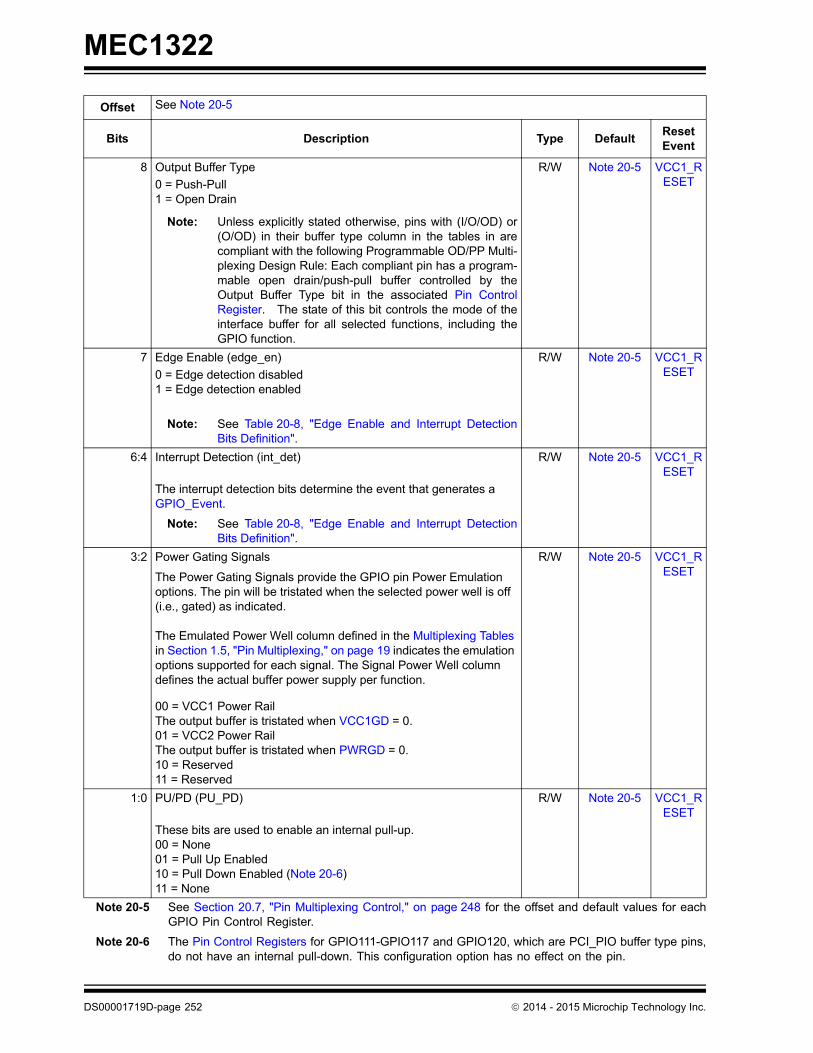
MEC1322
Note 20-5 See Section 20.7, "Pin Multiplexing Control," on page 248 for the offset and default values for eachGPIO Pin Control Register.
Note 20-6 The Pin Control Registers for GPIO111-GPIO117 and GPIO120, which are PCI_PIO buffer type pins,do not have an internal pull-down. This configuration option has no effect on the pin.
8 Output Buffer Type
0 = Push-Pull1 = Open Drain
Note: Unless explicitly stated otherwise, pins with (I/O/OD) or(O/OD) in their buffer type column in the tables in arecompliant with the following Programmable OD/PP Multi-plexing Design Rule: Each compliant pin has a program-mable open drain/push-pull buffer controlled by theOutput Buffer Type bit in the associated Pin ControlRegister. The state of this bit controls the mode of theinterface buffer for all selected functions, including theGPIO function.
R/W Note 20-5 VCC1_RESET
7 Edge Enable (edge_en)
0 = Edge detection disabled1 = Edge detection enabled
Note: See Table 20-8, "Edge Enable and Interrupt DetectionBits Definition".
R/W Note 20-5 VCC1_RESET
6:4 Interrupt Detection (int_det)
The interrupt detection bits determine the event that generates a GPIO_Event.
Note: See Table 20-8, "Edge Enable and Interrupt DetectionBits Definition".
R/W Note 20-5 VCC1_RESET
3:2 Power Gating Signals
The Power Gating Signals provide the GPIO pin Power Emulation options. The pin will be tristated when the selected power well is off (i.e., gated) as indicated.
The Emulated Power Well column defined in the Multiplexing Tables in Section 1.5, "Pin Multiplexing," on page 19 indicates the emulation options supported for each signal. The Signal Power Well column defines the actual buffer power supply per function.
00 = VCC1 Power RailThe output buffer is tristated when VCC1GD = 0.01 = VCC2 Power Rail The output buffer is tristated when PWRGD = 0.10 = Reserved11 = Reserved
R/W Note 20-5 VCC1_RESET
1:0 PU/PD (PU_PD)
These bits are used to enable an internal pull-up.00 = None01 = Pull Up Enabled10 = Pull Down Enabled (Note 20-6)11 = None
R/W Note 20-5 VCC1_RESET
Offset See Note 20-5
Bits Description Type DefaultReset Event
DS00001719D-page 252 2014 - 2015 Microchip Technology Inc.

MEC1322
APPLICATION NOTE: All GPIO interrupt detection configurations default to '0000', which is low level interrupt.Having interrupt detection enabled will un-gated the clock to the GPIO module whenever theinterrupt is active, which increases power consumption. Interrupt detection should bedisabled when not required to save power; this is especially true for pin interfaces (i.e., LPC).
20.8.2 PIN CONTROL REGISTER 2
20.8.3 GPIO OUTPUT REGISTERS
If enabled by the Output GPIO Write Enable bit, the GPIO Output bits determine the level on the GPIO pin when the pinis configured for the GPIO output function.
On writes:
If enabled via the Output GPIO Write Enable
0: GPIO[x] out = ‘0’
1: GPIO[x] out = ‘1’
If disabled via the Output GPIO Write Enable then the GPIO[x] out pin is unaffected by writing this bit.
TABLE 20-8: EDGE ENABLE AND INTERRUPT DETECTION BITS DEFINITION
Edge Enable
Interrupt Detection BitsSelected Function
D7 D6 D5 D4
0 0 0 0 Low Level Sensitive
0 0 0 1 High Level Sensitive
0 0 1 0 Reserved
0 0 1 1 Reserved
0 1 0 0 Interrupt events are disabled
0 1 0 1 Reserved
0 1 1 0 Reserved
0 1 1 1 Reserved
1 1 0 1 Rising Edge Triggered
1 1 1 0 Falling Edge Triggered
1 1 1 1 Either edge triggered
Note: Only edge triggered interrupts can wake up the main ring oscillator. The GPIO must be enabled for edge-triggered interrupts and the GPIO interrupt must be enabled in the interrupt aggregator in order to wake upthe ring when the ring is shut down.
Offset See Note 20-5
Bits Description Type DefaultReset Event
31:6 RESERVED RES - -
5:4 Drive Strength These bits are used to select the drive strength on the pin.00 = 2mA01 = 4mA10 = 8mA11 = 12mA
R/W Note 1: on page 248
VCC1_RESET
3:1 RESERVED RES - -
0 Slew Rate This bit is used to select the slew rate on the pin.0 = slow (half frequency)1 = fast
R/W 0 VCC1_RESET
2014 - 2015 Microchip Technology Inc. DS00001719D-page 253

MEC1322
On reads:
Bit [16] returns the last programmed value, not the value on the pin.
20.8.3.1 Output GPIO[000:036]
20.8.3.2 Output GPIO[040:076]
20.8.3.3 Output GPIO[100:127]
Note: Bits associated with GPIOs that are not implemented are shown as Reserved.
Offset 280h (Note 20-3)
Bits Description Type DefaultReset Event
31 RESERVED RES - -
30:24 GPIO[036:030] Output R/W 00h VCC1_RESET
23:16 GPIO[027:020] Output R/W 00h VCC1_RESET
15:8 GPIO[017:010] Output R/W 00h VCC1_RESET
7:0 GPIO[007:000] Output R/W 00h VCC1_RESET
Offset 284h (Note 20-3)
Bits Description Type DefaultReset Event
31:24 RESERVED RES - -
23:16 GPIO[067:060] Output R/W 00h VCC1_RESET
15:8 GPIO[057:050] Output R/W 00h VCC1_RESET
7:0 GPIO[047:040] Output R/W 00h VCC1_RESET
Offset 288h (Note 20-3)
Bits Description Type DefaultReset Event
31 RESERVED RES - -
30:24 GPIO[136:130] Output R/W 00h VCC1_RESET
23:16 GPIO[127:120] Output R/W 00h VCC1_RESET
15:8 GPIO[117:110] Output R/W 00h VCC1_RESET
7:0 GPIO[107:100] Output R/W 00h VCC1_RESET
DS00001719D-page 254 2014 - 2015 Microchip Technology Inc.

MEC1322
20.8.3.4 Output GPIO[140:176]
20.8.3.5 Output GPIO[200:236]
20.8.4 GPIO INPUT REGISTERS
The GPIO Input Registers can always be used to read the state of a pin, even when the pin is in an output mode and/orwhen a signal function other than the GPIO signal function is selected; i.e., the Pin Control Register Mux Control bitsare not equal to ‘00.’
The MSbit of the Input GPIO registers have been implemented as a read/write scratch pad bit to support processor spe-cific instructions.
Offset 28Ch (Note 20-3)
Bits Description Type DefaultReset Event
31:22 RESERVED RES - -
21:16 GPIO[165:160] Output R/W 00h VCC1_RESET
15:8 GPIO[157:150] Output R/W 00h VCC1_RESET
7:0 GPIO[147:140] Output R/W 00h VCC1_RESET
Offset 290h (Note 20-3)
Bits Description Type DefaultReset Event
31 RESERVED RES - -
30:24 RESERVED RES - -
23:12 RESERVED RES - -
11:10 MCHP Reserved R/W 00h VCC1_RESET
9:8 GPIO[211:210] Output R/W 00h VCC1_RESET
7 RESERVED RES - -
6 GPIO206 Output R/W 00h VCC1_RESET
5 RESERVED RES - -
4:0 GPIO[204:200] Output R/W 00h VCC1_RESET
Note: Bits associated with GPIOs that are not implemented are shown as Reserved.
2014 - 2015 Microchip Technology Inc. DS00001719D-page 255

MEC1322
20.8.4.1 Input GPIO[000:036]
20.8.4.2 Input GPIO[040:076]
20.8.4.3 Input GPIO[100:127]
Offset 300h (Note 20-3)
Bits Description Type DefaultReset Event
31 Scratchpad Bit R/W 0b VCC1_RESET
30:24 GPIO[036:030] Input R 00h VCC1_RESET
23:16 GPIO[027:020] Input R 00h VCC1_RESET
15:8 GPIO[017:010] Input R 00h VCC1_RESET
7:0 GPIO[007:000] Input R 00h VCC1_RESET
Offset 304h (Note 20-3)
Bits Description Type DefaultReset Event
31 Scratchpad Bit R/W 0b VCC1_RESET
30:24 RESERVED R - -
23:16 GPIO[067:060] Input R 00h VCC1_RESET
15:8 GPIO[057:050] Input R 00h VCC1_RESET
7:0 GPIO[047:040] Input R 00h VCC1_RESET
Offset 308h (Note 20-3)
Bits Description Type DefaultReset Event
31 Scratchpad Bit R/W 0b VCC1_RESET
30:24 GPIO[136:130] Input R 00h VCC1_RESET
23:16 GPIO[127:120] Input R 00h VCC1_RESET
15:8 GPIO[117:110] Input R 00h VCC1_RESET
7:0 GPIO[107:100] Input R 00h VCC1_RESET
DS00001719D-page 256 2014 - 2015 Microchip Technology Inc.

MEC1322
20.8.4.4 Input GPIO[140:176]
20.8.4.5 Input GPIO[200:236]
Offset 30Ch(Note 20-3)
Bits Description Type DefaultReset Event
31 Scratchpad Bit R/W 0b VCC1_RESET
30:22 Reserved R 00h VCC1_RESET
21:16 GPIO[165:160] Input R 00h VCC1_RESET
15:8 GPIO[157:150] Input R 00h VCC1_RESET
7:0 GPIO[147:140] Input R 00h VCC1_RESET
Offset 310h(Note 20-3)
Bits Description Type DefaultReset Event
31 Scratchpad Bit R/W 0b VCC1_RESET
30:24 Scratchpad Bits R/W 00h VCC1_RESET
23:16 Scratchpad Bits R/W 00h VCC1_RESET
15:12 RESERVED RES - -
11:10 MCHP Reserved R/W 00h VCC1_RESET
9:8 GPIO[211:210] Input R/W 00h VCC1_RESET
7 RESERVED RES - -
6 GPIO206 Input R/W 00h VCC1_RESET
5 RESERVED RES - -
4:0 GPIO[204:200] Input R/W 00h VCC1_RESET
2014 - 2015 Microchip Technology Inc. DS00001719D-page 257

MEC1322
21.0 INTERNAL DMA CONTROLLER
21.1 Introduction
The Internal DMA Controller transfers data to/from the source from/to the destination. The firmware is responsible forsetting up each channel. Afterwards either the firmware or the hardware may perform the flow control. The hardwareflow control exists entirely inside the source device. Each transfer may be 1, 2, or 4 bytes in size, so long as the devicesupports a transfer of that size. Every device must be on the internal 32-bit address space.
21.2 References
No references have been cited for this chapter
21.3 Terminology
TABLE 21-1: TERMINOLOGY
Term Definition
DMA Transfer This is a complete DMA Transfer which is done after the Master Device terminates the transfer, the Firmware Aborts the transfer or the DMA reaches its transfer limit.A DMA Transfer may consist of one or more data packets.
Data Packet Each data packet may be composed of 1, 2, or 4 bytes. The size of the data packet is limited by the max size supported by both the source and the des-tination. Both source and destination will transfer the same number of bytes per packet.
Channel The Channel is responsible for end-to-end (source-to-destination) Data Packet delivery.
Device A Device may refer to a Master or Slave connected to the DMA Channel. Each DMA Channel may be assigned one or more devices.
Master Device This is the master of the DMA, which determines when it is active.The Firmware is the master while operating in Firmware Flow Control.The Hardware is the master while operating in Hardware Flow Control.
The Master Device in Hardware Mode is selected by DMA Channel Con-trol:Hardware Flow Control Device. It is the index of the Flow Control Port.
Slave Device The Slave Device is defined as the device associated with the targeted Memory Address.
Source The DMA Controller moves data from the Source to the Destination. The Source provides the data. The Source may be either the Master or Slave Controller.
Destination The DMA Controller moves data from the Source to the Destination. The Destination receives the data. The Destination may be either the Master or Slave Controller.
DS00001719D-page 258 2014 - 2015 Microchip Technology Inc.

MEC1322
21.4 Interface
This block is designed to be accessed externally via the pin interface and internally via a registered host interface.
21.4.1 SIGNAL DESCRIPTION
This block doesn’t have any external signals that may be routed to the pin interface. This DMA Controller is intended tobe used internally to transfer large amounts of data without the embedded controller being actively involved in the trans-fer.
21.4.2 HOST INTERFACE
The registers defined for the Internal DMA Controller are accessible by the various hosts as indicated in Section 21.9,"EC-Only Registers".
21.4.3 DMA INTERFACE
Each DMA Master Device that may engage in a DMA transfer must have a compliant DMA interface. The following tablelists the DMA Devices in the MEC1322.
Note 21-1 The Device Number is programmed into field HARDWARE_FLOW_CONTROL_DEVICE of the DMAChannel N Control register.
FIGURE 21-1: INTERNAL DMA CONTROLLER I/O DIAGRAM
TABLE 21-2: DMA CONTROLLER DEVICE SELECTION
Device NameDevice Number
(Note 21-1)Controller Source
SMBus 0 Controller 0 Slave
1 Master
SMBus 1 Controller 2 Slave
3 Master
SMBus 2 Controller 4 Slave
5 Master
SMBus 3 Controller 6 Slave
7 Master
SPI 0 Controller 8 Transmit
9 Receive
SPI 1 Controller 10 Transmit
11 Receive
Internal DMA Controller
Power, Clocks and Reset
Interrupts
DMA Interface
Host Interface
2014 - 2015 Microchip Technology Inc. DS00001719D-page 259

MEC1322
TABLE 21-3: DMA CONTROLLER MASTER DEVICES SIGNAL LIST
Device NameDev Num(21.5)
Device Signal Name Direction Description
SMBus 0 Controller 0 SMB_SDMA_Req INPUT DMA request control from SMBus Slave channel.
SMB_SDMA_Term INPUT DMA termination control from SMBus Slave channel.
SMB_SDMA_Done OUTPUT DMA termination control from DMA Con-troller to Slave channel.
1 SMB_MDMA_Req INPUT DMA request control from SMBus Master channel.
SMB_MDMA_Term INPUT DMA termination control from SMBus Mas-ter channel.
SMB_MDMA_Done OUTPUT DMA termination control from DMA Con-troller to Master channel.
SMBus 1 Controller 2 SMB_SDMA_Req INPUT DMA request control from SMBus Slave channel.
SMB_SDMA_Term INPUT DMA termination control from SMBus Slave channel.
SMB_SDMA_Done OUTPUT DMA termination control from DMA Con-troller to Slave channel.
3 SMB_MDMA_Req INPUT DMA request control from SMBus Master channel.
SMB_MDMA_Term INPUT DMA termination control from SMBus Mas-ter channel.
SMB_MDMA_Done OUTPUT DMA termination control from DMA Con-troller to Master channel.
SMBus 2 Controller 4 SMB_SDMA_Req INPUT DMA request control from SMBus Slave channel.
SMB_SDMA_Term INPUT DMA termination control from SMBus Slave channel.
SMB_SDMA_Done OUTPUT DMA termination control from DMA Con-troller to Slave channel.
5 SMB_MDMA_Req INPUT DMA request control from SMBus Master channel.
SMB_MDMA_Term INPUT DMA termination control from SMBus Mas-ter channel.
SMB_MDMA_Done OUTPUT DMA termination control from DMA Con-troller to Master channel.
DS00001719D-page 260 2014 - 2015 Microchip Technology Inc.

MEC1322
21.5 Power, Clocks and Reset
This section defines the Power, Clock, and Reset parameters of the block.
21.5.1 POWER DOMAINS
21.5.2 CLOCK INPUTS
SMBus 3 Controller 6 SMB_SDMA_Req INPUT DMA request control from SMBus Slave channel.
SMB_SDMA_Term INPUT DMA termination control from SMBus Slave channel.
SMB_SDMA_Done OUTPUT DMA termination control from DMA Con-troller to Slave channel.
7 SMB_MDMA_Req INPUT DMA request control from SMBus Master channel.
SMB_MDMA_Term INPUT DMA termination control from SMBus Mas-ter channel.
SMB_MDMA_Done OUTPUT DMA termination control from DMA Con-troller to Master channel.
SPI 0 Controller 8 SPI_SDMA_Req INPUT DMA request control from SPI TX channel.
SPI_SDMA_Term INPUT DMA termination control from SPI TX channel. Not supported.
SPI_SDMA_Done OUTPUT DMA termination control from DMA Con-troller to TX Channel. Not supported.
9 SPI_MDMA_Req INPUT DMA request control from SPI RX channel.
SPI_MDMA_Term INPUT DMA termination control from SPI RX channel. Not supported.
SPI_MDMA_Done OUTPUT DMA termination control from DMA Con-troller to RX channel. Not supported.
SPI 1 Controller 10 SPI_SDMA_Req INPUT DMA request control from SPI TX channel.
SPI_SDMA_Term INPUT DMA termination control from SPI TX channel. Not supported.
SPI_SDMA_Done OUTPUT DMA termination control from DMA Con-troller to TX Channel. Not supported.
11 SPI_MDMA_Req INPUT DMA request control from SPI RX channel.
SPI_MDMA_Term INPUT DMA termination control from SPI RX channel. Not supported.
SPI_MDMA_Done OUTPUT DMA termination control from DMA Con-troller to RX channel. Not supported.
TABLE 21-4: POWER SOURCES
Name Description
VCC1 This power well sources the registers and logic in this block.
TABLE 21-5: CLOCK INPUTS
Name Description
48 MHz Ring Oscillator This clock signal drives selected logic (e.g., counters).
TABLE 21-3: DMA CONTROLLER MASTER DEVICES SIGNAL LIST (CONTINUED)
Device NameDev Num(21.5)
Device Signal Name Direction Description
2014 - 2015 Microchip Technology Inc. DS00001719D-page 261

MEC1322
21.5.3 RESETS
21.6 Interrupts
This section defines the Interrupt Sources generated from this block.
21.7 Low Power Modes
The Internal DMA Controller may be put into a low power state by the chip’s Power, Clocks, and Reset (PCR) circuitry.
When the block is commanded to go to sleep it will place the DMA block into sleep mode only after all transactions onthe DMA have been completed. For Firmware Flow Controlled transactions, the DMA will wait until it hits its terminalcount and clears the Go control bit. For Hardware Flow Control, the DMA will go to sleep after either the terminal countis hit, or the Master device flags the terminate signal.
21.8 Description
The MEC1322 features a 12 channel DMA controller. The DMA controller can autonomously move data from/to anyDMA capable master device to/from any populated memory location. This mechanism allows hardware IP blocks totransfer large amounts of data into or out of memory without EC intervention.
The DMA has the following characteristics:
• Data is only moved 1 Data Packet at a time
• Data only moves between devices on the accessible via the internal 32-bit address space
TABLE 21-6: RESET SIGNALS
Name Description
VCC1_RESET This reset signal resets all of the registers and logic in this block.
RESET This reset is generated if either the VCC1_RESET is asserted or the SOFT_RESET is asserted.
TABLE 21-7: INTERRUPTS
Source Description
DMA0 Direct Memory Access Channel 0This signal is generated by the STATUS_DONE bit.
DMA1 Direct Memory Access Channel 1This signal is generated by the STATUS_DONE bit.
DMA2 Direct Memory Access Channel 2This signal is generated by the STATUS_DONE bit.
DMA3 Direct Memory Access Channel 3This signal is generated by the STATUS_DONE bit.
DMA4 Direct Memory Access Channel 4This signal is generated by the STATUS_DONE bit.
DMA5 Direct Memory Access Channel 5This signal is generated by the STATUS_DONE bit.
DMA6 Direct Memory Access Channel 6This signal is generated by the STATUS_DONE bit.
DMA7 Direct Memory Access Channel 7This signal is generated by the STATUS_DONE bit.
DMA8 Direct Memory Access Channel 8This signal is generated by the STATUS_DONE bit.
DMA9 Direct Memory Access Channel 9This signal is generated by the STATUS_DONE bit.
DMA10 Direct Memory Access Channel 10This signal is generated by the STATUS_DONE bit.
DMA11 Direct Memory Access Channel 11This signal is generated by the STATUS_DONE bit.
DS00001719D-page 262 2014 - 2015 Microchip Technology Inc.

MEC1322
• The DMA Controller has 12 DMA Channels
• Each DMA Channel may be configured to communicate with any DMA capable device on the 32-bit internal address space. Each device has been assigned a device number. See Section 21.4.3, "DMA Interface," on page 259.
The controller will accesses SRAM buffers only with incrementing addresses (that is, it cannot start at the top of a buffer,nor does it handle circular buffers automatically). The controller does not handle chaining (that is, automatically startinga new DMA transfer when one finishes).
21.8.1 CONFIGURATION
The DMA Controller is enabled via the ACTIVATE bit in DMA Main Control register.
Each DMA Channel must also be individually enabled via the CHANNEL_ACTIVATE bit in the DMA Channel N Activateto be operational.
Before starting a DMA transaction on a DMA Channel the host must assign a DMA Master to the channel via HARD-WARE_FLOW_CONTROL_DEVICE. The host must not configure two different channels to the same DMA Master atthe same time.
Data will be transfered between the DMA Master, starting at the programmed DEVICE_ADDRESS, and the targetedmemory location, starting at the MEMORY_START_ADDRESS. The address for either the DMA Master or the targetedmemory location may remain static or it may increment. To enable the DMA Master to increment its address set theINCREMENT_DEVICE_ADDRESS bit. To enable the targeted memory location to increment its addresses set theINCREMENT_MEMORY_ADDRESS. The DMA transfer will continue as long as the target memory address beingaccessed is less than the MEMORY_END_ADDRESS. If the DMA Controller detects that the memory location it isattempting to access on the Target is equal to the MEMORY_END_ADDRESS it will notify the DMA Master that thetransaction is done. Otherwise the Data will be transferred in packets. The size of the packet is determined by theTRANSFER_SIZE.
21.8.2 OPERATION
The DMA Controller is designed to move data from one memory location to another.
21.8.2.1 Establishing a Connection
A DMA Master will initiate a DMA Transaction by requesting access to a channel. The DMA arbiter, which evaluateseach channel request using a basic round robin algorithm, will grant access to the DMA master. Once granted, the chan-nel will hold the grant until it decides to release it, by notifying the DMA Controller that it is done.
21.8.2.2 Initiating a Transfer
Once a connection is established the DMA Master will issue a DMA request to start a DMA transfer. If Firmware wantsto have a transfer request serviced it must set the RUN bit to have its transfer requests serviced.
Firmware can initiate a transaction by setting the TRANSFER_GO bit. The DMA transfer will remain active until eitherthe Master issues a Terminate or the DMA Controller signals that the transfer is DONE. Firmware may terminate a trans-action by setting the TRANSFER_ABORT bit.
Data may be moved from the DMA Master to the targeted Memory address or from the targeted Memory Address to theDMA Master. The direction of the transfer is determined by the TRANSFER_DIRECTION bit.
Once a transaction has been initiated firmware can use the STATUS_DONE bit to determine when the transaction iscompleted. This status bit is routed to the interrupt interface. In the same register there are additional status bits thatindicate if the transaction completed successfully or with errors. This bits are OR’d together with the STATUS_DONEbit to generate the interrupt event. Each status be may be individually enabled/disabled from generating this event.
Note: If Firmware wants to prevent any other channels from being granted while it is active it can set theLOCK_CHANNEL bit.
Note: Before initiating a DMA transaction via firmware the hardware flow control mus be disabled via the DIS-ABLE_HARDWARE_FLOW_CONTROL bit.
2014 - 2015 Microchip Technology Inc. DS00001719D-page 263

MEC1322
21.9 EC-Only Registers
The DMA Controller consists of a Main Block and a number of Channels. Table 21-9, "Main EC-Only Register Summary"lists the registers in the Main Block and Table 21-10, "Channel EC-Only Register Summary" lists the registers in eachchannel. The addresses of each register listed in these tables are defined as a relative offset to the “Base Address”defined in the EC-Only Register Base Address Table. The Base Address for the Main Block and each Channel is definedin the table:
The Base Address indicates where the first register can be accessed in a particular address space for a block instance.
TABLE 21-8: EC-ONLY REGISTER BASE ADDRESS TABLE
Instance NameChannel Number
Host Address Space Base Address
DMA Controller Main Block EC 32-bit internal address space
4000_2400h
DMA Controller 0 EC 32-bit internal address space
4000_2410h
DMA Controller 1 EC 32-bit internal address space
4000_2430h
DMA Controller 2 EC 32-bit internal address space
4000_2450h
DMA Controller 3 EC 32-bit internal address space
4000_2470h
DMA Controller 4 EC 32-bit internal address space
4000_2490h
DMA Controller 5 EC 32-bit internal address space
4000_24B0h
DMA Controller 6 EC 32-bit internal address space
4000_24D0h
DMA Controller 7 EC 32-bit internal address space
4000_24F0h
DMA Controller 8 EC 32-bit internal address space
4000_2510h
DMA Controller 9 EC 32-bit internal address space
4000_2530h
DMA Controller 10 EC 32-bit internal address space
4000_2550h
DMA Controller 11 EC 32-bit internal address space
4000_2570h
TABLE 21-9: MAIN EC-ONLY REGISTER SUMMARY
Offset REGISTER NAME (Mnemonic)
00h DMA Main Control
04h DMA Data Packet
DS00001719D-page 264 2014 - 2015 Microchip Technology Inc.

MEC1322
21.9.1 DMA MAIN CONTROL
21.9.2 DMA DATA PACKET
Note 21-2 The letter ‘N’ following DMA Channel indicates the Channel Number. Each Channel implemented willhave these registers to determine that channel’s operation.
21.9.3 DMA CHANNEL N ACTIVATE
Offset 00h
Bits Description Type DefaultReset Event
7:2 Reserved R - -
1 SOFT_RESET
Soft reset the entire module.
This bit is self-clearing.
W 0b -
0 ACTIVATE
Enable the blocks operation.
1=Enable block. Each individual channel must be enabled separately.0=Disable all channels.
R/WS 0b RESET
Offset 04h
Bits Description Type DefaultReset Event
31:0 DATA_PACKET
Debug register that has the data that is stored in the Data Packet. This data is read data from the currently active transfer source.
R 0000h -
TABLE 21-10: CHANNEL EC-ONLY REGISTER SUMMARY
OffsetRegister Name (Mnemonic)
(Note 21-2)
00h DMA Channel N Activate
04h DMA Channel N Memory Start Address
08h DMA Channel N Memory End Address
0Ch DMA Channel N Device Address
10h DMA Channel N Control
14h DMA Channel N Interrupt Status
18h DMA Channel N Interrupt Enable
Offset 00h
Bits Description Type DefaultReset Event
7:1 Reserved R - -
0 CHANNEL_ACTIVATE
Enable this channel for operation.The DMA Main Control:Activate must also be enabled for this chan-nel to be operational.
R/W 0h RESET
2014 - 2015 Microchip Technology Inc. DS00001719D-page 265

MEC1322
21.9.4 DMA CHANNEL N MEMORY START ADDRESS
21.9.5 DMA CHANNEL N MEMORY END ADDRESS
Offset 04h
Bits Description Type DefaultReset Event
31:0 MEMORY_START_ADDRESS
This is the starting address for the Memory device.
This field is updated by Hardware after every packet transfer by the size of the transfer, as defined by DMA Channel Control:Channel Transfer Size while the DMA Channel Control:Increment Memory Address is Enabled.
The Memory device is defined as the device that is the slave device in the transfer.
ex. With Hardware Flow Control, the Memory device is the device that is not connected to the Hardware Flow Controlling device.
Note: This field is only as large as the maximum allowed AHBAddress Size in the system. If the HADDR size is 24 Bits,then Bits [31:24] will be RESERVED.
R/W 0000h RESET
Offset 08h
Bits Description Type DefaultReset Event
31:0 MEMORY_END_ADDRESS
This is the ending address for the Memory device.
This will define the limit of the transfer, so long as DMA Channel Control:Increment Memory Address is Enabled. When the Memory Start Address is equal to this value, the DMA will terminate the trans-fer and flag the status DMA Channel Interrupt:Status Done.
Note: This field is only as large as the maximum allowed AHBAddress Size in the system. If the HADDR size is 24 Bits,then Bits [31:24] will be RESERVED.
R/W 0000h RESET
DS00001719D-page 266 2014 - 2015 Microchip Technology Inc.

MEC1322
21.9.6 DMA CHANNEL N DEVICE ADDRESS
21.9.7 DMA CHANNEL N CONTROL
Offset 0Ch
Bits Description Type DefaultReset Event
31:0 DEVICE_ADDRESS
This is the Master Device address.
This is used as the address that will access the Device on the DMA. The Device is defined as the Master of the DMA transfer; as in the device that is controlling the Hardware Flow Control.
This field is updated by Hardware after every Data Packet transfer by the size of the transfer, as defined by DMA Channel Con-trol:Transfer Size while the DMA Channel Control:Increment Device Address is Enabled.
Note: This field is only as large as the maximum allowed AHBAddress Size in the system. If the HADDR size is 24 Bits,then Bits [31:24] will be RESERVED.
R/W 0000h RESET
Offset 10h
Bits Description Type DefaultReset Event
31:26 Reserved R - -
25 TRANSFER_ABORT
This is used to abort the current transfer on this DMA Channel. The aborted transfer will be forced to terminate immediately.
R/W 0h RESET
24 TRANSFER_GO
This is used for the Firmware Flow Control DMA transfer.
This is used to start a transfer under the Firmware Flow Control. Do not use this in conjunction with the Hardware Flow Control; DMA Channel Control:Disable Hardware Flow Control must be set in order for this field to function correctly.
R/W 0h RESET
23 Reserved R - -
22:20 TRANSFER_SIZE
This is the transfer size in Bytes of each Data Packet transfer.
Note: The transfer size must be a legal transfer size. Validsizes are 1, 2 and 4 Bytes.
R/W 0h RESET
19 DISABLE_HARDWARE_FLOW_CONTROL
This will Disable the Hardware Flow Control. When disabled, any DMA Master device attempting to communicate to the DMA over the DMA Flow Control Interface (Ports: dma_req, dma_term, and dma_done) will be ignored.This should be set before using the DMA channel in Firmware Flow Control mode.
RW 0h RESET
2014 - 2015 Microchip Technology Inc. DS00001719D-page 267

MEC1322
18 LOCK_CHANNEL
This is used to lock the arbitration of the Channel Arbiter on this channel once this channel is granted.Once this is locked, it will remain on the arbiter until it has completed it transfer (either the Transfer Aborted, Transfer Done or Transfer Terminated conditions).
Note: This setting may starve other channels if the locked chan-nel takes an excessive period of time to complete.
RW 0h RESET
17 INCREMENT_DEVICE_ADDRESS
This will enable an auto-increment to the DMA Channel Device Address.
1: Increment the DMA Channel Device Address by DMA ChannelControl:Transfer Size after every Data Packet transfer
0: Do nothing
RW 0h RESET
16 INCREMENT_MEMORY_ADDRESS
This will enable an auto-increment to the DMA Channel Memory Address.
1=Increment the DMA Channel Memory Address by DMA ChannelControl:Transfer Size after every Data Packet transfer
0=Do nothing
Note: If this is not set, the DMA will never terminate the transferon its own. It will have to be terminated through the Hard-ware Flow Control or through a DMA Channel Con-trol:Transfer Abort.
RW 0h RESET
15:9 HARDWARE_FLOW_CONTROL_DEVICE
This is the device that is connected to this channel as its Hardware Flow Control master.The Flow Control Interface is a bus with each master concatenated onto it. This selects which bus index of the concatenated Flow Con-trol Interface bus is targeted towards this channel.The Flow Control Interface Port list is dma_req, dma_term, and dma_done.
RW 0h RESET
8 TRANSFER_DIRECTION
This determines the direction of the DMA Transfer.
1=Data Packet Read from Memory Start Address followed by DataPacket Write to Device Address
0=Data Packet Read from Device Address followed by Data PacketWrite to Memory Start Address
RW 0h RESET
7:6 Reserved R - -
5 BUSY
This is a status signal.
1=The DMA Channel is busy (FSM is not IDLE)0=The DMA Channel is not busy (FSM is IDLE)
RO 0h RESET
Offset 10h
Bits Description Type DefaultReset Event
DS00001719D-page 268 2014 - 2015 Microchip Technology Inc.

MEC1322
4:3 STATUS
This is a status signal. The status decode is listed in priority order with the highest priority first.
3: Error detected by the DMA2: The DMA Channel is externally done, in that the Device has termi-
nated the transfer over the Hardware Flow Control through thePort dma_term
1: The DMA Channel is locally done, in that Memory Start Addressequals Memory End Address
0: DMA Channel Control:Run is Disabled (0x0)
Note: This functionality has been replaced by the Interrupt field,and as such should never be used.
The field will not flag back appropriately timed status, andif used may cause the firmware to become out-of-syncwith the hardware.
This field has multiple non-exclusive statuses, but mayonly display a single status. As such, multiple statusesmay be TRUE, but this will appear as though only a singlestatus has been triggered.
R 0h RESET
2 DONE
This is a status signal. It is only valid while DMA Channel Con-trol:Run is Enabled. This is the inverse of the DMA Channel Con-trol:Busy field, except this is qualified with the DMA Channel Control:Run field.
1=Channel is done0=Channel is not done or it is OFF
RO 0h RESET
1 REQUEST
This is a status field.
1= There is a transfer request from the Master Device0= There is no transfer request from the Master Device
RO 0h RESET
0 RUN
This is a control field.
Note: This bit only applies to Hardware Flow Control mode.
1= This channel is enabled and will service transfer requests0=This channel is disabled. All transfer requests are ignored
RW 0h RESET
Offset 10h
Bits Description Type DefaultReset Event
2014 - 2015 Microchip Technology Inc. DS00001719D-page 269

MEC1322
21.9.8 DMA CHANNEL N INTERRUPT STATUS
21.9.9 DMA CHANNEL N INTERRUPT ENABLE
Offset 14h
Bits Description Type DefaultReset Event
7:3 Reserved R - -
2 STATUS_DONE
This is an interrupt source register.This flags when the DMA Channel has completed a transfer suc-cessfully on its side.A completed transfer is defined as when the DMA Channel reaches its limit; Memory Start Address equals Memory End Address.A completion due to a Hardware Flow Control Terminate will not flag this interrupt.
1=Memory Start Address equals Memory End Address0=Memory Start Address does not equal Memory End Address
R/WC 0h RESET
1 STATUS_FLOW_CONTROL
This is an interrupt source register.This flags when the DMA Channel has encountered a Hardware Flow Control Request after the DMA Channel has completed the transfer. This means the Master Device is attempting to overflow the DMA.
1=Hardware Flow Control is requesting after the transfer has com-pleted
0=No Hardware Flow Control event
0h RESET
0 STATUS_BUS_ERROR
This is an interrupt source register.This flags when there is an Error detected over the internal 32-bit Bus.
1: Error detected.
R/WC 0h RESET
Offset 18h
Bits Description Type DefaultReset Event
7:3 Reserved R - -
2 STATUS_ENABLE_DONE
This is an interrupt enable for DMA Channel Interrupt:Status Done.
1=Enable Interrupt0=Disable Interrupt
R/W 0h RESET
1 STATUS_ENABLE_FLOW_CONTROL_ERROR
This is an interrupt enable for DMA Channel Interrupt:Status Flow Control Error.
1=Enable Interrupt0=Disable Interrupt
R/W 0h RESET
DS00001719D-page 270 2014 - 2015 Microchip Technology Inc.

MEC1322
0 STATUS_ENABLE_BUS_ERROR
This is an interrupt enable for DMA Channel Interrupt:Status Bus Error.
1=Enable Interrupt0=Disable Interrupt
R/W 0h RESET
Offset 18h
Bits Description Type DefaultReset Event
2014 - 2015 Microchip Technology Inc. DS00001719D-page 271

MEC1322
22.0 SMBUS INTERFACE
22.1 Introduction
The MEC1322 SMBus Interface includes one instance of the SMBus controller core. This chapter describes aspects ofthe SMBus Interface that are unique to the MEC1322 instantiations of this core; including, Power Domain, Resets,Clocks, Interrupts, Registers and the Physical Interface. For a General Description, Features, Block Diagram, Func-tional Description, Registers Interface and other core-specific details, see Ref [1] (note: in this chapter, italicized texttypically refers to SMBus controller core interface elements as described in Ref [1]).
22.2 References
1. SMBus Controller Core Interface, Revision 3.4, Core-Level Architecture Specification, SMSC, 7/16/12
22.3 Terminology
There is no terminology defined for this chapter.
22.4 Interface
This block is designed to be accessed externally via the pin interface and internally via a registered host interface. Inaddition, this block is equipped with
22.5 Signal Description
The Signal Description Table lists the signals that are typically routed to the pin interface.
FIGURE 22-1: I/O DIAGRAM OF BLOCK
TABLE 22-1: SIGNAL DESCRIPTION TABLE
Name Direction Description
SMB_DAT0 Input/Output SMBus Data Port 0
SMB_CLK0 Input/Output SMBus Clock Port 0
SMB_DAT1 Input/Output SMBus Data Port 1
SMB_CLK1 Input/Output SMBus Clock Port 1
Note: The SMB block signals that are shown in Table 22-1 are routed to the SMB pins as listed in Table 22-2.
Signal Description
SMBus Interface
Interrupts
Power, Clocks and Reset
Host Interface
DMA Interface
DS00001719D-page 272 2014 - 2015 Microchip Technology Inc.
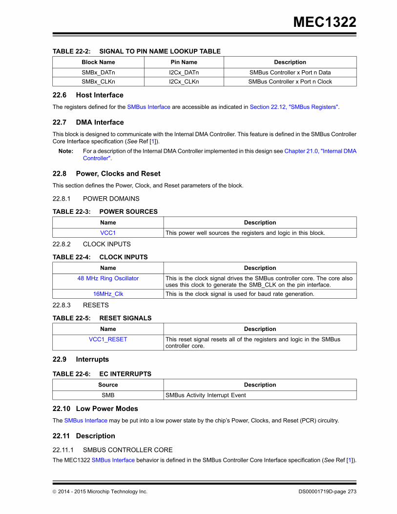
MEC1322
22.6 Host Interface
The registers defined for the SMBus Interface are accessible as indicated in Section 22.12, "SMBus Registers".
22.7 DMA Interface
This block is designed to communicate with the Internal DMA Controller. This feature is defined in the SMBus ControllerCore Interface specification (See Ref [1]).
Note: For a description of the Internal DMA Controller implemented in this design see Chapter 21.0, "Internal DMAController".
22.8 Power, Clocks and Reset
This section defines the Power, Clock, and Reset parameters of the block.
22.8.1 POWER DOMAINS
22.8.2 CLOCK INPUTS
22.8.3 RESETS
22.9 Interrupts
22.10 Low Power Modes
The SMBus Interface may be put into a low power state by the chip’s Power, Clocks, and Reset (PCR) circuitry.
22.11 Description
22.11.1 SMBUS CONTROLLER CORE
The MEC1322 SMBus Interface behavior is defined in the SMBus Controller Core Interface specification (See Ref [1]).
TABLE 22-2: SIGNAL TO PIN NAME LOOKUP TABLE
Block Name Pin Name Description
SMBx_DATn I2Cx_DATn SMBus Controller x Port n Data
SMBx_CLKn I2Cx_CLKn SMBus Controller x Port n Clock
TABLE 22-3: POWER SOURCES
Name Description
VCC1 This power well sources the registers and logic in this block.
TABLE 22-4: CLOCK INPUTS
Name Description
48 MHz Ring Oscillator This is the clock signal drives the SMBus controller core. The core also uses this clock to generate the SMB_CLK on the pin interface.
16MHz_Clk This is the clock signal is used for baud rate generation.
TABLE 22-5: RESET SIGNALS
Name Description
VCC1_RESET This reset signal resets all of the registers and logic in the SMBus controller core.
TABLE 22-6: EC INTERRUPTS
Source Description
SMB SMBus Activity Interrupt Event
2014 - 2015 Microchip Technology Inc. DS00001719D-page 273

MEC1322
22.11.2 PHYSICAL INTERFACE
The SMBus Interface has two physical ports, selected by the PORT SEL [3:0] bits in the Configuration Register asdescribed in Ref [1].
Note 1: SMBus controller 0 uses port 0 and port 1. SMBus controllers 1-3 use port 0.
2: The buffer type for these pins must be configured as open-drain outputs in the GPIO Configuration registersassociated with the GPIO signals that share the ports.
22.12 SMBus Registers
The registers listed in the SMBus Core Register Summary table in the SMBus Controller Core Interface specification(Ref [1]) are for a single instance of the SMBus Controller Core. The addresses of each register listed in this table aredefined as a relative offset to the host “Base Address” defined in the following table:
Note 22-1 The Base Address indicates where the first register can be accessed in a particular address spacefor a block instance.
TABLE 22-7: EC-ONLY REGISTER BASE ADDRESS TABLE
Block InstanceInstance Number
Host Address Space Base Address (Note 22-1)
SMBus Controller 0 EC 32-bit internal address space
4000_1800h
SMBus Controller 1 EC 32-bit internal address space
4000_AC00h
SMBus Controller 2 EC 32-bit internal address space
4000_B000h
SMBus Controller 3 EC 32-bit internal address space
4000_B400h
DS00001719D-page 274 2014 - 2015 Microchip Technology Inc.
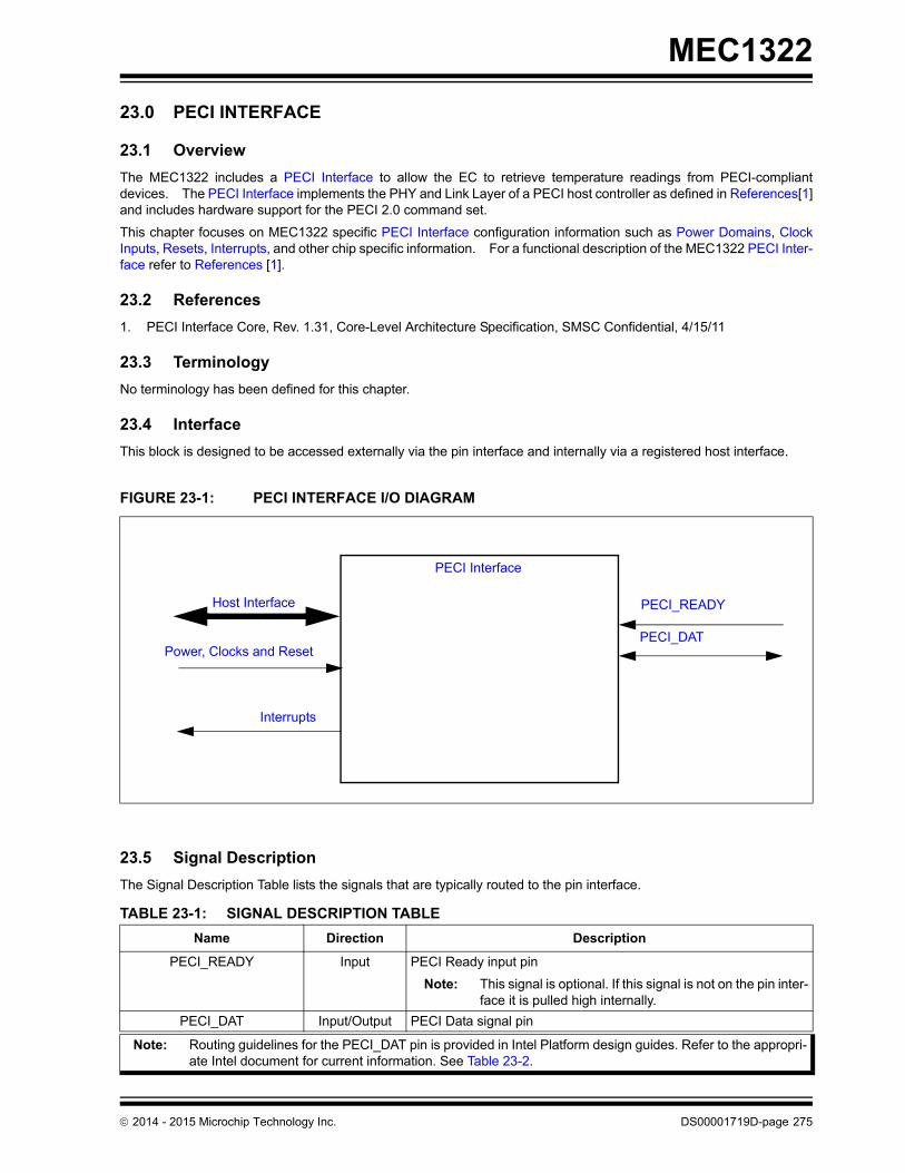
MEC1322
23.0 PECI INTERFACE
23.1 Overview
The MEC1322 includes a PECI Interface to allow the EC to retrieve temperature readings from PECI-compliantdevices. The PECI Interface implements the PHY and Link Layer of a PECI host controller as defined in References[1]and includes hardware support for the PECI 2.0 command set.
This chapter focuses on MEC1322 specific PECI Interface configuration information such as Power Domains, ClockInputs, Resets, Interrupts, and other chip specific information. For a functional description of the MEC1322 PECI Inter-face refer to References [1].
23.2 References
1. PECI Interface Core, Rev. 1.31, Core-Level Architecture Specification, SMSC Confidential, 4/15/11
23.3 Terminology
No terminology has been defined for this chapter.
23.4 Interface
This block is designed to be accessed externally via the pin interface and internally via a registered host interface.
23.5 Signal Description
The Signal Description Table lists the signals that are typically routed to the pin interface.
FIGURE 23-1: PECI INTERFACE I/O DIAGRAM
TABLE 23-1: SIGNAL DESCRIPTION TABLE
Name Direction Description
PECI_READY Input PECI Ready input pin
Note: This signal is optional. If this signal is not on the pin inter-face it is pulled high internally.
PECI_DAT Input/Output PECI Data signal pin
Note: Routing guidelines for the PECI_DAT pin is provided in Intel Platform design guides. Refer to the appropri-ate Intel document for current information. See Table 23-2.
PECI_READY
PECI_DAT
PECI Interface
Power, Clocks and Reset
Interrupts
Host Interface
2014 - 2015 Microchip Technology Inc. DS00001719D-page 275

MEC1322
23.6 Host Interface
The registers defined for the PECI Interface are accessible by the various hosts as indicated in Section 23.11, "PECIInterface Registers".
23.7 Power, Clocks and Reset
This section defines the Power, Clock, and Reset parameters of the block.
23.7.1 POWER DOMAINS
23.7.2 CLOCK INPUTS
23.7.3 RESETS
23.8 Interrupts
This section defines the Interrupt Sources generated from this block.
23.9 Low Power Modes
The PECI Interface may be put into a low power state by the chip’s Power, Clocks, and Reset (PCR) circuitry.
23.10 Instance Description
There is one instance of the PECI Core implemented in the PECI Interface in the MEC1322. See PECI Interface Core,Rev. 1.31, Core-Level Architecture Specification, SMSC Confidential, 4/15/11 for a description of the PECI Core.
23.11 PECI Interface Registers
The registers listed in the PECI Interface Register Summary table are for a single instance of the PECI Interface. Theaddresses of each register listed in this table are defined as a relative offset to the host “Base Address” defined in thePECI Interface Register Base Address Table.
TABLE 23-2: PECI ROUTING GUIDELINES
Trace Impedance 50 Ohms +/- 15%
Spacing 10 mils
Routing Layer Microstrip
Trace Width Calculate to match impedance
Length 1” - 15”
TABLE 23-3: POWER SOURCES
Name Description
VCC1 The PECI Interface logic and registers are powered by VCC1.
TABLE 23-4: CLOCK INPUTS
Name Description
48 MHz Ring Oscillator PECI Module Input Clock
TABLE 23-5: RESET SIGNALS
Name Description
VCC1_RESET PECI Core Reset Input
TABLE 23-6: EC INTERRUPTS
Source Description
PECIHOST PECI Host
DS00001719D-page 276 2014 - 2015 Microchip Technology Inc.
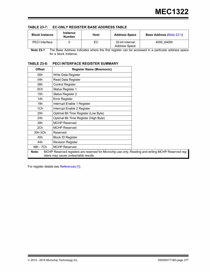
MEC1322
Note 23-1 The Base Address indicates where the first register can be accessed in a particular address spacefor a block instance.
For register details see References [1].
TABLE 23-7: EC-ONLY REGISTER BASE ADDRESS TABLE
Block InstanceInstance Number
Host Address Space Base Address (Note 23-1)
PECI Interface 0 EC 32-bit Internal Address Space
4000_6400h
TABLE 23-8: PECI INTERFACE REGISTER SUMMARY
Offset Register Name (Mnemonic)
00h Write Data Register
04h Read Data Register
08h Control Register
0Ch Status Register 1
10h Status Register 2
14h Error Register
18h Interrupt Enable 1 Register
1Ch Interrupt Enable 2 Register
20h Optimal Bit Time Register (Low Byte)
24h Optimal Bit Time Register (High Byte)
28h MCHP Reserved
2Ch MCHP Reserved
30h-3Ch Reserved
40h Block ID Register
44h Revision Register
48h - 7Ch MCHP Reserved
Note: MCHP Reserved registers are reserved for Microchip use only. Reading and writing MCHP Reserved reg-isters may cause undesirable results
2014 - 2015 Microchip Technology Inc. DS00001719D-page 277

MEC1322
24.0 TACH
24.1 Introduction
This block monitors TACH output signals (or locked rotor signals) from various types of fans, and determines theirspeed.
24.2 References
No references have been cited for this feature.
24.3 Terminology
There is no terminology defined for this section.
24.4 Interface
This block is designed to be accessed externally via the pin interface and internally via a registered host interface.
24.5 Signal Description
24.6 Host Interface
The registers defined for the TACH are accessible by the various hosts as indicated in Section 24.11, "EC-Only Regis-ters".
FIGURE 24-1: I/O DIAGRAM OF BLOCK
TABLE 24-1: SIGNAL DESCRIPTION TABLE
Name Direction Description
TACH INPUT Input Tachometer signal from TACHx Pin.
Signal Description
TACH
Interrupts
Power, Clocks and Reset
Host Interface
DS00001719D-page 278 2014 - 2015 Microchip Technology Inc.
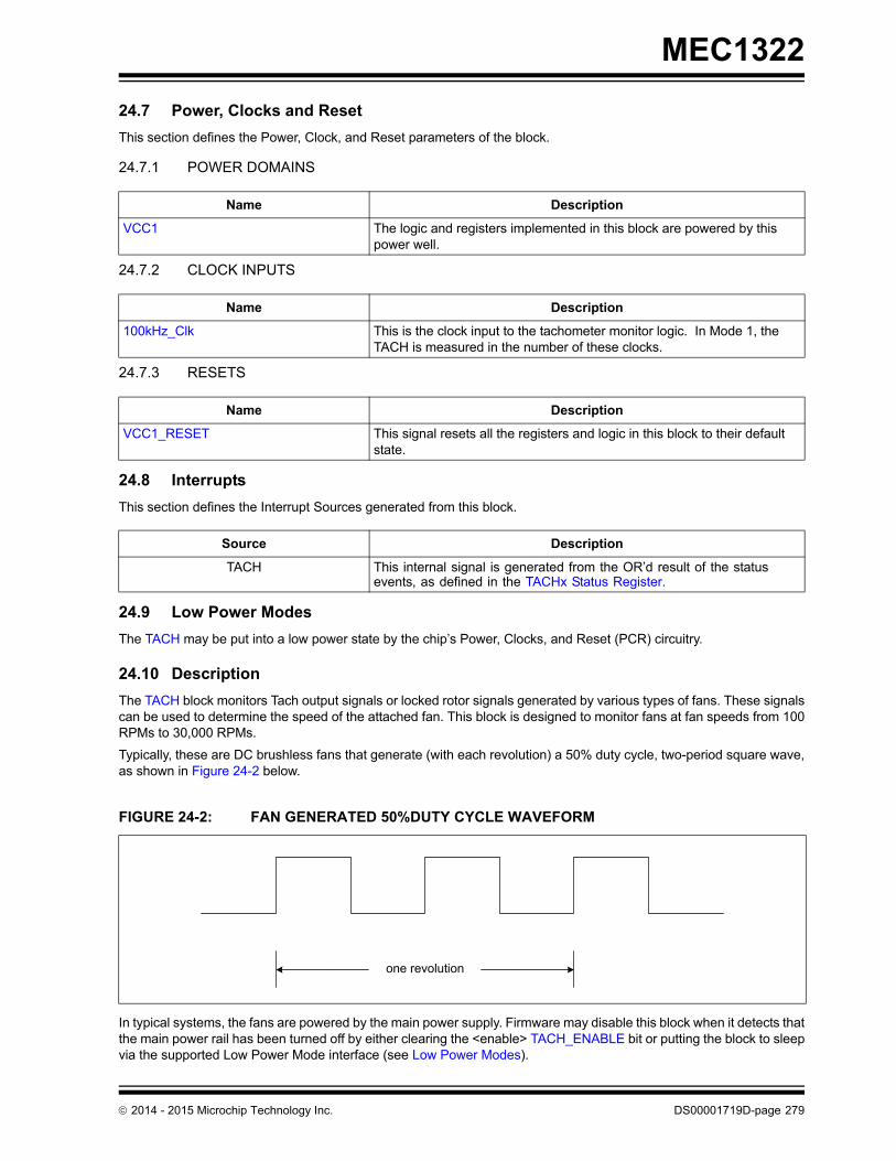
MEC1322
24.7 Power, Clocks and Reset
This section defines the Power, Clock, and Reset parameters of the block.
24.7.1 POWER DOMAINS
24.7.2 CLOCK INPUTS
24.7.3 RESETS
24.8 Interrupts
This section defines the Interrupt Sources generated from this block.
24.9 Low Power Modes
The TACH may be put into a low power state by the chip’s Power, Clocks, and Reset (PCR) circuitry.
24.10 Description
The TACH block monitors Tach output signals or locked rotor signals generated by various types of fans. These signalscan be used to determine the speed of the attached fan. This block is designed to monitor fans at fan speeds from 100RPMs to 30,000 RPMs.
Typically, these are DC brushless fans that generate (with each revolution) a 50% duty cycle, two-period square wave,as shown in Figure 24-2 below.
In typical systems, the fans are powered by the main power supply. Firmware may disable this block when it detects thatthe main power rail has been turned off by either clearing the <enable> TACH_ENABLE bit or putting the block to sleepvia the supported Low Power Mode interface (see Low Power Modes).
Name Description
VCC1 The logic and registers implemented in this block are powered by this power well.
Name Description
100kHz_Clk This is the clock input to the tachometer monitor logic. In Mode 1, the TACH is measured in the number of these clocks.
Name Description
VCC1_RESET This signal resets all the registers and logic in this block to their default state.
Source Description
TACH This internal signal is generated from the OR’d result of the status events, as defined in the TACHx Status Register.
FIGURE 24-2: FAN GENERATED 50%DUTY CYCLE WAVEFORM
one revolution
2014 - 2015 Microchip Technology Inc. DS00001719D-page 279

MEC1322
24.10.1 MODES OF OPERATION
The Tachometer block supports two modes of operation. The mode of operation is selected via the TACH_READING_-MODE_SELECT bit.
24.10.1.1 Free Running Counter
In Mode 0, the Tachometer block uses the TACH input as the clock source for the internal TACH pulse counter (seeTACHX_COUNTER). The counter is incremented when it detects a rising edge on the TACH input. In this mode, thefirmware may periodically poll the TACHX_COUNTER field to determine the average speed over a period of time. Thefirmware must store the previous reading and the current reading to compute the number of pulses detected over aperiod of time. In this mode, the counter continuously increments until it reaches FFFFh. It then wraps back to 0000hand continues counting. The firmware must ensure that the sample rate is greater than the time it takes for the counterto wrap back to the starting point.
24.10.1.2 Mode 1 -- Number of Clock Pulses per Revolution
In Mode 1, the Tachometer block uses its 100kHz_Clk clock input to measure the programmable number of TACHpulses. In this mode, the internal TACH pulse counter (TACHX_COUNTER) returns the value in number of 100kHz_Clkpulses per programmed number of TACH_EDGES. For fans that generate two square waves per revolution, these bitsshould be configured to five edges.
When the number of edges is detected, the counter is latched and the COUNT_READY_STATUS bit is asserted. If theCOUNT_READY_INT_EN bit is set a TACH interrupt event will be generated.
24.10.2 OUT-OF-LIMIT EVENTS
The TACH Block has a pair of limit registers that may be configured to generate an event if the Tach indicates that thefan is operating too slow or too fast. If the <TACH reading> exceeds one of the programmed limits, the TACHx HighLimit Register and the TACHx Low Limit Register, the bit TACH_OUT_OF_LIMIT_STATUS will be set. If theTACH_OUT_OF_LIMIT_STATUS bit is set, the Tachometer block will generate an interrupt event.
24.11 EC-Only Registers
The registers listed in the EC-Only Register Summary table are for a single instance of the TACH. The addresses ofeach register listed in this table are defined as a relative offset to the host “Base Address” defined in the EC-Only Reg-ister Base Address Table.
The Base Address indicates where the first register can be accessed in a particular address space for a block instance.
Note: Tach interrupts should be disabled in Mode 0.
TABLE 24-2: EC-ONLY REGISTER BASE ADDRESS TABLE
Block InstanceInstance Number Host Address Space Base Address
TACH 0 EC 32-bit internal address space
4000_6000h
TACH 1 EC 32-bit internal address space
4000_6010h
TABLE 24-3: TACH REGISTER SUMMARY
Offset Register Name (Mnemonic)
00h TACHx Control Register
04h TACHx Status Register
08h TACHx High Limit Register
0Ch TACHx Low Limit Register
DS00001719D-page 280 2014 - 2015 Microchip Technology Inc.

MEC1322
24.11.1 TACHX CONTROL REGISTER
Offset 00h
Bits Description Type DefaultReset Event
31:16 TACHX_COUNTER
This 16-bit field contains the latched value of the internal Tach pulse counter, which may be configured by the Tach Reading Mode Select field to operate as a free-running counter or to be gated by the Tach input signal.
If the counter is free-running (Mode 0), the internal Tach counter increments (if enabled) on transitions of the raw Tach input signal and is latched into this field every time it is incremented. The act of reading this field will not reset the counter, which rolls over to 0000h after FFFFh. The firmware will compute the delta between the current count reading and the previous count reading, to determine the num-ber of pulses detected over a programmed period.
If the counter is gated by the Tach input and clocked by 100kHz_Clk (Mode 1), the internal counter will be latched into the reading register when the programmed number of edges is detected or when the counter reaches FFFFh. The internal counter is reset to zero after it is copied into this register.
Note: In Mode 1, a counter value of FFFFh means that the Tachdid not detect the programmed number of edges in655ms. A stuck fan can be detected by setting the TACHxHigh Limit Register to a number less than FFFFh. If theinternal counter then reaches FFFFh, the reading registerwill be set to FFFFh and an out-of-limit interrupt can besent to the EC.
R 00h VCC1_RESET
15 TACH_INPUT_INT_EN
1=Enable Tach Input toggle interrupt from Tach block0=Disable Tach Input toggle interrupt from Tach block
R/W 0b VCC1_RESET
14 COUNT_READY_INT_EN
1=Enable Count Ready interrupt from Tach block0=Disable Count Ready interrupt from Tach block
R/W 0b VCC1_RESET
13 Reserved R - -
12:11 TACH_EDGES
A Tach signal is a square wave with a 50% duty cycle. Typically, two Tach periods represents one revolution of the fan. A Tach period con-sists of three Tach edges.
This programmed value represents the number of Tach edges that will be used to determine the interval for which the number of 100kHz_Clk pulses will be counted
11b=9 Tach edges (4 Tach periods)10b=5 Tach edges (2 Tach periods)01b=3 Tach edges (1 Tach period)00b=2 Tach edges (1/2 Tach period)
R/W 00b VCC1_RESET
2014 - 2015 Microchip Technology Inc. DS00001719D-page 281

MEC1322
10 TACH_READING_MODE_SELECT
1=Counter is incremented on the rising edge of the 100kHz_Clk input.The counter is latched into the TACHX_COUNTER field andreset when the programmed number of edges is detected.
0=Counter is incremented when Tach Input transitions from low-to-high state (default)
R/W 0b VCC1_RESET
9 Reserved R - -
8 FILTER_ENABLE
This filter is used to remove high frequency glitches from Tach Input. When this filter is enabled, Tach input pulses less than two 100kHz_-Clk periods wide get filtered.
1= Filter enabled0= Filter disabled (default)
It is recommended that the Tach input filter always be enabled.
R/W 0b VCC1_RESET
7:2 Reserved R - -
1 TACH_ENABLE
This bit gates the clocks into the block. When clocks are gated, the TACHx pin is tristated. When re-enabled, the internal counters will continue from the last known state and stale status events may still be pending. Firmware should discard any status or reading values until the reading value has been updated at least one time after the enable bit is set.
1= TACH Monitoring enabled, clocks enabled.0= TACH Idle, clocks gated
R/W 0b VCC1_RESET
0 TACH_OUT_OF_LIMIT_ENABLE
This bit is used to enable the TACH_OUT_OF_LIMIT_STATUS bit in the TACHx Status Register to generate an interrupt event.
1=Enable interrupt output from Tach block0=Disable interrupt output from Tach block (default)
R/W 0b VCC1_RESET
Offset 00h
Bits Description Type DefaultReset Event
DS00001719D-page 282 2014 - 2015 Microchip Technology Inc.

MEC1322
24.11.2 TACHX STATUS REGISTER
Note 1: Some fans offer a Locked Rotor output pin that generates a level event if a locked rotor is detected. This bitmay be used in combination with the Tach pin status bit to detect a locked rotor signal event from a fan.
2: Tach Input may come up as active for Locked Rotor events. This would not cause an interrupt event becausethe pin would not toggle. Firmware must read the status events as part of the initialization process, if pollingis not implemented.
Offset 04h
Bits Description Type DefaultReset Event
31:4 Reserved R - -
3 COUNT_READY_STATUS
This status bit is asserted when the Tach input changes state and when the counter value is latched. This bit remains cleared to '0' when the TACH_READING_MODE_SELECT bit in the TACHx Con-trol Register is '0'.When the TACH_READING_MODE_SELECT bit in the TACHx Con-trol Register is set to '1', this bit is set to ‘1’ when the counter value is latched by the hardware. It is cleared when written with a ‘1’. If COUNT_READY_INT_EN in the TACHx Control Register is set to 1, this status bit will assert the Tach Interrupt signal.
1=Reading ready0=Reading not ready
R/WC 0b VCC1_RESET
2 TOGGLE_STATUS
This bit is set when Tach Input changes state. It is cleared when writ-ten with a ’1’. If TACH_INPUT_INT_EN in the TACHx Control Regis-ter is set to ’1’, this status bit will assert the Tach Interrupt signal.
1=Tach Input changed state (this bit is set on a low-to-high or high-to-low transition)
0=Tach stable
R/WC 0b VCC1_RESET
1 TACH_PIN_STATUS
This bit reflects the state of Tach Input. This bit is a read only bit that may be polled by the embedded controller.
1= Tach Input is high0= Tach Input is low
R 0b VCC1_RESET
0 TACH_OUT_OF_LIMIT_STATUS
This bit is set when the Tach Count value is greater than the high limit or less than the low limit. It is cleared when written with a ’1’. To disable this status event set the limits to their extreme values. If TACH_OUT_OF_LIMIT_ENABLE in the TACHx Control Register is set to 1’, this status bit will assert the Tach Interrupt signal.
1=Tach is outside of limits0=Tach is within limits
R/WC 0b VCC1_RESET
2014 - 2015 Microchip Technology Inc. DS00001719D-page 283
MEC1322
24.11.3 TACHX HIGH LIMIT REGISTER
24.11.4 TACHX LOW LIMIT REGISTER
Offset 08h
Bits Description Type DefaultReset Event
31:16 Reserved - - -
15:0 TACH_HIGH_LIMIT
This value is compared with the value in the TACHX_COUNTER field. If the value in the counter is greater than the value programmed in this register, the TACH_OUT_OF_LIMIT_STATUS bit will be set. The TACH_OUT_OF_LIMIT_STATUS status event may be enabled to generate an interrupt to the embedded controller via the TACH_OUT_OF_LIMIT_ENABLE bit in the TACHx Control Register.
R/W FFFFh VCC1_RESET
Offset 0Ch
Bits Description Type DefaultReset Event
31:16 Reserved R - -
15:0 TACHX_LOW_LIMIT
This value is compared with the value in the TACHX_COUNTER field of the TACHx Control Register. If the value in the counter is less than the value programmed in this register, the TACH_OUT_OF_LIM-IT_STATUS bit will be set. The TACH_OUT_OF_LIMIT_STATUS sta-tus event may be enabled to generate an interrupt to the embedded controller via the TACH_OUT_OF_LIMIT_ENABLE bit in the TACHx Control Register
To disable the TACH_OUT_OF_LIMIT_STATUS low event, program 0000h into this register.
R/W 0000h VCC1_RESET
DS00001719D-page 284 2014 - 2015 Microchip Technology Inc.

MEC1322
25.0 PWM
25.1 Introduction
This block generates a PWM output that can be used to control 4-wire fans, blinking LEDs, and other similar devices.Each PWM can generate an arbitrary duty cycle output at frequencies from less than 0.1 Hz to 24 MHz. The PWM con-troller can also used to generate the PROCHOT output and Speaker output.
The PWMx Counter ON Time registers and PWMx Counter OFF Time registers determine the operation of thePWM_OUTPUT signals. See Section 25.11.1, "PWMx Counter ON Time Register," on page 288 and Section 25.11.2,"PWMx Counter OFF Time Register," on page 289 for a description of the PWM_OUTPUT signals.
25.2 References
There are no standards referenced in this chapter.
25.3 Terminology
There is no terminology defined for this section.
25.4 Interface
This block is designed to be accessed externally via the pin interface and internally via a registered host interface.
There are no external signals for this block.
FIGURE 25-1: I/O DIAGRAM OF BLOCK
PWM
Interrupts
Power, Clocks and Reset
Host Interface
Signal Description
2014 - 2015 Microchip Technology Inc. DS00001719D-page 285

MEC1322
25.5 Signal Description
25.6 Host Interface
The registers defined for the PWM Interface are accessible by the various hosts as indicated in Section 25.11, "EC-OnlyRegisters".
25.7 Power, Clocks and Reset
This section defines the Power, Clock, and Reset parameters of the block.
25.7.1 POWER DOMAINS
25.7.2 CLOCK INPUTS
25.7.3 RESETS
25.8 Interrupts
The PWM block does not generate any interrupt events.
25.9 Low Power Modes
The PWM may be put into a low power state by the chip’s Power, Clocks, and Reset (PCR) circuitry. When the PWM isin the sleep state, the internal counters reset to 0 and the internal state of the PWM and the PWM_OUTPUT signal setto the OFF state.
25.10 Description
The PWM_OUTPUT signal is used to generate a duty cycle of specified frequency. This block can be programmed sothat the PWM signal toggles the PWM_OUTPUT, holds it high, or holds it low. When the PWM is configured to toggle,the PWM_OUTPUT alternates from high to low at the rate specified in the PWMx Counter ON Time Register and PWMxCounter OFF Time Register.
The following diagram illustrates how the clock inputs and registers are routed to the PWM Duty Cycle & FrequencyControl logic to generate the PWM output.
TABLE 25-1: SIGNAL DESCRIPTION TABLE
Name Direction Description
PWM_OUTPUT OUTPUT Pulse Width Modulated signal to PWMx pin.
TABLE 25-2: POWER SOURCES
Name Description
VCC1 The PWM logic and registers are powered by this single power source.
TABLE 25-3: CLOCK INPUTS
Name Description
100kHz_Clk 100kHz_Clk clock input for generating low PWM frequencies, such as 10 Hz to 100 Hz.
48 MHz Ring Oscillator 48 MHz Ring Oscillator clock input for generating high PWM frequencies, such as 15 kHz to 30 kHz.
TABLE 25-4: RESET SIGNALS
Name Description
VCC1_RESET This reset signal resets all the logic in this block to its initial state including the registers, which are set to their defined default state.
DS00001719D-page 286 2014 - 2015 Microchip Technology Inc.
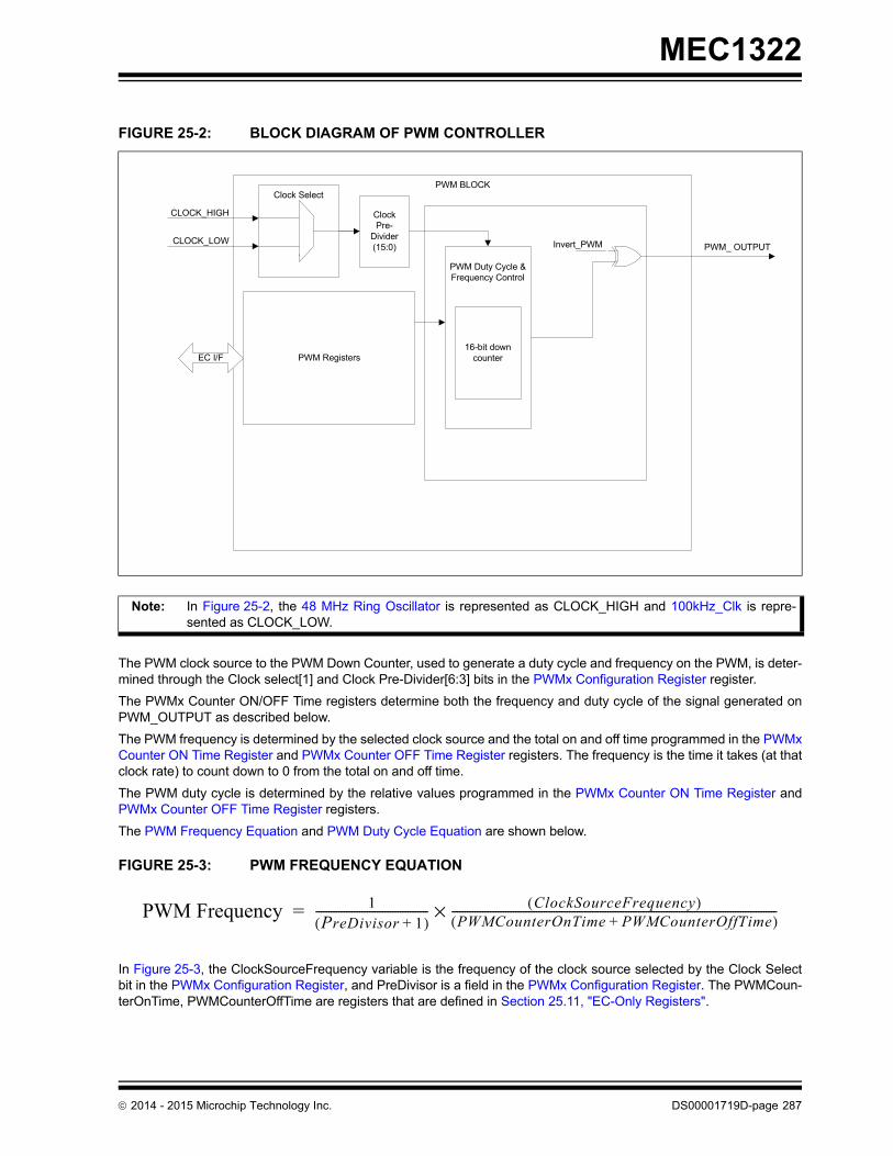
MEC1322
The PWM clock source to the PWM Down Counter, used to generate a duty cycle and frequency on the PWM, is deter-mined through the Clock select[1] and Clock Pre-Divider[6:3] bits in the PWMx Configuration Register register.
The PWMx Counter ON/OFF Time registers determine both the frequency and duty cycle of the signal generated onPWM_OUTPUT as described below.
The PWM frequency is determined by the selected clock source and the total on and off time programmed in the PWMxCounter ON Time Register and PWMx Counter OFF Time Register registers. The frequency is the time it takes (at thatclock rate) to count down to 0 from the total on and off time.
The PWM duty cycle is determined by the relative values programmed in the PWMx Counter ON Time Register andPWMx Counter OFF Time Register registers.
The PWM Frequency Equation and PWM Duty Cycle Equation are shown below.
FIGURE 25-3: PWM FREQUENCY EQUATION
In Figure 25-3, the ClockSourceFrequency variable is the frequency of the clock source selected by the Clock Selectbit in the PWMx Configuration Register, and PreDivisor is a field in the PWMx Configuration Register. The PWMCoun-terOnTime, PWMCounterOffTime are registers that are defined in Section 25.11, "EC-Only Registers".
FIGURE 25-2: BLOCK DIAGRAM OF PWM CONTROLLER
Note: In Figure 25-2, the 48 MHz Ring Oscillator is represented as CLOCK_HIGH and 100kHz_Clk is repre-sented as CLOCK_LOW.
PWM BLOCK
PWM Duty Cycle & Frequency Control
PWM_ OUTPUT
PWM Registers
CLOCK_HIGH
CLOCK_LOW Invert_PWM
Clock Select
16-bit down counterEC I/F
Clock Pre-
Divider(15:0)
PWM Frequency 1PreDivisor 1+( )
-------------------------------------------- ClockSourceFrequency( )PWMCounterOnTime PWMCounterOffTime+( )
-------------------------------------------------------------------------------------------------------------------------------×=
2014 - 2015 Microchip Technology Inc. DS00001719D-page 287

MEC1322
FIGURE 25-4: PWM DUTY CYCLE EQUATION
The PWMx Counter ON Time Register and PWMx Counter OFF Time Register registers should be accessed as 16-bitvalues.
25.11 EC-Only Registers
The registers listed in the EC-Only Register Summary table are for a single instance of the PWM. The addresses ofeach register listed in this table are defined as a relative offset to the host “Base Address” defined in the EC-Only Reg-ister Base Address Table.
The Base Address indicates where the first register can be accessed in a particular address space for a block instance.
25.11.1 PWMX COUNTER ON TIME REGISTER
TABLE 25-5: EC-ONLY REGISTER BASE ADDRESS TABLE
Block InstanceInstance Number Host Address Space Base Address
PWM 0 EC 32-bit internal address space
4000_5800h
PWM 1 EC 32-bit internal address space
4000_5810h
PWM 2 EC 32-bit internal address space
4000_5820h
PWM 3 EC 32-bit internal address space
4000_5830h
TABLE 25-6: EC-ONLY REGISTER SUMMARY
Offset Register Name (Mnemonic)
00h PWMx Counter ON Time Register
04h PWMx Counter OFF Time Register
08h PWMx Configuration Register
Offset 00h
Bits Description Type DefaultReset Event
31:16 Reserved R - -
15:0 PWMX_COUNTER_ON_TIME
This field determine both the frequency and duty cycle of the PWM signal.When this field is set to zero and the PWMX_COUNTER_OFF_-TIME is not set to zero, the PWM_OUTPUT is held low (Full Off).
R/W 0000h VCC1_RESET
PWM Duty Cycle PWMCounterOnTimePWMCounterOnTime PWMCounterOffTime+( )
--------------------------------------------------------------------------------------------------------------------------------=
DS00001719D-page 288 2014 - 2015 Microchip Technology Inc.

MEC1322
25.11.2 PWMX COUNTER OFF TIME REGISTER
25.11.3 PWMX CONFIGURATION REGISTER
Offset 04h
Bits Description Type DefaultReset Event
31:16 Reserved R - -
15:0 PWMX_COUNTER_OFF_TIME
This field determine both the frequency and duty cycle of the PWM signal.When this field is set to zero, the PWM_OUTPUT is held high (Full On).
R/W FFFFh VCC1_RESET
Offset 08h
Bits Description Type DefaultReset Event
31:7 Reserved R - -
6:3 CLOCK_PRE_DIVIDERThe Clock source for the 16-bit down counter (see PWMx Counter ON Time Register and PWMx Counter OFF Time Register) is deter-mined by bit D1 of this register. The Clock source is then divided by the value of Pre-Divider+1 and the resulting signal determines the rate at which the down counter will be decremented. For example, a Pre-Divider value of 1 divides the input clock by 2 and a value of 2 divides the input clock by 3. A Pre-Divider of 0 will disable the Pre-Divider option.
R/W 0000b VCC1_RESET
2 INVERT
1= PWM_OUTPUT ON State is active low0=PWM_OUTPUT ON State is active high
R/W 0b VCC1_RESET
1 CLOCK_SELECTThis bit determines the clock source used by the PWM duty cycle and frequency control logic.
1=CLOCK_LOW0=CLOCK_HIGH
R/W 0b VCC1_RESET
0 PWM_ENABLE
1=Enabled (default)0=Disabled (gates clocks to save power)
Note: When the PWM enable bit is set to 0 the internal countersare reset and the internal state machine is set to the OFFstate. In addition, the PWM_OUTPUT signal is set to theinactive state as determined by the Invert bit. The PWMxCounter ON Time Register and PWMx Counter OFFTime Register are not affected by the PWM enable bitand may be read and written while the PWM enable bit is0.
R/W 0b VCC1_RESET
2014 - 2015 Microchip Technology Inc. DS00001719D-page 289

MEC1322
26.0 RPM-PWM INTERFACE
26.1 Introduction
The RPM-PWM Interface is closed-loop RPM based Fan Control Algorithm that monitors the fan’s speed and automat-ically adjusts the drive to maintain the desired fan speed.
The RPM-PWM Interface functionality consists of a closed-loop “set-and-forget” RPM based fan controller.
26.2 References
No references have been cited for this chapter
26.3 Terminology
There is no terminology defined for this chapter.
26.4 Interface
This block is designed to be accessed externally via the pin interface and internally via a registered host interface.
The registers in the block are accessed by embedded controller code at the addresses shown in Section 26.9, "FanControl Register Bank".
Figure 26-1 illustrates and categorizes the RPM-PWM Interface block signals. These signals are described in Table 26-1.
26.4.1 FAN CONTROL
The Fan Control Signal Description Table lists the signals that are routed to/from the block.
26.4.2 HOST INTERFACE
The registers defined for the RPM-PWM Interface are accessible by the various hosts as indicated in Section 26.9, "FanControl Register Bank".
FIGURE 26-1: RPM-PWM INTERFACE I/O DIAGRAM
TABLE 26-1: FAN CONTROL SIGNAL DESCRIPTION TABLE
Name Direction Description
TACH Input Tachometer input from fan
PWM Output PWM fan drive output
RPM-PWM Interface
Power, Clocks and Reset
Interrupts
Host Interface
Fan Control
DS00001719D-page 290 2014 - 2015 Microchip Technology Inc.
MEC1322
26.5 Power, Clocks and Reset
This section defines the Power, Clock, and Reset parameters of the block.
26.5.1 POWER DOMAINS
26.5.2 CLOCK INPUTS
26.5.3 RESETS
26.6 Interrupts
This section defines the Interrupt Sources generated from this block.
26.7 Low Power Modes
The RPM-PWM Interface may be put into a low power state by the chip’s Power, Clocks, and Reset (PCR) circuitry.
26.8 Description
This section defines the functionality of the block.
26.8.1 GENERAL OPERATION
The RPM-PWM Interface is an RPM based Fan Control Algorithm that monitors the fan’s speed and automaticallyadjusts the drive to maintain the desired fan speed. This RPM based Fan Control Algorithm controls a PWM outputbased on a tachometer input.
26.8.2 FAN CONTROL MODES OF OPERATION
The RPM-PWM Interface has two modes of operation for the PWM Fan Driver. They are:
1. Manual Mode - in this mode of operation, the user directly controls the fan drive setting. Updating the Fan DriverSetting Register (see Section 26.9.1, "Fan Setting Register") will update the fan drive based on the programmedramp rate (default disabled).
• The Manual Mode is enabled by clearing the EN_ALGO bit in the Fan Configuration Register (see Section 26.9.3, "Fan Configuration 1 Register").
• Whenever the Manual Mode is enabled the current drive settings will be changed to what was last used by the RPM control algorithm.
• Setting the drive value to 00h will disable the PWM Fan Driver.
• Changing the drive value from 00h will invoke the Spin Up Routine.
TABLE 26-2: POWER SOURCES
Name Description
VCC1 This power well sources the registers and logic in this block.
TABLE 26-3: CLOCK INPUTS
Name Description
48 MHz Ring Oscillator This clock signal drives selected logic (e.g., counters).
TABLE 26-4: RESET SIGNALS
Name Description
VCC1_RESET This reset signal resets all of the registers and logic in this block.
TABLE 26-5: INTERRUPTS
Source Description
Fan Fail/Spin Status Interrupt The DRIVE_FAIL & FAN_SPIN bits in the Fan Status Register are logi-cally ORed and routed to the FAIL_SPIN Interrupt
Fan Stall Status Interrupt The FAN_STALL bit in the Fan Status Register is routed to the FAN_STALL Interrupt
2014 - 2015 Microchip Technology Inc. DS00001719D-page 291

MEC1322
2. Using RPM based Fan Control Algorithm - in this mode of operation, the user determines a target tachometerreading and the drive setting is automatically updated to achieve this target speed.
26.8.3 RPM BASED FAN CONTROL ALGORITHM
The RPM-PWM Interface includes an RPM based Fan Control Algorithm.
The fan control algorithm uses Proportional, Integral, and Derivative terms to automatically approach and maintain thesystem’s desired fan speed to an accuracy directly proportional to the accuracy of the clock source. Figure 26-2, "RPMbased Fan Control Algorithm" shows a simple flow diagram of the RPM based Fan Control Algorithm operation.
The desired tachometer count is set by the user inputting the desired number of 32.768KHz cycles that occur per fanrevolution. The user may change the target count at any time. The user may also set the target count to FFh in order todisable the fan driver.
For example, if a desired RPM rate for a 2-pole fan is 3000 RPMs, the user would input the hexadecimal equivalent of1312d (52_00h in the TACH Target Registers). This number represents the number of 32.768KHz cycles that wouldoccur during the time it takes the fan to complete a single revolution when it is spinning at 3000RPMs (see Section26.9.11, "TACH Target Register" and Section 26.9.12, "TACH Reading Register").
The RPM-PWM Interface’s RPM based Fan Control Algorithm has programmable configuration settings for parameterssuch as ramp-rate control and spin up conditions. The fan driver automatically detects and attempts to alleviate astalled/stuck fan condition while also asserting the interrupt signal. The RPM-PWM Interface works with fans that oper-ate up to 16,000 RPMs and provide a valid tachometer signal. The fan controller will function either with an externallysupplied 32.768KHz clock source or with its own internal 32KHz oscillator depending on the required accuracy.
TABLE 26-6: FAN CONTROLS ACTIVE FOR OPERATING MODE
Manual Mode Algorithm
Fan Driver Setting (read / write) Fan Driver Setting (read only)
EDGES[1:0] (Fan Configuration) EDGES[1:0] (Fan Configuration)
UPDATE[2:0] (Fan configuration) UPDATE[2:0] (Fan configuration)
LEVEL (Spin Up Configuration) LEVEL (Spin Up Configuration)
SPINUP_TIME[1:0] (Spin Up Configuration) SPINUP_TIME[1:0] (Spin Up Configuration)
Fan Step Fan Step
- Fan Minimum Drive
Valid TACH Count Valid TACH Count
- TACH Target
TACH Reading TACH Reading
RANGE[2:0] (Fan Configuration 2) RANGE[2:0] (Fan Configuration 2)
- DRIVE_FAIL_CNT[2:0] (Spin Up Config) and Drive Fail Band
DS00001719D-page 292 2014 - 2015 Microchip Technology Inc.

MEC1322
FIGURE 26-2: RPM BASED FAN CONTROL ALGORITHM
26.8.3.1 Programming the RPM Based Fan Control Algorithm
The RPM based Fan Control Algorithm powers-up disabled. The following registers control the algorithm. The RPM-PWM Interface fan control registers are pre-loaded with defaults that will work for a wide variety of fans so only the TACHTarget Register is required to set a fan speed. The other fan control registers can be used to fine-tune the algorithmbehavior based on application requirements.
1. Set the Valid TACH Count Register to the minimum tachometer count that indicates the fan is spinning.
2. Set the Spin Up Configuration Register to the spin up level and Spin Time desired.
3. Set the Fan Step Register to the desired step size.
4. Set the Fan Minimum Drive Register to the minimum drive value that will maintain fan operation.
5. Set the Update Time, and Edges options in the Fan Configuration Register.
6. Set the TACH Target Register to the desired tachometer count.
7. Enable the RPM based Fan Control Algorithm by setting the EN_ALGO bit.
Set TACH Target Count
Measure Fan Speed
Perform Spin Up Routine
Maintain Fan Drive
Ramp Rate Control
Reduce Fan Drive Increase Fan Drive
Spin Up Required
?
TACH Reading=
TACH Target?
TACH Reading <
TACH Target?
Yes
No
No
No
Yes
Yes
2014 - 2015 Microchip Technology Inc. DS00001719D-page 293

MEC1322
26.8.3.2 Tachometer Measurement
In both modes of operation, the tachometer measurement operates independently of the mode of operation of the fandriver and RPM based Fan Speed Control algorithm. Any tachometer reading that is higher than the Valid TACH Count(see Section 26.9.9, "Valid TACH Count Register") will flag a stalled fan and trigger an interrupt.
When measuring the tachometer, the fan must provide a valid tachometer signal at all times to ensure proper operation.The tachometer measurement circuitry is programmable to detect the fan speed of a variety of fan configurations andarchitectures including 1-pole, 2-pole (default), 3-pole, and 4-pole fans.
APPLICATION NOTE: The tachometer measurement works independently of the drive settings. If the device is putinto manual mode and the fan drive is set at a level that is lower than the fan can operate(including zero drive), the tachometer measurement may signal a Stalled Fan condition andassert an interrupt.
STALLED FAN
If the TACH Reading Register exceeds the user-programmable Valid TACH Count setting, it will flag the fan as stalledand trigger an interrupt. If the RPM based Fan Control Algorithm is enabled, the algorithm will automatically attempt torestart the fan until it detects a valid tachometer level or is disabled.
The FAN_STALL Status bit indicates that a stalled fan was detected. This bit is checked conditionally depending on themode of operation.
• Whenever the Manual Mode is enabled or whenever the drive value is changed from 00h, the FAN_STALL inter-rupt will be masked for the duration of the programmed Spin Up Time (see Table 26-17, “Spin time,” on page 303) to allow the fan an opportunity to reach a valid speed without generating unnecessary interrupts.
• In Manual Mode, whenever the TACH Reading Register exceeds the Valid TACH Count Register setting, the FAN_STALL status bit will be set.
• When the RPM based Fan Control Algorithm, the stalled fan condition is checked whenever the Update Time is met and the fan drive setting is updated. It is not a continuous check.
26.8.3.3 Spin Up Routine
The RPM-PWM Interface also contains programmable circuitry to control the spin up behavior of the fan driver to ensureproper fan operation. The Spin Up Routine is initiated under the following conditions:
• The TACH Target High Byte Register value changes from a value of FFh to a value that is less than the Valid TACH Count (see Section 26.9.9, "Valid TACH Count Register").
• The RPM based Fan Control Algorithm’s measured tachometer reading is greater than the Valid TACH Count.
• When in Manual Mode, the Drive Setting changes from a value of 00h.
When the Spin Up Routine is operating, the fan driver is set to full scale for one quarter of the total user defined spin uptime. For the remaining spin up time, the fan driver output is set a a user defined level (30% to 65% drive).
After the Spin Up Routine has finished, the RPM-PWM Interface measures the tachometer. If the measured tachometerreading is higher than the Valid TACH Count Register setting, the FAN_SPIN status bit is set and the Spin Up Routinewill automatically attempt to restart the fan.
APPLICATION NOTE: When the device is operating in manual mode, the FAN_SPIN status bit may be set if thefan drive is set at a level that is lower than the fan can operate (excluding zero drive whichdisables the fan driver). If the FAN_SPIN interrupt is unmasked, this condition will trigger anerrant interrupt.
Figure 26-3, "Spin Up Routine" shows an example of the Spin Up Routine in response to a programmed fan speedchange based on the first condition above.
DS00001719D-page 294 2014 - 2015 Microchip Technology Inc.

MEC1322
FIGURE 26-3: SPIN UP ROUTINE
26.8.4 PWM DRIVER
The RPM-PWM Interface contains an optional, programmable 8-bit PWM driver which can serve as part of the RPMbased Fan Speed Control Algorithm or in Manual Mode.
When enabled, the PWM driver can operate in four programmable frequency bands. The lower frequency bands offerfrequencies in the range of 9.5Hz to 4.8kHz while the higher frequency options offer frequencies of 21Hz or 25.2kHz.
26.8.5 ALERTS AND LIMITS
Figure 26-4, "Interrupt Flow" shows the interactions of the interrupts for fan events.
If the Fan Driver detects a drive fail, spin-up or stall event, the interrupt signal will be asserted (if enabled).
All of these interrupts can be masked from asserting the interrupt signal individually. If any bit of either Status register isset, the interrupt signal will be asserted provided that the corresponding interrupt enable bit is set accordingly.
The Status register will be updated due to an active event, regardless of the setting of the individual enable bits. Oncea status bit has been set, it will remain set until the Status register bit is written to 1 (and the error condition has beenremoved).
If the interrupt signal is asserted, it will be cleared immediately if either the status or enable bit is cleared.
See Section 26.6, "Interrupts," on page 291.
100% (optional)
Prev Target Count = FFh
Update TimeSpin Up Time
¼ of Spin Up Time
Target Count Changed
Check TACH Target Count Reached
30% through 65%
Fan Step
Algorithm controlled drive
New Target Count
2014 - 2015 Microchip Technology Inc. DS00001719D-page 295

MEC1322
FIGURE 26-4: INTERRUPT FLOW
26.9 Fan Control Register Bank
The registers listed in the Table 26-8, "Fan Control Register Summary" are for a single instance of the RPM-PWM Inter-face block. The addresses of each register listed in this table are defined as a relative offset to the host “Base Address”defined in Table 26-7, "Fan Control Register Bank Base Address Table".
Note 26-1 The Base Address indicates where the first register can be accessed in a particular address spacefor a block instance.
TABLE 26-7: FAN CONTROL REGISTER BANK BASE ADDRESS TABLE
Instance NameInstance Number
Host Address Space Base Address (Note 26-1)
RPM-PWM Inter-face
0 EC 32-bit internal address space
4000_A000h
TABLE 26-8: FAN CONTROL REGISTER SUMMARY
Register Name Offset
Fan Setting 00h
PWM Divide 01h
Fan Configuration 1 02h
Fan Configuration 2 03h
MCHP Reserved 04h
Gain 05h
Fan Spin Up Configuration 06h
Fan Step 07h
Fan Minimum Drive 08h
Valid Tach Count 09h
Fan Drive Fail Band Low Byte 0Ah
Fan Drive Fail Band High Byte 0Bh
Tach Target Low Byte 0Ch
Tach Target High Byte 0Dh
Tach Reading Low Byte 0Eh
Interrupt Status Bit 1
Interrupt Enable Bit 1
Interrupt Status Bit n
Interrupt Enable Bit n
.
.
. ...
.
.
.Interrupt Signal...
Interrupt Event 1
Interrupt Event n
DS00001719D-page 296 2014 - 2015 Microchip Technology Inc.

MEC1322
26.9.1 FAN SETTING REGISTER
The Fan Setting Registers are used to control the output of the Fan Driver. The driver setting operates independentlyof the Polarity bit for the PWM output. That is, a setting of 00h will mean that the fan drive is at minimum drive while avalue of FFh will mean that the fan drive is at maximum drive.
If the Spin Up Routine is invoked, reading from the registers will return the current fan drive setting that is being usedby the Spin Up Routine instead of what was previously written into these registers.
The Fan Driver Setting Registers, when the RPM based Fan Control Algorithm is enabled, are read only. Writing to theregister will have no effect and the data will not be stored. Reading from the register will always return the current fandrive setting.
If the INT_PWRGD pin is de-asserted, the Fan Driver Setting Register will be made read only. Writing to the register willhave no effect and reading from the register will return 000h.
When the RPM based Fan Control Algorithm is disabled, the current fan drive setting that was last used by the algorithmis retained and will be used.
If the Fan Driver Setting Register is set to a value of 00h, all tachometer related status bits will be masked until the settingis changed. Likewise, the FAN_SHORT bit will be cleared and masked until the setting is changed.
The contents of the register represent the weighting of each bit in determining the final duty cycle. The output drive fora PWM output is given by the following equation:
- Drive = (FAN_SETTING VALUE/255) x 100%.
26.9.2 PWM DIVIDE REGISTER
The PWM Divide Register determines the final PWM frequency. The base frequency set by the PWM_BASE[1:0] bits isdivided by the decimal equivalent of the register settings.
The final PWM frequency is derived as the base frequency divided by the value of this register as shown in the equationbelow:
- PWM_Frequency = base_clk / PWM_D
Where:
- base_clk = The base frequency set by the PWMx_CFG[1:0] bits
- PWM_D = the divide setting set by the PWM Divide Register.
Tach Reading High Byte 0Fh
PWM Driver Base Frequency 10h
Fan Status 11h
Offset 00h
Bits Description Type DefaultReset Event
7:0 FAN_SETTING[7:0]
The Fan Driver Setting used to control the output of the Fan Driver.
R/W 00h VCC1_RESET
Offset 01h
Bits Description Type DefaultReset Event
7:0 PWM_DIVIDE[7:0]
The PWM Divide value determines the final frequency of the PWM driver. The driver base frequency is divided by the PWM Divide value to determine the final frequency.
R/W 01h VCC1_RESET
TABLE 26-8: FAN CONTROL REGISTER SUMMARY (CONTINUED)
Register Name Offset
2014 - 2015 Microchip Technology Inc. DS00001719D-page 297

MEC1322
26.9.3 FAN CONFIGURATION 1 REGISTER
The Fan Configuration Register 1 controls the general operation of the RPM based Fan Control Algorithm used by thefan driver.
Offset 02h
Bits Description Type DefaultReset Event
7 EN_ALGO
Enables the RPM based Fan Control Algorithm.
• ‘0’ - (default) the control circuitry is disabled and the fan driver output is determined by the Fan Driver Setting Register.
• ‘1’ - the control circuitry is enabled and the Fan Driver output will be automatically updated to maintain the programmed fan speed as indicated by the TACH Target Register.
R/W 0b VCC1_RESET
6:5 RANGE[1:0]
Adjusts the range of reported and programmed tachometer reading values. The RANGE bits determine the weighting of all TACH values (including the Valid TACH Count, TACH Target, and TACH reading) as shown in Table 26-9, "Range Decode".
R/W 01b VCC1_RESET
4:3 EDGES[1:0]
Determines the minimum number of edges that must be detected on the TACH signal to determine a single rotation. A typical fan mea-sured 5 edges (for a 2-pole fan). Increasing the number of edges measured with respect to the num-ber of poles of the fan will cause the TACH Reading registers to indi-cate a fan speed that is higher or lower than the actual speed. In order for the FSC Algorithm to operate correctly, the TACH Target must be updated by the user to accommodate this shift. The Effec-tive Tach Multiplier shown in Table 26-10, "Minimum Edges for Fan Rotation" is used as a direct multiplier term that is applied to the Actual RPM to achieve the Reported RPM. It should only be applied if the number of edges measured does not match the number of edges expected based on the number of poles of the fan (which is fixed for any given fan). Contact Microchip for recommended settings when using fans with more or less than 2 poles.
R/W 01b VCC1_RESET
2:0 UPDATE[2:0]
Determines the base time between fan driver updates. The Update Time, along with the Fan Step Register, is used to control the ramp rate of the drive response to provide a cleaner transition of the actual fan operation as the desired fan speed changes. The Update Time is set as shown in Table 26-11, "Update Time".
APPLICATION NOTE: This ramp rate control applies for allchanges to the act ive PWM outputincluding when the RPM based Fan SpeedControl Algorithm is disabled.
R/W 011b VCC1_RESET
DS00001719D-page 298 2014 - 2015 Microchip Technology Inc.

MEC1322
26.9.4 FAN CONFIGURATION 2 REGISTER
The Fan Configuration 2 Register controls the tachometer measurement and advanced features of the RPM based FanControl Algorithm.
TABLE 26-9: RANGE DECODE
Range [1:0]
Reported Minimum RPHM TACH Count Multiplier1 0
0 0 500 1
0 1 1000 (default) 2
1 0 2000 4
1 1 4000 8
TABLE 26-10: MINIMUM EDGES FOR FAN ROTATION
Edges 1:0]
Minimum TACH Edges Number of Fan Poles
Effective TACH Multiplier (Based on 2 Pole Fans)
If Edges Changed1 0
0 0 3 1 0.5
0 1 5 2 (default) 1
1 0 7 3 1.5
1 1 9 4 2
TABLE 26-11: UPDATE TIME
Update [2:0]
TACH Count Multiplier (ms)2 1 0
0 0 0 100
0 0 1 200
0 1 0 300
0 1 1 400 (default)
1 0 0 500
1 0 1 800
1 1 0 1200
1 1 1 1600
2014 - 2015 Microchip Technology Inc. DS00001719D-page 299

MEC1322
Offset 03h
Bits Description Type DefaultReset Event
7 MCHP Reserved R/W 0b VCC1_RESET
6 EN_RRC
Enables the ramp rate control circuitry during the Manual Mode of operation.
• ‘0’ (default) - The ramp rate control circuitry for the Manual Mode of operation is disabled. When the Fan Drive Setting val-ues are changed and the RPM based Fan Control Algorithm is disabled, the fan driver will be set to the new setting immedi-ately.
• ‘1’ - The ramp rate control circuitry for the Manual Mode of oper-ation is enabled. The PWM setting will follow the ramp rate con-trols as determined by the Fan Step and Update Time settings. The maximum PWM step is capped at the Fan Step setting and is updated based on the Update Time as given by Table 26-11, "Update Time".
R/W 0b VCC1_RESET
5 DIS_GLITCH
Disables the low pass glitch filter that removes high frequency noise injected on the TACH pin.
• ‘0’ (default) - The glitch filter is enabled.
• ‘1’ - The glitch filter is disabled.
R/W 0b VCC1_RESET
4:3 DER_OPT[1:0]
Control some of the advanced options that affect the derivative por-tion of the RPM based fan control algorithm as shown in Table 26-12, "Derivative Options". These bits only apply if the Fan Speed Control Algorithm is used.
R/W 11b VCC1_RESET
2:1 ERR_RNG[1:0]
Control some of the advanced options that affect the error window. When the measured fan speed is within the programmed error win-dow around the target speed, the fan drive setting is not updated. These bits only apply if the Fan Speed Control Algorithm is used. See Table 26-13, "Error Range Options".
R/W 01b VCC1_RESET
0 POLARITY
Determines the polarity of the PWM driver. This does NOT affect the drive setting registers. A setting of 0% drive will still correspond to 0% drive independent of the polarity.
• ‘0’ (default) - the Polarity of the PWM driver is normal. A drive setting of 00h will cause the output to be set at 0% duty cycle and a drive setting of FFh will cause the output to be set at 100% duty cycle.
• ‘1’ - The Polarity of the PWM driver is inverted. A drive setting of 00h will cause the output to be set at 100% duty cycle and a drive setting of FFh will cause the output to be set at 0% duty cycle.
R/W 0b VCC1_RESET
DS00001719D-page 300 2014 - 2015 Microchip Technology Inc.

MEC1322
26.9.5 GAIN REGISTER
The Gain Register The Gain Register stores the gain terms used by the proportional and integral portions of the RPMbased Fan Control Algorithm. These terms will affect the FSC closed loop acquisition, overshoot, and settling as wouldbe expected in a classic PID system.
This register only applies if the Fan Speed Control Algorithm is used.
TABLE 26-12: DERIVATIVE OPTIONS
DER_OPT[1:0]
Operation
NOTE(see Section 26.9.7, "Fan Step
Register")1 0
0 0 No derivative options used PWM steps are limited to the maxi-mum PWM drive step value in Fan Step Register
0 1 Basic derivative. The derivative of the error from the current drive setting and the target is added to the iterative PWM drive setting (in addition to proportional and integral terms)
PWM steps are limited to the maxi-mum PWM drive step value in Fan Step Register
1 0 Step derivative. The derivative of the error from the current drive setting and the target is added to the iterative PWM drive setting and is not capped by the maximum PWM drive step. This allows for very fast response times
PWM steps are not limited to the max-imum PWM drive step value in Fan Step Register (i.e., maximum fan step setting is ignored)
1 1 Both the basic derivative and the step derivative are used effectively causing the derivative term to have double the effect of the derivative term (default).
PWM steps are not limited to the max-imum PWM drive step value in Fan Step Register (i.e., maximum fan step setting is ignored)
TABLE 26-13: ERROR RANGE OPTIONS
ERR_RNGX[1:0]
Operation1 0
0 0 0 RPM
0 1 50 RPM (default)
1 0 100 RPM
1 1 200 RPM
Offset 05h
Bits Description Type DefaultReset Event
7:6 RESERVED R/W 00h -
5:4 GAIND[1:0]
The derivative gain term. See Table 26-14, "Gain Decode".
R/W 10h VCC1_RESET
3:2 GAINI[1:0]
The integral gain term. See Table 26-14, "Gain Decode".
R/W 10h VCC1_RESET
1:0 GAINP[1:0]
The proportional gain term. See Table 26-14, "Gain Decode".
R/W 10h VCC1_RESET
2014 - 2015 Microchip Technology Inc. DS00001719D-page 301
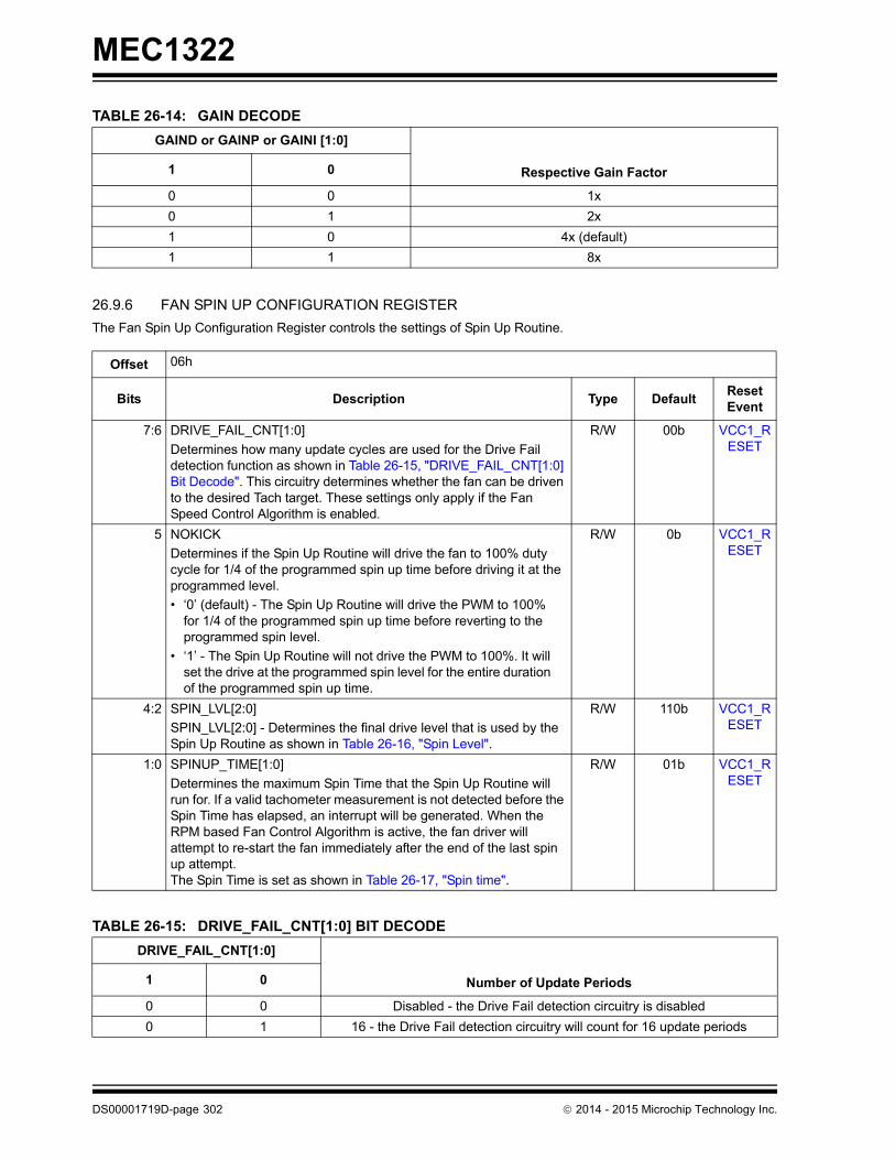
MEC1322
26.9.6 FAN SPIN UP CONFIGURATION REGISTER
The Fan Spin Up Configuration Register controls the settings of Spin Up Routine.
TABLE 26-14: GAIN DECODE
GAIND or GAINP or GAINI [1:0]
Respective Gain Factor1 0
0 0 1x
0 1 2x
1 0 4x (default)
1 1 8x
Offset 06h
Bits Description Type DefaultReset Event
7:6 DRIVE_FAIL_CNT[1:0]
Determines how many update cycles are used for the Drive Fail detection function as shown in Table 26-15, "DRIVE_FAIL_CNT[1:0] Bit Decode". This circuitry determines whether the fan can be driven to the desired Tach target. These settings only apply if the Fan Speed Control Algorithm is enabled.
R/W 00b VCC1_RESET
5 NOKICK
Determines if the Spin Up Routine will drive the fan to 100% duty cycle for 1/4 of the programmed spin up time before driving it at the programmed level.
• ‘0’ (default) - The Spin Up Routine will drive the PWM to 100% for 1/4 of the programmed spin up time before reverting to the programmed spin level.
• ‘1’ - The Spin Up Routine will not drive the PWM to 100%. It will set the drive at the programmed spin level for the entire duration of the programmed spin up time.
R/W 0b VCC1_RESET
4:2 SPIN_LVL[2:0]
SPIN_LVL[2:0] - Determines the final drive level that is used by the Spin Up Routine as shown in Table 26-16, "Spin Level".
R/W 110b VCC1_RESET
1:0 SPINUP_TIME[1:0]
Determines the maximum Spin Time that the Spin Up Routine will run for. If a valid tachometer measurement is not detected before the Spin Time has elapsed, an interrupt will be generated. When the RPM based Fan Control Algorithm is active, the fan driver will attempt to re-start the fan immediately after the end of the last spin up attempt.The Spin Time is set as shown in Table 26-17, "Spin time".
R/W 01b VCC1_RESET
TABLE 26-15: DRIVE_FAIL_CNT[1:0] BIT DECODE
DRIVE_FAIL_CNT[1:0]
Number of Update Periods1 0
0 0 Disabled - the Drive Fail detection circuitry is disabled
0 1 16 - the Drive Fail detection circuitry will count for 16 update periods
DS00001719D-page 302 2014 - 2015 Microchip Technology Inc.

MEC1322
26.9.7 FAN STEP REGISTER
The Fan Step Register, along with the Update Time, controls the ramp rate of the fan driver response calculated by theRPM based Fan Control Algorithm for the Derivative Options field values of “00” and “01” in the Fan Configuration 2Register (see Table 26-12, “Derivative Options,” on page 301).
The value of the register represents the maximum step size the fan driver will take for each update (see Section 26.9.3,"Fan Configuration 1 Register," on page 298).
When the maximum step size limitation is applied, if the necessary fan driver delta is larger than the Fan Step, it will becapped at the Fan Step setting and updated every Update Time ms.
The maximum step size is ignored for the Derivative Options field values of “10” and “11”.
1 0 32 - the Drive Fail detection circuitry will count for 32 update periods
1 1 64 - the Drive Fail detection circuitry will count for 64 update periods
TABLE 26-16: SPIN LEVEL
SPIN_LVL[2:0]
Spin Up Drive Level2 1 0
0 0 0 30%
0 0 1 35%
0 1 0 40%
0 1 1 45%
1 0 0 50%
1 0 1 55%
1 1 0 60% (default)
1 1 1 65%
TABLE 26-17: SPIN TIME
SPINUP_TIME[1:0]
Total Spin Up Time1 0
0 0 250 ms
0 1 500 ms (default)
1 0 1 sec
1 1 2 sec
Offset 07h
Bits Description Type DefaultReset Event
7:6 RESERVED R/W 00h -
5:0 FAN_STEP[5:0]
The Fan Step value represents the maximum step size the fan driverwill take between update times
R/W 10h VCC1_RESET
TABLE 26-15: DRIVE_FAIL_CNT[1:0] BIT DECODE (CONTINUED)
DRIVE_FAIL_CNT[1:0]
Number of Update Periods1 0
2014 - 2015 Microchip Technology Inc. DS00001719D-page 303

MEC1322
26.9.8 FAN MINIMUM DRIVE REGISTER
the Fan Minimum Drive Register stores the minimum drive setting for the RPM based Fan Control Algorithm. The RPMbased Fan Control Algorithm will not drive the fan at a level lower than the minimum drive unless the target Fan Speedis set at FFh (see "TACH Target Registers").
During normal operation, if the fan stops for any reason (including low drive), the RPM based Fan Control Algorithm willattempt to restart the fan. Setting the Fan Minimum Drive Registers to a setting that will maintain fan operation is a usefulway to avoid potential fan oscillations as the control circuitry attempts to drive it at a level that cannot support fan oper-ation.
These registers only apply if the Fan Speed Control Algorithm is used.
APPLICATION NOTE: To ensure proper operation, the Fan Minimum Drive register must be set prior to setting theTach Target High and Low Byte registers, and then the Tach Target registers can besubsequently updated. At a later time, if the Fan Minimum Drive register is changed to avalue higher than current Fan value, the Tach Target registers must also be updated.
26.9.9 VALID TACH COUNT REGISTER
The Valid TACH Count Register stores the maximum TACH Reading Register value to indicate that the fan is spinningproperly. The value is referenced at the end of the Spin Up Routine to determine if the fan has started operating anddecide if the device needs to retry. See the equation in the TACH Reading Registers section for translating the RPM toa count.
If the TACH Reading Register value exceeds the Valid TACH Count Register (indicating that the Fan RPM is below thethreshold set by this count), a stalled fan is detected. In this condition, the algorithm will automatically begin its Spin UpRoutine.
APPLICATION NOTE: The automatic invoking of the Spin Up Routine only applies if the Fan Speed ControlAlgorithm is used. If the FSC is disabled, then the device will only invoke the Spin Up Routinewhen the PWM setting changes from 00h.
If a TACH Target setting is set above the Valid TACH Count setting, that setting will be ignored and the algorithm willuse the current fan drive setting.
These registers only apply if the Fan Speed Control Algorithm is used.
26.9.10 FAN DRIVE FAIL BAND REGISTER
The Fan Drive Fail Band Registers store the number of Tach counts used by the Fan Drive Fail detection circuitry. Thiscircuitry is activated when the fan drive setting high byte is at FFh. When it is enabled, the actual measured fan speedis compared against the target fan speed.
This circuitry is used to indicate that the target fan speed at full drive is higher than the fan is actually capable of reaching.If the measured fan speed does not exceed the target fan speed minus the Fan Drive Fail Band Register settings for aperiod of time longer than set by the DRIVE_FAIL_CNTx[1:0] bits in the Fan Spin Up Configuration Register on page302, the DRIVE_FAIL status bit will be set and an interrupt generated.
These registers only apply if the Fan Speed Control Algorithm is used.
Offset 08h
Bits Description Type DefaultReset Event
7:0 MIN_DRIVE[7:0]
The minimum drive setting.
R/W 66h VCC1_RESET
Offset 09h
Bits Description Type DefaultReset Event
7:0 VALID_TACH_CNT[7:0]
The maximum TACH Reading Register value to indicate that the fan is spinning properly.
R/W F5h VCC1_RESET
DS00001719D-page 304 2014 - 2015 Microchip Technology Inc.

MEC1322
26.9.11 TACH TARGET REGISTER
The TACH Target Registers hold the target tachometer value that is maintained for the RPM based Fan Control Algo-rithm.
If the algorithm is enabled, setting the TACH Target Register High Byte to FFh will disable the fan driver (or set the PWMduty cycle to 0%). Setting the TACH Target to any other value (from a setting of FFh) will cause the algorithm to invokethe Spin Up Routine after which it will function normally.
These registers only apply if the Fan Speed Control Algorithm is used.
26.9.12 TACH READING REGISTER
The TACH Reading Registers’ contents describe the current tachometer reading for the fan. By default, the data rep-resents the fan speed as the number of 32.768kHz clock periods that occur for a single revolution of the fan.
The Equation below shows the detailed conversion from tachometer measurement (COUNT) to RPM.
where:
- Poles = number of poles of the fan (typically 2)
- fTACH = the frequency of the tachometer measurement clock
- n = number of edges measured (typically 5 for a 2 pole fan)
- m = the multiplier defined by the RANGE bits
- COUNT = TACH Reading Register value (in decimal)
The following equation shows the simplified translation of the TACH Reading Register count to RPM assuming a 2-polefan, measuring 5 edges, with a frequency of 32.768kHz.
Offset 0Ah
Bits Description Type DefaultReset Event
15:3 FAN_DRIVE_FAIL_BAND[12:0]
The number of Tach counts used by the Fan Drive Fail detection cir-cuitry
RES 0000000000000b
VCC1_RESET
2:0 RESERVED R/W 000b -
Offset 0Ch
Bits Description Type DefaultReset Event
15:3 TACH_TARGET[12:0]
The target tachometer value.
RES 1111111111111b
VCC1_RESET
2:0 RESERVED R/W 000b -
RPM1
Poles-------------- n 1–( )
COUNT1m----×
--------------------------------× fTACH× 60×=
RPM3932160 m×COUNT
-------------------------------=
2014 - 2015 Microchip Technology Inc. DS00001719D-page 305

MEC1322
26.9.13 PWM DRIVER BASE FREQUENCY REGISTER
- The PWM Driver Base Register controls the base PWM frequency range.
26.9.14 FAN STATUS REGISTER
The bits in this register are routed to interrupts.
Offset 0Eh
Bits Description Type DefaultReset Event
15:3 TACH_READING[12:0]
The current tachometer reading value.
RES 1111111111111b
VCC1_RESET
2:0 RESERVED R/W 000b -
Offset 10h
Bits Description Type DefaultReset Event
7:2 RESERVED RES 000000b -
1:0 PWM_BASE[1:0]
Determines the frequency range of the PWM fan driver (when enabled) as shown in Table 26-18.
R/W 00b VCC1_RESET
TABLE 26-18: PWM_BASE[1:0] DECODE
PWM_BASE[1:0]
PWM Frequency1 0
0 0 26.83KHz
0 1 20.87kHz
1 0 4.82kHz
1 1 2.41KHz
Offset 11h
Bits Description Type DefaultReset Event
7:6 RESERVED RES 00b -
5 DRIVE_FAILThe bit Indicates that the RPM-based Fan Speed Control Algorithm cannot drive the Fan to the desired target setting at maximum drive.
• ‘0’ - The RPM-based Fan Speed Control Algorithm can drive Fan to the desired target setting.
• ‘1’ - The RPM-based Fan Speed Control Algorithm cannot drive Fan to the desired target setting at maximum drive.
R/WC 0b VCC1_RESET
4:2 RESERVED RES 000b -
DS00001719D-page 306 2014 - 2015 Microchip Technology Inc.

MEC1322
1 FAN_SPINThe bit Indicates that the Spin up Routine for the Fan could not detect a valid tachometer reading within its maximum time window.
• ‘0’ - The Spin up Routine for the Fan detected a valid tachome-ter reading within its maximum time window.
• ‘1’ - The Spin up Routine for the Fan could not detect a valid tachometer reading within its maximum time window.
R/WC 0b VCC1_RESET
0 FAN_STALLThe bit Indicates that the tachometer measurement on the Fan detects a stalled fan.
• ‘0’ - Stalled fan not detected.
• ‘1’ - Stalled fan not detected.
R/WC 0b VCC1_RESET
Offset 11h
Bits Description Type DefaultReset Event
2014 - 2015 Microchip Technology Inc. DS00001719D-page 307

MEC1322
27.0 GENERAL PURPOSE SERIAL PERIPHERAL INTERFACE
27.1 Overview
The General Purpose Serial Peripheral Interface (GP-SPI) may be used to communicate with various peripheraldevices, e.g., EEPROMS, DACs, ADCs, that use a standard Serial Peripheral Interface.
Characteristics of the GP-SPI Controller include:
• 8-bit serial data transmitted and received simultaneously over two data pins in Full Duplex mode with options to transmit and receive data serially on one data pin in Half Duplex (Bidirectional) mode.
• An internal programmable clock generator and clock polarity and phase controls allowing communication with var-ious SPI peripherals with specific clocking requirements.
• SPI cycle completion that can be determined by status polling or interrupts.
• The ability to read data in on both SPDIN and SPDOUT in parallel. This allows this SPI Interface to support dual data rate read accesses for emerging double rate SPI flashes
• Support of back-to-back reads and writes without clock stretching, provided the host can read and write the data registers within one byte transaction time.
27.2 References
No references have been cited for this feature.
27.3 Terminology
No terminology for this block.
27.4 Interface
This block is designed to be accessed externally via the pin interface and internally via a registered host interface.
FIGURE 27-1: I/O DIAGRAM OF BLOCK
General Purpose Serial Peripheral Interface
Interrupts
Power, Clocks and Reset
Host Interface Signal Description
DS00001719D-page 308 2014 - 2015 Microchip Technology Inc.

MEC1322
27.5 Signal Description
27.6 Host Interface
The registers defined for the General Purpose Serial Peripheral Interface are accessible by the various hosts as indi-cated in Section 27.12, "EC-Only Registers".
27.7 Power, Clocks and Reset
This section defines the Power, Clock, and Reset parameters of the block.
27.7.1 POWER DOMAINS
27.7.2 CLOCK INPUTS
27.7.3 RESETS
TABLE 27-1: SIGNAL DESCRIPTION TABLE
Name Direction Description
SPDIN Input Serial Data In pin
SPDOUT Input/Output Serial Data Output pin. Switches to input when used in double-data-rate mode
SPI_CLK Output SPI Clock output used to drive the SPCLK pin.
SPI_CS# Output SPI chip select
Note: The SPI block signals that are shown in Table 27-1 are routed to the SPI pins as listed in Table 27-2.
TABLE 27-2: SIGNAL TO PIN NAME LOOKUP TABLE
Block Name Pin Name
SPDIN SHD_MISO, PVT_MISO
SPDOUT SHD_MOSI, PVT_MOSI
SPI_CLK SHD_SCLK, PVT_SCLK
SPI_CS# SHD_CS0#, PVT_CS0#
TABLE 27-3: POWER SOURCES
Name Description
VCC1 The logic and registers implemented in this block are powered by this power well.
TABLE 27-4: CLOCK INPUTS
Name Description
48 MHz Ring Oscillator This is a clock source for the SPI clock generator.
2MHz This is a clock source for the SPI clock generator.
TABLE 27-5: RESET SIGNALS
Name Description
VCC1_RESET This signal resets all the registers and logic in this block to their default state.
2014 - 2015 Microchip Technology Inc. DS00001719D-page 309

MEC1322
27.8 Interrupts
This section defines the Interrupt Sources generated from this block.
These status bits are also connected respectively to the DMA Controller’s SPI Controller TX and RX requests signals.
27.9 Low Power Modes
The GP-SPI Interface may be put into a low power state by the chip’s Power, Clocks, and Reset (PCR) circuitry.
27.10 Description
The Serial Peripheral Interface (SPI) block is a master SPI block used to communicate with external SPI devices. TheSPI master is responsible for generating the SPI clock and is designed to operate in Full Duplex, Half Duplex, and Dualmodes of operation. The clock source may be programmed to operated at various clock speeds. The data is transmit-ted serially via 8-bit transmit and receive shift registers. Communication with SPI peripherals that require transactionsof varying lengths can be achieved with multiple 8-bit cycles.
This block has many configuration options: The data may be transmitted and received either MSbit or LSbit first; TheSPI Clock Polarity may be either active high or active low; Data may be sampled or presented on either the rising offalling edge of the clock (referred to as the transmit clock phase); and the SPI_CLK SPDOUT frequency may be pro-grammed to a range of values as illustrated in Table 27-7, "SPI_CLK Frequencies". In addition to these many program-mable options, this feature has several status bits that may be enabled to notify the host that data is being transmittedor received.
27.10.1 INITIATING AN SPI TRANSACTION
All SPI transactions are initiated by a write to the TX_DATA register. No read or write operations can be initiated untilthe Transmit Buffer is Empty, which is indicated by a one in the TXBE status bit.
If the transaction is a write operation, the host writes the TX_DATA register with the value to be transmitted. Writing theTX_DATA register causes the TXBE status bit to be cleared, indicating that the value has been registered. If empty, theSPI Core loads this TX_DATA value into an 8-bit transmit shift register and begins shifting the data out. Loading thevalue into the shift register causes the TXBE status bit to be asserted, indicating to software that the next byte can bewritten to the TX_DATA register.
If the transaction is a read operation, the host initiates a write to the TX_DATA register in the same manner as the writeoperation. Unlike the transmit command, the host must clear the RXBF status bit by reading the RX_DATA registerbefore writing the TX_DATA register. This time, the host will be required to poll the RXBF status bit to determine whenthe value in the RX_DATA register is valid.
Note 1: If the SPI interface is configured for Half Duplex mode, the host must still write a dummy byte to receive data.
2: Since RX and TX transactions are executed by the same sequence of transactions, data is always shiftedinto the RX_DATA register. Therefore, every write operation causes data to be latched into the RX_DATAregister and the RXBF bit is set. This status bit should be cleared before initiating subsequent transactions.The host utilizing this SPI core to transmit SPI Data must discard the unwanted receive bytes.
3: The length and order of data sent to and received from a SPI peripheral varies between peripheral devices.The SPI must be properly configured and software-controlled to communicate with each device and deter-mine whether SPIRD data is valid slave data.
The following diagrams show sample single byte and multi-byte SPI Transactions.
TABLE 27-6: EC INTERRUPTS
Source Description
TXBE_STS Transmit buffer empty status (TXBE), in the SPI Status Register, sent as an interrupt request to the Interrupt Aggregator.
RXBF_STS Receive buffer full status (RXBF), in the SPI Status Register, sent as an interrupt request to the Interrupt Aggregator.
DS00001719D-page 310 2014 - 2015 Microchip Technology Inc.

MEC1322
FIGURE 27-2: SINGLE BYTE SPI TX/RX TRANSACTIONS (FULL DUPLEX MODE)
Single SPI BYTE Transactions
Rx_DATA Buffer Full (RxBF)
TX_DATA Buffer Empty (TxBE)
Write TX_Data
MCLK
SPDOUT_Direction
TX_DATA BYTE 0
Read RX_Data
RX_DATA BYTE 0
Data Out Shift Register 7 6 5 4 3 2 1 0
Data In Shift Register 7 6 5 4 3 2 1 0
SPCLKO
2014 - 2015 Microchip Technology Inc. DS00001719D-page 311

MEC1322
The data may be configured to be transmitted MSB or LSB first. This is configured by the LSBF bit in the SPI ControlRegister. The transmit data is shifted out on the edge as selected by the TCLKPH bit in the SPI Clock Control Register.All received data can be sampled on a rising or falling SPI_CLK edge using the RCLKPH bit in the SPI Clock ControlRegister This clock setting must be identical to the clocking requirements of the current SPI slave.
There are three types of transactions that can be implemented for transmitting and receiving the SPI data. They are FullDuplex, Half Duplex, and Dual Mode. These modes are define in Section 27.10.3, "Types of SPI Transactions".
27.10.2 DMA MODE
Transmit and receive operations can use a DMA channel. Note that only one DMA channel may be enabled at atime. Setting up the DMA Controller involves specifying the device (Flash GP-SPI), direction (transmit/receive), andthe start and end addresses of the DMA buffers in the closely couple memory. Please refer to the DMA Controller chap-ter for register programming information.
SPI transmit / DMA write: the GP-SPI block’s transmit empty (TxBE) status signal is used as a write request to the DMAcontroller, which then fetches a byte from the DMA transmit buffer and writes it to the GP-SPI’s SPI TX Data Register(SPITD). As content of the latter is transferred to the internal Tx shift register from which data is shifted out onto the SPIbus bit by bit, the Tx Empty signal is again asserted, triggering the DMA fetch-and-write cycle. The process continuesuntil the end of the DMA buffer is reached - the DMA controller stops responding to an active Tx Empty until the buffer’saddress registers are reprogrammed.
SPI receive / DMA read: the AUTO_READ bit in the SPI Control Register must be set. The driver first writes (dummydata) to the SPI TX Data Register (SPITD) to initiate the toggling of the SPI clock, enabling data to be shifted in. Afterone byte is received, the Rx Full (RxBF) status signal, used as a read request to the DMA controller, is asserted. The
FIGURE 27-3: MULTI-BYTE SPI TX/RX TRANSACTIONS (FULL DUPLEX MODE)
Note: Common peripheral devices require a chip select signal to be asserted during a transaction. Chip selectsfor SPI devices may be controlled by MEC1322 GPIO pins.
SPI BYTE Transactions
Rx_DATA Buffer Full (RxBF)
TX_DATA Buffer Empty (TxBE)
Write TX_Data
MCLK
SPDOUT_Direction
TX_DATABYTE
0 BYTE 1 BYTE 2
Read RX_Data
RX_DATA BYTE 0 BYTE 1 BYT
Data Out Shift Register 7 6 5 4 3 2 1 0 7 6 5 4 3 2 1 0
Data In Shift Register 7 6 5 4 3 2 1 0 7 6 5 4 3 2 1 0
SPCLKO
7 6 5 4 3 2
7 6 5 4 3 2
1 0
1 0
DS00001719D-page 312 2014 - 2015 Microchip Technology Inc.

MEC1322
DMA controller then reads the received byte from the GP-SPI’s SPI RX Data Register (SPIRD) and stores it in the DMAreceive buffer. With AUTO_READ set, this read clears both the RxBF and TxBE. Clearing TxBE causes (dummy) datafrom the SPI TX Data Register (SPITD) to be transferred to the internal shift register, mimicking the effect of the afore-mentioned write to the SPI TX Data Register (SPITD) by the driver. SPI clock is toggled again to shift in the second readbyte. This process continues until the end of the DMA buffer is reached - the DMA controller stops responding to anactive Tx Empty until the buffer’s address registers are reprogrammed.
27.10.3 TYPES OF SPI TRANSACTIONS
The GP-SPI controller can be configured to operate in three modes: Full Duplex, Half Duplex, and Dual Mode.
27.10.3.1 Full Duplex
In Full Duplex Mode, serial data is transmitted and received simultaneously by the SPI master over the SPDOUT andSPDIN pins. To enable Full Duplex Mode clear SPDIN Select.
When a transaction is completed in the full-duplex mode, the RX_DATA shift register always contains received data(valid or not) from the last transaction.
27.10.3.2 Half Duplex
In Half Duplex Mode, serial data is transmitted and received sequentially over a single data line (referred to as the SPD-OUT pin). To enable Half Duplex Mode set SPDIN Select to 01b. The direction of the SPDOUT signal is determined bythe BIOEN bit.
• To transmit data in half duplex mode set the BIOEN bit before writing the TX_DATA register.
• To receive data in half duplex mode clear the BIOEN bit before writing the TX_DATA register with a dummy byte.
27.10.3.3 Dual Mode of Operation
In Dual Mode, serial data is transmitted sequentially from the SPDOUT pin and received in by the SPI master from theSPDOUT and SPDIN pins. This essentially doubles the received data rate and is often available in SPI Flash devices.To enable Dual Mode of operation the SPI core must be configured to receive data in path on the SPDIN1 and SPDIN2inputs via SPDIN Select. The BIOEN bit determines if the SPI core is transmitting or receiving. The setting of this bitdetermines the direction of the SPDOUT signal. The SPDIN Select bits are configuration bits that remain static for theduration of a dual read command. The BIOEN bit must be toggled to indicate when the SPI core is transmitting andreceiving.
• To transmit data in dual mode set the BIOEN bit before writing the TX_DATA register.
• To receive data in dual mode clear the BIOEN bit before writing the TX_DATA register with a dummy byte. The even bits (0,2,4,and 6) are received on the SPDOUT pin and the odd bits (1,3,5,and 7) are received on the SPDIN pin. The hardware assembles these received bits into a single byte and loads them into the RX_DATA register accordingly.
The following diagram illustrates a Dual Fast Read Command that is supported by some SPI Flash devices.
Note: The Software driver must properly drive the BIOEN bit and store received data depending on the transac-tion format of the specific slave device.
2014 - 2015 Microchip Technology Inc. DS00001719D-page 313
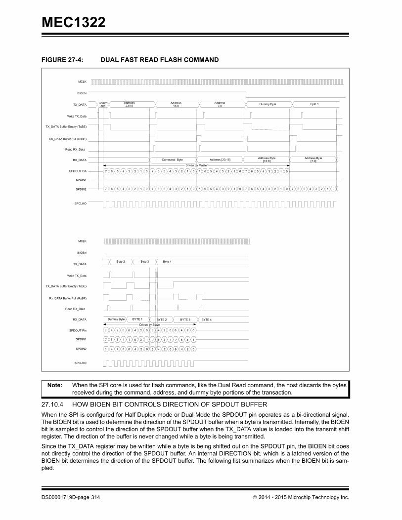
MEC1322
27.10.4 HOW BIOEN BIT CONTROLS DIRECTION OF SPDOUT BUFFER
When the SPI is configured for Half Duplex mode or Dual Mode the SPDOUT pin operates as a bi-directional signal.The BIOEN bit is used to determine the direction of the SPDOUT buffer when a byte is transmitted. Internally, the BIOENbit is sampled to control the direction of the SPDOUT buffer when the TX_DATA value is loaded into the transmit shiftregister. The direction of the buffer is never changed while a byte is being transmitted.
Since the TX_DATA register may be written while a byte is being shifted out on the SPDOUT pin, the BIOEN bit doesnot directly control the direction of the SPDOUT buffer. An internal DIRECTION bit, which is a latched version of theBIOEN bit determines the direction of the SPDOUT buffer. The following list summarizes when the BIOEN bit is sam-pled.
FIGURE 27-4: DUAL FAST READ FLASH COMMAND
Note: When the SPI core is used for flash commands, like the Dual Read command, the host discards the bytesreceived during the command, address, and dummy byte portions of the transaction.
Rx_DATA Buffer Full (RxBF)
TX_DATA Buffer Empty (TxBE)
Write TX_Data
MCLK
BIOEN
TX_DATA
Read RX_Data
RX_DATA Dummy Byte BYTE 1
SPDOUT Pin
SPDIN1
SPCLKO
SPDIN2
Rx_DATA Buffer Full (RxBF)
TX_DATA Buffer Empty (TxBE)
Write TX_Data
Read RX_Data
RX_DATA
SPCLKO
SPDOUT Pin 7 6
SPDIN1
7 6SPDIN2
Command Byte Address [23:16]Address Byte
[16:8]
5 4 3 2 1 0 7 6 5 4 3 2 1 0
5 4 3 2 1 0 7 6 5 4 3 2 1 0
7 6 5 4 3 2
7 6 5 4 3 2
1 0
1 0
7 6 5 4 3 2
7 6 5 4 3 2
1 0
1 0 7 6 5 4 3 2 1 0
Address Byte [7:0]
BIOEN
TX_DATAComm
andAddress
23:16Address
15:8Address
7:0
MCLK
Dummy Byte Byte 1
Byte 2 Byte 3 Byte 4
5 3 1
6 4 2 0
7 5 3 1
6 4 2 0
7 5 3 1
6 4 2 0
7 5 3 1
6 4 2 0
7
BYTE 2 BYTE 3 BYTE 4
6 4 2 0 6 4 2 0 6 4 2 0 6 4 2 0
Driven by Master
Driven by Slave
DS00001719D-page 314 2014 - 2015 Microchip Technology Inc.

MEC1322
• The DIRECTION bit is equal to the BIOEN bit when data is not being shifted out (i.e., SPI interface is idle).
• The hardware samples the BIOEN bit when it is shifting out the last bit of a byte to determine if the buffer needs to be turned around for the next byte.
• The BIOEN bit is also sampled any time the value in the TX_DATA register is loaded into the shift register to be transmitted.
If a TAR (Turn-around time) is required between transmitting and receiving bytes on the SPDOUT signal, softwareshould allow all the bytes to be transmitted before changing the buffer to an input and then load the TX_DATA registerto begin receiving bytes. If TAR greater than zero is required, software must wait for the transmission in one directionto complete before writing the TX_DATA register to start sending/receiving in the opposite direction. This allows the SPIblock to operate the same as legacy Microchip SPI devices.
27.10.5 CONFIGURING THE SPI CLOCK GENERATOR
The SPI controller generates the SPI_CLK signal to the external SPI device. The frequency of the SPI_CLK signal isdetermined by one of two clock sources and the Preload value of the clock generator down counter. The clock generatortoggles the SPI_CLK output every time the counter underflows, while data is being transmitted.
The clock source to the down counter is determined by Bit CLKSRC. Either the main system clock or the 2MHz clockcan be used to decrement the down counter in the clock generator logic.
The SPI_CLK frequency is determined by the following formula:
The REFERENCE_CLOCK frequency is selected by CLKSRC in the SPI Clock Control Register and PRELOAD is thePRELOAD field of the SPI Clock Generator Register. The frequency can be either the 48 MHz Ring Oscillator clock ora 2MHz clock. When the PRELOAD value is 0, the REFERENCE_CLOCK is always the 48 MHz Ring Oscillator clockand the CLKSRC bit is ignored.
Sample SPI Clock frequencies are shown in the following table:
27.10.6 CONFIGURING SPI MODE
In practice, there are four modes of operation that define when data should be latched. These four modes are the com-binations of the SPI_CLK polarity and phase.
The output of the clock generator may be inverted to create an active high or active low clock pulse. This is used todetermine the inactive state of the SPI_CLK signal and is used for determining the first edge for shifting the data. Thepolarity is selected by CLKPOL in the SPI Clock Control Register.
Note: When the SPI interface is in the idle state and data is not being transmitted, the SPI_CLK signal stops inthe inactive state as determined by the configuration bits.
TABLE 27-7: SPI_CLK FREQUENCIES
Clock Source PRELOAD SPI_CLK Frequency
Don’t Care 0 48MHz
48MHz 1 24MHz
48MHz 2 12MHz(default)
48MHz 3 6MHz
48MHz 63 381KHz
2MHz 1 1MHz
2MHz 2 500KHz
2MHz 3 333KHz
2MHz 63 15.9KHz
SPI_CLK_FREQ=12--- REFERENCE_CLOCK× PRELOAD⁄
2014 - 2015 Microchip Technology Inc. DS00001719D-page 315

MEC1322
The phase of the clock is selected independently for receiving data and transmitting data. The receive phase is deter-mine by RCLKPH and the transmit phase is determine by TCLKPH in the SPI Clock Control Register.
The following table summarizes the effect of CLKPOL, RCLKPH and TCLKPH.
27.11 SPI Examples
27.11.1 FULL DUPLEX MODE TRANSFER EXAMPLES
27.11.1.1 Read Only
The slave device used in this example is a MAXIM MAX1080 10 bit, 8 channel ADC:
• The SPI block is activated by setting the enable bit in SPIAR - SPI Enable Register
• The SPIMODE bit is de-asserted '0' to enable the SPI interface in Full Duplex mode.
• The CLKPOL and TCLKPH bits are de-asserted '0', and RCLKPH is asserted '1' to match the clocking require-ments of the slave device.
• The LSBF bit is de-asserted '0' to indicate that the slave expects data in MSB-first order.
• Assert CS# using a GPIO pin.
• Write a valid command word (as specified by the slave device) to the SPITD - SPI TX_Data Register with TXFE asserted '1'. The SPI master automatically clears the TXFE bit indicating the byte has been put in the TX buffer. If the shift register is empty the TX_DATA byte is loaded into the shift register and the SPI master reasserts the TXFE bit. Once the data is in the shift register the SPI master begins shifting the data value onto the SPDOUT pin and drives the SPCLK pin. Data on the SPDIN pin is also sampled on each clock.
• Once the TXFE bit is asserted the SPI Master is ready to receive its next byte. Before writing the next TX_DATA value, software must clear the RXBF status bit by reading the SPIRD - SPI RX_Data Register.
TABLE 27-8: SPI DATA AND CLOCK BEHAVIOR
CLKPOL RCLKPH TCLKPH Behavior
0 0 0 Inactive state is low. First edge is rising edge.Data is sampled on the rising edge.Data is transmitted on the falling edge. Data is valid before the first rising edge.
0 0 1 Inactive state is low. First edge is rising edge.Data is sampled on the rising edge.Data is transmitted on the rising edge.
0 1 0 Inactive state is low. First edge is rising edge.Data is sampled on the falling edge.Data is transmitted on the falling edge. Data is valid before the first rising edge.
0 1 1 Inactive state is low. First edge is rising edge.Data is sampled on the falling edge.Data is transmitted on the rising edge.
1 0 0 Inactive state is high. First edge is falling edge.Data is sampled on the falling edge.Data is transmitted on the rising edge. Data is valid before the first falling edge.
1 0 1 Inactive state is high. First edge is falling edge.Data is sampled on the falling edge.Data is transmitted on the falling edge.
1 1 0 Inactive state is high. First edge is falling edge.Data is sampled on the rising edge.Data is transmitted on the rising edge. Data is valid before the first falling edge.
1 1 1 Inactive state is high. First edge is falling edge.Data is sampled on the rising edge.Data is transmitted on the falling edge.
DS00001719D-page 316 2014 - 2015 Microchip Technology Inc.

MEC1322
• A dummy 8 bit data value (any value) is written to the TX_DATA register. The SPI master automatically clears the TXFE bit, but does not begin shifting the dummy data value onto the SPDOUT pin. This byte will remain in the TX_DATA register until the TX shift register is empty.
• After 8 SPI_CLK pulses from the first transmit bytes:
- The first SPI cycle is complete, RXBF bit is asserted '1', and the SPINT interrupt is asserted, if enabled. The data now contained in SPIRD - SPI RX_Data Register is invalid since the last cycle was initiated solely to transmit command data to the slave. This particular slave device drives '0' on the SPDIN pin to the master while it is accepting command data. This SPIRD data is ignored.
- Once the first SPI cycle is completed, the SPI master takes the pending data in the TX_DATA register and loads it into the TX shift register. Loading the shift register automatically asserts the TXFE bit, begins shifting the dummy data value onto the SPDOUT pin, and drives the SPCLK pin. Data on the SPDIN pin is also sam-pled on each clock.
• Once the TXFE bit is asserted the SPI Master is ready to receive its next byte. Before writing the next TX_DATA value, software must clear the RXBF status bit by reading the SPIRD - SPI RX_Data Register.
• The final SPI cycle is initiated when another dummy 8 bit data value (any value) is written to the TX_DATA regis-ter. Note that this value may be another dummy value or it can be a new 8 bit command to be sent to the ADC. The new command will be transmitted while the final data from the last command is received simultaneously. This overlap allows ADC data to be read every 16 SPCLK cycles after the initial 24 clock cycle.The SPI master auto-matically clears the TXFE bit, but does not begin shifting the dummy data value onto the SPDOUT pin. This byte will remain in the TX_DATA register until the TX shift register is empty.
• After 8 SPI_CLK pulses, the second SPI cycle is complete:
- The first SPI cycle is complete, RXBF bit is asserted '1', and the SPINT interrupt is asserted, if enabled. The data now contained in SPIRD - SPI RX_Data Register is the first half of a valid 16 bit ADC value. SPIRD is read and stored.
- Once the second SPI cycle is completed, the SPI master takes the pending data in the TX_DATA register and loads it into the TX shift register. Loading the shift register automatically asserts the TXFE bit, begins shifting the data value onto the SPDOUT pin, and drives the SPCLK pin. Data on the SPDIN pin is also sampled on each clock.
• After 8 SPI_CLK pulses, the final SPI cycle is complete, TXBF is asserted '1', and the SPINT interrupt is asserted (if enabled). The data now contained in SPIRD - SPI RX_Data Register is the second half of a valid 16 bit ADC value. SPIRD is read and stored.
• If a command was overlapped with the received data in the final cycle, #CS should remain asserted and the SPI master will initiate another SPI cycle. If no new command was sent, #CS is released and the SPI is idle.
27.11.1.2 Read/Write
The slave device used in this example is a Fairchild NS25C640 FM25C640 64K Bit Serial EEPROM. The following sub-sections describe the read and write sequences.
Read
• The SPI block is activated by setting the enable bit in SPIAR - SPI Enable Register
• The SPIMODE bit is de-asserted '0' to enable the SPI interface in Full Duplex mode.
• The CLKPOL, TCLKPH and RCLKPH bits are de-asserted '0' to match the clocking requirements of the slave device.
• The LSBF bit is de-asserted '0' to indicate that the slave expects data in MSB-first order.
• Assert CS# low using a GPIO pin.
• Write a valid command word (as specified by the slave device) to the SPITD - SPI TX_Data Register with TXFE asserted '1'. The SPI master automatically clears the TXFE bit indicating the byte has been put in the TX buffer. If the shift register is empty the TX_DATA byte is loaded into the shift register and the SPI master reasserts the TXFE bit. Once the data is in the shift register the SPI master begins shifting the data value onto the SPDOUT pin and drives the SPI_CLK pin. Data on the SPDIN pin is also sampled on each clock.
• Once the TXFE bit is asserted the SPI Master is ready to receive its next byte. Before writing the next TX_DATA value, software must clear the RXBF status bit by reading the SPIRD - SPI RX_Data Register.
• Next, EEPROM address A15-A8 is written to the TX_DATA register. The SPI master automatically clears the TXFE bit, but does not begin shifting the dummy data value onto the SPDOUT pin. This byte will remain in the TX_DATA register until the TX shift register is empty.
2014 - 2015 Microchip Technology Inc. DS00001719D-page 317

MEC1322
• After 8 SPI_CLK pulses from the first transmit byte (Command Byte transmitted):
- The first SPI cycle is complete, RXBF bit is asserted '1', and the SPINT interrupt is asserted, if enabled. The data now contained in SPIRD - SPI RX_Data Register is invalid since the last cycle was initiated solely to transmit command data to the slave. This particular slave device tri-states the SPDIN pin to the master while it is accepting command data. This SPIRD data is ignored.
- Once the first SPI cycle is completed, the SPI master takes the pending data in the TX_DATA register (EEPROM address A15-A8) and loads it into the TX shift register. Loading the shift register automatically asserts the TXFE bit, begins shifting the dummy data value onto the SPDOUT pin, and drives the SPI_CLK pin. Data on the SPDIN pin is also sampled on each clock. Note: The particular slave device ignores address A15-A13.
• Once the TXFE bit is asserted the SPI Master is ready to receive its next byte. Before writing the next TX_DATA value, software must clear the RXBF status bit by reading the SPIRD - SPI RX_Data Register.
• Next, EEPROM address A7-A0 is written to the TX_DATA register. The SPI master automatically clears the TXFE bit, but does not begin shifting this data value onto the SPDOUT pin. This byte will remain in the TX_DATA register until the TX shift register is empty.
• After 8 SPI_CLK pulses from the second transmit byte (Address Byte (MSB) transmitted):
- EEPROM address A15-A8 has been transmitted to the slave completing the second SPI cycle. Once again, the RXBF bit is asserted '1' and the SPINT interrupt is asserted, if enabled. The data now contained in SPIRD - SPI RX_Data Register is invalid since the last cycle was initiated solely to transmit address data to the slave.
- Once the second SPI cycle is completed, the SPI master takes the pending data in the TX_DATA register (EEPROM address A7-A0) and loads it into the TX shift register. Loading the shift register automatically asserts the TXFE bit, begins shifting the dummy data value onto the SPDOUT pin, and drives the SPCLK pin. Data on the SPDIN pin is also sampled on each clock.
• Once the TXFE bit is asserted the SPI Master is ready to receive its next byte. Before writing the next TX_DATA value, software must clear the RXBF status bit by reading the SPIRD - SPI RX_Data Register.
• Next, a dummy byte is written to the TX_DATA register. The SPI master automatically clears the TXFE bit, but does not begin shifting this data value onto the SPDOUT pin. This byte will remain in the TX_DATA register until the TX shift register is empty.
• After 8 SPI_CLK pulses, the third SPI cycle is complete (Address Byte (LSB) transmitted):
- EEPROM address A7-A0 has been transmitted to the slave completing the third SPI cycle. Once again, the RXBF bit is asserted '1' and the SPINT interrupt is asserted, if enabled. The data now contained in SPIRD - SPI RX_Data Register is invalid since the last cycle was initiated solely to transmit address data to the slave.
- Once the third SPI cycle is completed, the SPI master takes the pending data in the TX_DATA register (dummy byte) and loads it into the TX shift register. Loading the shift register automatically asserts the TXFE bit, begins shifting the dummy data value onto the SPDOUT pin, and drives the SPCLK pin. Data on the SPDIN pin is also sampled on each clock.
• Once the TXFE bit is asserted the SPI Master is ready to receive its next byte. Before writing the next TX_DATA value, software must clear the RXBF status bit by reading the SPIRD - SPI RX_Data Register.
• If only one receive byte is required, the host would not write any more value to the TX_DATA register until this transaction completes. If more than one byte of data is to be received, another dummy byte would be written to the TX_DATA register (one dummy byte per receive byte is required). The SPI master automatically clears the TXFE bit when the TX_DATA register is written, but does not begin shifting this data value onto the SPDOUT pin. This byte will remain in the TX_DATA register until the TX shift register is empty.
• After 8 SPI_CLK pulses, the fourth SPI cycle is complete (First Data Byte received):
- The dummy byte has been transmitted to the slave completing the fourth SPI cycle. Once again, the RXBF bit is asserted '1' and the SPINT interrupt is asserted, if enabled. Unlike the command and address phases, the data now contained in SPIRD - SPI RX_Data Register is the 8-bit EEPROM data since the last cycle was ini-tiated to receive data from the slave.
- Once the fourth SPI cycle is completed, the SPI master takes the pending data in the TX_DATA register (if any) and loads it into the TX shift register. This process will be repeated until all the desired data is received.
• The host software will read and store the EEPROM data value in SPIRD - SPI RX_Data Register.
Note: External pull-up or pull-down is required on the SPDIN pin if it is tri-stated by the slave device.
DS00001719D-page 318 2014 - 2015 Microchip Technology Inc.
MEC1322
• If no more data needs to be received by the master, CS# is released and the SPI is idle. Otherwise, master contin-ues reading the data by writing a dummy value to the TX_DATA register after every 8 SPI_CLK cycles.
Write
• The SPI block is activated by setting the enable bit in SPIAR - SPI Enable Register
• The SPIMODE bit is de-asserted '0' to enable the SPI interface in Full Duplex mode.
• The CLKPOL, TCLKPH and RCLKPH bits are de-asserted '0' to match the clocking requirements of the slave device.
• The LSBF bit is de-asserted '0' to indicate that the slave expects data in MSB-first order.
• Assert WR# high using a GPIO pin.
• Assert CS# low using a GPIO pin.
• Write a valid command word (as specified by the slave device) to the SPITD - SPI TX_Data Register with TXFE asserted '1'. The SPI master automatically clears the TXFE bit indicating the byte has been put in the TX buffer. If the shift register is empty the TX_DATA byte is loaded into the shift register and the SPI master reasserts the TXFE bit. Once the data is in the shift register the SPI master begins shifting the data value onto the SPDOUT pin and drives the SPI_CLK pin. Data on the SPDIN pin is also sampled on each clock.
• Once the TXFE bit is asserted the SPI Master is ready to receive its next byte. Before writing the next TX_DATA value, software must clear the RXBF status bit by reading the SPIRD - SPI RX_Data Register.
• Next, EEPROM address A15-A8 is written to the TX_DATA register. The SPI master automatically clears the TXFE bit, but does not begin shifting the dummy data value onto the SPDOUT pin. This byte will remain in the TX_DATA register until the TX shift register is empty.
• After 8 SPI_CLK pulses from the first transmit byte (Command Byte transmitted):
- The first SPI cycle is complete, RXBF bit is asserted '1', and the SPINT interrupt is asserted, if enabled. The data now contained in SPIRD - SPI RX_Data Register is invalid since the last cycle was initiated solely to transmit command data to the slave. This particular slave device tri-states the SPDIN pin to the master while it is accepting command data. This SPIRD data is ignored.
USER’S NOTE: External pull-up or pull-down is required on the SPDIN pin if it is tri-stated by the slave device.
- Once the first SPI cycle is completed, the SPI master takes the pending data in the TX_DATA register (EEPROM address A15-A8) and loads it into the TX shift register. Loading the shift register automatically asserts the TXFE bit, begins shifting the dummy data value onto the SPDOUT pin, and drives the SPI_CLK pin. Data on the SPDIN pin is also sampled on each clock. Note: The particular slave device ignores address A15-A13.
• Once the TXFE bit is asserted the SPI Master is ready to receive its next byte. Before writing the next TX_DATA value, software must clear the RXBF status bit by reading the SPIRD - SPI RX_Data Register.
• Next, EEPROM address A7-A0 is written to the TX_DATA register. The SPI master automatically clears the TXFE bit, but does not begin shifting this data value onto the SPDOUT pin. This byte will remain in the TX_DATA register until the TX shift register is empty.
• After 8 SPI_CLK pulses from the second transmit byte (Address Byte (MSB) transmitted):
- EEPROM address A15-A8 has been transmitted to the slave completing the second SPI cycle. Once again, the RXBF bit is asserted '1' and the SPINT interrupt is asserted, if enabled. The data now contained in SPIRD - SPI RX_Data Register is invalid since the last cycle was initiated solely to transmit address data to the slave.
- Once the second SPI cycle is completed, the SPI master takes the pending data in the TX_DATA register (EEPROM address A7-A0) and loads it into the TX shift register. Loading the shift register automatically asserts the TXFE bit, begins shifting the dummy data value onto the SPDOUT pin, and drives the SPCLK pin. Data on the SPDIN pin is also sampled on each clock.
• Once the TXFE bit is asserted the SPI Master is ready to receive its next byte. Before writing the next TX_DATA value, software must clear the RXBF status bit by reading the SPIRD - SPI RX_Data Register.
• Next, a data byte (D7:D0) is written to the TX_DATA register. The SPI master automatically clears the TXFE bit, but does not begin shifting this data value onto the SPDOUT pin. This byte will remain in the TX_DATA register until the TX shift register is empty.
• After 8 SPI_CLK pulses, the third SPI cycle is complete (Address Byte (LSB) transmitted):
- EEPROM address A7-A0 has been transmitted to the slave completing the third SPI cycle. Once again, the RXBF bit is asserted '1' and the SPINT interrupt is asserted, if enabled. The data now contained in SPIRD -
2014 - 2015 Microchip Technology Inc. DS00001719D-page 319

MEC1322
SPI RX_Data Register is invalid since the last cycle was initiated solely to transmit address data to the slave.
- Once the third SPI cycle is completed, the SPI master takes the pending data in the TX_DATA register (data byte D7:D0) and loads it into the TX shift register. Loading the shift register automatically asserts the TXFE bit, begins shifting the dummy data value onto the SPDOUT pin, and drives the SPCLK pin. Data on the SPDIN pin is also sampled on each clock.
• Once the TXFE bit is asserted the SPI Master is ready to receive its next byte. Before writing the next TX_DATA value, software must clear the RXBF status bit by reading the SPIRD - SPI RX_Data Register.
• If only one data byte is to be written, the host would not write any more values to the TX_DATA register until this transaction completes. If more than one byte of data is to be written, another data byte would be written to the TX_DATA register. The SPI master automatically clears the TXFE bit when the TX_DATA register is written, but does not begin shifting this data value onto the SPDOUT pin. This byte will remain in the TX_DATA register until the TX shift register is empty.
• After 8 SPI_CLK pulses, the fourth SPI cycle is complete (First Data Byte transmitted):
- The data byte has been transmitted to the slave completing the fourth SPI cycle. Once again, the RXBF bit is asserted '1' and the SPINT interrupt is asserted, if enabled. Like the command and address phases, the data now contained in SPIRD - SPI RX_Data Register is invalid since the last cycle was initiated to transmit data to the slave.
- Once the fourth SPI cycle is completed, the SPI master takes the pending data in the TX_DATA register (if any) and loads it into the TX shift register. This process will be repeated until all the desired data is transmit-ted.
• If no more data needs to be transmitted by the master, CS# and WR# are released and the SPI is idle.
27.11.2 HALF DUPLEX (BIDIRECTIONAL MODE) TRANSFER EXAMPLE
The slave device used in this example is a National LM74 12 bit (plus sign) temperature sensor.
• The SPI block is activated by setting the enable bit in SPIAR - SPI Enable Register
• The SPIMODE bit is asserted '1' to enable the SPI interface in Half Duplex mode.
• The CLKPOL, TCLKPH and RCLKPH bits are de-asserted '0' to match the clocking requirements of the slave device.
• The LSBF bit is de-asserted '0' to indicate that the slave expects data in MSB-first order.
• BIOEN is asserted '0' to indicate that the first data in the transaction is to be received from the slave.
• Assert CS# using a GPIO pin.
//Receive 16-bit Temperature Reading
• Write a dummy command byte (as specified by the slave device) to the SPITD - SPI TX_Data Register with TXFE asserted '1'. The SPI master automatically clears the TXFE bit indicating the byte has been put in the TX buffer. If the shift register is empty the TX_DATA byte is loaded into the shift register and the SPI master reasserts the TXFE bit. Once the data is in the shift register the SPI master begins shifting the data value onto the SPDOUT pin and drives the SPI_CLK pin. This data is lost because the output buffer is disabled. Data on the SPDIN pin is sam-pled on each clock.
• Once the TXFE bit is asserted the SPI Master is ready to receive its next byte. Before writing the next TX_DATA value, software must clear the RXBF status bit by reading the SPIRD - SPI RX_Data Register.
• Next, another dummy byte is written to the TX_DATA register. The SPI master automatically clears the TXFE bit, but does not begin shifting the dummy data value onto the SPDOUT pin. This byte will remain in the TX_DATA register until the TX shift register is empty.
• After 8 SPI_CLK pulses from the first receive byte
- The first SPI cycle is complete, RXBF bit is asserted '1', and the SPINT interrupt is asserted, if enabled. The data now contained in SPIRD - SPI RX_Data Register is the first half of the 16 bit word containing the tem-perature data.
- Once the first SPI cycle is completed, the SPI master takes the pending data in the TX_DATA register (dummy byte 2) and loads it into the TX shift register. Loading the shift register automatically asserts the TXFE bit, begins shifting the dummy data value onto the SPDOUT pin, and drives the SPI_CLK pin. Data on the SPDIN pin is also sampled on each clock.
• Once the TXFE bit is asserted the SPI Master is ready to receive its next byte. Before writing the next TX_DATA value, software must clear the RXBF status bit by reading the SPIRD - SPI RX_Data Register.
//Transmit next reading command
DS00001719D-page 320 2014 - 2015 Microchip Technology Inc.

MEC1322
• BIOEN is asserted '1' to indicate that data will now be driven by the master.
• Next, a command byte is written to the TX_DATA register. This value is the first half of a 16 bit command to be sent to temperature sensor peripheral. The SPI master automatically clears the TXFE bit, but does not begin shift-ing the command data value onto the SPDOUT pin. This byte will remain in the TX_DATA register until the TX shift register is empty. This data will be transmitted because the output buffer is enabled. Data on the SPDIN pin is sampled on each clock.
• After 8 SPI_CLK pulses from the second receive byte:
- The second SPI cycle is complete, RXBF bit is asserted '1', and the SPINT interrupt is asserted, if enabled. The data now contained in SPIRD - SPI RX_Data Register is the second half of the 16 bit word containing the temperature data.
- Once the first SPI cycle is completed, the SPI master takes the pending data in the TX_DATA register (com-mand byte 1) and loads it into the TX shift register. Loading the shift register automatically asserts the TXFE bit, begins shifting the dummy data value onto the SPDOUT pin, and drives the SPI_CLK pin. Data on the SPDIN pin is also sampled on each clock.
• Once the TXFE bit is asserted the SPI Master is ready to receive its next byte. Before writing the next TX_DATA value, software must clear the RXBF status bit by reading the SPIRD - SPI RX_Data Register.
• Next, the second command byte is written to the TX_DATA register. The SPI master automatically clears the TXFE bit, but does not begin shifting the command data value onto the SPDOUT pin. This byte will remain in the TX_DATA register until the TX shift register is empty.
• After 8 SPI_CLK pulses from the first transmit byte:
- The third SPI cycle is complete, RXBF bit is asserted '1', and the SPINT interrupt is asserted, if enabled. The data now contained in SPIRD - SPI RX_Data Register is invalid, since this command was used to transmit the first command byte to the SPI slave.
- Once the first SPI cycle is completed, the SPI master takes the pending data in the TX_DATA register (com-mand byte 2) and loads it into the TX shift register. Loading the shift register automatically asserts the TXFE bit, begins shifting the dummy data value onto the SPDOUT pin, and drives the SPI_CLK pin. Data on the SPDIN pin is also sampled on each clock.
• Once the TXFE bit is asserted the SPI Master is ready to transmit or receive its next byte. Before writing the next TX_DATA value, software must clear the RXBF status bit by reading the SPIRD - SPI RX_Data Register.
• Since no more data needs to be transmitted, the host software will wait for the RXBF status bit to be asserted indi-cating the second command byte was transmitted successfully.
• CS# is de-asserted.
27.12 EC-Only Registers
The registers listed in the EC-Only Register Summary table are for a single instance of the General Purpose SerialPeripheral Interface. The addresses of each register listed in this table are defined as a relative offset to the host “BaseAddress” defined in the EC-Only Register Base Address Table.
The Base Address indicates where the first register can be accessed in a particular address space for a block instance.
TABLE 27-9: EC-ONLY REGISTER BASE ADDRESS TABLE
Block InstanceInstance Number
Host Address Space Base Address
General Purpose Serial Peripheral Interface
(GP-SPI)
0 EC 32-bit internal address space
4000_9400h
1 EC 32-bit internal address space
4000_9480h
Note: The Shared SPI controller is instance 0 and the Private SPI is instance 1 of the General Purpose SerialPeripheral Interface (GP-SPI) block.
2014 - 2015 Microchip Technology Inc. DS00001719D-page 321

MEC1322
27.12.1 SPI ENABLE REGISTER
27.12.2 SPI CONTROL REGISTER
TABLE 27-10: EC-ONLY REGISTER SUMMARY
Offset Register Name
0h SPI Enable Register
4h SPI Control Register
8h SPI Status Register
Ch SPI TX_Data Register
10h SPI RX_Data Register
14h SPI Clock Control Register
18h SPI Clock Generator Register
Offset 00h
Bits Description Type DefaultReset Event
31:1 Reserved R - -
0 ENABLE
1=Enabled. The device is fully operational0=Disabled. Clocks are gated to conserve power and the SPDOUT
and SPI_CLK signals are set to their inactive state
R/W 0h VCC1_RESET
Offset 00h
Bits Description Type DefaultReset Event
31:7 Reserved R - -
6 CE
SPI Chip Select Enable.
1= SPI_CS# output signal is asserted, i.e., driven to logic ‘0’0= SPI_CS# output signal is deasserted, i.e., driven to logic ‘1’
R/W 0h VCC1_RESET
5 AUTO_READ
Auto Read Enable. 1=A read of the SPI RX_DATA Register will clear both the RXBF sta-
tus bit and the TXBE status bit0=A read of the SPI RX_DATA Register will clear the RXBF status bit.
The TXBE status bit will not be modified
R/W 0h VCC1_RESET
4 SOFT_RESET
Soft Reset is a self-clearing bit. Writing zero to this bit has no effect. Writing a one to this bit resets the entire SPI Interface, including all counters and registers back to their initial state.
R/W 0h VCC1_RESET
3:2 SPDIN_SELECT
The SPDIN Select which SPI input signals are enabled when the BIOEN bit is configured as an input.
1xb=SPDIN1 and SPDIN2. Select this option for Dual Mode01b=SPDIN2 only. Select this option for Half Duplex00b=SPDIN1 only. Select this option for Full Duplex
R/W 0h VCC1_RESET
DS00001719D-page 322 2014 - 2015 Microchip Technology Inc.

MEC1322
27.12.3 SPI STATUS REGISTER
1 BIOEN
Bidirectional Output Enable control. When the SPI is configured for Half Duplex mode or Dual Mode the SPDOUT pin operates as a bi-directional signal. The BIOEN bit is used by the internal DIRECTION bit to control the direction of the SPDOUT buffers. The direction of the buffer is never changed while a byte is being transmitted.
1=The SPDOUT_Direction signal configures the SPDOUT signal asan output.
0=The SPDOUT_Direction signal configures the SPDOUT signal asan input.
See Section 27.10.4, "How BIOEN Bit Controls Direction of SPD-OUT Buffer" for details on the use of BIOEN.
R/W 1h VCC1_RESET
0 LSBF
Least Significant Bit First
1= The data is transferred in LSB-first order.0= The data is transferred in MSB-first order. (default)
R/W 0h VCC1_RESET
Offset 08h
Bits Description Type DefaultReset Event
31:3 Reserved R - -
2 ACTIVE R 0h VCC1_RESET
1 RXBF
Receive Data Buffer Full status. When this bit is ‘1’ the Rx_Data buf-fer is full. Reading the SPI RX_Data Register clears this bit. This sig-nal may be used to generate a SPI_RX interrupt to the EC.
1=RX_Data buffer is full0=RX_Data buffer is not full
R 0h VCC1_RESET
0 TXBE
Transmit Data Buffer Empty status. When this bit is ‘1’ the Tx_Data buffer is empty. Writing the SPI TX_Data Register clears this bit. This signal may be used to generate a SPI_TX interrupt to the EC.
1=TX_Data buffer is empty0=TX_Data buffer is not empty
R 1h VCC1_RESET
Offset 00h
Bits Description Type DefaultReset Event
2014 - 2015 Microchip Technology Inc. DS00001719D-page 323

MEC1322
27.12.4 SPI TX_DATA REGISTER
27.12.5 SPI RX_DATA REGISTER
Offset 00h
Bits Description Type DefaultReset Event
31:8 Reserved R - -
7:0 TX_DATA
A write to this register when the Tx_Data buffer is empty (TXBE in the SPI Status Register is ‘1’) initiates a SPI transaction. The byte written to this register will be loaded into the shift register and the TXBE flag will be asserted. This indicates that the next byte can be written into the TX_DATA register. This byte will remain in the TX_-DATA register until the SPI core has finished shifting out the previ-ous byte. Once the shift register is empty, the hardware will load the pending byte into the shift register and once again assert the TxBE bit.
The TX_DATA register must not be written when the TXBE bit is zero. Writing this register may overwrite the transmit data before it is loaded into the shift register.
R/W 0h VCC1_RESET
Offset 00h
Bits Description Type DefaultReset Event
31:8 Reserved R - -
7:0 RX_DATA
This register is used to read the value returned by the external SPI device. At the end of a byte transfer the RX_DATA register contains serial input data (valid or not) from the last transaction and the RXBF bit is set to one. This status bit indicates that the RX_DATA register has been loaded with a the serial input data. The RX_DATA register should not be read before the RXBF bit is set.
The RX_DATA register must be read, clearing the RXBF status bit before writing the TX_DATA register. The data in the receive shift register is only loaded into the RX_DATA register when this bit is cleared. If a data byte is pending in the receive shift register the value will be loaded immediately into the RX_DATA register and the RXBF status flag will be asserted. Software should read the RX_-DATA register twice before starting a new transaction to make sure the RX_DATA buffer and shift register are both empty.
R/W 0h VCC1_RESET
DS00001719D-page 324 2014 - 2015 Microchip Technology Inc.

MEC1322
27.12.6 SPI CLOCK CONTROL REGISTER
This register should not be changed during an active SPI transaction.
Offset 00h
Bits Description Type DefaultReset Event
31:5 Reserved R - -
4 CLKSRC
Clock Source for the SPI Clock Generator. This bit should not be changed during a SPI transaction. When the field PRELOAD in the SPI Clock Generator Register is 0, this bit is ignored and the Clock Source is always the main system clock (the equivalent of setting this bit to ‘0’).
1=2MHz0=48 MHz Ring Oscillator
R/W 0h VCC1_RESET
3 Reserved R - -
2 CLKPOL
SPI Clock Polarity.
1=The SPI_CLK signal is high when the interface is idle and the firstclock edge is a falling edge
0=The SPI_CLK is low when the interface is idle and the first clockedge is a rising edge
R/W 0h VCC1_RESET
1 RCLKPH
Receive Clock Phase, the SPI_CLK edge on which the master will sample data. The receive clock phase is not affected by the SPI Clock Polarity.
1=Valid data on SPDIN signal is expected after the first SPI_CLKedge. This data is sampled on the second and following evenSPI_CLK edges (i.e., sample data on falling edge)
0=Valid data is expected on the SPDIN signal on the first SPI_CLKedge. This data is sampled on the first and following odd SPI_-CLK edges (i.e., sample data on rising edge)
R/W 1h VCC1_RESET
0 TCLKPH
Transmit Clock Phase, the SPCLK edge on which the master will clock data out. The transmit clock phase is not affected by the SPI Clock Polarity.
1=Valid data is clocked out on the first SPI_CLK edge on SPDOUTsignal. The slave device should sample this data on the secondand following even SPI_CLK edges (i.e., sample data on fallingedge)
0=Valid data is clocked out on the SPDOUT signal prior to the firstSPI_CLK edge. The slave device should sample this data on thefirst and following odd SPI_CLK edges (i.e., sample data on ris-ing edge)
R/W 0h VCC1_RESET
2014 - 2015 Microchip Technology Inc. DS00001719D-page 325

MEC1322
27.12.7 SPI CLOCK GENERATOR REGISTER
Offset 00h
Bits Description Type DefaultReset Event
31:16 Reserved R - -
5:0 PRELOAD
SPI Clock Generator Preload value.
R/W 2h VCC1_RESET
DS00001719D-page 326 2014 - 2015 Microchip Technology Inc.

MEC1322
28.0 BLINKING/BREATHING PWM
28.1 Introduction
LEDs are used in computer applications to communicate internal state information to a user through a minimal interface.Typical applications will cause an LED to blink at different rates to convey different state information. For example, anLED could be full on, full off, blinking at a rate of once a second, or blinking at a rate of once every four seconds, in orderto communicate four different states.
As an alternative to blinking, an LED can “breathe”, that is, oscillate between a bright state and a dim state in a contin-uous, or apparently continuous manner. The rate of breathing, or the level of brightness at the extremes of the oscillationperiod, can be used to convey state information to the user that may be more informative, or at least more novel, thantraditional blinking.
The blinking/breathing hardware is implemented using a PWM. The PWM can be driven either by the 48 MHz clock orby a 32.768 KHz clock input. When driven by the 48 MHz clock, the PWM can be used as a standard 8-bit PWM in orderto control a fan. When used to drive blinking or breathing LEDs, the 32.768 KHz clock source is used.
Features:
• Each PWM independently configurable
• Each PWM configurable for LED blinking and breathing output
• Highly configurable breathing rate from 60ms to 1min
• Non-linear brightness curves approximated with 8 piece wise-linear segments
• All LED PWMs can be synchronized
• Each PWM configurable for 8-bit PWM support
• Multiple clock rates
• Configurable Watchdog Timer
28.2 Interface
This block is designed to drive a pin on the pin interface and to be accessed internally via a registered host interface.
FIGURE 28-1: I/O DIAGRAM OF BLOCK
Blinking/Breathing PWM
Signal DescriptionClock Inputs
Interrupts
Resets
Host Interface
2014 - 2015 Microchip Technology Inc. DS00001719D-page 327
MEC1322
28.3 Signal Description
28.4 Host Interface
The blinking/breathing PWM block is accessed by a controller over the standard register interface.
28.5 Power, Clocks and Reset
This section defines the Power, Clock, and Reset parameters of the block.
28.5.1 POWER DOMAINS
28.5.2 CLOCK INPUTS
28.5.3 RESETS
28.6 Interrupts
Each PWM can generate an interrupt. The interrupt is asserted for one 48 MHz clock period whenever the PWM WDTtimes out. The PWM WDT is described in Section 28.8.3.1, "PWM WDT," on page 332.
TABLE 28-1: SIGNAL DESCRIPTION
Name Direction Description
PWM Output Output Output of PWM
By default, the PWM pin is configured to be active high: when the PWM is configured to be fully on, the pin is driving high. When the PWM is configured to be fully off, the pin is low. If firmware requires the Blinking/Breathing PWM to be active low, the Polarity bit in the GPIO Pin Control Register associated with the PWM can be set to 1, which inverts the output polarity.
TABLE 28-2: POWER SOURCES
Name Description
VCC1 Main power. The source of main power for the device is system dependent.
TABLE 28-3: CLOCK INPUTS
Name Description
32KHz_Clk 32.768 KHz clock
48 MHz Ring Oscillator 48 MHz clock
TABLE 28-4: RESET SIGNALS
Name Description
VCC1_RESET Block reset
Note: PWM_WDT[0], PWM_WDT[1], PWM_WDT[2], PWM_WDT[3] bits in the GIRQ17 and GIRQ18 registersare the interrupt source bits for the three instances of the Blinking/Breathing PWM in the MEC1322.
TABLE 28-5: EC INTERRUPTS
Source Description
PWM_WDT PWM watchdog time out
DS00001719D-page 328 2014 - 2015 Microchip Technology Inc.

MEC1322
28.7 Low Power Mode
The Blinking/Breathing PWM may be put into a low power mode by the chip-level power, clocks, and reset (PCR)circuitry. The low power mode is only applicable when the Blinking/Breathing PWM is operating in the General Pur-pose PWM mode. When the low speed clock mode is selected, the blinking/breathing function continues to operate,even when the 48 MHz clock is stopped. Low power mode behavior is summarized in the following table:
28.8 Description
28.8.1 BREATHING
If an LED blinks rapidly enough, the eye will interpret the light as reduced brightness, rather than a blinking pattern.Therefore, if the blinking period is short enough, modifying the duty cycle will set the apparent brightness, rather than ablinking rate. At a blinking rate of 128Hz or greater, almost all people will perceive a continuous light source rather thanan intermittent pattern.
Because making an LED appear to breathe is an aesthetic effect, the breathing mechanism must be adjustable or cus-tomers may find the breathing effect unattractive. There are several variables that can affect breathing appearance, asdescribed below.
The following figure illustrates some of the variables in breathing:
FIGURE 28-2: BREATHING LED EXAMPLE
TABLE 28-6: LOW POWER MODE BEHAVIOR
CLOCK_SOURCE
CONTROL ModeLow Power
ModeDescription
X ‘00’b PWM ‘OFF’ Yes 32.768 KHz clock is required.X ‘01’b Breathing Yes
1 ‘10’b General Purpose PWM No 48 MHz clock is required, even when a sleep com-mand to the block is asserted.
0 ‘10’b Blinking Yes 32.768 KHz clock is required.X ‘11’b PWM ‘ON’ Yes
Note: In order for the MEC1322 to enter its.heavy and deep sleep states, the SLEEP_ENABLE input for all Blink-ing/Breathing PWM instances must be asserted, even if the PWMs are configured to use the low speedclock.
Full off
Full on
RISING RAMP TIME FALLING RAMP TIME
Min Duty Cycle
Max Duty Cycle
2014 - 2015 Microchip Technology Inc. DS00001719D-page 329

MEC1322
The breathing range of and LED can range between full on and full off, or in a range that falls within the full-on/full-offrange, as shown in this figure. The ramp time can be different in different applications. For example, if the ramp timewas 1 second, the LED would appear to breathe quickly. A time of 2 seconds would make the LED appear to breathemore leisurely.
The breathing pattern can be clipped, as shown in the following figure, so that the breathing effect appears to pause atits maximum and minimum brightnesses:
FIGURE 28-3: CLIPPING EXAMPLE
The clipping periods at the two extremes can be adjusted independently, so that for example an LED can appear tobreathe (with a short delay at maximum brightness) followed by a longer “resting” period (with a long delay at minimumbrightness).
The brightness can also be changed in a non-linear fashion, as shown in the following figure:
FIGURE 28-4: EXAMPLE OF A SEGMENTED CURVE
In this figure, the rise and fall curves are implemented in 4 linear segments and are the rise and fall periods are sym-metric.
The breathing mode uses the 32.768 KHz clock for its time base.
Full off
Full on
Min Duty Cycle
Max Duty Cycle
Full off
Full on
DS00001719D-page 330 2014 - 2015 Microchip Technology Inc.

MEC1322
28.8.2 BLINKING
When configured for blinking, a subset of the hardware used in breathing is used to implement the blinking function. ThePWM (an 8-bit accumulator plus an 8-bit duty cycle register) drives the LED directly. The Duty Cycle register is pro-grammed directly by the user, and not modified further. The PWM accumulator is configured as a simple 8-bit up counter.The counter uses the 32.768 KHz clock, and is pre-scaled by the Delay counter, to slow the PWM down from the 128Hzprovided by directly running the PWM on the 32.768 KHz clock.
With the pre-scaler, the blink rate of the LED could be as fast as 128Hz (which, because it is blinking faster than the eyecan distinguish, would appear as a continuous level) to 0.03125Hz (that is, with a period of 7.8ms to 32 seconds). Anyduty cycle from 0% (0h) to 100% (FFh) can be configured, with an 8-bit precision. An LED with a duty cycle value of 0hwill be fully off, while an LED with a duty cycle value of FFh will be fully on.
In Blinking mode the PWM counter is always in 8-bit mode.
Table 28-7, "LED Blink Configuration Examples" shows some example blinking configurations:
The Blinking and General Purpose PWM modes share the hardware used in the breathing mode. The Prescale valueis derived from the LD field of the LED_DELAY register and the Duty Cycle is derived from the MIN field of the LED_LIM-ITS register.
28.8.3 GENERAL PURPOSE PWM
When used in the Blinking configuration with the 48 MHz Ring Oscillator, the LED module can be used as a general-purpose programmable Pulse-Width Modulator with an 8-bit programmable pulse width. It can be used for fan speedcontrol, sound volume, etc. With the 48 MHz Ring Oscillator source, the PWM frequency can be configured in the rangeshown in Table 28-9.
TABLE 28-7: LED BLINK CONFIGURATION EXAMPLES
Prescale Duty Cycle Blink Frequency Blink
000h 00h 128Hz full off
000h FFh 128Hz full on
001h 40h 64Hz 3.9ms on, 11.6ms off
003h 80h 32Hz 15.5ms on, 15.5ms off
07Fh 20h 1Hz 125ms on, 0.875s off
0BFh 16h 0.66Hz 125ms on, 1.375s off
0FFh 10h 0.5Hz 125ms on, 1.875s off
180h 0Bh 0.33Hz 125ms on, 2.875s off
1FFh 40h 0.25Hz 1s on, 3s off
TABLE 28-8: BLINKING MODE CALCULATIONS
Parameter Unit Equation
Frequency Hz (32KHz_Clk frequency) /(PRESCALE + 1)/255
‘H’ Width Seconds (1/PERIOD) x (DutyCycle/255)
‘L’ Width Seconds (1/PERIOD) x (255 - DutyCycle)
TABLE 28-9: PWM CONFIGURATION EXAMPLES
Prescale PWM Frequency
000h 187.5 KHz
001h 93.75 KHz
003h 46.875 KHz
006h 26.8 KHz
00Bh 15.625 KHz
07Fh 1.46 KHz
1FFh 366 Hz
FFFh 46 Hz
2014 - 2015 Microchip Technology Inc. DS00001719D-page 331

MEC1322
28.8.3.1 PWM WDT
When the PWM is configured as a general-purpose PWM (in the Blinking configuration with the 48 MHz clock), the PWMincludes a Watch Dog Timer (WDT). The WDT consists of an internal 8-bit counter and an 8-bit reload value (the fieldWDTLD in LED Configuration Register register). The internal counter is loaded with the reset value of WDTLD (14h, or4 seconds) on system VCC1_RESET and loaded with the contents of WDTLD whenever either the LED ConfigurationRegister register is written or the MIN byte in the LED Limits Register register is written (the MIN byte controls the dutycycle of the PWM).
Whenever the internal counter is non-zero, it is decremented by 1 for every tick of the 5 Hz clock. If the counter decre-ments from 1 to 0, a WDT Terminal Count causes an interrupt to be generated and reset sets the CONTROL bit in theLED Configuration Register to 3h, which forces the PWM to be full on. No other PWM registers or fields are affected.
If the 5 Hz clock halts, the watchdog timer stops decrementing but retains its value, provided the device continues to bepowered. When the 5 Hz clock restarts, the watchdog counter will continue decrementing where it left off.
Setting the WDTLD bits to 0 disables the PWM WDT. Other sample values for WDTLD are:
01h = 200 ms
02h = 400 ms
03h = 600 ms
04h = 800 ms
…14h = 4seconds
FFh = 51 seconds
28.9 Implementation
In addition to the registers described in Section 28.10, "EC-Only Registers", the PWM is implemented using a numberof components that are interconnected differently when configured for breathing operation and when configured forblinking/PWM operation.
28.9.1 BREATHING CONFIGURATION
The PSIZE parameter can configure the PWM to one of three modes: 8-bit, 7-bit and 6-bit. The PERIOD CTR countsticks of its input clock. In 8-bit mode, it counts from 0 to 255 (that is, 256 steps), then repeats continuously. In this mode,a full cycle takes 7.8ms (128Hz). In 7-bit mode it counts from 0 to 127 (128 steps), and a full cycle takes 3.9ms (256Hz).In 6-bit mode it counts from 0 to 63 (64 steps) and a full cycle takes 1.95ms (512Hz).
The output of the LED circuit is asserted whenever the PERIOD CTR is less than the contents of the DUTY CYCLEregister. The appearance of breathing is created by modifying the contents of the DUTY CYCLE register in a continuousmanner. When the LED control is off the internal counters and registers are all reset to 0 (i.e. after a write setting theRESET bit in the LED Configuration Register Register.) Once enabled, the DUTY CYCLE register is increased by anamount determined by the LED_STEP register and at a rate determined by the DELAY counter. Once the duty cyclereaches its maximum value (determined by the field MAX), the duty cycle is held constant for a period determined bythe field HD. Once the hold time is complete, the DUTY CYCLE register is decreased, again by an amount determinedby the LED_STEP register and at a rate determined by the DELAY counter. When the duty cycle then falls at or belowthe minimum value (determined by the field MIN), the duty cycle is held constant for a period determined by the fieldHD. Once the hold time is complete, the cycle repeats, with the duty cycle oscillating between MIN and MAX.
The rising and falling ramp times as shown in FIGURE 28-3: Clipping Example on page 330 can be either symmetric orasymmetric depending on the setting of the SYMMETRY bit in the LED Configuration Register Register. In Symmetricmode the rising and falling ramp rates have mirror symmetry; both rising and falling ramp rates use the same (all) 8
TABLE 28-10: GENERAL PURPOSE PWM MODE CALCULATIONS
Parameter Unit Equation
Frequency Hz (48 MHz Ring Oscillator frequency) / (PRESCALE + 1) / 255
‘H’ Width Seconds (1/PERIOD) x (DutyCycle/255)
‘L’ Width Seconds (1/PERIOD) x (255 - DutyCycle)
DS00001719D-page 332 2014 - 2015 Microchip Technology Inc.

MEC1322
segments fields in each of the following registers (see Table 28-11): the LED Update Stepsize Register register and theLED Update Interval Register register. In Asymmetric mode the rising ramp rate uses 4 of the 8 segments fields and thefalling ramp rate uses the remaining 4 of the 8 segments fields (see Table 28-11).
The parameters MIN, MAX, HD, LD and the 8 fields in LED_STEP and LED_INT determine the brightness range of theLED and the rate at which its brightness changes. See the descriptions of the fields in Section 28.10, "EC-Only Regis-ters", as well as the examples in Section 28.9.3, "Breathing Examples" for information on how to set these fields.
28.9.2 BLINKING CONFIGURATION
The Delay counter and the PWM counter are the same as in the breathing configuration, except in this configurationthey are connected differently. The Delay counter is clocked on either the 32.768 KHz clock or the 48 MHz clock, ratherthan the output of the PWM. The PWM counter is clocked by the zero output of the Delay counter, which functions as aprescalar for the input clocks to the PWM. The Delay counter is reloaded from the LD field of the LED_DELAY register.When the LD field is 0 the input clock is passed directly to the PWM counter without prescaling. In Blinking/PWM modethe PWM counter is always 8-bit, and the PSIZE parameter has no effect.
The frequency of the PWM pulse waveform is determined by the formula:
where fPWM is the frequency of the PWM, fclock is the frequency of the input clock (32.768 KHz clock or 48 MHz clock)and LD is the contents of the LD field.
TABLE 28-11: SYMMETRIC BREATHING MODE REGISTER USAGE
Rising/ Falling Ramp Times
in Figure 28-3, "Clipping Example"
Duty Cycle Segment Index Symmetric Mode Register Fields Utilized
X 000xxxxxb 000b STEP[0]/INT[0] Bits[3:0]
X 001xxxxxb 001b STEP[1]/INT[1] Bits[7:4]
X 010xxxxxb 010b STEP[2]/INT[2] Bits[11:8]
X 011xxxxxb 011b STEP[3]/INT[3] Bits[15:12]
X 100xxxxxb 100b STEP[4]/INT[4] Bits[19:16]
X 101xxxxxb 101b STEP[5]/INT[5] Bits[23:20]
X 110xxxxxb 110b STEP[6]/INT[6] Bits[27:24]
X 111xxxxxb 111b STEP[7]/INT[7] Bits[31:28]
Note: In Symmetric Mode the Segment_Index[2:0] = Duty Cycle Bits[7:5]
TABLE 28-12: ASYMMETRIC BREATHING MODE REGISTER USAGE
Rising/ Falling Ramp Times
in Figure 28-3, "Clipping Example"
Duty Cycle Segment Index Asymmetric Mode Register Fields Utilized
Rising 00xxxxxxb 000b STEP[0]/INT[0] Bits[3:0]
Rising 01xxxxxxb 001b STEP[1]/INT[1] Bits[7:4]
Rising 10xxxxxxb 010b STEP[2]/INT[2] Bits[11:8]
Rising 11xxxxxxb 011b STEP[3]/INT[3] Bits[15:12]
falling 00xxxxxxb 100b STEP[4]/INT[4] Bits[19:16]
falling 01xxxxxxb 101b STEP[5]/INT[5] Bits[23:20]
falling 10xxxxxxb 110b STEP[6]/INT[6] Bits[27:24]
falling 11xxxxxxb 111b STEP[7]/INT[7] Bits[31:28]
Note: In Asymmetric Mode the Segment_Index[2:0] is the bit concatenation of following: Segment_Index[2] =(FALLING RAMP TIME in Figure 28-3, "Clipping Example") and Segment_Index[1:0] = Duty Cycle Bits[7:6].
fPWMfclock
256 LD 1+( )×( )------------------------------------------=
2014 - 2015 Microchip Technology Inc. DS00001719D-page 333

MEC1322
The other registers in the block do not affect the PWM or the LED output in Blinking/PWM mode.
28.9.3 BREATHING EXAMPLES
28.9.3.1 Linear LED brightness change
In this example, the brightness of the LED increases and diminishes in a linear fashion. The entire cycle takes 5 sec-onds. The rise time and fall time are 1.6 seconds, with a hold time at maximum brightness of 200ms and a hold time atminimum brightness of 1.6 seconds. The LED brightness varies between full off and full on. The PWM size is set to 8-bit, so the time unit for adjusting the PWM is approximately 8ms. The registers are configured as follows:
Note: At a duty cycle value of 00h (in the MIN register), the LED output is fully off. At a duty cycle value of 255h,the LED output is fully on. Alternatively, In order to force the LED to be fully on, firmware can set the CON-TROL field of the Configuration register to 3 (always on).
TABLE 28-13: LINEAR EXAMPLE CONFIGURATION
Field Value
PSIZE 8-bit
MAX 255
MIN 0
HD 25 ticks (200ms)
LD 200 ticks (1.6s)
Duty cycle mostsignificant bits
000b 001b 010b 011b 100b 101b 110b 1110
LED_INT 8 8 8 8 8 8 8 8
LED_STEP 10 10 10 10 10 10 10 10
DS00001719D-page 334 2014 - 2015 Microchip Technology Inc.

MEC1322
FIGURE 28-5: LINEAR BRIGHTNESS CURVE EXAMPLE
28.9.3.2 Non-linear LED brightness change
In this example, the brightness of the LED increases and diminishes in a non-linear fashion. The brightness forms acurve that is approximated by four piece wise-linear line segments. The entire cycle takes about 2.8 seconds. The risetime and fall time are about 1 second, with a hold time at maximum brightness of 320ms and a hold time at minimumbrightness of 400ms. The LED brightness varies between full off and full on. The PWM size is set to 7-bit, so the timeunit for adjusting the PWM is approximately 4ms. The registers are configured as follows:
TABLE 28-14: NON-LINEAR EXAMPLE CONFIGURATION
Field Value
PSIZE 7-bit
MAX 255 (effectively 127)
MIN 0
HD 80 ticks (320ms)
LD 100 ticks (400ms)
Duty cycle mostsignificant bits
000b 001b 010b 011b 100b 101b 110b 1110
LED_INT 2 3 6 6 9 9 16 16
LED_STEP 4 4 4 4 4 4 4 4
0
50
100
150
200
250
300
0320
640
960
1280
1600
1920
2240
2560
2880
3200
3520
3840
4160
4480
4800
5120
5440
5760
6080
6400
6720
7040
7360
7680
8000
8320
8640
8960
9280
9600
9920
10240
10560
10880
Duty Cycle
Time in ms
2014 - 2015 Microchip Technology Inc. DS00001719D-page 335

MEC1322
The resulting curve is shown in the following figure:
FIGURE 28-6: NON-LINEAR BRIGHTNESS CURVE EXAMPLE
28.10 EC-Only Registers
The registers listed in the EC-Only Register Summary table are for a single instance of the Blinking/Breathing PWM.The addresses of each register listed in this table are defined as a relative offset to the host “Base Address” defined inthe EC-Only Register Base Address Table.
The Base Address indicates where the first register can be accessed in a particular address space for a block instance.
TABLE 28-15: EC-ONLY REGISTER BASE ADDRESS TABLE
Block InstanceInstance Number
Host Address Space Base Address
Blinking/Breathing PWM
0 EC 32-bit internal address space
4000_B800h
Blinking/Breathing PWM
1 EC 32-bit internal address space
4000_B900h
Blinking/Breathing PWM
2 EC 32-bit internal address space
4000_BA00h
Blinking/Breathing PWM
3 EC 32-bit internal address space
4000_BB00h
0
50
100
150
200
250
300
0160
320
480
640
800
960
1120
1280
1440
1600
1760
1920
2080
2240
2400
2560
2720
2880
3040
3200
3360
3520
3680
3840
4000
4160
4320
4480
4640
4800
4960
5120
5280
5440
Duty Cycle
Time in ms
DS00001719D-page 336 2014 - 2015 Microchip Technology Inc.

MEC1322
In the following register definitions, a “PWM period” is defined by time the PWM counter goes from 000h to its maximumvalue (FFh in 8-bit mode, FEh in 7-bit mode and FCh in 6-bit mode, as defined by the PSCALE field in registerLED_CFG). The end of a PWM period occurs when the PWM counter wraps from its maximum value to 0.
The registers in this block can be written 32-bits, 16-bits or 8-bits at a time. Writes to LED Configuration Register takeeffect immediately. Writes to LED Limits Register are held in a holding register and only take effect only at the end of aPWM period. The update takes place at the end of every period, even if only one byte of the register was updated. Thismeans that in blink/PWM mode, software can change the duty cycle with a single 8-bit write to the MIN field in theLED_LIMIT register. Writes to LED Delay Register, LED Update Stepsize Register and LED Update Interval Registeralso go initially into a holding register. The holding registers are copied to the operating registers at the end of a PWMperiod only if the Enable Update bit in the LED Configuration Register is set to 1. If LED_CFG is 0, data in the holdingregisters is retained but not copied to the operating registers when the PWM period expires. To change an LED breath-ing configuration, software should write these three registers with the desired values and then set LED_CFG to 1. Thismechanism ensures that all parameters affecting LED breathing will be updated consistently, even if the registers areonly written 8 bits at a time.
28.10.1 LED CONFIGURATION REGISTER
TABLE 28-16: EC-ONLY REGISTER SUMMARY
Offset Register Name (Mnemonic)
00h LED Configuration Register
04h LED Limits Register
08h LED Delay Register
0Ch LED Update Stepsize Register
10h LED Update Interval Register
Offset 00h
Bits Description Type DefaultReset Event
31:16 Reserved R - -
16 SYMMETRY
1=The rising and falling ramp times are in Asymmetric mode.Table 28-12, "Asymmetric Breathing Mode Register Usage"shows the application of the Stepsize and Interval registers to thefour segments of rising duty cycles and the four segments of fall-ing duty cycles.
0=The rising and falling ramp times (as shown in Figure 28-2, "Breath-ing LED Example") are in Symmetric mode. Table 28-11, "Sym-metric Breathing Mode Register Usage" shows the application ofthe Stepsize and Interval registers to the 8 segments of both ris-ing and falling duty cycles.
R/W 0b VCC1_RESET
15:8 WDT_RELOAD
The PWM Watchdog Timer counter reload value. On system reset, it defaults to 14h, which corresponds to a 4 second Watchdog timeout value.
R/W 14h VCC1_RESET
7 RESET
Writes of’1’ to this bit resets the PWM registers to their default val-ues. This bit is self clearing. Writes of ‘0’ to this bit have no effect.
W 0b VCC1_RESET
2014 - 2015 Microchip Technology Inc. DS00001719D-page 337

MEC1322
28.10.2 LED LIMITS REGISTER
This register may be written at any time. Values written into the register are held in an holding register, which is trans-ferred into the actual register at the end of a PWM period. The two byte fields may be written independently. Reads ofthis register return the current contents and not the value of the holding register.
6 ENABLE_UPDATE
This bit is set to 1 when written with a ‘1’. Writes of ‘0’ have no effect. Hardware clears this bit to 0 when the breathing configuration regis-ters are updated at the end of a PWM period. The current state of the bit is readable any time.
This bit is used to enable consistent configuration of LED_DELAY, LED_STEP and LED_INT. As long as this bit is 0, data written to those three registers is retained in a holding register. When this bit is 1, data in the holding register are copied to the operating registers at the end of a PWM period. When the copy completes, hardware clears this bit to 0.
R/WS 0b VCC1_RESET
5:4 PWM_SIZE
This bit controls the behavior of PWM:
3=Reserved2=PWM is configured as a 6-bit PWM1=PWM is configured as a 7-bit PWM0=PWM is configured as an 8-bit PWM
R/W 0b VCC1_RESET
3 SYNCHRONIZE
When this bit is ‘1’, all counters for all LEDs are reset to their initial values. When this bit is ‘0’ in the LED Configuration Register for all LEDs, then all counters for LEDs that are configured to blink or breathe will increment or decrement, as required.
To synchronize blinking or breathing, the SYNCHRONIZE bit should be set for at least one LED, the control registers for each LED should be set to their required values, then the SYNCHRONIZE bits should all be cleared. If the all LEDs are set for the same blink period, they will all be synchronized.
R/W 0b VCC1_RESET
2 CLOCK_SOURCE
This bit controls the base clock for the PWM. It is only valid when CNTRL is set to blink (2).
1=Clock source is the 48 MHz clock0=Clock source is the 32.768 KHz clock
R/W 0b VCC1_RESET
1:0 CONTROL
This bit controls the behavior of PWM:
3=PWM is always on2=LED blinking (standard PWM)1=LED breathing configuration0=PWM is always off. All internal registers and counters are reset to
0. Clocks are gated
R/W 00b VCC1_RESET
11b WDT TC
Offset 00h
Bits Description Type DefaultReset Event
DS00001719D-page 338 2014 - 2015 Microchip Technology Inc.

MEC1322
28.10.3 LED DELAY REGISTER
This register may be written at any time. Values written into the register are held in an holding register, which is trans-ferred into the actual register at the end of a PWM period if the Enable Update bit in the LED Configuration register isset to 1. Reads of this register return the current contents and not the value of the holding register.
Offset 04h
Bits Description Type DefaultReset Event
31:16 Reserved R - -
15:8 MAXIMUM
In breathing mode, when the current duty cycle is greater than or equal to this value the breathing apparatus holds the current duty cycle for the period specified by the field HD in register LED_DELAY, then starts decrementing the current duty cycle
R/W 0h VCC1_RESET
7:0 MINIMUM
In breathing mode, when the current duty cycle is less than or equal to this value the breathing apparatus holds the current duty cycle for the period specified by the field LD in register LED_DELAY, then starts incrementing the current duty cycle
In blinking mode, this field defines the duty cycle of the blink function.
R/W 0h VCC1_RESET
Offset 08h
Bits Description Type DefaultReset Event
31:24 Reserved R - -
23:12 HIGH_DELAY
In breathing mode, the number of PWM periods to wait before updat-ing the current duty cycle when the current duty cycle is greater than or equal to the value MAX in register LED_LIMIT.
4095=The current duty cycle is decremented after 4096 PWM periods…1=The delay counter is bypassed and the current duty cycle is decre-
mented after two PWM period0=The delay counter is bypassed and the current duty cycle is decre-
mented after one PWM period
R/W 000h VCC1_RESET
11:0 LOW_DELAY
The number of PWM periods to wait before updating the current duty cycle when the current duty cycle is greater than or equal to the value MIN in register LED_LIMIT.
4095=The current duty cycle is incremented after 4096 PWM periods…0=The delay counter is bypassed and the current duty cycle is incre-
mented after one PWM period
In blinking mode, this field defines the prescalar for the PWM clock
R/W 000h VCC1_RESET
2014 - 2015 Microchip Technology Inc. DS00001719D-page 339

MEC1322
28.10.4 LED UPDATE STEPSIZE REGISTER
This register has eight segment fields which provide the amount the current duty cycle is adjusted at the end of everyPWM period. Segment field selection is decoded based on the segment index. The segment index equation utilizeddepends on the SYMMETRY bit in the LED Configuration Register Register)
• In Symmetric Mode the Segment_Index[2:0] = Duty Cycle Bits[7:5].
• In Asymmetric Mode the Segment_Index[2:0] is the bit concatenation of following: Segment_Index[2] = (FALLING RAMP TIME in Figure 28-3, "Clipping Example") and Segment_Index[1:0] = Duty Cycle Bits[7:6].
This register may be written at any time. Values written into the register are held in an holding register, which is trans-ferred into the actual register at the end of a PWM period if the Enable Update bit in the LED Configuration register isset to 1. Reads of this register return the current contents and not the value of the holding register.
In 8-bit mode, each 4-bit STEPSIZE field represents 16 possible duty cycle modifications, from 1 to 16 as the duty cycleis modified between 0 and 255:
15: Modify the duty cycle by 16
...
1: Modify the duty cycle by 2
0: Modify the duty cycle by 1
In 7-bit mode, the least significant bit of the 4-bit field is ignored, so each field represents 8 possible duty cycle modifi-cations, from 1 to 8, as the duty cycle is modified between 0 and 127:
14, 15: Modify the duty cycle by 8
...
2, 3: Modify the duty cycle by 2
0, 1: Modify the duty cycle by 1
In 6-bit mode, the two least significant bits of the 4-bit field is ignored, so each field represents 4 possible duty cyclemodifications, from 1 to 4 as the duty cycle is modified between 0 and 63:
12, 13, 14, 15: Modify the duty cycle by 4
8, 9, 10, 11: Modify the duty cycle by 3
4, 5, 6, 7: Modify the duty cycle by 2
0, 1, 2, 3: Modify the duty cycle by 1
Offset 0Ch
Bits Description Type DefaultReset Event
31:28 UPDATE_STEP7
Amount the current duty cycle is adjusted at the end of every PWM period when the segment index is equal to 111.
R/W 0h VCC1_RESET
27:24 UPDATE_STEP6
Amount the current duty cycle is adjusted at the end of every PWM period when the segment index is equal to 110.
R/W 0h VCC1_RESET
23:20 UPDATE_STEP5
Amount the current duty cycle is adjusted at the end of every PWM period when the segment index is equal to 101
R/W 0h VCC1_RESET
19:16 UPDATE_STEP4
Amount the current duty cycle is adjusted at the end of every PWM period when the segment index is equal to 100.
R/W 0h VCC1_RESET
15:12 UPDATE_STEP3
Amount the current duty cycle is adjusted at the end of every PWM period when the segment index is equal to 011.
R/W 0h VCC1_RESET
DS00001719D-page 340 2014 - 2015 Microchip Technology Inc.

MEC1322
28.10.5 LED UPDATE INTERVAL REGISTER
This register has eight segment fields which provide the number of PWM periods between updates to current duty cycle.Segment field selection is decoded based on the segment index. The segment index equation utilized depends on theSYMMETRY bit in the LED Configuration Register Register)
• In Symmetric Mode the Segment_Index[2:0] = Duty Cycle Bits[7:5]
• In Asymmetric Mode the Segment_Index[2:0] is the bit concatenation of following: Segment_Index[2] = (FALLING RAMP TIME in Figure 28-3, "Clipping Example") and Segment_Index[1:0] = Duty Cycle Bits[7:6].
This register may be written at any time. Values written into the register are held in an holding register, which is trans-ferred into the actual register at the end of a PWM period if the Enable Update bit in the LED Configuration register isset to 1. Reads of this register return the current contents and not the value of the holding register.
11:8 UPDATE_STEP2
Amount the current duty cycle is adjusted at the end of every PWM period when the segment index is equal to 010.
R/W 0h VCC1_RESET
7:4 UPDATE_STEP1
Amount the current duty cycle is adjusted at the end of every PWM period when the segment index is equal to 001.
R/W 0h VCC1_RESET
3:0 UPDATE_STEP0
Amount the current duty cycle is adjusted at the end of every PWM period when the segment index is equal to 000.
R/W 0h VCC1_RESET
Offset 10h
Bits Description Type DefaultReset Event
31:28 UPDATE_INTERVAL7
The number of PWM periods between updates to current duty cycle when the segment index is equal to 111b.
15=Wait 16 PWM periods…0=Wait 1 PWM period
R/W 0h VCC1_RESET
27:24 UPDATE_INTERVAL6
The number of PWM periods between updates to current duty cycle when the segment index is equal to 110b.
15=Wait 16 PWM periods…0=Wait 1 PWM period
R/W 0h VCC1_RESET
23:20 UPDATE_INTERVAL5
The number of PWM periods between updates to current duty cycle when the segment index is equal to 101b.
15=Wait 16 PWM periods…0=Wait 1 PWM period
R/W 0h VCC1_RESET
Offset 0Ch
Bits Description Type DefaultReset Event
2014 - 2015 Microchip Technology Inc. DS00001719D-page 341

MEC1322
19:16 UPDATE_INTERVAL4
The number of PWM periods between updates to current duty cycle when the segment index is equal to 100b.
15=Wait 16 PWM periods…0=Wait 1 PWM period
R/W 0h VCC1_RESET
15:12 UPDATE_INTERVAL3
The number of PWM periods between updates to current duty cycle when the segment index is equal to 011b.
15=Wait 16 PWM periods…0=Wait 1 PWM period
R/W 0h VCC1_RESET
11:8 UPDATE_INTERVAL2
The number of PWM periods between updates to current duty cycle when the segment index is equal to 010b.
15=Wait 16 PWM periods…0=Wait 1 PWM period
R/W 0h VCC1_RESET
7:4 UPDATE_INTERVAL1
The number of PWM periods between updates to current duty cycle when the segment index is equal to 001b.
15=Wait 16 PWM periods…0=Wait 1 PWM period
R/W 0h VCC1_RESET
3:0 UPDATE_INTERVAL0
The number of PWM periods between updates to current duty cycle when the segment index is equal to 000b.
15=Wait 16 PWM periods…0=Wait 1 PWM period
R/W 0h VCC1_RESET
Offset 10h
Bits Description Type DefaultReset Event
DS00001719D-page 342 2014 - 2015 Microchip Technology Inc.
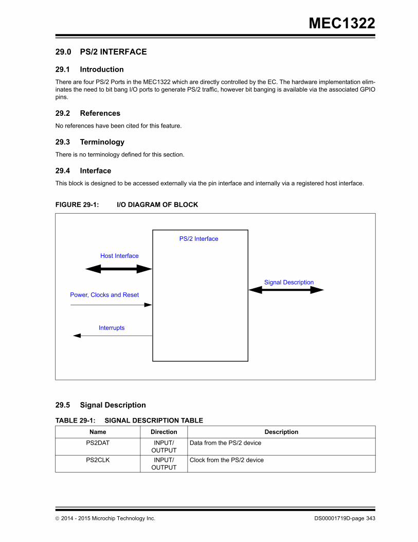
MEC1322
29.0 PS/2 INTERFACE
29.1 Introduction
There are four PS/2 Ports in the MEC1322 which are directly controlled by the EC. The hardware implementation elim-inates the need to bit bang I/O ports to generate PS/2 traffic, however bit banging is available via the associated GPIOpins.
29.2 References
No references have been cited for this feature.
29.3 Terminology
There is no terminology defined for this section.
29.4 Interface
This block is designed to be accessed externally via the pin interface and internally via a registered host interface.
29.5 Signal Description
FIGURE 29-1: I/O DIAGRAM OF BLOCK
TABLE 29-1: SIGNAL DESCRIPTION TABLE
Name Direction Description
PS2DAT INPUT/OUTPUT
Data from the PS/2 device
PS2CLK INPUT/OUTPUT
Clock from the PS/2 device
PS/2 Interface
Interrupts
Power, Clocks and Reset
Host Interface
Signal Description
2014 - 2015 Microchip Technology Inc. DS00001719D-page 343

MEC1322
29.6 Host Interface
The registers defined for the Keyboard Scan Interface are accessible by the various hosts as indicated in Section 29.15,"EC-Only Registers".
29.7 Power, Clocks and Reset
This section defines the Power, Clock, and Reset parameters of the block.
29.7.1 POWER DOMAINS
29.7.2 CLOCK INPUTS
29.7.3 RESETS
29.8 Interrupts
This section defines the Interrupt Sources generated from this block.
29.9 Low Power Modes
The PS/2 Interface may be put into a low power state by the chip’s Power, Clocks, and Reset (PCR) circuitry.
The PS2 interface will only sleep while the PS2 is disabled or in Rx mode with no traffic on the bus.
29.10 Description
Each EC PS/2 serial channels use a synchronous serial protocol to communicate with the auxiliary device. Each PS/2channel has Clock and Data signal lines. The signal lines are bi-directional and employ open drain outputs capable ofsinking 12m, as required by the PS/2 specification. A pull-up resistor, typically 10K, is connected to both lines. Thisallows either the EC PS/2 logic or the auxiliary device to drive the lines. Regardless of the drive source, the auxiliary
TABLE 29-2: POWER SOURCES
Name Description
VCC1 The logic and registers implemented in this block are powered by this power well.
TABLE 29-3: CLOCK INPUTS
Name Description
48 MHz Ring Oscillator This is the clock source for PS/2 Interface logic.
2 MHz Clock The PS/2 state machine is clocked using the 2 MHz clock.
TABLE 29-4: RESET SIGNALS
Name Description
VCC1_RESET This signal resets all the registers and logic in this block to their default state.
TABLE 29-5: EC INTERRUPTS
Source Description
PW2_x Interrupt request to the Interrupt Aggregator for PS2 controller instance x, based on PS2 controller activity. Section 29.15.4, "PS2 Status Register" defines the sources for the interrupt request.
PS2_x_WK Wake-up request to the Interrupt Aggregator’s wake-up interface for PS2 port x.
In order to enable PS2 wakeup interrupts, the pin control registers for the PS2DAT pin must be programmed to Input, Falling Edge Triggered, non-inverted polarity detection.
DS00001719D-page 344 2014 - 2015 Microchip Technology Inc.

MEC1322
device always provides the clock for transmit and receive operations. The serial packet is made up of eleven bits, listedin the order they appear on the data line: start bit, eight data bits (least significant bit first), odd parity, and stop bit. Eachbit cell is from 60μS to 100μS long.
All PS/2 Serial Channel signals (PS2CLK and PS2DAT) are driven by open drain drivers which can be pulled to VCC1or the main power rail (+3.3V nominal) through 10K-ohm resistors.
The PS/2 controller supports a PS/2 Wake Interface that can wake the EC from the IDLE or SLEEP states. The WakeInterface can generate wake interrupts without a clock. The PS/2 Wake Interface is only active when the peripheraldevice and external pull-up resisters are powered by the VCC1 supply.
There are no special precautions to be taken to prevent back drive of a PS/2 peripheral powered by the main power wellwhen the power well is off, as long as the external 10K pull-up resistor is tied to the same power source as the peripheral.
29.11 Block Diagram
29.12 PS/2 Port Physical Layer Byte Transmission Protocol
The PS/2 physical layer transfers a byte of data via an eleven bit serial stream as shown in Table 29-6. A logic 1 is sentat an active high level. Data sent from a Keyboard or mouse device to the host is read on the falling edge of the clocksignal. The Keyboard or mouse device always generates the clock signal. The Host may inhibit communication by pull-ing the Clock line low. The Clock line must be continuously high for at least 50 microseconds before the Keyboard ormouse device can begin to transmit its data. See Table 29-7, "PS/2 Port Physical Layer Bus States".
FIGURE 29-2: PORT PS/2 BLOCK DIAGRAM
TABLE 29-6: PS/2 PORT PHYSICAL LAYER BYTE TRANSMISSION PROTOCOL
Bit Function
1 Start bit (always 0)
2 Data bit 0 (least significant bit)
3 Data bit 1
4 Data bit 2
5 Data bit 3
6 Data bit 4
7 Data bit 5
8 Data bit 6
9 Data bit 7 (most significant bit)
10 Parity bit (odd parity)
11 Stop Bit (always 1)
Control Registers PS2DAT
PS2CLK
PS/2 Channel
State Machine
EC I/F
PS2_xinterrupt
48MHz
2 MHz
2014 - 2015 Microchip Technology Inc. DS00001719D-page 345
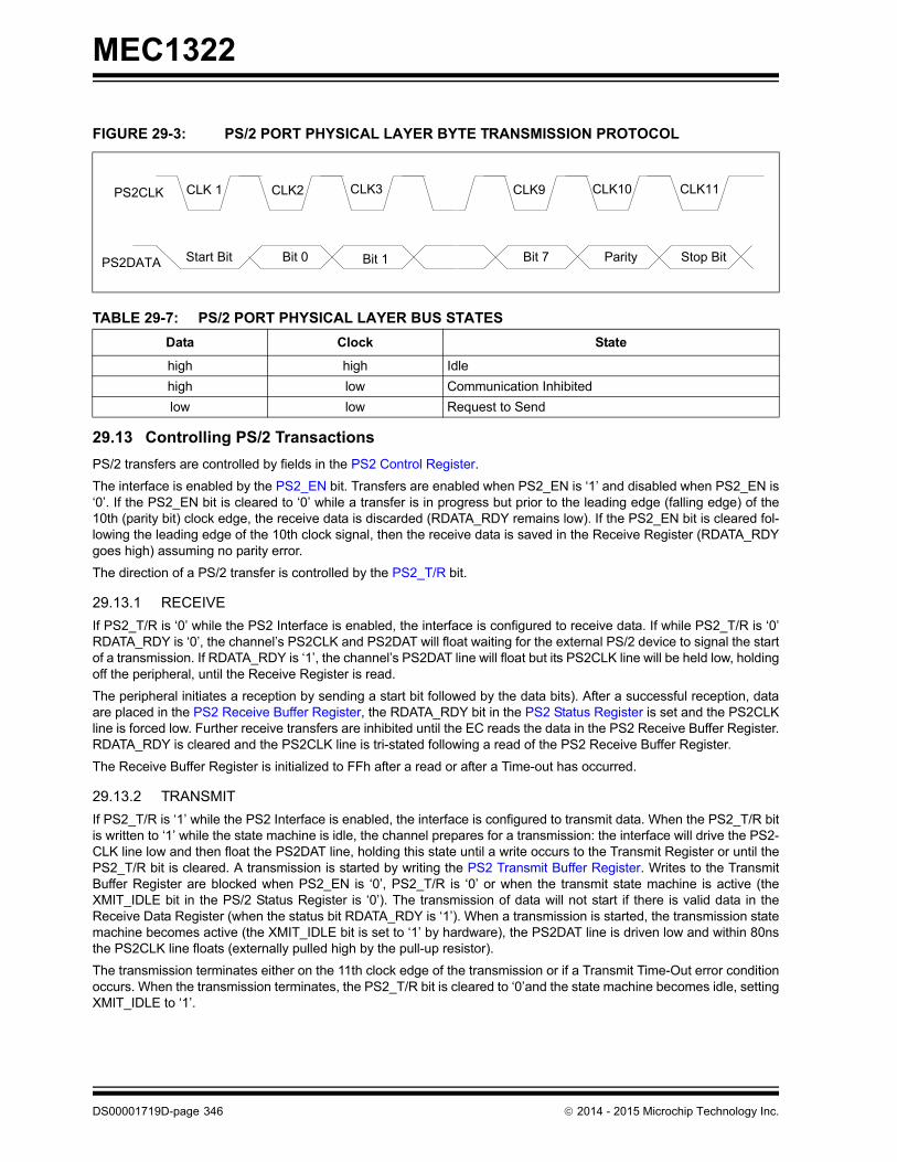
MEC1322
29.13 Controlling PS/2 Transactions
PS/2 transfers are controlled by fields in the PS2 Control Register.
The interface is enabled by the PS2_EN bit. Transfers are enabled when PS2_EN is ‘1’ and disabled when PS2_EN is‘0’. If the PS2_EN bit is cleared to ‘0’ while a transfer is in progress but prior to the leading edge (falling edge) of the10th (parity bit) clock edge, the receive data is discarded (RDATA_RDY remains low). If the PS2_EN bit is cleared fol-lowing the leading edge of the 10th clock signal, then the receive data is saved in the Receive Register (RDATA_RDYgoes high) assuming no parity error.
The direction of a PS/2 transfer is controlled by the PS2_T/R bit.
29.13.1 RECEIVE
If PS2_T/R is ‘0’ while the PS2 Interface is enabled, the interface is configured to receive data. If while PS2_T/R is ‘0’RDATA_RDY is ‘0’, the channel’s PS2CLK and PS2DAT will float waiting for the external PS/2 device to signal the startof a transmission. If RDATA_RDY is ‘1’, the channel’s PS2DAT line will float but its PS2CLK line will be held low, holdingoff the peripheral, until the Receive Register is read.
The peripheral initiates a reception by sending a start bit followed by the data bits). After a successful reception, dataare placed in the PS2 Receive Buffer Register, the RDATA_RDY bit in the PS2 Status Register is set and the PS2CLKline is forced low. Further receive transfers are inhibited until the EC reads the data in the PS2 Receive Buffer Register.RDATA_RDY is cleared and the PS2CLK line is tri-stated following a read of the PS2 Receive Buffer Register.
The Receive Buffer Register is initialized to FFh after a read or after a Time-out has occurred.
29.13.2 TRANSMIT
If PS2_T/R is ‘1’ while the PS2 Interface is enabled, the interface is configured to transmit data. When the PS2_T/R bitis written to ‘1’ while the state machine is idle, the channel prepares for a transmission: the interface will drive the PS2-CLK line low and then float the PS2DAT line, holding this state until a write occurs to the Transmit Register or until thePS2_T/R bit is cleared. A transmission is started by writing the PS2 Transmit Buffer Register. Writes to the TransmitBuffer Register are blocked when PS2_EN is ‘0’, PS2_T/R is ‘0’ or when the transmit state machine is active (theXMIT_IDLE bit in the PS/2 Status Register is ‘0’). The transmission of data will not start if there is valid data in theReceive Data Register (when the status bit RDATA_RDY is ‘1’). When a transmission is started, the transmission statemachine becomes active (the XMIT_IDLE bit is set to ‘1’ by hardware), the PS2DAT line is driven low and within 80nsthe PS2CLK line floats (externally pulled high by the pull-up resistor).
The transmission terminates either on the 11th clock edge of the transmission or if a Transmit Time-Out error conditionoccurs. When the transmission terminates, the PS2_T/R bit is cleared to ‘0’and the state machine becomes idle, settingXMIT_IDLE to ‘1’.
FIGURE 29-3: PS/2 PORT PHYSICAL LAYER BYTE TRANSMISSION PROTOCOL
TABLE 29-7: PS/2 PORT PHYSICAL LAYER BUS STATES
Data Clock State
high high Idle
high low Communication Inhibited
low low Request to Send
Start Bit Bit 0 ParityBit 7Bit 1 Stop Bit
CLK 1 CLK2 CLK9 CLK10 CLK11CLK3PS2CLK
PS2DATA
DS00001719D-page 346 2014 - 2015 Microchip Technology Inc.

MEC1322
The PS2_T/R bit must be written to a ‘1’ before initiating another transmission to the remote device. If the PS2_T/R bitis set to ‘1’ while the channel is actively receiving data (that is, while the status bit RDATA_RDYis ‘1’) prior to the leadingedge of the 10th (parity bit) clock edge, the receive data is discarded. If the bit is set after the 10th edge, the receivedata is saved in the Receive Register.
29.14 Instance Description
29.15 EC-Only Registers
The registers listed in the EC-Only Register Summary table are for a single instance of the PS/2 Interface. Theaddresses of each register listed in this table are defined as a relative offset to the host “Base Address” defined in theEC-Only Register Base Address Table.
The Base Address indicates where the first register can be accessed in a particular address space for a block instance.
29.15.1 PS2 TRANSMIT BUFFER REGISTER
TABLE 29-8: EC-ONLY REGISTER BASE ADDRESS TABLE
Block Instance Instance Number
Host Address Space Base Address
PS/2 Interface 0 EC 32-bit internal address space
4000_9000h
1 EC 32-bit internal address space
4000_9040h
2 EC 32-bit internal address space
4000_9080h
3 EC 32-bit internal address space
4000_90C0h
TABLE 29-9: EC-ONLY REGISTER SUMMARY
Offset Register Name
0h PS2 Transmit Buffer Register
0h PS2 Receive Buffer Register
4h PS2 Control Register
8h PS2 Status Register
Offset 00h
Bits Description Type DefaultReset Event
31:8 Reserved R - -
7:0 TRANSMIT_DATA
Writes to this register start a transmission of the data in this register to the peripheral.
W 0h VCC1_RESET
2014 - 2015 Microchip Technology Inc. DS00001719D-page 347

MEC1322
29.15.2 PS2 RECEIVE BUFFER REGISTER
29.15.3 PS2 CONTROL REGISTER
Offset 00h
Bits Description Type DefaultReset Event
31:8 Reserved R - -
7:0 RECEIVE_DATA
Data received from a peripheral are recorded in this register.
A transmission initiated by writing the PS2 Transmit Buffer Register will not start until valid data in this register have been read and RDATA_RDY has been cleared by hardware.
The Receive Buffer Register is initialized to FFh after a read or after a Time-out has occurred.
R FFh VCC1_RESET
Offset 00h
Bits Description Type DefaultReset Event
31:6 Reserved R - -
5:4 STOP
These bits are used to set the level of the stop bit expected by the PS/2 channel state machine. These bits are therefore only valid when PS2_EN is set.
00b=Receiver expects an active high stop bit.01b=Receiver expects an active low stop bit.10b=Receiver ignores the level of the Stop bit (11th bit is not inter-
preted as a stop bit).11b=Reserved.
R/W 0h VCC1_RESET
3:2 PARITY
These bits are used to set the parity expected by the PS/2 channel state machine. These bits are therefore only valid when PS2_EN is set.
00b=Receiver expects Odd Parity (default).01b=Receiver expects Even Parity.10b=Receiver ignores level of the parity bit (10th bit is not interpreted
as a parity bit).11b=Reserved
R/W 0h VCC1_RESET
1 PS2_EN
PS/2 Enable.
0=The PS/2 state machine is disabled. The CLK pin is driven low andthe DATA pin is tri-stated.
1=The PS/2 state machine is enabled, allowing the channel to per-form automatic reception or transmission, depending on thestate of PS2_T/R.
R/W 0h VCC1_RESET
0 PS2_T/R
PS/2 Transmit/Receive
0=The P2/2 channel is enabled to receive data. 1=The PS2 channel is enabled to transmit data.
R/W 0h VCC1_RESET
DS00001719D-page 348 2014 - 2015 Microchip Technology Inc.

MEC1322
Changing values in the PS2 CONTROL REGISTER at a rate faster than 2 MHz, may result in unpredictable behavior.
29.15.4 PS2 STATUS REGISTER
Offset 08h
Bits Description Type DefaultReset Event
31:8 Reserved R - -
7 XMIT_START_TIMEOUTTransmit Start Timeout.
0=No transmit start timeout detected1=A start bit was not received within 25 ms following the transmit start event. The transmit start bit time-out condition is also indicated by the XMIT_TIMEOUT bit.
R/WC 0h VCC1_RESET
6 RX_BUSYReceive Channel Busy.
0=The channel is actively receiving PS/2 data1=The channel is idle
R 0h VCC1_RESET
5 XMIT_TIME_OUTTransmitter Idle.
When the XMIT_TIMEOUT bit is set, the PS2_T/R bit is held clear, the PS/2 channel’s CLK line is pulled low for a minimum of 300μs until the PS/2 Status register is read. The XMIT_TIMEOUT bit is set on one of three transmit conditions: when the transmitter bit time (the time between falling edges) exceeds 300μs, when the transmit-ter start bit is not received within 25ms from signaling a transmit start event or if the time from the first bit (start) to the 10th bit (parity) exceeds 2ms
R/WC 0h VCC1_RESET
4 XMIT_IDLETransmitter Idle.
0=The channel is actively transmitting PS/2 data. Writing the PS2 Transmit Buffer Register will cause the XMIT_IDLE bit to clear 1=The channel is not transmitting. This bit transitions from ‘0’ to ‘1’ in the following cases:The falling edge of the 11th CLKXMIT_TIMEOUT is setThe PS2_T/R bit is clearedThe PS2_EN bit is cleared.
A low to high transition on this bit generates a PS2 Activity interrupt.
R 0h VCC1_RESET
3 FE Framing Error
When receiving data, the stop bit is clocked in on the falling edge of the 11th CLK edge. If the channel is configured to expect either a high or low stop bit and the 11th bit is contrary to the expected stop polarity, then the FE and REC_TIMEOUT bits are set following the falling edge of the 11th CLK edge and an interrupt is generated.
R/WC 0h VCC1_RESET
2014 - 2015 Microchip Technology Inc. DS00001719D-page 349

MEC1322
2 PEParity Error
When receiving data, the parity bit is clocked in on the falling edge of the 10th CLK edge. If the channel is configured to expect either even or odd parity and the 10th bit is contrary to the expected parity, then the PE and REC_TIMEOUT bits are set following the falling edge of the 10th CLK edge and an interrupt is generated.
R/WC 0h VCC1_RESET
1 REC_TIMEOUTReceive Timeout
Following assertion of the REC_TIMEOUT bit, the channel’s CLK line is automatically pulled low for a minimum of 300us until the PS/2 status register is read. Under PS2 automatic operation, PS2_EN is set, this bit is set on one of three receive error conditions:When the receiver bit time (the time between falling edges) exceeds 300μs.If the time from the first bit (start) to the 10th bit (parity) exceeds 2ms.On a receive parity error along with the Parity Error (PE) bit.On a receive framing error due to an incorrect STOP bit along with the framing error (FE) bit.
A low to high transition on this bit generates a PS2 Activity interrupt.
R/WC 0h VCC1_RESET
0 RDATA_RDYReceive Data Ready
Under normal operating conditions, this bit is set following the falling edge of the 11th clock given successful reception of a data byte from the PS/2 peripheral (i.e., no parity, framing, or receive time-out errors) and indicates that the received data byte is available to be read from the Receive Register. This bit may also be set in the event that the PS2_EN bit is cleared following the 10th CLK edge.
Reading the Receive Register clears this bit.
A low to high transition on this bit generates a PS2 Activity interrupt.
R 0h VCC1_RESET
Offset 08h
Bits Description Type DefaultReset Event
DS00001719D-page 350 2014 - 2015 Microchip Technology Inc.

MEC1322
30.0 KEYBOARD SCAN INTERFACE
30.1 Overview
The Keyboard Scan Interface block provides a register interface to the EC to directly scan an external keyboard matrixof size up to 18x8.
The maximum configuration of the Keyboard Scan Interface is 18 outputs by 8 inputs. For a smaller matrix size, firmwareshould configure unused KSO pins as GPIOs or another alternate function, and it should mask out unused KSIs andassociated interrupts.
30.2 References
No references have been cited for this feature.
30.3 Terminology
There is no terminology defined for this section.
30.4 Interface
This block is designed to be accessed externally via the pin interface and internally via a registered host interface.
30.5 Signal Description
FIGURE 30-1: I/O DIAGRAM OF BLOCK
TABLE 30-1: SIGNAL DESCRIPTION TABLE
Name Direction Description
KSI[7:0] Input Column inputs from external keyboard matrix.
KSO[17:0] Output Row outputs to external keyboard matrix.
Signal Description
Keyboard Scan Interface
Interrupts
Power, Clocks and Reset
Host Interface
2014 - 2015 Microchip Technology Inc. DS00001719D-page 351

MEC1322
30.6 Host Interface
The registers defined for the Keyboard Scan Interface are accessible by the various hosts as indicated in Section 30.11,"EC-Only Registers".
30.7 Power, Clocks and Reset
This section defines the Power, Clock, and Reset parameters of the block.
30.7.1 POWER DOMAINS
30.7.2 CLOCK INPUTS
30.7.3 RESETS
30.8 Interrupts
This section defines the Interrupt Sources generated from this block.
30.9 Low Power Modes
The Keyboard Scan Interface automatically enters a low power mode whenever it is not actively scanning the keyboardmatrix. The block is also placed in a low-power state when it is disabled by the KSEN bit. When the interface is in a low-power mode it will not prevent the chip from entering a sleep state. When the interface is active it will inhibit the chipsleep state until the interface has re-entered its low power mode.
TABLE 30-2: POWER SOURCES
Name Description
VCC1 The logic and registers implemented in this block are powered by this power well.
TABLE 30-3: CLOCK INPUTS
Name Description
48 MHz Ring Oscillator This is the clock source for Keyboard Scan Interface logic.
TABLE 30-4: RESET SIGNALS
Name Description
VCC1_RESET This signal resets all the registers and logic in this block to their default state.
TABLE 30-5: EC INTERRUPTS
Source Description
KSC_INT Interrupt request to the Interrupt Aggregator.
KSC_INT_WAKE Wake-up request to the Interrupt Aggregator’s wake-up interface.
DS00001719D-page 352 2014 - 2015 Microchip Technology Inc.
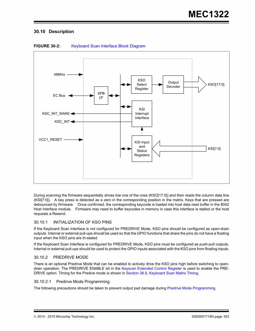
MEC1322
30.10 Description
During scanning the firmware sequentially drives low one of the rows (KSO[17:0]) and then reads the column data line(KSI[7:0]). A key press is detected as a zero in the corresponding position in the matrix. Keys that are pressed aredebounced by firmware. Once confirmed, the corresponding keycode is loaded into host data read buffer in the 8042Host Interface module. Firmware may need to buffer keycodes in memory in case this interface is stalled or the hostrequests a Resend.
30.10.1 INITIALIZATION OF KSO PINS
If the Keyboard Scan Interface is not configured for PREDRIVE Mode, KSO pins should be configured as open-drainoutputs. Internal or external pull-ups should be used so that the GPIO functions that share the pins do not have a floatinginput when the KSO pins are tri-stated.
If the Keyboard Scan Interface is configured for PREDRIVE Mode, KSO pins must be configured as push-pull outputs.Internal or external pull-ups should be used to protect the GPIO inputs associated with the KSO pins from floating inputs.
30.10.2 PREDRIVE MODE
There is an optional Predrive Mode that can be enabled to actively drive the KSO pins high before switching to open-drain operation. The PREDRIVE ENABLE bit in the Keyscan Extended Control Register is used to enable the PRE-DRIVE option. Timing for the Predive mode is shown in Section 38.9, Keyboard Scan Matrix Timing.
30.10.2.1 Predrive Mode Programming
The following precautions should be taken to prevent output pad damage during Predrive Mode Programming.
FIGURE 30-2: Keyboard Scan Interface Block Diagram
KSO Select
RegisterKSO[17:0]
KSI Input and
Status Registers
KSI[7:0]
KSI Interrupt Interface
Output Decoder
KSC_INT
KSC_INT_WAKE
48MHz
VCC1_RESET
SPBI/F
EC Bus
2014 - 2015 Microchip Technology Inc. DS00001719D-page 353

MEC1322
30.10.2.2 Asserting PREDRIVE_ENABLE
1. Disable Key Scan Interface (KSEN = '1')
2. Enable Predrive function (PREDRIVE_ENABLE = '1')
3. Program buffer type for all KSO pins to "push-pull”
4. Enable Keyscan Interface (KSEN ='0')
30.10.2.3 De-asserting PREDRIVE_ENABLE
1. Disable Key Scan Interface (KSEN = '1')
2. Program buffer type for all KSO pins to "open-drain”
3. Disable Predrive function (PREDRIVE_ENABLE = '0')
4. Enable Keyscan Interface (KSEN ='0')
30.10.3 INTERRUPT GENERATION
To support interrupt-based processing, an interrupt can optionally be generated on the high-to-low transition on any ofthe KSI inputs. A running clock is not required to generate interrupts.
30.10.3.1 Runtime interrupt
KSC_INT is the block’s runtime active-high level interrupt. It is connected to the interrupt interface of the Interrupt Aggre-gator, which then relays interrupts to the EC.
Associated with each KSI input is a status register bit and an interrupt enable register bit. A status bit is set when theassociated KSI input goes from high to low. If the interrupt enable bit for that input is set, an interrupt is generated. AnInterrupt is de-asserted when the status bit and/or interrupt enable bit is clear. A status bit cleared when written to a ‘1’.
Interrupts from individual KSIs are logically ORed together to drive the KSC_INT output port. Once asserted, an interruptis not asserted again until either all KSI[7:0] inputs have returned high or the has changed.
30.10.3.2 Wake-up Interrupt
KSC_INT_WAKE is the block’s wakeup interrupt. It is routed to the Interrupt Aggregator.
During sleep mode, i.e., when the bus clock is stopped, a high-to-low transition on any KSI whose interrupt enable bitis set causes the KSC_INT_WAKE to be asserted. Also set is the associated status bit in the EC Clock Required 2 StatusRegister (EC_CLK_REQ2_STS). KSC_WAKEUP_INT remains active until the bus clock is started.
The aforementioned transition on KSI also sets the corresponding status bit in the KSI STATUS Register. If enabled, aruntime interrupt is also asserted on KSC_INT when the bus clock resumes running.
30.10.4 WAKE PROGRAMMING
Using the Keyboard Scan Interface to ‘wake’ the MEC1322 can be accomplished using either the Keyboard Scan Inter-face wake interrupt, or using the wake capabilities of the GPIO Interface pins that are multiplexed with the KeyboardScan Interface pins. Enabling the Keyboard Scan Interface wake interrupt requires only a single interrupt enable accessand is recommended over using the GPIO Interface for this purpose.
30.11 EC-Only Registers
The registers listed in the EC-Only Register Summary table are for a single instance of the Keyboard Scan Interface.The addresses of each register listed in this table are defined as a relative offset to the host “Base Address” defined inthe EC-Only Register Base Address Table.
The Base Address indicates where the first register can be accessed in a particular address space for a block instance.
TABLE 30-6: EC-ONLY REGISTER BASE ADDRESS TABLE
Block InstanceInstance Number
Host Address Space Base Address
Keyboard ScanInterface
0 EC 32-bit internal address space
4000_9C00h
DS00001719D-page 354 2014 - 2015 Microchip Technology Inc.

MEC1322
30.11.1 KSO SELECT REGISTER
TABLE 30-7: EC-ONLY REGISTER SUMMARY
Offset Register Name
0h Reserved
4h KSO Select Register
8h KSI INPUT Register
Ch KSI STATUS Register
10h KSI INTERRUPT ENABLE Register
14h Keyscan Extended Control Register
Offset 04h
Bits Description Type DefaultReset Event
31:4 Reserved R - -
7 KSO_INVERT
This bit controls the output level of KSO pins when selected.
0= KSO[x] driven low when selected1= KSO[x] driven high when selected.
R/W 0b VCC1_RESET
6 KSEN
This field enables and disables keyboard scan
0= Keyboard scan enabled1= Keyboard scan disabled. All KSO output buffers disabled.
R/W 1h VCC1_RESET
5 KSO_ALL
0=When key scan is enabled, KSO output controlled by the KSO_SE-LECT field.
1=KSO[x] driven high when selected.
R/W 0b VCC1_RESET
4:0 KSO_SELECT
This field selects a KSO line (00000b = KSO[0] etc.) for output according to the value off KSO_INVERT in this register. See Table 30-8, "KSO Select Decode"
R/W 0h VCC1_RESET
TABLE 30-8: KSO SELECT DECODE
KSO Select [4:0] KSO Selected
00h KSO00
01h KSO01
02h KSO02
03h KSO03
04h KSO04
05h KSO05
06h KSO06
07h KSO07
08h KSO08
09h KSO09
0Ah KSO10
2014 - 2015 Microchip Technology Inc. DS00001719D-page 355

MEC1322
30.11.2 KSI INPUT REGISTER
30.11.3 KSI STATUS REGISTER
0Bh KSO11
0Ch KSO12
0Dh KSO13
0Eh KSO14
0Fh KSO15
10h KSO16
11h KSO17
TABLE 30-9: KEYBOARD SCAN OUT CONTROL SUMMARY
KSO_INVERTt KSEN KSO_ALL KSO_SELECT Description
X 1 x x Keyboard Scan disabled. KSO[17:0] output buffers disabled.
0 0 0 10001b-00000b KSO[Drive Selected] driven low. All others driven high
1 0 0 10001b-00000b KSO[Drive Selected] driven high. All others driven low
0 0 0 11111b-10010b All KSO’s driven high
1 0 0 11111b-10010b All KSO’s driven low
0 0 1 x All KSO’s driven high
1 0 1 x All KSO’s driven low
Offset 08h
Bits Description Type DefaultReset Event
31:8 Reserved R - -
7:0 KSI
This field returns the current state of the KSI pins.
R 0h VCC1_RESET
Offset 0Ch
Bits Description Type DefaultReset Event
31:8 Reserved R - -
7:0 KSI_STATUS
Each bit in this field is set on the falling edge of the corresponding KSI input pin.
A KSI interrupt is generated when its corresponding status bit and interrupt enable bit are both set. KSI interrupts are logically ORed together to produce KSC_INT and KSC_INT_WAKE.
Writing a ‘1’ to a bit will clear it. Writing a ‘0’ to a bit has no effect.
R/WC 0h VCC1_RESET
TABLE 30-8: KSO SELECT DECODE (CONTINUED)
KSO Select [4:0] KSO Selected
DS00001719D-page 356 2014 - 2015 Microchip Technology Inc.

MEC1322
30.11.4 KSI INTERRUPT ENABLE REGISTER
30.11.5 KEYSCAN EXTENDED CONTROL REGISTER
Offset 10h
Bits Description Type DefaultReset Event
31:8 Reserved R - -
7:0 KSI_INT_EN
Each bit in KSI_INT_EN enables interrupt generation due to high-to-low transition on a KSI input. An interrupt is generated when the cor-responding bits in KSI_STATUS and KSI_INT_EN are both set.
R/W 0h VCC1_RESET
Offset 14h
Bits Description Type Default Reset Event
32:1 Reserved R - -
0 PREDRIVE_ENABLE
PREDRIVE_ENABLE enables the PREDRIVE mode to actively drive the KSO pins high for approximately 100 ns before switching to open-drain operation.
0=Disable predrive on KSO pins1=Enable predrive on KSO pins.
RW 0 VCC1_RESET
2014 - 2015 Microchip Technology Inc. DS00001719D-page 357

MEC1322
31.0 BC-LINK MASTER
31.1 Overview
This block provides BC-Link connectivity to a slave device. The BC-Link protocol includes a start bit to signal thebeginning of a message and a turnaround (TAR) period for bus transfer between the Master and Companion devices.
31.2 References
No references have been cited for this feature.
31.3 Terminology
There is no terminology defined for this section.
31.4 Interface
This block is designed to be accessed externally via the pin interface and internally via a registered host interface.
31.5 Signal Description
FIGURE 31-1: I/O DIAGRAM OF BLOCK
TABLE 31-1: SIGNAL DESCRIPTION TABLE
Name Direction Description
BCM_CLK Output BC-Link output clock
BCM_DAT Input/Output Bidirectional data line
BCM_INT# Input Input from the companion device
Note: A weak pull-up resistor is recommended on the data line (100KΩ).
BC-Link Master
Interrupts
Power, Clocks and Reset
Interface Signal Description
DS00001719D-page 358 2014 - 2015 Microchip Technology Inc.

MEC1322
The maximum speed at which the BC-Link Master Interface can operate reliably depends on the drive strength of theBC-Link BCM_CLK and BCM_DAT pins, as well as the nature of the connection to the Companion device (over ribboncable or on a PC board). The following table shows the recommended maximum speeds over a PC board as well as a12 inch ribbon cable for selected drive strengths. The frequency is set with the BC-Link Clock Select Register.
31.6 Host Interface
The registers defined for the BC-Link Master Interface are accessible by the various hosts as indicated in Section 31.11,"EC-Only Registers".
31.7 Power, Clocks and Reset
31.7.1 POWER DOMAINS
31.7.2 CLOCK INPUTS
31.7.3 RESETS
31.8 Interrupts
This section defines the Interrupt Sources generated from this block.
TABLE 31-2: BC-LINK MASTER PIN DRIVE STRENGTH VS. FREQUENCY
Pin DriveStrength
Max Freqon PC Board
Min Value inBC-Link Clock Select
Register
Max Freqover Ribbon cable
Min Value in BC-Link Clock Select Register
16mA 24Mhz 1 16Mhz 2
TABLE 31-3: POWER SOURCES
Name Description
VCC1 The logic and registers implemented in this block are powered by this power well.
TABLE 31-4: CLOCK INPUTS
Name Description
48 MHz Ring Oscillator This is the clock source for Keyboard Scan Interface logic.
TABLE 31-5: RESET SIGNALS
Name Description
VCC1_RESET This signal resets all the registers and logic in this block to their default state.
TABLE 31-6: EC INTERRUPTS
Source Description
BCM_INT Busy Interrupt request to the Interrupt Aggregator, generated from the status event BUSYdefined in the BC-Link Status Register.
BCM_INT Err Interrupt request to the Interrupt Aggregator, generated from the status event defined in the BC-Link Status Register.
BC_INT_N_WK Wake-up request to the Interrupt Aggregator’s wake-up interface for BC-Link Master port.
In order to enable BC-Link wakeup interrupts, the pin control registers for the BC_INT# pin must be programmed to Input, Falling Edge Triggered, non-inverted polarity detection.
2014 - 2015 Microchip Technology Inc. DS00001719D-page 359

MEC1322
31.9 Low Power Modes
The BC-Link Master Interface automatically enters a low power mode whenever it is not active (that is, whenever theBUSY bit in the BC-Link Status Register is ‘0’). When the interface is in a low-power mode it will not prevent the chipfrom entering a sleep state. When the interface is active it will inhibit the chip sleep state until the interface has re-entered its low power mode.
31.10 Description
31.10.1 BC-LINK MASTER READ OPERATION
The BC-Link Read protocol requires two reads of the BC-Link Data Register. The two reads drive a two state-statemachine: the two states are Read#1 and Read#2. The Read#1 of the Data Register starts the read protocol on the BC-Link pins and sets the BUSY bit in the BC-Link Status Register. The contents of the data read during Read#1 by the ECis stale and is not to be used. After the BUSY bit in the BC-Link Status Register autonomously clears to ‘0’, the Read#2of the Data Register transfers the data read from the peripheral/BC-Link companion chip to the EC.
1. Software starts by checking the status of the BUSY bit in the Status Register. If the BUSY bit is ‘0’, proceed. IfBUSY is ‘1’, firmware must wait until it is ‘0’.
2. Software writes the address of the register to be read into the BC-Link Address Register.
3. Software then reads the Data Register. This read returns random data. The read activates the BC-Link Masterstate machine to transmit the read request packet to the BC-Link companion. When the transfer initiates, thehardware sets the BUSY bit to a ‘1’.
4. The BC-Link Companion reads the selected register and transmits the read response packet to the BC-Link Mas-ter. The Companion will ignore the read request if there is a CRC error; this will cause the Master state machineto time-out and issue a BC_ERR Interrupt.
FIGURE 31-2: BC-LINK MASTER BLOCK DIAGRAM
BC Bus Master IP
BCM_CLK
BCM_DAT
BCM_INT#
BC Status / ControlRegister
BC DataRegister
BC AddressRegister
External Pin interface
EC IF
Registers
Clock Divider
Bits
BC_BUSY_CLR
BC_ERR
Clock Generator
MCLK/2
MCLK/4
MCLK/8
∗∗∗
MCLK/63
MCLK=48MHz Ring Oscillator
∗∗∗
MCLK/Divider
DS00001719D-page 360 2014 - 2015 Microchip Technology Inc.

MEC1322
5. The Master state machine loads the Data Register, issues a BUSY Bit Clear interrupt and clears the BUSY bit to‘0’.
6. Software, after either receiving the Bit Clear interrupt, or polling the BUSY bit until it is ‘0’, checks the BC_ERRbit in the Status Register.
7. Software can now read the Data Register which contains the valid data if there was no BC Bus error.
8. If a Bus Error occurs, firmware must issue a soft reset by setting the RESET bit in the Status Register to ‘1’.
9. The read can re-tried once BUSY is cleared.
31.10.2 BC-LINK MASTER WRITE OPERATION
1. Software starts by checking the status of the BUSY bit in the BC-Link Status Register. If the BUSY bit is ‘0’, pro-ceed. If BUSY is ‘1’, firmware must wait until it is ‘0’.
2. Software writes the address of the register to be written into the BC-Link Address Register.
3. Software writes the data to be written into the addressed register in to the BC-Link Data Register.
4. The write to the Data Register starts the BC_Link write operation. The Master state machine sets the BUSY bit.
5. The BC-Link Master Interface transmits the write request packet.
6. When the write request packet is received by the BC-Link companion, the CRC is checked and data is written tothe addressed companion register.
7. The companion sends an ACK if the write is completed. A time-out will occur approximately 16 BC-Link clocksafter the packet is sent by the Master state machine. If a time-out occurs, the state machine will set the BC_ERRbit in the Status Register to ‘1’ approximately 48 clocks later and then clear the BUSY bit.
8. The Master state machine issues the Bit Clear interrupt and clears the BUSY bit after receiving the ACK from theCompanion
9. If a Bus Error occurs, firmware must issue a soft reset by setting the RESET bit in the Status Register to ‘1’.
10. The write can re-tried once BUSY is cleared.
31.11 EC-Only Registers
The registers listed in the EC-Only Register Summary table are for a single instance of the BC-Link Master interface.The addresses of each register listed in this table are defined as a relative offset to the host “Base Address” defined inthe EC-Only Register Base Address Table.
Note 31-1 The Base Address indicates where the first register can be accessed in a particular address spacefor a block instance.
Note: Steps 3 thorough 7 should be completed as a contiguous sequence. If not the interface could be presentingincorrect data when software thinks it is accessing a valid register read.
TABLE 31-7: EC-ONLY REGISTER BASE ADDRESS TABLE
Block InstanceInstance Number
Host Address Space Base Address (Note 31-1)
BC-LINK 0 EC 32-bit internal address space
4000_BC00h
TABLE 31-8: EC-ONLY REGISTER SUMMARY
Register Name EC Offset
BC-Link Status Register 00h
BC-Link Address Register 04h
BC-Link Data Register 08h
BC-Link Clock Select Register 0Ch
2014 - 2015 Microchip Technology Inc. DS00001719D-page 361

MEC1322
31.11.1 BC-LINK STATUS REGISTER
31.11.2 BC-LINK ADDRESS REGISTER
Offset 00h
Bits Description Type DefaultReset Event
31:4 Reserved R - -
7 RESET
When this bit is ‘1’the BC_Link Master Interface will be placed in reset and be held in reset until this bit is cleared to ‘0’. Setting RESET to ‘1’ causes the BUSY bit to be set to ‘1’. The BUSY remains set to ‘1’ until the reset operation of the BC Interface is com-pleted, which takes approximately 48 BC clocks.
The de-assertion of the BUSY bit on reset will not generate an inter-rupt, even if the BC_BUSY_CLR_INT_EN bit is ‘1’. The BUSY bit must be polled in order to determine when the reset operation has completed.
R/W 1h VCC1_RESET
6 BC_ERR
This bit indicates that a BC Bus Error has occurred. If an error occurs this bit is set by hardware when the BUSY bit is cleared. This bit is cleared when written with a ’1’. An interrupt is generated If this bit is ‘1’ and BC_ERR_INT_EN bit is ‘1’.Errors that cause this interrupt are:
• Bad Data received by the BASE (CRC Error) • Time-out caused by the COMPANION not responding.
All COMPANION errors cause the COMPANION to abort the opera-tion and the BASE to time-out.
R/WC 0h VCC1_RESET
5 BC_ERR_INT_EN
This bit is an enable for generating an interrupt when the BC_ERR bit is set by hardware. When this bit is ‘1’, the interrupt signal is enabled. When this bit is ‘0’, the interrupt is disabled.
R/W 0b VCC1_RESET
4 BC_BUSY_CLR_INT_EN
This bit is an enable for generating an interrupt when the BUSY bit inthis register is cleared by hardware. When this bit is set to ‘1’, theinterrupt signal is enabled. When the this bit is cleared to ‘0’, the inter-rupt is disabled. When enabled, the interrupt occurs after a BC Busread or write.
R/W 0h VCC1_RESET
3:1 Reserved R - -
0 BUSY
This bit is asserted to ‘1’ when the BC interface is transferring data and on reset. Otherwise it is cleared to ‘0’. When this bit is cleared by hardware, an interrupt is generated if the BC_BUSY_CL-R_INT_EN bit is set to ‘1’.
R 1h VCC1_RESET
Offset 04h
Bits Description Type DefaultReset Event
31:8 Reserved R - -
7:0 ADDRESS
Address in the Companion for the BC-Link transaction.
R/W 0h VCC1_RESET
DS00001719D-page 362 2014 - 2015 Microchip Technology Inc.

MEC1322
31.11.3 BC-LINK DATA REGISTER
31.11.4 BC-LINK CLOCK SELECT REGISTER
Offset 08h
Bits Description Type DefaultReset Event
31:8 Reserved R - -
7:0 DATA
As described in Section 31.10.1, "BC-Link Master READ Operation" and Section 31.10.2, "BC-Link Master WRITE Operation", this regis-ter hold data used in a BC-Link transaction.
R/W 0h VCC1_RESET
Offset 0Ch
Bits Description Type DefaultReset Event
31:8 Reserved R - -
7:0 DIVIDER
The BC Clock is set to the Master Clock divided by this field, or 48MHz/ (Divider +1). The clock divider bits can only can be changed when the BC Bus is in soft RESET (when either the Reset bit is set by software or when the BUSY bit is set by the interface).
Example settings for DIVIDER are shown in Table 31-9, "Example Frequency Settings".
R/W 4h VCC1_RESET
TABLE 31-9: EXAMPLE FREQUENCY SETTINGS
Divider Frequency
0 48MHz
1 24MHz
2 16MHz
3 12MHz
4 9.6MHz
15 2.18MHz
2A 1.12MHz
2014 - 2015 Microchip Technology Inc. DS00001719D-page 363
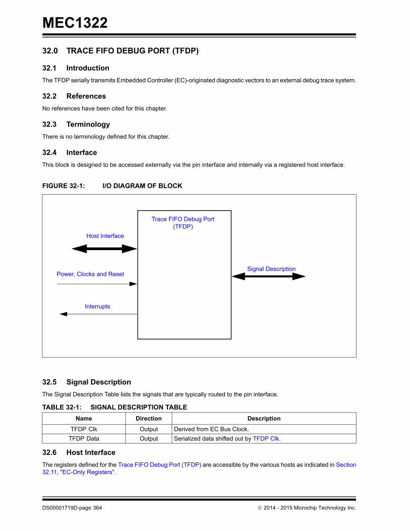
MEC1322
32.0 TRACE FIFO DEBUG PORT (TFDP)
32.1 Introduction
The TFDP serially transmits Embedded Controller (EC)-originated diagnostic vectors to an external debug trace system.
32.2 References
No references have been cited for this chapter.
32.3 Terminology
There is no terminology defined for this chapter.
32.4 Interface
This block is designed to be accessed externally via the pin interface and internally via a registered host interface.
32.5 Signal Description
The Signal Description Table lists the signals that are typically routed to the pin interface.
32.6 Host Interface
The registers defined for the Trace FIFO Debug Port (TFDP) are accessible by the various hosts as indicated in Section32.11, "EC-Only Registers".
FIGURE 32-1: I/O DIAGRAM OF BLOCK
TABLE 32-1: SIGNAL DESCRIPTION TABLE
Name Direction Description
TFDP Clk Output Derived from EC Bus Clock.
TFDP Data Output Serialized data shifted out by TFDP Clk.
Signal Description
Trace FIFO Debug Port (TFDP)
Interrupts
Power, Clocks and Reset
Host Interface
DS00001719D-page 364 2014 - 2015 Microchip Technology Inc.

MEC1322
32.7 Power, Clocks and Reset
This section defines the Power, Clock, and Reset parameters of the block.
32.7.1 POWER DOMAINS
32.7.2 CLOCK INPUTS
32.7.3 RESETS
32.8 Interrupts
There are no interrupts generated from this block.
32.9 Low Power Modes
The Trace FIFO Debug Port (TFDP) may be put into a low power state by the chip’s Power, Clocks, and Reset (PCR)circuitry.
32.10 Description
The TFDP is a unidirectional (from processor to external world) two-wire serial, byte-oriented debug interface for useby processor firmware to transmit diagnostic information.
The TFDP consists of the Debug Data Register, Debug Control Register, a Parallel-to-Serial Converter, a Clock/ControlInterface and a two-pin external interface (TFDP Clk, TFDP Data).
FIGURE 32-2: BLOCK DIAGRAM OF TFDP DEBUG PORT
TABLE 32-2: POWER SOURCES
Name Description
VCC1 This power well sources all of the registers and logic in this block.
TABLE 32-3: CLOCK INPUTS
Name Description
48 MHz Ring Oscillator This clock input is used to derive the TFDP Clk.
TABLE 32-4: RESET SIGNALS
Name Description
VCC1_RESET This reset signal resets all of the registers and logic in this block.
Data Register
PARALLEL-TO-SERIAL CONVERTER
CLOCK/CONTROL INTERFACE
WRITE_COMPLETE
MC
LK
TFDP_DAT
TFDP_CLK
2014 - 2015 Microchip Technology Inc. DS00001719D-page 365
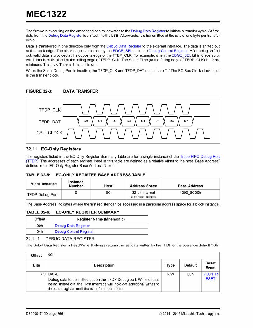
MEC1322
The firmware executing on the embedded controller writes to the Debug Data Register to initiate a transfer cycle. At first,data from the Debug Data Register is shifted into the LSB. Afterwards, it is transmitted at the rate of one byte per transfercycle.
Data is transferred in one direction only from the Debug Data Register to the external interface. The data is shifted outat the clock edge. The clock edge is selected by the EDGE_SEL bit in the Debug Control Register. After being shiftedout, valid data is provided at the opposite edge of the TFDP_CLK. For example, when the EDGE_SEL bit is ‘0’ (default),valid data is maintained at the falling edge of TFDP_CLK. The Setup Time (to the falling edge of TFDP_CLK) is 10 ns,minimum. The Hold Time is 1 ns, minimum.
When the Serial Debug Port is inactive, the TFDP_CLK and TFDP_DAT outputs are ‘1.’ The EC Bus Clock clock inputis the transfer clock.
FIGURE 32-3: DATA TRANSFER
32.11 EC-Only Registers
The registers listed in the EC-Only Register Summary table are for a single instance of the Trace FIFO Debug Port(TFDP). The addresses of each register listed in this table are defined as a relative offset to the host “Base Address”defined in the EC-Only Register Base Address Table.
The Base Address indicates where the first register can be accessed in a particular address space for a block instance.
32.11.1 DEBUG DATA REGISTER
The Debut Data Register is Read/Write. It always returns the last data written by the TFDP or the power-on default ‘00h’.
TABLE 32-5: EC-ONLY REGISTER BASE ADDRESS TABLE
Block Instance Instance Number Host Address Space Base Address
TFDP Debug Port 0 EC 32-bit internal address space
4000_8C00h
TABLE 32-6: EC-ONLY REGISTER SUMMARY
Offset Register Name (Mnemonic)
00h Debug Data Register
04h Debug Control Register
Offset 00h
Bits Description Type DefaultReset Event
7:0 DATA
Debug data to be shifted out on the TFDP Debug port. While data is being shifted out, the Host Interface will ‘hold-off’ additional writes to the data register until the transfer is complete.
R/W 00h VCC1_RESET
TFDP_CLK
TFDP_DAT
CPU_CLOCK
D0 D1 D2 D3 D4 D5 D6 D7
DS00001719D-page 366 2014 - 2015 Microchip Technology Inc.

MEC1322
32.11.2 DEBUG CONTROL REGISTER
Offset 04h
Bits Description Type DefaultReset Event
7 Reserved R - -
6:4 IP_DELAY
Inter-packet Delay. The delay is in terms of TFDP Debug output clocks. A value of 0 provides a 1 clock inter-packet period, while a value of 7 provides 8 clocks between packets:
R/W 000b VCC1_RESET
3:2 DIVSEL
Clock Divider Select. The TFDP Debug output clock is determined by this field, according to Table 32-7, "TFDP Debug Clocking":
R/W 00b VCC1_RESET
1 EDGE_SEL
1= Data is shifted out on the falling edge of the debug clock0= Data is shifted out on the rising edge of the debug clock (Default)
R/W 0b VCC1_RESET
0 EN
Enable.
1=Clock enabled0=Clock is disabled (Default)
R/W 0b VCC1_RESET
TABLE 32-7: TFDP DEBUG CLOCKING
divsel TFDP Debug Clock
00 24 MHz
01 12 MHz
10 6 MHz
11 Reserved
2014 - 2015 Microchip Technology Inc. DS00001719D-page 367
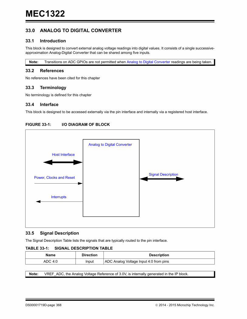
MEC1322
33.0 ANALOG TO DIGITAL CONVERTER
33.1 Introduction
This block is designed to convert external analog voltage readings into digital values. It consists of a single successive-approximation Analog-Digital Converter that can be shared among five inputs.
33.2 References
No references have been cited for this chapter
33.3 Terminology
No terminology is defined for this chapter
33.4 Interface
This block is designed to be accessed externally via the pin interface and internally via a registered host interface.
33.5 Signal Description
The Signal Description Table lists the signals that are typically routed to the pin interface.
Note: Transitions on ADC GPIOs are not permitted when Analog to Digital Converter readings are being taken.
FIGURE 33-1: I/O DIAGRAM OF BLOCK
TABLE 33-1: SIGNAL DESCRIPTION TABLE
Name Direction Description
ADC 4:0 Input ADC Analog Voltage Input 4:0 from pins
Note: VREF_ADC, the Analog Voltage Reference of 3.0V, is internally generated in the IP block.
Signal Description
Analog to Digital Converter
Interrupts
Power, Clocks and Reset
Host Interface
DS00001719D-page 368 2014 - 2015 Microchip Technology Inc.
MEC1322
33.6 Host Interface
The registers defined for the Trace FIFO Debug Port are accessible by the various hosts as indicated in Section 33.11,"EC-Only Registers".
33.7 Power, Clocks and Reset
This section defines the Power, Clock, and Reset parameters of the block.
33.7.1 POWER DOMAINS
33.7.2 CLOCK INPUTS
33.7.3 RESETS
33.8 Interrupts
33.9 Low Power Modes
The ADC may be put into a low power state by the chip’s Power, Clocks, and Reset (PCR) circuitry.
The ADC is designed to conserve power when it is either sleeping or disabled. It is disabled via the Activate Bit andsleeps when the ADC_SLEEP_EN signal is asserted. The sleeping state only controls clocking in the ADC and doesnot power down the analog circuitry. For lowest power consumption, the ADC Activate bit must be set to ‘0.’
TABLE 33-2: POWER SOURCES
Name Description
VCC1 This power well sources the registers tn this block.
AVCC This power well sources of the logic in this block, except where noted.
AVSS This is the ground signal for the block.
TABLE 33-3: CLOCK INPUTS
Name Description
1.2MHz This derived clock signal drives selected logic (1.2 MHz clock with a 50% duty cycle).
TABLE 33-4: RESET SIGNALS
Name Description
VCC1_RESET This reset signal resets all of the registers and logic in this block.
TABLE 33-5: EC INTERRUPTS
Source Description
ADC_Single_Int Interrupt signal from ADC controller to EC for Single-Sample ADC con-version.
ADC_Repeat_Int Interrupt signal from ADC controller to EC for Repeated ADC conversion.
Note: The ADC VREF must be powered down in order to get the lowest deep sleep current. The ADC VREFPower down bit, ADC_VREF_PD_REF is in the EC Subsystem Registers ADC VREF PD on page 381.
2014 - 2015 Microchip Technology Inc. DS00001719D-page 369

MEC1322
33.10 Description
The MEC1322 features a five channel successive approximation Analog to Digital Converter. The ADC architecture fea-tures excellent linearity and converts analog signals to 10 bit words. Conversion takes less than 12 microseconds per10-bit word. The five channels are implemented with a single high speed ADC fed by a five input analog multiplexer.The multiplexer cycles through the five voltage channels, starting with the lowest-numbered channel and proceeding tothe highest-number channel, selecting only those channels that are programmed to be active.
The input range on the voltage channels spans from 0V to the internal voltage reference. With an internal voltage ref-erence of 3.0V, this provides resolutions of 2.9mV. The range can easily be extended with the aid of resistor dividers.The accuracy of any voltage reading depends on the accuracy and stability of the voltage reference input.
The ADC conversion cycle starts either when the Start_Single bit in the ADC to set to 1 or when the ADC Repeat Timercounts down to 0. When the Start_Single is set to 1 the conversion cycle converts channels enabled by configurationbits in the ADC Single Register. When the Repeat Timer counts down to 0 the conversion cycle converts channelsenabled by configuration bits in the ADC Repeat Register. When both the Start_Single bit and the Repeat Timer requestconversions the Start_Single conversion is completed first.
Conversions always start with the lowest-numbered enabled channel and proceed to the highest-numbered enabledchannel.
33.10.1 REPEAT MODE
• Repeat Mode will start a conversion cycle of all ADC channels enabled by bits Rpt_En[4:0] in the ADC Repeat Register. The conversion cycle will begin after a delay determined by Start_Delay[15:0] in the ADC Delay Regis-ter.
FIGURE 33-2: ADC BLOCK DIAGRAM
Note: The ADC pins are 3.3V tolerant.
Note: If software repeatedly sets Start_Single to 1 at a rate faster than the Repeat Timer count down interval, theconversion cycle defined by the ADC Repeat Register will not be executed.
ADC BLOCK
ADC Reading Registers
ADC_Single_Int
Latch Control Logic
10-bit reading valuereadingHost Interface MUXADC
Control
Analog Inputs
(((
VREF
ADC_Repeat_Int
ADC_SLEEP_EN
ADC_CLK_REQ
DS00001719D-page 370 2014 - 2015 Microchip Technology Inc.

MEC1322
• After all channels enabled by Rpt_En[4:0] are complete, Repeat_Done_Status will be set to 1. This status bit is cleared when the next repeating conversion cycle begins to give a reflection of when the conversion is in prog-ress.
• As long as Start_Repeat is 1 the ADC will repeatedly begin conversion cycles with a period defined by Repeat_Delay[15:0].
• If the delay period expires and a conversion cycle is already in progress because Start_Single was written with a 1, the cycle in progress will complete, followed immediately by a conversion cycle using Rpt_En[4:0] to control the channel conversions.
33.10.2 SINGLE MODE
• The Single Mode conversion cycle will begin without a delay. After all channels enabled by Single_En[4:0] are complete, Single_Done_Status will be set to 1. When the next conversion cycle begins the bit is cleared.
• If Start_Single is written with a 1 while a conversion cycle is in progress because Start_Repeat is set, the conver-sion cycle will complete, followed immediately by a conversion cycle using Single_En[4:0] to control the channel conversions.
33.11 EC-Only Registers
The registers listed in the Table 33-7, "Analog to Digital Converter Register Summary" are for a single instance of theAnalog to Digital Converter block. The addresses of each register listed in this table are defined as a relative offset tothe host “Base Address” defined in Table 33-6, "Analog to Digital Converter Base Address Table".
Note 33-1 The Base Address indicates where the first register can be accessed in a particular address spacefor a block instance.
TABLE 33-6: ANALOG TO DIGITAL CONVERTER BASE ADDRESS TABLE
Instance NameInstance Number
Host Address Space Base Address (Note 33-1)
ADC 0 EC 32-bit internal address space
4000_7C00h
TABLE 33-7: ANALOG TO DIGITAL CONVERTER REGISTER SUMMARY
Offset Register Name (Mnemonic)
00h ADC Control Register
04h ADC Delay Register
08h ADC Status Register
0Ch ADC Single Register
10h ADC Repeat Register
14h ADC Channel 0 Reading Register
18h ADC Channel 1 Reading Register
1Ch ADC Channel 2 Reading Register
20h ADC Channel 3 Reading Register
24h ADC Channel 4 Reading Register
2014 - 2015 Microchip Technology Inc. DS00001719D-page 371

MEC1322
33.11.1 ADC CONTROL REGISTER
The ADC Control Register is used to control the behavior of the Analog to Digital Converter.
Offset 00h
Bits Description Type DefaultReset Event
31:8 RESERVED RES
7 Single_Done_Status
This bit is cleared when it is written with a 1. Writing a 0 to this bit has no effect.This bit can be used to generate an EC interrupt.
0: ADC single-sample conversion is not complete. This bit is cleared whenever an ADC conversion cycle begins for a single conversion cycle.1: ADC single-sample conversion is completed. This bit is set to 1 when all enabled channels in the single conversion cycle.
R/WC 0h VCC1_RESET
6 Repeat_Done_Status
This bit is cleared when it is written with a 1. Writing a 0 to this bit has no effect.This bit can be used to generate an EC interrupt.
0: ADC repeat-sample conversion is not complete. This bit is cleared whenever an ADC conversion cycle begins for a repeating conver-sion cycle.1: ADC repeat-sample conversion is completed. This bit is set to 1 when all enabled channels in a repeating conversion cycle com-plete.
R/WC 0h VCC1_RESET
5 RESERVED RES
4 Soft Reset
1: writing one causes a reset of the ADC block hardware (not the registers)0: writing zero takes the ADC block out of reset
R/W 0h VCC1_RESET
3 Power_Saver_Dis
0: Power saving feature is enabled. The Analog to Digital Converter controller powers down the ADC between conversion sequences.1: Power saving feature is disabled.
R/W 0h VCC1_RESET
2 Start_Repeat
0: The ADC Repeat Mode is disabled. Note: This setting will not ter-minate any conversion cycle in process, but will inhibit any further periodic conversions.1: The ADC Repeat Mode is enabled. This setting will start a conver-sion cycle of all ADC channels enabled by bits Rpt_En[4:0] in the ADC Repeat Register.
R/W 0h VCC1_RESET
1 Start_Single
0: The ADC Single Mode is disabled.1: The ADC Single Mode is enabled. This setting starts a single con-version cycle of all ADC channels enabled by bits Single_En[4:0] in the ADC Single Register.
Note: This bit is self-clearing
R/W 0h VCC1_RESET
DS00001719D-page 372 2014 - 2015 Microchip Technology Inc.
MEC1322
33.11.2 ADC DELAY REGISTER
The ADC Delay register determines the delay from setting Start_Repeat in the ADC Control Register and the start of aconversion cycle. This register also controls the interval between conversion cycles in repeat mode.
33.11.3 ADC STATUS REGISTER
The ADC Status Register indicates whether the ADC has completed a conversion cycle.
0 Activate
0: The ADC is disabled and placed in its lowest power state. Note: Any conversion cycle in process will complete before the block is shut down, so that the reading registers will contain valid data but no new conversion cycles will begin.1: ADC block is enabled for operation. Start_Single or Start_Repeat can begin data conversions by the ADC. Note: A reset pulse is sent to the ADC core when this bit changes from 0 to 1.
R/W 0h VCC1_RESET
Offset 04h
Bits Description Type DefaultReset Event
31:16 Repeat_Delay[15:0]
This field determines the interval between conversion cycles when Start_Repeat is 1. The delay is in units of 40μs. A value of 0 means no delay between conversion cycles, and a value of 0xFFFF means a delay of 2.6 seconds.This field has no effect when Start_Single is written with a 1.
R/W 0000h VCC1_RESET
15:0 Start_Delay[15:0]
This field determines the starting delay before a conversion cycle is begun when Start_Repeat is written with a 1. The delay is in units of 40μs. A value of 0 means no delay before the start of a conversion cycle, and a value of 0xFFFF means a delay of 2.6 seconds.This field has no effect when Start_Single is written with a 1.
R/W 0000h VCC1_RESET
Offset 08h
Bits Description Type DefaultReset Event
31:5 RESERVED RES
4:0 ADC_Ch_Status[4:0]
All bits are cleared by being written with a ‘1’.0: conversion of the corresponding ADC channel is not complete1: conversion of the corresponding ADC channel is completeNote: for enabled single cycles, the Single_Done_Status bit in the ADC Control Register is also set after all enabled channel conver-sion are done; for enabled repeat cycles, the Repeat_Done_Status in the ADC Control Register is also set after all enabled channel con-version are done.
R/WC 00h VCC1_RESET
Offset 00h
Bits Description Type DefaultReset Event
2014 - 2015 Microchip Technology Inc. DS00001719D-page 373

MEC1322
33.11.4 ADC SINGLE REGISTER
The ADC Single Register is used to control which ADC channel is captured during a Single-Sample conversion cycleinitiated by the Start_Single bit in the ADC Control Register.
APPLICATION NOTE: Do not change the bits in this register in the middle of a conversion cycle to insure properoperation.
33.11.5 ADC REPEAT REGISTER
The ADC Repeat Register is used to control which ADC channels are captured during a repeat conversion cycle initiatedby the Start_Repeat bit in the ADC Control Register.
33.11.6 ADC CHANNEL READING REGISTERS
All 5 ADC channels return their results into a 32-bit reading register. In each case the low 10 bits of the reading registerreturn the result of the Analog to Digital conversion and the upper 22 bits return 0. Table 33-7, “Analog to Digital Con-verter Register Summary,” on page 371 shows the addresses of all the reading registers.
Offset 0Ch
Bits Description Type DefaultReset Event
31:5 RESERVED RES
4:0 Single_En[4:0]
0: single cycle conversions for this channel are disabled1: single cycle conversions for this channel are enabledEach bit in this field enables the corresponding ADC channel when a single cycle of conversions is started when the Start_Single bit in the ADC Control Register is written with a 1.
R/W 00h VCC1_RESET
Offset 10h
Bits Description Type DefaultReset Event
31:5 RESERVED RES
4:0 Rpt_En[4:0]
0: repeat conversions for this channel are disabled1: repeat conversions for this channel are enabledEach bit in this field enables the corresponding ADC channel for each pass of the Repeated ADC Conversion that is controlled by bit Start_Repeat in the ADC Control Register.
R/W 00h VCC1_RESET
Note: The ADC Channel Reading Registers access require single 16, or 32 bit reads; i.e., two 8 bit reads cannotensure data coherency.
Offset See Table 33-7, "Analog to Digital Converter Register Summary"
Bits Description Type DefaultReset Event
31:10 RESERVED RES
9:0 ADCx_[9:0]
This read-only field reports the 10-bit output reading of the Input ADCx.
R/W 000h VCC1_RESET
DS00001719D-page 374 2014 - 2015 Microchip Technology Inc.

MEC1322
34.0 VBAT-POWERED RAM
34.1 Overview
The VBAT Powered RAM provides a 64 Byte Random Accessed Memory that is operational while the main power railis operational, and will retain its values powered by battery power while the main rail is unpowered.
34.2 References
No references have been cited for this feature.
34.3 Terminology
There is no terminology defined for this section.
34.4 Interface
This block is designed to be accessed externally via the pin interface and internally via a registered host interface.
34.5 Signal Description
There are no external signals for this block.
34.6 Host Interface
The registers defined for the Keyboard Scan Interface are accessible by the various hosts as indicated in Section 34.11,"Registers".
34.7 Power, Clocks and Reset
This section defines the Power, Clock, and Reset parameters of the block.
FIGURE 34-1: I/O DIAGRAM OF BLOCK
VBAT-Powered RAM
Interrupts
Power, Clocks and Reset
Host Interface
Signal Description
2014 - 2015 Microchip Technology Inc. DS00001719D-page 375
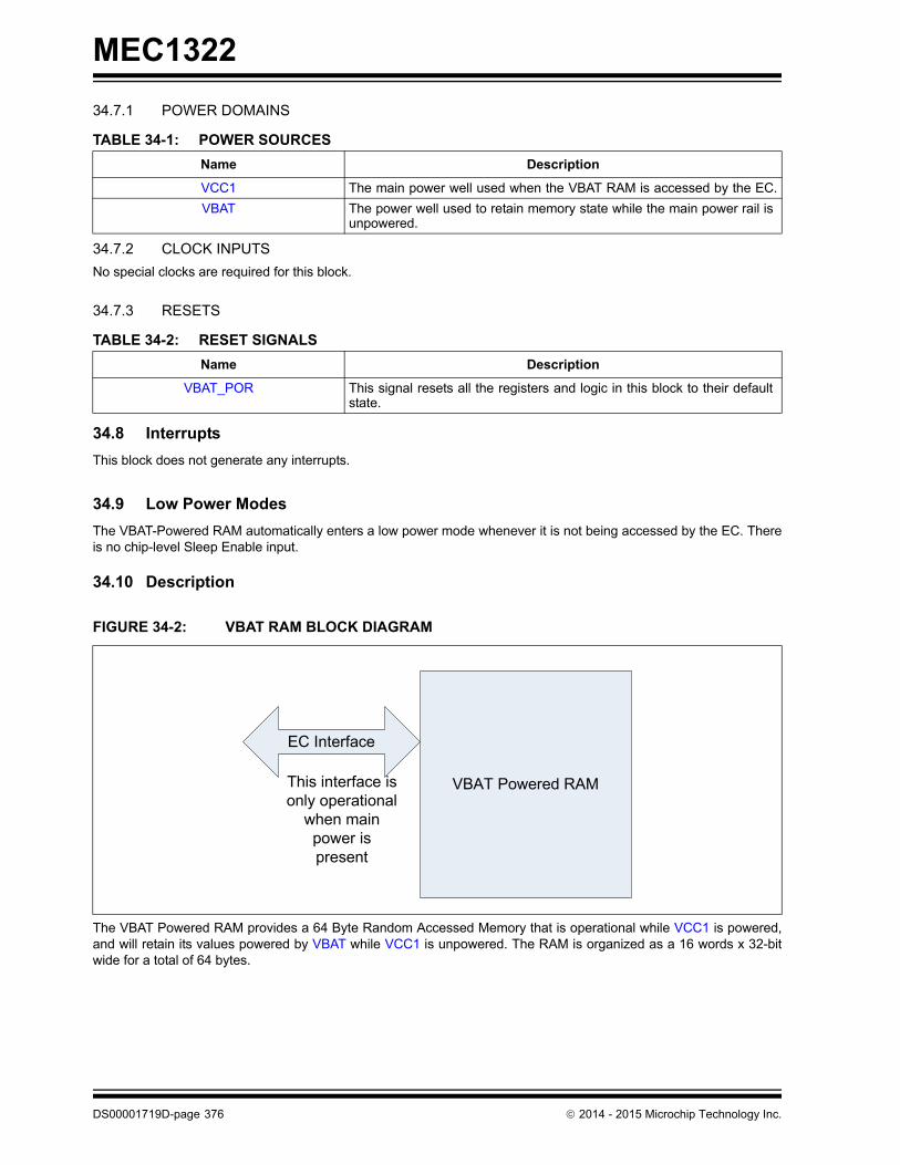
MEC1322
34.7.1 POWER DOMAINS
34.7.2 CLOCK INPUTS
No special clocks are required for this block.
34.7.3 RESETS
34.8 Interrupts
This block does not generate any interrupts.
34.9 Low Power Modes
The VBAT-Powered RAM automatically enters a low power mode whenever it is not being accessed by the EC. Thereis no chip-level Sleep Enable input.
34.10 Description
The VBAT Powered RAM provides a 64 Byte Random Accessed Memory that is operational while VCC1 is powered,and will retain its values powered by VBAT while VCC1 is unpowered. The RAM is organized as a 16 words x 32-bitwide for a total of 64 bytes.
TABLE 34-1: POWER SOURCES
Name Description
VCC1 The main power well used when the VBAT RAM is accessed by the EC.
VBAT The power well used to retain memory state while the main power rail is unpowered.
TABLE 34-2: RESET SIGNALS
Name Description
VBAT_POR This signal resets all the registers and logic in this block to their default state.
FIGURE 34-2: VBAT RAM BLOCK DIAGRAM
VBAT Powered RAM
EC Interface
This interface is only operational
when main power is present
DS00001719D-page 376 2014 - 2015 Microchip Technology Inc.

MEC1322
34.11 Registers
34.11.1 REGISTERS SUMMARY
The registers listed in the Table 34-3, "EC-Only Register Base Address Table" are for a single instance of the KeyboardScan Interface block. Each 32-bit RAM location is an offset from the EC base address.
Note 34-1 The Base Address indicates where the first register can be accessed in a particular address spacefor a block instance.
TABLE 34-3: EC-ONLY REGISTER BASE ADDRESS TABLE
Block InstanceInstance Number
Host Address Space Base Address (Note 34-1)
VBAT-Powered RAM 0 EC 32-bit internal address space
4000_A800h
2014 - 2015 Microchip Technology Inc. DS00001719D-page 377

MEC1322
35.0 EC SUBSYSTEM REGISTERS
35.1 Introduction
This chapter defines a bank of registers associated with the EC Subsystem.
35.2 References
None
35.3 Interface
This block is designed to be accessed internally by the EC via the register interface.
35.4 Power, Clocks and Reset
This section defines the Power, Clock, and Reset parameters of the block.
35.4.1 POWER DOMAINS
35.4.2 CLOCK INPUTS
This block does not require any special clock inputs. All register accesses are synchronized to the host clock.
35.4.3 RESETS
35.5 Interrupts
This block does not generate any interrupt events.
35.6 Low Power Modes
The EC Subsystem Registers may be put into a low power state by the chip’s Power, Clocks, and Reset (PCR) circuitry.When this block is commanded to sleep it will still allow read/write access to the registers.
35.7 Description
The EC Subsystem Registers block is a block implemented for aggregating miscellaneous registers required by theEmbedded Controller (EC) Subsystem that are not unique to a block implemented in the EC subsystem.
35.8 EC-Only Registers
Note 35-1 The Base Address indicates where the first register can be accessed in a particular address spacefor a block instance.
TABLE 35-1: POWER SOURCES
Name Description
VCC1 The EC Subsystem Registers are all implemented on this single power domain.
TABLE 35-2: RESET SIGNALS
Name Description
VCC1_RESET This reset signal, which is an input to this block, resets all the logic and registers to their initial default state.
TABLE 35-3: EC-ONLY REGISTER BASE ADDRESS TABLE
Block InstanceInstance Number
Host Address Space Base Address (Note 35-1)
EC_REG_BANK 0 EC 32-bit internal address space
4000_FC00h
DS00001719D-page 378 2014 - 2015 Microchip Technology Inc.

MEC1322
35.8.1 AHB ERROR CONTROL
35.8.2 INTERRUPT CONTROL
TABLE 35-4: RUNTIME REGISTER SUMMARY
Offset Register Name
04h MCHP Reserved
08h MCHP Reserved
0Ch MCHP Reserved
10h MCHP Reserved
14h AHB Error Control
18h Interrupt Control
1Ch ETM TRACE Enable
20h JTAG Enable
24h MCHP Reserved
28h WDT Event Count
2Ch MCHP Reserved
30h MCHP Reserved
34h MCHP Reserved
38h ADC VREF PD
3Ch MCHP Reserved
40h MCHP Reserved
Offset 14h
Bits Description Type DefaultReset Event
7:1 Reserved R - -
0 AHB_ERROR_DISABLE
0: EC memory exceptions are enabled.1: EC memory exceptions are disabled.
RW 0h VCC1_RESET
Offset 18h
Bits Description Type DefaultReset Event
31:1 Reserved R - -
0 NVIC_EN
This bit enables Alternate NVIC IRQ’s Vectors. The Alternate NVIC Vectors provides each interrupt event with a dedicated (direct) NVIC vector. 0 = Alternate NVIC vectors disabled1= Alternate NVIC vectors enabled
R/W 1b VCC1_RESET
2014 - 2015 Microchip Technology Inc. DS00001719D-page 379

MEC1322
35.8.3 ETM TRACE ENABLE
35.8.4 JTAG ENABLE
35.8.5 WDT EVENT COUNT
Offset 1Ch
Bits Description Type DefaultReset Event
31:1 Reserved R - -
0 TRACE_EN
This bit enables the ARM TRACE debug port (ETM/ITM). The Trace Debug Interface pins are forced to the TRACE functions.0 = ARM TRACE port disabled1= ARM TRACE port enabled
R/W 0b VCC1_RESET
Offset 20h
Bits Description Type DefaultReset Event
31:1 Reserved R - -
0 JTAG_EN
This bit enables the JTAG debug port. 0 = JTAG port disabled. JTAG cannot be enabled (i.e., the TRST# pin is ignored and the JTAG signals remain in their non-JTAG state).1= JTAG port enabled. A high on TRST# enables JTAG
R/W 0b VCC1_RESET
Offset 28h
Bits Description Type DefaultReset Event
31:4 Reserved R - -
3:0 WDT_COUNT
These EC R/W bits are cleared to 0 on VCC1 POR, but not on a WDT.
Note: This field is written by Boot ROM firmware to indicate thenumber of times a WDT fired before loading a good ECcode image.
R/W 0b VCC1_RESET
DS00001719D-page 380 2014 - 2015 Microchip Technology Inc.

MEC1322
35.8.6 ADC VREF PD
Offset 38h
Bits Description Type DefaultReset Event
31:1 Reserved R - -
0 ADC_VREF_PD_REF
ADC VREF Power down0=on1=off
R/W 0b VCC1_RESET
2014 - 2015 Microchip Technology Inc. DS00001719D-page 381

MEC1322
36.0 TEST MECHANISMS
36.1 Introduction
This section defines the XNOR Chain for board test.
Other test mechanisms for the ARM are described in Chapter 7.0, "ARM M4F Based Embedded Controller".
36.2 XNOR Chain
36.2.1 OVERVIEW
The XNOR Chain test mode provides a means to confirm that all MEC1322 pins are in contact with the motherboardduring assembly and test operations.
An example of an XNOR Chain test structure is illustrated below in 36.2.3Figure 36-1. When the XNOR Chain test modeis enabled all pins, except for the Excluded Pins shown in Section 36.2.2, are disconnected from their internal functionsand forced as inputs to the XNOR Chain. This allows a single input pin to toggle the XNOR Chain output if all otherinput pins are held high or low. The XNOR Chain output is the Test Output Pin, pin 17: KSO04/GPIO103/TFDP_-DATA/XNOR.
The tests that are performed when the XNOR Chain test mode is enabled require the board-level test hardware to con-trol the device pins and observe the results at the XNOR Chain output pin; e.g., as described in Section 36.2.3, "TestProcedure," on page 383.
36.2.2 EXCLUDED PINS
All pins in the pinout are included in the XNOR chain, except the following:
• Power Pins (VCC1, AVCC, VBAT, VREF_PECI)
• Ground Pins (VSS, AVSS, VSS_VBAT)
• CAP
• Crystal pins (XTAL1, XTAL2)
• Test Output Pin, pin 17: KSO04/GPIO103/TFDP_DATA/XNOR
• Test Port (JTAG_RST#, KSO02/GPIO101/JTAG_TDI, KSO03/GPIO102/JTAG_TDO, KSO01/GPIO100/JTAG_TMS, and KSO00/GPIO000/JTAG_TCK)
FIGURE 36-1: XNOR CHAIN TEST STRUCTURE
I/O#1 I/O#2 I/O#3 I/O#n XNOROut
DS00001719D-page 382 2014 - 2015 Microchip Technology Inc.

MEC1322
36.2.3 TEST PROCEDURE
36.2.3.1 Setup
Warning: Ensure power supply is off during Setup.1. Connect JTAG_RST# to ground.
2. Connect the VSS, AVSS, VSS_VBAT pins to ground.
3. Connect the VCC1, AVCC, VBAT pins to an unpowered 3.3V power source.
4. Connect the VREF_PECI pin to an unpowered 1.8V power source.
5. Connect an oscilloscope or voltmeter to the Test Output pin.
6. All other pins should be tied to ground.
36.2.3.2 Testing
1. Turn on the 3.3V power source.
2. Enable the XNOR Chain as defined in Section 36.2.3.3, "Procedure to Enable the XNOR Chain".
3. Bring one pin in the chain high. The output on the Test Output Pin, pin 17: KSO04/GPIO103/TFDP_-DATA/XNOR pin should toggle. Then individually toggle each of the remaining pins in the chain. Each time aninput pin is toggled either high or low the Test Output Pin, pin 17: KSO04/GPIO103/TFDP_DATA/XNOR pinshould toggle.
4. Once the XNOR test is completed, exit the XNOR Chain Test Mode by cycling VCC1 power.
36.2.3.3 Procedure to Enable the XNOR Chain
//BEGIN PROCEDURE TO ENTER XNOR CHAIN
///////////////////////////////////
//Reset Test Interface
///////////////////////////////////
force JTAG_RST# = 0
force KSO00/GPIO000/JTAG_TCK = 0
force KSO02/GPIO101/JTAG_TDI = 0
force KSO01/GPIO100/JTAG_TMS = 1
Wait 100 ns
////////////////////////////////
//Come out of reset
////////////////////////////////
force TRST#/JTAG_RST# = 1
Wait 100 ns
force KSO00/GPIO000/JTAG_TCK = 1
force KSO00/GPIO000/JTAG_TCK = 0
force KSO00/GPIO000/JTAG_TCK = 1
Note: There are 101 pins in the XNOR Chain.
Note: At this point all inputs to the XNOR Chain are low, except for the JTAG_RST# pin, and the output on theTest Output pin is non-inverted from its initial state, which is dependent on the number of pins in the chain.If the number of input pins in the chain is an even number, the initial state of the Test Output Pin, pin 17:KSO04/GPIO103/TFDP_DATA/XNOR is low. If the number of input pins in the chain is an odd number, theinitial state of the Test Output Pin, pin 17: KSO04/GPIO103/TFDP_DATA/XNOR is high.
2014 - 2015 Microchip Technology Inc. DS00001719D-page 383

MEC1322
force KSO00/GPIO000/JTAG_TCK = 0
force KSO00/GPIO000/JTAG_TCK = 1
force KSO00/GPIO000/JTAG_TCK = 0
force KSO00/GPIO000/JTAG_TCK = 1
force KSO00/GPIO000/JTAG_TCK = 0
////////////////////////////////
//Sequence 1
// Write IR with 7h
////////////////////////////////
force KSO00/GPIO000/JTAG_TCK = 1; //P
force KSO00/GPIO000/JTAG_TCK = 0; //1N
force KSO02/GPIO101/JTAG_TDI = 0
force KSO01/GPIO100/JTAG_TMS = 0
force KSO00/GPIO000/JTAG_TCK = 1; //P
force KSO00/GPIO000/JTAG_TCK = 0; //2N
force KSO02/GPIO101/JTAG_TDI = 0
force KSO01/GPIO100/JTAG_TMS = 1
force KSO00/GPIO000/JTAG_TCK = 1; //P
force KSO00/GPIO000/JTAG_TCK = 0; //3N
force KSO02/GPIO101/JTAG_TDI = 0
force KSO01/GPIO100/JTAG_TMS = 1
force KSO00/GPIO000/JTAG_TCK = 1; //P
force KSO00/GPIO000/JTAG_TCK = 0; //4N
force KSO02/GPIO101/JTAG_TDI = 0
force KSO01/GPIO100/JTAG_TMS = 0
force KSO00/GPIO000/JTAG_TCK = 1; //P
force KSO00/GPIO000/JTAG_TCK = 0; //5N
force KSO02/GPIO101/JTAG_TDI = 0
force KSO01/GPIO100/JTAG_TMS = 0
//////////////////////////////////////
//SHIFT IR 0x7h
/////////////////////////////////////
force KSO00/GPIO000/JTAG_TCK = 1; //P
force KSO00/GPIO000/JTAG_TCK = 0; //6N
force KSO02/GPIO101/JTAG_TDI = 1
force KSO01/GPIO100/JTAG_TMS = 0
force KSO00/GPIO000/JTAG_TCK = 1; //P
force KSO00/GPIO000/JTAG_TCK = 0; //7N
force KSO02/GPIO101/JTAG_TDI = 1
force KSO01/GPIO100/JTAG_TMS = 0
force KSO00/GPIO000/JTAG_TCK = 1; //P
force KSO00/GPIO000/JTAG_TCK = 0; //8N
DS00001719D-page 384 2014 - 2015 Microchip Technology Inc.

MEC1322
force KSO02/GPIO101/JTAG_TDI = 1
force KSO01/GPIO100/JTAG_TMS = 0
force KSO00/GPIO000/JTAG_TCK = 1; //P
force KSO00/GPIO000/JTAG_TCK = 0; //9N
force KSO02/GPIO101/JTAG_TDI = 0
force KSO01/GPIO100/JTAG_TMS = 1; //Next will be EXIT1_IR
force KSO00/GPIO000/JTAG_TCK = 1; //P
force KSO00/GPIO000/JTAG_TCK = 0; //10N
force KSO02/GPIO101/JTAG_TDI = 0
force KSO01/GPIO100/JTAG_TMS = 1; //Next will be UPDATE_IR
force KSO00/GPIO000/JTAG_TCK = 1; //P
force KSO00/GPIO000/JTAG_TCK = 0; //11N
force KSO02/GPIO101/JTAG_TDI = 0
force KSO01/GPIO100/JTAG_TMS = 0; //Next will be IDLE
force KSO00/GPIO000/JTAG_TCK = 1; //P
force KSO00/GPIO000/JTAG_TCK = 0; //12N
force KSO02/GPIO101/JTAG_TDI = 0
force KSO01/GPIO100/JTAG_TMS = 0; //Next will be IDLE
Wait 0 ns
//////////////////////////////////////////////////////////
// Sequence 2
// DIR=0, CMD[2:0]=1, DATA[7:0]=01\h, ADDR[7:0]=88\h
//////////////////////////////////////////////////////////
force KSO00/GPIO000/JTAG_TCK = 1; //P
force KSO00/GPIO000/JTAG_TCK = 0; //1N
force KSO02/GPIO101/JTAG_TDI = 0
force KSO01/GPIO100/JTAG_TMS = 1
force KSO00/GPIO000/JTAG_TCK = 1; //P
force KSO00/GPIO000/JTAG_TCK = 0; //2N
force KSO02/GPIO101/JTAG_TDI = 0
force KSO01/GPIO100/JTAG_TMS = 0
force KSO00/GPIO000/JTAG_TCK = 1; //P
force KSO00/GPIO000/JTAG_TCK = 0; //3N
force KSO02/GPIO101/JTAG_TDI = 0
force KSO01/GPIO100/JTAG_TMS = 0
///////////////////////////////////////////
//DIR 0 - Write
//////////////////////////////////////////
force KSO00/GPIO000/JTAG_TCK = 1; //P
force KSO00/GPIO000/JTAG_TCK = 0; //N (DR1)
force KSO02/GPIO101/JTAG_TDI = 0
force KSO01/GPIO100/JTAG_TMS = 0
2014 - 2015 Microchip Technology Inc. DS00001719D-page 385

MEC1322
///////////////////////////////////////////
//CMD 1 - Test
//////////////////////////////////////////
force KSO00/GPIO000/JTAG_TCK = 1; //P
**Verify KSO03/GPIO102/JTAG_TDO = 1//`TP_GPIO102.Check(1);
force KSO00/GPIO000/JTAG_TCK = 0; //N (DR2)
force KSO02/GPIO101/JTAG_TDI = 1
force KSO01/GPIO100/JTAG_TMS = 0
force KSO00/GPIO000/JTAG_TCK = 1; //P
**Verify KSO03/GPIO102/JTAG_TDO = 1//`TP_GPIO102.Check(1);
force KSO00/GPIO000/JTAG_TCK = 0; //N (DR3)
force KSO02/GPIO101/JTAG_TDI = 0
force KSO01/GPIO100/JTAG_TMS = 0
force KSO00/GPIO000/JTAG_TCK = 1; //P
**Verify KSO03/GPIO102/JTAG_TDO = 1//`TP_GPIO102.Check(1);
force KSO00/GPIO000/JTAG_TCK = 0; //N (DR4)
force KSO02/GPIO101/JTAG_TDI = 0
force KSO01/GPIO100/JTAG_TMS = 0
///////////////////////////////////////////
//DATA 0x01 - XNOR_EN
//////////////////////////////////////////
force KSO00/GPIO000/JTAG_TCK = 1; //P
**Verify KSO03/GPIO102/JTAG_TDO = 1//`TP_GPIO102.Check(1);
force KSO00/GPIO000/JTAG_TCK = 0; //N (DR5)
force KSO02/GPIO101/JTAG_TDI = 1
force KSO01/GPIO100/JTAG_TMS = 0
force KSO00/GPIO000/JTAG_TCK = 1; //P
**Verify KSO03/GPIO102/JTAG_TDO = 1//`TP_GPIO102.Check(1);
force KSO00/GPIO000/JTAG_TCK = 0; //N (DR6)
force KSO02/GPIO101/JTAG_TDI = 0
force KSO01/GPIO100/JTAG_TMS = 0
force KSO00/GPIO000/JTAG_TCK = 1; //P
**Verify KSO03/GPIO102/JTAG_TDO = 0//`TP_GPIO102.Check(0);
force KSO00/GPIO000/JTAG_TCK = 0; //N (DR7)
force KSO02/GPIO101/JTAG_TDI = 0
force KSO01/GPIO100/JTAG_TMS = 0
force KSO00/GPIO000/JTAG_TCK = 1; //P
**Verify KSO03/GPIO102/JTAG_TDO = 0//`TP_GPIO102.Check(0);
force KSO00/GPIO000/JTAG_TCK = 0; //N (DR8)
force KSO02/GPIO101/JTAG_TDI = 0
force KSO01/GPIO100/JTAG_TMS = 0
force KSO00/GPIO000/JTAG_TCK = 1; //P
DS00001719D-page 386 2014 - 2015 Microchip Technology Inc.

MEC1322
**Verify KSO03/GPIO102/JTAG_TDO = 0//`TP_GPIO102.Check(0);
force KSO00/GPIO000/JTAG_TCK = 0; //N (DR9)
force KSO02/GPIO101/JTAG_TDI = 0
force KSO01/GPIO100/JTAG_TMS = 0
force KSO00/GPIO000/JTAG_TCK = 1; //P
**Verify KSO03/GPIO102/JTAG_TDO = 1//`TP_GPIO102.Check(1);
force KSO00/GPIO000/JTAG_TCK = 0; //N (DR10)
force KSO02/GPIO101/JTAG_TDI = 0
force KSO01/GPIO100/JTAG_TMS = 0
force KSO00/GPIO000/JTAG_TCK = 1; //P
**Verify KSO03/GPIO102/JTAG_TDO = 0//`TP_GPIO102.Check(0);
force KSO00/GPIO000/JTAG_TCK = 0; //N (DR11)
force KSO02/GPIO101/JTAG_TDI = 0
force KSO01/GPIO100/JTAG_TMS = 0
force KSO00/GPIO000/JTAG_TCK = 1; //P
**Verify KSO03/GPIO102/JTAG_TDO = 0//`TP_GPIO102.Check(0);
force KSO00/GPIO000/JTAG_TCK = 0; //N (DR12)
force KSO02/GPIO101/JTAG_TDI = 0
force KSO01/GPIO100/JTAG_TMS = 0
//////////////////////////////////////////////////////////////
//ADDRESS 0x88 - Customer Control
/////////////////////////////////////////////////////////////
force KSO00/GPIO000/JTAG_TCK = 1; //P
**Verify KSO03/GPIO102/JTAG_TDO = 0//`TP_GPIO102.Check(0);
force KSO00/GPIO000/JTAG_TCK = 0; //N (DR13)
force KSO02/GPIO101/JTAG_TDI = 0
force KSO01/GPIO100/JTAG_TMS = 0
force KSO00/GPIO000/JTAG_TCK = 1; //P
**Verify KSO03/GPIO102/JTAG_TDO = 1//`TP_GPIO102.Check(1);
force KSO00/GPIO000/JTAG_TCK = 0; //N (DR14)
force KSO02/GPIO101/JTAG_TDI = 0
force KSO01/GPIO100/JTAG_TMS = 0
force KSO00/GPIO000/JTAG_TCK = 1; //P
**Verify KSO03/GPIO102/JTAG_TDO = 0//`TP_GPIO102.Check(0);
force KSO00/GPIO000/JTAG_TCK = 0; //N (DR15)
force KSO02/GPIO101/JTAG_TDI = 0
force KSO01/GPIO100/JTAG_TMS = 0
force KSO00/GPIO000/JTAG_TCK = 1; //P
**Verify KSO03/GPIO102/JTAG_TDO = 0//`TP_GPIO102.Check(0);
force KSO00/GPIO000/JTAG_TCK = 0; //N (DR16)
force KSO02/GPIO101/JTAG_TDI = 1
force KSO01/GPIO100/JTAG_TMS = 0
force KSO00/GPIO000/JTAG_TCK = 1; //P
2014 - 2015 Microchip Technology Inc. DS00001719D-page 387

MEC1322
**Verify KSO03/GPIO102/JTAG_TDO = 0//`TP_GPIO102.Check(0);
force KSO00/GPIO000/JTAG_TCK = 0; //N (DR17)
force KSO02/GPIO101/JTAG_TDI = 0
force KSO01/GPIO100/JTAG_TMS = 0
force KSO00/GPIO000/JTAG_TCK = 1; //P
**Verify KSO03/GPIO102/JTAG_TDO = 1//`TP_GPIO102.Check(1);
force KSO00/GPIO000/JTAG_TCK = 0; //N (DR18)
force KSO02/GPIO101/JTAG_TDI = 0
force KSO01/GPIO100/JTAG_TMS = 0
force KSO00/GPIO000/JTAG_TCK = 1; //P
**Verify KSO03/GPIO102/JTAG_TDO = 0//`TP_GPIO102.Check(0);
force KSO00/GPIO000/JTAG_TCK = 0; //N (DR19)
force KSO02/GPIO101/JTAG_TDI = 0
force KSO01/GPIO100/JTAG_TMS = 0
force KSO00/GPIO000/JTAG_TCK = 1; //P
**Verify KSO03/GPIO102/JTAG_TDO = 0//`TP_GPIO102.Check(0);
force KSO00/GPIO000/JTAG_TCK = 0; //N (DR20)
force KSO02/GPIO101/JTAG_TDI = 1
force KSO01/GPIO100/JTAG_TMS = 1
force KSO00/GPIO000/JTAG_TCK = 1; //P
**Verify KSO03/GPIO102/JTAG_TDO = 0//`TP_GPIO102.Check(0);
force KSO00/GPIO000/JTAG_TCK = 0; //N (E1_DR)
force KSO02/GPIO101/JTAG_TDI = 0
force KSO01/GPIO100/JTAG_TMS = 1
force KSO00/GPIO000/JTAG_TCK = 1; //P
force KSO00/GPIO000/JTAG_TCK = 0; //N (UP_DR)
force KSO02/GPIO101/JTAG_TDI = 0
force KSO01/GPIO100/JTAG_TMS = 0
force KSO00/GPIO000/JTAG_TCK = 1; //P
force KSO00/GPIO000/JTAG_TCK = 0; //N (EXTRA CLK)
force KSO02/GPIO101/JTAG_TDI = 0
force KSO01/GPIO100/JTAG_TMS = 0
force KSO00/GPIO000/JTAG_TCK = 1; //P
force KSO00/GPIO000/JTAG_TCK = 0; //N (EXTRA CLK)
force KSO02/GPIO101/JTAG_TDI = 0
force KSO01/GPIO100/JTAG_TMS = 0
Wait 100 ns
////////////////////////////////////////////////////////////////////////////
//FINISHED PROCEDURE TO ENTER XNOR
///////////////////////////////////////////////////////////////////////////
DS00001719D-page 388 2014 - 2015 Microchip Technology Inc.

MEC1322
37.0 ELECTRICAL SPECIFICATIONS
37.1 Maximum Ratings*
*Stresses exceeding those listed could cause permanent damage to the device. This is a stress rating only and func-tional operation of the device at any other condition above those indicated in the operation sections of this specificationis not implied.
37.1.1 ABSOLUTE MAXIMUM THERMAL RATINGS
37.1.2 ABSOLUTE MAXIMUM SUPPLY VOLTAGE RATINGS
37.1.3 ABSOLUTE MAXIMUM I/O VOLTAGE RATINGS
Note 37-1 The Power Supply used to power the buffer is shown in the Signal Power Well column of the PinMultiplexing Tables in Section 1.0 “Pin Configuration”.
37.2 Operational Specifications
37.2.1 POWER SUPPLY OPERATIONAL CHARACTERISTICS
Note: When powering this device from laboratory or system power supplies, it is important that the Absolute Max-imum Ratings not be exceeded or device failure can result. Some power supplies exhibit voltage spikes ontheir outputs when the AC power is switched on or off. In addition, voltage transients on the AC power linemay appear on the DC output. If this possibility exists, it is suggested that a clamp circuit be used.
TABLE 37-1: ABSOLUTE MAXIMUM THERMAL RATINGS
Parameter Maximum Limits
Operating Temperature Range 0oC to +70oC Commercial-40oC to +85oC Industrial
Storage Temperature Range -55o to +150oC
Lead Temperature Range Refer to JEDEC Spec J-STD-020B
TABLE 37-2: ABSOLUTE POWER SUPPLY RATINGS
Symbol Parameter Maximum Limits
VBAT 3.0V Battery Backup Power Supply with respect to ground -0.3V to +3.63V
VCC1 3.3V Suspend Power Supply with respect to ground -0.3V to +3.63V
VCC2 3.3V Main Power Supply with respect to ground -0.3V to +3.63V
Parameter Maximum Limits
Voltage with respect to ground on any pin without back-drive protection
-0.3V to (Power Supply used to power the buffer) + 0.3V (Note 37-1)
TABLE 37-3: POWER SUPPLY OPERATING CONDITIONS
Symbol Parameter MIN TYP MAX Units
VBAT Battery Backup Power Supply 2.0 3.0 3.6 V
VCC1 Suspend Power Supply 3.135 3.3 3.465 V
Note: The specification for the VCC1 supply is +/- 5%.
2014 - 2015 Microchip Technology Inc. DS00001719D-page 389

MEC1322
37.2.2 AC ELECTRICAL SPECIFICATIONS
The clock rise and fall times use the standard input thresholds of 0.8V and 2.0V unless otherwise specified and thecapacitive values listed in Section 37.2.2, "AC Electrical Specifications," on page 390.
37.2.3 CAPACITIVE LOADING SPECIFICATIONS
The following table defines the maximum capacitive load validated for the buffer characteristics listed in Table 37-4, “DCElectrical Characteristics,” on page 391.
CAPACITANCE TA = 25°C; fc = 1MHz; Vcc = 3.3 VDC
Note 37-2 The PCI buffers are designed to meet the defined PCI Local Bus Specification, Rev. 2.1, electricalrequirements.
Note 37-3 All input buffers can be characterized by this capacitance unless otherwise specified.
Note 37-4 All output buffers can be characterized by this capacitance unless otherwise specified.
Note: All output pins, except pin under test, tied to AC ground.
Parameter SymbolLimits
Unit NotesMIN TYP MAX
Input Capacitance of PCI_I and PCI_IO pins
CIN Note 37-2 pF
Input Capacitance of PCI_CLK pin CIN Note 37-2 pF
Output Load Capacitance supported by PCI_IO, PCI_O, and PCI_OD
COUT Note 37-2 pF
SUSCLK Input Capacitance CIN 10 pF
Input Capacitance of PECI_I and PECI_IO
CIN 10 pF
Output Load Capacitance supported by PECI_IO and OD_PH
COUT 10 pF
Input Capacitance (all other input pins)
CIN 10 pF Note 37-3
Output Capacitance (all other output pins)
COUT 20 pF Note 37-4
DS00001719D-page 390 2014 - 2015 Microchip Technology Inc.

MEC1322
37.2.4 DC ELECTRICAL CHARACTERISTICS FOR I/O BUFFERS
TABLE 37-4: DC ELECTRICAL CHARACTERISTICS
Parameter Symbol MIN TYP MAX Units Comments
PIO Type Buffer
All PIO Buffers
Pull-up current
Pull-down current
IPU
IPD
39
39
84
65
162
105
μA
μA
Internal PU/PD selected via the GPIO Pin Control Register.
I Type Input Buffer
Low Input Level
High Input Level
Tolerance
Schmitt Trigger Hyster-esis
VILI
VIHI
VHYS
0.7x VCC1
400
0.3x VCC1
3.63
V
V
V
mV
TTL Compatible Schmitt Trigger Input
This buffer is not 5V tolerant.
O-2 mA Type Buffer
Low Output Level
High Output Level
Tolerance
VOL
VOH VCC1-0.4
0.4 V
V
IOL = 2 mA
IOH = -2 mA
This buffer is not 5V tolerant.
IO-2 mA Type Buffer _ _ _ _ _ Same characteristics as an I and an O-2mA.
OD-2 mA Type Buffer
Low Output Level
Tolerance
VOL 0.4 V VOL = 2 mA
This buffer is not 5V tolerant.
IOD-2 mA Type Buffer _ _ _ _ _ Same characteristics as an I and an OD-2mA.
O-4 mA Type Buffer
Low Output Level
High Output Level
Tolerance
VOL
VOH VCC1-0.4
0.4 V
V
IOL = 4 mA
IOH = -4 mA
This buffer is not 5V tolerant.
IO-4 mA Type Buffer _ _ _ _ _ Same characteristics as an I and an O-4mA.
OD-4 mA Type Buffer
Low Output Level
Tolerance
VOL 0.4 V VOL = 4 mA
This buffer is not 5V tolerant.
IOD-4 mA Type Buffer _ _ _ _ _ Same characteristics as an I and an OD-4mA.
2014 - 2015 Microchip Technology Inc. DS00001719D-page 391

MEC1322
O-8 mA Type Buffer
Low Output Level
High Output Level
Tolerance
VOL
VOH VCC1-0.4
0.4 V
V
IOL = 8 mA
IOH = -8 mA
This buffer is not 5V tolerant.
IO-8 mA Type Buffer _ _ _ _ _ Same characteristics as an I and an O-8mA.
OD-8 mA Type Buffer
Low Output Level
Tolerance
VOL 0.4 V VOL = 8 mA
This buffer is not 5V tolerant.
IOD-8 mA Type Buffer _ _ _ _ _ Same characteristics as an I and an OD-8mA.
O-12 mA Type Buffer
Low Output Level
High Output Level
Tolerance
VOL
VOH VCC1-0.4
0.4 V
V
IOL = 12mA
IOH = -12mA
This buffer is not 5V tolerant.
IO-12 mA Type Buffer _ _ _ _ _ Same characteristics as an I and an O-12mA.
OD-12 mA Type Buffer
Low Output Level
ToleranceVOL 0.4 V IOL = 12mA
This buffer is not 5V tolerant.
IOD-12 mA Type Buffer _ _ _ _ _ Same characteristics as an I and an OD-12mA.
I_AN Type Buffer
I_AN Type Buffer(Analog Input Buffer)
I_AN Voltage range on pins:-0.3V to +3.63V
These buffers are not 5V tolerant buffers and they are not backdrive pro-tected
TABLE 37-4: DC ELECTRICAL CHARACTERISTICS (CONTINUED)
Parameter Symbol MIN TYP MAX Units Comments
DS00001719D-page 392 2014 - 2015 Microchip Technology Inc.

MEC1322
PCI_PIO Type Buffer
All PCI_PIO Buffers
Pull-up current IPU 0.6 1 1.5 mA
Internal PU is selected via the GPIO Pin Control Register.
PCI_CLK Type Buffer
PCI_IO Type Buffers
PCI_OD Type Buffer
PCI_ICLK
PCI_IOPCI_OPCI_I
PCI_OD
See PCI Local Bus Specification Rev. 2.1
These buffers are not not 5V tolerant buffers and they are not backdrive pro-tected.
PECI Type Buffer
VREF Buffer Connects to CPU Voltage pin(Processor dependent)
PECI Bus Voltage VBUS 0.95 1.26 V
Input current IDC 100 µA
Input Low Current ILEAK -10 +10 µA This buffer is not 5V tolerant This buffer is not backdrive protected.
PECI_I Buffer All input and output voltages are a function of VREF buffer input.
Input voltage range VIn -0.3 VREF +0.3
V
Low Input Level VIL 0.275×VREF
V
High Input Level VIH 0.725×VREF
V This buffer is not 5V tolerant This buffer is not backdrive protected.
PECI_IO All input and output voltages are a function of VREF buffer input.
See PECI Specification.Input voltage range VIn -0.3 VREF +
0.3V
Hysteresis VHYS 0.1 ×VREF
0.2×VREF
V
Low Input Level VIL 0.275×VREF
V
High Input Level VIH 0.725×VREF
V
Low Output Level VOL 0.25×VREF
V 0.5mA < IOL < 1mA
High Output Level VOH 0.75 ×VREF
V IOH = -6mA
Tolerance 3.63 V This buffer is not 5V tolerantThis buffer is not backdrive protected.
TABLE 37-4: DC ELECTRICAL CHARACTERISTICS (CONTINUED)
Parameter Symbol MIN TYP MAX Units Comments
2014 - 2015 Microchip Technology Inc. DS00001719D-page 393

MEC1322
37.2.4.1 Pin Leakage
Leakage characteristics for all pins is shown in the following table:
37.2.4.2 Backdrive Protection
All signal pins are Backdrive Protected except those listed in the Pin Configuration chapter as non-backdrive protected.
37.2.5 ADC ELECTRICAL CHARACTERISTICS
Crystal oscillator
XTAL1 (OCLK) The MEC1322 crystal oscillator design requires a 32.768 KHz parallel resonant crystal with load caps in the range 4-18pF. Refer to “Application Note PCB Layout Guide for MEC1322” for more information.
XTAL2 (ICLK)
Low Input Level
High Input Level
VILI
VILH 2.0
0.4 V
V VIN = 0 to VCC1
TABLE 37-5: PIN LEAKAGE
(TA = 0oC to +85oC)
Parameter Symbol MIN TYP MAX Units Comments
Leakage Current IIL +/-2 µA VIN=0V to VCC1
TABLE 37-6: BACKDRIVE PROTECTION
(TA = 0oC to +85oC)
Parameter Symbol MIN TYP MAX Units Comments
Input Leakage IIL -2 +2 µA VIN=3.47V@VCC1=0V
TABLE 37-7: ADC CHARACTERISTICS
Parameter MIN TYP MAX Units
Analog Supply Voltage, AVCC 3.135 3.3 3.465 V
Resolution – – 10 Bits
Accuracy – 1 – LSB
Differential Non Linearity, DNL -1 – +1 LSB
Integral Non Linearity, INL -1.5 – +1.5 LSB
Gain Error, EGAIN -2 – 2 LSB
Offset Error, EOFFSET -2 – 2 LSB
Conversion Time – – 12 μs/channel
Input Impedance 3 – – MΩ
Note: The AVCC power supply accuracy is shown as 3.3V +/- 5%.
TABLE 37-4: DC ELECTRICAL CHARACTERISTICS (CONTINUED)
Parameter Symbol MIN TYP MAX Units Comments
DS00001719D-page 394 2014 - 2015 Microchip Technology Inc.

MEC1322
37.3 Thermal Characteristics
37.4 Power Consumption
TABLE 37-8: THERMAL OPERATING CONDITIONS
Rating Symbol Min. Typical Max. Unit
Consumer Temperature Devices
Operating Junction Temperature Range TJ — — +125 °C
Operating Ambient Temperature Range - Commercial TA 0 — +70 °C
Operating Ambient Temperature Range - Industrial TA -40 — +85 °C
Power Dissipation:Internal Chip Power Dissipation:
PINT = VCC1 x IVCC1 from Table 37-10(e.g., 3.45V x 9.75mA = 33.64mW)
I/O Pin Power Dissipation:I/O = S (({VCC1 – VOH} x IOH) + S (VOL x IOL))
PD PINT + PI/O W
Maximum Allowed Power Dissipation PDMAX (TJ – TA)/θJA W
TABLE 37-9: THERMAL PACKAGING CHARACTERISTICS
Characteristics Symbol Typical Max. Unit Notes
Package Thermal Resistance, 128-pin VTQFP θJA 51.0 — °C/W 1
θJC 25.0 — °C/W 1
Package Thermal Resistance, 132-pin DQFN θJA 28.0 — °C/W 1
θJC 5.0 — °C/W 1
Package Thermal Resistance, 144-pin WFBGA θJA 50.0 — °C/W 1
θJC 17.0 — °C/W 1
Note 1: Junction to ambient thermal resistance, Theta-JA (θJA) and Junction to case thermal resistance, Theta-JC (θJC) numbers are achieved by package simulations.
TABLE 37-10: VCC1 SUPPLY CURRENT, I_VCC1
VCC2 VCC1System
State
48 MHz Ring
Oscillator Frequency
Typical (3.3V, 250 C)
Max(3.465V,700 C)
Max(3.465V,850 C)
Units Comments
On On S0 48MHz 8.50 9.75 10.25 mA FULL ON, 48MHz, LPC Clock ON
On On S0 12MHz 6.00 8.00 8.50 mA FULL ON, 12MHz, LPC Clock ON
On On S0 3MHz 5.50 7.00 7.50 mA FULL ON, 3MHz, LPC Clock ON
On On S0 1MHz 5.00 6.50 7.00 mA FULL ON, 1MHz, LPC Clock ON
On On S0 12MHz 3.00 3.70 4.25 mA Heavy Sleep 1, LPC Clock ON
On On S0 Off 0.80 1.50 2.10 mA Heavy Sleep 2, LPC Clock ON
On On S0 Off 0.50 1.25 1.85 mA Heavy Sleep 3, LPC Clock ON
Off On S5 48MHz 7.75 9.25 9.75 mA FULL ON (48MHz), LPC Clock Off
2014 - 2015 Microchip Technology Inc. DS00001719D-page 395

MEC1322
Note 37-1 The sleep states are defined in the System Sleep Control Register in the Power, Clocks and ResetsChapter. See Table 3-10, “System Sleep Control Bit Encoding,” on page 61.
Off On S5 12MHz 5.25 7.00 7.50 mA FULL ON (12MHz), LPC Clock Off
Off On S5 3MHz 4.75 6.25 6.75 mA FULL ON (3MHz), LPC Clock Off
Off On S5 1MHz 4.50 6.00 6.50 mA FULL ON (1MHz), LPC Clock Off
Off On S5 12MHz 2.00 2.75 3.25 mA Heavy Sleep 1, LPC Clock Off(Note 37-1)
Off On S5 Off 0.65 1.25 1.65 mA Heavy Sleep 2, LPC Clock Off(Note 37-1)
Off On S5 Off 0.33 0.95 1.55 mA Heavy Sleep 3, LPC Clock Off(Note 37-1)
Off On S5 Off 0.30 0.90 1.50 mA Deepest Sleep, LPC Clock Off(Note 37-1)
Note: FULL ON is defined as follows: The processor is not sleeping, the Core regulator and the Ring Oscillatorremain powered, and at least one block is not sleeping.
TABLE 37-11: VBAT SUPPLY CURRENT, I_VBAT (VBAT=3.0V)
VCC2 VCC1System
State
48 MHz Ring
Oscillator Frequency
Typical (3.0V, 250 C)
Max(3.0V,700 C)
Max(3.0V,850 C)
Units Comments
Off Off S5 Off 2.50 6.50 9.00 uA 32kHz crystal oscillator
Off Off S5 Off 2.00 6.00 8.50 uA External 32kHz clock on XTAL2 pin
TABLE 37-12: VBAT SUPPLY CURRENT, I_VBAT (VBAT=3.3V)
VCC2 VCC1System
State
48 MHz Ring
Oscillator Frequency
Typical (3.3V, 250 C)
Max(3.3V,700 C)
Max(3.3V,850 C)
Units Comments
Off Off S5 Off 2.75 6.75 9.25 uA 32kHz crystal oscillator
Off Off S5 Off 2.50 6.25 8.75 uA External 32kHz clock on XTAL2 pin
TABLE 37-10: VCC1 SUPPLY CURRENT, I_VCC1 (CONTINUED)
VCC2 VCC1System
State
48 MHz Ring
Oscillator Frequency
Typical (3.3V, 250 C)
Max(3.465V,700 C)
Max(3.465V,850 C)
Units Comments
DS00001719D-page 396 2014 - 2015 Microchip Technology Inc.

MEC1322
38.0 TIMING DIAGRAMS
38.1 Voltage Thresholds and Power Good Timing
38.1.1 VCC1_RST# TIMING
FIGURE 38-1: VCC1_RST# TIMING
Note 38-1 The ARM starts executing instructions when EC_PROC_ RESET deasserts, which has the sametiming as t3.
FIGURE 38-2: VCC1_RST# RISE TIME
Note 38-2 This corresponds to the time 2.65us (min) after the VCC1_RST# pin is released, the VCC1_RST#pin input is sampled. See Section 3.6.1, "Integrated Vcc1 Power On Reset (VCC1_RST#)," onpage 53.
Note: Timing values are preliminary and may change after characterization.
TABLE 38-1: VCC1_RST# TIMING
Parameters Symbol MIN TYP MAX Unit Notes
VCC1 Threshold for Pin Glitch Protection active
VTH1 0.9 1 1.1 V
VCC1 Power Good Threshold VTH2 2.16 2.4 2.64 V
VCC1 Rise Time (Off to VCC1 =VThreshold) VRise 200 μs
VCC1 Fall Time (VCC1 =VThreshold) to Off VFall 200 μs
VCC1 > VTH2 to VCC1GD (internal) asserted t1 600 μs
VCC1 < VTH2 to VCC1GD (internal) deas-serted and VCC1_RST# pin asserted
t2 100 ns
VCC1 > VTH2 to VCC1_RST# pin deasserted t3 1 ms Note 38-1
TABLE 38-2: VCC1_RST# RISE TIME
Parameters Symbol MIN TYP MAX Units Notes
VCC1_RST# Rise Time t1 2.65 μs Note 38-2
U n d e fin e d F u n c tio n a l
t1
F o rc e d to lo g ic ‘0 ’F o rc e d to lo g ic ‘0 ’
V C C 1 G D (in te rn a l)
G litc h p ro te c te d S ig n a l o u tp u t
V C C 1
U n d e fin e d
t2
V T H 2V T H 2V T H 1 V T H 1
V C C 1 _ R S T # P int3
V C C 1 _ R S T # P in
t1
2014 - 2015 Microchip Technology Inc. DS00001719D-page 397

MEC1322
38.1.2 VBAT THRESHOLDS AND VBAT_POR
Note 38-3 VBAT is monitored on two events: coin cell insertion and VCC1GD assertion. If VBAT is below VTHwhen VCC1GD is asserted a VBAT_POR is generated.
38.2 Clocking AC Timing Characteristics
FIGURE 38-4: CLOCK TIMING DIAGRAM
FIGURE 38-3: VBAT THRESHOLDS AND VBAT_POR
TABLE 38-3: VBAT THRESHOLDS AND VBAT_POR
Parameters Symbol MIN TYP MAX Units Notes
VBAT Power On Reset Threshold VTH 1.125 1.25 1.375 V Note 38-3
VBAT Rise Time (Off to VBAT =VThreshold)
VRise 100 μs
VBAT
VCC1GD
VBAT_POR
Coin cell insertion
VBAT <VTH
tSU tADJ
High Time
Period
Low Time
Fall Time Rise Time
DS00001719D-page 398 2014 - 2015 Microchip Technology Inc.

MEC1322
Note 38-4 This time only applies if the external 32KHz clock input is available.
Note 38-5 SUSCLK is required to have an accuracy of +/- 100 ppm.
Note 38-6 The drift in frequency after frequency lock if the 32kHz clock is removed is determined by varyingtemperature while voltage is held constant.
TABLE 38-4: CLOCK TIMING PARAMETERS
Clock Parameters Symbol MIN TYP MAX Units
48 MHz Ring Oscillator
Start-up accuracy (without 32 kHz present)
fSU 22 - 53 MHz
Start-up delay from 0 MHz to Start-up accuracy
tSU - - 6 µs
Operating Frequency (with 32 kHz present after frequency lock to 48 MHz)
fOP 47.04 48 48.95 MHz
Adjustment Delay from Start-up accuracy to Operating accuracy (time to attain frequency lock - with 32 kHz present)
tADJ 0.03 - 4(Note 38-4)
ms
Operating Frequency (with 32 kHz removed after frequency locked to 48 MHz)
fOP 43.2(Note 38-6)
- 52.8(Note 38-6)
MHz
SUSCLK Operating Frequency - - 32.768 - kHz
Period - (Note 38-5) 30.52 (Note 38-5) µs
High Time - 10 us
Low Time - 10 us
Fall Time - - - 1 us
Rise Time - - - 1 us
2014 - 2015 Microchip Technology Inc. DS00001719D-page 399

MEC1322
38.3 GPIO Timings
FIGURE 38-5: GPIO TIMING
TABLE 38-5: GPIO TIMING PARAMETERS
Symbol Parameter MIN TYP MAX Unit Notes
tR GPIO Rise Time (push-pull) 0.54 1.31 ns Pad type = IO2CL=2pFtF GPIO Fall Time 0.52 1.27 ns
tR GPIO Rise Time (push-pull) 0.58 1.46 ns Pad type = IO4CL=5pFtF GPIO Fall Time 0.62 1.48 ns
tR GPIO Rise Time (push-pull) 0.80 2.00 ns Pad type = IO8CL=10pFtF GPIO Fall Time 0.80 1.96 ns
tR GPIO Rise Time (push-pull) 1.02 2.46 ns Pad type = IO12CL=20pFtF GPIO Fall Time 1.07 2.51 ns
tpulse GPIO Pulse Width 60 ns
G PIO xxx
Tr T fTpu lse Tpu lse
DS00001719D-page 400 2014 - 2015 Microchip Technology Inc.

MEC1322
38.4 LPC LCLK Timing
FIGURE 38-6: LPC CLOCK TIMING
Note 38-7 The standard clock frequency supported is 33MHz (max 33.3ns period). Setting the Handshake bitin the Host Interface allows the LPC interface to support a PCI clock rate from 19.2MHz to 33MHz.
38.5 LPC RESET# Timing
FIGURE 38-7: RESET TIMING
38.5.1 LPC BUS TIMING
FIGURE 38-8: OUTPUT TIMING MEASUREMENT CONDITIONS, LPC SIGNALS
TABLE 38-6: LPC CLOCK TIMING PARAMETERS
Name Description MIN TYP MAX Units
t1 Period 30 57(Note 38-
7)
nsec
t2 High Time 11
t3 Low Time
t4 Rise Time 3
t5 Fall Time
TABLE 38-7: RESET TIMING PARAMETERS
Name Description MIN TYP MAX Units
t1 LRESET# width 1 ms
t1t3 t2LC LK t5
t4
t1 LRESET#
t3 t2
t1
LCLK
Output Delay
Tri-State Output
2014 - 2015 Microchip Technology Inc. DS00001719D-page 401

MEC1322
38.5.2 LPC INPUT TIMING
FIGURE 38-9: INPUT TIMING MEASUREMENT CONDITIONS, LPC SIGNALS
38.5.3 LPC I/O TIMING
FIGURE 38-10: I/O WRITE
FIGURE 38-11: I/O READ
TABLE 38-8: OUTPUT TIMING MEASUREMENT CONDITIONS, LPC SIGNALS PARAMETERS
Name Description MIN TYP MAX Units
t1 LCLK to Signal Valid Delay – Bused Signals 2 11 ns
t2 Float to Active Delay
t3 Active to Float Delay 28
TABLE 38-9: INPUT TIMING MEASUREMENT CONDITIONS, LPC SIGNALS PARAMETERS
Name Description MIN TYP MAX Units
t1 Input Set Up Time to LCLK – Bused Signals 7 ns
t2 Input Hold Time from LCLK 0
Note: L1=Start; L2=CYCTYP+DIR; L3=Sync of 0000
Note: L1=Start; L2=CYCTYP+DIR; L3=Sync of 0000
Inputs Valid
t2 t1 LCLK
Input
L1 L2 Address Data TAR Sync=0110 L3 TAR
LCLK
LFRAME#
LAD[3:0]#
L1 L2 Address TAR Sync=0110 L3 Data TAR
LCLK
LFRAME#
LAD[3:0]#
DS00001719D-page 402 2014 - 2015 Microchip Technology Inc.
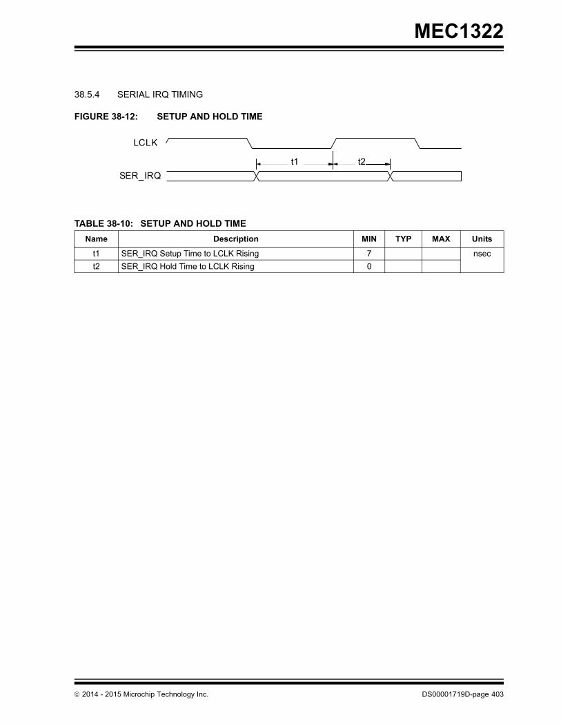
MEC1322
38.5.4 SERIAL IRQ TIMING
FIGURE 38-12: SETUP AND HOLD TIME
TABLE 38-10: SETUP AND HOLD TIME
Name Description MIN TYP MAX Units
t1 SER_IRQ Setup Time to LCLK Rising 7 nsec
t2 SER_IRQ Hold Time to LCLK Rising 0
t2 t1
LCLK
SER_IRQ
2014 - 2015 Microchip Technology Inc. DS00001719D-page 403

MEC1322
DS00001719D-page 404 2014 - 2015 Microchip Technology Inc.
38.6 Serial Port (UART) Data Timing
FIGURE 38-13: SERIAL PORT DATA
Note 38-8 tBR is 1/Baud Rate. The Baud Rate is programmed through the Baud_Rate_Divisor bits located inthe Programmable Baud Rate Generator registers. The selectable baud rates are listed in Table 14-7, "UART Baud Rates using Clock Source 1.8432MHz_Clk" and Table 14-8, "UART Baud Rates usingClock Source 24MHz_Clk". Some of the baud rates have some percentage of error because the clockdoes not divide evenly. This error can be determined from the values in these baud rate tables.
TABLE 38-11: SERIAL PORT DATA PARAMETERS
Name Description MIN TYP MAX Units
t1 Serial Port Data Bit Time tBR(Note 3
8-8)
nsec
Data (5-8 Bits)t1
Data
TXD1, 2Start Parity
Stop (1-2 Bits)

2014 - 2015 Microchip Technology Inc. DS00001719D-page 405
MEC1322
38.7 PECI Interface
Note 38-9 The originator must drive a more restrictive time to allow for quantized sampling errors by a clientyet still attain the minimum time less than 500 µsec. tBIT limits apply equally to tBIT-A and tBIT-M . TheMEC1322 is designed to support 2 MHz, or a 500ns bit time. See the PECI 3.0 specification fromIntel Corp. for further details.
Note 38-10 The minimum and maximum bit times are relative to tBIT defined in the Timing Negotiation pulse. Seethe PECI 3.0 specification from Intel Corp. for further details.
Note 38-11 “#nodes” is the number of nodes on the PECI bus; host and client nodes are counted as one each.Extended trace lengths may appear as extra nodes. Refer also to Table 23-2, "PECI RoutingGuidelines". See the PECI 3.0 specification from Intel Corp. for further details.
Table 1.1
Name Description MIN MAX Units Notes
tBIT Bit time (overall time evident on PECI pin) Bit time driven by an originator
0.4950.495
500250
µsecµsec
Note 38-9
tBIT,jitter Bit time jitter between adjacent bits in a PECI mes-sage header or data bytes after timing has been negotiated
- - %
tBIT,drift Change in bit time across a PECI address or PECI message bits as driven by the originator. This limit only applies across tBIT-A bit drift and tBIT-M drift.
- - %
tH1 High level time for logic 1 0.6 0.8 tBIT Note 38-10
tH0 High level time for logic 0 0.2 0.4 tBIT
tPECIR Rise time (measured from VOL to VIH,min , Vtt(nom)−5%)
- 30 + (5 x #nodes)
ns Note 38-11
tPECIF Fall time (measured from VOH to VIL,max , Vtt(nom)+5%)
- (30 x #nodes) ns Note 38-11

MEC1322
DS00001719D-page 406 2014 - 2015 Microchip Technology Inc.
38.8 8042 Emulation CPU_Reset Timing
FIGURE 38-14: CPU_RESET TIMING
Note 38-12 Figure 38-14 and Table 38-12 refer to FIGURE 11-5: CPU_RESET Implementation Diagram onpage 152 in which CPU_RESET is the inverse of ALT_RST# & KRESET.
Note 38-13 The KBRST pin function is the output of CPU_RESET described in Section 11.11.2, "CPU_RESETHardware Speed-Up," on page 151.
TABLE 38-12: CPU_RESET TIMING PARAMETERS
NAME DESCRIPTION MIN TYP MAX UNITS
tdelay Delay prior to active pulse 14 15 15.5 μs
tactive Active pulse width 6 8 8.5 μs
td e la y ta c t iv e

2014 - 2015 Microchip Technology Inc. DS00001719D-page 407
MEC1322
38.9 Keyboard Scan Matrix Timing
TABLE 38-13: ACTIVE PRE DRIVE MODE TIMING
Parameter SymbolValue
UnitsMIN TYP MAX
Active Predrive Mode tPREDRIVE 40.87 41.7 42.5 ns

MEC1322
38.10 PS/2 Timing
FIGURE 38-15: PS/2 TRANSMIT TIMING
TABLE 38-14: PS/2 CHANNEL TRANSMISSION TIMING PARAMETERS
Name Description MIN TYP MAX Units
t1 The PS/2 Channel’s CLK and DATA lines are floated following PS2_EN=1 and PS2_T/R=0.
1000 ns
t2 PS2_T/R bit set to CLK driven low prepar-ing the PS/2 Channel for data transmis-sion.
t3 CLK line floated to XMIT_IDLE bit de-asserted.
1.7
t4 Trailing edge of WR to Transmit Register to DATA line driven low.
45 90
t5 Trailing edge of EC WR of Transmit Regis-ter to CLK line floated.
90 130 ns
t6 Initiation of Start of Transmit cycle by the PS/2 channel controller to the auxiliary peripheral’s responding by latching the Start bit and driving the CLK line low.
0.002 25.003 ms
t7 Period of CLK 60 302 µs
t8 Duration of CLK high (active) 30 151
t9 Duration of CLK low (inactive)
t10 Duration of Data Frame. Falling edge of Start bit CLK (1st clk) to falling edge of Par-
ity bit CLK (10th clk).
2.002 ms
1 2 10 11
B0 B1 B2 B3 B4 B5 B6 B7 Ps
PS2_CLK
PS2_DAT
PS2_EN
PS2_T/R
XMIT_IDLE
RDATA_RDY
Write Tx Reg
Interrupt
t1
t2
t4
t3
t5 t6
t7
t9t8t10
t11
t12
t13
t14
t15
Note 1
t17
DS00001719D-page 408 2014 - 2015 Microchip Technology Inc.

MEC1322
t11 DATA output by MEC1322 following the falling edge of CLK. The auxiliary periph-eral device samples DATA following the ris-ing edge of CLK.
1.0 µs
t12 Rising edge following the 11th falling clock edge to PS_T/R bit driven low.
3.5 7.1 µs
t13 Trailing edge of PS_T/R to XMIT_IDLE bit asserted.
500 ns
t14 DATA released to high-Z following the PS2_T/R bit going low.
t15 XMIT_IDLE bit driven high to interrupt gen-erated. Note1- Interrupt is cleared by writing a 1 to the status bit in the GIRQ17 source regis-ter.
t17 Trailing edge of CLK is held low prior to going high-Z
FIGURE 38-16: PS/2 RECEIVE TIMING
TABLE 38-14: PS/2 CHANNEL TRANSMISSION TIMING PARAMETERS (CONTINUED)
Name Description MIN TYP MAX Units
t6
t5t4
t3
t2
t7
t1
t8 t9
t10
t12
t11
RDATA_RDY
Interrupt
PS2_EN
Read Rx Reg
D3D0 D2 D5D4 D6 D7 P SD1PS2_DATA
PS2_CLK
PS2_T/R
2014 - 2015 Microchip Technology Inc. DS00001719D-page 409

MEC1322
TABLE 38-15: PS/2 CHANNEL RECEIVE TIMING DIAGRAM PARAMETERS
Name Description MIN TYP MAX Units
t1 The PS/2 Channel’s CLK and DATA lines are floated following PS2_EN=1 and PS2_T/R=0.
1000 ns
t2 Period of CLK 60 302 µs
t3 Duration of CLK high (active) 30 151
t4 Duration of CLK low (inactive)
t5 DATA setup time to falling edge of CLK. MEC1322 samples the data line on the fall-ing CLK edge.
1
t6 DATA hold time from falling edge of CLK. MEC1322 samples the data line on the fall-ing CLK edge.
2
t7 Duration of Data Frame. Falling edge of Start bit CLK (1st clk) to falling edge of Par-ity bit CLK (10th clk).
2.002 ms
t8 Falling edge of 11th CLK to RDATA_RDY asserted.
1.6 µs
t9 Trailing edge of the EC’s RD signal of the Receive Register to RDATA_RDY bit de-asserted.
500 ns
t10 Trailing edge of the EC’s RD signal of the Receive Register to the CLK line released to high-Z.
t11 PS2_CLK is "Low" and PS2_DATA is "Hi-Z" when PS2_EN is de-asserted.
t12 RDATA_RDY asserted an interrupt is gen-erated.
DS00001719D-page 410 2014 - 2015 Microchip Technology Inc.

2014 - 2015 Microchip Technology Inc. DS00001719D-page 411
MEC1322
38.11 PWM Timing
FIGURE 38-17: PWM OUTPUT TIMING
TABLE 38-16: PWM TIMING PARAMETERS
Name Description MIN TYP MAX Units
t1 Period 42ns 23.3sec
tf Frequency 0.04Hz 24MHz
t2 High Time 0 11.65 sec
t3 Low Time 0 11.65 sec
td Duty cycle 0 100 %
t3t1
t2PWMx

MEC1322
DS00001719D-page 412 2014 - 2015 Microchip Technology Inc.
38.12 Fan Tachometer Timing
Note: tTACH is the clock used for the tachometer counter. It is 30.52 * prescaler, where the prescaler is pro-grammed in the Fan Tachometer Timebase Prescaler register.
FIGURE 38-18: FAN TACHOMETER INPUT TIMING
TABLE 38-17: FAN TACHOMETER INPUT TIMING PARAMETERS
Name Description MIN TYP MAX Units
t1 Pulse Time 100 µsec
t2 Pulse High Time 20
t3 Pulse Low Time 20
t3t1
t2FAN_TACHx
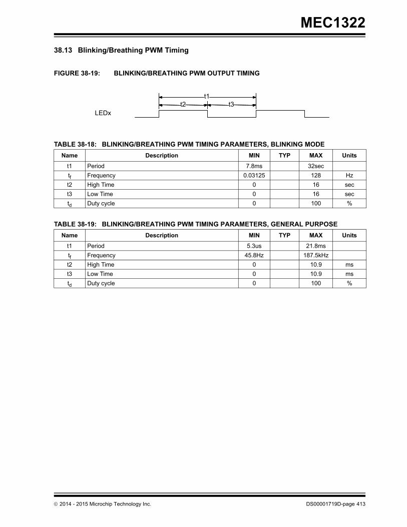
2014 - 2015 Microchip Technology Inc. DS00001719D-page 413
MEC1322
38.13 Blinking/Breathing PWM Timing
FIGURE 38-19: BLINKING/BREATHING PWM OUTPUT TIMING
TABLE 38-18: BLINKING/BREATHING PWM TIMING PARAMETERS, BLINKING MODE
Name Description MIN TYP MAX Units
t1 Period 7.8ms 32sec
tf Frequency 0.03125 128 Hz
t2 High Time 0 16 sec
t3 Low Time 0 16 sec
td Duty cycle 0 100 %
TABLE 38-19: BLINKING/BREATHING PWM TIMING PARAMETERS, GENERAL PURPOSE
Name Description MIN TYP MAX Units
t1 Period 5.3us 21.8ms
tf Frequency 45.8Hz 187.5kHz
t2 High Time 0 10.9 ms
t3 Low Time 0 10.9 ms
td Duty cycle 0 100 %
t3t1
t2LEDx

MEC1322
DS00001719D-page 414 2014 - 2015 Microchip Technology Inc.
38.14 I2C/SMBus Timing
FIGURE 38-20: I2C/SMBUS TIMING
TABLE 38-20: I2C/SMBUS TIMING PARAMETERS
Symbol Parameter
Standard-Mode
Fast-Mode
Fast-Mode Plus Units
MIN. MAX. MIN. MAX. MIN. MAX.
fSCL SCL Clock Frequency 100 400 1000 kHz
tBUF Bus Free Time 4.7 1.3 0.5 µs
tSU;STA START Condition Set-Up Time 4.7 0.6 0.26 µs
tHD;STA START Condition Hold Time 4.0 0.6 0.26 µs
tLOW SCL LOW Time 4.7 1.3 0.5 µs
tHIGH SCL HIGH Time 4.0 0.6 0.26 µs
tR SCL and SDA Rise Time 1.0 0.3 0.12 µs
tF SCL and SDA Fall Time 0.3 0.3 0.12 µs
tSU;DAT Data Set-Up Time 0.25 0.1 0.05 µs
tHD;DAT Data Hold Time 0 0 0 µs
tSU;STO STOP Condition Set-Up Time 4.0 0.6 0.26 µs
tHD;STA
tSU;STOtSU;STAtSU;DATtHIGH
tFtRtLOW
tHD;DAT
tHD;STA
tBUF
I2C_DATA
I2C_CLK

MEC1322
38.15 BC-Link Master Interrupt Timing
38.16 BC-Link Master Timing
FIGURE 38-21: BC-LINK ERR INTERRUPT TIMING
FIGURE 38-22: BC-LINK READ TIMING
BUSY
BC_ERR
BC_ERR Interrupt
BC_Busy_CLR Interrupt(Controlled by Hardware)
Approxinatley 48 BC Clocks
Bit n
tIH
Bit n-1BC_DAT
BC_CLK
tIS
tC
Bit Read
2014 - 2015 Microchip Technology Inc. DS00001719D-page 415

MEC1322
Note 1: The BC-Link Master DATA input (tIH in Table 38-21) must be stable before next rising edge of CLK.
2: The BC-Link Clock frequency is limited by the application usage model (see BC-Link Master Section 31.5,Signal Description). The BC-Link Clock frequency is controlled by the BC-Link Clock Select Register. Thetc(High Speed) parameter implies both BC-link master and companion devices are located on the same cir-cuit board and a high speed clock setting is possible.
FIGURE 38-23: BC-LINK WRITE TIMING
TABLE 38-21: BC-LINK MASTER TIMING DIAGRAM PARAMETERS
Name Description MIN TYP MAX Units
tc(High Speed) High Spec BC Clock Frequency 23.5 24 24.5 MHz
High Spec BC Clock Period 40.8 41.67 42.5 ns
tOS BC-Link Master DATA output setup time before rising edge of CLK.
tc-tOH-
MAX
nsec
tOH BC-Link Master Data hold time after falling edge of CLK
10 nsec
tIS BC-Link Master DATA input setup time before rising edge of CLK.
15 nsec
tIH BC-Link Master DATA input hold time after rising edge of CLK.
0 nsec
Note: The timing budget equation is as follows for data from BC-Link slave to master:
Tc > TOD(master-clk) + Tprop(clk) +TOD(slave) + Tprop(slave data) + TIS(master).
Bit nBit n-1
tC
tOH
tOS
BC_DAT
BC_CLK
DS00001719D-page 416 2014 - 2015 Microchip Technology Inc.

MEC1322
38.17 Serial Peripheral Interface (SPI) Timings
FIGURE 38-24: SPI CLOCK TIMING
Note 38-14 This timing value applies when the 48MHz ring oscillator is at its 48MHz operating frequency (with32 kHz present after frequency lock to 48MHz).
TABLE 38-22: SPI CLOCK TIMING PARAMETERS
NAME DESCRIPTION MIN TYP MAX UNITS
Tr SPI Clock Rise Time. Measured from 10% to 90%.
10% of SPCLK Period
ns
Tf SPI Clock Fall Time. Measured from 90% to 10%.
10% of SPCLK Period
ns
Th/Tl SPI Clock High Time/SPI Clock Low Time
40% of SPCLK Period
50% of SPCLK Period
60% of SPCLK Period
ns
Tp SPI Clock Period – As selected by SPI Clock Generator Register
20.8 (Note 38-14)
62492.25 ns
Tr Tf
Th Tl
Tp
SPICLK
2014 - 2015 Microchip Technology Inc. DS00001719D-page 417

MEC1322
FIGURE 38-25: SPI SETUP AND HOLD TIMES, CLKPOL=0, TCLKPH=0, RCLKPH=0
FIGURE 38-26: SPI SETUP AND HOLD TIMES, CLKPOL=0, TCLKPH=0, RCLKPH=1
38.17.1 SPI INTERFACE TIMINGS
The following timing diagrams represent a single-byte transfer over the SPI interface using different SPCLK phase set-tings. Data bits are transmitted in bit order starting with the MSB (LSBF=‘0’) or the LSB (LSBF=‘1’). See the SPI ControlRegister for information on the LSBF bit. The CS signal in each diagram is a generic bit-controlled chip select signalrequired by most peripheral devices. This signal and additional chip selects can be GPIO controlled. Note that thesetimings for Full Duplex Mode are also applicable to Half Duplex (or Bi-directional) mode.
TABLE 38-23: SPI SETUP AND HOLD TIMES PARAMETERS
NAME DESCRIPTION MIN TYP MAX UNITS
T1 Data Output Delay 5 ns
T2 Data IN Setup Time 10 ns
T3 Data IN Hold Time 0 ns
SPDIN
SPDOUT
T1
T2
T3
SPCLK(CLKPOL = 0, TCLKPH = 0, RCLKPH = 0)
Setup and Hold Times for Full-Duplex and Bidrectional Modes
SPDIN
SPDOUT
T1
T2
T3
SPCLK(CLKPOL = 0, TCLKPH = 0, RCLKPH = 1)
Setup and Hold Times for Full-Duplex and Bidrectional Modes
DS00001719D-page 418 2014 - 2015 Microchip Technology Inc.

MEC1322
FIGURE 38-27: INTERFACE TIMING, FULL DUPLEX MODE (TCLKPH = 0, RCLKPH = 0)
.
In this mode, data is available immediately when a device is selected and is sampled on the first and following oddSPCLK edges by the master and slave.
FIGURE 38-28: SPI INTERFACE TIMING, FULL DUPLEX MODE (TCLKPH = 1, RCLKPH = 0)
.
In this mode, the master requires an initial SPCLK edge before data is available. The data from slave is available imme-diately when the slave device is selected. The data is sampled on the first and following odd edges by the master. Thedata is sampled on the second and following even SPCLK edges by the slave.
SPCLK (CLKPOL = 0)
SPCLK (CLKPOL = 1)
SPDIN (RCLKPH = 0)
SPDOUT(TCLKPH = 0)
CS (GPIO)
LAST DATA BIT SAMPLED BY MASTER AND SLAVE
FIRST DATA BIT SAMPLED BY MASTER AND SLAVE
SPCLK (CLKPOL = 0)
SPCLK (CLKPOL = 1)
SPDOUT (TCLKPH = 1)
SPDIN(RCLKPH = 0)
CS (GPIO)
FIRST DATA BIT SAMPLED BY SLAVE
LAST DATA BIT SAMPLED BY SLAVE
FIRST DATA BIT SAMPLED BY MASTER
LAST DATA BIT SAMPLED BY MASTER
2014 - 2015 Microchip Technology Inc. DS00001719D-page 419

MEC1322
FIGURE 38-29: SPI INTERFACE TIMING, FULL DUPLEX MODE (TCLKPH = 0, RCLKPH = 1)
In this mode, the data from slave is available immediately when the slave device is selected. The slave device requiresan initial SPCLK edge before data is available. The data is sampled on the second and following even SPCLK edgesby the master. The data is sampled on the first and following odd edges by the slave.
FIGURE 38-30: SPI INTERFACE TIMING - FULL DUPLEX MODE (TCLKPH = 1, RCLKPH = 1)
In this mode, the master and slave require an initial SPCLK edge before data is available. Data is sampled on the secondand following even SPCLK edges by the master and slave.
SPCLK (CLKPOL = 0)
SPCLK (CLKPOL = 1)
SPDIN (RCLKPH = 1)
SPDOUT(TCLKPH = 0)
CS (GPIO)
FIRST DATA BIT SAMPLED BY MASTER
LAST DATA BIT SAMPLED BY MASTER
FIRST DATA BIT SAMPLED BY SLAVE
LAST DATA BIT SAMPLED BY SLAVE
SPCLK (CLKPOL = 0)
SPCLK (CLKPOL = 1)
SPDIN (RCLKPH = 1)
SPDOUT(TCLKPH = 1)
CS (GPIO)
FIRST DATA BIT SAMPLED BY MASTER AND SLAVE
LAST DATA BIT SAMPLED BY MASTER AND SLAVE
DS00001719D-page 420 2014 - 2015 Microchip Technology Inc.

2014 - 2015 Microchip Technology Inc. DS00001719D-page 421
MEC1322
38.18 Serial Debug Port Timing
FIGURE 38-31: SERIAL DEBUG PORT TIMING PARAMETERS
Note 38-15 When the clock divider for the embedded controller is an odd number value greater than 2h, thentCLK-L = tCLK-H + 15 ns. When the clock divider for the embedded controller is 0h, 1h, or an evennumber value greater than 2h, then tCLK-L = tCLK-H.
TABLE 38-24: SERIAL DEBUG PORT INTERFACE TIMING PARAMETERS
Name Description MIN TYP MAX Units
fclk TFDP Clock frequency (Note 38-15) 6 - 24 MHz
tP TFDP Clock Period. 1/fclk μs
tOD TFDP Data output delay after falling edge of MSCLK. 5 nsec
tOH TFDP Data hold time after falling edge of TFDP Clock tP - tOD nsec
tCLK-L TFDP Clock Low Time tP/2 - 3 tP/2 + 3 nsec
tCLK-H TFDP Clock high Time (see Note 38-15) tP/2 - 3 tP/2 + 3 nsec
tOD tOH
tP
tCLK-L tCLK-H
fCLK
TFDP Clock
TFDP Data

MEC1322
DS00001719D-page 422 2014 - 2015 Microchip Technology Inc.
38.19 JTAG Interface Timing
FIGURE 38-32: JTAG POWER-UP & ASYNCHRONOUS RESET TIMING
FIGURE 38-33: JTAG SETUP & HOLD PARAMETERS
TABLE 38-25: JTAG INTERFACE TIMING PARAMETERS
Name Description MIN TYP MAX Units
tsu JTAG_RST# de-assertion after VCC1 power is applied
5 ms
tpw JTAG_RST# assertion pulse width 500 nsec
fclk JTAG_CLK frequency (see note) 48 MHz
tOD TDO output delay after falling edge of TCLK. 5 10 nsec
tOH TDO hold time after falling edge of TCLK 1 TCLK - tOD nsec
tIS TDI setup time before rising edge of TCLK. 5 nsec
tIH TDI hold time after rising edge of TCLK. 5 nsec
Note: fclk is the maximum frequency to access a JTAG Register.
VCC1 Power
JTAG_RST#
tpw
fclk
tsu
2.8V
JTAG_CLK
JTAG _C LK
JTAG _TD O
JTAG _TD I
tO D
tIHtIS
tO H

MEC1322
39.0 MEMORY MAP
Address (Hex)
HW Block Instance Name
HW Block Instance No.
Reg. Bank Name Reg. Instance Name
0 32K ROM 0 32K ROM 32K ROM
100000 128K SRAM 0 128K SRAM 128K SRAM
40000400 Watchdog Timer Inter-face
0 WDT Registers WDT Load Register
40000404 Watchdog Timer Inter-face
0 WDT Registers WDT Control Register
40000408 Watchdog Timer Inter-face
0 WDT Registers WDT Kick Register
4000040C Watchdog Timer Inter-face
0 WDT Registers WDT Count Register
40000C00 Basic Timer 0 Basic_Timer_EC_Only Timer Count
40000C04 Basic Timer 0 Basic_Timer_EC_Only Timer Preload
40000C08 Basic Timer 0 Basic_Timer_EC_Only Timer Status
40000C0C Basic Timer 0 Basic_Timer_EC_Only Timer Interrupt Enable
40000C10 Basic Timer 0 Basic_Timer_EC_Only Timer Control
40000C20 Basic Timer 1 Basic_Timer_EC_Only Timer Count
40000C24 Basic Timer 1 Basic_Timer_EC_Only Timer Preload
40000C28 Basic Timer 1 Basic_Timer_EC_Only Timer Status
40000C2C Basic Timer 1 Basic_Timer_EC_Only Timer Interrupt Enable
40000C30 Basic Timer 1 Basic_Timer_EC_Only Timer Control
40000C40 Basic Timer 2 Basic_Timer_EC_Only Timer Count
40000C44 Basic Timer 2 Basic_Timer_EC_Only Timer Preload
40000C48 Basic Timer 2 Basic_Timer_EC_Only Timer Status
40000C4C Basic Timer 2 Basic_Timer_EC_Only Timer Interrupt Enable
40000C50 Basic Timer 2 Basic_Timer_EC_Only Timer Control
40000C60 Basic Timer 3 Basic_Timer_EC_Only Timer Count
40000C64 Basic Timer 3 Basic_Timer_EC_Only Timer Preload
40000C68 Basic Timer 3 Basic_Timer_EC_Only Timer Status
40000C6C Basic Timer 3 Basic_Timer_EC_Only Timer Interrupt Enable
40000C70 Basic Timer 3 Basic_Timer_EC_Only Timer Control
40000C80 Basic Timer 4 Basic_Timer_EC_Only Timer Count
40000C84 Basic Timer 4 Basic_Timer_EC_Only Timer Preload
40000C88 Basic Timer 4 Basic_Timer_EC_Only Timer Status
40000C8C Basic Timer 4 Basic_Timer_EC_Only Timer Interrupt Enable
40000C90 Basic Timer 4 Basic_Timer_EC_Only Timer Control
40000CA0 Basic Timer 5 Basic_Timer_EC_Only Timer Count
40000CA4 Basic Timer 5 Basic_Timer_EC_Only Timer Preload
40000CA8 Basic Timer 5 Basic_Timer_EC_Only Timer Status
40000CAC Basic Timer 5 Basic_Timer_EC_Only Timer Interrupt Enable
40000CB0 Basic Timer 5 Basic_Timer_EC_Only Timer Control
40001800 SMB Device Interface 0 SMB_EC_Only Status Register
40001800 SMB Device Interface 0 SMB_EC_Only Control Register
2014 - 2015 Microchip Technology Inc. DS00001719D-page 423

MEC1322
40001801 SMB Device Interface 0 SMB_EC_Only Reserved
40001804 SMB Device Interface 0 SMB_EC_Only Own Address Register
40001806 SMB Device Interface 0 SMB_EC_Only Reserved
40001808 SMB Device Interface 0 SMB_EC_Only Data
40001809 SMB Device Interface 0 SMB_EC_Only Reserved
4000180C SMB Device Interface 0 SMB_EC_Only SMBus Master Command Register
40001810 SMB Device Interface 0 SMB_EC_Only SMBus Slave Command Register
40001814 SMB Device Interface 0 SMB_EC_Only PEC Register
40001815 SMB Device Interface 0 SMB_EC_Only Reserved
40001818 SMB Device Interface 0 SMB_EC_Only DATA_TIMING2
40001819 SMB Device Interface 0 SMB_EC_Only Reserved
40001820 SMB Device Interface 0 SMB_EC_Only Completion Register
40001824 SMB Device Interface 0 SMB_EC_Only Idle Scaling Register
40001828 SMB Device Interface 0 SMB_EC_Only Configuration Register
4000182C SMB Device Interface 0 SMB_EC_Only Bus Clock Register
4000182E SMB Device Interface 0 SMB_EC_Only Reserved
40001830 SMB Device Interface 0 SMB_EC_Only Block ID Register
40001831 SMB Device Interface 0 SMB_EC_Only Reserved
40001834 SMB Device Interface 0 SMB_EC_Only Revision Register
40001835 SMB Device Interface 0 SMB_EC_Only Reserved
40001838 SMB Device Interface 0 SMB_EC_Only Bit-Bang Control Register
40001839 SMB Device Interface 0 SMB_EC_Only Reserved
4000183C SMB Device Interface 0 SMB_EC_Only Clock Sync
40001840 SMB Device Interface 0 SMB_EC_Only Data Timing Register
40001844 SMB Device Interface 0 SMB_EC_Only Time-Out Scaling Register
40001848 SMB Device Interface 0 SMB_EC_Only SMBus Slave Transmit Buffer Register
40001849 SMB Device Interface 0 SMB_EC_Only Reserved
4000184C SMB Device Interface 0 SMB_EC_Only SMBus Slave Receive Buf-fer Register
4000184D SMB Device Interface 0 SMB_EC_Only Reserved
40001850 SMB Device Interface 0 SMB_EC_Only SMBus Master Transmit Bufer Register
40001851 SMB Device Interface 0 SMB_EC_Only Reserved
40001854 SMB Device Interface 0 SMB_EC_Only SMBus Master Receive Buffer Register
40001855 SMB Device Interface 0 SMB_EC_Only Reserved
40002400 DMA 0 DMA Main DMA Main Control Register
40002401 DMA 0 DMA Main DMA Reserved
40002404 DMA 0 DMA Main DMA Data Register
40002410 DMA 0 DMA_CH0 DMA Activate Register
40002414 DMA 0 DMA_CH0 DMA Memory Start Address Register
Address (Hex)
HW Block Instance Name
HW Block Instance No.
Reg. Bank Name Reg. Instance Name
DS00001719D-page 424 2014 - 2015 Microchip Technology Inc.

MEC1322
40002418 DMA 0 DMA_CH0 DMA Memory End Address Register
4000241C DMA 0 DMA_CH0 AHB Address Register
40002420 DMA 0 DMA_CH0 DMA Control Register
40002424 DMA 0 DMA_CH0 DMA Channel Interrupt Status
40002428 DMA 0 DMA_CH0 DMA Channel Interrupt Enable
4000242C DMA 0 DMA_CH0 DMA Test Register
40002430 DMA 0 DMA_CH1 DMA Activate Register
40002434 DMA 0 DMA_CH1 DMA Memory Start Address Register
40002438 DMA 0 DMA_CH1 DMA Memory End Address Register
4000243C DMA 0 DMA_CH1 AHB Address Register
40002440 DMA 0 DMA_CH1 DMA Control Register
40002444 DMA 0 DMA_CH1 DMA Channel Interrupt Status
40002448 DMA 0 DMA_CH1 DMA Channel Interrupt Enable
4000244C DMA 0 DMA_CH1 DMA Test Register
40002450 DMA 0 DMA_CH2 DMA Activate Register
40002454 DMA 0 DMA_CH2 DMA Memory Start Address Register
40002458 DMA 0 DMA_CH2 DMA Memory End Address Register
4000245C DMA 0 DMA_CH2 AHB Address Register
40002460 DMA 0 DMA_CH2 DMA Control Register
40002464 DMA 0 DMA_CH2 DMA Channel Interrupt Status
40002468 DMA 0 DMA_CH2 DMA Channel Interrupt Enable
4000246C DMA 0 DMA_CH2 DMA Test Register
40002470 DMA 0 DMA_CH3 DMA Activate Register
40002474 DMA 0 DMA_CH3 DMA Memory Start Address Register
40002478 DMA 0 DMA_CH3 DMA Memory End Address Register
4000247C DMA 0 DMA_CH3 AHB Address Register
40002480 DMA 0 DMA_CH3 DMA Control Register
40002484 DMA 0 DMA_CH3 DMA Channel Interrupt Status
40002488 DMA 0 DMA_CH3 DMA Channel Interrupt Enable
4000248C DMA 0 DMA_CH3 DMA Test Register
40002490 DMA 0 DMA_CH4 DMA Activate Register
Address (Hex)
HW Block Instance Name
HW Block Instance No.
Reg. Bank Name Reg. Instance Name
2014 - 2015 Microchip Technology Inc. DS00001719D-page 425

MEC1322
40002494 DMA 0 DMA_CH4 DMA Memory Start Address Register
40002498 DMA 0 DMA_CH4 DMA Memory End Address Register
4000249C DMA 0 DMA_CH4 AHB Address Register
400024A0 DMA 0 DMA_CH4 DMA Control Register
400024A4 DMA 0 DMA_CH4 DMA Channel Interrupt Status
400024A8 DMA 0 DMA_CH4 DMA Channel Interrupt Enable
400024AC DMA 0 DMA_CH4 DMA Test Register
400024B0 DMA 0 DMA_CH5 DMA Activate Register
400024B4 DMA 0 DMA_CH5 DMA Memory Start Address Register
400024B8 DMA 0 DMA_CH5 DMA Memory End Address Register
400024BC DMA 0 DMA_CH5 AHB Address Register
400024C0 DMA 0 DMA_CH5 DMA Control Register
400024C4 DMA 0 DMA_CH5 DMA Channel Interrupt Status
400024C8 DMA 0 DMA_CH5 DMA Channel Interrupt Enable
400024CC DMA 0 DMA_CH5 DMA Test Register
400024D0 DMA 0 DMA_CH6 DMA Activate Register
400024D4 DMA 0 DMA_CH6 DMA Memory Start Address Register
400024D8 DMA 0 DMA_CH6 DMA Memory End Address Register
400024DC DMA 0 DMA_CH6 AHB Address Register
400024E0 DMA 0 DMA_CH6 DMA Control Register
400024E4 DMA 0 DMA_CH6 DMA Channel Interrupt Status
400024E8 DMA 0 DMA_CH6 DMA Channel Interrupt Enable
400024EC DMA 0 DMA_CH6 DMA Test Register
400024F0 DMA 0 DMA_CH7 DMA Activate Register
400024F4 DMA 0 DMA_CH7 DMA Memory Start Address Register
400024F8 DMA 0 DMA_CH7 DMA Memory End Address Register
400024FC DMA 0 DMA_CH7 AHB Address Register
40002500 DMA 0 DMA_CH7 DMA Control Register
40002504 DMA 0 DMA_CH7 DMA Channel Interrupt Status
40002508 DMA 0 DMA_CH7 DMA Channel Interrupt Enable
4000250C DMA 0 DMA_CH7 DMA Test Register
Address (Hex)
HW Block Instance Name
HW Block Instance No.
Reg. Bank Name Reg. Instance Name
DS00001719D-page 426 2014 - 2015 Microchip Technology Inc.
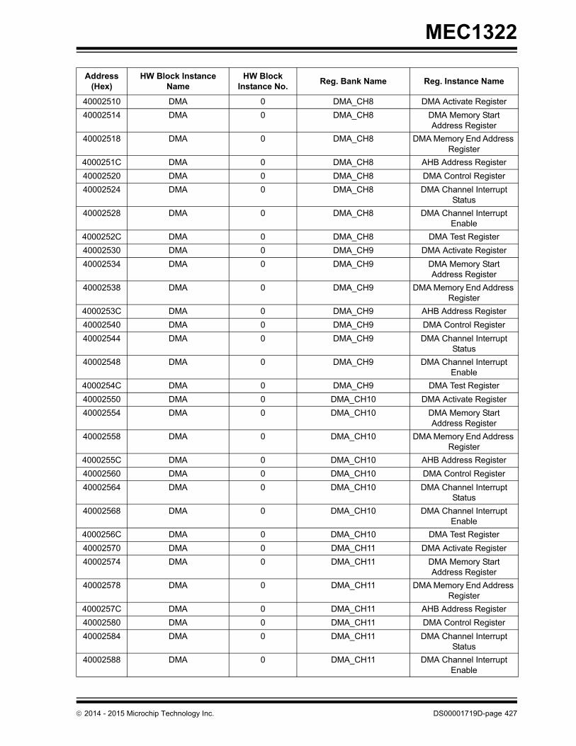
MEC1322
40002510 DMA 0 DMA_CH8 DMA Activate Register
40002514 DMA 0 DMA_CH8 DMA Memory Start Address Register
40002518 DMA 0 DMA_CH8 DMA Memory End Address Register
4000251C DMA 0 DMA_CH8 AHB Address Register
40002520 DMA 0 DMA_CH8 DMA Control Register
40002524 DMA 0 DMA_CH8 DMA Channel Interrupt Status
40002528 DMA 0 DMA_CH8 DMA Channel Interrupt Enable
4000252C DMA 0 DMA_CH8 DMA Test Register
40002530 DMA 0 DMA_CH9 DMA Activate Register
40002534 DMA 0 DMA_CH9 DMA Memory Start Address Register
40002538 DMA 0 DMA_CH9 DMA Memory End Address Register
4000253C DMA 0 DMA_CH9 AHB Address Register
40002540 DMA 0 DMA_CH9 DMA Control Register
40002544 DMA 0 DMA_CH9 DMA Channel Interrupt Status
40002548 DMA 0 DMA_CH9 DMA Channel Interrupt Enable
4000254C DMA 0 DMA_CH9 DMA Test Register
40002550 DMA 0 DMA_CH10 DMA Activate Register
40002554 DMA 0 DMA_CH10 DMA Memory Start Address Register
40002558 DMA 0 DMA_CH10 DMA Memory End Address Register
4000255C DMA 0 DMA_CH10 AHB Address Register
40002560 DMA 0 DMA_CH10 DMA Control Register
40002564 DMA 0 DMA_CH10 DMA Channel Interrupt Status
40002568 DMA 0 DMA_CH10 DMA Channel Interrupt Enable
4000256C DMA 0 DMA_CH10 DMA Test Register
40002570 DMA 0 DMA_CH11 DMA Activate Register
40002574 DMA 0 DMA_CH11 DMA Memory Start Address Register
40002578 DMA 0 DMA_CH11 DMA Memory End Address Register
4000257C DMA 0 DMA_CH11 AHB Address Register
40002580 DMA 0 DMA_CH11 DMA Control Register
40002584 DMA 0 DMA_CH11 DMA Channel Interrupt Status
40002588 DMA 0 DMA_CH11 DMA Channel Interrupt Enable
Address (Hex)
HW Block Instance Name
HW Block Instance No.
Reg. Bank Name Reg. Instance Name
2014 - 2015 Microchip Technology Inc. DS00001719D-page 427

MEC1322
4000258C DMA 0 DMA_CH11 DMA Test Register
40005800 PWM 0 PWM_EC_Only PWM Counter ON Time Register
40005804 PWM 0 PWM_EC_Only PWM Counter OFF Time Register
40005808 PWM 0 PWM_EC_Only PWM Configuration Regis-ter
4000580C PWM 0 PWM_EC_Only Reserved
40005810 PWM 1 PWM_EC_Only PWM Counter ON Time Register
40005814 PWM 1 PWM_EC_Only PWM Counter OFF Time Register
40005818 PWM 1 PWM_EC_Only PWM Configuration Regis-ter
4000581C PWM 1 PWM_EC_Only Reserved
40005820 PWM 2 PWM_EC_Only PWM Counter ON Time Register
40005824 PWM 2 PWM_EC_Only PWM Counter OFF Time Register
40005828 PWM 2 PWM_EC_Only PWM Configuration Regis-ter
4000582C PWM 2 PWM_EC_Only Reserved
40005830 PWM 3 PWM_EC_Only PWM Counter ON Time Register
40005834 PWM 3 PWM_EC_Only PWM Counter OFF Time Register
40005838 PWM 3 PWM_EC_Only PWM Configuration Regis-ter
4000583C PWM 3 PWM_EC_Only Reserved
40006000 TACH 0 TACH_EC_ONLY TACH Control Register
40006004 TACH 0 TACH_EC_ONLY TACH Status Register
40006008 TACH 0 TACH_EC_ONLY TACH High Limit Register
4000600C TACH 0 TACH_EC_ONLY TACH Low Limit Register
40006010 TACH 1 TACH_EC_ONLY TACH Control Register
40006014 TACH 1 TACH_EC_ONLY TACH Status Register
40006018 TACH 1 TACH_EC_ONLY TACH High Limit Register
4000601C TACH 1 TACH_EC_ONLY TACH Low Limit Register
40006400 PECI 0 PECI_EC_Only PECI Write Data Register
40006404 PECI 0 PECI_EC_Only PECI Read Data Register
40006408 PECI 0 PECI_EC_Only PECI Control Register
4000640C PECI 0 PECI_EC_Only PECI Status 1 Register
40006410 PECI 0 PECI_EC_Only PECI Status 2 Register
40006414 PECI 0 PECI_EC_Only PECI Error Register
40006418 PECI 0 PECI_EC_Only PECI Interrupt Enable 1 Register
4000641C PECI 0 PECI_EC_Only PECI Interrupt Enable 2 Register
Address (Hex)
HW Block Instance Name
HW Block Instance No.
Reg. Bank Name Reg. Instance Name
DS00001719D-page 428 2014 - 2015 Microchip Technology Inc.

MEC1322
40006420 PECI 0 PECI_EC_Only PECI Optimal Bit Time (Low Byte) Register
40006424 PECI 0 PECI_EC_Only PECI Optimal Bit Time (High Byte) Register
40006428 PECI 0 PECI_EC_Only PECI Request Timer (Low Byte) Register
4000642C PECI 0 PECI_EC_Only PECI Request Timer (High Byte) Register
40006430 PECI 0 PECI_EC_Only PECI Reserved
40006440 PECI 0 PECI_EC_Only PECI Block ID Register
40006444 PECI 0 PECI_EC_Only Block Revision
40007C00 ADC 0 ADC Registers ADC Control Register
40007C04 ADC 0 ADC Registers ADC Delay Register
40007C08 ADC 0 ADC Registers ADC Status Register
40007C0C ADC 0 ADC Registers ADC Single Register
40007C10 ADC 0 ADC Registers ADC Repeat Register
40007C14 ADC 0 ADC Registers ADC Channel 0 Reading Registers
40007C18 ADC 0 ADC Registers ADC Channel 1 Reading Registers
40007C1C ADC 0 ADC Registers ADC Channel 2 Reading Registers
40007C20 ADC 0 ADC Registers ADC Channel 3 Reading Registers
40007C24 ADC 0 ADC Registers ADC Channel 4 Reading Registers
40007C54 ADC 0 ADC Registers ADC Test Register
40007C58 ADC 0 ADC Registers ADC Test Register
40007C78 ADC 0 ADC Registers ADC Test Register
40007C7C ADC 0 ADC Registers ADC Configuration Regis-ter
40008C00 Trace FIFO Debug Port 0 TFDP Data
40008C04 Trace FIFO Debug Port 0 TFDP Control
40009000 PS/2 0 Registers PS/2 Transmit Buffer Reg-ister
40009000 PS/2 0 Registers PS/2 Receive Buffer Regis-ter
40009004 PS/2 0 Registers PS/2 Control Register
40009008 PS/2 0 Registers PS/2 Status Register
40009040 PS/2 1 Registers PS/2 Transmit Buffer Reg-ister
40009040 PS/2 1 Registers PS/2 Receive Buffer Regis-ter
40009044 PS/2 1 Registers PS/2 Control Register
40009048 PS/2 1 Registers PS/2 Status Register
40009080 PS/2 2 Registers PS/2 Receive Buffer Regis-ter
Address (Hex)
HW Block Instance Name
HW Block Instance No.
Reg. Bank Name Reg. Instance Name
2014 - 2015 Microchip Technology Inc. DS00001719D-page 429

MEC1322
40009080 PS/2 2 Registers PS/2 Transmit Buffer Reg-ister
40009084 PS/2 2 Registers PS/2 Control Register
40009088 PS/2 2 Registers PS/2 Status Register
400090C0 PS/2 3 Registers PS/2 Transmit Buffer Reg-ister
400090C0 PS/2 3 Registers PS/2 Receive Buffer Regis-ter
400090C4 PS/2 3 Registers PS/2 Control Register
400090C8 PS/2 3 Registers PS/2 Status Register
40009400 EC GP-SPI 0 GP-SPI_EC_Only SPI Enable Register
40009404 EC GP-SPI 0 GP-SPI_EC_Only SPI Control Register
40009408 EC GP-SPI 0 GP-SPI_EC_Only SPI Status Register
4000940C EC GP-SPI 0 GP-SPI_EC_Only SPI TX_Data Register
40009410 EC GP-SPI 0 GP-SPI_EC_Only SPI RX_Data Register
40009414 EC GP-SPI 0 GP-SPI_EC_Only SPI Clock Control Register
40009418 EC GP-SPI 0 GP-SPI_EC_Only SPI Clock Generator Reg-ister
40009480 EC GP-SPI 1 GP-SPI_EC_Only SPI Enable Register
40009484 EC GP-SPI 1 GP-SPI_EC_Only SPI Control Register
40009488 EC GP-SPI 1 GP-SPI_EC_Only SPI Status Register
4000948C EC GP-SPI 1 GP-SPI_EC_Only SPI TX_Data Register
40009490 EC GP-SPI 1 GP-SPI_EC_Only SPI RX_Data Register
40009494 EC GP-SPI 1 GP-SPI_EC_Only SPI Clock Control Register
40009498 EC GP-SPI 1 GP-SPI_EC_Only SPI Clock Generator Reg-ister
40009800 Hibernation Timer 0 Registers HTimer x Preload Register
40009804 Hibernation Timer 0 Registers Hibernation Timer x Control Register
40009808 Hibernation Timer 0 Registers Hibernation Timer x Count Register
40009C00 Keyboard Matrix Scan Support
0 Registers Reserved
40009C04 Keyboard Matrix Scan Support
0 Registers KSO Select Register
40009C08 Keyboard Matrix Scan Support
0 Registers KSI Input Register
40009C0C Keyboard Matrix Scan Support
0 Registers KSI Status Register
40009C10 Keyboard Matrix Scan Support
0 Registers KSI Interrupt Enable Regis-ter
40009C14 Keyboard Matrix Scan Support
0 Registers Keyscan Extended Control Register
4000A000 RPM Fan Control 0 RPM_FAN Fan Setting
4000A001 RPM Fan Control 0 RPM_FAN PWM Divide
4000A002 RPM Fan Control 0 RPM_FAN Fan Configuration 1
Address (Hex)
HW Block Instance Name
HW Block Instance No.
Reg. Bank Name Reg. Instance Name
DS00001719D-page 430 2014 - 2015 Microchip Technology Inc.

MEC1322
4000A003 RPM Fan Control 0 RPM_FAN Fan Configuration 2
4000A004 RPM Fan Control 0 RPM_FAN MCHP Reserved
4000A005 RPM Fan Control 0 RPM_FAN Gain
4000A006 RPM Fan Control 0 RPM_FAN Fan Spin Up Configuration
4000A007 RPM Fan Control 0 RPM_FAN Fan Step
4000A008 RPM Fan Control 0 RPM_FAN Fan Minimum Drive
4000A009 RPM Fan Control 0 RPM_FAN Valid Tach Count
4000A00A RPM Fan Control 0 RPM_FAN Fan Drive Fail Band Low Byte
4000A00B RPM Fan Control 0 RPM_FAN Fan Drive Fail Band High Byte
4000A00C RPM Fan Control 0 RPM_FAN Tach Target Low Byte
4000A00D RPM Fan Control 0 RPM_FAN Tach Target High Byte
4000A00E RPM Fan Control 0 RPM_FAN Tach Reading Low Byte
4000A00F RPM Fan Control 0 RPM_FAN Tach Reading High Byte
4000A010 RPM Fan Control 0 RPM_FAN PWM Driver Base Fre-quency
4000A011 RPM Fan Control 0 RPM_FAN Fan Status
4000A012 RPM Fan Control 0 RPM_FAN Reserved
4000A014 RPM Fan Control 0 RPM_FAN RPM Fan Test
4000A015 RPM Fan Control 0 RPM_FAN RPM Fan Test1
4000A016 RPM Fan Control 0 RPM_FAN RPM Fan Test2
4000A017 RPM Fan Control 0 RPM_FAN RPM Fan Test3
4000A400 VBAT Registers 0 VBAT_EC_REG_BANK Power-Fail and Reset Sta-tus Register
4000A404 VBAT Registers 0 VBAT_EC_REG_BANK Control
4000A800 VBAT Powered RAM 0 Registers VBAT Backed Memory
4000AC00 SMB Device Interface 1 SMB_EC_Only Control Register
4000AC00 SMB Device Interface 1 SMB_EC_Only Status Register
4000AC01 SMB Device Interface 1 SMB_EC_Only Reserved
4000AC04 SMB Device Interface 1 SMB_EC_Only Own Address Register
4000AC06 SMB Device Interface 1 SMB_EC_Only Reserved
4000AC08 SMB Device Interface 1 SMB_EC_Only Data
4000AC09 SMB Device Interface 1 SMB_EC_Only Reserved
4000AC0C SMB Device Interface 1 SMB_EC_Only SMBus Master Command Register
4000AC10 SMB Device Interface 1 SMB_EC_Only SMBus Slave Command Register
4000AC14 SMB Device Interface 1 SMB_EC_Only PEC Register
4000AC15 SMB Device Interface 1 SMB_EC_Only Reserved
4000AC18 SMB Device Interface 1 SMB_EC_Only DATA_TIMING2
4000AC19 SMB Device Interface 1 SMB_EC_Only Reserved
4000AC20 SMB Device Interface 1 SMB_EC_Only Completion Register
4000AC24 SMB Device Interface 1 SMB_EC_Only Idle Scaling Register
Address (Hex)
HW Block Instance Name
HW Block Instance No.
Reg. Bank Name Reg. Instance Name
2014 - 2015 Microchip Technology Inc. DS00001719D-page 431

MEC1322
4000AC28 SMB Device Interface 1 SMB_EC_Only Configuration Register
4000AC2C SMB Device Interface 1 SMB_EC_Only Bus Clock Register
4000AC2E SMB Device Interface 1 SMB_EC_Only Reserved
4000AC30 SMB Device Interface 1 SMB_EC_Only Block ID Register
4000AC31 SMB Device Interface 1 SMB_EC_Only Reserved
4000AC34 SMB Device Interface 1 SMB_EC_Only Revision Register
4000AC35 SMB Device Interface 1 SMB_EC_Only Reserved
4000AC38 SMB Device Interface 1 SMB_EC_Only Bit-Bang Control Register
4000AC39 SMB Device Interface 1 SMB_EC_Only Reserved
4000AC3C SMB Device Interface 1 SMB_EC_Only Clock Sync
4000AC40 SMB Device Interface 1 SMB_EC_Only Data Timing Register
4000AC44 SMB Device Interface 1 SMB_EC_Only Time-Out Scaling Register
4000AC48 SMB Device Interface 1 SMB_EC_Only SMBus Slave Transmit Buffer Register
4000AC49 SMB Device Interface 1 SMB_EC_Only Reserved
4000AC4C SMB Device Interface 1 SMB_EC_Only SMBus Slave Receive Buf-fer Register
4000AC4D SMB Device Interface 1 SMB_EC_Only Reserved
4000AC50 SMB Device Interface 1 SMB_EC_Only SMBus Master Transmit Bufer Register
4000AC51 SMB Device Interface 1 SMB_EC_Only Reserved
4000AC54 SMB Device Interface 1 SMB_EC_Only SMBus Master Receive Buffer Register
4000AC55 SMB Device Interface 1 SMB_EC_Only Reserved
4000B000 SMB Device Interface 2 SMB_EC_Only Control Register
4000B000 SMB Device Interface 2 SMB_EC_Only Status Register
4000B001 SMB Device Interface 2 SMB_EC_Only Reserved
4000B004 SMB Device Interface 2 SMB_EC_Only Own Address Register
4000B006 SMB Device Interface 2 SMB_EC_Only Reserved
4000B008 SMB Device Interface 2 SMB_EC_Only Data
4000B009 SMB Device Interface 2 SMB_EC_Only Reserved
4000B00C SMB Device Interface 2 SMB_EC_Only SMBus Master Command Register
4000B010 SMB Device Interface 2 SMB_EC_Only SMBus Slave Command Register
4000B014 SMB Device Interface 2 SMB_EC_Only PEC Register
4000B015 SMB Device Interface 2 SMB_EC_Only Reserved
4000B018 SMB Device Interface 2 SMB_EC_Only DATA_TIMING2
4000B019 SMB Device Interface 2 SMB_EC_Only Reserved
4000B020 SMB Device Interface 2 SMB_EC_Only Completion Register
4000B024 SMB Device Interface 2 SMB_EC_Only Idle Scaling Register
4000B028 SMB Device Interface 2 SMB_EC_Only Configuration Register
4000B02C SMB Device Interface 2 SMB_EC_Only Bus Clock Register
4000B02E SMB Device Interface 2 SMB_EC_Only Reserved
Address (Hex)
HW Block Instance Name
HW Block Instance No.
Reg. Bank Name Reg. Instance Name
DS00001719D-page 432 2014 - 2015 Microchip Technology Inc.

MEC1322
4000B030 SMB Device Interface 2 SMB_EC_Only Block ID Register
4000B031 SMB Device Interface 2 SMB_EC_Only Reserved
4000B034 SMB Device Interface 2 SMB_EC_Only Revision Register
4000B035 SMB Device Interface 2 SMB_EC_Only Reserved
4000B038 SMB Device Interface 2 SMB_EC_Only Bit-Bang Control Register
4000B039 SMB Device Interface 2 SMB_EC_Only Reserved
4000B03C SMB Device Interface 2 SMB_EC_Only Clock Sync
4000B040 SMB Device Interface 2 SMB_EC_Only Data Timing Register
4000B044 SMB Device Interface 2 SMB_EC_Only Time-Out Scaling Register
4000B048 SMB Device Interface 2 SMB_EC_Only SMBus Slave Transmit Buffer Register
4000B049 SMB Device Interface 2 SMB_EC_Only Reserved
4000B04C SMB Device Interface 2 SMB_EC_Only SMBus Slave Receive Buf-fer Register
4000B04D SMB Device Interface 2 SMB_EC_Only Reserved
4000B050 SMB Device Interface 2 SMB_EC_Only SMBus Master Transmit Bufer Register
4000B051 SMB Device Interface 2 SMB_EC_Only Reserved
4000B054 SMB Device Interface 2 SMB_EC_Only SMBus Master Receive Buffer Register
4000B055 SMB Device Interface 2 SMB_EC_Only Reserved
4000B400 SMB Device Interface 3 SMB_EC_Only Control Register
4000B400 SMB Device Interface 3 SMB_EC_Only Status Register
4000B401 SMB Device Interface 3 SMB_EC_Only Reserved
4000B404 SMB Device Interface 3 SMB_EC_Only Own Address Register
4000B406 SMB Device Interface 3 SMB_EC_Only Reserved
4000B408 SMB Device Interface 3 SMB_EC_Only Data
4000B409 SMB Device Interface 3 SMB_EC_Only Reserved
4000B40C SMB Device Interface 3 SMB_EC_Only SMBus Master Command Register
4000B410 SMB Device Interface 3 SMB_EC_Only SMBus Slave Command Register
4000B414 SMB Device Interface 3 SMB_EC_Only PEC Register
4000B415 SMB Device Interface 3 SMB_EC_Only Reserved
4000B418 SMB Device Interface 3 SMB_EC_Only DATA_TIMING2
4000B419 SMB Device Interface 3 SMB_EC_Only Reserved
4000B420 SMB Device Interface 3 SMB_EC_Only Completion Register
4000B424 SMB Device Interface 3 SMB_EC_Only Idle Scaling Register
4000B428 SMB Device Interface 3 SMB_EC_Only Configuration Register
4000B42C SMB Device Interface 3 SMB_EC_Only Bus Clock Register
4000B42E SMB Device Interface 3 SMB_EC_Only Reserved
4000B430 SMB Device Interface 3 SMB_EC_Only Block ID Register
4000B431 SMB Device Interface 3 SMB_EC_Only Reserved
4000B434 SMB Device Interface 3 SMB_EC_Only Revision Register
Address (Hex)
HW Block Instance Name
HW Block Instance No.
Reg. Bank Name Reg. Instance Name
2014 - 2015 Microchip Technology Inc. DS00001719D-page 433
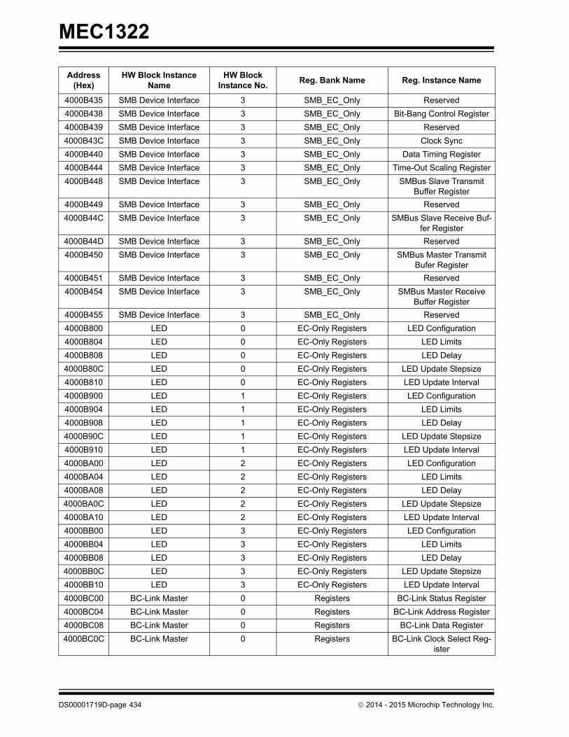
MEC1322
4000B435 SMB Device Interface 3 SMB_EC_Only Reserved
4000B438 SMB Device Interface 3 SMB_EC_Only Bit-Bang Control Register
4000B439 SMB Device Interface 3 SMB_EC_Only Reserved
4000B43C SMB Device Interface 3 SMB_EC_Only Clock Sync
4000B440 SMB Device Interface 3 SMB_EC_Only Data Timing Register
4000B444 SMB Device Interface 3 SMB_EC_Only Time-Out Scaling Register
4000B448 SMB Device Interface 3 SMB_EC_Only SMBus Slave Transmit Buffer Register
4000B449 SMB Device Interface 3 SMB_EC_Only Reserved
4000B44C SMB Device Interface 3 SMB_EC_Only SMBus Slave Receive Buf-fer Register
4000B44D SMB Device Interface 3 SMB_EC_Only Reserved
4000B450 SMB Device Interface 3 SMB_EC_Only SMBus Master Transmit Bufer Register
4000B451 SMB Device Interface 3 SMB_EC_Only Reserved
4000B454 SMB Device Interface 3 SMB_EC_Only SMBus Master Receive Buffer Register
4000B455 SMB Device Interface 3 SMB_EC_Only Reserved
4000B800 LED 0 EC-Only Registers LED Configuration
4000B804 LED 0 EC-Only Registers LED Limits
4000B808 LED 0 EC-Only Registers LED Delay
4000B80C LED 0 EC-Only Registers LED Update Stepsize
4000B810 LED 0 EC-Only Registers LED Update Interval
4000B900 LED 1 EC-Only Registers LED Configuration
4000B904 LED 1 EC-Only Registers LED Limits
4000B908 LED 1 EC-Only Registers LED Delay
4000B90C LED 1 EC-Only Registers LED Update Stepsize
4000B910 LED 1 EC-Only Registers LED Update Interval
4000BA00 LED 2 EC-Only Registers LED Configuration
4000BA04 LED 2 EC-Only Registers LED Limits
4000BA08 LED 2 EC-Only Registers LED Delay
4000BA0C LED 2 EC-Only Registers LED Update Stepsize
4000BA10 LED 2 EC-Only Registers LED Update Interval
4000BB00 LED 3 EC-Only Registers LED Configuration
4000BB04 LED 3 EC-Only Registers LED Limits
4000BB08 LED 3 EC-Only Registers LED Delay
4000BB0C LED 3 EC-Only Registers LED Update Stepsize
4000BB10 LED 3 EC-Only Registers LED Update Interval
4000BC00 BC-Link Master 0 Registers BC-Link Status Register
4000BC04 BC-Link Master 0 Registers BC-Link Address Register
4000BC08 BC-Link Master 0 Registers BC-Link Data Register
4000BC0C BC-Link Master 0 Registers BC-Link Clock Select Reg-ister
Address (Hex)
HW Block Instance Name
HW Block Instance No.
Reg. Bank Name Reg. Instance Name
DS00001719D-page 434 2014 - 2015 Microchip Technology Inc.
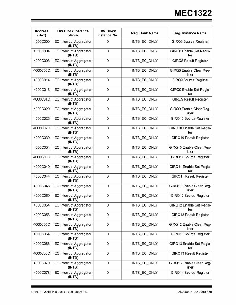
MEC1322
4000C000 EC Interrupt Aggregator (INTS)
0 INTS_EC_ONLY GIRQ8 Source Register
4000C004 EC Interrupt Aggregator (INTS)
0 INTS_EC_ONLY GIRQ8 Enable Set Regis-ter
4000C008 EC Interrupt Aggregator (INTS)
0 INTS_EC_ONLY GIRQ8 Result Register
4000C00C EC Interrupt Aggregator (INTS)
0 INTS_EC_ONLY GIRQ8 Enable Clear Reg-ister
4000C014 EC Interrupt Aggregator (INTS)
0 INTS_EC_ONLY GIRQ9 Source Register
4000C018 EC Interrupt Aggregator (INTS)
0 INTS_EC_ONLY GIRQ9 Enable Set Regis-ter
4000C01C EC Interrupt Aggregator (INTS)
0 INTS_EC_ONLY GIRQ9 Result Register
4000C020 EC Interrupt Aggregator (INTS)
0 INTS_EC_ONLY GIRQ9 Enable Clear Reg-ister
4000C028 EC Interrupt Aggregator (INTS)
0 INTS_EC_ONLY GIRQ10 Source Register
4000C02C EC Interrupt Aggregator (INTS)
0 INTS_EC_ONLY GIRQ10 Enable Set Regis-ter
4000C030 EC Interrupt Aggregator (INTS)
0 INTS_EC_ONLY GIRQ10 Result Register
4000C034 EC Interrupt Aggregator (INTS)
0 INTS_EC_ONLY GIRQ10 Enable Clear Reg-ister
4000C03C EC Interrupt Aggregator (INTS)
0 INTS_EC_ONLY GIRQ11 Source Register
4000C040 EC Interrupt Aggregator (INTS)
0 INTS_EC_ONLY GIRQ11 Enable Set Regis-ter
4000C044 EC Interrupt Aggregator (INTS)
0 INTS_EC_ONLY GIRQ11 Result Register
4000C048 EC Interrupt Aggregator (INTS)
0 INTS_EC_ONLY GIRQ11 Enable Clear Reg-ister
4000C050 EC Interrupt Aggregator (INTS)
0 INTS_EC_ONLY GIRQ12 Source Register
4000C054 EC Interrupt Aggregator (INTS)
0 INTS_EC_ONLY GIRQ12 Enable Set Regis-ter
4000C058 EC Interrupt Aggregator (INTS)
0 INTS_EC_ONLY GIRQ12 Result Register
4000C05C EC Interrupt Aggregator (INTS)
0 INTS_EC_ONLY GIRQ12 Enable Clear Reg-ister
4000C064 EC Interrupt Aggregator (INTS)
0 INTS_EC_ONLY GIRQ13 Source Register
4000C068 EC Interrupt Aggregator (INTS)
0 INTS_EC_ONLY GIRQ13 Enable Set Regis-ter
4000C06C EC Interrupt Aggregator (INTS)
0 INTS_EC_ONLY GIRQ13 Result Register
4000C070 EC Interrupt Aggregator (INTS)
0 INTS_EC_ONLY GIRQ13 Enable Clear Reg-ister
4000C078 EC Interrupt Aggregator (INTS)
0 INTS_EC_ONLY GIRQ14 Source Register
Address (Hex)
HW Block Instance Name
HW Block Instance No.
Reg. Bank Name Reg. Instance Name
2014 - 2015 Microchip Technology Inc. DS00001719D-page 435

MEC1322
4000C07C EC Interrupt Aggregator (INTS)
0 INTS_EC_ONLY GIRQ14 Enable Set Regis-ter
4000C080 EC Interrupt Aggregator (INTS)
0 INTS_EC_ONLY GIRQ14 Result Register
4000C084 EC Interrupt Aggregator (INTS)
0 INTS_EC_ONLY GIRQ14 Enable Clear Reg-ister
4000C08C EC Interrupt Aggregator (INTS)
0 INTS_EC_ONLY GIRQ15 Source Register
4000C090 EC Interrupt Aggregator (INTS)
0 INTS_EC_ONLY GIRQ15 Enable Set Regis-ter
4000C094 EC Interrupt Aggregator (INTS)
0 INTS_EC_ONLY GIRQ15 Result Register
4000C098 EC Interrupt Aggregator (INTS)
0 INTS_EC_ONLY GIRQ15 Enable Clear Reg-ister
4000C0A0 EC Interrupt Aggregator (INTS)
0 INTS_EC_ONLY GIRQ16 Source Register
4000C0A4 EC Interrupt Aggregator (INTS)
0 INTS_EC_ONLY GIRQ16 Enable Set Regis-ter
4000C0A8 EC Interrupt Aggregator (INTS)
0 INTS_EC_ONLY GIRQ16 Result Register
4000C0AC EC Interrupt Aggregator (INTS)
0 INTS_EC_ONLY GIRQ16 Enable Clear Reg-ister
4000C0B4 EC Interrupt Aggregator (INTS)
0 INTS_EC_ONLY GIRQ17 Source Register
4000C0B8 EC Interrupt Aggregator (INTS)
0 INTS_EC_ONLY GIRQ17 Enable Set Regis-ter
4000C0BC EC Interrupt Aggregator (INTS)
0 INTS_EC_ONLY GIRQ17 Result Register
4000C0C0 EC Interrupt Aggregator (INTS)
0 INTS_EC_ONLY GIRQ17 Enable Clear Reg-ister
4000C0C8 EC Interrupt Aggregator (INTS)
0 INTS_EC_ONLY GIRQ18 Source Register
4000C0CC EC Interrupt Aggregator (INTS)
0 INTS_EC_ONLY GIRQ18 Enable Set Regis-ter
4000C0D0 EC Interrupt Aggregator (INTS)
0 INTS_EC_ONLY GIRQ18 Result Register
4000C0D4 EC Interrupt Aggregator (INTS)
0 INTS_EC_ONLY GIRQ18 Enable Clear Reg-ister
4000C0DC EC Interrupt Aggregator (INTS)
0 INTS_EC_ONLY GIRQ19 Source Register
4000C0E0 EC Interrupt Aggregator (INTS)
0 INTS_EC_ONLY GIRQ19 Enable Set Regis-ter
4000C0E4 EC Interrupt Aggregator (INTS)
0 INTS_EC_ONLY GIRQ19 Result Register
4000C0E8 EC Interrupt Aggregator (INTS)
0 INTS_EC_ONLY GIRQ19 Enable Clear Reg-ister
4000C0F0 EC Interrupt Aggregator (INTS)
0 INTS_EC_ONLY GIRQ20 Source Register
4000C0F4 EC Interrupt Aggregator (INTS)
0 INTS_EC_ONLY GIRQ20 Enable Set Regis-ter
Address (Hex)
HW Block Instance Name
HW Block Instance No.
Reg. Bank Name Reg. Instance Name
DS00001719D-page 436 2014 - 2015 Microchip Technology Inc.
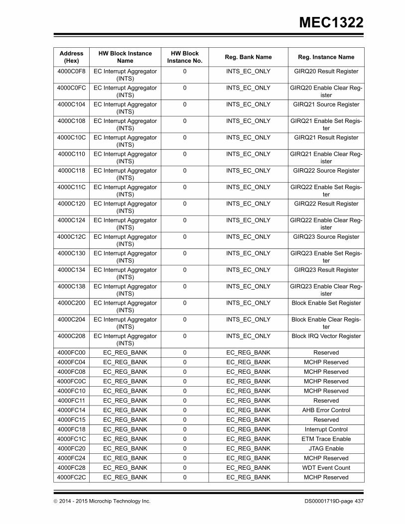
MEC1322
4000C0F8 EC Interrupt Aggregator (INTS)
0 INTS_EC_ONLY GIRQ20 Result Register
4000C0FC EC Interrupt Aggregator (INTS)
0 INTS_EC_ONLY GIRQ20 Enable Clear Reg-ister
4000C104 EC Interrupt Aggregator (INTS)
0 INTS_EC_ONLY GIRQ21 Source Register
4000C108 EC Interrupt Aggregator (INTS)
0 INTS_EC_ONLY GIRQ21 Enable Set Regis-ter
4000C10C EC Interrupt Aggregator (INTS)
0 INTS_EC_ONLY GIRQ21 Result Register
4000C110 EC Interrupt Aggregator (INTS)
0 INTS_EC_ONLY GIRQ21 Enable Clear Reg-ister
4000C118 EC Interrupt Aggregator (INTS)
0 INTS_EC_ONLY GIRQ22 Source Register
4000C11C EC Interrupt Aggregator (INTS)
0 INTS_EC_ONLY GIRQ22 Enable Set Regis-ter
4000C120 EC Interrupt Aggregator (INTS)
0 INTS_EC_ONLY GIRQ22 Result Register
4000C124 EC Interrupt Aggregator (INTS)
0 INTS_EC_ONLY GIRQ22 Enable Clear Reg-ister
4000C12C EC Interrupt Aggregator (INTS)
0 INTS_EC_ONLY GIRQ23 Source Register
4000C130 EC Interrupt Aggregator (INTS)
0 INTS_EC_ONLY GIRQ23 Enable Set Regis-ter
4000C134 EC Interrupt Aggregator (INTS)
0 INTS_EC_ONLY GIRQ23 Result Register
4000C138 EC Interrupt Aggregator (INTS)
0 INTS_EC_ONLY GIRQ23 Enable Clear Reg-ister
4000C200 EC Interrupt Aggregator (INTS)
0 INTS_EC_ONLY Block Enable Set Register
4000C204 EC Interrupt Aggregator (INTS)
0 INTS_EC_ONLY Block Enable Clear Regis-ter
4000C208 EC Interrupt Aggregator (INTS)
0 INTS_EC_ONLY Block IRQ Vector Register
4000FC00 EC_REG_BANK 0 EC_REG_BANK Reserved
4000FC04 EC_REG_BANK 0 EC_REG_BANK MCHP Reserved
4000FC08 EC_REG_BANK 0 EC_REG_BANK MCHP Reserved
4000FC0C EC_REG_BANK 0 EC_REG_BANK MCHP Reserved
4000FC10 EC_REG_BANK 0 EC_REG_BANK MCHP Reserved
4000FC11 EC_REG_BANK 0 EC_REG_BANK Reserved
4000FC14 EC_REG_BANK 0 EC_REG_BANK AHB Error Control
4000FC15 EC_REG_BANK 0 EC_REG_BANK Reserved
4000FC18 EC_REG_BANK 0 EC_REG_BANK Interrupt Control
4000FC1C EC_REG_BANK 0 EC_REG_BANK ETM Trace Enable
4000FC20 EC_REG_BANK 0 EC_REG_BANK JTAG Enable
4000FC24 EC_REG_BANK 0 EC_REG_BANK MCHP Reserved
4000FC28 EC_REG_BANK 0 EC_REG_BANK WDT Event Count
4000FC2C EC_REG_BANK 0 EC_REG_BANK MCHP Reserved
Address (Hex)
HW Block Instance Name
HW Block Instance No.
Reg. Bank Name Reg. Instance Name
2014 - 2015 Microchip Technology Inc. DS00001719D-page 437

MEC1322
4000FC30 EC_REG_BANK 0 EC_REG_BANK MCHP Reserved
4000FC34 EC_REG_BANK 0 EC_REG_BANK MCHP Reserved
4000FC38 EC_REG_BANK 0 EC_REG_BANK ADC VREF PD
4000FC3C EC_REG_BANK 0 EC_REG_BANK MCHP Reserved
4000FC40 EC_REG_BANK 0 EC_REG_BANK MCHP Reserved
40080000 JTAG 0 JTAG_EC_Only JTAG Message OBF
40080004 JTAG 0 JTAG_EC_Only JTAG Message IBF
40080008 JTAG 0 JTAG_EC_Only JTAG OBF Status
40080009 JTAG 0 JTAG_EC_Only JTAG IBF Status
4008000C JTAG 0 JTAG_EC_Only JTAG DBG Ctrl
40080100 PCR 0 PCR Chip Sleep Enable Regis-ter
40080104 PCR 0 PCR Chip Clock Required Reg-ister
40080108 PCR 0 PCR EC Sleep Enables Register
4008010C PCR 0 PCR EC Clock Required Status Register
40080110 PCR 0 PCR Host Sleep Enables Regis-ter
40080114 PCR 0 PCR Host Clock Required Status Register
40080118 PCR 0 PCR CHIP_PCR_ADDR_SYS-_SLEEP_CTRL_0
40080120 PCR 0 PCR Processor Clock Control
40080124 PCR 0 PCR EC Sleep Enable 2 Regis-ter
40080128 PCR 0 PCR EC Clock Required 2 Sta-tus Register
4008012C PCR 0 PCR Slow Clock Control
40080130 PCR 0 PCR Oscillator ID Register
40080134 PCR 0 PCR Reserved
40080138 PCR 0 PCR Chip Reset Enable
4008013C PCR 0 PCR Host Reset Enable
40080140 PCR 0 PCR EC Reset Enable
40080144 PCR 0 PCR EC Reset Enable 2
40080148 PCR 0 PCR PCR Clock Reset Control
40081000 GPIO 0 GPIO Registers GPIO000 Pin Control
40081004 GPIO 0 GPIO Registers GPIO001 Pin Control
40081008 GPIO 0 GPIO Registers GPIO002 Pin Control
4008100C GPIO 0 GPIO Registers GPIO003 Pin Control
40081010 GPIO 0 GPIO Registers GPIO004 Pin Control
40081014 GPIO 0 GPIO Registers GPIO005 Pin Control
40081018 GPIO 0 GPIO Registers GPIO006 Pin Control
4008101C GPIO 0 GPIO Registers GPIO007 Pin Control
40081020 GPIO 0 GPIO Registers GPIO010 Pin Control
Address (Hex)
HW Block Instance Name
HW Block Instance No.
Reg. Bank Name Reg. Instance Name
DS00001719D-page 438 2014 - 2015 Microchip Technology Inc.

MEC1322
40081024 GPIO 0 GPIO Registers GPIO011 Pin Control
40081028 GPIO 0 GPIO Registers GPIO012 Pin Control
4008102C GPIO 0 GPIO Registers GPIO013 Pin Control
40081030 GPIO 0 GPIO Registers GPIO014 Pin Control
40081034 GPIO 0 GPIO Registers GPIO015 Pin Control
40081038 GPIO 0 GPIO Registers GPIO016 Pin Control
4008103C GPIO 0 GPIO Registers GPIO017 Pin Control
40081040 GPIO 0 GPIO Registers GPIO020 Pin Control
40081044 GPIO 0 GPIO Registers GPIO021 Pin Control
40081048 GPIO 0 GPIO Registers GPIO022 Pin Control
4008104C GPIO 0 GPIO Registers GPIO023 Pin Control
40081050 GPIO 0 GPIO Registers GPIO024 Pin Control
40081054 GPIO 0 GPIO Registers GPIO025 Pin Control
40081058 GPIO 0 GPIO Registers GPIO026 Pin Control
4008105C GPIO 0 GPIO Registers GPIO027 Pin Control
40081060 GPIO 0 GPIO Registers GPIO030 Pin Control
40081064 GPIO 0 GPIO Registers GPIO031 Pin Control
40081068 GPIO 0 GPIO Registers GPIO032 Pin Control
4008106C GPIO 0 GPIO Registers GPIO033 Pin Control
40081070 GPIO 0 GPIO Registers GPIO034 Pin Control
40081074 GPIO 0 GPIO Registers GPIO035 Pin Control
40081078 GPIO 0 GPIO Registers GPIO036 Pin Control
40081080 GPIO 0 GPIO Registers GPIO040 Pin Control
40081084 GPIO 0 GPIO Registers GPIO041 Pin Control
40081088 GPIO 0 GPIO Registers GPIO042 Pin Control
4008108C GPIO 0 GPIO Registers GPIO043 Pin Control
40081090 GPIO 0 GPIO Registers GPIO044 Pin Control
40081094 GPIO 0 GPIO Registers GPIO045 Pin Control
40081098 GPIO 0 GPIO Registers GPIO046 Pin Control
4008109C GPIO 0 GPIO Registers GPIO047 Pin Control
400810A0 GPIO 0 GPIO Registers GPIO050 Pin Control
400810A4 GPIO 0 GPIO Registers GPIO051 Pin Control
400810A8 GPIO 0 GPIO Registers GPIO052 Pin Control
400810AC GPIO 0 GPIO Registers GPIO053 Pin Control
400810B0 GPIO 0 GPIO Registers GPIO054 Pin Control
400810B4 GPIO 0 GPIO Registers GPIO055 Pin Control
400810B8 GPIO 0 GPIO Registers GPIO056 Pin Control
400810BC GPIO 0 GPIO Registers GPIO057 Pin Control
400810C0 GPIO 0 GPIO Registers GPIO060 Pin Control
400810C4 GPIO 0 GPIO Registers GPIO061 Pin Control
400810C8 GPIO 0 GPIO Registers GPIO062 Pin Control
400810CC GPIO 0 GPIO Registers GPIO063 Pin Control
400810D0 GPIO 0 GPIO Registers GPIO064 Pin Control
Address (Hex)
HW Block Instance Name
HW Block Instance No.
Reg. Bank Name Reg. Instance Name
2014 - 2015 Microchip Technology Inc. DS00001719D-page 439

MEC1322
400810D4 GPIO 0 GPIO Registers GPIO065 Pin Control
400810D8 GPIO 0 GPIO Registers GPIO066 Pin Control
400810DC GPIO 0 GPIO Registers GPIO067 Pin Control
40081100 GPIO 0 GPIO Registers GPIO100 Pin Control
40081104 GPIO 0 GPIO Registers GPIO101 Pin Control
40081108 GPIO 0 GPIO Registers GPIO102 Pin Control
4008110C GPIO 0 GPIO Registers GPIO103 Pin Control
40081110 GPIO 0 GPIO Registers GPIO104 Pin Control
40081114 GPIO 0 GPIO Registers GPIO105 Pin Control
40081118 GPIO 0 GPIO Registers GPIO106 Pin Control
4008111C GPIO 0 GPIO Registers GPIO107 Pin Control
40081120 GPIO 0 GPIO Registers GPIO110 Pin Control
40081124 GPIO 0 GPIO Registers GPIO111 Pin Control
40081128 GPIO 0 GPIO Registers GPIO112 Pin Control
4008112C GPIO 0 GPIO Registers GPIO113 Pin Control
40081130 GPIO 0 GPIO Registers GPIO114 Pin Control
40081134 GPIO 0 GPIO Registers GPIO115 Pin Control
40081138 GPIO 0 GPIO Registers GPIO116 Pin Control
4008113C GPIO 0 GPIO Registers GPIO117 Pin Control
40081140 GPIO 0 GPIO Registers GPIO120 Pin Control
40081144 GPIO 0 GPIO Registers GPIO121 Pin Control
40081148 GPIO 0 GPIO Registers GPIO122 Pin Control
4008114C GPIO 0 GPIO Registers GPIO123 Pin Control
40081150 GPIO 0 GPIO Registers GPIO124 Pin Control
40081154 GPIO 0 GPIO Registers GPIO125 Pin Control
40081158 GPIO 0 GPIO Registers GPIO126 Pin Control
4008115C GPIO 0 GPIO Registers GPIO127 Pin Control
40081160 GPIO 0 GPIO Registers GPIO130 Pin Control
40081164 GPIO 0 GPIO Registers GPIO131 Pin Control
40081168 GPIO 0 GPIO Registers GPIO132 Pin Control
4008116C GPIO 0 GPIO Registers GPIO133 Pin Control
40081170 GPIO 0 GPIO Registers GPIO134 Pin Control
40081174 GPIO 0 GPIO Registers GPIO135 Pin Control
40081178 GPIO 0 GPIO Registers GPIO136 Pin Control
40081180 GPIO 0 GPIO Registers GPIO140 Pin Control
40081184 GPIO 0 GPIO Registers GPIO141 Pin Control
40081188 GPIO 0 GPIO Registers GPIO142 Pin Control
4008118C GPIO 0 GPIO Registers GPIO143 Pin Control
40081190 GPIO 0 GPIO Registers GPIO144 Pin Control
40081194 GPIO 0 GPIO Registers GPIO145 Pin Control
40081198 GPIO 0 GPIO Registers GPIO146 Pin Control
4008119C GPIO 0 GPIO Registers GPIO147 Pin Control
400811A0 GPIO 0 GPIO Registers GPIO150 Pin Control
Address (Hex)
HW Block Instance Name
HW Block Instance No.
Reg. Bank Name Reg. Instance Name
DS00001719D-page 440 2014 - 2015 Microchip Technology Inc.

MEC1322
400811A4 GPIO 0 GPIO Registers GPIO151 Pin Control
400811A8 GPIO 0 GPIO Registers GPIO152 Pin Control
400811AC GPIO 0 GPIO Registers GPIO153 Pin Control
400811B0 GPIO 0 GPIO Registers GPIO154 Pin Control
400811B4 GPIO 0 GPIO Registers GPIO155 Pin Control
400811B8 GPIO 0 GPIO Registers GPIO156 Pin Control
400811BC GPIO 0 GPIO Registers GPIO157 Pin Control
400811C0 GPIO 0 GPIO Registers GPIO160 Pin Control
400811C4 GPIO 0 GPIO Registers GPIO161 Pin Control
400811C8 GPIO 0 GPIO Registers GPIO162 Pin Control
400811CC GPIO 0 GPIO Registers GPIO163 Pin Control
400811D0 GPIO 0 GPIO Registers GPIO164 Pin Control
400811D4 GPIO 0 GPIO Registers GPIO165 Pin Control
40081200 GPIO 0 GPIO Registers GPIO200 Pin Control
40081204 GPIO 0 GPIO Registers GPIO201 Pin Control
40081208 GPIO 0 GPIO Registers GPIO202 Pin Control
4008120C GPIO 0 GPIO Registers GPIO203 Pin Control
40081210 GPIO 0 GPIO Registers GPIO204 Pin Control
40081214 GPIO 0 GPIO Registers Reserved
40081218 GPIO 0 GPIO Registers GPIO206 Pin Control
4008121C GPIO 0 GPIO Registers Reserved
40081220 GPIO 0 GPIO Registers GPIO210 Pin Control
40081224 GPIO 0 GPIO Registers GPIO211 Pin Control
40081280 GPIO 0 GPIO Registers Output GPIO[000:036]
40081284 GPIO 0 GPIO Registers Output GPIO[040:076]
40081288 GPIO 0 GPIO Registers Output GPIO[100:136]
4008128C GPIO 0 GPIO Registers Output GPIO[140:176]
40081290 GPIO 0 GPIO Registers Output GPIO[200:236]
40081300 GPIO 0 GPIO Registers Input GPIO[000:036]
40081304 GPIO 0 GPIO Registers Input GPIO[040:076]
40081308 GPIO 0 GPIO Registers Input GPIO[100:136]
4008130C GPIO 0 GPIO Registers Input GPIO[140:176]
40081310 GPIO 0 GPIO Registers Input GPIO[200:236]
40081314 GPIO 0 GPIO Registers Reserved
40081500 GPIO 0 GPIO Registers GPIO000 Pin Control 2
40081504 GPIO 0 GPIO Registers GPIO001 Pin Control 2
40081508 GPIO 0 GPIO Registers GPIO002 Pin Control 2
4008150C GPIO 0 GPIO Registers GPIO003 Pin Control 2
40081510 GPIO 0 GPIO Registers GPIO004 Pin Control 2
40081514 GPIO 0 GPIO Registers GPIO005 Pin Control 2
40081518 GPIO 0 GPIO Registers GPIO006 Pin Control 2
4008151C GPIO 0 GPIO Registers GPIO007 Pin Control 2
40081520 GPIO 0 GPIO Registers GPIO010 Pin Control 2
Address (Hex)
HW Block Instance Name
HW Block Instance No.
Reg. Bank Name Reg. Instance Name
2014 - 2015 Microchip Technology Inc. DS00001719D-page 441

MEC1322
40081524 GPIO 0 GPIO Registers GPIO011 Pin Control 2
40081528 GPIO 0 GPIO Registers GPIO012 Pin Control 2
4008152C GPIO 0 GPIO Registers GPIO013 Pin Control 2
40081530 GPIO 0 GPIO Registers GPIO014 Pin Control 2
40081534 GPIO 0 GPIO Registers GPIO015 Pin Control 2
40081538 GPIO 0 GPIO Registers GPIO016 Pin Control 2
4008153C GPIO 0 GPIO Registers GPIO017 Pin Control 2
40081540 GPIO 0 GPIO Registers GPIO020 Pin Control 2
40081544 GPIO 0 GPIO Registers GPIO021 Pin Control 2
40081548 GPIO 0 GPIO Registers GPIO022 Pin Control 2
4008154C GPIO 0 GPIO Registers GPIO023 Pin Control 2
40081550 GPIO 0 GPIO Registers GPIO024 Pin Control 2
40081554 GPIO 0 GPIO Registers GPIO025 Pin Control 2
40081558 GPIO 0 GPIO Registers GPIO026 Pin Control 2
4008155C GPIO 0 GPIO Registers GPIO027 Pin Control 2
40081560 GPIO 0 GPIO Registers GPIO030 Pin Control 2
40081564 GPIO 0 GPIO Registers GPIO031 Pin Control 2
40081568 GPIO 0 GPIO Registers GPIO032 Pin Control 2
4008156C GPIO 0 GPIO Registers GPIO033 Pin Control 2
40081570 GPIO 0 GPIO Registers GPIO034 Pin Control 2
40081574 GPIO 0 GPIO Registers GPIO035 Pin Control 2
40081578 GPIO 0 GPIO Registers GPIO036 Pin Control 2
40081580 GPIO 0 GPIO Registers GPIO040 Pin Control 2
40081584 GPIO 0 GPIO Registers GPIO041 Pin Control 2
40081588 GPIO 0 GPIO Registers GPIO042 Pin Control 2
4008158C GPIO 0 GPIO Registers GPIO043 Pin Control 2
40081590 GPIO 0 GPIO Registers GPIO044 Pin Control 2
40081594 GPIO 0 GPIO Registers GPIO045 Pin Control 2
40081598 GPIO 0 GPIO Registers GPIO046 Pin Control 2
4008159C GPIO 0 GPIO Registers GPIO047 Pin Control 2
400815A0 GPIO 0 GPIO Registers GPIO050 Pin Control 2
400815A4 GPIO 0 GPIO Registers GPIO051 Pin Control 2
400815A8 GPIO 0 GPIO Registers GPIO052 Pin Control 2
400815AC GPIO 0 GPIO Registers GPIO053 Pin Control 2
400815B0 GPIO 0 GPIO Registers GPIO054 Pin Control 2
400815B4 GPIO 0 GPIO Registers GPIO055 Pin Control 2
400815B8 GPIO 0 GPIO Registers GPIO056 Pin Control 2
400815BC GPIO 0 GPIO Registers GPIO057 Pin Control 2
400815C0 GPIO 0 GPIO Registers GPIO060 Pin Control 2
400815C4 GPIO 0 GPIO Registers GPIO061 Pin Control 2
400815C8 GPIO 0 GPIO Registers GPIO062 Pin Control 2
400815CC GPIO 0 GPIO Registers GPIO063 Pin Control 2
400815D0 GPIO 0 GPIO Registers GPIO064 Pin Control 2
Address (Hex)
HW Block Instance Name
HW Block Instance No.
Reg. Bank Name Reg. Instance Name
DS00001719D-page 442 2014 - 2015 Microchip Technology Inc.

MEC1322
400815D4 GPIO 0 GPIO Registers GPIO065 Pin Control 2
400815D8 GPIO 0 GPIO Registers GPIO066 Pin Control 2
400815DC GPIO 0 GPIO Registers GPIO067 Pin Control 2
400815E0 GPIO 0 GPIO Registers GPIO100 Pin Control 2
400815E4 GPIO 0 GPIO Registers GPIO101 Pin Control 2
400815E8 GPIO 0 GPIO Registers GPIO102 Pin Control 2
400815EC GPIO 0 GPIO Registers GPIO103 Pin Control 2
400815F0 GPIO 0 GPIO Registers GPIO104 Pin Control 2
400815F4 GPIO 0 GPIO Registers GPIO105 Pin Control 2
400815F8 GPIO 0 GPIO Registers GPIO106 Pin Control 2
400815FC GPIO 0 GPIO Registers GPIO107 Pin Control 2
40081600 GPIO 0 GPIO Registers GPIO110 Pin Control 2
40081604 GPIO 0 GPIO Registers GPIO111 Pin Control 2
40081608 GPIO 0 GPIO Registers GPIO112 Pin Control 2
4008160C GPIO 0 GPIO Registers GPIO113 Pin Control 2
40081610 GPIO 0 GPIO Registers GPIO114 Pin Control 2
40081614 GPIO 0 GPIO Registers GPIO115 Pin Control 2
40081618 GPIO 0 GPIO Registers GPIO116 Pin Control 2
4008161C GPIO 0 GPIO Registers GPIO117 Pin Control 2
40081620 GPIO 0 GPIO Registers GPIO120 Pin Control 2
40081624 GPIO 0 GPIO Registers GPIO121 Pin Control 2
40081628 GPIO 0 GPIO Registers GPIO122 Pin Control 2
4008162C GPIO 0 GPIO Registers GPIO123 Pin Control 2
40081630 GPIO 0 GPIO Registers GPIO124 Pin Control 2
40081634 GPIO 0 GPIO Registers GPIO125 Pin Control 2
40081638 GPIO 0 GPIO Registers GPIO126 Pin Control 2
4008163C GPIO 0 GPIO Registers GPIO127 Pin Control 2
40081640 GPIO 0 GPIO Registers GPIO130 Pin Control 2
40081644 GPIO 0 GPIO Registers GPIO131 Pin Control 2
40081648 GPIO 0 GPIO Registers GPIO132 Pin Control 2
4008164C GPIO 0 GPIO Registers GPIO133 Pin Control 2
40081650 GPIO 0 GPIO Registers GPIO134 Pin Control 2
40081654 GPIO 0 GPIO Registers GPIO135 Pin Control 2
40081658 GPIO 0 GPIO Registers GPIO136 Pin Control 2
40081660 GPIO 0 GPIO Registers GPIO140 Pin Control 2
40081664 GPIO 0 GPIO Registers GPIO141 Pin Control 2
40081668 GPIO 0 GPIO Registers GPIO142 Pin Control 2
4008166C GPIO 0 GPIO Registers GPIO143 Pin Control 2
40081670 GPIO 0 GPIO Registers GPIO144 Pin Control 2
40081674 GPIO 0 GPIO Registers GPIO145 Pin Control 2
40081678 GPIO 0 GPIO Registers GPIO146 Pin Control 2
4008167C GPIO 0 GPIO Registers GPIO147 Pin Control 2
40081680 GPIO 0 GPIO Registers GPIO150 Pin Control 2
Address (Hex)
HW Block Instance Name
HW Block Instance No.
Reg. Bank Name Reg. Instance Name
2014 - 2015 Microchip Technology Inc. DS00001719D-page 443

MEC1322
40081684 GPIO 0 GPIO Registers GPIO151 Pin Control 2
40081688 GPIO 0 GPIO Registers GPIO152 Pin Control 2
4008168C GPIO 0 GPIO Registers GPIO153 Pin Control 2
40081690 GPIO 0 GPIO Registers GPIO154 Pin Control 2
40081694 GPIO 0 GPIO Registers GPIO155 Pin Control 2
40081698 GPIO 0 GPIO Registers GPIO156 Pin Control 2
4008169C GPIO 0 GPIO Registers GPIO157 Pin Control 2
400816A0 GPIO 0 GPIO Registers GPIO160 Pin Control 2
400816A4 GPIO 0 GPIO Registers GPIO161 Pin Control 2
400816A8 GPIO 0 GPIO Registers GPIO162 Pin Control 2
400816AC GPIO 0 GPIO Registers GPIO163 Pin Control 2
400816B0 GPIO 0 GPIO Registers GPIO164 Pin Control 2
400816B4 GPIO 0 GPIO Registers GPIO165 Pin Control 2
40081720 GPIO 0 GPIO Registers GPIO200 Pin Control 2
40081724 GPIO 0 GPIO Registers GPIO201 Pin Control 2
40081728 GPIO 0 GPIO Registers GPIO202 Pin Control 2
4008172C GPIO 0 GPIO Registers GPIO203 Pin Control 2
40081730 GPIO 0 GPIO Registers GPIO204 Pin Control 2
40081738 GPIO 0 GPIO Registers GPIO206 Pin Control 2
40081740 GPIO 0 GPIO Registers GPIO210 Pin Control 2
40081744 GPIO 0 GPIO Registers GPIO211 Pin Control 2
400F0000 IMAP 0 EMI_RUNTIME EMI Host-to-EC Mailbox Register
400F0001 IMAP 0 EMI_RUNTIME EC-to-Host Mailbox Regis-ter
400F0002 IMAP 0 EMI_RUNTIME EC Address Register
400F0004 IMAP 0 EMI_RUNTIME EC Data Register
400F0008 IMAP 0 EMI_RUNTIME Interrupt Source Register
400F000A IMAP 0 EMI_RUNTIME Interrupt Mask Register
400F000C IMAP 0 EMI_RUNTIME Application ID Register
400F0100 IMAP 0 EMI_EC_ONLY EMI Host-to-EC Mailbox Register
400F0101 IMAP 0 EMI_EC_ONLY EC-to-Host Mailbox Regis-ter
400F0104 IMAP 0 EMI_EC_ONLY Memory Base Address 0 Register
400F0108 IMAP 0 EMI_EC_ONLY Memory Read Limit 0 Reg-ister
400F010A IMAP 0 EMI_EC_ONLY Memory Write Limit 0 Reg-ister
400F010C IMAP 0 EMI_EC_ONLY Memory Base Address 1 Register
400F0110 IMAP 0 EMI_EC_ONLY Memory Read Limit 1 Reg-ister
400F0112 IMAP 0 EMI_EC_ONLY Memory Write Limit 1 Reg-ister
Address (Hex)
HW Block Instance Name
HW Block Instance No.
Reg. Bank Name Reg. Instance Name
DS00001719D-page 444 2014 - 2015 Microchip Technology Inc.

MEC1322
400F0114 IMAP 0 EMI_EC_ONLY Interrupt Set Register
400F0116 IMAP 0 EMI_EC_ONLY Host Clear Enable Register
400F0400 8042 Host Interface 0 KBC_Runtime EC_Host Data/Aux Regis-ter (Read)
400F0400 8042 Host Interface 0 KBC_Runtime Host_EC Data Register (Write)
400F0404 8042 Host Interface 0 KBC_Runtime Host_EC Command Regis-ter (Write)
400F0404 8042 Host Interface 0 KBC_Runtime Keyboard Status Read Register
400F0500 8042 Host Interface 0 KBC_EC_Only Host_EC Data/Cmd Regis-ter
400F0500 8042 Host Interface 0 KBC_EC_Only EC_Host Data Register
400F0504 8042 Host Interface 0 KBC_EC_Only Keyboard Status Read Register
400F0508 8042 Host Interface 0 KBC_EC_Only Keyboard Control Register
400F050C 8042 Host Interface 0 KBC_EC_Only EC_Host Aux Register
400F0514 8042 Host Interface 0 KBC_EC_Only PCOBF Register
400F0730 8042 Host Interface 0 KBC_Configuration Activate Register
400F0C00 ACPI EC Interface 0 ACPI_Runtime ACPI OS Data Register Byte 0
400F0C00 ACPI EC Interface 0 ACPI_Runtime ACPI OS Data Register Byte 0
400F0C01 ACPI EC Interface 0 ACPI_Runtime ACPI OS Data Register Byte 1
400F0C01 ACPI EC Interface 0 ACPI_Runtime ACPI OS Data Register Byte 1
400F0C02 ACPI EC Interface 0 ACPI_Runtime ACPI OS Data Register Byte 2
400F0C02 ACPI EC Interface 0 ACPI_Runtime ACPI OS Data Register Byte 2
400F0C03 ACPI EC Interface 0 ACPI_Runtime ACPI OS Data Register Byte 3
400F0C03 ACPI EC Interface 0 ACPI_Runtime ACPI OS Data Register Byte 3
400F0C04 ACPI EC Interface 0 ACPI_Runtime ACPI OS Command Regis-ter
400F0C04 ACPI EC Interface 0 ACPI_Runtime STATUS OS-Register
400F0C05 ACPI EC Interface 0 ACPI_Runtime Byte Control OS-Register
400F0D00 ACPI EC Interface 0 ACPI_EC_Only EC2OS Data EC-Register Byte 0
400F0D01 ACPI EC Interface 0 ACPI_EC_Only EC2OS Data EC-Register Byte 1
400F0D02 ACPI EC Interface 0 ACPI_EC_Only EC2OS Data EC-Register Byte 2
400F0D03 ACPI EC Interface 0 ACPI_EC_Only EC2OS Data EC-Register Byte 3
400F0D04 ACPI EC Interface 0 ACPI_EC_Only STATUS EC-Register
Address (Hex)
HW Block Instance Name
HW Block Instance No.
Reg. Bank Name Reg. Instance Name
2014 - 2015 Microchip Technology Inc. DS00001719D-page 445

MEC1322
400F0D05 ACPI EC Interface 0 ACPI_EC_Only Byte Control EC-Register
400F0D08 ACPI EC Interface 0 ACPI_EC_Only OS2EC Data EC-Register Byte 0
400F0D08 ACPI EC Interface 0 ACPI_EC_Only OS2EC Data EC-Register Byte 0
400F0D09 ACPI EC Interface 0 ACPI_EC_Only OS2EC Data EC-Register Byte 1
400F0D0A ACPI EC Interface 0 ACPI_EC_Only OS2EC Data EC-Register Byte 2
400F0D0B ACPI EC Interface 0 ACPI_EC_Only OS2EC Data EC-Register Byte 3
400F1000 ACPI EC Interface 1 ACPI_Runtime ACPI OS Data Register Byte 0
400F1000 ACPI EC Interface 1 ACPI_Runtime ACPI OS Data Register Byte 0
400F1001 ACPI EC Interface 1 ACPI_Runtime ACPI OS Data Register Byte 1
400F1001 ACPI EC Interface 1 ACPI_Runtime ACPI OS Data Register Byte 1
400F1002 ACPI EC Interface 1 ACPI_Runtime ACPI OS Data Register Byte 2
400F1002 ACPI EC Interface 1 ACPI_Runtime ACPI OS Data Register Byte 2
400F1003 ACPI EC Interface 1 ACPI_Runtime ACPI OS Data Register Byte 3
400F1003 ACPI EC Interface 1 ACPI_Runtime ACPI OS Data Register Byte 3
400F1004 ACPI EC Interface 1 ACPI_Runtime ACPI OS Command Regis-ter
400F1004 ACPI EC Interface 1 ACPI_Runtime STATUS OS-Register
400F1005 ACPI EC Interface 1 ACPI_Runtime Byte Control OS-Register
400F1100 ACPI EC Interface 1 ACPI_EC_Only EC2OS Data EC-Register Byte 0
400F1101 ACPI EC Interface 1 ACPI_EC_Only EC2OS Data EC-Register Byte 1
400F1102 ACPI EC Interface 1 ACPI_EC_Only EC2OS Data EC-Register Byte 2
400F1103 ACPI EC Interface 1 ACPI_EC_Only EC2OS Data EC-Register Byte 3
400F1104 ACPI EC Interface 1 ACPI_EC_Only STATUS EC-Register
400F1105 ACPI EC Interface 1 ACPI_EC_Only Byte Control EC-Register
400F1108 ACPI EC Interface 1 ACPI_EC_Only OS2EC Data EC-Register Byte 0
400F1108 ACPI EC Interface 1 ACPI_EC_Only OS2EC Data EC-Register Byte 0
400F1109 ACPI EC Interface 1 ACPI_EC_Only OS2EC Data EC-Register Byte 1
400F110A ACPI EC Interface 1 ACPI_EC_Only OS2EC Data EC-Register Byte 2
Address (Hex)
HW Block Instance Name
HW Block Instance No.
Reg. Bank Name Reg. Instance Name
DS00001719D-page 446 2014 - 2015 Microchip Technology Inc.

MEC1322
400F110B ACPI EC Interface 1 ACPI_EC_Only OS2EC Data EC-Register Byte 3
400F1400 ACPI PM1 0 PM1_Runtime PM1 Status 1
400F1401 ACPI PM1 0 PM1_Runtime PM1 Status 2
400F1402 ACPI PM1 0 PM1_Runtime PM1 Enable 1
400F1403 ACPI PM1 0 PM1_Runtime PM1 Enable 2
400F1404 ACPI PM1 0 PM1_Runtime PM1 Control 1
400F1405 ACPI PM1 0 PM1_Runtime PM1 Control 2
400F1406 ACPI PM1 0 PM1_Runtime PM2 Control 1
400F1407 ACPI PM1 0 PM1_Runtime PM2 Control 2
400F1500 ACPI PM1 0 PM1_EC_Only PM1 Status 1
400F1501 ACPI PM1 0 PM1_EC_Only PM1 Status 2
400F1502 ACPI PM1 0 PM1_EC_Only PM1 Enable 1
400F1503 ACPI PM1 0 PM1_EC_Only PM1 Enable 2
400F1504 ACPI PM1 0 PM1_EC_Only PM1 Control 1
400F1505 ACPI PM1 0 PM1_EC_Only PM1 Control 2
400F1506 ACPI PM1 0 PM1_EC_Only PM2 Control 1
400F1507 ACPI PM1 0 PM1_EC_Only PM2 Control 2
400F1510 ACPI PM1 0 PM1_EC_Only PM1 EC PM Status
400F1800 8042 Host Interface 0 Legacy_Runtime PORT92 Register
400F1900 8042 Host Interface 0 Legacy_EC_Only GATEA20 Control Register
400F1908 8042 Host Interface 0 Legacy_EC_Only SETGA20L Register
400F190C 8042 Host Interface 0 Legacy_EC_Only RSTGA20L Register
400F1B30 8042 Host Interface 0 Legacy_Configuration PORT92 Enable Register
400F1C00 M16C550A UART 0 UART_EC_Only UART Programmable BAUD Rate Generator
(LSB) Register
400F1C00 M16C550A UART 0 UART_EC_Only UART Receive Buffer Reg-ister
400F1C00 M16C550A UART 0 UART_EC_Only UART Transmit Buffer Reg-ister
400F1C01 M16C550A UART 0 UART_EC_Only UART Programmable BAUD Rate Generator
(MSB) Register
400F1C01 M16C550A UART 0 UART_EC_Only UART Interrupt Enable Register
400F1C02 M16C550A UART 0 UART_EC_Only UART FIFO Control Regis-ter
400F1C02 M16C550A UART 0 UART_EC_Only UART Interrupt Identifica-tion Register
400F1C03 M16C550A UART 0 UART_EC_Only UART Line Control Regis-ter
400F1C04 M16C550A UART 0 UART_EC_Only UART Modem Control Register
400F1C05 M16C550A UART 0 UART_EC_Only UART Line Status Register
Address (Hex)
HW Block Instance Name
HW Block Instance No.
Reg. Bank Name Reg. Instance Name
2014 - 2015 Microchip Technology Inc. DS00001719D-page 447

MEC1322
400F1C06 M16C550A UART 0 UART_EC_Only UART Modem Status Reg-ister
400F1C07 M16C550A UART 0 UART_EC_Only UART Scratchpad Register
400F1C00 M16C550A UART 0 UART_Runtime UART Transmit Buffer Reg-ister
400F1C00 M16C550A UART 0 UART_Runtime UART Programmable BAUD Rate Generator
(LSB) Register
400F1C00 M16C550A UART 0 UART_Runtime UART Receive Buffer Reg-ister
400F1C01 M16C550A UART 0 UART_Runtime UART Interrupt Enable Register
400F1C01 M16C550A UART 0 UART_Runtime UART Programmable BAUD Rate Generator
(MSB) Register
400F1C02 M16C550A UART 0 UART_Runtime UART FIFO Control Regis-ter
400F1C02 M16C550A UART 0 UART_Runtime UART Interrupt Identifica-tion Register
400F1C03 M16C550A UART 0 UART_Runtime UART Line Control Regis-ter
400F1C04 M16C550A UART 0 UART_Runtime UART Modem Control Register
400F1C05 M16C550A UART 0 UART_Runtime UART Line Status Register
400F1C06 M16C550A UART 0 UART_Runtime UART Modem Status Reg-ister
400F1C07 M16C550A UART 0 UART_Runtime UART Scratchpad Register
400F1F30 M16C550A UART 0 UART_Config UART Activate Register
400F1FF0 M16C550A UART 0 UART_Config UART Config Select Regis-ter
400F2400 Mailbox Registers Inter-face
0 MBX_Runtime MBX_Index Register
400F2401 Mailbox Registers Inter-face
0 MBX_Runtime MBX_Data_Register
400F2500 Mailbox Registers Inter-face
0 MBX_EC_Only HOST-to-EC Mailbox Reg-ister
400F2504 Mailbox Registers Inter-face
0 MBX_EC_Only EC-to-Host Mailbox Regis-ter
400F2508 Mailbox Registers Inter-face
0 MBX_EC_Only SMI Interrupt Source Reg-ister
400F250C Mailbox Registers Inter-face
0 MBX_EC_Only SMI Interrupt Mask Regis-ter
400F2510 Mailbox Registers Inter-face
0 MBX_EC_Only Mailbox Register [3:0]
400F2514 Mailbox Registers Inter-face
0 MBX_EC_Only Mailbox Register [7:4]
400F2518 Mailbox Registers Inter-face
0 MBX_EC_Only Mailbox Register [Bh:8]
Address (Hex)
HW Block Instance Name
HW Block Instance No.
Reg. Bank Name Reg. Instance Name
DS00001719D-page 448 2014 - 2015 Microchip Technology Inc.
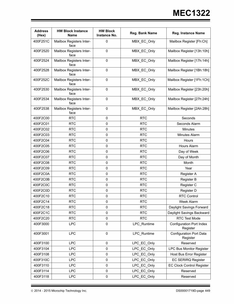
MEC1322
400F251C Mailbox Registers Inter-face
0 MBX_EC_Only Mailbox Register [Fh:Ch]
400F2520 Mailbox Registers Inter-face
0 MBX_EC_Only Mailbox Register [13h:10h]
400F2524 Mailbox Registers Inter-face
0 MBX_EC_Only Mailbox Register [17h:14h]
400F2528 Mailbox Registers Inter-face
0 MBX_EC_Only Mailbox Register [1Bh:18h]
400F252C Mailbox Registers Inter-face
0 MBX_EC_Only Mailbox Register [1Fh:1Ch]
400F2530 Mailbox Registers Inter-face
0 MBX_EC_Only Mailbox Register [23h:20h]
400F2534 Mailbox Registers Inter-face
0 MBX_EC_Only Mailbox Register [27h:24h]
400F2538 Mailbox Registers Inter-face
0 MBX_EC_Only Mailbox Register [2Ah:28h]
400F2C00 RTC 0 RTC Seconds
400F2C01 RTC 0 RTC Seconds Alarm
400F2C02 RTC 0 RTC Minutes
400F2C03 RTC 0 RTC Minutes Alarm
400F2C04 RTC 0 RTC Hours
400F2C05 RTC 0 RTC Hours Alarm
400F2C06 RTC 0 RTC Day of Week
400F2C07 RTC 0 RTC Day of Month
400F2C08 RTC 0 RTC Month
400F2C09 RTC 0 RTC Year
400F2C0A RTC 0 RTC Register A
400F2C0B RTC 0 RTC Register B
400F2C0C RTC 0 RTC Register C
400F2C0D RTC 0 RTC Register D
400F2C10 RTC 0 RTC RTC Control
400F2C14 RTC 0 RTC Week Alarm
400F2C18 RTC 0 RTC Daylight Savings Forward
400F2C1C RTC 0 RTC Daylight Savings Backward
400F2C20 RTC 0 RTC RTC Test Mode
400F3000 LPC 0 LPC_Runtime Configuration Port Index Register
400F3001 LPC 0 LPC_Runtime Configuration Port Data Register
400F3100 LPC 0 LPC_EC_Only Reserved
400F3104 LPC 0 LPC_EC_Only LPC Bus Monitor Register
400F3108 LPC 0 LPC_EC_Only Host Bus Error Register
400F310C LPC 0 LPC_EC_Only EC SERIRQ Register
400F3110 LPC 0 LPC_EC_Only EC Clock Control Register
400F3114 LPC 0 LPC_EC_Only Reserved
400F3118 LPC 0 LPC_EC_Only Reserved
Address (Hex)
HW Block Instance Name
HW Block Instance No.
Reg. Bank Name Reg. Instance Name
2014 - 2015 Microchip Technology Inc. DS00001719D-page 449
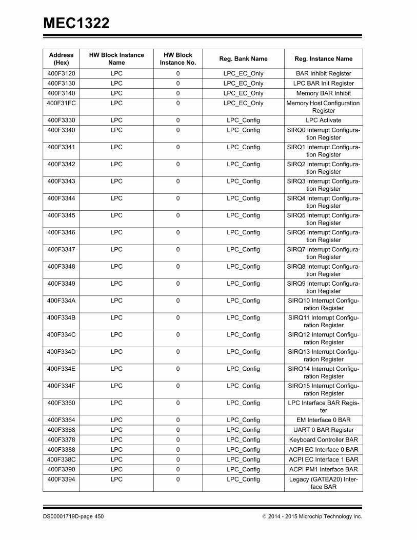
MEC1322
400F3120 LPC 0 LPC_EC_Only BAR Inhibit Register
400F3130 LPC 0 LPC_EC_Only LPC BAR Init Register
400F3140 LPC 0 LPC_EC_Only Memory BAR Inhibit
400F31FC LPC 0 LPC_EC_Only Memory Host Configuration Register
400F3330 LPC 0 LPC_Config LPC Activate
400F3340 LPC 0 LPC_Config SIRQ0 Interrupt Configura-tion Register
400F3341 LPC 0 LPC_Config SIRQ1 Interrupt Configura-tion Register
400F3342 LPC 0 LPC_Config SIRQ2 Interrupt Configura-tion Register
400F3343 LPC 0 LPC_Config SIRQ3 Interrupt Configura-tion Register
400F3344 LPC 0 LPC_Config SIRQ4 Interrupt Configura-tion Register
400F3345 LPC 0 LPC_Config SIRQ5 Interrupt Configura-tion Register
400F3346 LPC 0 LPC_Config SIRQ6 Interrupt Configura-tion Register
400F3347 LPC 0 LPC_Config SIRQ7 Interrupt Configura-tion Register
400F3348 LPC 0 LPC_Config SIRQ8 Interrupt Configura-tion Register
400F3349 LPC 0 LPC_Config SIRQ9 Interrupt Configura-tion Register
400F334A LPC 0 LPC_Config SIRQ10 Interrupt Configu-ration Register
400F334B LPC 0 LPC_Config SIRQ11 Interrupt Configu-ration Register
400F334C LPC 0 LPC_Config SIRQ12 Interrupt Configu-ration Register
400F334D LPC 0 LPC_Config SIRQ13 Interrupt Configu-ration Register
400F334E LPC 0 LPC_Config SIRQ14 Interrupt Configu-ration Register
400F334F LPC 0 LPC_Config SIRQ15 Interrupt Configu-ration Register
400F3360 LPC 0 LPC_Config LPC Interface BAR Regis-ter
400F3364 LPC 0 LPC_Config EM Interface 0 BAR
400F3368 LPC 0 LPC_Config UART 0 BAR Register
400F3378 LPC 0 LPC_Config Keyboard Controller BAR
400F3388 LPC 0 LPC_Config ACPI EC Interface 0 BAR
400F338C LPC 0 LPC_Config ACPI EC Interface 1 BAR
400F3390 LPC 0 LPC_Config ACPI PM1 Interface BAR
400F3394 LPC 0 LPC_Config Legacy (GATEA20) Inter-face BAR
Address (Hex)
HW Block Instance Name
HW Block Instance No.
Reg. Bank Name Reg. Instance Name
DS00001719D-page 450 2014 - 2015 Microchip Technology Inc.

MEC1322
400F3398 LPC 0 LPC_Config Mailbox Registers Interface BAR
400F33C0 LPC 0 LPC_Config Mailbox Registers I/F Mem-ory BAR
400F33C6 LPC 0 LPC_Config ACPI EC Interface 0 Mem-ory BAR
400F33CC LPC 0 LPC_Config ACPI EC Interface 1 Mem-ory BAR
400F33D2 LPC 0 LPC_Config EM Interface 0 Memory BAR
400FFF00 Global Configuration Registers
0 GCR GCR Reserved Registers
400FFF07 Global Configuration Registers
0 GCR Logical Device Number Register
400FFF08 Global Configuration Registers
0 GCR GCR Reserved Registers
400FFF20 Global Configuration Registers
0 GCR Device ID Register
400FFF21 Global Configuration Registers
0 GCR Device Revision Hard Wired Register
400FFF22 Global Configuration Registers
0 GCR GCR Reserved
400FFF25 Global Configuration Registers
0 GCR GCR Reserved
400FFF28 Global Configuration Registers
0 GCR GCR Build Register
400FFF2A Global Configuration Registers
0 GCR GCR Reserved Registers
400FFF2C Global Configuration Registers
0 GCR GCR Scratch Register
Address (Hex)
HW Block Instance Name
HW Block Instance No.
Reg. Bank Name Reg. Instance Name
2014 - 2015 Microchip Technology Inc. DS00001719D-page 451

MEC1322
DS00001719D-page 452 2014 - 2015 Microchip Technology Inc.
APPENDIX A: REVISION HISTORY
TABLE A-1: DATA SHEET REVISION HISTORY
Revision Section/Figure/Entry Correction
DS00001719D (09-14-15 Table 37-1, "Absolute Maximum Ther-mal Ratings", Table 37-8, "Thermal Operating Conditions" and Table 37-10, "VCC1 Supply Current, I_VCC1"
Updated tables to add Industrial tem-perature information.
Table 37-11, "VBAT Supply Current, I_VBAT (VBAT=3.0V)" and Table 37-12, "VBAT Supply Current, I_VBAT (VBAT=3.3V)"
Updated tables to remove internal 32kHz oscillator information.
Product Identification System Added industrial ordering information.
DS00001719C (06-15-15) Table 27-9, "EC-Only Register Base Address Table"
Updated Base addresses
Table 15-3, "Interrupt Event Aggrega-tor Routing Summary" and Table 15-22, "Bit definitions for GIRQ19 Source, Enable, and Result Registers"
Updated locations for LRESET# and VCC_PWRGD bits
Section 29.15.4, "PS2 Status Regis-ter"
Updated description of REC_TIMEOUT bit
Table 37-8, "Thermal Operating Con-ditions" and Table 37-9, "Thermal Packaging Characteristics"
Updated tables.
Product Features Added 144 WFBGA package
Table 1-3, "MEC1322 144 WFBGA Pin Configuration",Figure 1-1, "MEC1322 PIN NAME TO 144-PIN WFBGA BALL MAPPING (TOP)" and Figure 1-5, "144-pin WFBGA Package Outline"
Added 144 WFBGA pinout and package drawing.
Product Identification System Added 144 WFBGA package ordering information
Section 8.0, "RAM and ROM" Described the distinction between SRAM optimized for instructions and optimized for data.
Section 20.7, "Pin Multiplexing Con-trol"
Updated note on GPIO pins that do not exist in the 128 pin package.
DS00001719B (06-03-14) Throughout document
PIS page
Features
Part number changed from MEC1322/24 to MEC1322.
“C0” added to package information
Sub-bullet added following “LPC Inter-face”: “Supports LPC Bus frequencies of 19MHz to 33MHz”.
DS00001719A (04-14-14) REV A - Document Release

2014 - 2015 Microchip Technology Inc. DS00001719D-page 453
MEC1322
THE MICROCHIP WEB SITE
Microchip provides online support via our WWW site at www.microchip.com. This web site is used as a means to makefiles and information easily available to customers. Accessible by using your favorite Internet browser, the web site con-tains the following information:
• Product Support – Data sheets and errata, application notes and sample programs, design resources, user’s guides and hardware support documents, latest software releases and archived software
• General Technical Support – Frequently Asked Questions (FAQ), technical support requests, online discussion groups, Microchip consultant program member listing
• Business of Microchip – Product selector and ordering guides, latest Microchip press releases, listing of semi-nars and events, listings of Microchip sales offices, distributors and factory representatives
CUSTOMER CHANGE NOTIFICATION SERVICE
Microchip’s customer notification service helps keep customers current on Microchip products. Subscribers will receivee-mail notification whenever there are changes, updates, revisions or errata related to a specified product family ordevelopment tool of interest.
To register, access the Microchip web site at www.microchip.com. Under “Support”, click on “Customer Change Notifi-cation” and follow the registration instructions.
CUSTOMER SUPPORT
Users of Microchip products can receive assistance through several channels:
• Distributor or Representative
• Local Sales Office
• Field Application Engineer (FAE)
• Technical Support
Customers should contact their distributor, representative or field application engineer (FAE) for support. Local salesoffices are also available to help customers. A listing of sales offices and locations is included in the back of this docu-ment.
Technical support is available through the web site at: http://microchip.com/support

MEC1322
DS00001719D-page 454 2014 - 2015 Microchip Technology Inc.
PRODUCT IDENTIFICATION SYSTEM
To order or obtain information, e.g., on pricing or delivery, refer to the factory or the listed sales office.
PART NO.(1) XXX(2)
PackageDevice
Device: MEC1322(1)
Temperature Range:
Blank = Commercial 0oC to 70oCI = Industrial -40oC to 85oC
Package: NU = 128 pin VTQFP(2)
LZY = 132 pin DQFN(2)
SZ = 144 pin WFBGA(2)
ROM Version: C0 = Standard ROM
Tape and Reel Option:
Blank = Tray packagingTR = Tape and Reel(3)
Examples:
a) MEC1322-NU-C0 = 128-pin VTQFP, Commercialb) MEC1322I-LZY-C0 = 132-pin DQFN, Industrial
c) MEC1322-SZ-C0 = 144-pin WFBGA, Commercial
XX
ROMVersion
-
Note 3: Tape and Reel identifier only appears in the catalog part number description. This identi-fier is used for ordering purposes and is not printed on the device package. Check with your Microchip Sales Office for package availability with the Tape and Reel option.
Note 2: All package options are RoHS compliant. For RoHS compliance and environmental information, please visit http://www.microchip.com/pagehandler/en-us/aboutus/ehs.html .
Note 1: These products meet the halogen maximum concentration values per IEC61249-2-21.
- - [X](3)
Tape and ReelOption
XX
TemperatureRange

2014 - 2015 Microchip Technology Inc. DS00001719D-page 455
MEC1322
Information contained in this publication regarding device applications and the like is provided only for your convenience and may be super-seded by updates. It is your responsibility to ensure that your application meets with your specifications. MICROCHIP MAKES NO REP-RESENTATIONS OR WARRANTIES OF ANY KIND WHETHER EXPRESS OR IMPLIED, WRITTEN OR ORAL, STATUTORY OROTHERWISE, RELATED TO THE INFORMATION, INCLUDING BUT NOT LIMITED TO ITS CONDITION, QUALITY, PERFORMANCE,MERCHANTABILITY OR FITNESS FOR PURPOSE. Microchip disclaims all liability arising from this information and its use. Use of Micro-chip devices in life support and/or safety applications is entirely at the buyer’s risk, and the buyer agrees to defend, indemnify and holdharmless Microchip from any and all damages, claims, suits, or expenses resulting from such use. No licenses are conveyed, implicitly orotherwise, under any Microchip intellectual property rights unless otherwise stated.
Trademarks
The Microchip name and logo, the Microchip logo, dsPIC, FlashFlex, flexPWR, JukeBlox, KEELOQ, KEELOQ logo, Kleer, LANCheck, MediaLB, MOST, MOST logo, MPLAB, OptoLyzer, PIC, PICSTART, PIC32 logo, RightTouch, SpyNIC, SST, SST Logo, SuperFlash and UNI/O are registered trademarks of Microchip Technology Incorporated in the U.S.A. and other countries.
The Embedded Control Solutions Company and mTouch are registered trademarks of Microchip Technology Incorporated in the U.S.A.
Analog-for-the-Digital Age, BodyCom, chipKIT, chipKIT logo, CodeGuard, dsPICDEM, dsPICDEM.net, ECAN, In-Circuit Serial Programming, ICSP, Inter-Chip Connectivity, KleerNet, KleerNet logo, MiWi, motorBench, MPASM, MPF, MPLAB Certified logo, MPLIB, MPLINK, MultiTRAK, NetDetach, Omniscient Code Generation, PICDEM, PICDEM.net, PICkit, PICtail, RightTouch logo, REAL ICE, SQI, Serial Quad I/O, Total Endurance, TSHARC, USBCheck, VariSense, ViewSpan, WiperLock, Wireless DNA, and ZENA are trademarks of Microchip Technology Incorporated in the U.S.A. and other countries.
SQTP is a service mark of Microchip Technology Incorporated in the U.S.A.
Silicon Storage Technology is a registered trademark of Microchip Technology Inc. in other countries.
GestIC is a registered trademark of Microchip Technology Germany II GmbH & Co. KG, a subsidiary of Microchip Technology Inc., in other countries.
All other trademarks mentioned herein are property of their respective companies.
© 2014 - 2015, Microchip Technology Incorporated, Printed in the U.S.A., All Rights Reserved.
ISBN: 9781632777645
Note the following details of the code protection feature on Microchip devices:
• Microchip products meet the specification contained in their particular Microchip Data Sheet.
• Microchip believes that its family of products is one of the most secure families of its kind on the market today, when used in the intended manner and under normal conditions.
• There are dishonest and possibly illegal methods used to breach the code protection feature. All of these methods, to our knowledge, require using the Microchip products in a manner outside the operating specifications contained in Microchip’s Data Sheets. Most likely, the person doing so is engaged in theft of intellectual property.
• Microchip is willing to work with the customer who is concerned about the integrity of their code.
• Neither Microchip nor any other semiconductor manufacturer can guarantee the security of their code. Code protection does not mean that we are guaranteeing the product as “unbreakable.”
Code protection is constantly evolving. We at Microchip are committed to continuously improving the code protection features of ourproducts. Attempts to break Microchip’s code protection feature may be a violation of the Digital Millennium Copyright Act. If such actsallow unauthorized access to your software or other copyrighted work, you may have a right to sue for relief under that Act.
Microchip received ISO/TS-16949:2009 certification for its worldwide headquarters, design and wafer fabrication facilities in Chandler and Tempe, Arizona; Gresham, Oregon and design centers in California and India. The Company’s quality system processes and procedures are for its PIC® MCUs and dsPIC® DSCs, KEELOQ® code hopping devices, Serial EEPROMs, microperipherals, nonvolatile memory and analog products. In addition, Microchip’s quality system for the design and manufacture of development systems is ISO 9001:2000 certified.
QUALITY MANAGEMENT SYSTEM CERTIFIED BY DNV
== ISO/TS 16949 ==

DS00001719D-page 456 2014 - 2015 Microchip Technology Inc.
AMERICASCorporate Office2355 West Chandler Blvd.Chandler, AZ 85224-6199Tel: 480-792-7200 Fax: 480-792-7277Technical Support: http://www.microchip.com/supportWeb Address: www.microchip.com
AtlantaDuluth, GA Tel: 678-957-9614 Fax: 678-957-1455
Austin, TXTel: 512-257-3370
BostonWestborough, MA Tel: 774-760-0087 Fax: 774-760-0088
ChicagoItasca, IL Tel: 630-285-0071 Fax: 630-285-0075
ClevelandIndependence, OH Tel: 216-447-0464 Fax: 216-447-0643
DallasAddison, TX Tel: 972-818-7423 Fax: 972-818-2924
DetroitNovi, MI Tel: 248-848-4000
Houston, TX Tel: 281-894-5983
IndianapolisNoblesville, IN Tel: 317-773-8323Fax: 317-773-5453
Los AngelesMission Viejo, CA Tel: 949-462-9523 Fax: 949-462-9608
New York, NY Tel: 631-435-6000
San Jose, CA Tel: 408-735-9110
Canada - TorontoTel: 905-673-0699 Fax: 905-673-6509
ASIA/PACIFICAsia Pacific OfficeSuites 3707-14, 37th FloorTower 6, The GatewayHarbour City, Kowloon
Hong KongTel: 852-2943-5100Fax: 852-2401-3431
Australia - SydneyTel: 61-2-9868-6733Fax: 61-2-9868-6755
China - BeijingTel: 86-10-8569-7000 Fax: 86-10-8528-2104
China - ChengduTel: 86-28-8665-5511Fax: 86-28-8665-7889
China - ChongqingTel: 86-23-8980-9588Fax: 86-23-8980-9500
China - DongguanTel: 86-769-8702-9880
China - HangzhouTel: 86-571-8792-8115 Fax: 86-571-8792-8116
China - Hong Kong SARTel: 852-2943-5100 Fax: 852-2401-3431
China - NanjingTel: 86-25-8473-2460Fax: 86-25-8473-2470
China - QingdaoTel: 86-532-8502-7355Fax: 86-532-8502-7205
China - ShanghaiTel: 86-21-5407-5533 Fax: 86-21-5407-5066
China - ShenyangTel: 86-24-2334-2829Fax: 86-24-2334-2393
China - ShenzhenTel: 86-755-8864-2200 Fax: 86-755-8203-1760
China - WuhanTel: 86-27-5980-5300Fax: 86-27-5980-5118
China - XianTel: 86-29-8833-7252Fax: 86-29-8833-7256
ASIA/PACIFICChina - XiamenTel: 86-592-2388138 Fax: 86-592-2388130
China - ZhuhaiTel: 86-756-3210040 Fax: 86-756-3210049
India - BangaloreTel: 91-80-3090-4444 Fax: 91-80-3090-4123
India - New DelhiTel: 91-11-4160-8631Fax: 91-11-4160-8632
India - PuneTel: 91-20-3019-1500
Japan - OsakaTel: 81-6-6152-7160 Fax: 81-6-6152-9310
Japan - TokyoTel: 81-3-6880- 3770 Fax: 81-3-6880-3771
Korea - DaeguTel: 82-53-744-4301Fax: 82-53-744-4302
Korea - SeoulTel: 82-2-554-7200Fax: 82-2-558-5932 or 82-2-558-5934
Malaysia - Kuala LumpurTel: 60-3-6201-9857Fax: 60-3-6201-9859
Malaysia - PenangTel: 60-4-227-8870Fax: 60-4-227-4068
Philippines - ManilaTel: 63-2-634-9065Fax: 63-2-634-9069
SingaporeTel: 65-6334-8870Fax: 65-6334-8850
Taiwan - Hsin ChuTel: 886-3-5778-366Fax: 886-3-5770-955
Taiwan - KaohsiungTel: 886-7-213-7828
Taiwan - TaipeiTel: 886-2-2508-8600 Fax: 886-2-2508-0102
Thailand - BangkokTel: 66-2-694-1351Fax: 66-2-694-1350
EUROPEAustria - WelsTel: 43-7242-2244-39Fax: 43-7242-2244-393
Denmark - CopenhagenTel: 45-4450-2828 Fax: 45-4485-2829
France - ParisTel: 33-1-69-53-63-20 Fax: 33-1-69-30-90-79
Germany - DusseldorfTel: 49-2129-3766400
Germany - KarlsruheTel: 49-721-625370
Germany - MunichTel: 49-89-627-144-0 Fax: 49-89-627-144-44
Italy - Milan Tel: 39-0331-742611 Fax: 39-0331-466781
Italy - VeniceTel: 39-049-7625286
Netherlands - DrunenTel: 31-416-690399 Fax: 31-416-690340
Poland - WarsawTel: 48-22-3325737
Spain - MadridTel: 34-91-708-08-90Fax: 34-91-708-08-91
Sweden - StockholmTel: 46-8-5090-4654
UK - WokinghamTel: 44-118-921-5800Fax: 44-118-921-5820
Worldwide Sales and Service
07/14/15


