Measuring MOSFET Gate Charge Using the S530 and S540 ...
8
Measuring MOSFET Gate Charge Using the S530 and S540 Parametric Test Systems –– APPLICATION NOTE
Transcript of Measuring MOSFET Gate Charge Using the S530 and S540 ...
Measuring MOSFET Gate Charge Using the S530 and S540 Parametric Test Systems––APPLICATION NOTE

IntroductionPower MOSFETs are often used as high speed switching
devices. The switching speed of these devices is affected
by internal capacitances that are typically specified in data
sheets in terms of Ciss and Coss, which are derived from the
input gate and drain capacitance (Cgs and Cgd). In addition
to specifying the capacitance, the gate charge (Qgs and Qgd)
can also be used to assess the switching performance of
the MOSFET.
One method of measuring the gate charge of a MOSFET is
described in the JEDEC, JESD24-2 standard, “Gate Charge
Test Method”. With this method, a gate current is forced while
the gate to source voltage is measured as a function of time.
From the resulting gate voltage waveform, the gate-source
charge (Qgs), gate-drain charge (Qgd), and gate charge (Qg)
are derived.
Both the S530 and S540 Parametric Test Systems provide
support for gate charge testing. On these systems, the
gate charge application is called from the Keithley Test
Environment (KTE) Software. This application note describes
how to make these gate charge measurements on a MOSFET
based on the JEDEC Gate Charge Test Method using these
test systems.
Gate Charge Measurement OverviewIn the Gate Charge Method, a fixed test current (Ig) is forced
into the gate of a MOS transistor and the measured gate
source voltage (Vgs) is plotted against the charge flowing into
the gate. A fixed voltage bias is applied to the drain terminal.
Figure 1 is a graph of the gate voltage vs. gate charge of a
power MOSFET.
The gate charge (Q) is derived from the forced gate current
and time, (Igdt). The gate-source charge (Qgs) is the charge
required, as shown in Figure 1, to reach the beginning of the
plateau region where the voltage (Vgs) is almost constant. The
plateau (or Miller) voltage (Vpl) is defined, according to the
JEDEC standard, as the gate-source voltage when dVgs/dt
is at a minimum. The voltage plateau is the region when the
transistor is switching from the OFF state to the ON state.
The gate charge required to complete this switching, that is
the charge needed to switch the device from the beginning of
the plateau region to the end, is defined as gate-drain charge
(Qgd) and is known as the Miller charge. The gate charge (Qg)
is the charge from the origin to the point where the gate-
source voltage (Vgs) is equal to a specified maximum (VgsMax).
S1 is the slope of the line segment from the origin to the first
plateau point. S2 is the slope of the line segment from the last
plateau point to the specified maximum gate voltage (VgsMax).
The slopes are used to calculate Qgs and Qgd, as specified in
the JESD24-2 standard.
V gs,
Gat
e Vo
ltag
e (V
)
Q, Gate Charge (C)
Qg
QgdQgs
Vpl
VgsMaxVoltage Plateau
Slope = S2Slope = S1
Figure 1. Typical gate voltage vs. gate charge of power MOSFET.
Figure 2 shows typical gate and drain waveforms as
a function of time. As current is forced to the gate, Vgs
increases until it reaches the threshold voltage. At this point,
the drain current (Id) begins to flow. When Cgs is charged
up at time t1, Id stays constant and the drain voltage (Vd)
decreases. Vgs remains constant until it reaches the end of
the plateau. Once Cgd is charged at time t2, the gate-source
voltage (Vgs) starts to increase again until it reaches the
specified maximum gate voltage (VgsMax).
Volta
ge
(V) C
urrent (I)
Time (s)t1 t2 t3
IdVd
Vgs
Figure 2. Vgs, Vd, and Id vs. time of MOSFET.
2 | WWW.TEK.COM
Measuring MOSFET Gate Charge Using the S530 and S540 Parametric Test Systems APPLICATION NOTE

Using the S530 and S540 for Gate Charge MeasurementsThe S530 and S540 measure gate charge of a power
MOSFET using two source measure unit (SMU) instruments.
Figure 3 illustrates the basic circuit diagram of the gate
charge test. The Force HI terminal of one SMU (SMU1) is
connected to the gate terminal of the MOSFET and forces the
gate current (Ig) and measures the gate-source voltage (Vgs)
as a function of time. A second SMU (SMU2) applies a fixed
voltage (Vds) to the drain at a specified current compliance
(Ids). The maximum compliance current of the SMU is 1 A.
During the gate charge test, the gate voltage increases and
turns ON the transistor. During this transition in the plateau
region, the drain SMU (SMU2) switches from voltage control
to the current control mode, because the current exceeds the
specified compliance level. The software returns the drain
current transients and drain voltage during the transition from
the OFF state to the ON state.
The source terminal of the MOSFET is connected to the Force
LO terminal of the SMU.
Force HI
SMU1
Force HI
Measures drain current (Id)Forces drain voltage (Vds)
Forces gate current (Ig)Measures gate voltage (Vgs)
Vds
Ids
VgsIg
Ig
SMU2
Drain
Source
Gate
Figure 3. Gate charge test configuration using two SMU instruments.
Configuring the KTE Software for Gate Charge MeasurementsTo locate the gate charge test in the KTE Software, open
the KITT (Keithley Interactive Test Tool) utility. From the
Libraries menu, select “HVLIB” library. In the HVLIB library,
select and click on the “gate_charge” test function. Once the
gate_charge module is open, the KITT Parameter Entry table
will appear. The input test parameters are entered in the KITT
Parameter Entry window as shown in Figure 4.
Figure 4. Input parameter table for the “gate_charge” test.
WWW.TEK.COM | 3
Measuring MOSFET Gate Charge Using the S530 and S540 Parametric Test Systems APPLICATION NOTE

Input Parameters
The input parameters will vary depending on the device
under test. Refer to Table 1 for the descriptions of the input
parameters. First, enter the appropriate Pin number that
will be connected to the gate SMU (gatePin) and drain SMU
(drainPin) of the MOSFET. The source Pin will always be
connected to the GND.
The drain voltage (Vds) is the bias voltage applied to the drain,
and drainLimitI is the compliance current of the drain SMU.
The magnitude of the current forced to the gate by the gate
SMU is the gateCurrent (Ig) parameter.
The Coffset parameter, which is used for correcting for the
offset capacitance, is described in the following paragraphs.
Correcting for Offset Capacitances
Depending on the cabling and connections of the
measurement system, the offset capacitance can be in the
range of single picoFarads to hundreds of picoFarads. These
capacitances can be corrected by executing the gate_charge
test with an open circuit, obtaining the offset capacitance,
and then entering the offset capacitance in the Actual Value
column in the KITT Parameter Entry window. Here’s how to
perform these steps:
1. Measure the offset capacitance. Set up the test
parameters including the input gate current as though
the device was connected to the SMUs. However,
increase the VgsMax just for the Ceff measurement. Prior
to executing the test, lift the probes or remove the device
from the test fixture. Execute the gate-charge test with
an open circuit.
2. Obtain the offset capacitance. After the test is
executed, the measured offset capacitance of the system
is calculated and appears in the Ceff column in the
Results window. Ceff is derived from the maximum gate
voltage, gate current, and time.
Because an open circuit is measured during this step, a
Test Status Value of –9 or –12 may appear in the Results
window after the test is executed. This is because
no device is measured so there is no plateau region.
However, the Ceff value is correct and can be entered as
the Coffset as the Actual Value.
3. Enter the measured offset capacitance and execute.
Enter the measured offset capacitance (Ceff) for Coffset
in the KITT Parameter Entry window. By default, Coffset
is 0 F. The offset capacitance will be compensated for in
subsequent readings.
Table 1. Input Parameters for gate_charge test.
Input Parameter
Range of Values
Default Values Description
gatePin To be defined
The pin number connected to the gate SMU
drainPin To be defined
The pin number connected to the drain SMU
sourcePin GND GND The source terminal is always connected to GND
Vds ± 200V 10 V The magnitude of the drain bias voltage of the drain SMU
drainLimitI ± 1 A 1.0 A Current compliance of the drain SMU
gateCurrent ± 1e-5 A 1e-7 A The magnitude of the gate current of the gate SMU
VgsMax ± 200V 10 V The maximum voltage level of the gate SMU.
timeOut 0 to 300 s 60 s The number of seconds prior to a time out.
measDrain 1 (yes) or 0 (no) 1 Return measured drain current
timeArrayPtsVgArrayPts
VgChargePtsVdArrayPtsIdArrayPtsSlopePts
Not defined 200
The number of points which will be the size of the output array. All must be set to the same number.
Coffset 0 or Ceff 0Run test with open circuit and then enter Ceff value returned to the Sheet
Once the input parameters have been entered, click Add to
add the function to the KITT utility. The screen will update as
shown in Figure 5.
4 | WWW.TEK.COM
Measuring MOSFET Gate Charge Using the S530 and S540 Parametric Test Systems APPLICATION NOTE

Figure 5. KITT window.
Figure 6. The gate_charge test results.
WWW.TEK.COM | 5
Measuring MOSFET Gate Charge Using the S530 and S540 Parametric Test Systems APPLICATION NOTE

Executing the Test
To execute the test, click the Run button on the side of the
screen. As the test is executed, the output parameters will be
stored in the KITT Results window (Figure 6).
Output Parameters
After the test is completed, several parameters are returned
to the Results window. These parameters and their
descriptions are listed in Table 2.
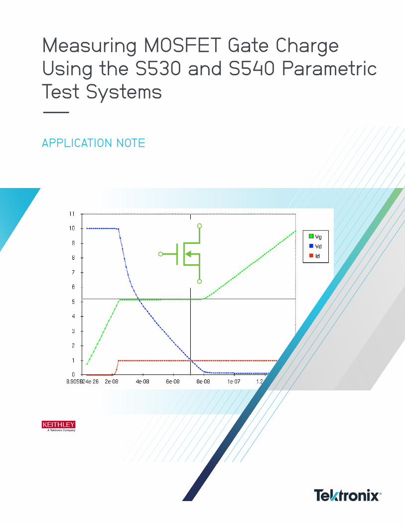
Graphing the Results
If results plotting is enabled, the gate charge waveform will
appear in the KCAT (Keithley Curve Analysis Tool) window
(Figure 7). In this graph, the gate voltage (Vg), drain voltage
(Vd), and the drain current (Id) are plotted as a function of
the gate charge. These parameters can also be plotted as a
function of time.
Table 2. Output Parameters for gate_charge test.
Output Parameter Description
gate_charge Test status values – see Table 3 for descriptions
timeArray Measured time (seconds)
VgArray Measured gate-source voltage (volts)
VgCharge Measured gate charge (coulombs)
VdArray Measured drain voltage (volts)
IdArray Measured drain current (amps)
Slope Dynamic slope (dVg/dt) of gate voltage
Ceff Ratio of gate charge to maximum gate voltage
Vpl Plateau or Miller voltage (volts)
T1 Timestamp where the plateau area begins (seconds)
T2 Timestamp where the plateau area ends (seconds)
Qgs Gate charge from the origin to the first inflection point, or the voltage plateau (coulombs)
Qgd Gate charge between the two inflection points in the gate charge curve (coulombs)
Qg Gate charge from the origin to VgsMax (coulombs)
Figure 7. Typical gate charge waveform of a power transistor.
6 | WWW.TEK.COM
Measuring MOSFET Gate Charge Using the S530 and S540 Parametric Test Systems APPLICATION NOTE

Checking the Test Status
Each time the test is executed,s a test status is returned to the KITT Results
table. Table 3 lists the returned Test Status Values and their corresponding
descriptions and notes.
Table 3. Test Status Values.
Test Status Description Notes
1 No errors Test successful.
–1 Gate Pin is not present Specify correct pin.
–2 Drain Pin is not present Specify correct pin.
–3 VgsMax > 200V Verifies gate voltage is less than 200V. Reduce gate voltage.
–4 Drain current limit exceeds 1 A Verifies drain current is less than 1 A. Reduce drain current limit (drainLimitI).
–5 Power limit exceeded Current should be < 0.1 A if V >20 V. Decrease drain current limit (drainLimitI) or drain voltage (Vds).
–6 Error check on input conditions. Limits timeOut to 300 s.
Specify timeOut to <300 s.
–7 Test time exceeds specified time out (timeOut).
Increase timeOut. Maximum is 300 s. Try increasing gateCurrent to charge up device faster.
–8 Number of iterations/measurements >10000.
Increase gate current (gateCurrent).
–9 Number of iterations/measurements <5
Decrease gate current (gateCurrent). Check device, test set-up and for correct SMU.This error can be ignored if it occurs while measuring an open circuit for offset correction. The Ceff value is still valid.
–10 Number of points from origin to first plateau point is <10
Decrease gate current (gateCurrent)
–11 Error calculating slope, S1. Correlation factor < 0.9. Curve from origin to first plateau point is not linear.
Check device and test set-up.
–12 Error calculating slope, S2. Correlation factor <0.9. Curve from last plateau point to VgsMax is not linear.
Check device and test set-up. If VgCharge or VdArray appear high, try reducing gateCurrent and repeat test.This error can be ignored if it occurs while measuring an open circuit for offset correction. The Ceff value is still valid.
–13 Vds > 200 V Decrease drain voltage.
–14 gateCurrent > 10 µA Decrease gate current (Ig).
ConclusionS530/S540 Parametric Test Systems support
making gate charge measurements on
transistors. Using two SMUs connected
to the gate and drain of the device allows
the KTE software to derive gate charge
waveforms easily.
WWW.TEK.COM | 7
Measuring MOSFET Gate Charge Using the S530 and S540 Parametric Test Systems APPLICATION NOTE

Contact Information
Australia* 1 800 709 465
Austria 00800 2255 4835
Balkans, Israel, South Africa and other ISE Countries +41 52 675 3777
Belgium* 00800 2255 4835
Brazil +55 (11) 3759 7627
Canada 1 800 833 9200
Central East Europe / Baltics +41 52 675 3777
Central Europe / Greece +41 52 675 3777
Denmark +45 80 88 1401
Finland +41 52 675 3777
France* 00800 2255 4835
Germany* 00800 2255 4835
Hong Kong 400 820 5835
India 000 800 650 1835
Indonesia 007 803 601 5249
Italy 00800 2255 4835
Japan 81 (3) 6714 3086
Luxembourg +41 52 675 3777
Malaysia 1 800 22 55835
Mexico, Central/South America and Caribbean 52 (55) 56 04 50 90
Middle East, Asia, and North Africa +41 52 675 3777
The Netherlands* 00800 2255 4835
New Zealand 0800 800 238
Norway 800 16098
People’s Republic of China 400 820 5835
Philippines 1 800 1601 0077
Poland +41 52 675 3777
Portugal 80 08 12370
Republic of Korea +82 2 6917 5000
Russia / CIS +7 (495) 6647564
Singapore 800 6011 473
South Africa +41 52 675 3777
Spain* 00800 2255 4835
Sweden* 00800 2255 4835
Switzerland* 00800 2255 4835
Taiwan 886 (2) 2656 6688
Thailand 1 800 011 931
United Kingdom / Ireland* 00800 2255 4835
USA 1 800 833 9200
Vietnam 12060128
* European toll-free number.
If not accessible, call: +41 52 675 3777
Rev. 090617
Find more valuable resources at TEK.COMCopyright © Tektronix. All rights reserved. Tektronix products are covered by U.S. and foreign patents, issued and pending. Information in this publication supersedes that in all previously published material. Specification and price change privileges reserved. TEKTRONIX and TEK are registered trademarks of Tektronix, Inc. All other trade names referenced are the service marks, trademarks or registered trademarks of their respective companies.
042618.SBG 1KW-61389-0