
Measurements of RF noise in InGaAs/InAlAs recessed diodes...
17
Measurements of RF noise in InGaAs/InAlAs recessed diodes: Signatures of shot-noise suppression 1 O. García-Pérez, J. Mateos, S. Pérez, T. González A. Westlund, J. Grahn
Transcript of Measurements of RF noise in InGaAs/InAlAs recessed diodes...
Measurements of RF noise in InGaAs/InAlAs recessed diodes:
Signatures of shot-noise suppression
1
O. García-Pérez, J. Mateos, S. Pérez, T. González A. Westlund, J. Grahn
2
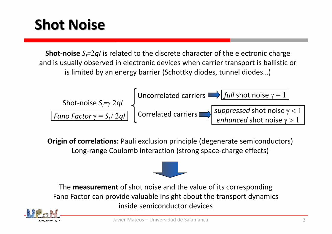
Shot Noise
Uncorrelated carriers
Correlated carriers Shot-noise SI=qI
full shot noise = 1
suppressed shot noise 1enhanced shot noise 1
Origin of correlations: Pauli exclusion principle (degenerate semiconductors) Long-range Coulomb interaction (strong space-charge effects)
Fano Factor = SI qI
The measurement of shot noise and the value of its corresponding Fano Factor can provide valuable insight about the transport dynamics
inside semiconductor devices
Shot-noise SI=qI is related to the discrete character of the electronic charge and is usually observed in electronic devices when carrier transport is ballistic or
is limited by an energy barrier (Schottky diodes, tunnel diodes…)
Javier Mateos – Universidad de Salamanca
Shot Noise
x / L0.0 0.2 0.4 0.6 0.8 1.0
Pote
ntia
l (K
BT/
q)
-5
0
5
10
15 qU/KBT
4020
10
4
0
80
nc nc
thermalequilibrium
thermalequilibrium
x=L
N
x=0
Active region
Contact 1 Contact 2
UPoissonian
injectionPoissonian
injection
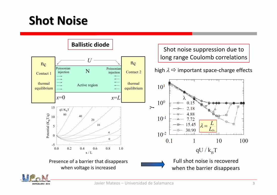
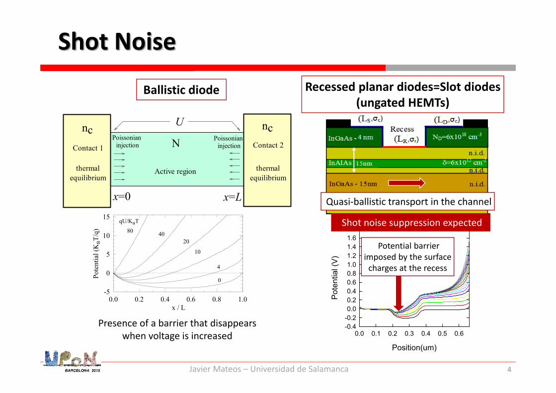
Ballistic diodeShot noise suppression due to
long range Coulomb correlations
high important space-charge effects
DcLL
Full shot noise is recovered when the barrier disappears
Presence of a barrier that disappears when voltage is increased
3Javier Mateos – Universidad de Salamanca
4
x / L0.0 0.2 0.4 0.6 0.8 1.0
Pote
ntia
l (K
BT/
q)
-5
0
5
10
15 qU/KBT
4020
10
4
0
80
nc nc
thermalequilibrium
thermalequilibrium
x=L
N
x=0
Active region
Contact 1 Contact 2
UPoissonian
injectionPoissonian
injection
Position(um)
0.0 0.1 0.2 0.3 0.4 0.5 0.6P
oten
tial (
V)
-0.4-0.20.00.20.40.60.81.01.21.41.61.8
Ballistic diode
Presence of a barrier that disappears when voltage is increased
Shot NoiseRecessed planar diodes=Slot diodes
(ungated HEMTs)
Shot noise suppression expected
Quasi-ballistic transport in the channel
Potential barrier imposed by the surface
charges at the recess
Javier Mateos – Universidad de Salamanca
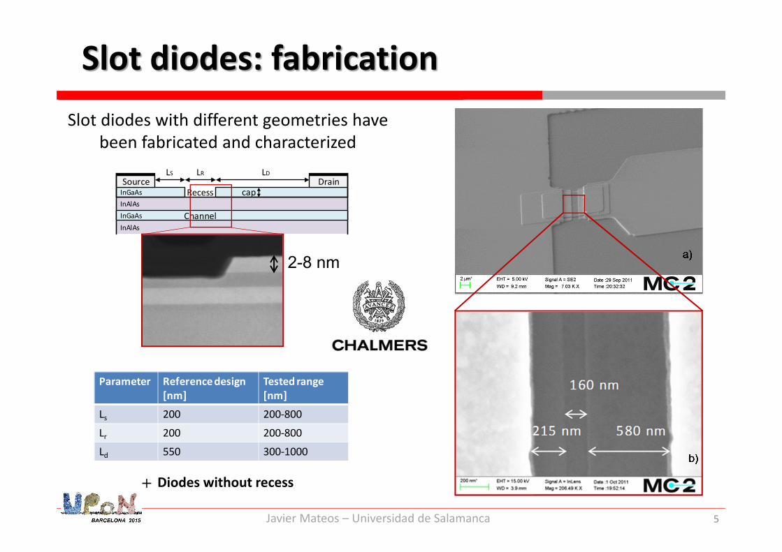
Source DrainRecess
LRLS LD
capInGaAs
InGaAsInAlAs
InAlAsChannel
5
Slot diodes: fabrication
Parameter Reference design [nm]
Tested range [nm]
Ls 200 200-800
Lr 200 200-800
Ld 550 300-1000
Slot diodes with different geometries have been fabricated and characterized
2-8 nm
Diodes without recess+
Javier Mateos – Universidad de Salamanca
6
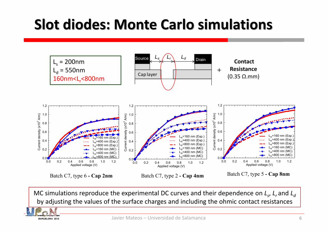
Slot diodes: Monte Carlo simulations
Cap layer
Source DrainLs Lr Ld
Applied voltage (V)0.0 0.2 0.4 0.6 0.8 1.0 1.2
Cur
rent
den
sity
(x10
3 A/m
)
0.0
0.2
0.4
0.6
0.8
1.0
1.2
LR=160 nm (Exp.)LR=400 nm (Exp.)LR=800 nm (Exp.)LR=160 nm (MC)LR=400 nm (MC)LR=800 nm (MC)
Applied voltage (V)0.0 0.2 0.4 0.6 0.8 1.0 1.2
Cur
rent
den
sity
(x10
3 A/m
)
0.0
0.2
0.4
0.6
0.8
1.0
1.2
LR=160 nm (Exp.)LR=400 nm (Exp.)LR=800 nm (Exp.)LR=160 nm (MC)LR=400 nm (MC)LR=800 nm (MC)
Batch C7, type 6 - Cap 2nm
Applied voltage (V)0.0 0.2 0.4 0.6 0.8 1.0 1.2
Cur
rent
den
sity
(x10
3 A/m
)
0.0
0.2
0.4
0.6
0.8
1.0
1.2
LR=160 nm (Exp.)LR=400 nm (Exp.)LR=800 nm (Exp.)LR=160 nm (MC)LR=400 nm (MC)LR=800 nm (MC)
Batch C7, type 2 - Cap 4nm Batch C7, type 5 - Cap 8nm
Ls = 200nmLd = 550nm160nm<Lr<800nm
Contact Resistance
(0.35 Ω.mm)+
MC simulations reproduce the experimental DC curves and their dependence on Ls, Lr and Ldby adjusting the values of the surface charges and including the ohmic contact resistances
Javier Mateos – Universidad de Salamanca
7
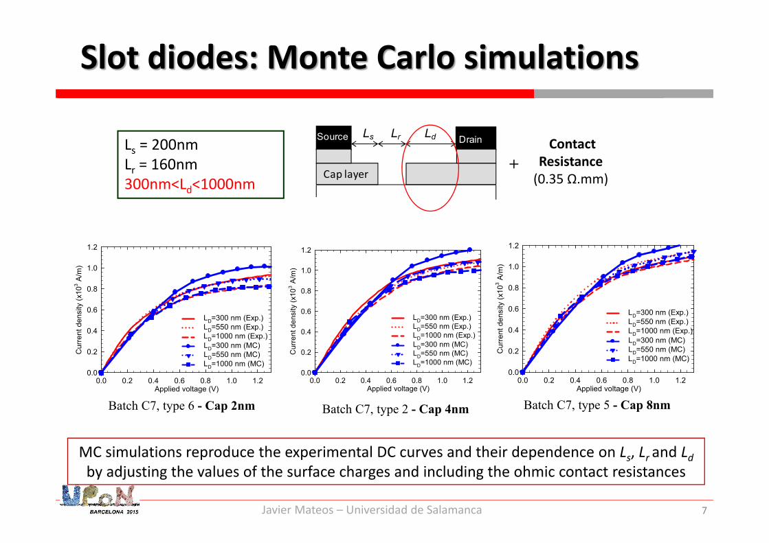
MC simulations reproduce the experimental DC curves and their dependence on Ls, Lr and Ldby adjusting the values of the surface charges and including the ohmic contact resistances
Cap layer
Source DrainLs Lr Ld Contact Resistance
(0.35 Ω.mm)+
Ls = 200nmLr = 160nm300nm<Ld<1000nm
Applied voltage (V)0.0 0.2 0.4 0.6 0.8 1.0 1.2
Cur
rent
den
sity
(x10
3 A/m
)
0.0
0.2
0.4
0.6
0.8
1.0
1.2
LD=300 nm (Exp.)LD=550 nm (Exp.)LD=1000 nm (Exp.)LD=300 nm (MC)LD=550 nm (MC)LD=1000 nm (MC)
Applied voltage (V)0.0 0.2 0.4 0.6 0.8 1.0 1.2
Cur
rent
den
sity
(x10
3 A/m
)
0.0
0.2
0.4
0.6
0.8
1.0
1.2
LD=300 nm (Exp.)LD=550 nm (Exp.)LD=1000 nm (Exp.)LD=300 nm (MC)LD=550 nm (MC)LD=1000 nm (MC)
Applied voltage (V)0.0 0.2 0.4 0.6 0.8 1.0 1.2
Cur
rent
den
sity
(x10
3 A/m
)
0.0
0.2
0.4
0.6
0.8
1.0
1.2
LD=300 nm (Exp.)LD=550 nm (Exp.)LD=1000 nm (Exp.)LD=300 nm (MC)LD=550 nm (MC)LD=1000 nm (MC)
Batch C7, type 6 - Cap 2nm Batch C7, type 2 - Cap 4nm Batch C7, type 5 - Cap 8nm
Slot diodes: Monte Carlo simulations
Javier Mateos – Universidad de Salamanca
8
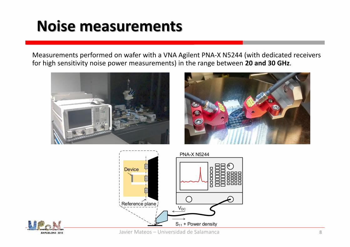
Noise measurements
Reference plane
Device
PNA-X N5244
VDC
S11 + Power density
Measurements performed on wafer with a VNA Agilent PNA-X N5244 (with dedicated receivers for high sensitivity noise power measurements) in the range between 20 and 30 GHz.
Javier Mateos – Universidad de Salamanca
9
Noise measurements
Voltage (V)0.0 0.2 0.4 0.6 0.8 1.0 1.2 1.4
Cur
rent
(mA
)
0
5
10
15
20LD=300nmLD=550nmLD=1000nmNo recess (1300nm)
Current (mA)0 2 4 6 8 10 12 14 16
SI(x
10-2
1 A2 /H
z)0.0
0.5
1.0
1.5
2.0
2.5
3.0
LD=300nmLD=550nmLD=1000nmNo recess (1300nm)2qI
Voltage (V)0.0 0.2 0.4 0.6 0.8 1.0 1.2 1.4
Fano
Fac
tor
0.1
1
10
LD=300nmLD=550nmLD=1000nmNo recess (1300nm)
Voltage (V)0.0 0.2 0.4 0.6 0.8 1.0 1.2 1.4
Cur
rent
(mA
)
0
5
10
15
20LR=160nmLR=400nmLR=800nmNo recess (1300nm)
Current (mA)0 2 4 6 8 10 12 14 16
SI (
x10-2
1 A2 /H
z)
0.0
0.5
1.0
1.5
2.0
2.5
3.0
LR=160nmLR=400nmLR=800nmNo recess (1300nm)2qI
Voltage (V)0.0 0.2 0.4 0.6 0.8 1.0 1.2 1.4
Fano
Fac
tor
0.1
1
10
LR=160nm
LR=400nmLR=800nmNo recess (1300nm)
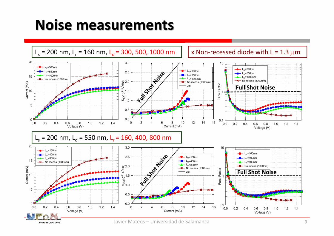
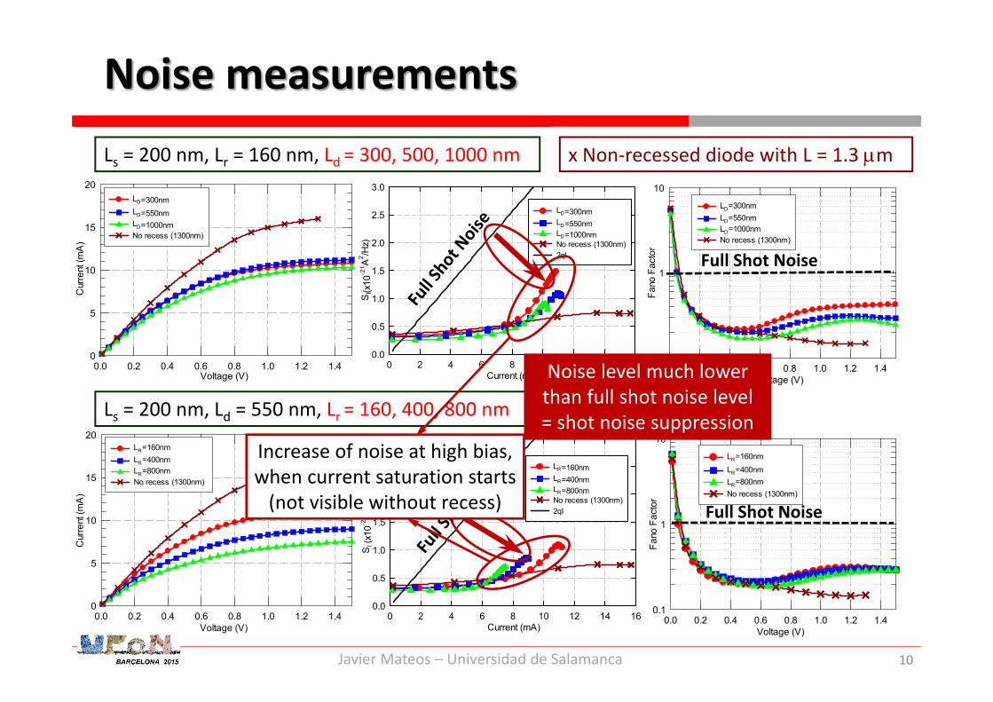
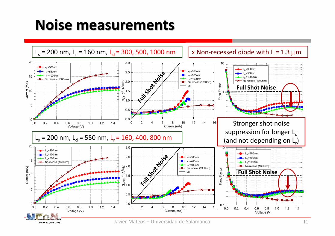
Ls = 200 nm, Lr = 160 nm, Ld = 300, 500, 1000 nm
Ls = 200 nm, Ld = 550 nm, Lr = 160, 400, 800 nm
x Non-recessed diode with L = 1.3 m
Full Shot Noise
Full Shot Noise
Javier Mateos – Universidad de Salamanca
10
Noise measurements
Voltage (V)0.0 0.2 0.4 0.6 0.8 1.0 1.2 1.4
Cur
rent
(mA
)
0
5
10
15
20LD=300nmLD=550nmLD=1000nmNo recess (1300nm)
Current (mA)0 2 4 6 8 10 12 14 16
SI(x
10-2
1 A2 /H
z)0.0
0.5
1.0
1.5
2.0
2.5
3.0
LD=300nmLD=550nmLD=1000nmNo recess (1300nm)2qI
Voltage (V)0.0 0.2 0.4 0.6 0.8 1.0 1.2 1.4
Fano
Fac
tor
0.1
1
10
LD=300nmLD=550nmLD=1000nmNo recess (1300nm)
Voltage (V)0.0 0.2 0.4 0.6 0.8 1.0 1.2 1.4
Cur
rent
(mA
)
0
5
10
15
20LR=160nmLR=400nmLR=800nmNo recess (1300nm)
Current (mA)0 2 4 6 8 10 12 14 16
SI (
x10-2
1 A2 /H
z)
0.0
0.5
1.0
1.5
2.0
2.5
3.0
LR=160nmLR=400nmLR=800nmNo recess (1300nm)2qI
Voltage (V)0.0 0.2 0.4 0.6 0.8 1.0 1.2 1.4
Fano
Fac
tor
0.1
1
10
LR=160nm
LR=400nmLR=800nmNo recess (1300nm)
Ls = 200 nm, Lr = 160 nm, Ld = 300, 500, 1000 nm
Ls = 200 nm, Ld = 550 nm, Lr = 160, 400, 800 nm
x Non-recessed diode with L = 1.3 m
Noise level much lower than full shot noise level = shot noise suppression
Increase of noise at high bias, when current saturation starts
(not visible without recess)
Full Shot Noise
Full Shot Noise
Javier Mateos – Universidad de Salamanca
11
Noise measurements
Voltage (V)0.0 0.2 0.4 0.6 0.8 1.0 1.2 1.4
Cur
rent
(mA
)
0
5
10
15
20LD=300nmLD=550nmLD=1000nmNo recess (1300nm)
Current (mA)0 2 4 6 8 10 12 14 16
SI(x
10-2
1 A2 /H
z)0.0
0.5
1.0
1.5
2.0
2.5
3.0
LD=300nmLD=550nmLD=1000nmNo recess (1300nm)2qI
Voltage (V)0.0 0.2 0.4 0.6 0.8 1.0 1.2 1.4
Fano
Fac
tor
0.1
1
10
LD=300nmLD=550nmLD=1000nmNo recess (1300nm)
Voltage (V)0.0 0.2 0.4 0.6 0.8 1.0 1.2 1.4
Cur
rent
(mA
)
0
5
10
15
20LR=160nmLR=400nmLR=800nmNo recess (1300nm)
Current (mA)0 2 4 6 8 10 12 14 16
SI (
x10-2
1 A2 /H
z)
0.0
0.5
1.0
1.5
2.0
2.5
3.0
LR=160nmLR=400nmLR=800nmNo recess (1300nm)2qI
Voltage (V)0.0 0.2 0.4 0.6 0.8 1.0 1.2 1.4
Fano
Fac
tor
0.1
1
10
LR=160nm
LR=400nmLR=800nmNo recess (1300nm)
Ls = 200 nm, Lr = 160 nm, Ld = 300, 500, 1000 nm
Ls = 200 nm, Ld = 550 nm, Lr = 160, 400, 800 nm
x Non-recessed diode with L = 1.3 m
Stronger shot noise suppression for longer Ld(and not depending on Lr)
Full Shot Noise
Full Shot Noise
Javier Mateos – Universidad de Salamanca
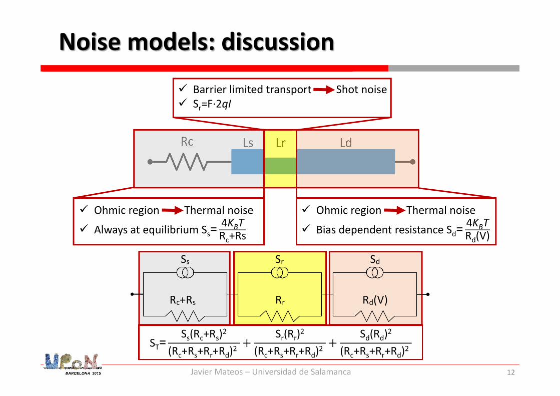
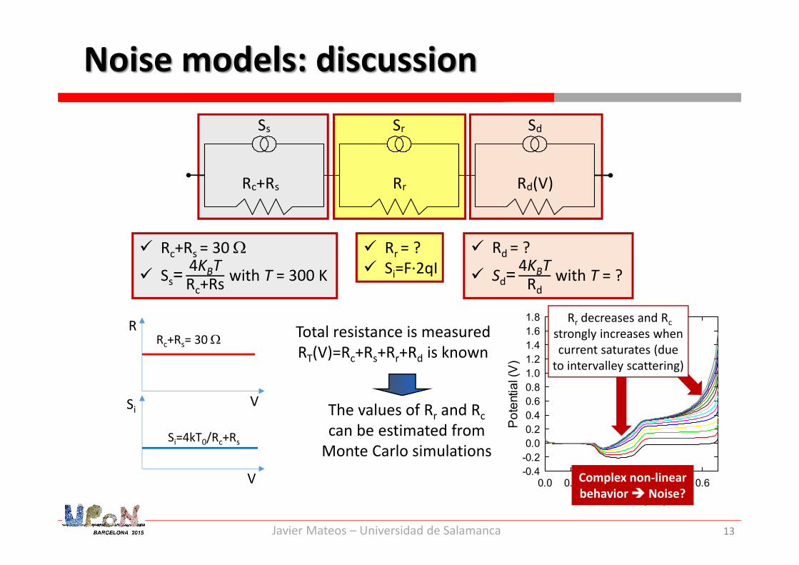
Noise models: discussion
Rc Ls Lr Ld
Ohmic region Thermal noise
Always at equilibrium Ss=4KBTRc+Rs
Ohmic region Thermal noise
Bias dependent resistance Sd=4KBTRd(V)
Barrier limited transport Shot noise Sr=F·2qI
Rc+Rs
Sr Ss Sd
Rr Rd(V)
12Javier Mateos – Universidad de Salamanca
Position(um)0.0 0.1 0.2 0.3 0.4 0.5 0.6
Pot
entia
l (V
)
-0.4-0.20.00.20.40.60.81.01.21.41.61.8
Noise models: discussion
Rc+Rs = 30
Ss=4KBTRc+Rs with T = 300 K
Rr = ? Si=F·2qI
Rd = ?
Sd=4KBT
Rdwith T = ?
Rc+Rs= 30 R
V
V
Si
Si=4kT0/Rc+Rs
Rc+Rs
Sr Ss Sd
Rr Rd(V)
Total resistance is measured RT(V)=Rc+Rs+Rr+Rd is known
The values of Rr and Rc can be estimated from
Monte Carlo simulations
Rr decreases and Rcstrongly increases when current saturates (due
to intervalley scattering)
Complex non-linear behavior Noise?
13Javier Mateos – Universidad de Salamanca
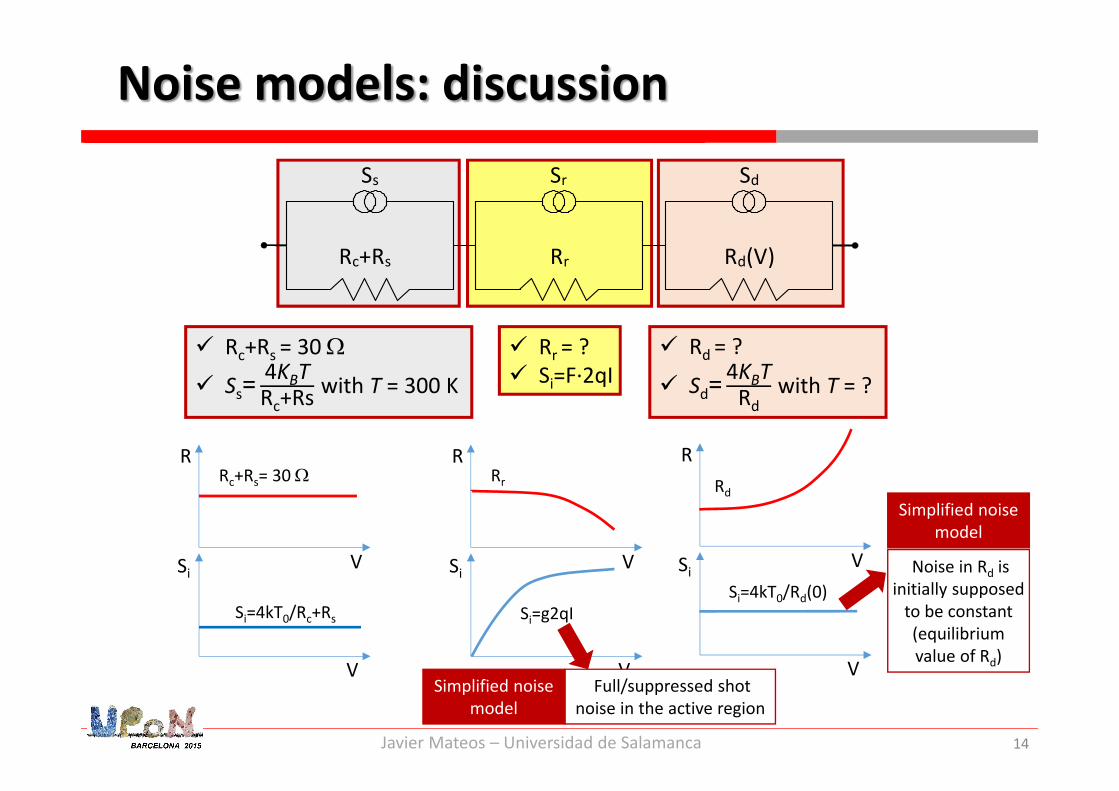
Noise models: discussion
Rc+Rs
Sr Ss Sd
Rr Rd(V)
Rr
R
V
V
Si
Si=g2qI
Rd
R
V
V
SiSi=4kT0/Rd(0)
Noise in Rd is initially supposed
to be constant (equilibrium value of Rd)
Rc+Rs = 30
Ss=4KBTRc+Rs with T = 300 K
Rr = ? Si=F·2qI
Rd = ?
Sd=4KBT
Rdwith T = ?
Rc+Rs= 30 R
V
V
Si
Si=4kT0/Rc+Rs
Simplified noise model
14
Full/suppressed shot noise in the active region
Simplified noise model
Javier Mateos – Universidad de Salamanca
Voltage (V)0.0 0.2 0.4 0.6 0.8 1.0 1.2 1.4
Fano
Fac
tor
0.1
1
10
LR=160nmLR=400nmLR=800nm
Model Exp.
Current (mA)0 2 4 6 8 10 12
SI (
10-2
1 A
2 /Hz)
0.0
0.5
1.0
1.5
2.0
Voltage (V)0.0 0.2 0.4 0.6 0.8 1.0 1.2 1.4
Fano
Fac
tor
0.1
1
10
LD=300nmLD=550nmLD=1000nm
Model Exp.
Current (mA)0 2 4 6 8 10 12
SI(1
0-21
A2 /H
z)
0.0
0.5
1.0
1.5
2.0
15
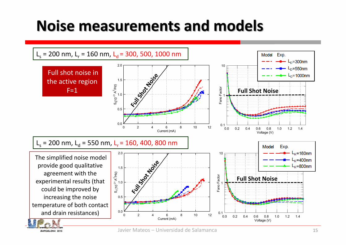
Noise measurements and models
LD=300nmLD=550nmLD=1000nm
Model Exp.
Current (mA)0 2 4 6 8 10 12
SI(1
0-21
A2 /H
z)
0.0
0.5
1.0
1.5
2.0
Voltage (V)0.0 0.2 0.4 0.6 0.8 1.0 1.2 1.4
Fano
Fac
tor
0.1
1
10
LR=160nmLR=400nmLR=800nm
Model Exp.
Current (mA)0 2 4 6 8 10 12
SI (
10-2
1 A
2 /Hz)
0.0
0.5
1.0
1.5
2.0
Voltage (V)0.0 0.2 0.4 0.6 0.8 1.0 1.2 1.4
Fano
Fac
tor
0.1
1
10
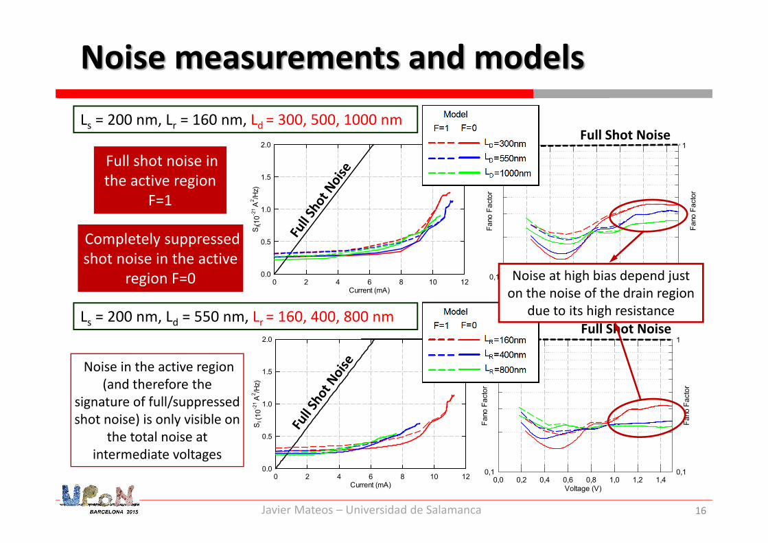
Ls = 200 nm, Lr = 160 nm, Ld = 300, 500, 1000 nm
Ls = 200 nm, Ld = 550 nm, Lr = 160, 400, 800 nm
Full Shot Noise
Full Shot Noise
Full shot noise in the active region
F=1
The simplified noise model provide good qualitative
agreement with the experimental results (that
could be improved by increasing the noise
temperature of both contact and drain resistances)
Javier Mateos – Universidad de Salamanca
Voltage (V)0,0 0,2 0,4 0,6 0,8 1,0 1,2 1,4
Fano
Fac
tor
0,1
1
Voltage (V)0,0 0,2 0,4 0,6 0,8 1,0 1,2 1,4
Fano
Fac
tor
0,1
1
Fano
Fac
tor
0,1
1
Voltage (V)0.0 0.2 0.4 0.6 0.8 1.0 1.2 1.4
Fano
Fac
tor
0.1
1
Voltage (V)0,0 0,2 0,4 0,6 0,8 1,0 1,2 1,4
Fano
Fac
tor
0,1
1
Fano
Fac
tor
0,1
1
LD=300nmLD=550nmLD=1000nm
Model Exp.
Current (mA)0 2 4 6 8 10 12
SI(1
0-21
A2 /H
z)
0.0
0.5
1.0
1.5
2.0
LR=160nmLR=400nmLR=800nm
Model Exp.
Current (mA)0 2 4 6 8 10 12
SI (
10-2
1 A
2 /Hz)
0.0
0.5
1.0
1.5
2.0
LR=160nmLR=400nmLR=800nm
Model Exp.
Current (mA)0 2 4 6 8 10 12
SI (
10-2
1 A
2 /Hz)
0.0
0.5
1.0
1.5
2.0
LD=300nmLD=550nmLD=1000nm
Model Exp.
Current (mA)0 2 4 6 8 10 12
SI(1
0-21
A2 /H
z)
0.0
0.5
1.0
1.5
2.0
16
Noise measurements and modelsLs = 200 nm, Lr = 160 nm, Ld = 300, 500, 1000 nm
Ls = 200 nm, Ld = 550 nm, Lr = 160, 400, 800 nm
Full Shot Noise
Full Shot Noise
Completely suppressed shot noise in the active
region F=0
Full shot noise in the active region
F=1
Noise in the active region (and therefore the
signature of full/suppressed shot noise) is only visible on
the total noise at intermediate voltages
Noise at high bias depend just on the noise of the drain region
due to its high resistance
Javier Mateos – Universidad de Salamanca
• Measurements of noise performed in a set of recessed planar InGaAs/InAlAs diodes with different dimensions show potential signs of shot noise suppression in the structures due to the presence of a potential barrier
• A detailed analysis of the noise contribution of the different regions of the devices shows that contact, source and drain resistances strongly affect the value of the total noise
• The possible shot noise suppression appearing under the recess could just be visible on the total noise at intermediate bias (before the onset of intervalley scattering) where the resistance of the drain region is still low
• Devices with reduced access and drain resistances should be fabricated in order to obtain conclusive results
17
Conclusions
Javier Mateos – Universidad de Salamanca
![LVCSupernovaWorkshopSearchesPanel Mezzacappa V2 · 00.2 0.40.6 0.8 1 1.2 Time from bounce [s] 0 0.2 0.4 0.6 0.8 Explosion Energy [B] W-H 12 solar mass progenitor W-H 15 solar mass](https://static.fdocuments.net/doc/165x107/60548c37d130b540a54813d5/lvcsupernovaworkshopsearchespanel-mezzacappa-v2-002-0406-08-1-12-time-from.jpg)


