![arXiv:1308.1239v1 [cond-mat.mtrl-sci] 6 Aug 2013 · Chemical Mechanical Polishing was performed with a Logitech Tribo polishing system in conjunction with a SUBA-X polishing pad and](https://static.fdocuments.net/doc/165x107/5acaed687f8b9acb7c8e901a/arxiv13081239v1-cond-matmtrl-sci-6-aug-2013-mechanical-polishing-was-performed.jpg)
MEASUREMENT OF PAD COMPRESSION DURING CHEMICAL MECHANICAL POLISHING … · measurement of pad...
126
MEASUREMENT OF PAD COMPRESSION DURING CHEMICAL MECHANICAL POLISHING A Thesis submitted by Caprice Gray IN PARTIAL FULFILLMENT OF THE REQUIREMENTS FOR THE DEGREE OF MASTER OF SCIENCE IN MECHANICAL ENGINEERING TUFTS UNIVERSITY MEDFORD, MA 02155 AUGUST 2005 ADVISOR: CHRIS ROGERS, SC.D
Transcript of MEASUREMENT OF PAD COMPRESSION DURING CHEMICAL MECHANICAL POLISHING … · measurement of pad...

MEASUREMENT OF PAD COMPRESSIONDURING CHEMICAL MECHANICAL
POLISHING
A Thesis submitted by
Caprice Gray
IN PARTIAL FULFILLMENT OF THE REQUIREMENTS FOR THE DEGREE
OF MASTER OF SCIENCE IN MECHANICAL ENGINEERING
TUFTS UNIVERSITYMEDFORD, MA 02155
AUGUST 2005
ADVISOR: CHRIS ROGERS, SC.D

Abstract
In the 1980s, the semiconductor industries started to use Chemical Mechanical Pol-
ishing (CMP) to planarize silicon wafers before patterning integrated circuits (ICs).
At the time, little was known about the physics and chemistry involved in CMP. The
push towards miniaturization in the past few decades has led to a desire for a better
understanding of the CMP mechanism. Many research groups have explored CMP
via modeling and experimentation. Experimentalists have difficulty verifying the
results produced by the modeling because it is difficult to “see” what is happening
under the wafer while polishing. In the mid 1990s, Tufts University in conjunc-
tion with the University of Arizona, Intel Corporation and Cabot Microelectronics
Corporation, began an effort to make in-situ measurements of physical properties
underneath the wafer using a technique called Dual Emission Laser Induced Fluo-
rescence (DELIF).
In this work, the DELIF setup at Tufts has been modified such that we can at-
tain instantaneous images of the slurry layer thickness at high spatial and temporal
resolution during polishing. It is now possible to make measurements at an asperity
scale resolution. In this thesis, I present both qualitative and quantitative obser-
vations of the slurry layer as it passes between the polishing pad a wafer features.
ii

Images were analyzed to determine pad roughness, local pad deformation and as-
perity compression during the polishing of wafers with etched steps. By calculating
a relative calibration factor, it is possible to estimate asperity compression during
polishing. The ability to resolve wafer features is limited by pad topography. This
calibration factor allows us to examine slurry film roughness, slurry layer thickness
changes near steps in the wafer, and asperity compression and expansion under the
wafer. Step steepness and heights can be characterized by fitting the average cross
section across a step to a hyperbolic tangent curve. Global pad topography results
in widely varying fluid displacement due to applied down-forces to the wafer over
small areas (6 mm2). Analysis of asperity compression in static images after apply-
ing 70kPa down-force shows that average asperity compression increases with the
reduction of the average slurry layer thickness. Dynamic measurements show that
asperity expansion increases with well depth.
iii

Acknowlegements
This work would not have been possible without help from many sources. First, I
would like thank our funders, Cabot Microelectronics Corporation and Intel Corpo-
ration. The representatives from these companies include Mansour Moinpour and
Chris Barns from Intel, and Sriram Anjur from Cabot. These people have provided
both excellent intellectual input as well as supplies for our experimental research.
Second, I would also like to thank Professor Ara Philipossian and the students of his
lab at the University of Arizona, Tucson, for their continuing input on this project.
I have many people to thank at Tufts University. First and foremost, I would
like to thank Professors Chris Rogers and Vincent Manno for giving a Chemist the
opportunity to learn a bit of engineering. Second, I would like to thank my partner
in this research, Daniel Apone. Dan has been one of the best research partners I have
ever had and this project definitely would not have been possible without his help. I
would also like to acknowledge the other student working on Tufts CMP while I have
been here, Scott Taylor and Jim Vlahakis for their ideas and input. I would like to
thank two professors from outside the Mechanical Engineering Department, Professor
David Wilbur of the Chemistry Department and Professor Bruce Boghosian in the
iv

Mathematics Department. Professor Wilbur helped me with all the spectroscopy
and Professor Boghosian helped with understanding the image statistics. Finally, I
would like to thank everyone who has been a part of TUFTL for the past couple of
years for making it a wonderful place to work.
Last, but not least, I would like to thank my family for their continuing support
throughout my education. Mom and Dad always made it a priority to put my brother
and I through school. We made it, thanks. Nicky, your an awesome brother, but you
didn’t hear that from me. Thanks to all of my grandparents for the love and support
and snail mail, Peggy, Pete, Rene, 9E - you all are some of the most amazing people
I know.
v
Contents
1 Introduction 1
1.1 IC and Semiconductor Manufacturing . . . . . . . . . . . . . . . . . . 3
1.2 Chemical Mechanical Polishing . . . . . . . . . . . . . . . . . . . . . 5
1.2.1 Recent Experimental Advances . . . . . . . . . . . . . . . . . 5
1.2.2 Recent Advances in Modeling CMP . . . . . . . . . . . . . . . 8
1.3 History of DELIF in CMP . . . . . . . . . . . . . . . . . . . . . . . . 10
1.4 Goals of this Research . . . . . . . . . . . . . . . . . . . . . . . . . . 12
2 Experimental Setup 14
2.1 Polishing Setup Modifications . . . . . . . . . . . . . . . . . . . . . . 19
2.1.1 Force Table . . . . . . . . . . . . . . . . . . . . . . . . . . . . 19
2.1.2 Wafer Rotation . . . . . . . . . . . . . . . . . . . . . . . . . . 19
2.1.3 Conditioning . . . . . . . . . . . . . . . . . . . . . . . . . . . 20
2.2 Dual Emission Laser Induced Fluorescence . . . . . . . . . . . . . . . 23
2.2.1 Theoretical Overview . . . . . . . . . . . . . . . . . . . . . . . 23
2.2.2 Modifications to DELIF Procedure . . . . . . . . . . . . . . . 26
vi

2.3 Optical Setup . . . . . . . . . . . . . . . . . . . . . . . . . . . . . . . 29
2.3.1 Laser . . . . . . . . . . . . . . . . . . . . . . . . . . . . . . . . 29
2.3.2 Pad, Wafer, Slurry . . . . . . . . . . . . . . . . . . . . . . . . 32
2.3.3 Cameras, Lens and Filters . . . . . . . . . . . . . . . . . . . . 32
3 Image Calibration 36
3.1 Wafer Etching . . . . . . . . . . . . . . . . . . . . . . . . . . . . . . . 37
3.2 Calibration . . . . . . . . . . . . . . . . . . . . . . . . . . . . . . . . 38
3.2.1 Previous Calibration Attempts . . . . . . . . . . . . . . . . . . 40
3.2.2 Relative Thickness . . . . . . . . . . . . . . . . . . . . . . . . 41
3.2.3 Absolute Thickness . . . . . . . . . . . . . . . . . . . . . . . . 43
3.3 Experimental Sources of Error . . . . . . . . . . . . . . . . . . . . . . 44
3.3.1 DELIF . . . . . . . . . . . . . . . . . . . . . . . . . . . . . . . 44
3.3.2 Calibration . . . . . . . . . . . . . . . . . . . . . . . . . . . . 50
4 Image Analysis 53
4.1 Qualitative Image Analysis . . . . . . . . . . . . . . . . . . . . . . . . 54
4.1.1 Images of Different Types of Pads . . . . . . . . . . . . . . . . 55
4.1.2 Well Resolution . . . . . . . . . . . . . . . . . . . . . . . . . . 59
4.1.3 Conditioner Marks on Pads . . . . . . . . . . . . . . . . . . . 62
4.1.4 Air Pockets . . . . . . . . . . . . . . . . . . . . . . . . . . . . 66
4.1.5 Pitch Resolution . . . . . . . . . . . . . . . . . . . . . . . . . 68
4.2 Quantitative Image Analysis . . . . . . . . . . . . . . . . . . . . . . . 75
4.2.1 Fruedenberg FX9 Pad Characterization . . . . . . . . . . . . . 76
vii

4.2.2 Surface Roughness . . . . . . . . . . . . . . . . . . . . . . . . 77
4.2.3 Local Step Parameters . . . . . . . . . . . . . . . . . . . . . . 83
4.2.4 Asperity Compression . . . . . . . . . . . . . . . . . . . . . . 90
5 Summary, Conclusions and Future Work 101
5.1 Setup Modifications . . . . . . . . . . . . . . . . . . . . . . . . . . . . 101
5.2 Experimental Conclusions . . . . . . . . . . . . . . . . . . . . . . . . 102
5.3 Future Research Directions . . . . . . . . . . . . . . . . . . . . . . . . 104
viii

List of Figures
1.1 An IC cross section [14]. Multiple planarization step were required to
build this device. . . . . . . . . . . . . . . . . . . . . . . . . . . . . . 4
1.2 A schematic of a typical CMP rotary polishing tool (Image source:
http : //www.ipms.fraunhofer.de/products/ptf/cmpd.shtml) . . . . 6
2.1 Most recent laboratory scale CMP tool design. . . . . . . . . . . . . . 16
2.2 CMP tool used in previous research. . . . . . . . . . . . . . . . . . . 17
2.3 A schematic of the relative pad-wafer rotation motions and the sam-
pling region of interest (ROI). . . . . . . . . . . . . . . . . . . . . . . 18
2.4 Oscillating down-force with rotation of the drill press shaft. . . . . . . 21
2.5 A more constant down-force was observed in the new setup without
the drill press. . . . . . . . . . . . . . . . . . . . . . . . . . . . . . . . 22
2.6 New wafer-shaft coupling. . . . . . . . . . . . . . . . . . . . . . . . . 22
2.7 Schematic of conditioning system . . . . . . . . . . . . . . . . . . . . 24
2.8 Fluorescence emission of dyed and undyed Fruedenberg FX9 polishing
pads. . . . . . . . . . . . . . . . . . . . . . . . . . . . . . . . . . . . . 28
2.9 Spectral characterization of the pad-Calcien DELIF system. . . . . . 30
ix

2.10 Light paths and camera positions with respect to the imaging target. 31
2.11 Light path near the wafer. . . . . . . . . . . . . . . . . . . . . . . . . 33
2.12 Evolution VF cameras used for data acquisition. . . . . . . . . . . . . 34
2.13 Filters and beam-splitter locations. . . . . . . . . . . . . . . . . . . . 35
2.14 Nikon 135mm f/5.6 El-Nikkor enlarging lens . . . . . . . . . . . . . . 35
3.1 Wafer etch pattern and well cross section. Note: the cross section is
not to scale. . . . . . . . . . . . . . . . . . . . . . . . . . . . . . . . . 39
3.2 Image used for x-y pixel calibration . . . . . . . . . . . . . . . . . . . 40
3.3 Previously used calibration techniques (a) Microscope slides with a
shim, (b) Flat wafer over the pad at an angle produced by microscope
slide. . . . . . . . . . . . . . . . . . . . . . . . . . . . . . . . . . . . . 42
3.4 Schematic of the method used to determine the relative thickness cal-
ibration factor. . . . . . . . . . . . . . . . . . . . . . . . . . . . . . . 43
3.5 DELIF components as seen through the Calcein camera. . . . . . . . 47
3.6 DELIF components as seen through the pad camera. . . . . . . . . . 49
3.7 Final ratio of the Calcein camera images divided by the pad camera
images. . . . . . . . . . . . . . . . . . . . . . . . . . . . . . . . . . . . 51
4.1 Pad Grooving (not to scale). The left is an image of an xy-grooved
and thin-grooved pad. The right is an image of a k-grooved pad. . . . 56
4.2 DELIF images of flat Fruedneberg FX9 polishing pads (a) Dyed (b)
undyed . . . . . . . . . . . . . . . . . . . . . . . . . . . . . . . . . . . 57
x

4.3 DELIF images of pads with k-grooves (a) Fruedenberg FX9 (b) Rodel
IC1000 . . . . . . . . . . . . . . . . . . . . . . . . . . . . . . . . . . . 58
4.4 DELIF images of CMC experimental pads (a) Flat CMC M2 (b) thin-
grooved CMC M2 (c) xy-grooved CMC M3 . . . . . . . . . . . . . . . 60
4.5 DELIF image of wafers with etched square wells over the flat, dyed
Fruedenberg FX9 pad (a) 1 mm2, 14.5 µm deep well (b) 1 mm2, 27
µm deep well . . . . . . . . . . . . . . . . . . . . . . . . . . . . . . . 61
4.6 DELIF image of a wafer with 5 µm deep wells on an undyed, flat
Fruedenberg FX9 with sub-pad. (a) original image (b) enhanced image 61
4.7 Well resolution over the Rodel IC1000 k-grooved pad (a) 14.5 µm deep
wells (b) 27 µm deep wells . . . . . . . . . . . . . . . . . . . . . . . . 63
4.8 Well resolution over the Fruedenberg FX9 k-grooved pad (a) 14.5 µm
deep wells (b) 27 µm deep wells . . . . . . . . . . . . . . . . . . . . . 64
4.9 Enhanced images of figures 4.7 and 4.8. . . . . . . . . . . . . . . . . . 64
4.10 Pad striations caused by the conditioner on a flat Fruedenberg FX9
polishing pad under (a) a flat wafer (b) 14.5 µm deep wells . . . . . . 65
4.11 Air pockets under 27 µm deep wells on a Fruedenberg FX9 pad (a)
Middle of well (b) Trailing edge of well (c) Air dissipating from inside
to outside the well . . . . . . . . . . . . . . . . . . . . . . . . . . . . 67
4.12 The air pockets are confined to the grooves under the 27 µm deep
wells (a) Rodel IC1000 k-grooved pad (b) Fruedenberg FX9 k-grooved
pad . . . . . . . . . . . . . . . . . . . . . . . . . . . . . . . . . . . . . 69
4.13 Microscope image of a wafer etched trenches of different depths . . . 70
xi
4.14 3D DELIF image of a wafer with multiple step heights over a flat
Fruedenberg FX9 polishing pad . . . . . . . . . . . . . . . . . . . . . 72
4.15 Average cross section over deep trenches . . . . . . . . . . . . . . . . 73
4.16 Average Cross section over shallow trenches . . . . . . . . . . . . . . 74
4.17 Schematic of trench averaging . . . . . . . . . . . . . . . . . . . . . . 76
4.18 Profilometer scan of a Fruedenberg FX9 polishing pad. The imaged
region is magnified in the inlay. . . . . . . . . . . . . . . . . . . . . . 78
4.19 A cartoon of asperity expansion under the well regions . . . . . . . . 79
4.20 The roughness values inside the well are greater than roughness out-
side the well . . . . . . . . . . . . . . . . . . . . . . . . . . . . . . . . 81
4.21 Histograms of roughness values inside and outside well regions . . . . 82
4.22 Surface roughness with increasing down-force during polishing . . . . 84
4.23 A comparison of roughness inside and outside the wells and under-
neath air pockets . . . . . . . . . . . . . . . . . . . . . . . . . . . . . 85
4.24 A DELIF cross section across a wafer step . . . . . . . . . . . . . . . 86
4.25 Average cross section across two 27 µm deep wells on a Fruedenberg
FX9 pad . . . . . . . . . . . . . . . . . . . . . . . . . . . . . . . . . . 87
4.26 Average cross-section across a single wafer step 14.5 µm deep . . . . . 88
4.27 An average cross section of a step fit to a sloped hyperbolic tangent
curve . . . . . . . . . . . . . . . . . . . . . . . . . . . . . . . . . . . . 89
4.28 Step fit parameters a (steepness) and b (step height) normalized to
the values of the 27 µm deep wafer . . . . . . . . . . . . . . . . . . . 91
xii

4.29 Pad-wafer slope tracking (parameter c) over runs with different wafer
step heights . . . . . . . . . . . . . . . . . . . . . . . . . . . . . . . . 92
4.30 Histograms of DELIF intensities for a compressed and uncompressed
pad . . . . . . . . . . . . . . . . . . . . . . . . . . . . . . . . . . . . . 95
4.31 A comparison of the mean fluid thickness difference compared to as-
perity compression under 70 kPa down-force . . . . . . . . . . . . . . 96
4.32 Sub-images used to examine asperity compression and expansion near
wafer steps . . . . . . . . . . . . . . . . . . . . . . . . . . . . . . . . . 96
4.33 A comparison of standard deviations of intensity inside and outside
well regions for the 14.5 µm and 27 µm deep wells . . . . . . . . . . . 98
4.34 Asperity compression from inside to outside the 3 different well depths
compared to the mean fluid height difference . . . . . . . . . . . . . . 100
xiii

List of Tables
2.1 A list of experiments performed and the experimental setup used . . . 15
2.2 Possible decay pathways for an electron in its excited state . . . . . . 26
4.1 Average value of asperity height, σ, and errors for dynamic image in
regions 1 (R1) and 2 (R2) . . . . . . . . . . . . . . . . . . . . . . . . 97
xiv

Chapter 1
Introduction
Chemical Mechanical Polishing (CMP), also known as Chemical Mechanical Pla-
narization, is a technique that has been used for thousands of years to polish glass
surfaces such as mirrors [1]. In the 1980s, the semiconductor industries started to use
CMP to polish silicon wafers before patterning integrated circuits (ICs) [2]. At the
time, little was known about the physics and chemistry involved in CMP. However,
the process worked well, and was integrated into the microchip manufacturing pro-
cess. The push towards miniaturization in the past few decades has led to a desire
for better understanding of the CMP mechanisms [3].
The majority of the experimental research done to determine what is happening
to the wafer, pad and slurry involves polishing, then examining the wafer or pad
ex-situ. To gain a deeper understanding of the pad-slurry-wafer interactions, many
research groups have focused their efforts on simulations and modeling CMP tribol-
ogy [4, 5, 6, 7]. Modeling CMP has proven to be extraordinarily difficult due to
1

the plethora of variables involved in the process. Experimental verification of the
models often involves ex-situ [4, 5] observations or indirect observations in-situ [8].
Experimentalists have had difficulty verifying the results produced by the modeling
because it is difficult to “see” exactly what is happening under the wafer during
polishing.
About a decade ago, Tufts University in conjunction with the University of Ari-
zona, Intel Corporation and Cabot Microelectronics Corporation, began an effort to
make in-situ measurements of physical properties underneath the wafer [9]. The sili-
con wafer and its carrier were replaced by an optically transparent glass wafer. With
the use of high resolution cameras, specialized fluorescent dyes, and UV light, it was
possible to attain in-situ measurements of temperature, pH, and average slurry film
thickness. This imaging process is called Dual Emission Laser Induced Fluorescence
(DELIF) [10].
In this thesis, the DELIF setup has been modified such that we can attain instan-
taneous images of the slurry layer thickness at high spatial and temporal resolution
during polishing. It is now possible to make measurements at pad asperity scale
resolution. In this thesis, I present both qualitative and quantitative observations of
the slurry layer as it passes between the polishing pad and wafer features. Images
were analyzed to determine pad roughness, local pad deformation and asperity com-
pression during the polishing of wafers with etched steps. Finally, future directions
for this research will be presented. We plan ultimately to compare this experimental
data with modeling efforts both at Tufts University and other research institutions.
Once the accuracy of CMP models is verified by experiments, the models can then
2

be used to improve industrial CMP.
1.1 IC and Semiconductor Manufacturing
CMP has proven to be a most useful tool in the manufacturing of integrated circuits
(ICs) and micro electro-mechanical devices (MEMs) over the past several decades.
Device manufacturing is a multi-step process that involves alternating material pat-
terning processes and planarization techniques [11]. For example, the following are
the steps that might be used to fabricate an interconnection:
1. Deposition of dielectric layer
2. Photolithography
3. Etch vias and trenches
4. CVD (Chemical Vapor Deposition) or sputtering of via metal
5. CMP to patterned metal
Most state-of-the-art IC features are now much smaller than 100 nm and many
MEMs features are now manufactured in the 1-100 µm range [12]. As feature sizes
decrease below 100 nm, the number of design rules required to manufacture the
IC increase exponentially [13]. Figure 1.1 shows a cross section of an IC chip [14].
There are 5 or more planarization step required to produce this device. Not all
planarization is done with CMP, but CMP is one of the most common techniques.
Due to the number of variables involve in the CMP process, it is difficult to optimize
planarization and ultimately the device design and manufacturing process.
3

Figure 1.1: An IC cross section [14]. Multiple planarization step were required tobuild this device.
4

1.2 Chemical Mechanical Polishing
CMP is used to planarize both metal and dielectric layers. In both processes the
CMP tool is similar in design, however the chemical and mechanical processes in-
volved in metal planarization are quite different from those involved in dielectric
planarization. Figure 1.2 depicts a basic CMP tool. The CMP tool typically consists
of a polishing pad, slurry injection system and a wafer carrier. The wafer is rotated
in the same direction as the polishing pad. For silicon polishing, which is the focus
of this thesis, a slurry containing colloidal silica abrasive is buffered at a high pH
and reacts chemically with the oxide surface during polishing. The outermost layer
of the oxide surface becomes soft and is gently mechanically abraded by the slurry
particles and the polishing pad [1].
1.2.1 Recent Experimental Advances
Much of the most recent experimental work that has been done to determine CMP
polishing mechanisms in-situ has focused on coefficient of friction (COF) measure-
ments. It has been proven that there is a linear relationship between removal rate
and COF during oxide polishing [15, 16]. Spectral decomposition of the COF in
time will hopefully reveal individual parameters that contribute to the wafer stick-
slip phenomena that is believed to be partially responsible for oxide removal. Friction
measurements have also been used to estimate the degree of pad-slurry particle con-
tact as slurry pH and down force is varied [17] and investigate optimal particle loading
in CMP slurries [18]. Yet another study used the COF to discover that polishing
5

Figure 1.2: A schematic of a typical CMP rotary polishing tool (Image source: http ://www.ipms.fraunhofer.de/products/ptf/cmpd.shtml)
6
pad life is extended when the slurry flow rate is increased [19].
Aside from DELIF, the most common optical technique used to study CMP is
infrared imaging [20, 21, 22]. Since infrared images primarily detect temperature
changes, experiments can be run on the actual silicon wafer as opposed to the opti-
cally transparent disks used for DELIF measurements [21, 22]. Temperature maps
from these infrared camera images have been directly correlated with friction mea-
surements. As expected, temperature increases with applied down force. Kim, et.
al. correlated temperature and friction measurements with pad-wafer contact area
by taking microscope images through a glass wafer pressing on a polishing pad at
different temperatures [22]. This technique is similar to static DELIF imaging. Kim
et. al. found that as temperature increases, asperity hardness decreases leading to
larger pad-wafer contact.
A unique study of removal rate using infrared imaging was done by Ogawa, et.
al. in which infrared spectra were acquired during polishing [23]. In this exper-
imental setup, the silicon wafer was stationary and a polishing pad with a much
smaller diameter than the wafer was rotated over the wafer surface. An IR source
was mounted at 450 to the wafer surface and a detector was mounted opposite the
source at a 450 angle to the wafer. IR spectra were collected over the Si-H stretch
region, the spectral region that corresponds to the Si-H bond oscillation frequency.
Increasing spectral intensity corresponds to increasing surface hydrolysation. The
measurements rate was 1 spectra every 0.32 minutes and was limited by the rate
at which this spectroscopy could be performed. In this way, oxide growth during
polishing was monitored and it was possible to monitor the chemical evolution of the
7

wafer surface at different pressures, pad-wafer speeds, and pHs.
1.2.2 Recent Advances in Modeling CMP
There are two primary reasons why research groups model the CMP process. First,
it is desirable to connect the fundamental laws of physics to what we are observing
experimentally; and second, some phenomena are too difficult to observe experi-
mentally and can only be observed by simulations. Many modeling efforts have
focused on the same topics that will be discussed in this thesis: fluid film thickness
[8], pad compressibility [4] and pad topography near wafer steps [5]. Most models
are based upon Preston’s equation, which relates removal rate to pressure and pad-
wafer velocity [7, 6], solving the Navier-Stokes equations [24], and/or Lubrication
theory [4, 25, 26, 27, 28]. The following paragraphs present some of the most recent
modeling advances and the experiments performed to verify these models.
Ouma, et. al. investigated micron sized step erosion and polishing pad conforma-
tion around that step [5]. When polishing wafer steps, there is typically a high degree
of local planarity after polishing. However, the global topography post polishing is
not as flat. A model was developed to mimic the wafer erosion, which is the material
removal rate during polishing, in time. Experimental verification of the model was
limited to ex-situ metrology of the wafer surface.
Mullany and Byrne developed a thin-film lubrication model based on the Reynolds
Equation to determine a relationship between slurry viscosity and fluid film thickness
[8]. They found that as slurry viscosity increases, the fluid layer between the wafer
and the pad becomes thicker resulting in a slower removal rate. In-situ experimental
8

verification was done by attaching a strain gauge to the polishing setup and mea-
suring friction. The experiment made the widely accepted assumption that higher
friction correlated with thinner slurry films.
Thakurta et. al. developed both 2D [4] and 3D [29] CMP models that account
for pad compressibility and porosity to determine the lubrication regime at various
processing parameters. The pad surface roughness in the model was compared to the
predicted slurry film thickness to determine if the pad and the wafer were in contact.
The experimental verification was done by polishing a copper surface and measuring
the sheet resistance both before and after polishing at the given process conditions.
The results showed that contact was favored at high pressure, low velocity, high pad
compressibility and high porosity.
Higgs et. al. constructed a mixed lubrication model to predict local fluid pressures
underneath the wafer [28]. This group has been very successful in obtaining in-situ
verification of their model. They have constructed a stainless steel mock wafer with
a number of pressure sensors at the surface of the wafer. While the polishing pad
can rotate under the wafer, the wafer itself is not free to rotate due to the wires
attaching to the pressure sensors. This model was able to accurately predict the
fluid mechanics, but had difficulty correctly predicting asperity-wafer contact.
While all the modeling examples in this sections have been experimentally verified
to some degree, DELIF measurements would greatly augment the model validity.
No other method to date can provide such a high resolution topographical view of
the slurry layer between the wafer and the pad during polishing. Before DELIF it
was difficult to make measurements underneath the wafer during polishing forcing
9

experimental verification to be made either via pre and post polishing examination
of the wafer or by inferences about the relationship between friction and temperature
to fluid film thickness. I present a number of DELIF image analysis techniques in
this thesis that can be used for model verification in future research.
1.3 History of DELIF in CMP
Over the past decade, Tufts University has explored the polishing mechanism in
CMP in-situ using both modeling [30, 31] and experimentation [16, 20, 32, 33] using
the DELIF technique. Research using DELIF for slurry flow visualization during
CMP started at Tufts University in the mid-1990s. The first work published by
Copetta and Rogers involved DELIF imaging of a pH flow field in a water tank
[9]. DELIF was performed using the pH sensitive dye, Carboxy-SNARF, excited by
an argon laser cone dispersed by a fiber optic cable. Later work investigated the
plausibility of using other pH dependent dyes for DELIF [34]. The shape of the
fluorescence intensity spectrum for Carboxy-SNARF has peak near 580 nm at low
pH that decreases in intensity as pH increases. This dye also has a fluorescence peak
near 650 nm at high pH that decreases in intensity as the pH decreases. Images were
acquired through a red and yellow filter, then ratiod to attain pH map independent
of source intensity. These experiments were performed in a water tank and not on a
CMP apparatus. However, this work did provide a foundation for all future DELIF
studies in CMP.
The first report of DELIF used for slurry flow analysis during CMP was reported
10

by Copetta in 1996 [35] and 1997 [36]. These papers introduce the technique and
CMP setup. A beam-splitter was used to separate the fluorescent light into the
two cameras. Each camera fitted with filters to separate fluorescence from the two
dyes. A summary of passive scalar dependent dyes that can be used in DELIF was
published in 1998 [10]. Slurry mean residence time and other flow parameters were
observed based upon mean fluorescence intensity under the wafer [37, 38]. This
qualitative analysis showed how to optimize parameters including slurry injection lo-
cation [36], rotation speeds [39], and pad conditioning design [40] based upon DELIF
measurements. This technique was later used to verify results of computational fluid
dynamics simulations that predicted slurry flow field velocities on a rotary table top
polisher [41].
In-depth studies of temperature [42] and slurry layer thickness[43] measurements
were done following Copetta’s work. For these experiments [16], a UV lamp was
used as the excitation source. The focus of these studies was to investigate the
interaction of wafer shape, temperature, friction and slurry film thickness. Some
wafers tested had a concave shape, in which the slurry layer near the middle of the
wafer was thicker than near the edges. Other wafers exhibit a convex shape in which
the slurry layer beneath the wafer is thicker near the edges of the wafer than in the
middle. The results showed that wafer shape affects all of these parameters a great
deal. Convex wafers tend to have larger slurry film thicknesses, lower friction and
the temperature under the wafer changes little with increasing pad-wafer velocities.
On the other hand, concave wafers have thinner slurry films, higher friction and high
temperatures at the bow wave [42].
11

Instantaneous fluid film thickness imaging was finally made possible by the inte-
gration of the Quantel Brilliant/Brilliant B Nd/YAG laser[33]. Many of the results
from the experiments using UV lamps were reproduced using the instantaneous data
acquisition (5 ns laser pulse). The spatial resolution for these experiments was 6 cm2,
ten time larger than the spatial resolution in this research. Images were acquired
over approximately 25% of the wafer area.
1.4 Goals of this Research
The setup modifications performed over the course of this work have allowed instan-
taneous imaging of the fluid film thickness at high spatial and temporal resolution
[44]. Specifics of the CMP tool modifications will be briefly discussed, and a full
overview of these modifications can be found elsewhere [45]. The DELIF procedure
was changed such that only the low energy dye is dissolved in the slurry. The high
energy emission for the activation of low energy dye is now the pad fluorescence.
Requalification of this DELIF method will be discussed in detail.
The focus of this work is to use the high resolution DELIF images to examine pad-
wafer-slurry interaction during polishing. The “Image Analysis” chapter is divided
into two sections: “Qualitative Image Analysis” and “Quantitative Image Analysis”.
In the qualitative analysis section, I show the different type of polishing pads used,
discusses the limits of wafer feature resolution, and examines the behavior of air
pockets beneath wafer features. In the quantitative analysis section, I describe how
to determine pad surface roughness from the DELIF images, determine how the pad
12

and slurry conform to a local step in the wafer, and explore asperity compression
with applied down-force to the wafer.
There are six goals of the work I present in this thesis. First, I wish to reexamine
the DELIF procedure to determine if the components are behaving as expected.
Second, I will present instantaneous, in-situ images of different types of pads used for
CMP. Third, achieve asperity scale resolution. Fourth, describe calibration methods
to correlate image intensity to fluid layer thickness. Fifth, present several image
analysis techniques. And finally, determine how the polishing pad and slurry layer
conform to wafer topography.
13

Chapter 2
Experimental Setup
Figure 2.1 is a schematic of the current polishing setup. Some of the data presented
here was performed on the original polishing setup, which is shown schematically
in figure 2.2 with a modified optical setup. Other data was taken using the new
polishing setup. The primary difference between the two setups is the wafer rotation
drive. In the old setup, wafer rotation was driven by a modified drill press and
down-force was applied to the top of the drill shaft by a weighted traverse. In the
new setup, the drill press has been replaced by a motor driven aluminum shaft, and
down-force is applied to the wafer by a weighted lever arm. A summary of which
experiments were performed on which setup can be found in Table 2.1.
In both the old and the new setup, experiments are performed on a laboratory
scale Struers RotoPol-31 table top polisher, which is similar to the industrial polisher,
SpeedFam-IPEC 472. The platen carries a 12” diameter polishing pad. A more
detailed discussion of the scaling used to simulate industrial conditions can be found
14
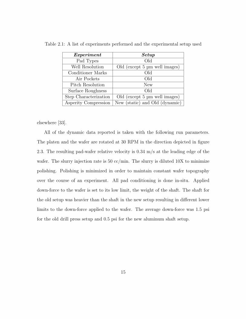
Table 2.1: A list of experiments performed and the experimental setup used
Experiment SetupPad Types Old
Well Resolution Old (except 5 µm well images)Conditioner Marks Old
Air Pockets OldPitch Resolution New
Surface Roughness OldStep Characterization Old (except 5 µm well images)Asperity Compression New (static) and Old (dynamic)
elsewhere [33].
All of the dynamic data reported is taken with the following run parameters.
The platen and the wafer are rotated at 30 RPM in the direction depicted in figure
2.3. The resulting pad-wafer relative velocity is 0.34 m/s at the leading edge of the
wafer. The slurry injection rate is 50 cc/min. The slurry is diluted 10X to minimize
polishing. Polishing is minimized in order to maintain constant wafer topography
over the course of an experiment. All pad conditioning is done in-situ. Applied
down-force to the wafer is set to its low limit, the weight of the shaft. The shaft for
the old setup was heavier than the shaft in the new setup resulting in different lower
limits to the down-force applied to the wafer. The average down-force was 1.5 psi
for the old drill press setup and 0.5 psi for the new aluminum shaft setup.
15

Figure 2.1: Most recent laboratory scale CMP tool design.
16

Figure 2.2: CMP tool used in previous research.
17

Figure 2.3: A schematic of the relative pad-wafer rotation motions and the samplingregion of interest (ROI).
18

2.1 Polishing Setup Modifications
A number of setup modifications were made during the course of this research in
order to obtain consistent measurements. A brief overview of these changes are
presented in this section. A more detailed description of the setup modifications can
be found elsewhere [45].
2.1.1 Force Table
In the original setup, down-force was applied to the wafer by using a calibrated
weighted traverse. In-situ shear forces were measured by a force transducer mounted
between a fixed plate and a plate free to slide in a single direction on linear rails.
The new setup has incorporated a force transducer table and amplifier made by
AMTI capable of measuring forces and moments applied to the polisher in all three
directions during polishing.
2.1.2 Wafer Rotation
In the original setup, the Struers RotoPol-31 polishing head was replaced by a mod-
ified drill press. The drill press is driven by a Dayton 1/2 HP motor that rotates the
wafer in the same direction as the platen as illustrated in figure 2.3. The down-force
applied by the weighted traverse from the original setup was calibrated by measuring
a static load at different traverse positions. It was assumed that the static down-
force would be the same as the dynamic down force, i.e. the down-force would be
constant in time. After the integration of the force table into the setup, it possible
19

to measure the down-force while the drill press shaft and the platen were rotating.
We found that the down-force applied to the wafer during polishing was oscillating
with an amplitude of 1.5 psi as shown in figure 2.4. In addition, the drill press shaft
was too heavy to run low down-force cases. In the new polishing setup the drill press
is replaced by an aluminum shaft driven by the same Dayton 1/2 HP motor. The
shaft is supported by aluminum beams attached to a steel vibration isolation table.
The more consistent dynamic down-force applied to the wafer in the new setup is
shown in figure 2.5.
The shaft-wafer coupling system was also modified from the old to the new setup.
In the old setup, an aluminum gimbal was epoxied to the top of the wafer such that
the center of rotation was above the wafer. A single pin through the top of the wafer
fit loosely through the drill shaft. The new wafer-shaft coupling is depicted in figure
2.6. The wafer is machined such that the end of the shaft sits at the center of the
wafer. Two pins are epoxied vertically to the top of the wafer. Perpendicular to the
pins in the wafer are the pins in the shaft that drive the rotation of the wafer.
2.1.3 Conditioning
In-situ conditioning is performed during all dynamic experiments to prevent pad
glazing, i.e. smoothing of the pad asperities that can occur during polishing. The
conditioner for the older setup was a 2 inch diameter diamond disk that rotated as
it was swept radially across the polishing pad. This diamond disk was used well
beyond the typical lifetime of a typical conditioner head. It was replaced with a 4
inch diameter diamond disk. This larger conditioner head eliminated the need to
20
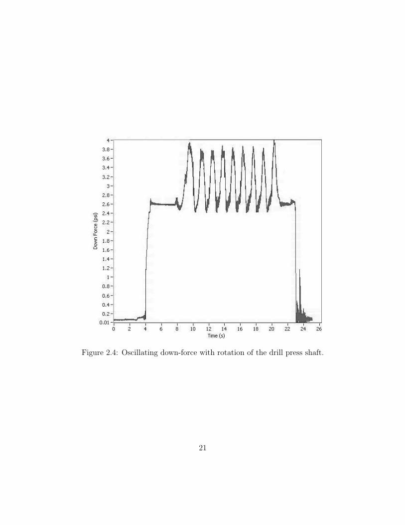
Figure 2.4: Oscillating down-force with rotation of the drill press shaft.
21
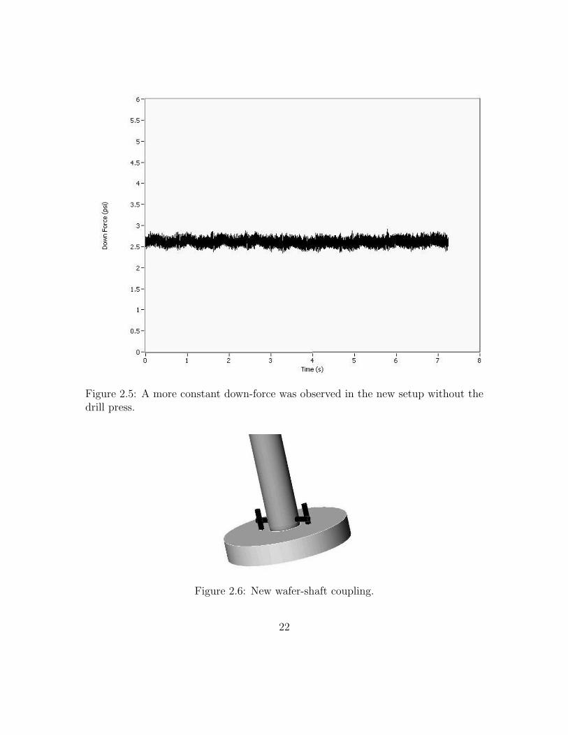
Figure 2.5: A more constant down-force was observed in the new setup without thedrill press.
Figure 2.6: New wafer-shaft coupling.
22

sweep the disk radially across the pad, and therefore just rotates over the polishing
pad directly across from the wafer. A schematic of the new conditioner system and
its motion is shown in figure 2.7.
2.2 Dual Emission Laser Induced Fluorescence
A complete discussion of how DELIF is used to measure fluid film thickness and other
passive scalar quantities has been published by research groups at Tufts University
[10], MIT [46], and University of Illinois, Urbana-Champaign [47, 48]. This section
will overview the DELIF technique, then present the specific modifications made to
the DELIF procedure for this report.
2.2.1 Theoretical Overview
Dual Emission Laser Induced Fluorescence (DELIF) is the imaging technique used
to acquire the images presented here [49]. Fluorescence occurs when an electron in
the ground state of a molecule is supplied enough energy such that it is promoted
to a higher energy state within the molecule. The electron exists in this higher
energy state for a short period of time, less than 10 ns. From the excited state, the
electron relaxes to a lower energy state either by a radiative or nonradiative decay.
A radiative decay from the excited state directly back to the ground state produces
fluorescent light. Other possible paths for the energy decay are listed in table 2.2.
In this table, the ground state is labeled ”S0”, the exited state is labeled ”S1”, and a
lower energy excited state is labeled ”T1” [50]. The ratio of the fluorescent energy to
23

Figure 2.7: Schematic of conditioning system
24

the excitation energy is the quantum efficiency, φ of the molecule. The total amount
of fluorescence, (If ) in equation 2.1, for a fluorophore in a volume is dependent upon
the the intensity of the excitation source (Ie), number of molecule (C ), the efficiency
of the absorption (ε(λ)), and the quantum efficiency [51].
If = Ieε(λ)Cφdx (2.1)
If the observed fluorescence passes through a fluid by a distance (x ), the excitation
energy is diminished a certain amount by absorption of light in that fluid. According
to Lambert’s law of absorption:
Ie(x) = I0e(−ε(λ)Cx). (2.2)
I0 is the intensity of the incident light. Therefore the thickness, δ is dependent upon
the fluorescence intensity as follows:
If (δ) =∫ δ
0I0e
(−ε(λ)C)ε(λ)Cφdx = I0φ(1− e−(ε(λ)Cδ)). (2.3)
Note that the relationship between fluorescence intensity and fluid thickness is ex-
ponential. However, the relationship becomes linear for small values of δ, or thin
films:
If ≈ I0ε(λ)Cφδ. (2.4)
When there is only one fluorophore in a system, the fluorescence observed over an
entire image is dependent on the distribution of the incident light intensity (I0). If
25

Table 2.2: Possible decay pathways for an electron in its excited state
Decay Path Name Decay Type Pathfluorescence radiative S1 → S0
internal conversion nonradiative S1 → S0
intersystem crossing nonradiative S1 → T1
phosphorescence radiative T1 → S0
intersystem crossing nonradiative T1 → S0
the light source is not uniform, then the calibration between thickness and intensity
becomes nearly impossible. To correct for source non-uniformity, one can introduce
a second fluorophore into the system that is independent of thickness, then take the
ratio of the two images effectively canceling out the excitation source as shown in
equation 2.5.
I1f
I2f
=ε1(λ)C1φ1t
ε2(λ)C2φ2
(2.5)
2.2.2 Modifications to DELIF Procedure
In the previous research [33], two dyes were dissolved in the slurry. Calcein (Fluo-
rexon), the thickness dependent dye, was mixed into the slurry at a concentration of 1
g/L, and Coumarin 4 (4 Methyl-Umbelliferone), the thickness independent dye, was
mixed into the slurry at a concentraion of 0.25 g/L. The fluorescence of polyurethane
pad was suppressed by dying the pads with carbon black.
Spectral analysis shows that the pad dying procedure only suppresses the fluo-
rescence by approximately 50%, which can lead to measurement uncertainty as high
26

as 6% [40]. Figure 2.8 shows the absorption and emission intensity as a function of
wavelength for the dyed and the undyed pads. The dashed lines indicate absorption
spectra and the solid lines are emission spectra. The absorption spectra are nor-
malized to the peak intensity value of the undyed pad absorption, and the emission
spectra are normalized to the peak emission of the undyed pad. Figure 2.8 shows
that the peak absorbance of the dyed pad is 44% of the undyed pad, and the wave-
length of the peak absorbance shifts only minimally (1nm). The peak emission of
the dyed pad is 48% of the undyed pad, and the peak shifts only 8 nm towards blue.
In this research, we take advantage of the natural pad fluorescence and use it
as the excitation source for the Calcein dye, eliminating the need for the Coumarin
4. In addition, we discovered that the Calcein is saturated in an aqueous solution
at concentrations as low as 0.5 g/L, and have therefore adjusted the amount of dye
dissolved in solution. It is possible to increase the solubility of Calcein in the slurry
by increasing the ionic strength. This can be done by adding KOH to the slurry,
but this was not done because we were able to acquire enough light from the Calcein
emission to make DELIF measurements at these lower concentrations.
A spectral analysis of the modified DELIF procedure is presented in figure 2.9.
All spectra were normalized to their peak absorbance. In figure 2.9, the y-axis is
intensity in arbitrary units (au), and the x-axis is wavelength. First a Nd/YAG laser
emits a pulse at 355 nm. That energy is absorbed by the polishing pad material and
re-emitted with an emission peak at 392 nm. There is very little spectral overlap
between the laser emission and the Calcein absorption, therefore the almost most of
the Calcein emission is due to absorption of light emitted by the pad. The Calcein
27

Figure 2.8: Fluorescence emission of dyed and undyed Fruedenberg FX9 polishingpads.
28
reemits the light with a spectral peak at 530 nm. The filter regions for each emission
are indicated in figure 2.9.
2.3 Optical Setup
Figure 2.10 shows the camera positions relative to the light paths and the region of
interest interrogated under the wafer. The emissions from the Pad and the Calcein in
the slurry pass through a beam splitter and is collected by 2 cameras. Filters in front
of each camera separate the light such that one camera records the pad emissions
and the other records the Calcein emissions. As mentioned earlier, the individual
images are affected equally by non-uniformities in the excitation source and therefore
taking the ratio of (Calcien Emission)/(Pad Emission) corrects the overall intensity
data from the 2 cameras. All images discussed in the results chapter are based upon
the ratio images.
2.3.1 Laser
Much of the work reported previously using DELIF to image CMP was done with
a UV lamp as the fluorescence excitation source. Here we us a Quantel Bril-
liant/BrilliantB Q-Switched Nd/YAG laser is used as the excitation source. The
pulse emitted has a power of 1.4W on average, a 6ns duration and a wavelength of
355 nm. The flashlamp fires at a frequency of 10 Hz, which is the maximum possible
image acquisition rate. For this work, we acquire images at a sample rate of 2 Hz to
ensure synchronization of the laser pulse and image acquisition by the cameras. Lab-
29

Figure 2.9: Spectral characterization of the pad-Calcien DELIF system.
30

Figure 2.10: Light paths and camera positions with respect to the imaging target.
VIEW software provides an interface through which the laser pulses and the cameras
can be controlled for slurry film imaging.
The laser pulse illuminates an area approximately 1 cm in diameter. This is more
than adequate for the region of interest interrogated by the cameras. However, the
polishing pads burn quickly and photodegrades when hit by the concentrated pulse.
While the photodegradation affects on the images are canceled by taking the ratio
of two images as shown in equation 2.5, the decreasing intensity in both the pad and
the slurry images will effectively decrease the accuracy of the ratio images. The laser
energy is dispersed over a wider region of the pad (1 inch in diameter) using a beam
expanding lens to maximize pad fluorescence lifetime such that we can take data sets
for longer periods of time with higher accuracy.
31

2.3.2 Pad, Wafer, Slurry
A 3 inch diameter, 0.5 inch thick, optically transparent glass wafer is used during
polishing in place of a silicon wafer and wafer carrier. The 0.5 inch thick glass wafer
is more rigid than a silicon wafer, however if we were to use a thinner wafer, slurry
would splash onto the top of the wafer obscuring parts of the image. Since the point
of the experiment is to image the polishing pad and the slurry layer, it is desirable to
limit the amount of wafer polishing. The Cab-O-Sperse SC1 slurry has been diluted
10 times such there there is minimal polishing during dynamic imaging.
Figure 2.11 depicts the paths taken by the laser light and emitted fluorescence.
The incident laser light is reflected off a mirror to the pad surface. The emission is
reflected back towards the cameras via a mirror mounted at a 450 angle to the platen.
The reflected emissions are collected by the cameras which are mounted parallel to
platen.
2.3.3 Cameras, Lens and Filters
Images are collected in two Evolution VF monochrome 12 bit linear cameras capa-
ble of 4096 gray levels. While the cameras, pictured in figure 2.12, are capable of
acquiring images 1392 pixels in width and 1040 pixels in height, it was necessary to
perform a 2x2 pixel binning to acquire enough light for the images. Therefore, the
images used for the DELIF analysis are all 696 x 520 pixels. The final ratio images
are actually smaller than 696 x 520 because the cameras are not perfectly aligned.
Due to the high magnification of the images, the alignment can be different from
day to day, which is why some of the images presented have different aspect ratios
32

Figure 2.11: Light path near the wafer.
than others. The camera gain can be set to any value between 500 and 3000. In the
older setup, the gain value was maximized to minimize noise. For the newer setup
the gain for both cameras was set to the minimum value because we are collecting
enough light such that higher values of gain would flood the cameras. However in
some cases, the gain on the Calcein camera was raised to 1000 due to low intensity
emissions. Different gain settings result in different image calibrations, therefore it
was desirable to maintain the same gain from run to run on the same experiment.
The gray box in front of the cameras in figure 2.10 contains a beam splitter and
several filters to separate the incoming light into the proper cameras. Figure 2.13
is a schematic of filter layout inside the gray box. The incident light hits a violet-
green dichroic plate beam splitter. The transmission band for this filter is 500-540nm
(green). This light then passes through an additional 490 long pass filter further filter
any additional short wavelength emissions into the camera that records the Calcein
33

Figure 2.12: Evolution VF cameras used for data acquisition.
fluorescence. The beam splitter has two reflection bands, one in the violet (395-489
nm) and one in the yellow-orange (564-655 nm). The pad fluoresces in the violet
region, therefore a 500 short pass filter is place in front of the second camera to filter
the yellow-orange reflection.
Not shown in figure 2.10 (but probably should be in the final version of my thesis)
is a Nikon 135mm f/5.6 EL-Nikkor Enlarging Lens, shown in figure 2.14. The lens
is from the CCD elements in the cameras by 18 inches. The resulting field of view
for each camera is 3.0 mm x 2.3 mm. The f stop on the lens is fully open such that
the maximum amount of light can be acquired.
34

Figure 2.13: Filters and beam-splitter locations.
Figure 2.14: Nikon 135mm f/5.6 El-Nikkor enlarging lens
35

Chapter 3
Image Calibration
Calibration of pixel intensity to the height of a column of fluid is extraordinarily
important for acquiring accurate quantitative results. Unfortunately, calibration for
the modified DELIF procedure described in section 2.2.2 is not straight forward.
Three calibrations techniques are mentioned in this chapter. The calibration tech-
nique that is used for quantitative analysis is described in section 3.2.2. In section
3.3 I describe the problems associated with the calibration technique.
Images are acquired using 4 different wafers, a flat wafer, a wafer with 27 µm
deep wells, a wafer with 14.5 µm deep wells, and a wafer with 5 µm deep wells. A
schematic of the wafers with wells can be seen in figure 3.1. The wafers with 27 and
14.5 µm deep wells serve as both a tool for studying pad deformation (chapter 4)
and a method for calculating the correlation factor between slurry layer thickness
and intensity (section 3.3.2).
36

3.1 Wafer Etching
The 3” diameter, 0.5” thick BK7 optical glass blanks were sent to Intel where the
following etch procedure was performed:
1. Clean glass surface (detergent, DI water rinse, Marangoni dry, 5 minutes oxygen
plasma)
2. Sputter 150.0 nm Au on 5.0 nm Cr
3. Dip coat photoresist
4. Cure photoresist at 80 degrees C for 10 minutes
5. Photopattern resist (expose for 45 s, develop for 120 s)
6. Hand paint wafer edges (not covered by pattern mask), develop, dry and bake
at 80 degrees C for 10 minutes.
7. Wet etch Au and Cr in well regions for 30 s
8. Etch glass in well regions using 40 mL 48 % HF in 360 mL DI water
9. Strip photoresist with acetone and isopropanol
10. Etch the remainder of the Au and Cr
The HF etch time for the 27 µm well was 33 minutes and the etch time for
the 14.5 µm well was 17 minutes. This etching procedure was complicated by the
fact that the wafers had already been mounted onto a gimbal making it hard to
37
deposit the Au/Cr mask and the photoresist. As a result, the wafers displayed
large irregular undercuts with a high density of pinholes. While these undercuts and
pinholes would be unacceptable for state of the art ICs, they are undetectable at the
imaging resolution discussed in this experiment. Step heights were verified using a
profilometer. All well depths were the same height with ±0.01 µm.
The patterning mask covers a square region 2”x2” on the wafer. Figure 3.1 shows
resulting pattern on the wafer after the etch procedure. There are 17 rows of wells.
The top row contains 0.5mm x 0.5mm square wells separated by a distance of 1mm.
The second row contains equally spaced squares slightly smaller than 1mm on each
side such that 1 cm contains the equivalent of 6 squares and 5 spaces. The third
row contains 1mm x 1mm square wells separated by 1mm. The fourth row contains
1.5mm x 1.5mm squares separated by 1.5mm spaces. The fifth row contains 2mm
x 2mm squares separated by 2mm spaces. Each row is separated by 2mm and the
set of five rows repeats across the area. The different well areas and spaces between
them are used to test how fast pad asperities rebound into the wells.
3.2 Calibration
The x and y directions on the images were calibrated by the photographing a mil-
limeter ruler as shown in figure 3.2. The number of pixels between the start of one
hash mark and the next were counted. The resulting image resolution at the present
zoom factor is 4.3 µm per pixel.
Correlation of the intensity values, I, to fluid film thickness, T, recorded in the z
38
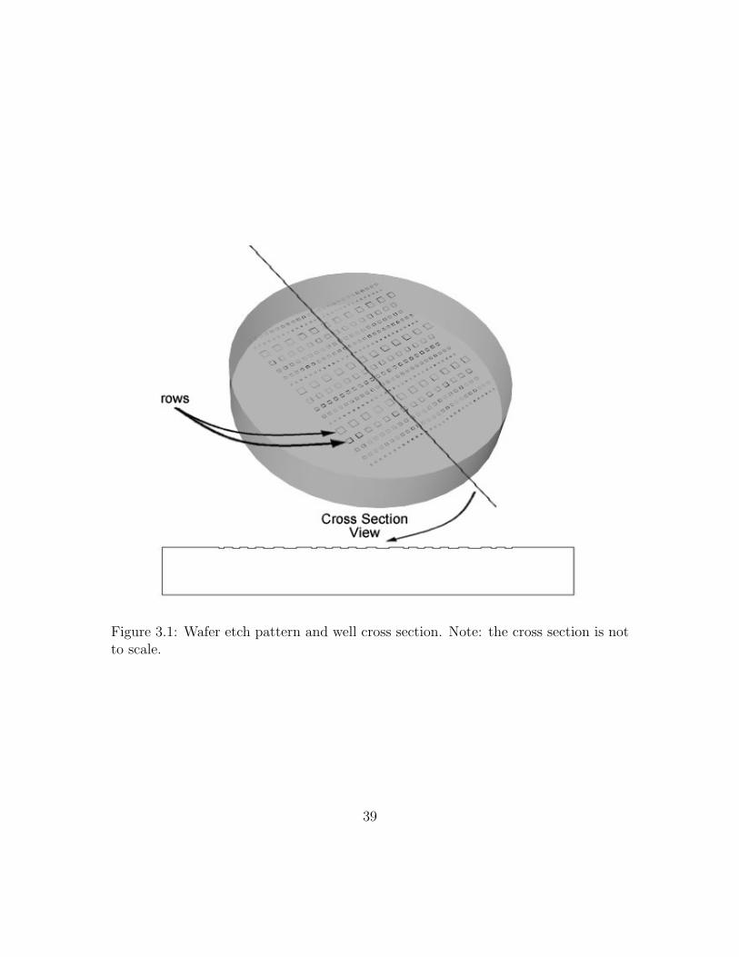
Figure 3.1: Wafer etch pattern and well cross section. Note: the cross section is notto scale.
39

Figure 3.2: Image used for x-y pixel calibration
direction is not a trivial task and is therefore the subject of the following subsections.
Previous work has proven that the relationship between fluid film thickness and ratio
is close to linear [16]. Therefore we should be able to express thickness as a function
of intensity, δ(I), as shown in the following equation:
δ(I) = XI + δ(0), (3.1)
where X is the calibration factor.
3.2.1 Previous Calibration Attempts
A schematic of other possible calibration procedures is shown in figure 3.3. Figure
3.3a is the method that has been used in previous research [33] in which the slurry fills
40

the gap between the microscopes calibration slides. This method became difficult
to use when we changed the DELIF procedure to use the pad fluorescence as the
excitation source. It became hard to determine how much light from the pad was
able to make it through the microscope slide to excite the Calcein in the slurry.
We determined that the slurry should be in direct contact with the pad for the
calibration. Figure 3.3b shows another calibration procedure we had considered.
One edge of a flat BK7 glass wafer was propped up 1mm from the polishing pad
surface such that there was a known sloping volume of slurry under the wafer. This
technique was not used for a number of reasons. First, it was difficult to determine the
exact slope of the wafer because it was difficult to repeatedly place the microscope
slide in the same place. Second, a single cross section showed a large amount of
asperity noise. Finally, it was difficult to image the edge of the wafer or find the
exact position of the image on the wafer with the decreased field of view in these
experiments. The calibration technique that was finally used is shown in figure 3.4
and is discussed in section 3.2.2.
3.2.2 Relative Thickness
Most of the analysis presented, such as surface roughness, asperity compression, a
fluid layer step heights, are determined by directly comparing one region of the image
to another region or the mean. Therefore, the offset value, δ(0) in equation 3.1, is
canceled in a subtraction. The calibration equation simplifies to
∆δ(I) = X∆I. (3.2)
41

Figure 3.3: Previously used calibration techniques (a) Microscope slides with a shim,(b) Flat wafer over the pad at an angle produced by microscope slide.
The two wafers with the square wells of known depth can be used to determine
X. This calibration is based on the assumption that both the 14.5 µm and 27 µm
deep wells are deep enough such that the tops of the asperities, on average, are not
in contact with the bottoms of the wells, and there is no significant angle between
the wafer and the pad in the region of interest. Since the polishing pad rebounds a
certain unknown distance into each wells, it is not possible to simply say that the
average intensity under a well is equal to the height of the well. However, it may be
possible to assume that the difference in intensities between the 14.5 µm and the 27
µm deep wells is roughly equal to the difference in step heights, 12.5 µm. This leads
to the following equation for calculating X :
X =27− 14.5
I27 − I14.5
. (3.3)
For most runs, the calibration factor attained was 70 µm per ratio unit. A schematic
42

of this calibration procedure can be seen in figure 3.4. This assumes that the wafer
is flat and that the asperity rebound into the wells is independent of well depth.
3.2.3 Absolute Thickness
An absolute calibration would allow the direct assignment of an accurate slurry layer
thickness value at every pixel in an image. If the intensity in the Calcein camera
is zero when no Calcein is present, then the thickness value at zero intensity would
be zero, δ(0) = 0. Additionally, the relative calibration discussed above would be a
valid absolute calibration. However, the intensity values of a ratiod image with no
Calcein are not zero even with dark noise values subtracted from the image because
the image filters can not filter out 100% of the pad fluorescence. The dark-noise
is the average intensity over an image taken with no ambient room lighting and no
laser shot. Since ratio values actually drift from run to run and image to image, it is
extraordinarily difficult to determine δ(0). The lowest ratio intensity values observed
range from 0.3 to 0.5. Techniques for determining the zero point intensity is still a
limitation of the system and are discussed elsewhere [45].
Figure 3.4: Schematic of the method used to determine the relative thickness cali-bration factor.
43

3.3 Experimental Sources of Error
There are two major sources of error in these experiments. First, the average in-
tensity of an image increases with the number of laser shots to that location on the
polishing pad. As a result, the image to image calibration factor, X, increases in time
according to equation 3.2. Possible reasons for this are examined by evaluating the
individual fluorescing components in the DELIF system as observed through each
camera. The second source of error is the uncertainty in determining the ratio value
that corresponds to zero thickness. This is only briefly discussed here because it is
discussed in greater detail elsewhere [45].
3.3.1 DELIF
One of the largest sources of error in this set of experiments is ratio drift in time. The
average image intensity over a run even as short as 20 image shows a positive slope.
The polyurethane pad is known to photodegrade with exposure time to UV light.
However, if the pad fluorescence intensity decreases and the Calcein fluorescence is
dependent on the intensity of the pad, the Calcein fluorescence should also decrease
with pad fluorescence. The ratio should therefore be constant. Unfortunately, the
ratio does increase with time. To investigate ratio drift, each DELIF component
was examined separately. The results are shown in figures 3.5, 3.6, and 3.7. When
examining these figures, it is important to keep in mind that the dark noise values
for both cameras has an intensity of roughly 180. Below is a list of the 5 components
presented in the graphs:
44

1. diamonds = the ”control pad”, which is a sheet of black rubber that we assume
does not fluoresce
2. squares = Calcein in the slurry on top of the control pad
3. triangles = the Fruedenberg FX9 pad
4. circles = the ”run conditions”, which is Calcein in the slurry on top of a
Fruedenberg FX9 pad
5. stars = slurry without Calcein on a Fruedenberg FX9 pad
Figures 3.5 and 3.6 show the intensity data from the above samples as seen
through the Calcein camera and pad camera, respectively. The control pad (dia-
monds) shows intensities that are roughly the same value for both cameras with zero
slope in time. Note that the control pad intensity is above the dark-noise. This is
because the black rubber is not a ”perfect” optical black, meaning that some of the
laser light is reflected back into the cameras. The filters do not filter out 100% of
the laser light, otherwise the control pad line would lie on top of the dark-noise line.
Figure 3.5 examines the intensity as seen through the Calcein camera. Just
above the control pad line are the pad (triangles) and undyed slurry (stars) lines,
which lie roughly on top of each other with a very small positive slope. The fact
that these two lines are not directly on top of the control pad line indicates that
the filters for the Calcein camera don’t completely filter out all of the light from
the pad fluorescence. However, the amount of pad fluorescence is small and roughly
constant and should therefore be accounted for in the calibration factor (provided we
45

can attain an accurate calibration factor). The slope of these lines over this sample
space is negligible. However, the fact that it is positive is problematic since there is
no Calcein present in either of these cases and the pad is know to photodegrade in
time. In the future it may be worth the time investment to observe the pad as seen
through the Calcein camera over a larger number of images to determine if this is a
true slope or experimental noise.
The Calcein line (squares) in figure 3.5 has an average intensity 2.5 times the dark
noise and 2 times greater than the control pad. This means that the Calcein receives
a small excitation from the laser assuming that the control pad does not fluoresce.
Figure 2.9 also shows that the absorbance of Calcein in the region of the laser is not
zero, but it is near a minimum. There is also a positive slope to this line, which also
supports the idea that the Calcein may be an excitation source for itself. Note that
there is a spectral overlap between the Calcein absorbance and emission in figure 2.9
making it possible for the Calcein emission to produce subsequent self-reabsorption.
The average intensity of the Calcein under full run conditions (circles) is only about
three times greater than the Calcein by itself. As shown in figure 2.9, the spectral
overlap between the Calcein absorbance and the pad fluorescence is not very large.
However it is large enough to induce sufficiently detectable Calcein fluorescence with
the current filter setup. In addition to the run condition intensity being 3 times
greater than the Calcein alone, it also seems that the slope of the run conditions
line is about 3 times greater than the Calcein line. This suggests that when the pad
induced Calcein fluorescence is greater, there is more reabsorption of the Calcein
fluorescence by the Calcein.
46

Figure 3.5: DELIF components as seen through the Calcein camera.
47

Figure 3.6 shows intensities of the components as seen through the pad camera,
the denominator of the ratio DELIF images. The control pad (diamonds) and the
Calcein (squares) lines have no slope in time and have a value of a little less than
twice the dark noise. This means that the pad camera is effectively filtering out
all the Calcein fluorescence, but some of the laser light is seeping through the filter
making the total intensity greater than the dark noise. The pad (triangles) and the
undyed slurry on the pad (stars) lines in figure 3.6 have the highest intensities and
both have negative slopes. The negative slopes mean that the pad is photodegrading
in time. It is unclear why the intensity of the pad with undyed slurry over it has a
higher intensity than the pad without slurry. Perhaps different sections of the pad
fluoresce less intensely, or the laser power may have shifted slightly between tests, or
perhaps the slurry particles are reflecting some of the incident light back towards the
cameras. The run condition (circles) intensity is lower the pad and undyed slurry
lines because some of the pad fluorescence is being absorbed by the Calcein. Unlike
the pad and the undyed slurry lines, the run conditions line initially has a negative
slope showing the photodegration of the pad, but the line levels by about image 10.
From examination of these data, one might conclude that the Calcein is reaching
a saturation point in the amount of pad fluorescence it can absorb and perhaps a
higher concentration of Calcein is needed. Increasing the concentration of Calcein is
difficult because of its limited solubility in water.
When the Calcein camera images are divided by the pad camera images, the
result is figure 3.7. Here, the FX9 pad (triangles) and the undyed slurry (stars)
show the smallest ratio values and are very nearly consistent with each other. This
48
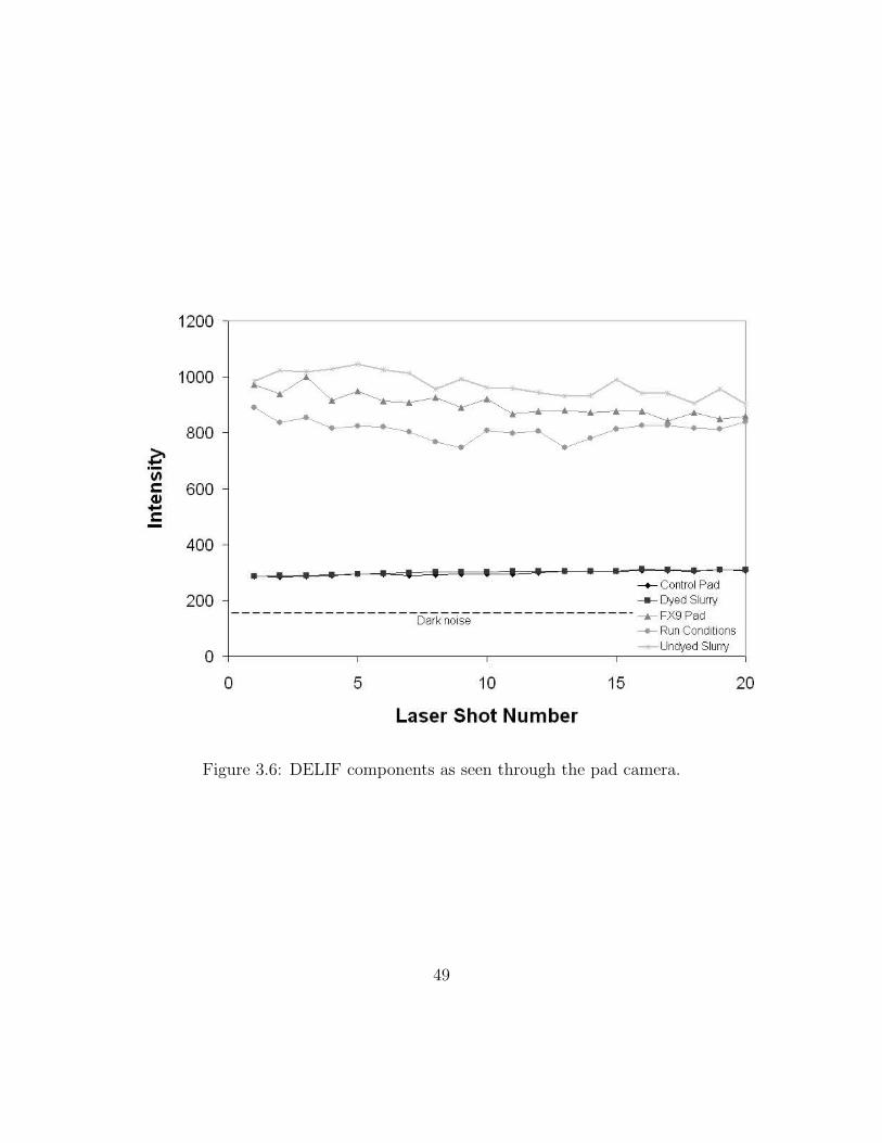
Figure 3.6: DELIF components as seen through the pad camera.
49

is because there is no Calcein present in these systems and there is a large amount
of pad fluorescence. There is a slightly positive slope due to the photodegradation
of the pad. The dyed slurry (squares) has the highest intensity because there is no
pad fluorescence. The Calcein is minimally excited by the laser, then it is excited by
itself creating a positively sloping line. The control pad (diamonds) has a constant
ratio in time of approximately 0.6, which is the ratio of the laser light reflected off the
black rubber pad that is not filtered by the cameras. From the control pad line on
this graph, we can conclude the Calcein camera filters are 40 percent more efficient
in filtering the laser light than the pad camera filters. Finally, the line with circles
indicates the observed ratio drift under full run conditions. It has the most positive
slope on this graph because Calcein fluorescence in the numerator has a consistently
positive slope, and the pad fluorescence in the denominator has a negative slope until
image 10 and then levels off.
The effect of Calcein self excitation would be minimized if the spectral overlap
between the pad emission and the Calcein absorption was significantly greater than
the spectral overlap between the Calcein emission and the Calcein absorption. That
overlap can be calculated from figure 2.9 by summing the areas under the overlap
regions of the curves. The pad emission/Calcein absorption overlap is only 2.3 times
greater than the Calcein emission/Calcein Absorption overlap.
3.3.2 Calibration
The next chapter contains both a qualitative and quantitative analysis of the im-
ages. The calibration factor of 70 µm/ratio unit is used for most of the quantitative
50

Figure 3.7: Final ratio of the Calcein camera images divided by the pad cameraimages.
51

analysis. However this calibration factor is only accurate to about ±10 µm because
of the ratio drift discussed in section 3.3.1. This error was calculated using the
method discussed in section 3.2.2 and equation 3.3, using the 27 µm and 14.5 µm
deep wafers. A run of 50 images was taken first with the 14.5 µm deep wafer, then
a run of 50 images of the 27 µm deep wafer, followed by a third run which was a
re-run of the 14.5 µm deep wafer. The calibration factor calculated using the first
and the second run was approximately 60 µm/ratio unit, and the calibration factor
for the second and third run was approximately 80 µm/ratio unit. Calibrations have
been performed for every dynamic experiment involving wafers with square wells. All
values for the calibration factor have been roughly within error of 70±10 µm/ratio
unit. This error may seem large, but keep in mind that the average peak to valley
height for an asperity on a Fruedenberg FX9 polishing pad is approximately 10 µm,
which corresponds to an approximate intensity difference of 0.14 ratio units. The
calibrated height of 0.14 ratio units would be 10±1.4 µm (a 14% error).
The reader should also keep in mind that some graphs presented in chapter 4 (for
example figure 4.27) will show absolute thickness values. These values for absolute
thickness were calibrated using the relative calibration factor discussed in section
3.2.2 and it is still unclear what value of the ratio actually corresponds to zero thick-
ness, the image was calibrated with the relative calibration factor. The difference
between y values will be accurate, however the actual y-values may vary by as much
as 20 µm.
52

Chapter 4
Image Analysis
Thousands of images were taken over the course of this research. A physical inter-
pretation of the images is presented in this chapter. The images are analyzed both
qualitatively and quantitatively. In the qualitative section, the resolution of wafer
and pad features is discussed, and air entrapment between the wafer and the pad is
examined. In the quantitative section, the images are calibrated using the factor dis-
cussed in section 3.3.2. Only the Fruedenberg FX9 pad (see section 4.1.1) was used
to make quantitative measurements for result consistency. First, pad topography is
discussed. Then the slurry layer profile is used to interpret pad compliance to the
wafer features shown in figure 3.1. Three analysis techniques are discussed: calcu-
lating surface roughness, fitting averages of cross section to a step-like function, and
comparing histograms of images to determine the amount of compression at different
pressures.
Some of the images discussed in the following sections are static, and others
53

are dynamic. For the static images, tagged slurry was deposited onto the polishing
pad and the wafer was gently placed on top of the slurry with the force of the
shaft pressing down on it. There was no pad-wafer rotation or conditioning during
the image acquisition. The pad for the static images were conditioned before image
acquisition. The dynamic images were taken with the pad and the wafer both rotating
at 30 RPM, which means the pad-wafer relative velocity at the leading edge of the
wafer was 0.34 m/s. Slurry was injected at the middle of the pad at 50 cc/min. The
pad was conditioned for 20-30 minutes before image acquisition with undyed slurry
and conditioned continuously during acquisition with dyed slurry. Between 50 and
200 images were taken during each dynamic run.
4.1 Qualitative Image Analysis
All images presented in this section are processed images of the ratio obtained by
dividing the Calcein fluorescence intensity by the pad fluorescence intensity. Images
were taken while the platen and the wafer were both in rotation, and those presented
here were picked from thousands of available images. The dark areas in the image
correspond to low values of the ratio of intensities and indicate where the pad and
the wafer are close to each other, or the tops of the pad asperities. Conversely, the
lighter sections of the image indicate high values of the ratio and slurry filled valleys
between pad asperities. The images presented in this section were chosen out of the
thousands taken because they are representative of the various types of pads, wafers
and slurry characteristics observed during the various runs.
54

4.1.1 Images of Different Types of Pads
In this section, DELIF Images of several types of polishing pads will be discussed.
Multiple types of pads were tested such that we could test the resolution of the
DELIF imaging at the new zoom factor. The pads types used are listed below:
• Flat Fruedenberg FX9 (dyed), figure 4.2a
• Flat Fruedenberg FX9 (undyed), figure 4.2b
• k-grooved Fruedenberg FX9, figure 4.3a
• k-grooved Rodel IC1000, figure 4.3b
• Thin-grooved Experimental CMC M2, figure 4.4a
• Flat Experimental CMC M2, figure 4.4b
• xy-grooved Experimental CMC M3, figure 4.4c
The grooving is defined in figure 4.1. The xy-grooves and thin-grooves differ only in
trench depth. The k-grooved pads are grooved in concentric circles and have trenches
shaped like the letter ”k”.
For most pads, images were taken with three different wafer surfaces: a flat wafer,
the wafer with 14.5 µm deep wells, and the wafer with 27 µm deep wells. Figure
4.2a is an image of a dyed flat Fruedenberg FX9 pad, figure 4.2b is an undyed
Fruedenberg FX9 pad. The Fruedenberg FX9 pads are very similar to the industrial
standard Rodel IC1000 pads. The undyed FX9 pad is not smoother than the dyed
pad even though it might appear that way. The focus on the cameras during the
55

Figure 4.1: Pad Grooving (not to scale). The left is an image of an xy-grooved andthin-grooved pad. The right is an image of a k-grooved pad.
run with the undyed FX9 pads was not as sharp as the focus during the dyed pad
run. We did not rerun these images because most of the quantitative measurements
were done on the dyed FX9 pads. The point of taking images on the undyed pads
was to prove that it could be done. The surface roughness measurements (discussed
in section 4.2.2) show the same results for the focused and less focused images.
Figure 4.3 presents the two k-grooved pads. Image ”a” is the Fruedenberg pad and
image ”b” is the Rodel pad. The groove width is 4 times wider on the Fruedenberg
pad than the Rodel pad. In both cases, the grooves contain so much fluid that the
intensity inside the grooves is flooded. There are bands of lower intensities on each
side of the grooves. These bands are not believed to be real thickness, but artifacts
of light bleeding into pixels adjacent to the high intensity grooved regions.
56

Figure 4.2: DELIF images of flat Fruedneberg FX9 polishing pads (a) Dyed (b)undyed
57

Figure 4.3: DELIF images of pads with k-grooves (a) Fruedenberg FX9 (b) RodelIC1000
58

Figure 4.4 includes images from experimental polishing pads produced by Cabot
Microelectronics Corporation (CMC). Figure 4.4a show the slurry layer between a
flat BK7 wafer and the M2 thin grooved pad. Figure 4.4b shows fluid over an M2
thin-grooved pad and Figure 4.4c shows images on an M3 xy-grooved pad. The M3
pad is slightly smoother than the M2 pad. Besides the obvious groove, the dominant
features in Fig. 4.4 are cross-hatched regions of high intensity indicating a pattern
of valleys in the pad. This pattern was imprinted onto the pad and tests the ability
of the DELIF technique to observe larger scale features. The cross-hatches will not
be present in the final version of this experimental pad.
4.1.2 Well Resolution
Figure 4.5 shows wafers with etched wells over a flat Fruedenberg FX9 polishing
pad. Figure 4.5a shows a DELIF image of the wafer containing 14.5 µm deep wells,
and figure 4.5b is an image of the wafer containing 27 µm deep wells. Figure 4.6
shows 5 µm deep wells over an undyed FX9 pad with a sub-pad. Figre 4.6a is the
original image taken and the wells are present, but hard to resolve. Figure 4.6b is an
enhanced image in which the contrast and levels were adjusted to resolve the wells.
The enhancement was done by adjusting the gray-scale look-up table levels until the
square could be adequately resolved. All quantitative analysis is done on the original
images. The darker areas in the image indicate a thinner slurry layer and, hence,
a smaller distance between the polishing pad and the wafer. Conversely, brighter
section of the image indicates a thicker slurry layer and a larger distance between
the pad and the wafer. Note that in addition to the ability to resolve well regions,
59

Figure 4.4: DELIF images of CMC experimental pads (a) Flat CMC M2 (b) thin-grooved CMC M2 (c) xy-grooved CMC M3
the images also contain good definition of the pad asperities both inside and outside
the wells. The 5 µm deep wells are near the limit of this technique’s ability to resolve
wafer feature over this pad. All of the quantitative analysis is done on these flat
Fruedenberg FX9 pads because of the high DELIF resolution capabilities.
Figures 4.7 and 4.8 show the wells over a k-grooved Rodel IC1000 pad and a
k-grooved Fruedenberg FX9 pad, respectively. It is more difficult to resolve the
well in these images without image enhancement because the amount of slurry in
the groove is significantly greater than outside the groove. The resulting intensity
contrast between regions inside the well and outside the well is greatly diminished.
Therefore resolving any pad features on the asperity level is nearly impossible for this
optical setup. In order to resolve the asperities, we would have to increase the gain
60

Figure 4.5: DELIF image of wafers with etched square wells over the flat, dyedFruedenberg FX9 pad (a) 1 mm2, 14.5 µm deep well (b) 1 mm2, 27 µm deep well
Figure 4.6: DELIF image of a wafer with 5 µm deep wells on an undyed, flat Frue-denberg FX9 with sub-pad. (a) original image (b) enhanced image
61

and/or the exposure time such the contrast between the asperity hills and valleys. At
the new camera settings, the camera pixels in the grooved regions would flood and
the light would bleed into nearby pixels. Therefore, we did not attempt to resolve
the asperities in these images. Enhanced images where the wells are resolved can be
seen in figure 4.9. The enhancement was performed in a similar manner as in figure
4.6b.
Wells over the experimental CMC pads are not shown because these images look
exactly the same as the images of a flat wafer over these pads. The surface roughness
of these pads is an order of magnitude larger than the Fruedenberg FX9 and Rodel
IC1000 pads. Wells could not even be resolved on CMC experimental M2 pads
without grooves. Therefore, the intensity contrast between asperities in the Cabot
pads overshadows even a 27 µm deep well. These large asperities limit our ability to
make any quantitative measurements.
4.1.3 Conditioner Marks on Pads
Most images from the flat Fruedenberg FX9 pads show patterns in the asperities as
indicated by the dashed lines in Figure 4.10. The striation lines in figure 4.10a run
from the top left to bottom right at almost 45 degrees. In figure 4.10b the striation
lines are just off the horizontal with a slightly positive slope. These lines are most
likely gouges in the pad caused by the diamond grit conditioner. Figure 4.10b shows
a slurry layer beneath a 14.5 µm deep, 1000 µm square well etched into the BK7
wafer over a Freudenberg FX9 polishing pad.
62

Figure 4.7: Well resolution over the Rodel IC1000 k-grooved pad (a) 14.5 µm deepwells (b) 27 µm deep wells
63

Figure 4.8: Well resolution over the Fruedenberg FX9 k-grooved pad (a) 14.5 µmdeep wells (b) 27 µm deep wells
Figure 4.9: Enhanced images of figures 4.7 and 4.8.
64

Figure 4.10: Pad striations caused by the conditioner on a flat Fruedenberg FX9polishing pad under (a) a flat wafer (b) 14.5 µm deep wells
65

4.1.4 Air Pockets
Another interesting feature we observed was the formation of air pockets underneath
the 27 µm deep wells. The presence of air pockets during polishing is not typically
considered in fluid flow modeling between the pad and the wafer. Air pockets could
have a significant effect on removal rate near wafer features and post polishing wafer
topography. Figure 4.11 contains images of these air pockets under the 27 µm deep
on a Freudenberg FX9 pad. The arrows in the figure show the direction of slurry
flow. Air pockets were not observed under the 14.5 µm wells and were present in
approximately 50% of the images of the 27 µm deep wells. The majority of the
images of the full square wells showed air bubbles of different sizes moving across
the wells. Figure 4.11a shows an air pocket in the center of a well. The irregular
shape can probably be attributed to slurry flowing around different size asperities.
The majority of the air pockets from the runs with a 27 µm deep wells are similar
to Fig. 4.11b, showing air pockets in the upper left corner of the wells, which is the
trailing edge of the slurry flow. Figure 4.11c shows one of the larger air pockets as
it is dissipating through the contact region just behind the trailing edge of the well.
One can also see the slurry in the pad below the air pocket, implying that one can
estimate the dimensions and volume of the air bubble by comparing the fluorescence
under the well outside of the air bubble as compared to inside the air bubble.
The presence of air pockets is not limited to flat pads. Air can also be seen both
under the wells and in the grooves of grooved pads. Figure 4.12 shows images of
a BK7 wafer with 27 µm wells over a Rodel IC1000 k-grooved pad (a) and over a
Fruedenberg FX9 k-grooved pad. While the grooved in the Fruedenberg pad are
66

Figure 4.11: Air pockets under 27 µm deep wells on a Fruedenberg FX9 pad (a)Middle of well (b) Trailing edge of well (c) Air dissipating from inside to outside thewell
67
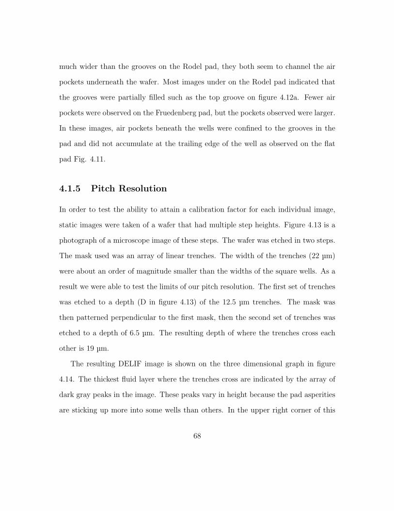
much wider than the grooves on the Rodel pad, they both seem to channel the air
pockets underneath the wafer. Most images under on the Rodel pad indicated that
the grooves were partially filled such as the top groove on figure 4.12a. Fewer air
pockets were observed on the Fruedenberg pad, but the pockets observed were larger.
In these images, air pockets beneath the wells were confined to the grooves in the
pad and did not accumulate at the trailing edge of the well as observed on the flat
pad Fig. 4.11.
4.1.5 Pitch Resolution
In order to test the ability to attain a calibration factor for each individual image,
static images were taken of a wafer that had multiple step heights. Figure 4.13 is a
photograph of a microscope image of these steps. The wafer was etched in two steps.
The mask used was an array of linear trenches. The width of the trenches (22 µm)
were about an order of magnitude smaller than the widths of the square wells. As a
result we were able to test the limits of our pitch resolution. The first set of trenches
was etched to a depth (D in figure 4.13) of the 12.5 µm trenches. The mask was
then patterned perpendicular to the first mask, then the second set of trenches was
etched to a depth of 6.5 µm. The resulting depth of where the trenches cross each
other is 19 µm.
The resulting DELIF image is shown on the three dimensional graph in figure
4.14. The thickest fluid layer where the trenches cross are indicated by the array of
dark gray peaks in the image. These peaks vary in height because the pad asperities
are sticking up more into some wells than others. In the upper right corner of this
68

Figure 4.12: The air pockets are confined to the grooves under the 27 µm deep wells(a) Rodel IC1000 k-grooved pad (b) Fruedenberg FX9 k-grooved pad
69

Figure 4.13: Microscope image of a wafer etched trenches of different depths
70
image there is a region of lower intensity where one would expect to see dark gray
peaks. It is in this region where the asperities are reaching the farthest into the wells.
There is more connectivity in the peaks in the horizontal direction than the vertical
direction. This means that the 12.5 µm deep trenches run horizontally across the
images, while the smaller 6.5 µm trenches run vertically across the images.
While the trench overlap regions are relatively easy to identify, the individual
trenches are harder to see due to the shape of the polishing pad. In an attempt to
resolve the trenches, 100 cross section in both the horizontal and vertical directions
were averaged together. The resulting average cross sections can be seen in figures
4.15 and 4.16. The average peak to valley height in figure 4.15 is 0.124±0.044 ratio
units, whereas the average peak to valley height in figure 4.16 is 0.061±0.19 ratio
units. In addition to resolving the trenches, this cross section averaging has revealed
that there is a fair amount of pad waviness across this image. There is a high point
in the pad near where the ratio is smallest: around 650 µm in figure 4.15 and around
1050 µm in figure 4.16. The corresponds to the highest concentration of green in the
top right of figure 4.14.
Wafers with multiple well depths can potentially be used for in-situ calibration.
Once the average peak to valley ratio in both directions has been determined, it can
be compared to the known average height for those cross sections. Keep in mind
that there were actually 2 types of cross sections that were averaged together for
each graph in figures 4.15 and 4.16. A cartoon of these possible cross sections can
be seen in figure 4.17. According to the dimensions in figure 4.13, 36% of the cross
sections should be inside a trench and 64% of the cross sections are not inside a
71

Figure 4.14: 3D DELIF image of a wafer with multiple step heights over a flatFruedenberg FX9 polishing pad
72
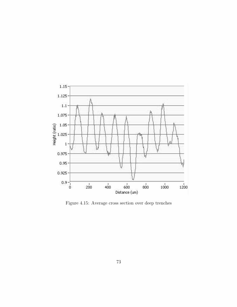
Figure 4.15: Average cross section over deep trenches
73

Figure 4.16: Average Cross section over shallow trenches
74

trench. Therefore, the actual average peak to valley height for figure 4.17 should be:
[(0.64× 6.5) + (0.36× 19)]− [(0.64× 0) + (0.36× 6.5)] = 8.66µm (4.1)
For the cross sections over the 12.5 µm deep trenches, the average peak to valley
height should be 10.34 µm. This image can now be calibrated using an equation
similar to equation 3.3. The resulting calibration factor is X = 26 µm/ratio unit.
This number has a high degree of inaccuracy due to the large error in calculating
the peak to valley height from the pad waviness. There is more than 30% error in
the individual peak-valley measurements, therefore, when the error is propagated
through the calibration calculation, the resulting error is more than 65%.
4.2 Quantitative Image Analysis
Three methods of quantitative image analysis are presented in this section. Pad
surface roughness is calculated inside and outside the wells for dynamic runs on all
three patterned depths (5-27 µm). The average step cross section is calculated and fit
to a curve that reveals how quickly the polish pad conforms to the step in the wafer.
Finally, asperity compression is calculated by comparing histograms of the intensities
within the data sets. All data in this section were collected on a the Fruedenberg
FX9 polishing pad because they were readily available and we were able to achieve
the highest image resolution on these pads (see sections 4.1.1 and 4.1.2). Before the
analysis methods are discussed, I give an overview the Fruedenberg FX9 polishing
75

Figure 4.17: Schematic of trench averaging
pad topography because pad waviness plays a significant role in the results of the
image analysis.
4.2.1 Fruedenberg FX9 Pad Characterization
Pad waviness should be considered before discussing surface roughness, pad shape
near wafer features and asperity compression because the average fluid layer thickness
and pad-wafer slope changes with pad rotation. Figure 4.18 shows a profilometer
scan across the 76.2 mm region of the pad; this sample length was chosen because
it is the same as the wafer diameter (3”). Note that in addition to pad asperities
(micron-scale topography) there is also a fair amount of global pad topography or
pad waviness. The imaged measurement areas are approximately 6 mm2 regions,
which will only show the micron-scale topography. The wafer will be resting only on
the highest portion of the pad, therefore, the average slurry film thickness in each
image varies depending on the pad’s global topography. In addition, the image-to-
image slurry film thickness during a run and applied global down-force to the wafer
76

correlate poorly due to the relatively small size of the imaging region.
4.2.2 Surface Roughness
The surface roughness results reported here refer to the shape of the slurry layer and
not the shape of the pad. If there are no air pockets between the flat surface of a
wafer and the polishing pad, then the slurry fluid is assumed to conform to the shape
of the pad surface filling the valleys between asperities. The roughness of the slurry
layer with no air pockets is then the roughness of the pad under flat sections of the
wafer. For each image, a region of interest is chosen in a region that is not near a
well edge with length, m, and width, n. The most commonly used measurement is
the arithmetic mean roughness, Ra, which is arithmetic average of the deviations of
heights from the mean. Ra is calculated as follows:
Ra =(
X
m · n
) m∑i=0
n∑j=0
|Ii,j − I| (4.2)
where I is the mean intensity in the region and Ii,j is the intensity at pixel location
(i,j).
Figure 4.19 is a cartoon of what we believe is happening to the pad as it passes
by a wafer feature in figure 4.10b. Depending on where you are on the pad, the
value for the mean slurry layer thickness inside and outside the wells will vary. In
this cartoon, the mean thickness outside the well is 14.6 µm, and the mean thick-
ness inside the well is 26 µm. The slurry layer roughness, and therefore the pad
surface roughnesses measured inside and outside the well are 4.6 µm and 3.8 µm,
77

Figure 4.18: Profilometer scan of a Fruedenberg FX9 polishing pad. The imagedregion is magnified in the inlay.
respectively. The mean asperity height is twice the surface roughness, therefore the
mean difference in asperity height from inside to outside the well is 2x(4.6-3.8) =
1.6 µm. Profilometer measurements of the Freudenberg FX9 pad indicate a surface
roughness, Ra = 4.3 +/- 0.3 µm, suggesting that the asperity peak-to-valley height
averages around 8.6 µm. This profilometer measurement is within error of the actual
surface roughness estimation from the DELIF image, meaning that the asperities are
compressed outside the well region, then are expanding to their full height under the
wells.
Analysis of surface roughness over successive images from the run that produced
figure 4.10b show that the average roughness beneath the contact regions outside
the well is consistently less than the roughness beneath the wells. These data sug-
78
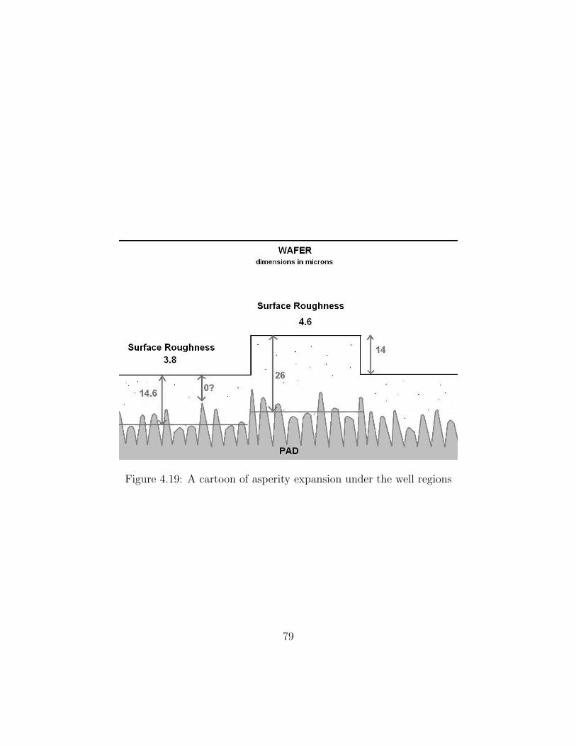
Figure 4.19: A cartoon of asperity expansion under the well regions
79

gest asperity compression outside the well, and the asperities have time to expand
under the wells as both surfaces rotate. Figure 4.20 shows that even though the
Ra fluctuates from image to image, the Ra inside the well is always larger than the
Ra outside the well. This supports the notion that the CMP polishing regime is of
partial lubrication. If it were true hydrodynamic lubrication, the roughness under
the wells would be the same as the rest of the pad.
Ra measurements were made using the wafer with 27 µm wells. The blue bars
in figure 4.21 is a histogram of the Ra measurements outside the well regions, and
the purple bars is a histogram of the Ra measurements inside the well regions. Ra
values inside the well seem to be centered at 4.6 µm, while outside the well they are
centered at 3.7 µm.
Measurements were taken with three different down-forces applied to the wafer
during polishing: 0.4, 1.8 and 3.2 psi. All Ra values at these down-forces were
within error of each other as shown in figure 4.22. Profilometer measurements of
the Freudenberg FX9 pad used during the runs indicate a pad Ra = 4.3 ± 0.3
µm. Comparing DELIF results in figure 4.22 to the profilometer measurements, we
may conclude that over this small ROI there is no significant additional asperity
compression during polishing as the down-force is increased. It is our belief that
the variations seen in successive DELIF images come from the wafer riding on waves
of slurry and passing over different pad global topography. The slurry flow to the
wafer is not smooth, due to the oscillating pad conditioner and global pad waviness
resulting in an unsteady bow wave at the leading edge of the wafer. This periodic
starving and feeding of the wafer means that at one instant the leading edge of the
80

Figure 4.20: The roughness values inside the well are greater than roughness outsidethe well
81

Figure 4.21: Histograms of roughness values inside and outside well regions
82

wafer could be digging into the pad, and the next instant it could be rising up as a
slurry wave passes below it. Previous modeling research [28] has shown that pressure
does vary locally beneath a wafer suggesting that we must interrogate a much larger
area under the wafer before we can draw any significant conclusion about Ra variation
with applied global down force.
Figure 4.23 shows Ra values from the three different regions of DELIF images with
air pockets inside the wells. Keep in mind that that the Ra measurements refer to
the slurry layer roughness and not the pad roughness. The roughness of the pad and
the slurry layer are the same when fluid completely fills the gap between a flat wafer
region and the pad. The Ra values of the slurry filled regions both inside and outside
the wells mirror the results from figure 4.23. Average Ra values for regions under the
air pockets are only slightly higher and in most cases are not significantly different
than Ra measurements in the slurry filled regions outside the wells. We believe the
air pockets are confined to the bottoms of the wells (above the pad asperities) in the
wafer with asperities sticking up beyond the fluid coverage within the air pockets. If
the air bubbles are shallow enough such that the asperity peaks are fully immersed,
then the measured roughness should match other areas under the wells.
4.2.3 Local Step Parameters
Much modeling research recently has focused on determining how the polishing pad
conforms to wafer features [31]. In a DELIF image if you choose to view a single
cross section over a step from an image such as in figure 4.24, the data displays a
lot of noise from the asperities. Rather than examining a single cross section, here
83

Figure 4.22: Surface roughness with increasing down-force during polishing
we examine the average of multiple cross section to determine how the fluid layer
and the pad are conforming to the steps in the wafer. Figure 4.25 shows two 14.5
µm deep 0.25 mm2 wells and their average of 50 cross section. Note that there is a
significant difference between the step heights (5 µm) for the wells even though they
are in the same image. The asperities seem to be sticking up higher on average in
the well on the right. This may be because of the global pad topography discussed
earlier or we may not be averaging over a large enough area.
In order to better characterize what the polishing pad is doing in the region
of the wafer step, we can fit the average cross section to an equation and analyze
the coefficients of that equation. The following analysis involves fitting single cross
section such as the one in figure 4.26. Once the average cross section is attained,
84

Figure 4.23: A comparison of roughness inside and outside the wells and underneathair pockets
85

Figure 4.24: A DELIF cross section across a wafer step
the data is recentered such that the steepest part of the step is at 0 on the x-axis.
The step can then be fit to equation 4.3 as in figure 4.27. It should be noted that
equation 4.3 has no physical significance, but it does happen to fit the data well.
y = btanh(ax) + cx + d (4.3)
The parameters a, b, c and d represent the following:
• a is the steepness of the step
• b is proportional to the average step height
• c is the slope of the wafer with respect to the pad
• d is the average slurry layer thickness at the midpoint of the step
86

Figure 4.25: Average cross section across two 27 µm deep wells on a FruedenbergFX9 pad
87

Figure 4.26: Average cross-section across a single wafer step 14.5 µm deep
88

Figure 4.27: An average cross section of a step fit to a sloped hyperbolic tangentcurve
89

Parameters a, b and c have been evaluated for all three step heights. Figure
4.28 shows a comparison of parameters a and b for the 3 steps. The y-axis is in
arbitrary units because all the data was normalized to the values of the 27 µm step
such that the parameters could be displayed on the same graph. The absolute value
of parameter b was evaluated because it can be positive or negative depending which
side of the step was evaluated. Parameter b seems to behave exactly as expected.
The difference in the slurry layer height from inside to outside the step decreases with
step height. While there seems to be some variation in the means of the steepness, a,
the standard deviations of these data seem to indicate that the values are all within
error.
Figure 4.29 shows the relative pad wafer angle across the step, parameter c, for all
three step heights. This angle can be affected both by global pad topography as well
as wafer stick-slip during polishing. Figure 4.29 indicates that this angle oscillates
with relatively the same amplitude for all three step heights. The data for the 5 µm
deep wells was taken on an FX9 pad with a sub-pad while the other two wafers were
run on FX9 pads without sub-pads. There seems to be no variation in wafer-pad
angles due to the sub-pad.
4.2.4 Asperity Compression
Two experiments will be discussed here. The first is a static case in which we compare
asperity compression and mean slurry film thickness due to applied down force. The
image of the 0 kPa was taken with the wafer sitting atop a conditioned Fruedenberg
FX9 pad and no shaft or lever arm pressure. The 0 kPa case was compared to a 70
90

Figure 4.28: Step fit parameters a (steepness) and b (step height) normalized to thevalues of the 27 µm deep wafer
91

Figure 4.29: Pad-wafer slope tracking (parameter c) over runs with different waferstep heights
92

kPa (10 psi) case in which the wafer was pressed against the pad in the same location
as the 0 kPa case. The second experiment was a dynamic case in which patterned
wafers were rotated against a conditioned Fruedenberg FX9 polishing pad.
For the static experiment, 17 different points on the pad were imaged at 0 and 70
kPa down-force. Figure 4.30 shows the histograms for one of these points on the pad
at the two down-forces. The 0 kPa case refers to images of the slurry layer under only
the weight of the wafer. Asperities are assumed to be minimally compressed in this
case because the histograms closely resemble Gaussian curves with minimal skew.
Histograms of images for the 70 kPa case exhibit skew towards darker intensities, or
a thinner slurry layer. Since the slurry completely fills the spaces between the wafer
and the polishing pad surface, the shape of the slurry layer thickness distribution
over an image should be the same as the asperity size distribution. Average asperity
compression over an image, (γ), due to the applied down force, can then be estimated
using the standard deviations of the slurry film thickness at 0 kPa and 70 kPa as
follows:
γ =σ − σ0
σ0
(4.4)
where (σ) and (σ0) are the standard deviations of the 70 kPa and 0 kPa cases,
respectively. By comparing the mean intensity values for the 70 KPa (µ70) and 0
kPa (µ0) images taken over the same portion of the polishing pad, the change in
slurry layer thickness, ∆δ,
∆δ = µ70 − µ0 (4.5)
93

can be calculated at that pad location.
The relationship between the means and the standard deviations of the his-
tograms at 0 kPa and 70 kPa should be related in some way because as the pressure
is increased, one would expect the amount of fluid in the viewing region to decrease
and the asperities should compress. In figure 4.31, the compression factor, γ, from
equation 4.4, is plotted on the x-axis and the and the change in slurry layer thick-
ness, ∆δ, from equation 4.5, is plotted on the y-axis. Each data point on the graph
represents the difference between 2 histograms (70kPa - 0kPa) as shown in figure
4.30. There are 17 total data points taken at 17 different locations on the polishing
pad under static conditions. Due to global pad topography, different amounts of fluid
are displaced around different parts of the pad. The fitted linear equation shown in
figure 4.31 with an R2 value of 0.7 shows that when more slurry is displaced, the
asperities are compressed more.
During the dynamic experiments, the down force applied to the etched wafers
was approximately 10 kPa. Figure 4.32 is an image of the slurry layer between
a patterned wafer with 27 µm deep wells and the pad. Means (µ) and standard
deviations, σ were determined for sub-images denoted by regions 1 and 2 labeled
in figure 4.32. The standard deviations for both regions were compare to evaluate
asperity compression from inside the patterned well to outside the well.
Figure 4.33 shows the distributions of the σ values in both regions for well depths
of 27 µm and 14.5 µm. In region 1, the σ value for both well depths is roughly the
same. However in region 2, the 27 µm deep wells have greater σ values than the
14.5 µm deep wells. The averages and standard deviations for all the data points
94

Figure 4.30: Histograms of DELIF intensities for a compressed and uncompressedpad
95
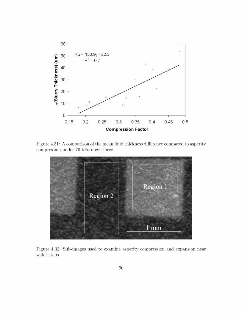
Figure 4.31: A comparison of the mean fluid thickness difference compared to asperitycompression under 70 kPa down-force
Figure 4.32: Sub-images used to examine asperity compression and expansion nearwafer steps
96

in figure 4.33 are shown in table 4.1. For both wafers, the asperities seem to be
expanding under the well, but the expansion is greater for deeper wells. Since the
surface roughness under the wells is approximately the same, the difference in the
distributions is probably not due to pad-wafer contact under the wells.
Table 4.1: Average value of asperity height, σ, and errors for dynamic image inregions 1 (R1) and 2 (R2)
Step Height R1 Avg R2 Avg27 µm 0.068±0.006 0.083±0.008
14.5 µm 0.063±0.004 0.072±0.007
Another way of looking at asperity compression under dynamic conditions is
shown in figure 4.34. Figure 4.34 shows the amount of asperity compression relative
to wafer step height. In the case of the 14.5 µm and 5 µm deep wells, some of the
compression factors calculated were negative. There were quite a few more negative
values of compression in the 5 µm case than the 14.5 µm case. It is unlikely that
the asperities are expanding when they travel from inside to outside the wells, so
these negative values of the compression factor most likely mean that there is close
to zero expansion under the wells for those images. The dashed lines on this graph
indicate the height of the wells in the wafer. In the 14.5 µm and 27 µm case, there is
a significant separation between the average slurry thickness line (solid) and the line
wafer height (3-4 µm). This difference can be thought of as the asperity expansion
distance. In the 5 µm case, the slurry film thickness line is within error of the wafer
height line, also supporting the idea that there is minimal asperity expansion in these
shorter wells. The asperities may actually be in contact with the tops of the 5 µm
97

Figure 4.33: A comparison of standard deviations of intensity inside and outside wellregions for the 14.5 µm and 27 µm deep wells
98

wells.
99
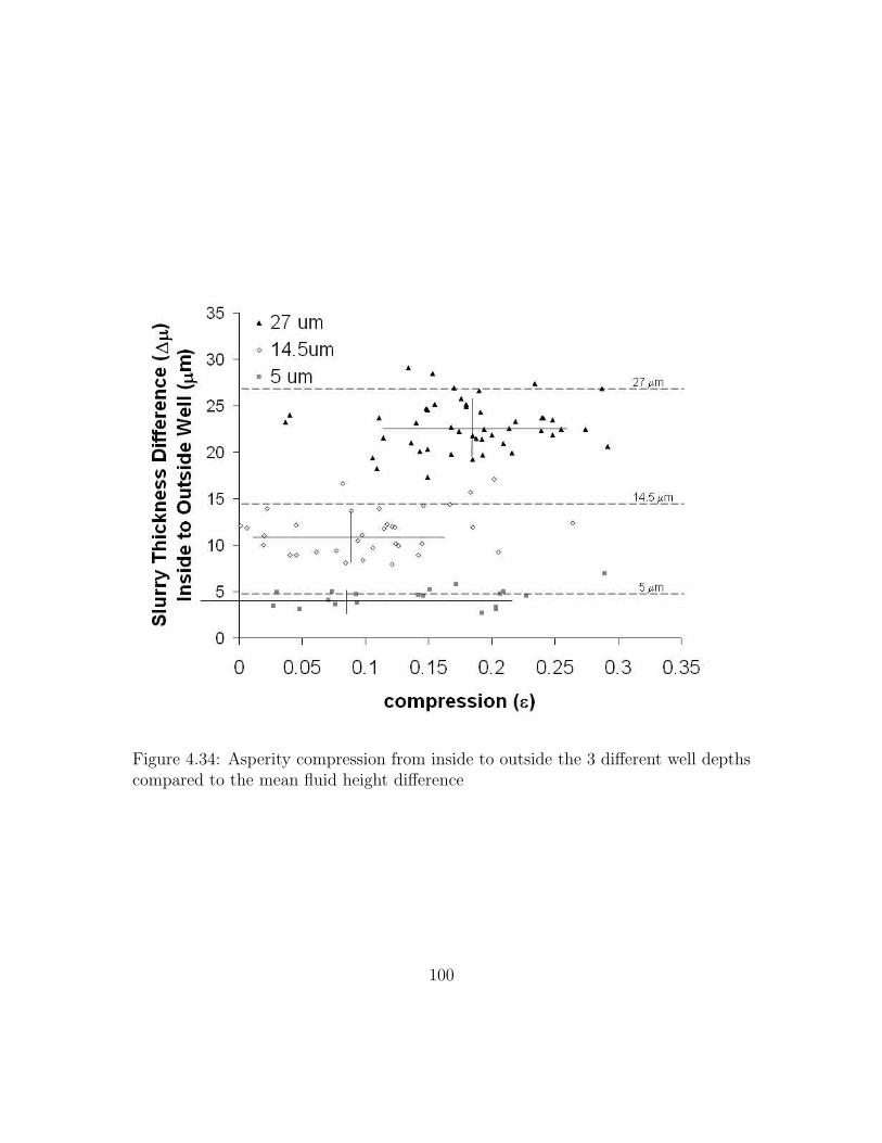
Figure 4.34: Asperity compression from inside to outside the 3 different well depthscompared to the mean fluid height difference
100

Chapter 5
Summary, Conclusions and Future
Work
The DELIF technique has been modified such that the slurry layer thickness can
be attained at a rate of 2 images per second during CMP at pad asperity scale
resolution. In situ images are taken at a frequency of 2 Hz over an area of 1.6 x
2.7 mm. The fluid layers were observed between the patterned wafers and several
types of polishing pads that are commercially available and in development. Both a
qualitative and quantitative analysis of these images has been provided. This chapter
will summarize the results and present future research directions.
5.1 Setup Modifications
We have made multiple modifications to polishing tool to acheive more consistent
polishing parameters. The modifications include
101
1. integration of a force transducer table,
2. replacement of the drill press with a simple aluminum shaft,
3. lowering the center of wafer rotation, and
4. simplifying in-situ conditioning.
In addition to tool modification, the optical acquisition of DELIF images has been
modified. Instead of dissolving 2 dyes in the slurry and suppressing the fluorescence
of the polishing pad, we use the pad fluorescence to excite one dye in the slurry.
Integration of a laser has enabled a sampling rate of 2 images/s. The new Evolution
VF cameras have more than 1.4 megapixels and are capable of resolving 4096 gray
levels. Separation of the zoom lens from the CCD element has increased image
resolution tenfold.
5.2 Experimental Conclusions
DELIF images were acquired and analyzed for several different types of polishing
pads. The ability to resolve wafer features is limited by pad topography. Most
of the research was done on Fruedenberg FX9 polishing pads, which are similar
to the industrial standard Rodel IC1000 polishing pads. These pads have a surface
roughness of approximately 4.6 µm and exhibit striations due to in-situ conditioning.
With these pads, it is possible to resolve wafer features as small as 5 µm in depth
and 22 µm in width. Deeper wells led to air pockets underneath wafer features and
102

over both flat and grooved pads. With grooved pads, air pockets are confined to the
grooves.
By calculating a relative calibration factor, it is possible to estimate asperity
compression during polishing. This calibration factor allows us to examine slurry
film roughness, slurry layer thickness changes near steps in the wafer, and asperity
compression and expansion under the wafer.
While surface roughness was not observed to vary with global applied down-
forces, roughness was observed to vary beneath 27 um deep etched wafer features.
Observation of slurry layer roughness beneath air pockets within the wafer features
show that the slurry does not completely fill the regions between asperities when
air is trapped under the wafer. The data presented here support the idea that a
wafer and pad are in partial contact (the mixed lubrication regime) during a CMP
polishing run.
Step heights can be characterized by fitting the average cross section across a
step to a hyperbolic tangent curve. Linear parameters were added to the hyperbolic
tangent curve because the wafer-pad angle varies during dynamic runs. The average
steepness of the steps seemed to decrease with step height, but variation in the
data was so large that the steepness value for all three step heights were within
experimental error. The variation in pad-wafer angle was the same for all three
step heights meaning that the pad-wafer angle is independent of patterns within this
range (5-27 µm).
Global pad topography results in widely varying fluid displacement due to applied
down-forces to the wafer over small areas (6 mm2). Analysis of asperity compression
103

in static images after applying 70 kPa down-force shows that average asperity com-
pression increases with the reduction of the average slurry layer thickness. Dynamic
measurements show that asperity expansion increases with well depth.
5.3 Future Research Directions
While many of the modifications to the setup and DELIF procedure have proven
beneficial, there is still room for optimization of the technique. Spectral analysis
of DELIF components shows that Calcein may not be the most optimal thickness
dependent dye to use when relying on the polishing pad as an excitation source. We
either need to develop a correction technique for the ratio drift in time or choose a
more optimal dye. If a different dye is chosen, the filters and beam-splitter system
should be reevaluated.
The incorporation of a force table has allowed us to more accurately measure
down forces in addition shear forces and moments about all three axes. While this
device was not used to a large degree in this work, it has great potential to be used
to correlate pad-wafer contact from DELIF images to stick-slip phenomena. In order
to compare global down forces applied to the wafer to polishing pad deformation and
asperity compress, it is necessary to acquire images over an entire half of the wafer
instead of a 6mm2 region. Since our current calibration is only accurate to within a
micron or so, and we rarely observe fluid layer thicknesses greater than 100 µm on a
flat polishing pad, it may be worth investing in lower gray-scale resolution cameras
(8 or 10 bit) that have more pixels. With our current setup it may only be possible to
104

increase the viewing region without sacrificing spacial resolution by eliminating the
camera binning. This would quadruple the viewing area. Finally, if the ratio value
at the point of pad-wafer contact (the intensity value of zero slurry film thickness)
can be determined, we can obtain an absolute calibration of the images.
105

Bibliography
[1] J M Steigerwald, S P Murarka, and R J Gutmann. Chemical Mechanical Pla-
narization of Microelectronic Materials. John Wiley and Sons, Inc., 1997.
[2] M A Fury. The early days of cmp. Solid State Technology, 40:81–86, 1997.
[3] The international technology roadmap for semiconductors 2001 edition. Tech-
nical report, Semiconductor Industry Association (SIA), San Jose, CA, 2001.
[4] D G Thakurta, C L Borst, D W Schwendeman, R J Gutmann, and W N Gill.
Pad porosity, compressibility and slurry delivery effects in chemical mechanical
planarization: Modeling and experiments. Thin Solid Films, 336:181–190, 2000.
[5] D O Ouma, D S Boning, J E Chung, W G Easter, V S Saxena, S Misra, and
A Crevasse. Characterization and modeling of oxide chemical-mechanical polish-
ing using planarization length and pattern density concepts. IEEE Transactions
on Semiconductor Manufacturing, May 2002.
[6] S R Runnels, F Miceli, and I Kim. Validation of a large area three-dimensional
erosion simulator for chemical mechanical polishing. Journal of the Electrochem-
ical Society, 146(12):4619–4625, 1999.
106

[7] W T Tseng and Y L Wang. Re-examination of pressure and speed dependencies
of removal rate during chemical mechanical polishing process. Electrochemical
Society Letters, 144(2):L15–L17, 1997.
[8] B Mullany and G Byrne. The effect of slurry viscosity on chemical-mechanical
polishing of silicon wafers. Journal of Materials Processing Technology, 132:28–
34, 2003.
[9] J Coppeta and C Rogers. Mixing measurements using laser induced fluorescence.
American Institute of Aeronautics and Astronautics, 1994. Paper no. 95-0167.
[10] J Coppeta and C Rogers. Dual emission laser induced fluorescence for direct
planar scalar behavior measurements. Experiments in Fluids, 25:1–15, 1998.
[11] M J Madou. Fundamentals of Microfabrication: The Science of Miniaturization,
chapter 1-5. CRC Press LLC, 2nd edition, 2002.
[12] L Trotha, G Morsch, and P Wolters. Advances in mems fabrication using cmp.
Semiconductor International, August 1:54, 2004.
[13] R Wilson and D Lammers. Heavy rules hold back 90-nm yield. EE Times
Online, March 28 2005.
[14] J M Rabaey. Digital Integrated Circuits: A Design Perspective. Pearson Edu-
cation, 2nd edition, 2003.
[15] D Rosales-Yeomans, T Doi, M Kinoshita, T Suzuki, and A Philipossian. Effect
of pad groove design on the frictional and removal rate characteristics of ild
cmp. Journal of the Electrochemical Society, 152:G62–G67, 2005.
107

[16] J C Lu. Fluid film lubrication in chemical mechanical planarization. Master’s
thesis, Tufts University, 2001.
[17] W Choi, S M Lee, and R K Singh. ph and down load effects on silicon dioxide
dielectric cmp. Electrochemical and Solid State Letters, 7:G141–G144, 2004.
[18] W Choi, S M Lee, J Abiade, and R K Singh. Estimation of fractional surface
coverage of particles for oxide cmp. Journal of the Electrochemical Society,
151:G368–G372, 2004.
[19] A Philipossian and S Olsen. Effect of slurry flow rate on pad life during interlayer
dielectric cmp. Journal of the Electrochemical Society, 151:G436–G439, 2004.
[20] J T Cornely. Thermal characteristics of chemical mechanical planarization.
Master’s thesis, Tufts University, 2002.
[21] H Hocheng, Y L Huang, and l J Chen. Kinematic analysis and measurement of
temperature rise on a pad in chemical mechanical planarization. Journal of the
Electrochemical Society, 146(11):4236–4239, 1999.
[22] H J Kim, H Y Kim, H D Jeong, E S Lee, and Y J Shin. Friction and thermal
phenomena in chemical mechanical polishing. Journal of Materials Processing
Technology, 130-131:334–338, 2002.
[23] H Ogawa, M Yanagisawa, J Kikuchi, and Y Horiike. Study on the mechanism
of silicon chemical mechanical polishing employing in situ infrared spectroscopy.
Japanese Journal of Applied Physics Part 1, Regular Papers Short Notes and
Review Papers, 42:587–592, 2003.
108

[24] S R Runnels and L M Eyman. Tribology analysis of chemical-mechanical pol-
ishing. Journal of the Electrochemical Society, 141(6):1698–1701, 1994.
[25] S Sundararajan, D G Thakurta, D W Schwendeman, S P Murarka, and W N
Gill. Two-dimensional wafer-scale chemical mechanical planarization models
based on lubrication theory and mass transport. Journal of the Electrochemical
Society, 146(2):761–766, 1999.
[26] J M Chen and Y C Fang. Hydrodynamic characteristics of the thin fluid film
in chemical-mechanical polishing. IEEE Transactions on Semiconductor Man-
ufacturing, 15(1):39–44, February 2002.
[27] X Jin, L M Keer, and Q Wang. A 3d ehl simulation of cmp. Journal of the
Electrochemical Society, 152(1), 2005.
[28] C F Higgs III, S H Ng, L Borucki, I Yoon, and S Danyluk. A mixed-lubrication
approach to predicting cmp fluid pressure modeling and experiments. Journal
of the Electrochemical Society, 152(3):G193–G198, 2005.
[29] D G Thakurta, C L Borst, D W Schwendeman, R J Gutmann, and W N Gill.
Three-dimensional chemical mechanical planarization slurry flow model based
on lubrication theory. Journal of the Electrochemical Society, 148:G207–G214,
2001.
[30] A F Scarfo. Fluid flow analysis of the chemical mechanical planarization process.
Master’s thesis, Tufts University, 2002.
109

[31] S Taylor. Numerical simulation of pad-wafer interaction in chemical mechanical
planarization. Master’s thesis, Tufts University, 2004.
[32] J R Coppeta. Investigating Fluid Behavior Beneath a Wafer During Chemical
Mechanical Polishing Process. PhD thesis, Tufts University, 1999.
[33] E Y Chan. Instantaneous mapping in chemical mechanical planarization. Mas-
ter’s thesis, Tufts University, 2003.
[34] J Coppeta and C Rogers. A quantitative mixing analysis using fluorescent dyes.
American Institute of Aeronautics and Astronautics, 1995. Paper no. 96-0539.
[35] J Coppeta, C Rogers, A Philipossian, and F B Kaufman. A technique for mea-
suring slurry-flow dynamics during chemical-mechanical polishing. Materials
Research Society Proceedings, Symposium L, Fall 1996.
[36] J Coppeta, C Rogers, A Philipossian, and F B Kaufman. Characterizing slurry
flow during CMP using laser induced fluorescence. Proceedins of the Second
International Chemical Mechanical Polish Planarization for ULSI Multilevel In-
terconnection Conference, pages 307–314, February 13-14 1997.
[37] J Coppeta, C Rogers, L Racz, A Philipossian, and F B Kaufman. A statistical
analysis of key parameters in slurry transport beneath a wafer during chemical-
mechanical polishing. Journal of C.M.P. for ULSI Multilevel Interconnection,
1(1):47–60, 1999.
[38] J Coppeta, C Rogers, L Racz, A Philipossian, and F B Kaufman. Investigating
110

slurry transport beneath a wafer during chemical mechanical polishing process.
Journal of the Electrochemical Society, 147(5):1903–1909, 2000.
[39] J Coppeta, C Rogers, L Racz, A Philipossian, and F B Kaufman. The influ-
ence of CMP process parameters on slurry transport. Proceedings of the Fourth
International Chemical Mechanical Polish Planarization for ULSI Multilevel In-
terconnection Conference, pages 37–44, February 11-12 1999.
[40] J Coppeta, L Racz, A Philipossian, F B Kaufman, and C Rogers. Pad effects
on slurry transport beneath a wafer during polishing. Proceedings of the Third
International Chemical Mechanical Polish Planarization for ULSI Multilevel In-
terconnection Conference, pages 36–43, February 19-20 1998.
[41] C Rogers, J Coppeta, L Racz, A Philipossian, F B Kaufman, and D Bramono.
Analysis of flow between a wafer and pad during CMP processes. Journal of
Electronic Materials, 27(10):1082–1087, 1998.
[42] J Cornely, C Rogers, V Manno, and A Philipossian. In situ temperature mea-
surement during oxide-chemical mechanical planarization. Proceedings for the
MRS Spring Meeting, Santa Clara, CA, 2003.
[43] J Lu, C Rogers, V Manno, A Philipossian, S Anjur, and M Moinpour. Mea-
surements of slurry film thickness and wafer drag during cmp. Journal of the
Electrochemical Society, 151, 2004.
[44] C Gray, D Apone, C Rogers, V P Manno, C Barns, M Moinpour, S Anjur,
111

and A Philipossian. Viewing asperity behavior under the wafer during cmp.
Electrochemical and Solid State Letters, 8:G109–G111, 2005.
[45] D Apone. Instantaneous fluid film imaging in chemical mechanical planarization.
Master’s thesis, Tufts University, 2005.
[46] C H Hidrovo and D P Hart. Emission reabsorption laser induced fluorescence (er-
lif) film thickness measurement. Measurement Science and Technology, 12:467–
477, 2001.
[47] J Sakakibara and R J Adrian. Whole field measurement of temperature in water
using two-color laser induced fluorescence. Experiments in Fluids, 26:7–15, 1999.
[48] J Sakakibara and R J Adrian. Measurement of temperature field of a rayleigh-
benard convection using two-color laser-induced fluorescence. Experiments in
Fluids, 37:331–340, 2004.
[49] H Inagaki, A Saito, M Murakami, and T Konomi. Measurement of oil film thick-
ness distribution on piston surface using the fluorescence method (development
of measurement system). Japan Society of Mechanical Engineers, International
Journal, 40:487–493, 1997.
[50] D A McQuarrie and J D Simon. Physical Chemistry: A Molecular Approach,
chapter 15, pages 591–619. University Science Books, 1997.
[51] R P Haugland. Handbook of Fluorescent Probes and Research Chemicals. Molec-
ular Probes, Eugene, OR, 7th edition, 1999.
112