
ME395 Final Project: Problem Statement Szu-Kang...
52
ME395 Final Project: Manuscript Szu-Kang Hsien Ayodeji O. Coker 1. Name of the Project: From Ink-Jet Technology to Nano Array Writing Technology Since Ink-jet micromaching technology has been introduced 30 years ago, the ink jet printer has emerged as one of the mainstream printing technologies. From its market inception in 1985, the Hewlett Packard’s thermal ink jet technology has evolved progressively from a 12 nozzle 96 dpi (dots per inch) to a 300 nozzle 600 dpi print head [1]. Recently Epson introduced its modified micro piezoelectric printer, which has 1400 dpi resolution. Based on the micro piezoelectric printer technology and the new “Dip-Pen” Nanolithography technology, we come up with a design called “Nano Array Writing” that can write a resolution of 30 nm linewidth continuously. 2. Objective: Using nanotechnology and microfabrication techniques to manufacture so-called “Nano Array Writing” to produce very 1
Transcript of ME395 Final Project: Problem Statement Szu-Kang...
ME395 Final Project: Manuscript Szu-Kang Hsien
Ayodeji O. Coker
1. Name of the Project:
From Ink-Jet Technology to Nano Array Writing Technology
Since Ink-jet micromaching technology has been introduced 30 years ago, the ink jet
printer has emerged as one of the mainstream printing technologies. From its market
inception in 1985, the Hewlett Packard’s thermal ink jet technology has evolved
progressively from a 12 nozzle 96 dpi (dots per inch) to a 300 nozzle 600 dpi print head
[1]. Recently Epson introduced its modified micro piezoelectric printer, which has 1400
dpi resolution. Based on the micro piezoelectric printer technology and the new “Dip-
Pen” Nanolithography technology, we come up with a design called “Nano Array
Writing” that can write a resolution of 30 nm linewidth continuously.
2. Objective: Using nanotechnology and microfabrication techniques to manufacture so-called
“Nano Array Writing” to produce very thin linewidth (30nm) to replace the traditional
lithography tools. One of the goals of this project is to create a process whereby we can
control individually an array of AFM tips. We propose the use of a process developed by
N.C Macdonald et al., in which the integration of micro-actuators and nanometer-scale
tips (the AFM tip in our case) was employed to control things on a small scale.
3. Approach and literature review: Due to the large demand of high speed microprocessors and large capacity of memory
chips, the gate length of transistors need to shrink down in order to keep up with the pace.
According to Moore’s Law, the number of transistors capable of being put on a processor
should double every 18 months. So in order to keep with the demand, manufacturers need
to find reliable and cheap lithography sources that can generate smaller wavelength every
1
two or three years. Right now, manufacturers are using deep UV excimer laser (DUV)
lithography tools to produce 0.1 m linewidth on top of the wafer but unfortunately, the
current technique will likely hit its limit around 2003. There are many candidates that can
write even smaller linewidth for examples X-ray, E-beam and the most recently talked
about extreme ultra-violet (EUV) lithography onto a wafer, but X-ray and E-beam are not
cost-effective and the EUV technology can only write down to 70nm. So we came up
with a design that can combine the more established ink-jet technology to provide the ink
and the traditional Atomic Force Microscopy (AFM) tips to write very small linewidth
directly on the wafer without using the traditional lithography methods. First we like to
talk about the revolution of printing technology from laser to ink-jet and secondly, the
theory, operation of AFM and the fabrication of its silicon nitride tip and thirdly, using
micromaching comb-drive actuators to control the x, y, z direction of the tip, and fourth,
the dip pen technology and surface chemistry behind the writing and finally the structure
of our newly designed devices.
1. Revolution of Printing:Laser Printer:
The technology behind color laser printer is electrophotography or xerography and it
was the invention of one man, Chester Carlson in 1938. The two ideas that he brought
together were: the formation of an electrostatic latent image using photoconductivity
to selectivity discharge a surface charged insulator, and “development” of this latent
image by dusting with powers charged electrostatically. No chemical reaction are
involved in processing. It is essential a dry photoelectric process. Unlike silver
emulsions, the xerographic plate is not necessarily consumed in processing. The plates
can be used over and over again for hundreds or even thousands of exposures. Since the
first machine introduced 40 years ago by Xerox Corporation, technology has been
improved.
Generally, six steps are involved in making a print by xerography [2], as we can see in
Figure 1:
1. Sensitizing the xerographic plate by electrical charging.
2. Exposing the plate to form a latent electrostatic image.
2
3. Developing the latent image with fine particles.
4. Transferring the developed image to paper or other materials.
5. Fixing the image by fusing, and
6. The plate is discharged, cleaned, and reused.
Laser printers have been growing very fast in the last 20 years and will continue be the
dominant player in the high-end market segment. This is because printers based on
electrophotographic are quiet and fast output, can handle multiple fonts, can produce
pictorial information over a wide speed range, and can produce very good and vivid
pictures. Even though Canon introduced the replacement cartridge concept and used
cheap semiconductor laser in 1983, the price is still quite high for household users.
Usually the price color laser printer is 5-10 times higher than the ink-jet printer but the
gap has been narrowed quite fast.
Ink-Jet Printer:
Inkjet printing has become recognized as a prominent contender in the digitally
controlled, electronic printing arena because of its non-impact, low-noise characteristics,
good printing quality at reasonable cost, color capability and versatility, its use of plain
paper and its avoidance of toner transfers and fixing. Many types of ink jet printing
mechanisms have been invented. These can be categorized as either continuous ink jet
(CIJ) or drop on demand (DOD) ink jet [3], as we can see from Table 1.
Continuous ink jet printing dates back to at least 1929, where Hansell discloses an
array of continuous ink jet nozzles where ink drops to be printed are selectively charged
and deflected towards the recording medium. This technique is known as binary
deflection Continuous ink jet and is used by several manufacturers, including Elmjet and
Scitex. Hertz et al published a U.S. patent no. 3,416,153, in 1966 [4], discloses a method
of achieving variable optical density of printed spots in CIJ printing using the
electrostatic dispersion of a charged drop stream to modulate the number of droplets
which pass through a small aperture. This technique is used in ink jet printers
manufactured by Iris Graphics. Recently in 1994, L. Smith et al published a paper in
Sensor and Actuators A [5] discussing the Continuous Ink Jet technology has an edge
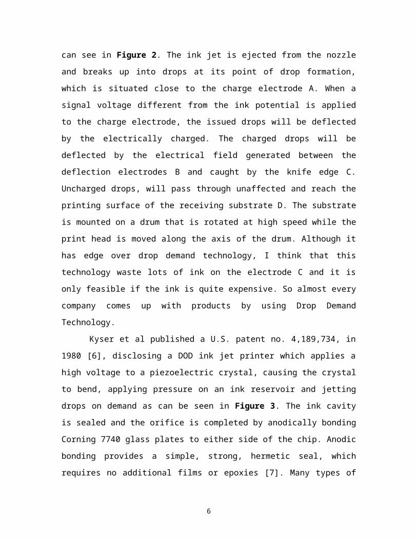
over the DOD with respect to high quality printing, as we can see in Figure 2. The ink jet
3
is ejected from the nozzle and breaks up into drops at its point of drop formation, which
is situated close to the charge electrode A. When a signal voltage different from the ink
potential is applied to the charge electrode, the issued drops will be deflected by the
electrically charged. The charged drops will be deflected by the electrical field generated
between the deflection electrodes B and caught by the knife edge C. Uncharged drops,
will pass through unaffected and reach the printing surface of the receiving substrate D.
The substrate is mounted on a drum that is rotated at high speed while the print head is
moved along the axis of the drum. Although it has edge over drop demand technology, I
think that this technology waste lots of ink on the electrode C and it is only feasible if the
ink is quite expensive. So almost every company comes up with products by using Drop
Demand Technology.
Kyser et al published a U.S. patent no. 4,189,734, in 1980 [6], disclosing a DOD ink
jet printer which applies a high voltage to a piezoelectric crystal, causing the crystal to
bend, applying pressure on an ink reservoir and jetting drops on demand as can be seen in
Figure 3. The ink cavity is sealed and the orifice is completed by anodically bonding
Corning 7740 glass plates to either side of the chip. Anodic bonding provides a simple,
strong, hermetic seal, which requires no additional films or epoxies [7]. Many types of
piezoelectric drop on demand printers have subsequently been invented, which utilize
piezoelectric crystals in bend mode, push mode, shear mode, and squeeze mode.
Piezoelectric DOD printers have achieved commercial success using hot melt inks (for
example, Tektronix and Dataproducts printers), and at image resolutions up to 1440 dpi
for home and office printers (Seiko Epson). Piezoelectric DOD printers have an
advantage in being able to use a wide range of inks. However, piezoelectric printing
mechanisms usually require complex high voltage drive circuitry and bulky piezoelectric
crystal arrays, which are disadvantageous in regard to manufacturability and
performance.
Endo et al published a British patent no. 2,007,162, in 1979 [8], disclosing an
electrothermal DOD ink jet printer which applies a power pulse to an electrothermal
transducer (heater) which is in thermal contact with ink in a nozzle. The heater rapidly
heats water-based ink to a high temperature, whereupon a small quantity of ink rapidly
evaporates, forming a bubble. The formation of these bubbles results in a pressure wave,
4

which cause drops of ink to be ejected from small apertures along the edge of the heater
substrate. This technology is known as Bubblejet.TM. (Trademark of Canon of Japan),
and is used in a wide range of printing systems from Canon, Xerox, and other
manufacturers and the ink flow comes out from the side of the shooting chamber which is
also called the Sideshooter Ink-Jet as can be seen in Figure 4.
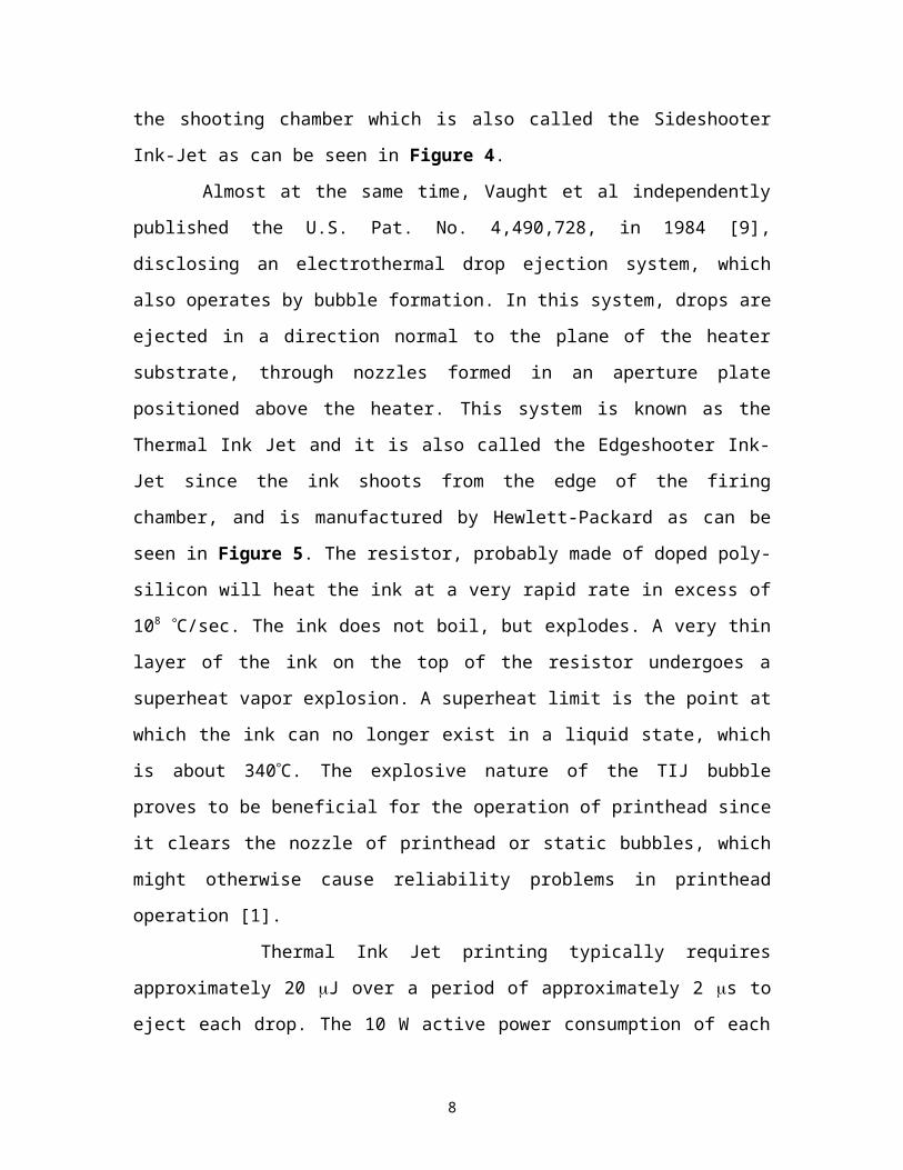
Almost at the same time, Vaught et al independently published the U.S. Pat. No.
4,490,728, in 1984 [9], disclosing an electrothermal drop ejection system, which also
operates by bubble formation. In this system, drops are ejected in a direction normal to
the plane of the heater substrate, through nozzles formed in an aperture plate positioned
above the heater. This system is known as the Thermal Ink Jet and it is also called the
Edgeshooter Ink-Jet since the ink shoots from the edge of the firing chamber, and is
manufactured by Hewlett-Packard as can be seen in Figure 5. The resistor, probably
made of doped poly-silicon will heat the ink at a very rapid rate in excess of 108 C/sec.
The ink does not boil, but explodes. A very thin layer of the ink on the top of the resistor
undergoes a superheat vapor explosion. A superheat limit is the point at which the ink can
no longer exist in a liquid state, which is about 340C. The explosive nature of the TIJ
bubble proves to be beneficial for the operation of printhead since it clears the nozzle of
printhead or static bubbles, which might otherwise cause reliability problems in printhead
operation [1].
Thermal Ink Jet printing typically requires approximately 20 J over a period of
approximately 2 s to eject each drop. The 10 W active power consumption of each
heater is disadvantageous in itself and also necessitates special inks, complicates the
driver electronics and precipitates deterioration of heater elements. But as we can see
from Figure 6, with the combination of higher firing frequency and more nozzles in the
TJI printhead results in very high print speed and it continues to outpace piezoelectric ink
jet [1]. The superiority of TJI in print speed can now rival that of laser printers. The
recently announced HP 2000C can print full-page color documents in about 43 second-
other inkjet and laserjet printers take two minutes.
Other ink jet printing systems have also been described in technical literature, but are
not currently used on a commercial basis. For example, U.S. Pat. No. 4,275,290 discloses
a system wherein the coincident address of predetermined print head nozzles with heat
5
pulses and hydrostatic pressure, allows ink to flow freely to spacer-separated paper,
passing beneath the print head. U.S. Pat. Nos. 4,737,803, 4,737,803 and 4,748,458
disclose ink jet recording systems wherein the coincident address of ink in print head
nozzles with heat pulses and an electrostatically attractive field cause ejection of ink
drops to a print page. P. Krause et at of Germany in 1994 think of using <110> silicon
wafer to produce “Backshooter” ink jet system that can reduce the manufacturing costs
since it reduce large number of electrical interconnections [10] (at least one nozzle plus a
common rear conductor), as in Figure 7. But I think that the price of its printer head will
be high compared to “Edgeshooter” by HP and “Sideshooter” by Canon since it is using
<110> silicon wafers
Each of the above-described inkjet printing systems has advantages and
disadvantages. However, there remains a widely recognized need for an improved ink jet
printing approach, providing advantages for example, as to cost, speed, quality,
reliability, power usage, simplicity of construction and operation, durability and
consumables.
2. Piezoelectricity: Piezoelectric properties of a medium can be explained by the concept of
piezoelectricity, which determines the distribution of the electric polarization and
demonstrates how a piezoelectric field reacts to an electrical stress by emitting
depolarization waves. The polarization field is linear with respect to mechanical strain in
crystals belonging to certain symmetry classes. If there is no external field, crystal strain
force is balanced by the internal polarization force. When this equilibrium is disturbed by
the external field or mechanical force, the emitting depolarization field will create a
rebalance force to maintain the initial equilibrium. If the external field is electrical field, a
displacement will occur, but if the external force is from mechanical displacement, an
electrical field will be produced. This is called the piezoelectricity. Table 2 lists several
different kinds of piezoelectricity materials. Changing in voltage, gives rise to a
corresponding force, F, and the resulting dimensional change L as we can see below:
V=Q/C=Qx/(orA) V=dijFjx/(orA)
6

Typically values for L vary between 10-10 and 10-7 cm/V. Thus, to obtain
displacements on the order of m, voltages need to exceed 1000 V, unless stacked
actuators or mechanical motion amplification methods are used [10].
For crystalline quartz, the piezoelectric can be written as:
d11 d12 0 d14 0 0
dik= 0 0 0 0 0 0
0 0 0 0 0 0
We can assume that our PZT film is about 2 m, and the voltage added on this thin
film can’t exceed 10 V since the break down electric field is around 5000 (V/mm) and in
more humid environment this break down field will be even lower. Using the equation
above we can get F will be 0.11 N (PZT film dimension 100m*100m, r=3000,
d11=370 pC/N, d31=110 pC/N). And the displacement of the crystal, L= LV/(td31), will
be around 0.2m. So we can stack around 5 PZT crystals together in order to have 1m
pressing into the ink. The pressure applying to the liquid can be up to 107 N/m2 or
approximately 100 pounds per square inch.
They are many piezoelectric film reported in the last 20 years. The three most popular
with the sensor industry are ZnO, AlN and Pb(Zr,Ti)O3 (PZT) Thin films. Because PZT
has high piezo-coupling, high piezoelectric constant and very high dielectric constant
compared to ZnO and AlN, there have been enormous papers on this material. Many
methods and techniques have been reported such as e-beam evaporation, RF sputtering,
ion-beam deposition, MOCVD, magnetron sputtering and sol-gel. In our device, we can
choose e-beam evaporation or RF sputtering because the equipment is quite convenient.
3. AFM working methods and the fabrication of its tip: In 1981, Dr. Gerd Binning and his colleagues at IBM Zurich Research Laboratory
developed the first scanning tunneling microscope (STM) that is the first instrument
capable of directly obtaining three-dimensional images of solid surfaces with atomic
resolution. But the STM can only study surfaces, which are electrically conductive to
some degree. Based on this design, Binning et al. developed an atomic force microscope
(AFM) to measure ultra-small forces (less than 1 N) between the AFM tip and the
sample surface. AFMs can be used to measure all kinds of surface either conducting or
7
insulating. AFM then become a very popular surface profiler for topographic
measurements on micro-to nanoscale [11].
Like the STM, the AFM relies on a scanning technique to produce very high
resolution, three-dimensional images of sample surfaces. AFM uses the motion of a very
flexible cantilever beam with low vertical spring constant (0.05 to 1 N/m) and a very
small mass (on the order of 1 mg) to measure the ultra-small force between the AFM tip
and sample surface. The AFM combines the principles of the STM and the stylus profiler
as shown in Figure 8. Usually the tip is only a couple of microns long and often less than
10 nm in diameter at the end and the cantilever is about 100-200 m. Today the most
advanced tip can be microfabricated from silicon nitride using photolithography
techniques, as we will discuss below. The lever deflection has been measured by several
different methods including capacitance-detection, optical interferometry detecting and
laser beam deflection. And I think that by using the capacitance-deflection, we can
control which AFM will go down to the surface and write the linewidth.
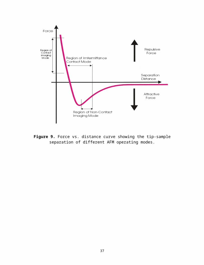
Generally, there are three types of methods the AFM used to measure the profile of
the surface, one is the “repulsive mode” or “contact mode”, the second one is the
“intermittent-contact mode”, and the last one is the “attractive force imaging” or “non-
contact imaging” as we can see from Figure 9 [12]
A. Contact Mode
Conceptually, contact mode is the most straightforward AFM imaging mode. The
cantilever tip is held close to the sample surface and the sample surface rastered
underneath the tip. As the sample surface is moved, the change in topography results in a
change in tip-sample interaction. Thus, the force incident on the cantilever tip is altered
and the equilibrium between the elastic force of the deflected cantilever and applied force
changed. The AFM operates in either constant height or constant force mode. The
constant force mode is generally the preferred mode of operation. The total force exerted
by the tip on the sample being within the limits. However, the response time is quite slow
and it affects the scanning speed.
B. Non-contact Mode
Non-contact AFM is one of several vibrating cantilever techniques in which an AFM
cantilever is vibrated near the surface of the sample. The cantilever is held 5-10 nm away
8
from the surface, within the region where long-range Van Der Waals forces dominate.
Although the attractive force imaging exerts no normal pressure at the interface, the
scanning speed is slow and the main disadvantage is that in humid conditions the tip will
condense water so this method is seldom used outside the research environments.
C. Intermittant-Contact Mode
Intermittent contact AFM is a hybrid of contact and non-contact systems. The
cantilever beam is also vibrated, but the distance is held at a tip-sample closer than the
non-contact AFM so that the tip just touches or taps the sample surface. And the lateral
forces (frictional or drag) are reduced so it is less unlikely to damage the surface of soft
samples as in the contact mode case. IC-AFM has become an important AFM technique
since it overcomes some of the limitations of both contact and non-contact AFM.
The key to the successful operation of an AFM is the measurement of the interaction
forces between the tip and the sample surface. The tip would ideally be just one atom, but
it is not feasible. Typically, the interaction forces between the AFM tip and the sample
surface must be smaller than about 10-7 N for bulk materials and preferably well below
10-9 N for organic materials. Experience shows that cantilevers with spring constants
about 0.01 N/m work best in liquid environments like in our DIP condition. To obtain a
measurable deflection it needs to be at least 10 nm to overcome the noise and thermal
drift. So we can see that Si3N4 is a good candidate.
The method of making cantilevers with integrated tips of Si3N4 is briefly described in
Albrecht et al. paper [13]. The process starts with a Si (100) wafer with a thermally
grown SiO2 layer, as shown in Figure 10. The steps are follows:
1. Using a photolithographic method, etch a square opening on the SiO2 film.
2. Use KOH solution to etch the part of the silicon wafer exposed through the square
opening. The etch self-terminates at the Si (111) planes, and a pyramidal pit is
formed.
3. Remove the SiO2 protection layer.
4. Deposit Si3N4on the wafer, to form the shape of the cantilever using a lithographic
method.
5. Attach a piece of glass as the carrying substrate using anodic bonding. A Cr layer
on the glass protects the area with the cantilever.
9
6. Remove the unwanted part of glass and all the remaining Si.
7. The wafer is diced into pieces. Each piece is a small glass block with several
cantilevers attached to its edges.
Figure 11 is a micrograph of a tip with this process. There are several reasons
choosing silicon nitride film. First, the film is robust and inert. Second, the tip sidewalls
are extremely smooth and have a slope of 550, which facilitates low friction sliding over
rough surfaces. Third, the effects of tip morphology on the image can be understood and
taken into account. Typically the force constant of silicon nitride cantilevers is 0.0006 to
2 N/m, which depends on the growing condition of the silicon nitride film, and the typical
resonance frequency is 3 kHz to 120 kHz.
4. Comb Drive Actuators: Comb-drive type electrostatic actuators are using large numbers of fine inter-digitated
“fingers” that are actuated by applying a voltage between them. If the fingers are
relatively thin compared to their lengths and widths, the attractive forces are mainly due
to fringing fields, not to the parallel-plate fields and it can generate large movements in
the plane of the substrate.
The force fact, generated by each of the movable combs is given by the formula below:
fact = 0 (h/d)V2………(i)
where 0 permittivity constant, h is the height of the combs, d is the lateral gap between
the movable and the fixed combs and V is the bias between the capacitor combs.
The total force is therefore given by
Fact = N fact………..(ii)
where N represents the number of combs. The change of capacitance c that occurs as a
result of the change in the x axis motion x, is given by
c = 20 (x/d)………..(iii)
10
Spring constant of the limbs: The flexural rigidity of each limb is given by limb(v)= EIII,
Where EI is the modulus of elasticity, II is the moment of inertia and the subscript I
represents the single-crystal silicon.
Resonance frequency: The material densities are used in the estimation of the total mass
of the trunk, the wings, the movable combs, and they cross-sectional dimensions of the
beams, cross bars and combs.
Deformation of arms and wings during loading: The voltage applied between the
cantilever beams will cause the arms and wings to deform. To calculate the displacement
and rotation at the tip of a cantilever with length L due to a uniformly applied load of w
per unit length, we use the following formulas
tip = wL4/(8)…………..Displacement (v)
tip = wL3/(6)…………..Rotation (vi)
In our device, we suggest the use of an inter-digitized electrode micro-actuator, which
is a capacitive micro-actuator. It has one moving electrode () that is place between two
reversed biased fixed electrodes. As a result of the fringing electric fields at the ends of
the three plates, the middle electrodes move parallel to the two electrodes that are fixed,
as we can see in Figure 12. The inter-digitated electrode capacitor micro-actuator is
connected to and supported by a single crystal silicon spring. It can be nested to produce
x-y motion. The nested actuators are made up of small and large comb-like actuators. The
larger inter-digitated comb-like actuators are responsible for the tip-array movement in
the vertical direction or y-axis. The small actuators control the horizontal direction or the
x-axis movements. The z-motion is only inward the silicon structure.
The underlining factors to be kept in mind in the systems architecture are as follows;
1) The x-y-z actuators all operate independently of each other and they are all suspended
on a common, rigid backbone structure.
2) Isolation in the three co-ordinates is achieved by the nesting of the actuators. An
example is the isolation of the x motion from motions that take place in the y and z.
3) Patterned conductors, which cover the suspended springs and support structures, are
used for the routing of electrical power and signal distribution to the suspended
devices.
11
4) Micrometer-scale thermal isolation is among other things used to thermally isolate
suspended devices and elements of an array. It also provides thermal isolation to
micro-heater elements.
5) With one set of x-y or x micro-actuators, MEMS tip-array structure can be used to
move many tips. The precise adjustment of each tip along the z-axis is achievable
with the use of a compact, small deflection amplitude z-axis micro-actuator an
example of which is the torsional micro-actuators.
Figure 13 shows the schematic of array architecture. From the illustration two large
interdigitated electrode micro-actuators are visible at each end of the array structure.
They provide the x motion of the entire tip array. Each tip has an integrated z micro-
actuator. For each scan of the x micro-actuators generates a number of line scans in
parallel, one for each tip. Each z micro-actuator ‘writes a line’ and makes adjustment for
local topography of the writing area [14]. The number of line scans from each are
dependent on the scan dimension of the x micro-actuators, for example one 50m scan
of the x micro-actuator generates for each tip, a 100 line scan in parallel to the backbone
structure. The electrical energy to each of the array elements as well as the array
structure, are all supported by the backboard structure. To achieve the x-y scan the y
micro-actuators are integrated to the array.
Attention should be paid to the array architecture especially with regards to the
massively parallel micromanipulator arrays require compact micro-actuators that can be
integrated on suspended or sliding structures, which are moved by large micro-actuators.
It should also be kept in mind that the more tips that are packed on the arrays the more
complicated the wiring, communication and control issues become.
The comb drive actuators are to be fabricated using a process known as single crystal
reactive etching and metallization (SCREAM), as shown in Figure 14 [15]. Scientist at
Cornell University developed this process.
In this process the single-crystal structures are etched into the silicon substrate using
for example reactive ion etching (RIE). The shape of the suspended single-crystal silicon
structures is independent of the crystallographic planes. After the release step the
structures that remain are protected on the top and side walls by means of slowly etching
layer during the isotropic release etch that undercuts beneath the microstructures being
12
protected. In order to achieve electrical isolation on a micrometer-scale the silicon
structures are thermally oxidized. Another method is coating the structures with chemical
vapor deposition (CVD) deposition, ceramic insulators, and silicon dioxide or silicon
nitride.
To create moats and in order to isolate the metal bonding pads from the single-crystal
silicon substrate, a method, which utilizes an “overhanging” silicon dioxide, is used to
electrically isolate the thin film metal deposited on the insulator.
In order to integrate SREAM MEMS on completed wafers with integrated circuits, a
method that calls for the separation of the complex, multiple mask process employed to
make the integrated circuit from the MEMS making process. The process sequence
includes the method used to electrically connect the MEMS to the integrated circuit.
A method is used to form the dense array of high aspect ratio single-crystal silicon tips
and integrate them on moving beams.
Mathematical Analysis of the comb drive actuator.
The MacDonald group in at Cornell University derived the numerical analysis from
the fabrication of an actual comb drive system.
Based on a comb drive connected by 32 movable combs that are 15m long with a
7m interval. The combs have a height of 12m. With an n array of 9000 combs, the
total force as earlier stated using equation (ii) we can calculate total force:
Fact = 9000 (7.08 10-11 V2-N) = 6.37 10-7 V2-N
Usually devices draw forces of about 1.59mN when a force of 50N is applied to them.
Given a displacement in the x-axis of 1m (i.e x = 1m). We can easily calculate the
change in capacitance using equation (iii). From this we find c to be 1.4 pF.
To calculate the flexibility we use equation (iv).
Depending on what type of material will be used in the fabrication of the limb. Here
we assume we will use PECVD SiO2, which has an elastic modulus of 70 Gpa and a mass
density of 2300 kg m-3. These parameters coupled into equation (iv) will yield a limb
spring constant limb(v)= 1.64 10-10 N m2 [16].
13
5. Dip Pen Nanolithography: First we like to introduce what are the meaning of surface tension and surface energy
and its relation to capillary force and the wetting of a substrate. Knowing this we can
better understand the concept of Dip-pen nanolithography (DPN).
Surface energy is an underlying concept in thin film and surface science. Surface
energy is defined as the energy to spent to create a surface; it is positive quantity because
energy is added. In nature, a liquid tends to ball up to reduce its surface area and the
crystals tend to facet in order to expose those surfaces of lowest energy. A material with a
very low surface energy will tend to wet a material with a higher surface energy. On the
other hand, if the deposited material has a higher surface tension than the substrate, it will
form clusters or ball up.
Typically the surface tension defines as , it has a unit of energy/area. So the total
surface energy Es is just times total area and the force F is times length since the unit
of surface tension can also be written as force/length.
Surface energies are often measured in the liquid state by taking the material up to its
melting point, and watching either how droplets form or how a meniscus forms in
interaction with a solid wall. In Figure 15a, we consider the rise of a liquid column in a
capillary tube of diameter 2r to reach the equilibrium height h. The driving force is to
reduce the surface energy of the surface of the tube wall but the rise of the liquid will
increase the potential energy of the liquid. So there is a maximum height. If the surface
energy of the liquid is large like that of mercury, the height of the liquid will decrease as
seen in Figure 15b.
Dip-pen nanolithography (DPN), as the name implies, is a form of nanolithography
that is based conceptually on the age-old technology of dip-pen writing. The Atomic
force microscope (AFM) is employed in DPN to transport molecules to a substrate for
which the posses and affinity for. In this case the Mirkin group used gold (Au) as the
substrate because the Au surface can be very flat. Just as in dip-pen writing, the
molecules, which is the ink, is transported to the AFM tip via capillary forces. The AFM
is then used to form patterns which are comprised a reasonably small number of
molecules in sub micron dimensions [17]. This is analogous to transporting ink to the nib
of a dip-pen and then using it to write on a piece of paper.
14

The DPN technology possesses one drawback. A narrow gap capillary is formed
between the AFM tip and the sample anytime an experiment is conducted in air and this
condenses water from the ambient and tends to influence imaging experiments being
done in the nanometer or angstrom resolution level. Experiments done by the Mirkin
group have also shown that water will be transported from the substrate to the AFM tip
and the reverse is also true. This was contingent on the humidity and the substrate
property. The group has also shown that the molecules being transported possess the
ability to anchor themselves to the substrate through a process called chemisorption, thus
forming stable surface structures and hence a new type of nanolithography, DPN.
Several molecules were tested by the Mirkin group, of these molecules they decided
on the use of 1-octadecanethiol (ODT) molecule for transport to the Au substrate. As we
can see from Table 2 [18] that the surface tension of ODT is approximate equal to 23
(mN/m) and from Table 3 [19] that the surface tension of Au is about 1410 (erg/cm2),
where the unit of erg/cm2 and mN/m are the same. This molecule was chosen because of
its moderate stability in air and because when it is immobilized on Au, simple lateral
force microscopy (LFM) can be used to differentiate the ODT from unmodified Au. Just
as explained earlier on, when the AFM tip coated with ODT is brought in contact with
substrate or sample surface, the ODT flows from the tip to the surface by capillary action,
as shown in the Figure 16. In DPN studies, a conventional AFM was used on a thin film
substrate that was prepared by thermally evaporating 300 angstroms of polycrystalline
Au onto mica at room temperature. The Mirkin group performed this experiment using a
silicon nitride tip coated with ODT, immersing the cantilever into a saturated solution of
ODT in acetonitrile for 1 min. The cantilever is then blown dry with compressed
difluoroethane before being used.
Non-annealed Au substrates are relatively rough, with an rms 2 nm, 30nm lines can be
deposited on them with DPN. Since this was the average grain size diameter of the thin
film substrate, it thus represents the resolution limit of DPN on this type of substrate.
DPN is also used to prepare molecular dot features to demonstrate the diffusion
properties of the ink. The DPN resolution depends on certain parameters such as
15

1) The grain size of the substrate controls the resolution of the DPN much like the
texture of paper controls the resolution of ordinary writing.
2) Chemisorption and self-assembly can be used to limit the diffusion of the
molecules after deposition. ODT patterns are stable but water forms metastable
patterns.
3) The contact time between the AFM tip and the sample surface, and thus the scan
speed affect the resolution of the DPN.
4) Relative humidity affects the resolution of the lithographic process because it
controls the transportation of the ODT from the tip to the substrate. Humidity
dictates the size of the water meniscus that bridges the tip and the sample surface
or substrate.
The Mirkin group have however proposed modifying the AFM tip as a way of getting
around the condensation problem experienced by the tip as a result of relative humidity.
In the proposal for tip modification, the AFM cantilever and tip is rinsed with
acetoneitrile a number of times to remove the residual effects of contaminants before
soaking them for 30 sec in approximately 5mM 1-dodecylamine/acetonenitrile solution.
The tip is then blown dry using compressed Freon, resulting in a layer of
1-dodecylamine on the cantilever and AFM tip [20]. The group advices dipping the tip
several times in order to achieve the best results The 1-dodecylamine is not chemisorbed
on the AFM tip instead it is physisorbed. Just as in cases is the case with bulk silicon
nitride; the 1-dodecylamine can be rinsed off with acetonenitrile. Modifying the tip in this
fashion reduces significantly the capillary effect due to atmospheric water condensation
as shown in Figure 17.
Using this mode of transporting molecules from AFM tips to the surface of substrate
that is the DPN method, resolutions that compare with those of more expensive and
complicated lithographic methods are achievable.
Another issue that is being tackled involves the use of multiple inks within the
context of one set of nanostructures that are spaced nanometers apart. The Mirkin group
has reported the generation of multicomponent nanostructures by DPN. In addition they
have demonstrated that chemically pristine patterns of multiple different materials can be
generated with near perfect alignment and 5-nm spatial separation. They have also shown
16
an overwriting capability of DPN that allows for the generation of a nanostructure and
then filling in the areas around the nanostructure with another type of ink. This can be
compared to the transition of “single ink” printing using conventional methods to “four
color” printing. This method has applications in electronics, catalysis and molecular
diagnostics. The resolution exhibited by the method is similar to the length scale of
conventional large organic molecules and many biomolecules [21].
6. Our new device: Combining the piezoelectric ink-jet head providing the ink with the “Dip Pen”
technology, which provides the nano tip to write ultra-small dimension shapes, we come
out with a structure that looks like the illustration below. We are considering using other
substrate material beside Au since the gold can easily diffuse into the silicon wafer and
cause deep-trap problem in MOSFET devices.
1. Top view:
17

2. Bottom View:
18
Mentor Consultation
We met with professor Chad Mirkin this Monday and he gave us some good insights to this new technology for instance why he choose the gold substrate and ODT solution and how his new approach can have a great impact to the current lithography. He also gave us two new papers, which will be published in June. We also asked him if it would be harmful to choose Au as the writing substrate? He said that Pt or Ag would be the alterative choice if forming deep trap is the concern.
Reference:
1. Alfred Pan, Proc. SPIE-Int. Soc. Opt. Eng. 3422, p38-44, 1998.2. R.M. Schaffert, Electrophotography, 1975.3. Howard et al, U.S. Patent No. 4741930, 1988.4. Hertz et al, U.S. Patent No. 3,416,153, 1966.5. L. Smith et al, Sensors and Actuators A, 43, p311-316, 1994.6. Kyser et al, U.S. Patent No. 4,189,734, 1980.7. K. Peterson, IEEE Transactions on Electron Devices, ED-26, p1918-1920, 1979.8. Endo et al, GB Patent No. 2,007,162, 1979.9. Vaught et al, U.S. Patent. No. 4,490,728, 1984.10. P. Krause et al, Sensors and Actuators A, 53, p405-409, 1996. 11. Gregory Kovacs, Micromachined Transducers Sourcebook, 1998.12. Bharat Bhushan, Handbook of Micro/Nano Tribology, 1995.13. Torben Sorensen, Surface chemistry and electrochemistry of membranes, 1999.14. Albrecht et al, J. Vacuum Sci. Technology, A 8. p3386-3396, 1990.15. G. Timp, Nanotechnology, Chapter 3, 1998. 16. N.C. Macdonald et al, Sensors and Actutors A, 52, p 65-72, 1996. 17. R. Piner et al, Science, 283, p661-662, 1999.18. K.S. Birdi, Handbook of surface and colloid chemistry, 1997. 19. King-Ning Tu et al., Electric thin film for electrical engineers and materials
scientists, 1992.20. R.D. Piner et al, Langmuir, 15, p5457-5460, 1999.21. J. Zhu et al, Science, 286, p523-525, 1999.
19
Figure 1. Six steps involves in making a print by xerography.
20

Figure 2. Operating principle for the continuous ink-jet head.
Figure 3. Schematic of completed nozzle structure showing thick and thin glass plates anodically bonded to either side of the silicon, ink supply line, and the piezoelectric ceramic epoxied to the thin glass plate.
Figure 4. Schematic of the thermoelectric principles of ink-jet printhead: Left, Edgeshooter; right, Sideshooter
21
Figure 5. Drop ejection in a TIJ printhead.
Figure 6. Evolution of Print speed for Ink Jet printheads.
22
Figure 7. Schematic of Backshooter printhead.
Figure 8. Schematic of the operation of the AFM.
23
Figure 9. Force vs. distance curve showing the tip-sample separation of different AFM operating modes.
24

Figure 10. Fabrication of silicon nitride micorcantilevers with integrated tips.
25
Figure 11. Microcantilever for AFM. (a) A glass substrate with four cantilevers. (b) One of the cantilevers. (c) Close-up view of the tip.
26

Figure 12. Schematic of the motion of capacitor micro-actuators
Figure 13 illustrates the schematic of array architecture.
27
28

Figure 14. Schematic of the Scream process.
29
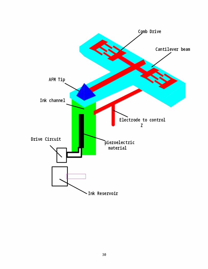
Figure 15. (a)The rise of a liquid column in a capillary tube; (b) the sink of a liquid column in a capillary tube.
30
Figure 16. Schematic representation of DP
31

Figure 17. Diagram showing water condensation and meniscus formation between a bare
tip sure face on the left, and a 1-dodecylamine modified tip and surface on the right.
Epson Stylus Color 850
1,440 x 720 1,440 x 720
8.26 x 43.34 (in.)
standard Micro Piezo no no
Epson Stylus Color 900
1,440 x 720 1,440 x 720
8.26 x 10.76 (in.)
standard micro piezo ink jet technology
yes no
32

Epson Stylus Photo 750
1,440 x 720 1,440 x 720
8.26 x 10.76 (in.)
standard micro piezo ink jet technology
yes no
HP DeskJet 697C
600 x 300 600 x 600
8 x 10.5 (in.)
yes (with special ink)
drop-on-demand thermal ink jet printing
yes no
HP DeskJet 712C
PhotoREt II 600 x 600
8 x 10.5 (in.)
standard drop-on-demand thermal ink jet
yes (PhotoREt II)
no
HP DeskJet 882C
photo quality with PhotoREt II
600 x 600 dpi
8 x 10.5 (in.)
yes (even on plain paper)
drop-on-demand thermal ink jet printing
yes (HP PhotoREt II)
no
HP DeskJet 895Cse
600 x 600 600 x 600
n/a yes drop-on-demand thermal ink jet
yes no
HP DeskJet 1120Cse
HP PhotoREt II
600 x 600
11 x 17 (in.)
standard thermal ink jet, HP PhotoREt II
yes yes
Lexmark 1100 Color Jetprinter
600 x 600 600 x 600
8.5 x 14 (in.)
no single-head ink jet
yes no
Lexmark 3200 Color Jetprinter
1,200 x 1,200
1,200 x 1,200
8.5 x 14 (in.)
yes (with special ink)
thermal ink jet yes no
Lexmark 5700 Color Jetprinter
1,200 x 1,200
1,200 x 1,200
8 x 16.8 (in.)
yes (with special ink)
Excimer Laser-Crafted Precision Inkjet
no no
Lexmark 5770 Photo Jetprinter
1,200 x 1,200
1,200 x 1,200
8.5 x 14 (in.)
yes Precision Ink jet, Laser-Crafted
no no
Lexmark Z51 Color Jetprinter
1,200 x 1,200
1,200 x 1,200
8 x 16.8 (in.)
standard 7 picoliter 1200 x 1200 dpi
yes yes
NEC SuperScript 650C
1,200 x 600 1,200 x 600
8.375 x 10.96 (in.)
yes (with special ink)
TrueColor plus Technology
no no
Okidata Okijet 2020
600 x 600 600 x 600
8.35 x 13 (in.)
no thermal ink jet no no
Okidata Okijet 2500
600 x 1,200 600 x 600
8.1 x 13.3 (in.)
yes (with special ink)
thermal ink jet yes no
Xerox DocuPrint XJ6C
1,200 x 600 600 x 600
18.29 x 13.5 (in.)
no thermal ink jet no no
Xerox DocuPrint XJ8C
1,200 x 1,200
1,200 x 1,200
8 x 16.8 (in.)
yes (with special ink)
thermal ink jet no no
1. Compare Different Company’s Ink-Jet printer
33
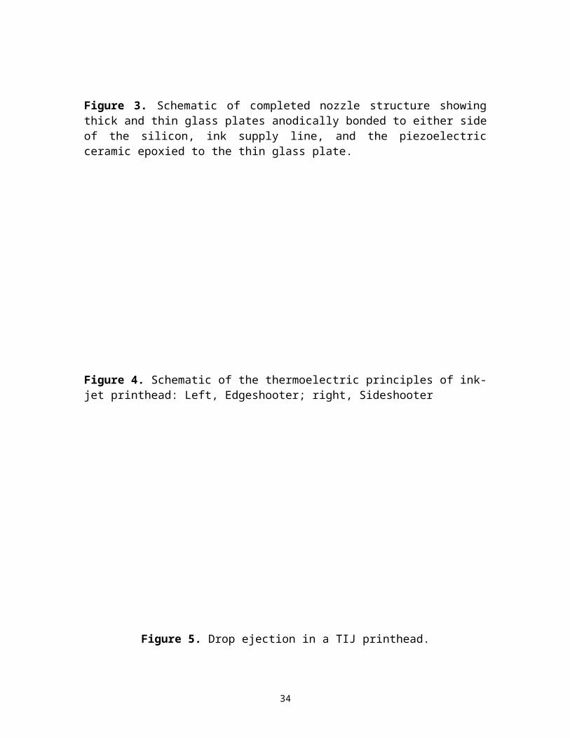
Table 2. Relevant properties of piezoelectric materials
34

Table 3. Magnitudes of surface tension and surface entropy for different liquids
35
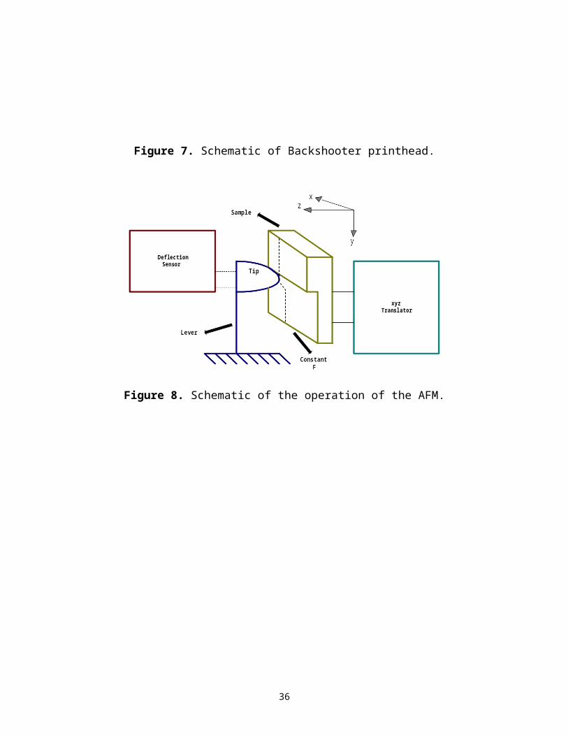
Table 4. Surface tension of selected solids and liquids
36
37


![Finale 2000c - [10-2467 Sanctus.MUS] - Hymnary.org](https://static.fdocuments.net/doc/165x107/61c9ddf1bef97f4dec5a12dd/finale-2000c-10-2467-hymnaryorg.jpg)