MCP3912 Data Sheet - Microchip Technologyww1.microchip.com/downloads/en/DeviceDoc/20005348A.pdf2014...
82
2014 Microchip Technology Inc. DS20005348A-page 1 MCP3912 Features: • Four Synchronous Sampling 24-bit Resolution Delta-Sigma A/D Converters • 93.5 dB SINAD, -107 dBc Total Harmonic Distortion (THD) (up to 35 th Harmonic), 112 dBFS SFDR for Each Channel • Enables 0.1% Typical Active Power Measurement Error over a 10,000:1 Dynamic Range • Advanced Security Features: - 16-Bit Cyclic Redundancy Check (CRC) Checksum on All Communications for Secure Data Transfers - 16-Bit CRC Checksum and Interrupt Alert for Register Map Configuration - Register Map lock with 8-Bit Secure Key • 2.7V-3.6V AV DD , DV DD • Programmable Data Rate up to 125 ksps: - 4 MHz Maximum Sampling Frequency - 16 MHz Maximum Master Clock • Oversampling Ratio up to 4096 • Ultra-Low Power Shutdown Mode with < 10 μA • -122 dB Crosstalk between Channels • Low-Drift 1.2V Internal Voltage Reference: 9 ppm/°C • Differential Voltage Reference Input Pins • High Gain PGA on Each Channel (up to 32 V/V) • Phase Delay Compensation with 1 μs Time Resolution • Separate Data Ready Pin for Easy Synchronization • Individual 24-Bit Digital Offset and Gain Error Correction for Each Channel • High-Speed 20 MHz SPI Interface with Mode 0,0 and 1,1 Compatibility • Continuous Read/Write Modes for Minimum Communication Time with Dedicated 16/32-Bit Modes • Available in 28-Lead QFN and 28-Lead SSOP Packages • Extended Temperature Range: -40°C to +125°C Description: The MCP3912 is a 3V four-channel Analog Front End (AFE) containing four synchronous sampling delta- sigma, Analog-to-Digital Converters (ADC), four PGAs, phase delay compensation block, low-drift internal voltage reference, digital offset and gain error calibration registers and high-speed 20 MHz SPI-compatible serial interface. The MCP3912 ADCs are fully configurable, with features such as 16/24-bit resolution, Oversampling Ratio (OSR) from 32 to 4096, gain from 1x to 32x, independent Shutdown and Reset, dithering and auto- zeroing. The communication is largely simplified with 8- bit commands, including various continuous read/write modes and 16/24/32-bit data formats that can be accessed by the Direct Memory Access (DMA) of an 8/16- or 32-bit MCU, and with the separate Data Ready pin that can directly be connected to an Interrupt Request (IRQ) input of an MCU. The MCP3912 includes advanced security features to secure the communications and the configuration settings, such as a CRC-16 checksum on both serial data outputs and static register map configuration. It also includes a register-map lock through an 8-bit secure key to stop unwanted write commands from processing. The MCP3912 is capable of interfacing with a variety of voltage and current sensors, including shunts, current transformers, Rogowski coils and Hall-effect sensors. Applications: • Polyphase Energy Meters • Energy Metering and Power Measurement • Automotive • Portable Instrumentation • Medical and Power Monitoring • Audio/Voice Recognition 3V Four-Channel Analog Front End
Transcript of MCP3912 Data Sheet - Microchip Technologyww1.microchip.com/downloads/en/DeviceDoc/20005348A.pdf2014...

MCP39123V Four-Channel Analog Front End
Features:• Four Synchronous Sampling 24-bit Resolution
Delta-Sigma A/D Converters
• 93.5 dB SINAD, -107 dBc Total Harmonic Distortion (THD) (up to 35th Harmonic), 112 dBFS SFDR for Each Channel
• Enables 0.1% Typical Active Power Measurement Error over a 10,000:1 Dynamic Range
• Advanced Security Features:
- 16-Bit Cyclic Redundancy Check (CRC) Checksum on All Communications for Secure Data Transfers
- 16-Bit CRC Checksum and Interrupt Alert for Register Map Configuration
- Register Map lock with 8-Bit Secure Key
• 2.7V-3.6V AVDD, DVDD
• Programmable Data Rate up to 125 ksps:
- 4 MHz Maximum Sampling Frequency
- 16 MHz Maximum Master Clock
• Oversampling Ratio up to 4096
• Ultra-Low Power Shutdown Mode with < 10 µA• -122 dB Crosstalk between Channels
• Low-Drift 1.2V Internal Voltage Reference: 9 ppm/°C
• Differential Voltage Reference Input Pins
• High Gain PGA on Each Channel (up to 32 V/V)
• Phase Delay Compensation with 1 µs Time Resolution
• Separate Data Ready Pin for Easy Synchronization
• Individual 24-Bit Digital Offset and Gain Error Correction for Each Channel
• High-Speed 20 MHz SPI Interface with Mode 0,0 and 1,1 Compatibility
• Continuous Read/Write Modes for Minimum Communication Time with Dedicated 16/32-Bit Modes
• Available in 28-Lead QFN and 28-Lead SSOP Packages
• Extended Temperature Range: -40°C to +125°C
Description:The MCP3912 is a 3V four-channel Analog Front End(AFE) containing four synchronous sampling delta-sigma, Analog-to-Digital Converters (ADC), four PGAs,phase delay compensation block, low-drift internalvoltage reference, digital offset and gain errorcalibration registers and high-speed 20 MHzSPI-compatible serial interface.
The MCP3912 ADCs are fully configurable, withfeatures such as 16/24-bit resolution, OversamplingRatio (OSR) from 32 to 4096, gain from 1x to 32x,independent Shutdown and Reset, dithering and auto-zeroing. The communication is largely simplified with 8-bit commands, including various continuous read/writemodes and 16/24/32-bit data formats that can beaccessed by the Direct Memory Access (DMA) of an8/16- or 32-bit MCU, and with the separate Data Readypin that can directly be connected to an InterruptRequest (IRQ) input of an MCU.
The MCP3912 includes advanced security features tosecure the communications and the configurationsettings, such as a CRC-16 checksum on both serialdata outputs and static register map configuration. Italso includes a register-map lock through an 8-bitsecure key to stop unwanted write commands fromprocessing.
The MCP3912 is capable of interfacing with a variety ofvoltage and current sensors, including shunts, currenttransformers, Rogowski coils and Hall-effect sensors.
Applications:
• Polyphase Energy Meters
• Energy Metering and Power Measurement
• Automotive
• Portable Instrumentation
• Medical and Power Monitoring
• Audio/Voice Recognition
2014 Microchip Technology Inc. DS20005348A-page 1
MCP3912
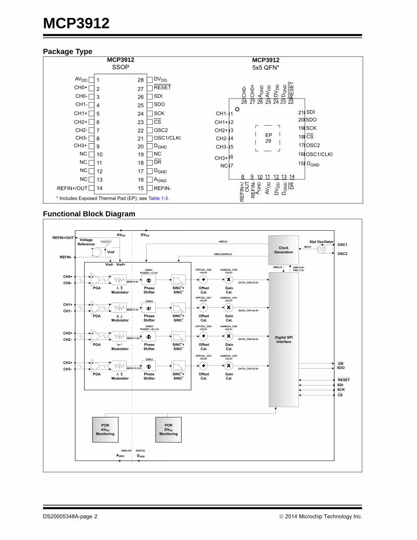
Package Type
Functional Block Diagram
2
26
3
4
5
6
10 11 12 13 14
18
17
16
15
28 27 25
CH
0+
CH
0-
CH1-
DV
DD
SDI
SDO
RE
SE
T
AG
ND
EP29
7
CH1+
CH2+ 19
20
24
SCK
23
CS
OSC2CH2-
22
OSC1/CLKI
1
8 9
NC
DG
ND
AV
DD
DGND
21
AG
ND
RE
FIN
-
DG
ND
AV
DD
DV
DD
CH3-
CH3+
MCP39125x5 QFN*
* Includes Exposed Thermal Pad (EP); see Table 1-3. RE
FIN
+/
1
2
3
4
5
6
7
8
9
10
11
12
13
14
28
27
26
25
24
23
22
21
20
19
18
17
16
15
AVDD
CH0+
CH0-
CH3+
NC
NC
NC
NC
REFIN+/OUT
CH1-
CH1+
CH2+
CH2-
CH3-
DVDD
RESET
SDI
DGND
NC
DR
DGND
AGND
REFIN-
SDO
SCK
CS
OSC2
OSC1/CLKI
MCP3912SSOP
OU
T
DR
AMCLK
DMCLK/DRCLK
REFIN+/OUT
REFIN-
PORAVDD
Monitoring
Vref+Vref-
VREFEXTVoltage
Reference
Vref+
-
Xtal OscillatorMCLK
OSC1
OSC2
Digital SPIInterface
Clock Generation
DMCLK OSR<2:0>PRE<1:0>
ANALOG DIGITAL
SDO
SDISCK
DR
RESET
CS
AGND DGND
AVDD DVDD
CH0+
CH0- -+
PGA
OSR/2-PHASE1 <11:0>
MOD<3:0>
Modulator
+
OFFCAL_CH0<23:0>
GAINCAL_CH0<23:0>
XDATA_CH0<23:0>
SINC3+SINC1
PhaseShifter
OffsetCal.
GainCal.
CH1+
CH1- -+
PGA
OSR/2
MOD<7:4>
Modulator
+
OFFCAL_CH1<23:0>
GAINCAL_CH1<23:0>
XDATA_CH1<23:0>
SINC3+SINC1
PhaseShifter
OffsetCal.
GainCal.
CH2+
CH2- -+
PGA
OSR/2-PHASE1 <23:12>
MOD<11:8>
Modulator
OFFCAL_CH2<23:0>
GAINCAL_CH2<23:0>
XDATA_CH2<23:0>
SINC3+SINC1
PhaseShifter
OffsetCal.
GainCal.
CH3+
CH3- -+
PGA
OSR/2
MOD<15:12>
Modulator
OFFCAL_CH3<23:0>
GAINCAL_CH3<23:0>
XDATA_CH3<23:0>
SINC3+SINC1
PhaseShifter
OffsetCal.
GainCal.
PORDVDD
Monitoring
DS20005348A-page 2 2014 Microchip Technology Inc.

MCP3912
1.0 ELECTRICAL CHARACTERISTICS
Absolute Maximum Ratings †
VDD ..................................................................... -0.3V to 4.0VDigital inputs and outputs w.r.t. AGND................. -0.3V to 4.0VAnalog input w.r.t. AGND..................................... ....-2V to +2VVREF input w.r.t. AGND ............................... -0.6V to VDD +0.6VStorage temperature .....................................-65°C to +150°CAmbient temp. with power applied ................-65°C to +125°CSoldering temperature of leads (10 seconds) ............. +300°CESD on all pins (HBM,MM) ....................................4 kV, 300V
† Notice: Stresses above those listed under “AbsoluteMaximum Ratings” may cause permanent damage tothe device. This is a stress rating only and functionaloperation of the device at those or any other condi-tions, above those indicated in the operational listingsof this specification, is not implied. Exposure to maxi-mum rating conditions for extended periods may affectdevice reliability.
1.1 Electrical Specifications
TABLE 1-1: ANALOG SPECIFICATIONSElectrical Specifications: Unless otherwise indicated, all parameters apply at AVDD = DVDD = 3V, MCLK = 4 MHz; PRE<1:0> = 00; OSR = 256; GAIN = 1; VREFEXT = 0, CLKEXT = 1, DITHER<1:0> = 11; BOOST<1:0> = 10, VCM = 0V; TA = -40°C to +125°C; VIN = -0.5 dBFS @ 50/60 Hz on all channels.
Characteristic Sym. Min. Typ. Max. Units Conditions
ADC Performance
Resolution (No missing codes)
24 — — bits OSR = 256 or greater
Sampling Frequency fS(DMCLK) — 1 4 MHz For maximum condition, BOOST<1:0> = 11
Output Data Rate fD(DRCLK) — 4 125 ksps For maximum condition, BOOST<1:0> = 11, OSR = 32
Analog Input Absolute Voltage on CHn+/- pins, n between 0 and 3
CHn+/- -1 — +1 V All analog input channels, measured to AGND
Analog Input Leakage Current
IIN — +/-1 — nA RESET<3:0> = 1111, MCLK running continuously
Differential Input Voltage Range
(CHn+-CHn-) -600/GAIN — +600/GAIN mV VREF = 1.2V, proportional to VREF
Offset Error VOS -1 0.2 1 mV Note 5
Offset Error Drift — 0.5 — µV/°C
Gain Error GE -5 — +5 % Note 5
Gain Error Drift — 1 — ppm/°C
Note 1: Dynamic Performance specified at -0.5 dB below the maximum differential input value, VIN = 1.2 VPP = 424 mVRMS @ 50/60 Hz, VREF = 1.2V. See Section 4.0 “Terminology And Formulas” for definition. This parameter is established by characterization and not 100% tested.
2: For these operating currents, the following configuration bit settings apply: SHUTDOWN<3:0> = 0000, RESET<3:0> = 0000, VREFEXT = 0, CLKEXT = 0.
3: For these operating currents, the following configuration bit settings apply: SHUTDOWN<3:0> = 1111, VREFEXT = 1, CLKEXT = 1.
4: Measured on one channel versus all others channels. The average of crosstalk performance over all channels (see Figure 2-32 for individual channel performance).
5: Applies to all gains. Offset and gain errors depend on PGA gain setting, see typical performance curves for typical performance.
6: Outside of this range, ADC accuracy is not specified. An extended input range of +/-2V can be applied continuously to the part with no damage.
7: For proper operation and for optimizing ADC accuracy, AMCLK should be limited to the maximum frequency defined in Table 5-2, as a function of the BOOST and PGA setting chosen. MCLK can take larger values as long as the prescaler settings (PRE<1:0>) limit AMCLK = MCLK/PRESCALE in the defined range in Table 5-2.
8: This parameter is established by characterization and not 100% tested.
2014 Microchip Technology Inc. DS20005348A-page 3

MCP3912
Integral Nonlinearity INL — 5 — ppm
Measurement Error ME — 0.1 — % Measured with a 10,000:1 dynamic range (from 600 mVPeak to 60 µVPeak), AVDD = DVDD = 3V, measurement points averaging time: 20 seconds, measured on each channel pair (CH0/1, CH2/3)
Differential Input Impedance
ZIN 232 — — k G = 1, proportional to 1/AMCLK
142 — — k G = 2, proportional to 1/AMCLK
72 — — k G = 4, proportional to 1/AMCLK
38 — — k G = 8, proportional to 1/AMCLK
36 — — k G = 16, proportional to 1/AMCLK
33 — — k G = 32, proportional to 1/AMCLK
Signal-to-Noise and Distortion Ratio (Note 1)
SINAD 92 93.5 — dB
Total Harmonic Distortion (Note 1)
THD — -107 -103 dBc Includes the first 35 harmonics
Signal-to-Noise Ratio (Note 1)
SNR 92 94 — dB
Spurious Free Dynamic Range (Note 1)
SFDR — 112 — dBFS
Crosstalk (50, 60 Hz) CTALK — -122 — dB Note 4
AC Power Supply Rejection
AC PSRR — -73 — dB AVDD = DVDD = 3V + 0.6VPP 50/60 Hz, 100/120 Hz
DC Power Supply Rejection
DC PSRR — -73 — dB AVDD = DVDD = 2.7V to 3.6V
DC Common Mode Rejection
DC CMRR — -100 — dB VCM from -1V to +1V
TABLE 1-1: ANALOG SPECIFICATIONS (CONTINUED)Electrical Specifications: Unless otherwise indicated, all parameters apply at AVDD = DVDD = 3V, MCLK = 4 MHz; PRE<1:0> = 00; OSR = 256; GAIN = 1; VREFEXT = 0, CLKEXT = 1, DITHER<1:0> = 11; BOOST<1:0> = 10, VCM = 0V; TA = -40°C to +125°C; VIN = -0.5 dBFS @ 50/60 Hz on all channels.
Characteristic Sym. Min. Typ. Max. Units Conditions
Note 1: Dynamic Performance specified at -0.5 dB below the maximum differential input value, VIN = 1.2 VPP = 424 mVRMS @ 50/60 Hz, VREF = 1.2V. See Section 4.0 “Terminology And Formulas” for definition. This parameter is established by characterization and not 100% tested.
2: For these operating currents, the following configuration bit settings apply: SHUTDOWN<3:0> = 0000, RESET<3:0> = 0000, VREFEXT = 0, CLKEXT = 0.
3: For these operating currents, the following configuration bit settings apply: SHUTDOWN<3:0> = 1111, VREFEXT = 1, CLKEXT = 1.
4: Measured on one channel versus all others channels. The average of crosstalk performance over all channels (see Figure 2-32 for individual channel performance).
5: Applies to all gains. Offset and gain errors depend on PGA gain setting, see typical performance curves for typical performance.
6: Outside of this range, ADC accuracy is not specified. An extended input range of +/-2V can be applied continuously to the part with no damage.
7: For proper operation and for optimizing ADC accuracy, AMCLK should be limited to the maximum frequency defined in Table 5-2, as a function of the BOOST and PGA setting chosen. MCLK can take larger values as long as the prescaler settings (PRE<1:0>) limit AMCLK = MCLK/PRESCALE in the defined range in Table 5-2.
8: This parameter is established by characterization and not 100% tested.
DS20005348A-page 4 2014 Microchip Technology Inc.

MCP3912
Internal Voltage Reference
Tolerance VREF 1.176 1.2 1.224 V VREFEXT = 0, TA = +25°C only
Temperature Coefficient TCVREF — 9 — ppm/°C TA = -40°C to +125°C, VREFEXT = 0, VREFCAL<7:0> = 0x50
Output Impedance ZOUTVREF — 0.6 — k VREFEXT = 0Internal Voltage Reference Operating Current
AIDDVREF — 54 — µA VREFEXT = 0, SHUTDOWN<3:0> = 1111
Voltage Reference Input
Input Capacitance — — 10 pF
Differential Input Voltage Range (VREF+ – VREF-)
VREF 1.1 — 1.3 V VREFEXT = 1
Absolute Voltage on REFIN+ pin
VREF+ VREF-+ 1.1
— VREF-+ 1.3
V VREFEXT = 1
Absolute Voltage REFIN- pin
VREF- -0.1 — +0.1 V REFIN- should be connected to AGND when VREFEXT = 0
Master Clock Input
Master Clock Input Frequency Range
fMCLK — — 20 MHz CLKEXT = 1, (Note 7)
Crystal Oscillator Operating Frequency Range
fXTAL 1 — 20 MHz CLKEXT = 0, (Note 7)
Analog Master Clock AMCLK — — 16 MHz (Note 7)
Crystal Oscillator Operating Current
DIDDXTAL — 80 — µA CLKEXT = 0
Power Supply
Operating Voltage, Analog AVDD 2.7 — 3.6 V
Operating Voltage, Digital DVDD 2.7 — 3.6 V
TABLE 1-1: ANALOG SPECIFICATIONS (CONTINUED)Electrical Specifications: Unless otherwise indicated, all parameters apply at AVDD = DVDD = 3V, MCLK = 4 MHz; PRE<1:0> = 00; OSR = 256; GAIN = 1; VREFEXT = 0, CLKEXT = 1, DITHER<1:0> = 11; BOOST<1:0> = 10, VCM = 0V; TA = -40°C to +125°C; VIN = -0.5 dBFS @ 50/60 Hz on all channels.
Characteristic Sym. Min. Typ. Max. Units Conditions
Note 1: Dynamic Performance specified at -0.5 dB below the maximum differential input value, VIN = 1.2 VPP = 424 mVRMS @ 50/60 Hz, VREF = 1.2V. See Section 4.0 “Terminology And Formulas” for definition. This parameter is established by characterization and not 100% tested.
2: For these operating currents, the following configuration bit settings apply: SHUTDOWN<3:0> = 0000, RESET<3:0> = 0000, VREFEXT = 0, CLKEXT = 0.
3: For these operating currents, the following configuration bit settings apply: SHUTDOWN<3:0> = 1111, VREFEXT = 1, CLKEXT = 1.
4: Measured on one channel versus all others channels. The average of crosstalk performance over all channels (see Figure 2-32 for individual channel performance).
5: Applies to all gains. Offset and gain errors depend on PGA gain setting, see typical performance curves for typical performance.
6: Outside of this range, ADC accuracy is not specified. An extended input range of +/-2V can be applied continuously to the part with no damage.
7: For proper operation and for optimizing ADC accuracy, AMCLK should be limited to the maximum frequency defined in Table 5-2, as a function of the BOOST and PGA setting chosen. MCLK can take larger values as long as the prescaler settings (PRE<1:0>) limit AMCLK = MCLK/PRESCALE in the defined range in Table 5-2.
8: This parameter is established by characterization and not 100% tested.
2014 Microchip Technology Inc. DS20005348A-page 5
MCP3912
1.2 Serial Interface Characteristics
Operating Current, Analog (Note 2)
IDD,A — 2.8 4 mA BOOST<1:0> = 00— 3.4 4.5 mA BOOST<1:0> = 01— 4.7 6.4 mA BOOST<1:0> = 10— 8.1 11.8 mA BOOST<1:0> = 11
Operating Current, Digital IDD,D — 0.28 0.6 mA MCLK = 4 MHz, proportional to MCLK (Note 2)
— 1.1 — mA MCLK = 16 MHz, proportional to MCLK (Note 2)
Shutdown Current, Analog IDDS,A — 0.01 2 µA AVDD pin only (Note 3) (Note 8)
Shutdown Current, Digital IDDS,D — 0.01 4 µA DVDD pin only (Note 3) (Note 8)
Pull-down Current on OSC2 Pin (External Clock mode only)
IOSC2 — 35 — µA CLKEXT = 1
TABLE 1-2: SERIAL DC CHARACTERISTICS
Electrical Specifications: Unless otherwise indicated, all parameters apply at DVDD = 2.7 to 3.6 V, TA = -40°C to +125°C, CLOAD = 30 pF, applies to all digital I/O.
Characteristic Sym. Min. Typ. Max. Units Conditions
High-Level Input Voltage VIH 0.7 DVDD — — V Schmitt-Triggered
Low-Level Input Voltage VIL — — 0.3 DVDD V Schmitt-Triggered
Input Leakage Current ILI — — ±1 µA CS = DVDD, VIN = DGND to DVDD
Output Leakage Current ILO — — ±1 µA CS = DVDD, VOUT = DGND or DVDD
Hysteresis Of Schmitt-Trigger Inputs
VHYS — 500 — mV DVDD = 3.3V only, Note 2
Low-Level Output Voltage VOL — — 0.2 DVDD V IOL = +1.7 mA
Note 1: This parameter is periodically sampled and not 100% tested.
2: This parameter is established by characterization and not production tested.
TABLE 1-1: ANALOG SPECIFICATIONS (CONTINUED)Electrical Specifications: Unless otherwise indicated, all parameters apply at AVDD = DVDD = 3V, MCLK = 4 MHz; PRE<1:0> = 00; OSR = 256; GAIN = 1; VREFEXT = 0, CLKEXT = 1, DITHER<1:0> = 11; BOOST<1:0> = 10, VCM = 0V; TA = -40°C to +125°C; VIN = -0.5 dBFS @ 50/60 Hz on all channels.
Characteristic Sym. Min. Typ. Max. Units Conditions
Note 1: Dynamic Performance specified at -0.5 dB below the maximum differential input value, VIN = 1.2 VPP = 424 mVRMS @ 50/60 Hz, VREF = 1.2V. See Section 4.0 “Terminology And Formulas” for definition. This parameter is established by characterization and not 100% tested.
2: For these operating currents, the following configuration bit settings apply: SHUTDOWN<3:0> = 0000, RESET<3:0> = 0000, VREFEXT = 0, CLKEXT = 0.
3: For these operating currents, the following configuration bit settings apply: SHUTDOWN<3:0> = 1111, VREFEXT = 1, CLKEXT = 1.
4: Measured on one channel versus all others channels. The average of crosstalk performance over all channels (see Figure 2-32 for individual channel performance).
5: Applies to all gains. Offset and gain errors depend on PGA gain setting, see typical performance curves for typical performance.
6: Outside of this range, ADC accuracy is not specified. An extended input range of +/-2V can be applied continuously to the part with no damage.
7: For proper operation and for optimizing ADC accuracy, AMCLK should be limited to the maximum frequency defined in Table 5-2, as a function of the BOOST and PGA setting chosen. MCLK can take larger values as long as the prescaler settings (PRE<1:0>) limit AMCLK = MCLK/PRESCALE in the defined range in Table 5-2.
8: This parameter is established by characterization and not 100% tested.
DS20005348A-page 6 2014 Microchip Technology Inc.
MCP3912
High-Level Output Voltage VOH 0.75 DVDD — — V IOH = -1.7 mA
Internal Capacitance(All Inputs And Outputs)
CINT — — 7 pF TA = +25°C, SCK = 1.0 MHz,DVDD =3.3V (Note 1)
TABLE 1-2: SERIAL DC CHARACTERISTICS (CONTINUED)
Electrical Specifications: Unless otherwise indicated, all parameters apply at DVDD = 2.7 to 3.6 V, TA = -40°C to +125°C, CLOAD = 30 pF, applies to all digital I/O.
Characteristic Sym. Min. Typ. Max. Units Conditions
Note 1: This parameter is periodically sampled and not 100% tested.
2: This parameter is established by characterization and not production tested.
2014 Microchip Technology Inc. DS20005348A-page 7

MCP3912
TABLE 1-3: SERIAL AC CHARACTERISTICS TABLE
Electrical Specifications: Unless otherwise indicated, all parameters apply at DVDD = 2.7 to 3.6 V, TA = -40°C to +125°C, GAIN = 1, CLOAD = 30 pF
Characteristic Sym. Min. Typ. Max. Units Conditions
Serial Clock Frequency fSCK — — 20 MHz
CS Setup Time tCSS 25 — — ns
CS Hold Time tCSH 50 — — ns
CS Disable Time tCSD 50 — — ns
Data Setup Time tSU 5 — — ns
Data Hold Time tHD 10 — — ns
Serial Clock High Time tHI 20 — — ns
Serial Clock Low Time tLO 20 — — ns
Serial Clock Delay Time tCLD 50 — — ns
Serial Clock Enable Time tCLE 50 — — ns
Output Valid from SCK Low tDO — — 25 ns
Output Hold Time tHO 0 — — ns Note 1
Output Disable Time tDIS — — 25 ns Note 1
Reset Pulse Width (RESET) tMCLR 100 — — ns
Data Transfer Time to DR (Data Ready)
tDODR — — 25 ns Note 2
Data Ready Pulse Low Time tDRP — 1/(2 x DMCLK) — µs
Note 1: This parameter is periodically sampled and not 100% tested.
2: This parameter is established by characterization and not production tested.
TABLE 1-4: TEMPERATURE SPECIFICATIONS TABLE
Electrical Specifications: Unless otherwise indicated, all parameters apply at AVDD = 2.7 to 3.6V, DVDD = 2.7 to 3.6V.
Parameters Sym. Min. Typ. Max. Units. Conditions
Temperature Ranges
Operating Temperature Range TA -40 — +125 °C Note 1
Storage Temperature Range TA -65 — +150 °C
Thermal Package Resistances
Thermal Resistance, 28L SSOP JA — 80 — °C/W
Thermal Resistance, 28L QFN JA — 41 — °C/W
Note 1: The internal junction temperature (TJ) must not exceed the absolute maximum specification of +150°C.
DS20005348A-page 8 2014 Microchip Technology Inc.
MCP3912
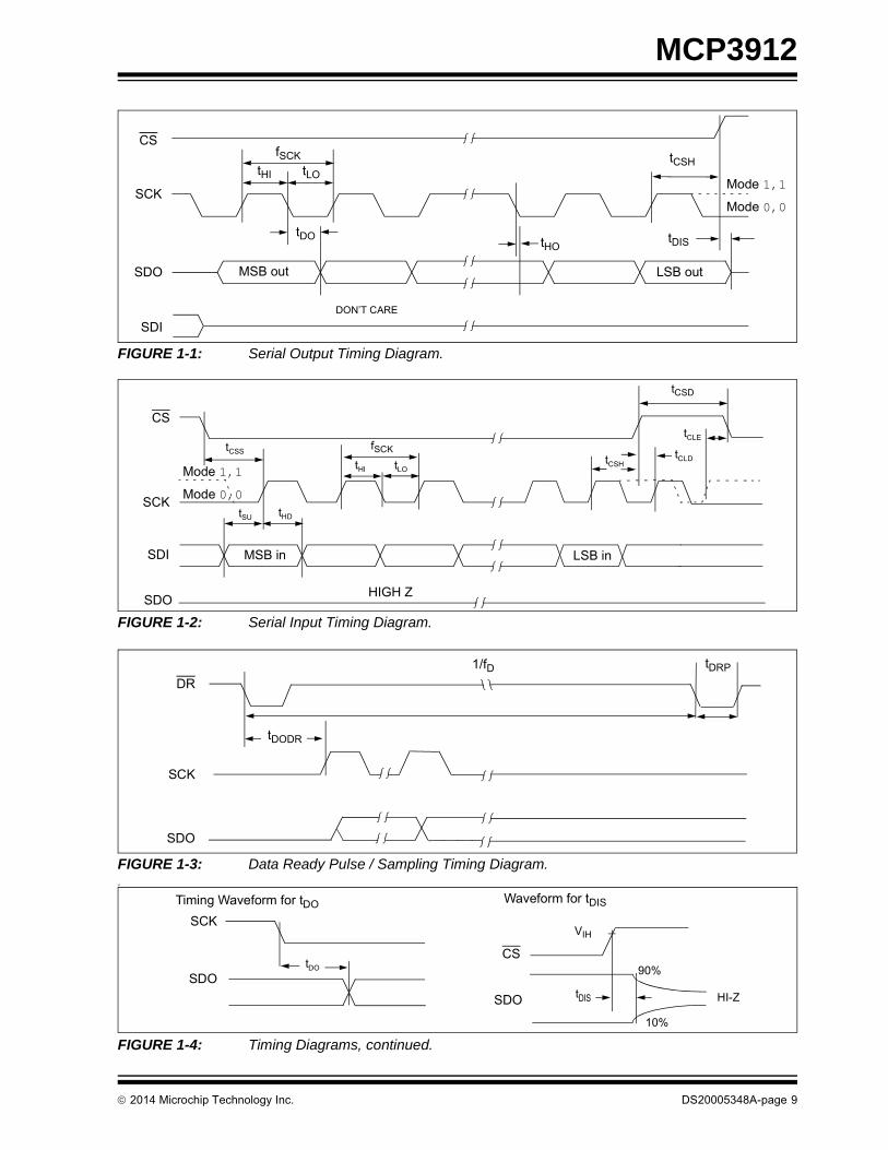
FIGURE 1-1: Serial Output Timing Diagram.
FIGURE 1-2: Serial Input Timing Diagram.
FIGURE 1-3: Data Ready Pulse / Sampling Timing Diagram.H
FIGURE 1-4: Timing Diagrams, continued.
tCSH
tDIS
tHI tLO
fSCK
CS
SCK
SDO MSB out LSB out
SDI
Mode 1,1Mode 0,0
tHOtDO
DON’T CARE
CS
SCK
SDI LSB inMSB in
Mode 1,1Mode 0,0
tCSS
tSU tHD
tCSD
tCSHtCLD
tCLE
SDOHIGH Z
tHI tLO
fSCK
DR
SCK
tDRP
SDO
1/fD
tDODR
CS
VIH
Waveform for tDIS
HI-Z
90%
10%
tDISSDO
SCK
SDOtDO
Timing Waveform for tDO
2014 Microchip Technology Inc. DS20005348A-page 9

MCP3912
2.0 TYPICAL PERFORMANCE CURVES
Note: Unless otherwise indicated, AVDD = 3V, DVDD = 3V; TA = +25°C, MCLK = 4 MHz; PRESCALE = 1; OSR = 256; GAIN = 1; Dithering = Maximum; VIN = -0.5 dBFS @ 60 Hz on all channels, VREFEXT = 0; CLKEXT = 1;BOOST<1:0> = 10.
FIGURE 2-1: Spectral Response.
FIGURE 2-2: Spectral Response.
FIGURE 2-3: Spectral Response.
FIGURE 2-4: Spectral Response.
FIGURE 2-5: Measurement Error with 1-Point Calibration.
FIGURE 2-6: Measurement Error with 2-Point Calibration.
Note: The graphs and tables provided following this note are a statistical summary based on a limited number ofsamples and are provided for informational purposes only. The performance characteristics listed hereinare not tested or guaranteed. In some graphs or tables, the data presented may be outside the specifiedoperating range (e.g., outside specified power supply range) and therefore outside the warranted range.
-140-120-100-80-60-40-20
0
Am
plitu
de (d
B)
Vin = -0.5 dBFS @ 60 HzfD = 3.9 kspsOSR = 256Dithering = Off16 ksamples FFT
-180-160140
0 500 1000 1500 2000Frequency (Hz)
200
Vin = -60 dBFS @ 60 Hz
-40-20
B)
fD = 3.9 kspsOSR = 256Dithering = Off
-80-60
de (d
B 16 ksamples FFT
-120-100
mpl
itu
-160-140
A
-180-160
0 500 1000 1500 20000 500 1000 1500 2000Frequency (Hz)
-140-120-100-80-60-40-20
0
Am
plitu
de (d
B)
Vin = -0.5 dBFS @ 60 HzfD = 3.9 kspsOSR = 256Dithering = Maximum16 ksamples FFT
-180-160140
0 500 1000 1500 2000Frequency (Hz)
0
-40-20
0
)
Vin = -60 dBFS @ 60 HzfD = 3.9 kspsOSR = 256
-80-60
de (d
B)
Dithering = Maximum16 ksamples FFT
-120-100
mpl
itud
-160-140A
m
-1800 500 1000 1500 2000
Frequency (Hz)
-1.0%
-0.5%
0.0%
0.5%
1.0%
0.01 0.1 1 10 100 1000
Mea
sure
men
t Err
or (%
)
Current Channel Input Amplitude (mVPeak)
% Error Channel 0, 1
-1.0%
-0.5%
0.0%
0.5%
1.0%
0.01 0.1 1 10 100 1000
Mea
sure
men
t Err
or (%
)
Current Channel Input Amplitude (mVPeak)
% Error Channel 0, 1
DS20005348A-page 10 2014 Microchip Technology Inc.

MCP3912
Note: Unless otherwise indicated, AVDD = 3V, DVDD = 3V; TA = +25°C, MCLK = 4 MHz; PRESCALE = 1; OSR = 256; GAIN = 1; Dithering = Maximum; VIN = -0.5 dBFS @ 60 Hz on all channels, VREFEXT = 0; CLKEXT = 1;BOOST<1:0> = 10.
FIGURE 2-7: THD Repeatability Histogram.
FIGURE 2-8: Spurious Free Dynamic Range Repeatability Histogram.
FIGURE 2-9: SINAD Repeatability Histogram.
FIGURE 2-10: Output Noise Histogram.
FIGURE 2-11: THD vs.OSR.
FIGURE 2-12: SINAD vs. OSR.
err
ence
f Occ
uen
cy o
fFr
eque
-108.2 -107.8 -107.4 -107.0 -106.6 -106.2
F
Total Harmonic Distortion ( dBc)Total Harmonic Distortion (-dBc)
quen
cy o
f Occ
urre
nce
111.7 112.3 112.9 113.5 114.1 114.7 115.3 115.9
Freq
Spurious Free Dynamic Range (dBFS)
eur
renc
eof
Occ
uen
cyo
Freq
u
93.3 93.4 93.5 93.6 93.7 93.8Signal to Noise and Distortion (dB)Signal to Noise and Distortion (dB)
uenc
y of
Occ
urre
nce Standar deviation = 78 LSB
Noise = 7.4 Vrms16 ksamples
448
481
514
548
581
614
647
680
714
747
780
813
846
880
913
946
979
1,01
21,
046
1,07
91,
112
Freq
u
Output Noise (LSB)
-120-115-110-105-100-95-90
al H
arm
onic
Dis
tort
ion
(dB
c)
Dithering=MaximumDithering=MediumDithering=MinimumDithering=Off
-130-125
32 64 128 256 512 1024 2048 4096
Tot
Oversampling Ratio (OSR)
110
95100105
nd dB)
859095
Noi
se a
Rat
io (d
758085
al-to
-Nor
tion
R
Dithering=Maximu
6570
Sign
Dis
to
Dithering MaximumDithering=Medium
6032 64 128 256 512 1024 2048 4096
Oversampling Ratio (OSR)Oversampling Ratio (OSR)
2014 Microchip Technology Inc. DS20005348A-page 11

MCP3912
Note: Unless otherwise indicated, AVDD = 3V, DVDD = 3V; TA = +25°C, MCLK = 4 MHz; PRESCALE = 1; OSR = 256; GAIN = 1; Dithering = Maximum; VIN = -0.5 dBFS @ 60 Hz on all channels, VREFEXT = 0; CLKEXT = 1;BOOST<1:0> = 10.L
FIGURE 2-13: SNR vs.OSR.
FIGURE 2-14: SFDR vs. OSR.
FIGURE 2-15: THD vs. MCLK.
FIGURE 2-16: SINAD vs. MCLK.
FIGURE 2-17: SNR vs. MCLK.
FIGURE 2-18: SFDR vs. MCLK.
110
95100105
(dB
)
859095
Rat
io(
758085
-Noi
se
Dithering=Maximum
657075
nal-t
o-
Dithering MaximumDithering=MediumDithering=MinimumDithering=Off
6032 64 128 256 512 1024 2048 4096
Sig
O li R ti (OSR)Oversampling Ratio (OSR)
120
110115
nam
ic)
100105110
ee D
yn(d
BFS
)
95100
ous
Fre
Ran
ge(
Dithering=Maximum
8590
Spur
io R gDithering=MediumDithering=MinimumDithering=Off
8032 64 128 256 512 1024 2048 4096
O li R ti (OSR)
Dithering Off
Oversampling Ratio (OSR)
100-95-90-85-80-75-70-65-60
al H
arm
onic
Dis
tort
ion
(dB
)
Boost = 00Boost = 01Boost = 10Boost = 11
-110-105-100
2 4 6 8 10 12 14 16 18 20
Tota
MCLK Frequency (MHz)
100
90
95
e an
d
80
85
o-N
oise
tort
ion
dB)
75
80
gnal
-to Dis
t (
65
70Sig
Boost = 00Boost = 01
602 4 6 8 10 12 14 16 18
Boost = 10
MCLK Frequency (MHz)
100
90
95
tio
80
85is
e R
at)
75
80
-to-N
o(d
B)
65
70
Sign
al
Boost = 00Boost = 01Boost = 10
602 4 6 8 10 12 14 16 18
Boost = 10Boost = 11
MCLK Frequency (MHz)
120
110
amic
90
100
ee D
ynge FS
)
80
90
ous
Fre
Ran
(dB
F
70
80
Spur
io Boost = 00Boost = 01Boost = 10
602 4 6 8 10 12 14 16 18 20
Boost = 11
2 4 6 8 10 12 14 16 18 20MCLK Frequency (MHz)
DS20005348A-page 12 2014 Microchip Technology Inc.
MCP3912
Note: Unless otherwise indicated, AVDD = 3V, DVDD = 3V; TA = +25°C, MCLK = 4 MHz; PRESCALE = 1; OSR = 256; GAIN = 1; Dithering = Maximum; VIN = -0.5 dBFS @ 60 Hz on all channels, VREFEXT = 0; CLKEXT = 1;BOOST<1:0> = 10.
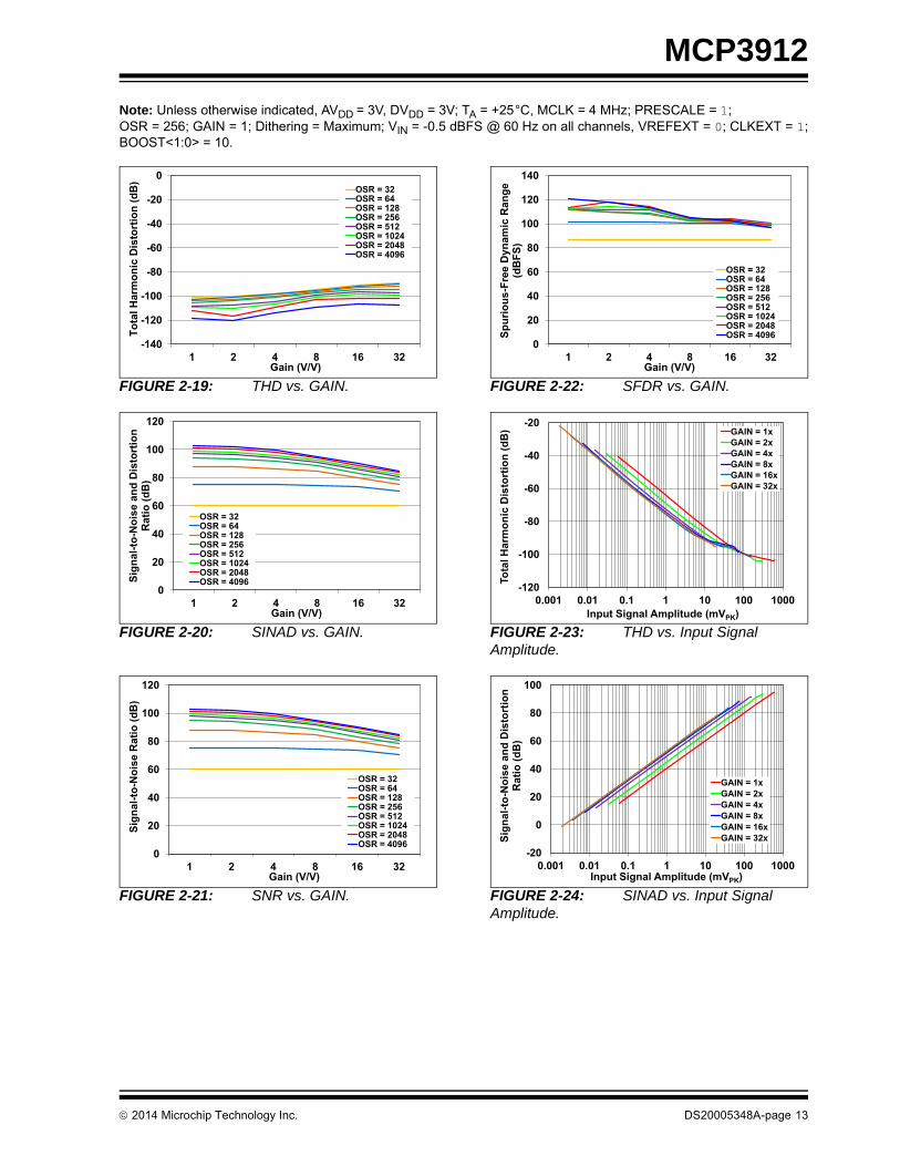
FIGURE 2-19: THD vs. GAIN.
FIGURE 2-20: SINAD vs. GAIN.
FIGURE 2-21: SNR vs. GAIN.
FIGURE 2-22: SFDR vs. GAIN.
FIGURE 2-23: THD vs. Input Signal Amplitude.
FIGURE 2-24: SINAD vs. Input Signal Amplitude.
-140
-120
-100
-80
-60
-40
-20
0
1 2 4 8 16 32
Tota
l Har
mon
icD
isto
rio
n(d
B)
Gain (V/V)
OSR = 32OSR = 64OSR = 128OSR = 256OSR = 512OSR = 1024OSR = 2048OSR = 4096
0
20
40
60
80
100
120
1 2 4 8 16 32
Sign
al-to
-Noi
se a
nd D
isto
rtio
n R
atio
(dB
)
Gain (V/V)
OSR = 32OSR = 64OSR = 128OSR = 256OSR = 512OSR = 1024OSR = 2048OSR = 4096
0
20
40
60
80
100
120
1 2 4 8 16 32
Sign
al-to
-Noi
se R
atio
(dB
)
Gain (V/V)
OSR = 32OSR = 64OSR = 128OSR = 256OSR = 512OSR = 1024OSR = 2048OSR = 4096
0
20
40
60
80
100
120
140
1 2 4 8 16 32
Spur
ious
Free
Dyn
amic
Ran
ge(d
BFS
)
Gain (V/V)
OSR = 32OSR = 64OSR = 128OSR = 256OSR = 512OSR = 1024OSR = 2048OSR = 4096
-120
-100
-80
-60
-40
-20
0.001 0.01 0.1 1 10 100 1000
Tota
l Har
mon
ic D
isto
rtio
n (d
B)
Input Signal Amplitude (mVPK)
GAIN = 1xGAIN = 2xGAIN = 4xGAIN = 8xGAIN = 16xGAIN = 32x
-20
0
20
40
60
80
100
0.001 0.01 0.1 1 10 100 1000
Sign
al-to
-Noi
se a
nd D
isto
rtio
n R
atio
(dB
)
Input Signal Amplitude (mVPK)
GAIN = 1xGAIN = 2xGAIN = 4xGAIN = 8xGAIN = 16xGAIN = 32x
2014 Microchip Technology Inc. DS20005348A-page 13
MCP3912
Note: Unless otherwise indicated, AVDD = 3V, DVDD = 3V; TA = +25°C, MCLK = 4 MHz; PRESCALE = 1; OSR = 256; GAIN = 1; Dithering = Maximum; VIN = -0.5 dBFS @ 60 Hz on all channels, VREFEXT = 0; CLKEXT = 1;BOOST<1:0> = 10.
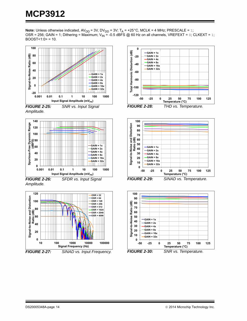
FIGURE 2-25: SNR vs. Input Signal Amplitude.
FIGURE 2-26: SFDR vs. Input Signal Amplitude.
FIGURE 2-27: SINAD vs. Input Frequency.
FIGURE 2-28: THD vs. Temperature.
FIGURE 2-29: SINAD vs. Temperature.
FIGURE 2-30: SNR vs. Temperature.
-20
0
20
40
60
80
100
0.001 0.01 0.1 1 10 100 1000
Sign
al-to
-Noi
se R
atio
(dB
)
Input Signal Amplitude (mVPK)
GAIN = 1xGAIN = 2xGAIN = 4xGAIN = 8xGAIN = 16xGAIN = 32x
0
20
40
60
80
100
120
140
0.001 0.01 0.1 1 10 100 1000
Spur
ious
Free
Dya
nmic
Ran
ge(d
BFS
)
Input Signal Amplitude (mVPK)
GAIN = 1xGAIN = 2xGAIN = 4xGAIN = 8xGAIN = 16xGAIN = 32x
0
20
40
60
80
100
120
10 100 1000 10000 100000
Sign
al-to
-Noi
se a
nd D
isto
rtio
n R
atio
(dB
)
Signal Frequency (Hz)
OSR = 32OSR = 64OSR = 128OSR = 256OSR = 512OSR = 1024OSR = 2048OSR = 4096
-120
-100
-80
-60
-40
-20
0
-50 -25 0 25 50 75 100 125
Tota
l Har
mon
ic D
isto
rtio
n(d
B)
Temperature (°C)
GAIN = 1xGAIN = 2xGAIN = 4xGAIN = 8xGAIN = 16xGAIN = 32x
0 102030405060708090
100
-50 -25 0 25 50 75 100 125
Sign
al-to
-Noi
se a
ndD
isto
rtio
nR
atio
(dB
)
Temperature (°C)
GAIN = 1xGAIN = 2xGAIN = 4xGAIN = 8xGAIN = 16xGAIN = 32x
0102030405060708090
100
-50 -25 0 25 50 75 100 125
Sign
al-to
-Noi
se R
atio
(dB
)
Temperature (°C)
GAIN = 1xGAIN = 2xGAIN = 4xGAIN = 8xGAIN = 16xGAIN = 32x
DS20005348A-page 14 2014 Microchip Technology Inc.

MCP3912
Note: Unless otherwise indicated, AVDD = 3V, DVDD = 3V; TA = +25°C, MCLK = 4 MHz; PRESCALE = 1; OSR = 256; GAIN = 1; Dithering = Maximum; VIN = -0.5 dBFS @ 60 Hz on all channels, VREFEXT = 0; CLKEXT = 1;BOOST<1:0> = 10.
FIGURE 2-31: SFDR vs. Temperature.
FIGURE 2-32: Crosstalk vs. Measured Channel.
FIGURE 2-33: Offset vs. Temperature vs. Gain.
FIGURE 2-34: Channel Offset Matching vs. Temperature.
FIGURE 2-35: Gain Error vs. Temperature vs. Gain.
FIGURE 2-36: Internal Voltage Reference vs. Temperature.
0
20
40
60
80
100
120
-50 -25 0 25 50 75 100 125
Spur
ious
Free
Dya
nmic
Ran
ge(d
BFS
)
Temperature (°C)
GAIN = 1xGAIN = 2xGAIN = 4xGAIN = 8xGAIN = 16xGAIN = 32x
-140
-120
-100
-80
-60
-40
-20
0
0 1 2 3
Cro
ssta
lk (d
B)
Measured Channel*
28LD SSOP
28LD QFN
* All other channels at maximum amplitude VIN = 600 mVPK @ 60 Hz
-1000-800-600-400-200
0200400600800
1000
-40 -20 0 20 40 60 80 100 120
Offs
et (µ
V)
Temperature (°C)
GAIN = 1xGAIN = 2xGAIN = 4xGAIN = 8xGAIN = 16xGAIN = 32x
-1000-800-600-400-200
0200400600800
1000
-40 -20 0 20 40 60 80 100 120
Cha
nnel
Offs
et (µ
V)
Temperature (°C)
Channel 0
Channel 1
Channel 2
Channel 3
-5
-3
-1
1
3
5
7
9
-40 -20 0 20 40 60 80 100 120
Gai
n Er
ror (
%)
Temperature (°C)
GAIN = 1xGAIN = 2xGAIN = 4xGAIN = 8xGAIN = 16xGAIN = 32x
1.197
1.198
1.199
1.2
-40 -20 0 20 40 60 80 100 120 140
Inte
rnal
Vol
tage
Ref
eren
ce (V
)
Temperature (°C)
2014 Microchip Technology Inc. DS20005348A-page 15

MCP3912
Note: Unless otherwise indicated, AVDD = 3V, DVDD = 3V; TA = +25°C, MCLK = 4 MHz; PRESCALE = 1; OSR = 256; GAIN = 1; Dithering = Maximum; VIN = -0.5 dBFS @ 60 Hz on all channels, VREFEXT = 0; CLKEXT = 1;BOOST<1:0> = 10.
FIGURE 2-37: Internal Voltage Reference vs. Supply Voltage.
FIGURE 2-38: Integral Nonlinearity (Dithering Maximum).
FIGURE 2-39: Integral Nonlinearity (Dithering Off).
FIGURE 2-40: Operating Current vs. MCLK Frequency vs. Boost, VDD = 3V.
1.1961
1.1962
1.1963
1.1964
1.1965
1.1966
1.1967
1.1968
1.1969
2.5 2.6 2.7 2.8 2.9 3 3.1 3.2 3.3 3.4 3.5 3.6
Inte
rnal
Vol
tage
Ref
eren
ce (V
)
AVDD (V)
-10-8 -6 -4 -2 0 2 4 6 8
10
-0.6 -0.4 -0.2 0.0 0.2 0.4 0.6
Inte
gral
Non
Line
arity
Erro
r(p
pm)
Input Voltage (V)
-10-8 -6 -4 -2 0 2 4 6 8
10
-0.6 -0.4 -0.2 0.0 0.2 0.4 0.6
Inte
gral
Non
Line
arity
Erro
r(p
pm)
Input Voltage (V)
0
2
4
6
8
10
12
14
2 4 6 8 10 12 14 16 18 20 22 24 26 28
I DD (m
A)
MCLK (MHz)
AIDD Boost =0.5xAIDD Boost =0.66xAIDD Boost =1xAIDD Boost =2xDIDD
DS20005348A-page 16 2014 Microchip Technology Inc.
MCP3912
NOTES:
2014 Microchip Technology Inc. DS20005348A-page 17

MCP3912
3.0 PIN DESCRIPTION
Descriptions of the pins are listed in Table 3-1.
TABLE 3-1: FOUR CHANNEL MCP3912 PIN FUNCTION TABLE
MCP3912SSOP
MCP3912QFN
Symbol Function
1 25, 11 AVDD Analog Power Supply Pin
2 27 CH0+ Noninverting Analog Input Pin for Channel 0
3 28 CH0- Inverting Analog Input Pin for Channel 0
4 29 CH1- Inverting Analog Input Pin for Channel 1
5 2 CH1+ Noninverting Analog Input Pin for Channel 1
6 3 CH2+ Noninverting Analog Input Pin for Channel 2
7 4 CH2- Inverting Analog Input Pin for Channel 2
8 5 CH3- Inverting Analog Input Pin for Channel 3
9 6 CH3+ Noninverting Analog Input Pin for Channel 3
10, 11, 12, 13, 19
7 NC No Connect (for better EMI results connect to AGND)
14 8 REFIN+/OUT Noninverting Voltage Reference Input and Internal Reference Output Pin
15 9 REFIN- Inverting Voltage Reference Input Pin
16 10, 26 AGND Analog Ground Pin, Return Path for Internal Analog Circuitry
17, 20 13, 15, 23 DGND Digital Ground Pin, Return Path for Internal Digital Circuitry
18 14 DR Data Ready Signal Output Pin
21 16 OSC1/CLKI Oscillator Crystal Connection Pin or External Clock Input Pin
22 17 OSC2 Oscillator Crystal Connection Pin
23 18 CS Serial Interface Chip Select Input Pin
24 19 SCK Serial Interface Clock Input Pin for SPI
25 20 SDO Serial Interface Data Output Pin
26 21 SDI Serial Interface Data Input Pin
27 22 RESET Master Reset Logic Input Pin
28 12, 14 DVDD Digital Power Supply Pin
— 29 EP Exposed Thermal Pad. Must be connected to AGND or floating.
DS20005348A-page 18 2014 Microchip Technology Inc.

MCP3912
3.1 Analog Power Supply (AVDD)
AVDD is the power supply voltage for the analogcircuitry within the MCP3912. It is distributed on severalpins (pins 11 and 25 in the QFN-28 package, one pinonly in the SSOP-28 package). For optimalperformance, connect these pins together using a starconnection, and connect the appropriate bypasscapacitors (typically a 10 µF in parallel with a 0.1 µFceramic). AVDD should be maintained between 2.7Vand 3.6V for specified operation.
To ensure proper functionality of the device, at leastone of these pins must be properly connected. Toensure optimal performance of the device, all the pinsmust be properly connected. If any of these pins are leftfloating, the accuracy and noise specifications are notensured.
3.2 ADC Differential Analog Inputs (CHn+/CHn-)
The CHn+/- pins (n comprised between 0 and 3) arethe four fully-differential analog voltage inputs for thedelta-sigma ADCs.
The linear and specified region of the channels isdependent on the PGA gain. This region correspondsto a differential voltage range of ±600 mV/GAIN withVREF = 1.2V.
The maximum absolute voltage, with respect to AGND,for each CHn+/- input pin is ±1V with no distortion, and±2V with no breaking after continuous voltage. Thismaximum absolute voltage is not proportional to theVREF voltage.
3.3 Noninverting Reference Input, Internal Reference Output (REFIN+/OUT)
This pin is the noninverting side of the differentialvoltage reference input for all ADCs or the internalvoltage reference output.
When VREFEXT = 1, an external voltage referencesource can be used, and the internal voltage referenceis disabled. When using an external differential voltagereference, it should be connected to its VREF+ pin.When using an external single-ended reference, itshould be connected to this pin.
When VREFEXT = 0, the internal voltage reference isenabled and connected to this pin through a switch.This voltage reference has minimal drive capability andthus needs proper buffering and bypass capacitances(a 0.1 µF ceramic capacitor is sufficient in most cases)if used as a voltage source.
If the voltage reference is only used as an internalVREF, adding bypass capacitance on REFIN+/OUT isnot necessary for keeping ADC accuracy, but a minimal0.1 µF ceramic capacitance can be connected to avoidEMI/EMC susceptibility issues due to the antennacreated by the REFIN+/OUT pin if left floating.
3.4 Inverting Reference Input (REFIN-)
This pin is the inverting side of the differential voltagereference input for all ADCs. When using an externaldifferential voltage reference, it should be connected toits VREF- pin. When using an external single-endedvoltage reference, or when VREFEXT = 0 (default) andusing the internal voltage reference, the pin should bedirectly connected to AGND.
3.5 Analog Ground (AGND)
AGND is the ground reference voltage for the analogcircuitry within the MCP3912. It is distributed on severalpins (pins 10 and 26 in the QFN-28 package, one pinonly in the SSOP-28 package). For optimalperformance, it is recommended to connect these pinstogether using a star connection, and to connect it tothe same ground node voltage as DGND with a starconnection.
At least one of these pins needs to be properlyconnected to ensure proper functionality of the device.All of these pins need to be properly connected toensure optimal performance of the device. If any ofthese pins are left floating, the accuracy and noisespecifications are not ensured. If an analog groundplane is available, it is recommended that these pins betied to this plane of the PCB. This plane should alsoreference all other analog circuitry in the system.
3.6 Digital Ground (DGND)
DGND is the ground reference voltage for the digitalcircuitry within the MCP3912. It is distributed on severalpins (pins 13, 15 and 23 in the QFN-28 package, twopins only in the SSOP-28 package). For optimalperformance, connect these pins together using a starconnection and connect it to the same ground nodevoltage as AGND with a star connection.
At least one of these pins needs to be properlyconnected to ensure proper functionality of the device.All of these pins need to be properly connected toensure optimal performance of the device. If any ofthese pins are left floating, the accuracy and noisespecifications are not ensured. If a digital ground planeis available, it is recommended that these pins be tiedto this plane of the Printed Circuit Board (PCB). Thisplane should also reference all other digital circuitry inthe system.
2014 Microchip Technology Inc. DS20005348A-page 19

MCP3912
3.7 Data Ready Output (DR)
The Data Ready pin indicates if a new conversionresult is ready to be read. The default state of this pinis logic high when DR_HIZ = 1, and is high-impedancewhen DR_HIZ = 0 (default). After each conversion isfinished, a logic low pulse will take place on the dataready pin to indicate the conversion result is ready asan interrupt. This pulse is synchronous with the masterclock and has a defined and constant width.
The Data Ready pin is independent of the SPI interfaceand acts like an interrupt output. The Data Ready pinstate is not latched, and the pulse width (and period)are both determined by the MCLK frequency,over-sampling rate and internal clock prescale settings.The data ready pulse width is equal to half a DMCLKperiod, and the frequency of the pulses is equal toDRCLK (see Figure 1-3).
3.8 Oscillator and Master Clock Input Pin (OSC1/CLKI)
OSC1/CLKI and OSC2 provide the master clock for thedevice. When CLKEXT = 0, a resonant crystal or clocksource with a similar sinusoidal waveform must beplaced across the OSC1 and OSC2 pins to ensureproper operation.
The typical clock frequency specified is 4 MHz. Forproper operation and for optimizing ADC accuracy,AMCLK should be limited to the maximum frequencydefined in Table 5-2 for the function of the BOOST andPGA setting chosen. MCLK can take larger values aslong as the prescaler settings (PRE<1:0>) limitAMCLK = MCLK/PRESCALE in the defined range inTable 5-2. Appropriate load capacitance should beconnected to these pins for proper operation.
3.9 Crystal Oscillator (OSC2)
When CLKEXT = 0, a resonant crystal or clock sourcewith a similar sinusoidal waveform must be placedacross the OSC1 and OSC2 pins to ensure properoperation. Appropriate load capacitance should beconnected to these pins for proper operation.
When CLKEXT = 1, this pin should be connected toDGND at all times (an internal pull-down operates thisfunction if the pin is left floating).
3.10 Chip Select (CS)
This pin is the Serial Peripheral Interface (SPI) chipselect that enables serial communication. When thispin is logic high, no communication can take place. Achip select falling edge initiates serial communication,and a chip select rising edge terminates thecommunication. No communication can take placeeven when CS is logic low if RESET is also logic low.
This input is Schmitt-triggered.
3.11 Serial Data Clock (SCK)
This is the serial clock pin for SPI communication. Datais clocked into the device on the rising edge of SCK.Data is clocked out of the device on the falling edge ofSCK.
The MCP3912 SPI interface is compatible with SPI 0,0and 1,1 modes. SPI modes can be changed during aCS high time.
The maximum clock speed specified is 20 MHz. SCKand MCLK are two different and asynchronous clocks;SCK is only required when a communication happens,while MCLK is continuously required when the part isconverting analog inputs.
This input is Schmitt-triggered.
3.12 Serial Data Output (SDO)
This is the SPI data output pin. Data is clocked out ofthe device on the falling edge of SCK.
This pin remains in a high-impedance state during thecommand byte. It also stays high-impedance during theentire communication for write commands when the CSpin is logic high or when the RESET pin is logic low.This pin is active only when a read command isprocessed. The interface is half-duplex (inputs andoutputs do not happen at the same time).
3.13 Serial Data Input (SDI)
This is the SPI data input pin. Data is clocked into thedevice on the rising edge of SCK. When CS is logic low,this pin is used to communicate with a series of 8-bitcommands. The interface is half-duplex (inputs andoutputs do not happen at the same time).
Each communication starts with a chip select fallingedge followed by an 8-bit command word enteredthrough the SDI pin. Each command is either a read ora write command. Toggling SDI after a read commandor when CS is logic high has no effect.
This input is Schmitt-triggered.
Note: This pin should not be left floating whenthe DR_HIZ bit is low; a 100 k pull-upresistor connected to DVDD isrecommended.
Note: When CLKEXT = 1, the crystal oscillator isdisabled. OSC1 becomes the master clockinput CLKI, a direct path for an externalclock source. One example would be aclock source generated by an MCU.
DS20005348A-page 20 2014 Microchip Technology Inc.

MCP3912
3.14 Master Reset (RESET)
This pin is active-low and places the entire chip in aReset state when active.
When RESET is logic low, all registers are reset to theirdefault value, no communication can take place and noclock is distributed inside the part, except in the inputstructure if MCLK is applied (if MCLK is idle, then noclock is distributed). This state is equivalent to a Power-On Reset (POR) state.
Since the default state of the ADCs is on, the analogpower consumption when RESET is logic low isequivalent to when RESET is logic high. Only the digitalpower consumption is largely reduced, because thiscurrent consumption is essentially dynamic and isreduced drastically when there is no clock running.
All the analog biases are enabled during a Reset, sothat the part is fully operational just after a RESETrising edge if MCLK is applied when RESET is logiclow. If MCLK is not applied, there is a time after a hardreset when the conversion may not accuratelycorrespond to the start-up of the input structure.
This input is Schmitt-triggered.
3.15 Digital Power Supply (DVDD)
DVDD is the power supply voltage for the digital circuitrywithin the MCP3912. It is distributed on several pins(pins 12 and 24 in the QFN-28 package, one pin only inthe SSOP-28 package). For optimal performance, it isrecommended to connect these pins together using astar connection and to connect appropriate bypasscapacitors (typically a 10 µF in parallel with a 0.1 µFceramic). DVDD should be maintained between 2.7Vand 3.6V for specified operation.
At least one of these pins needs to be properly con-nected to ensure proper functionality of the device. Allof these pins need to be properly connected to ensureoptimal performance of the device. If any of these pinsare left floating, the accuracy and noise specificationsare not ensured.
3.16 Exposed Thermal Pad
This pin must be connected to AGND or left floating forproper operation. Connecting it to AGND is preferablefor lowest noise performance and best thermalbehavior.
2014 Microchip Technology Inc. DS20005348A-page 21
MCP3912
4.0 TERMINOLOGY AND FORMULAS
This section defines the terms and formulas usedthroughout this data sheet. The following terms aredefined:
• MCLK – Master Clock
• AMCLK – Analog Master Clock
• DMCLK – Digital Master Clock
• DRCLK – Data Rate Clock
• OSR – Oversampling Ratio
• Offset Error
• Gain Error
• Integral Nonlinearity Error
• Signal-to-Noise Ratio (SNR)
• Signal-To-Noise Ratio And Distortion (SINAD)
• Total Harmonic Distortion (THD)
• Spurious-Free Dynamic Range (SFDR)
• MCP3912 Delta-Sigma Architecture
• Idle Tones
• Dithering
• Crosstalk
• PSRR
• CMRR
• ADC Reset Mode
• Hard Reset Mode (RESET = 0)
• ADC Shutdown Mode
• Full Shutdown Mode
• Measurement Error
4.1 MCLK – Master Clock
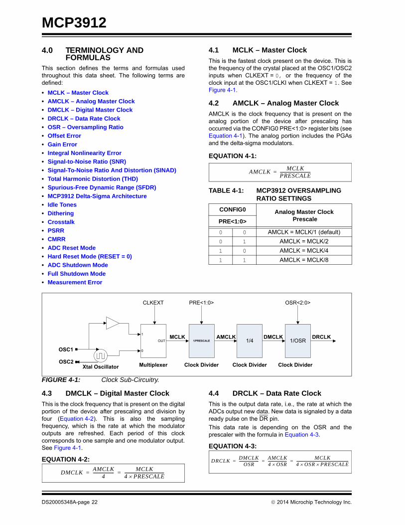
This is the fastest clock present on the device. This isthe frequency of the crystal placed at the OSC1/OSC2inputs when CLKEXT = 0, or the frequency of theclock input at the OSC1/CLKI when CLKEXT = 1. SeeFigure 4-1.
4.2 AMCLK – Analog Master Clock
AMCLK is the clock frequency that is present on theanalog portion of the device after prescaling hasoccurred via the CONFIG0 PRE<1:0> register bits (seeEquation 4-1). The analog portion includes the PGAsand the delta-sigma modulators.
EQUATION 4-1:
FIGURE 4-1: Clock Sub-Circuitry.
4.3 DMCLK – Digital Master Clock
This is the clock frequency that is present on the digitalportion of the device after prescaling and division byfour (Equation 4-2). This is also the samplingfrequency, which is the rate at which the modulatoroutputs are refreshed. Each period of this clockcorresponds to one sample and one modulator output.See Figure 4-1.
EQUATION 4-2:
4.4 DRCLK – Data Rate Clock
This is the output data rate, i.e., the rate at which theADCs output new data. New data is signaled by a dataready pulse on the DR pin.
This data rate is depending on the OSR and theprescaler with the formula in Equation 4-3.
EQUATION 4-3:
TABLE 4-1: MCP3912 OVERSAMPLING RATIO SETTINGS
CONFIG0 Analog Master Clock Prescale PRE<1:0>
0 0 AMCLK = MCLK/1 (default)
0 1 AMCLK = MCLK/2
1 0 AMCLK = MCLK/4
1 1 AMCLK = MCLK/8
AMCLKMCLK
PRESCALE-------------------------------=
Xtal Oscillator
MCLK
OSC1
OSC2 Multiplexer
OUT
0
1
1/PRESCALE 1/4 1/OSRAMCLK DMCLK DRCLK
Clock Divider Clock Divider Clock Divider
OSR<2:0>PRE<1:0>CLKEXT
DMCLKAMCLK
4---------------------
MCLK4 PRESCALE----------------------------------------= =
DRCLKDMCLK
OSR----------------------
AMCLK4 OSR---------------------
MCLK4 OSR PRESCALE-----------------------------------------------------------= = =
DS20005348A-page 22 2014 Microchip Technology Inc.

MCP3912
Since this is the output data rate, and because thedecimation filter is a SINC (or notch) filter, there is anotch in the filter transfer function at each integermultiple of this rate.
Table 4-2 describes the various combinations of OSRand PRESCALE, and their associated AMCLK,DMCLK and DRCLK rates.
TABLE 4-2: DEVICE DATA RATES IN FUNCTION OF MCLK, OSR AND PRESCALE, MCLK = 4 MHZ
PRE<1:0> OSR<2:0> OSR AMCLK DMCLK DRCLKDRCLK(ksps)
SINAD(dB)
Note 1
ENOB from
SINAD(bits)
Note 1
1 1 1 1 1 4096 MCLK/8 MCLK/32 MCLK/131072 .035 102.5 16.7
1 1 1 1 1 2048 MCLK/8 MCLK/32 MCLK/65536 .061 100 16.3
1 1 1 1 1 1024 MCLK/8 MCLK/32 MCLK/32768 .122 97 15.8
1 1 1 1 1 512 MCLK/8 MCLK/32 MCLK/16384 .244 96 15.6
1 1 0 1 1 256 MCLK/8 MCLK/32 MCLK/8192 0.488 94 15.3
1 1 0 1 0 128 MCLK/8 MCLK/32 MCLK/4096 0.976 90 14.7
1 1 0 0 1 64 MCLK/8 MCLK/32 MCLK/2048 1.95 83 13.5
1 1 0 0 0 32 MCLK/8 MCLK/32 MCLK/1024 3.9 70 11.3
1 0 1 1 1 4096 MCLK/4 MCLK/16 MCLK/65536 .061 102.5 16.7
1 0 1 1 1 2048 MCLK/4 MCLK/16 MCLK/32768 .122 100 16.3
1 0 1 1 1 1024 MCLK/4 MCLK/16 MCLK/16384 .244 97 15.8
1 0 1 1 1 512 MCLK/4 MCLK/16 MCLK/8192 .488 96 15.6
1 0 0 1 1 256 MCLK/4 MCLK/16 MCLK/4096 0.976 94 15.3
1 0 0 1 0 128 MCLK/4 MCLK/16 MCLK/2048 1.95 90 14.7
1 0 0 0 1 64 MCLK/4 MCLK/16 MCLK/1024 3.9 83 13.5
1 0 0 0 0 32 MCLK/4 MCLK/16 MCLK/512 7.8125 70 11.3
0 1 1 1 1 4096 MCLK/2 MCLK/8 MCLK/32768 .122 102.5 16.7
0 1 1 1 1 2048 MCLK/2 MCLK/8 MCLK/16384 .244 100 16.3
0 1 1 1 1 1024 MCLK/2 MCLK/8 MCLK/8192 .488 97 15.8
0 1 1 1 1 512 MCLK/2 MCLK/8 MCLK/4096 .976 96 15.6
0 1 0 1 1 256 MCLK/2 MCLK/8 MCLK/2048 1.95 94 15.3
0 1 0 1 0 128 MCLK/2 MCLK/8 MCLK/1024 3.9 90 14.7
0 1 0 0 1 64 MCLK/2 MCLK/8 MCLK/512 7.8125 83 13.5
0 1 0 0 0 32 MCLK/2 MCLK/8 MCLK/256 15.625 70 11.3
0 0 1 1 1 4096 MCLK MCLK/4 MCLK/16384 .244 102.5 16.7
0 0 1 1 0 2048 MCLK MCLK/4 MCLK/8192 .488 100 16.3
0 0 1 0 1 1024 MCLK MCLK/4 MCLK/4096 .976 97 15.8
0 0 1 0 0 512 MCLK MCLK/4 MCLK/2048 1.95 96 15.6
0 0 0 1 1 256 MCLK MCLK/4 MCLK/1024 3.9 94 15.3
0 0 0 1 0 128 MCLK MCLK/4 MCLK/512 7.8125 90 14.7
0 0 0 0 1 64 MCLK MCLK/4 MCLK/256 15.625 83 13.5
0 0 0 0 0 32 MCLK MCLK/4 MCLK/128 31.25 70 11.3
Note 1: For OSR = 32 and 64, DITHER = None. For OSR = 128 and higher, DITHER = Maximum. The SINADvalues are given from GAIN = 1.
2014 Microchip Technology Inc. DS20005348A-page 23
MCP3912
4.5 OSR – Oversampling Ratio
This is the ratio of the sampling frequency to the outputdata rate; OSR = DMCLK/DRCLK. The defaultOSR<2:0> is 256, or with MCLK = 4 MHz,PRESCALE = 1, AMCLK = 4 MHz, fS = 1 MHz andfD = 3.90625 ksps. The OSR<2:0> bits in Table 4-3 inthe CONFIG0 register are used to change theoversampling ratio (OSR).
4.6 Offset Error
This is the error induced by the ADC when the inputsare shorted together (VIN = 0V). The specificationincorporates both PGA and ADC offset contributions.This error varies with PGA and OSR settings. Theoffset is different on each channel and varies from chip-to-chip. The offset is specified in µV. The offset errorcan be digitally compensated independently on eachchannel through the OFFCAL_CHn registers with a24-bit calibration word.
The offset on the MCP3912 has a low-temperaturecoefficient.
4.7 Gain Error
This is the error induced by the ADC on the slope of thetransfer function. It is the deviation expressed in a per-centage, compared to the ideal transfer functiondefined in Equation 5-3. The specification incorporatesboth PGA and ADC gain error contributions, but not theVREF contribution (it is measured with an externalVREF).
This error varies with PGA and OSR settings. The gainerror can be digitally compensated independently oneach channel through the GAINCAL_CHn registerswith a 24-bit calibration word.
The gain error on the MCP3912 has a low temperaturecoefficient.
4.8 Integral Nonlinearity Error
Integral nonlinearity error is the maximum deviation ofan ADC transition point from the corresponding point ofan ideal transfer function, with the offset and gainerrors removed or with the end points equal to zero.
It is the maximum remaining error after calibration ofoffset and gain errors for a DC input signal.
4.9 Signal-to-Noise Ratio (SNR)
For the MCP3912 ADCs, the signal-to-noise ratio is aratio of the output fundamental signal power to thenoise power (not including the harmonics of the signal)when the input is a sine wave at a predeterminedfrequency (see Equation 4-4). It is measured in dB.Usually, only the maximum signal-to-noise ratio isspecified. The SNR figure depends mainly on the OSRand DITHER settings of the device.
EQUATION 4-4: SIGNAL-TO-NOISE RATIO
4.10 Signal-To-Noise Ratio And Distortion (SINAD)
The most important Figure of Merit for analogperformance of the ADCs present on the MCP3912 isthe Signal-to-Noise And Distortion (SINAD)specification.
The Signal-to-Noise And Distortion ratio is similar tosignal-to-noise ratio, with the exception that you mustinclude the harmonic’s power in the noise powercalculation (see Equation 4-5). The SINADspecification depends mainly on the OSR and DITHERsettings.
EQUATION 4-5: SINAD EQUATION
The calculated combination of SNR and THD per thefollowing formula also yields SINAD (see Equation 4-6).
EQUATION 4-6: SINAD, THD AND SNR RELATIONSHIP
TABLE 4-3: MCP3912 OVERSAMPLING RATIO SETTINGS
OSR<2:0>Oversampling Ratio
OSR
0 0 0 32
0 0 1 64
0 1 0 128
0 1 1 256 (Default)
1 0 0 512
1 0 1 1024
1 1 0 2048
1 1 1 4096SNR dB 10
SignalPowerNoisePower---------------------------------- log=
SINAD dB 10SignalPower
Noise HarmonicsPower+--------------------------------------------------------------------- log=
SINAD dB 10 10
SNR10
-----------
10
THD–10
----------------
+log=
DS20005348A-page 24 2014 Microchip Technology Inc.

MCP3912
4.11 Total Harmonic Distortion (THD)
The total harmonic distortion is the ratio of the outputharmonics power to the fundamental signal power for asine wave input, and is defined in Equation 4-7.
EQUATION 4-7:
The THD calculation includes the first 35 harmonics forthe MCP3912 specifications. The THD is usuallymeasured only with respect to the ten first harmonics,which leads artificially to better figures. THD issometimes expressed in a percentage. Equation 4-8converts the THD in percentages.
EQUATION 4-8:
This specification depends mainly on the DITHERsetting.
4.12 Spurious-Free Dynamic Range (SFDR)
Spurious-Free Dynamic Range, or SFDR, is the ratiobetween the output power of the fundamental and thehighest spur in the frequency spectrum (seeEquation 4-9). The spur frequency is not necessarily aharmonic of the fundamental, even though it is usuallythe case. This figure represents the dynamic range ofthe ADC when a full-scale signal is used at the input.This specification depends mainly on the DITHERsetting.
EQUATION 4-9:
4.13 MCP3912 Delta-Sigma Architecture
The MCP3912 incorporates four delta-sigma ADCswith a multi-bit architecture. A delta-sigma ADC is anoversampling converter that incorporates a built-inmodulator, which digitizes the quantity of chargesintegrated by the modulator loop (see Figure 5-1). Thequantizer is the block that is performing theanalog-to-digital conversion. The quantizer is typically1-bit, or a simple comparator, which helps maintain thelinearity performance of the ADC (the DAC structure is,in this case, inherently linear).
Multi-bit quantizers help to lower the quantization error(the error fed back in the loop can be very large with1-bit quantizers) without changing the order of themodulator or the OSR, which leads to better SNRfigures. However, typically, the linearity of sucharchitectures is more difficult to achieve since the DAClinearity is as difficult to attain, and its linearity limits theTHD of such ADCs.
The quantizer present in each ADC channel in theMCP3912 is a Flash ADC composed of fourcomparators arranged with equally spaced thresholdsand a thermometer coding. The MCP3912 alsoincludes proprietary five-level DAC architecture that isinherently linear for improved THD figures.
4.14 Idle Tones
A delta-sigma converter is an integrating converter. Italso has a finite quantization step (LSB) that can bedetected by its quantizer. A DC input voltage that isbelow the quantization step should only provide anall zeros result, since the input is not large enough tobe detected. As an integrating device, any delta-sigmaADC will show idle tones. This means that the outputwill have spurs in the frequency content that depend onthe ratio between quantization step voltage and theinput voltage. These spurs are the result of theintegrated sub-quantization step inputs that willeventually cross the quantization steps after a longenough integration. This will induce an AC frequency atthe output of the ADC, and can be shown in the ADCoutput spectrum.
These idle tones are residues that are inherent to thequantization process and the fact that the converter isintegrating at all times without being reset. They areresidues of the finite resolution of the conversionprocess. They are very difficult to attenuate and theyare heavily signal dependent. They can degrade theSFDR and THD of the converter, even for DC inputs.They can be localized in the baseband of the converterand are thus difficult to filter from the actual input signal.
For power metering applications, idle tones can be verydisturbing, because energy can be detected even atthe 50 or 60 Hz frequency, depending on the DC offsetof the ADCs, while no power is really present at theinputs. The only practical way to suppress or attenuatethe idle tones phenomenon is to apply dithering to theADC. The amplitudes of the idle tones are a function ofthe order of the modulator, the OSR and the number oflevels in the quantizer of the modulator. A higher order,a higher OSR or a higher number of levels for thequantizer will attenuate the amplitudes of the idletones.
THD dB 10HarmonicsPower
FundamentalPower----------------------------------------------------- log=
THD % 100 10THD dB
20------------------------
=
SFDR dB 10FundamentalPowerHighestSpurPower----------------------------------------------------- log=
2014 Microchip Technology Inc. DS20005348A-page 25

MCP3912
4.15 Dithering
In order to suppress or attenuate the idle tones presentin any delta-sigma ADCs, dithering can be applied tothe ADC. Dithering is the process of adding an error tothe ADC feedback loop in order to “decorrelate” theoutputs and “break” the idle tone’s behavior. Usually arandom or pseudo-random generator adds an analogor digital error to the feedback loop of the delta-sigmaADC in order to ensure that no tonal behavior canhappen at its outputs. This error is filtered by the feed-back loop and typically has a zero average value sothat the converter static transfer function is not dis-turbed by the dithering process. However, the ditheringprocess slightly increases the noise floor (it adds noiseto the part) while reducing its tonal behavior and thusimproving SFDR and THD. The dithering processscrambles the idle tones into baseband white noise andensures that dynamic specs (SNR, SINAD, THD,SFDR) are less signal dependent. The MCP3912 incor-porates a proprietary dithering algorithm on all ADCs inorder to remove idle tones and improve THD, which iscrucial for power metering applications.
4.16 Crosstalk
Crosstalk is defined as the perturbation caused on oneADC channel by all the other ADC channels present inthe chip. It is a measurement of the isolation betweeneach channel present in the chip.
This measurement is a two-step procedure:
1. Measure one ADC input with no perturbation onthe other ADC (ADC inputs shorted).
2. Measure the same ADC input with aperturbation sine wave signal on all the otherADCs at a certain predefined frequency.
Crosstalk is the ratio between the output power of theADC when the perturbation is and is not present,divided by the power of the perturbation signal. A lowercrosstalk value implies more independence andisolation between the channels.
The measurement of this signal is performed under thedefault conditions of MCLK = 4 MHz:
• GAIN = 1• PRESCALE = 1• OSR = 256
• MCLK = 4 MHz
Step 1 for CH0 Crosstalk Measurement:
• CH0+ = CH0- = AGND
• CHn+ = CHn- = AGND n comprised between 1 and 3
Step 2 for CH0 Crosstalk Measurement:
• CH0+ = CH0-=AGND
• CHn+ - CHn- = 1.2VP-P @ 50/60 Hz (full-scale sine wave), n comprised between 1 and 3
The crosstalk for Channel 0 is then calculated with theformula in Equation 4-10.
EQUATION 4-10:
The crosstalk depends slightly on the position of thechannels in the MCP3912 device. This dependency isshown in the Figure 2-32, where the inner channelsshow more crosstalk than the outer channels, sincethey are located closer to the perturbation sources. Theouter channels have the preferred locations tominimize crosstalk.
4.17 PSRRThis is the ratio between a change in the power supplyvoltage and the ADC output codes. It measures the influ-ence of the power supply voltage on the ADC outputs.
The PSRR specification can be DC (the power supplyis taking multiple DC values) or AC (the power supplyis a sine wave at a certain frequency with a certaincommon mode). In AC, the amplitude of the sine waverepresents the change in the power supply. It is definedin Equation 4-11.
EQUATION 4-11:
Where: VOUT is the equivalent input voltage that theoutput code translates to, with the ADC transferfunction.
In the MCP3912 specification for DC PSRR, AVDD var-ies from 2.7V to 3.6V, and for AC PSRR, a 50/60 Hzsine wave is chosen centered around 3.0V with amaximum 300 mV amplitude. The PSRR specificationis measured with AVDD = DVDD.
4.18 CMRR
CMRR is the ratio between a change in thecommon-mode input voltage and the ADC outputcodes. It measures the influence of the common-modeinput voltage on the ADC outputs.
The CMRR specification can be DC (thecommon-mode input voltage is taking multiple DCvalues) or AC (the common-mode input voltage is asine wave at a certain frequency with a certain commonmode). In AC, the amplitude of the sine waverepresents the change in the power supply. It is definedin Equation 4-12.
CTalk dB 10CH0PowerCHnPower--------------------------------- log=
PSRR dB 20VOUT
AVDD------------------- log=
DS20005348A-page 26 2014 Microchip Technology Inc.
MCP3912
EQUATION 4-12:
Where: VCM = (CHn+ + CHn-)/2 is the common-modeinput voltage, and VOUT is the equivalent input voltagethat the output code translates to, with the ADC transferfunction.
In the MCP3912 specification, VCM varies from -1V to+1V.
4.19 ADC Reset Mode
ADC Reset mode (also called Soft Reset mode) canonly be entered through setting the RESET<3:0> bitshigh in the Configuration register. This mode is definedas the condition where the converters are active, buttheir output is forced to 0.
The Flash ADC output of the corresponding channelwill be reset to its default value (0011) in the MODregister.
The ADCs can immediately output meaningful codesafter leaving Reset mode (and after the sinc filtersettling time). This mode is both entered and exitedthrough bit settings in the Configuration register.
Each converter can be placed in Soft Reset modeindependently. The Configuration registers are notmodified by the Soft Reset mode. A data ready pulsewill not be generated by an ADC channel in Resetmode.
When an ADC exits ADC Reset mode, any phase delaypresent before Reset was entered will still be present.If one ADC was not in Reset, the ADC leaving Resetmode will automatically resynchronize the phase delayrelative to the other ADC channel per the phase delayregister block, and give data ready pulses accordingly.
If an ADC is placed in Reset mode while others areconverting, it does not shut down the internal clock.When coming out of reset, it will be automaticallyresynchronized with the clock, which did not stopduring Reset.
If all ADCs are in Soft Reset mode, the clock is nolonger distributed to the digital core for low-poweroperation. Once any of the ADCs are back to normaloperation, the clock is automatically distributed again.
However, when the four channels are in Soft Resetmode, the input structure is still clocking if MCLK isapplied in order to properly bias the inputs so that noleakage current is observed. If MCLK is not applied,large analog input leakage currents can be observedfor highly negative input voltages (typically below -0.6Vreferred to AGND).
4.20 Hard Reset Mode (RESET = 0)
This mode is only available during a POR or when theRESET pin is pulled logic low. The RESET pin logic-lowstate places the device in Hard Reset mode. In thismode, all internal registers are reset to their defaultstate.
The DC biases for the analog blocks are still active, i.e.,the MCP3912 is ready to convert. However, this pinclears all conversion data in the ADCs. Thecomparators’ outputs of all ADCs are forced to theirReset state (0011). The SINC filters are all reset, aswell as their double output buffers. The Hard Resetmode requires a minimum pulse low time (seeSection 1.0 “Electrical Characteristics”). During aHard Reset, no communication with the part ispossible. The digital interface is maintained in a Resetstate.
During this state, the clock MCLK can be applied to thepart in order to properly bias the input structures of allchannels. If not applied, large analog input leakagecurrents can be observed for highly negative inputsignals and, after removing the Hard Reset state, acertain start-up time is necessary to bias the inputstructure properly. During this delay, the ADCconversions can be inaccurate.
4.21 ADC Shutdown Mode
ADC Shutdown mode is defined as a state where theconverters and their biases are off, consuming onlyleakage current. When one of the SHUTDOWN<3:0>bits is reset to ‘0’, the analog biases of thecorresponding channel will be enabled, as well as theclock and the digital circuitry. The ADC of thecorresponding channel will give a data ready after theSINC filter settling time has occurred. However, sincethe analog biases are not completely settled at thebeginning of the conversion, the sampling may not beaccurate during about 1 ms (corresponding to thesettling time of the biasing in worst-case conditions). Inorder to ensure accuracy, the data ready pulse withinthe delay of 1 ms + settling time of the SINC filtershould be discarded.
Each converter can be placed in Shutdown modeindependently. The configuration registers are notmodified by the Shutdown mode. This mode is onlyavailable through programming the SHUTDOWN<3:0>bits of the CONFIG1 register.
The output data is flushed to all zeros while in ADCShutdown mode. No data ready pulses are generatedby any ADC while in ADC Shutdown mode.
CMRR dB 20VOUT
VCM----------------- log=
2014 Microchip Technology Inc. DS20005348A-page 27
MCP3912
When an ADC exits ADC Shutdown mode, any phasedelay present before shutdown was entered will still bepresent. If one ADC was not in Shutdown, the ADCleaving Shutdown mode will automatically resynchro-nize the phase delay relative to the other ADC channelper the phase delay register block and give data readypulses accordingly.
If an ADC is placed in Shutdown mode while others areconverting, it does not shut down the internal clock.When coming back out of Shutdown mode, it willautomatically be resynchronized with the clock that didnot stop during reset.
If all ADCs are in ADC Shutdown mode, the clock is notdistributed to the input structure or to the digital core forlow-power operation. This can potentially cause highanalog input leakage currents at the analog inputs if theinput voltage is highly negative (typically below -0.6Vreferred to AGND). Once either of the ADCs is back tonormal operation, the clock is automatically distributedagain.
4.22 Full Shutdown Mode
The lowest power consumption can be achieved whenSHUTDOWN<3:0> = 1111,VREFEXT = CLKEXT = 1. This mode is called FullShutdown mode, and no analog circuitry is enabled. Inthis mode, both AVDD and DVDD POR monitoring arealso disabled and no clock is propagated throughoutthe chip. All ADCs are in Shutdown mode, and theinternal voltage reference is disabled. This mode doesnot reset the writable part of the register map to itsdefault values.
The clock is no longer distributed to the input structure aswell. This can potentially cause high analog input leak-age currents at the analog inputs if the input voltage ishighly negative (typically below -0.6V referred to AGND).
The only circuit that remains active is the SPI interface,but this circuit does not induce any static powerconsumption. If SCK is idle, the only currentconsumption comes from the leakage currents inducedby the transistors.
This mode can be used to power-down the chipcompletely and avoid power consumption when thereis no data to convert at the analog inputs. Any SCK orMCLK edge occurring while in this mode will inducedynamic power consumption.
Once any of the SHUTDOWN<3:0>, CLKEXT andVREFEXT bits return to ‘0’, the two POR monitoringblocks are operational and AVDD and DVDD monitoringcan take place.
4.23 Measurement Error
The measurement error specification is typically usedin power meter applications. This specification is ameasurement of the linearity of the active energy of agiven power meter across its dynamic range.
For this measurement, the goal is to measure theactive energy of one phase when the voltage RootMean Square (RMS) value is fixed and the currentRMS value is sweeping across the dynamic rangespecified by the meter. The measurement error is thenonlinearity error of the energy power across thecurrent dynamic range. It is expressed as apercentage. Equation 4-13 shows the formula thatcalculates the measurement error:
EQUATION 4-13:
In the present device, the calculation of the active energyis done externally as a post-processing step that typicallyhappens in the microcontroller, considering, for example,the even channels as current channels and the oddchannels as voltage channels. The odd channels(voltages) are fed with a full-scale sine wave at 600 mVpeak, and are configured with GAIN = 1 andDITHER = Maximum. To obtain the active energymeasurement error graphs, the even channels are fedwith sine waves with amplitudes that vary from 600 mVpeak to 60 µV peak, representing a 10000:1 dynamicrange. The offset is removed on both current and voltagechannels, and the channels are multiplied together to giveinstantaneous power. The active energy is calculated bymultiplying the current and voltage channel, andaveraging the results of this power during 20 seconds toextract the active energy. The sampling frequency ischosen as a multiple integer of line frequency (coherentsampling). Therefore, the calculation does not take intoaccount any residue coming from bad synchronization.
The measurement error is a function of IRMS and varieswith the OSR, averaging time and MCLK frequency,and is tightly coupled with the noise and linearityspecifications. The measurement error is a function ofthe linearity and THD of the ADCs, while the standarddeviation of the measurement error is a function of thenoise specification of the ADCs. Overall, the low THDspecification enables low measurement error on a verylarge dynamic range (e.g. 10,000:1). A low noise andhigh SNR specification enables the decreasing of themeasurement time and, therefore, the calibration time,to obtain a reliable measurement error specification.
Figure 2-5 shows the typical measurement error curvesobtained with the samples acquired by the MCP3912,using the default settings with a 1-point and 2-point cal-ibration. These calibrations are detailed in Section 7.0“Basic Application Recommendations”.
Measurement Error IRMS Measured Active Energy Active Energy present at inputs–Active Energy present at inputs
-------------------------------------------------------------------------------------------------------------------------------------------- 100%=
DS20005348A-page 28 2014 Microchip Technology Inc.

MCP3912
NOTES:
2014 Microchip Technology Inc. DS20005348A-page 29
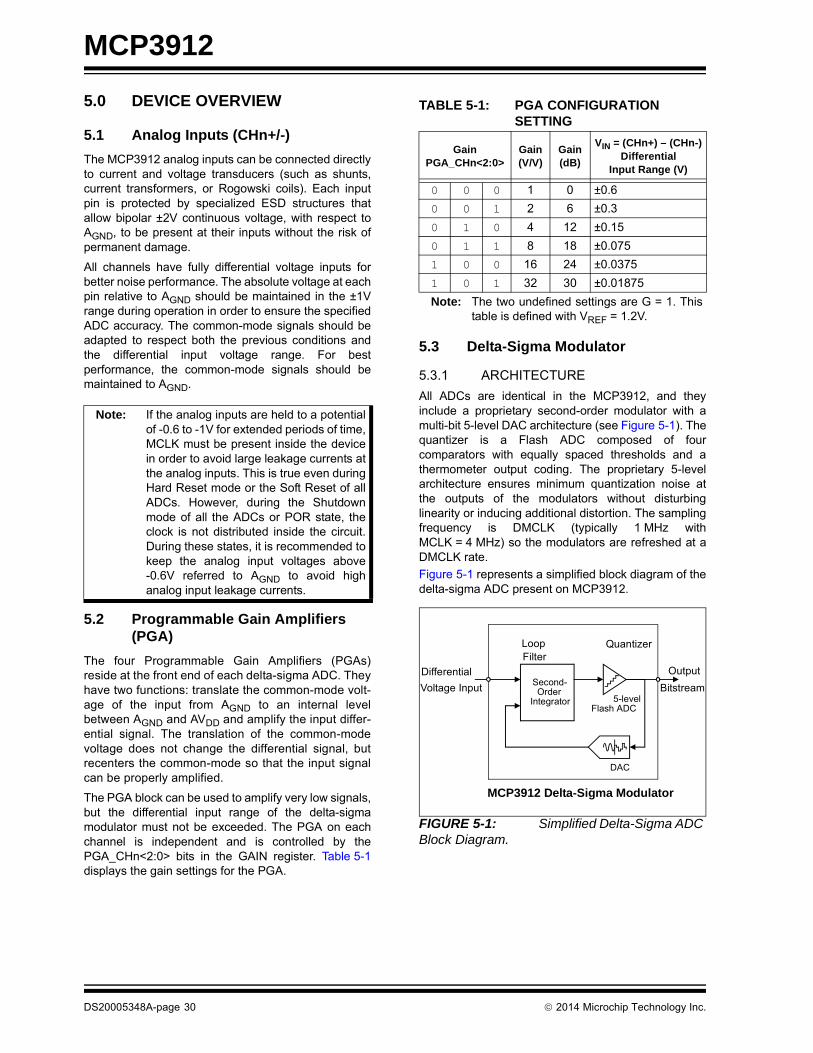
MCP3912
5.0 DEVICE OVERVIEW
5.1 Analog Inputs (CHn+/-)
The MCP3912 analog inputs can be connected directlyto current and voltage transducers (such as shunts,current transformers, or Rogowski coils). Each inputpin is protected by specialized ESD structures thatallow bipolar ±2V continuous voltage, with respect toAGND, to be present at their inputs without the risk ofpermanent damage.
All channels have fully differential voltage inputs forbetter noise performance. The absolute voltage at eachpin relative to AGND should be maintained in the ±1Vrange during operation in order to ensure the specifiedADC accuracy. The common-mode signals should beadapted to respect both the previous conditions andthe differential input voltage range. For bestperformance, the common-mode signals should bemaintained to AGND.
5.2 Programmable Gain Amplifiers (PGA)
The four Programmable Gain Amplifiers (PGAs)reside at the front end of each delta-sigma ADC. Theyhave two functions: translate the common-mode volt-age of the input from AGND to an internal levelbetween AGND and AVDD and amplify the input differ-ential signal. The translation of the common-modevoltage does not change the differential signal, butrecenters the common-mode so that the input signalcan be properly amplified.
The PGA block can be used to amplify very low signals,but the differential input range of the delta-sigmamodulator must not be exceeded. The PGA on eachchannel is independent and is controlled by thePGA_CHn<2:0> bits in the GAIN register. Table 5-1displays the gain settings for the PGA.
5.3 Delta-Sigma Modulator
5.3.1 ARCHITECTURE
All ADCs are identical in the MCP3912, and theyinclude a proprietary second-order modulator with amulti-bit 5-level DAC architecture (see Figure 5-1). Thequantizer is a Flash ADC composed of fourcomparators with equally spaced thresholds and athermometer output coding. The proprietary 5-levelarchitecture ensures minimum quantization noise atthe outputs of the modulators without disturbinglinearity or inducing additional distortion. The samplingfrequency is DMCLK (typically 1 MHz withMCLK = 4 MHz) so the modulators are refreshed at aDMCLK rate.
Figure 5-1 represents a simplified block diagram of thedelta-sigma ADC present on MCP3912.
FIGURE 5-1: Simplified Delta-Sigma ADC Block Diagram.
Note: If the analog inputs are held to a potentialof -0.6 to -1V for extended periods of time,MCLK must be present inside the devicein order to avoid large leakage currents atthe analog inputs. This is true even duringHard Reset mode or the Soft Reset of allADCs. However, during the Shutdownmode of all the ADCs or POR state, theclock is not distributed inside the circuit.During these states, it is recommended tokeep the analog input voltages above-0.6V referred to AGND to avoid highanalog input leakage currents.
TABLE 5-1: PGA CONFIGURATION SETTING
Gain PGA_CHn<2:0>
Gain(V/V)
Gain(dB)
VIN = (CHn+) – (CHn-)Differential
Input Range (V)
0 0 0 1 0 ±0.6
0 0 1 2 6 ±0.3
0 1 0 4 12 ±0.15
0 1 1 8 18 ±0.075
1 0 0 16 24 ±0.0375
1 0 1 32 30 ±0.01875
Note: The two undefined settings are G = 1. Thistable is defined with VREF = 1.2V.
Second-Order
Integrator
LoopFilter
Quantizer
DAC
Differential
Voltage Input
Output
Bitstream5-level
Flash ADC
MCP3912 Delta-Sigma Modulator
DS20005348A-page 30 2014 Microchip Technology Inc.

MCP3912
5.3.2 MODULATOR INPUT RANGE AND SATURATION POINT
For a specified voltage reference value of 1.2V, thespecified differential input range is ±600 mV. The inputrange is proportional to VREF and scales according tothe VREF voltage. This range ensures the stability of themodulator over amplitude and frequency. Outside ofthis range, the modulator is still functional; however, itsstability is no longer ensured and therefore it is notrecommended to exceed this limit. The saturation pointfor the modulator is VREF/1.5, since the transferfunction of the ADC includes a gain of 1.5 by default(independent from the PGA setting). See Section 5.5“ADC Output Coding”).
5.3.3 BOOST SETTINGS
The delta-sigma modulators include a programmablebiasing circuit in order to further adjust the powerconsumption to the sampling speed applied throughthe MCLK. This can be programmed through theBOOST<1:0> bits, which are applied to all channelssimultaneously.
The maximum achievable analog master clock speed(AMCLK), the maximum sampling frequency (DMCLK)and the maximum achievable data rate (DRCLK),highly depend on BOOST<1:0> and PGA_CHn<2:0>settings. Table 5-2 specifies the maximum AMCLKpossible to keep optimal accuracy in the function ofBOOST<1:0> and PGA_CHn<2:0> settings.
TABLE 5-2: MAXIMUM AMCLK LIMITS AS A FUNCTION OF BOOST AND PGA GAIN
ConditionsVDD = 3.0V to 3.6V,
TA from -40°C to +125°CVDD = 2.7V to 3.6V,
TA from -40°C to +125°C
Boost Gain
Maximum AMCLK(MHz)
(SINAD within -3 dB from its maximum)
Maximum AMCLK (MHz)
(SINAD within -5 dB from its maximum)
Maximum AMCLK (MHz)
(SINAD within -3 dB from its maximum)
Maximum AMCLK (MHz)
(SINAD within -5 dB from its maximum)
0.5x 1 4 4 4 4
0.66x 1 6.4 7.3 6.4 7.3
1x 1 11.4 11.4 10.6 10.6
2x 1 16 16 16 16
0.5x 2 4 4 4 4
0.66x 2 6.4 7.3 6.4 7.3
1x 2 11.4 11.4 10.6 10.6
2x 2 16 16 13.3 14.5
0.5x 4 2.9 2.9 2.9 2.9
0.66x 4 6.4 6.4 6.4 6.4
1x 4 10.7 10.7 9.4 10.7
2x 4 16 16 16 16
0.5x 8 2.9 4 2.9 4
0.66x 8 7.3 8 6.4 7.3
1x 8 11.4 12.3 8 8.9
2x 8 16 16 10 11.4
0.5x 16 2.9 2.9 2.9 2.9
0.66x 16 6.4 7.3 6.4 7.3
1x 16 11.4 11.4 9.4 10.6
2x 16 13.3 16 8.9 11.4
0.5x 32 2.9 2.9 2.9 2.9
0.66x 32 7.3 7.3 7.3 7.3
1x 32 10.6 12.3 9.4 10,6
2x 32 13.3 16 10 11.4
2014 Microchip Technology Inc. DS20005348A-page 31
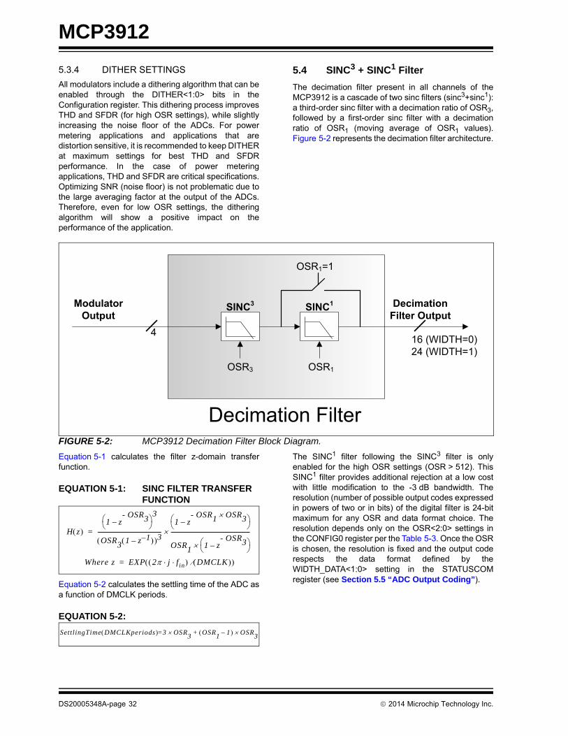
MCP3912
5.3.4 DITHER SETTINGS
All modulators include a dithering algorithm that can beenabled through the DITHER<1:0> bits in theConfiguration register. This dithering process improvesTHD and SFDR (for high OSR settings), while slightlyincreasing the noise floor of the ADCs. For powermetering applications and applications that aredistortion sensitive, it is recommended to keep DITHERat maximum settings for best THD and SFDRperformance. In the case of power meteringapplications, THD and SFDR are critical specifications.Optimizing SNR (noise floor) is not problematic due tothe large averaging factor at the output of the ADCs.Therefore, even for low OSR settings, the ditheringalgorithm will show a positive impact on theperformance of the application.
5.4 SINC3 + SINC1 Filter
The decimation filter present in all channels of theMCP3912 is a cascade of two sinc filters (sinc3+sinc1):a third-order sinc filter with a decimation ratio of OSR3,followed by a first-order sinc filter with a decimationratio of OSR1 (moving average of OSR1 values).Figure 5-2 represents the decimation filter architecture.
FIGURE 5-2: MCP3912 Decimation Filter Block Diagram.
Equation 5-1 calculates the filter z-domain transferfunction.
EQUATION 5-1: SINC FILTER TRANSFER FUNCTION
Equation 5-2 calculates the settling time of the ADC asa function of DMCLK periods.
EQUATION 5-2:
The SINC1 filter following the SINC3 filter is onlyenabled for the high OSR settings (OSR > 512). ThisSINC1 filter provides additional rejection at a low costwith little modification to the -3 dB bandwidth. Theresolution (number of possible output codes expressedin powers of two or in bits) of the digital filter is 24-bitmaximum for any OSR and data format choice. Theresolution depends only on the OSR<2:0> settings inthe CONFIG0 register per the Table 5-3. Once the OSRis chosen, the resolution is fixed and the output coderespects the data format defined by theWIDTH_DATA<1:0> setting in the STATUSCOMregister (see Section 5.5 “ADC Output Coding”).
ModulatorOutput
SINC3 SINC1 DecimationFilter Output
OSR3 OSR1
416 (WIDTH=0)24 (WIDTH=1)
Decimation Filter
OSR1=1
H z 1 z
- OSR3–
3
OSR3 1 z 1–– 3----------------------------------------------
1 z- OSR1 OSR3
–
OSR1 1 z- OSR3–
---------------------------------------------------------=
Where z EXP 2 j fin DMCLK =
SettlingTime DMCLKperiods 3 OSR3 OSR1 1– OSR3+=
DS20005348A-page 32 2014 Microchip Technology Inc.
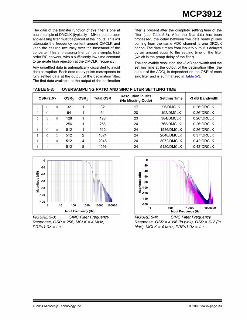
MCP3912
The gain of the transfer function of this filter is one ateach multiple of DMCLK (typically 1 MHz), so a properanti-aliasing filter must be placed at the inputs. This willattenuate the frequency content around DMCLK andkeep the desired accuracy over the baseband of theconverter. This anti-aliasing filter can be a simple, first-order RC network, with a sufficiently low time constantto generate high rejection at the DMCLK frequency.Any unsettled data is automatically discarded to avoiddata corruption. Each data ready pulse corresponds tofully settled data at the output of the decimation filter.The first data available at the output of the decimation
filter is present after the complete settling time of thefilter (see Table 5-3). After the first data has beenprocessed, the delay between two data ready pulsescoming from the same ADC channel is one DRCLKperiod. The data stream from input to output is delayedby an amount equal to the settling time of the filter(which is the group delay of the filter).
The achievable resolution, the -3 dB bandwidth and thesettling time at the output of the decimation filter (theoutput of the ADC), is dependent on the OSR of eachsinc filter and is summarized in Table 5-3.
FIGURE 5-3: SINC Filter Frequency Response, OSR = 256, MCLK = 4 MHz, PRE<1:0> = 00.
FIGURE 5-4: SINC Filter Frequency Response, OSR = 4096 (in pink), OSR = 512 (in blue), MCLK = 4 MHz, PRE<1:0> = 00.
TABLE 5-3: OVERSAMPLING RATIO AND SINC FILTER SETTLING TIME
OSR<2:0> OSR3 OSR1 Total OSRResolution in Bits (No Missing Code)
Settling Time -3 dB Bandwidth
0 0 0 32 1 32 17 96/DMCLK 0.26*DRCLK
0 0 1 64 1 64 20 192/DMCLK 0.26*DRCLK
0 1 0 128 1 128 23 384/DMCLK 0.26*DRCLK
0 1 1 256 1 256 24 768/DMCLK 0.26*DRCLK
1 0 0 512 1 512 24 1536/DMCLK 0.26*DRCLK
1 0 1 512 2 1024 24 2048/DMCLK 0.37*DRCLK
1 1 0 512 4 2048 24 3072/DMCLK 0.42*DRCLK
1 1 1 512 8 4096 24 5120/DMCLK 0.43*DRCLK
-80
-60
-40
-20
0
agni
tude
(dB
)
-120
-100
1 10 100 1000 10000 100000
Ma
Input Frequency (Hz)
-100
-80
-60
-40
-20
0
gnitu
de (d
B)
-160
-140
-120
1 100 10000 1000000
Ma
Input Frequency (Hz)
2014 Microchip Technology Inc. DS20005348A-page 33

MCP3912
5.5 ADC Output Coding
The second-order modulator, SINC3+SINC1 filter,PGA, VREF and the analog input structure all worktogether to produce the device transfer function for theanalog-to-digital conversion (see Equation 5-3).
Channel data is calculated on 24-bit (23-bit plus sign)and coded in two's complement format, MSB first. Theoutput format can then be modified by theWIDTH_DATA<1:0> settings in the STATUSCOMregister to allow 16-/24-/32-bit format compatibility (seeSection 8.5 “STATUSCOM Register – Status andCommunication Register” for more information).
In case of positive saturation (CHn+ – CHn-> VREF/1.5), the output is locked to 7FFFFF for 24-bit
mode. In case of negative saturation(CHn+ - CHn- < -VREF/1.5), the output code is lockedto 800000 for 24-bit mode.
Equation 5-3 is only true for DC inputs. For AC inputs,this transfer function needs to be multiplied by thetransfer function of the SINC3+SINC1 filter (seeEquation 5-1 and Equation 5-3).
EQUATION 5-3:
For other than the default 24-bit data formats,Equation 5-3 should be multiplied by a scaling factordepending on the data format used (defined byWIDTH_DATA<1:0>). The data format and associatedscaling factors are given in Figure 5-5.
FIGURE 5-5: Output Data Formats.
The ADC resolution is a function of the OSR(Section 5.4 “SINC3 + SINC1 Filter”). The resolutionis the same for all channels. No matter what theresolution is, the ADC output data is always calculatedin 24-bit words, with added zeros at the end if the OSRis not large enough to produce 24-bit resolution (leftjustification).
DATA_CHnCHn+ CHn-–
VREF+ VREF-–-----------------------------------------
8,388,608 G 1.5=
For 24-bit Mode, WIDTH_Data<1:0> = 01(Default)
DA
TA<7
>
WIDTH_DATA<1:0> = 1132-bit with sign extension
DATA<23>
DATA<23:16>
31 0DATA<15:8>
DATA<7:0>
WIDTH_DATA<1:0> = 1032-bit with zeros padded 0x00
31 0DATA
<23:16>DATA<7:0>
DATA<15:8>
WIDTH_DATA<1:0> = 0124-bit
DATA<23:16>
DATA<15:8>
DATA<7:0>
23 0
WIDTH_DATA<1:0> = 0016-bit
DATA<15:8>
15 0DATA
<23:16>Rounded
Unformatted ADC data DATA<23:16>
DATA<15:8>
DATA<7:0>
23 0
x1/256
x1
x256
x1
ScalingFactor
DS20005348A-page 34 2014 Microchip Technology Inc.

MCP3912
TABLE 5-4: OSR = 256 (AND HIGHER) OUTPUT CODE EXAMPLES
ADC Output Code (MSB First) HexadecimalDecimal,
24-bit Resolution
0 1 1 1 1 1 1 1 1 1 1 1 1 1 1 1 1 1 1 1 1 1 1 1 0x7FFFFF + 8,388,607
0 1 1 1 1 1 1 1 1 1 1 1 1 1 1 1 1 1 1 1 1 1 1 0 0x7FFFFE + 8,388,606
0 0 0 0 0 0 0 0 0 0 0 0 0 0 0 0 0 0 0 0 0 0 0 0 0x000000 0
1 1 1 1 1 1 1 1 1 1 1 1 1 1 1 1 1 1 1 1 1 1 1 1 0xFFFFFF -1
1 0 0 0 0 0 0 0 0 0 0 0 0 0 0 0 0 0 0 0 0 0 0 1 0x800001 - 8,388,607
1 0 0 0 0 0 0 0 0 0 0 0 0 0 0 0 0 0 0 0 0 0 0 0 0x800000 - 8,388,608
TABLE 5-5: OSR = 128 OUTPUT CODE EXAMPLES
ADC Output Code (MSB First) HexadecimalDecimal,
23-bit Resolution
0 1 1 1 1 1 1 1 1 1 1 1 1 1 1 1 1 1 1 1 1 1 1 0 0x7FFFFE + 4,194,303
0 1 1 1 1 1 1 1 1 1 1 1 1 1 1 0 1 1 1 1 1 1 0 0 0x7FFFFC + 4,194,302
0 0 0 0 0 0 0 0 0 0 0 0 0 0 0 0 0 0 0 0 0 0 0 0 0x000000 0
1 1 1 1 1 1 1 1 1 1 1 1 1 1 1 1 1 1 1 1 1 1 1 0 0xFFFFFE -1
1 0 0 0 0 0 0 0 0 0 0 0 0 0 0 0 0 0 0 0 0 0 1 0 0x800002 - 4,194,303
1 0 0 0 0 0 0 0 0 0 0 0 0 0 0 0 0 0 0 0 0 0 0 0 0x800000 - 4,194,304
TABLE 5-6: OSR = 64 OUTPUT CODE EXAMPLES
ADC Output code (MSB First) HexadecimalDecimal,
20-bit resolution
0 1 1 1 1 1 1 1 1 1 1 1 1 1 1 1 1 1 1 1 0 0 0 0 0x7FFFF0 + 524, 287
0 1 1 1 1 1 1 1 1 1 1 1 1 1 1 1 1 1 1 0 0 0 0 0 0x7FFFE0 + 524, 286
0 0 0 0 0 0 0 0 0 0 0 0 0 0 0 0 0 0 0 0 0 0 0 0 0x000000 0
1 1 1 1 1 1 1 1 1 1 1 1 1 1 1 1 1 1 1 1 0 0 0 0 0xFFFFF0 -1
1 0 0 0 0 0 0 0 0 0 0 0 0 0 0 0 0 0 0 1 0 0 0 0 0x800010 - 524,287
1 0 0 0 0 0 0 0 0 0 0 0 0 0 0 0 0 0 0 0 0 0 0 0 0x800000 - 524, 288
TABLE 5-7: OSR = 32 OUTPUT CODE EXAMPLES
ADC Output code (MSB First) HexadecimalDecimal,
17-bit resolution
0 1 1 1 1 1 1 1 1 1 1 1 1 1 1 1 1 0 0 0 0 0 0 0 0x7FFF80 + 65, 535
0 1 1 1 1 1 1 1 1 1 1 1 1 1 1 1 0 0 0 0 0 0 0 0 0x7FFF00 + 65, 534
0 0 0 0 0 0 0 0 0 0 0 0 0 0 0 0 0 0 0 0 0 0 0 0 0x000000 0
1 1 1 1 1 1 1 1 1 1 1 1 1 1 1 1 1 0 0 0 0 0 0 0 0xFFFF80 -1
1 0 0 0 0 0 0 0 0 0 0 0 0 0 0 0 1 0 0 0 0 0 0 0 0x800080 - 65,535
1 0 0 0 0 0 0 0 0 0 0 0 0 0 0 0 0 0 0 0 0 0 0 0 0x800000 - 65, 536
2014 Microchip Technology Inc. DS20005348A-page 35

MCP3912
5.6 Voltage Reference
5.6.1 INTERNAL VOLTAGE REFERENCE
The MCP3912 contains an internal voltage referencesource specially designed to minimize drift overtemperature. In order to enable the internal voltagereference, the VREFEXT bit in the Configurationregister must be set to ‘0’ (default mode). This internalVREF supplies reference voltage to all channels. Thetypical value of this voltage reference is 1.2V ±2%. Theinternal reference has a very low typical temperaturecoefficient of ±9 ppm/°C, allowing the output to haveminimal variation with respect to temperature, sincethey are proportional to (1/VREF).
The noise of the internal voltage reference is lowenough not to significantly degrade the SNR of theADC, if compared to a precision external low-noisevoltage reference. The output pin for the internal volt-age reference is REFIN+/OUT.
If the voltage reference is only used as an internalVREF, adding bypass capacitance on REFIN+/OUT isnot necessary for keeping ADC accuracy, but a minimal0.1 µF ceramic capacitance can be connected to avoidEMI/EMC susceptibility issues due to the antennacreated by the REFIN+/OUT pin, if left floating.
The bypass capacitors also help applications where thevoltage reference output is connected to other circuits.In this case, additional buffering may be needed sincethe output drive capability of this output is low.
Adding too much capacitance on the REFIN+/OUT pinmay slightly degrade the THD performance of the ADCs.
5.6.2 DIFFERENTIAL EXTERNAL VOLTAGE INPUTS
When the VREFEXT bit is set to ‘1’, the two referencepins (REFIN+/OUT, REFIN-) become a differentialvoltage reference input. The voltage at theREFIN+/OUT is noted VREF+, and the voltage at theREFIN- pin is noted VREF-. The differential voltageinput value is shown in Equation 5-4.
EQUATION 5-4:
The specified VREF range is from 1.1V to 1.3V. TheREFIN- pin voltage (VREF-) should be limited to ±0.1V,with respect to AGND. Typically, for single-endedreference applications, the REFIN- pin should bedirectly connected to AGND, with its own separate trackto avoid any spike due to switching noise.
These buffers are injecting a certain quantity of1/f noise into the system. This noise can be modulatedwith the incoming input signals and can limit the SNRat very high OSR (OSR>256). To overcome thislimitation, these buffers include an auto-zeroingalgorithm that greatly diminishes their 1/f noise as wellas their offset, so that the SNR of the system is not
limited by this noise component, even at maximumOSR. This auto-zeroing algorithm is performedsynchronously with the MCLK coming to the device.
5.6.3 TEMPERATURE COMPENSATION (VREFCAL<7:0>)
The internal voltage reference consists of a proprietarycircuit and algorithm to compensate first-order and sec-ond-order temperature coefficients (tempco). The com-pensation enables very low temperature coefficients(typically 9 ppm/°C) on the entire range of tempera-tures, from -40°C to +125°C. This temperature coef-ficient varies from part to part.
This temperature coefficient can be adjusted on eachpart through the VREFCAL<7:0> bits present in theCONFIG0 register (bits 7 to 0). These register settingsare only for advanced users. VREFCAL<7:0> shouldnot be modified unless the user wants to calibrate thetemperature coefficient of the whole system orapplication. The default value of this register is set to0x50. The default value (0x50) was chosen to optimizethe standard deviation of the tempco across processvariation. The value can be slightly improved to around7 ppm/°C if the VREFCAL<7:0> is written at 0x42, butthis setting degrades the standard deviation of theVREF tempco.The typical variation of the temperaturecoefficient of the internal voltage reference with respectto the VREFCAL register code is shown in Figure 5-6.Modifying the value stored in the VREFCAL<7:0> bitsmay also vary the voltage reference in addition to thetemperature coefficient.
FIGURE 5-6: VREF Tempco vs. VREFCAL Trim Code Chart.
5.6.4 VOLTAGE REFERENCE BUFFERS
Each channel includes a voltage reference buffer tiedto the REFIN+/OUT pin, which allows the internalcapacitors to properly charge with the voltagereference signals, even in the case of an externalvoltage reference connection with weak load regulationspecifications. This ensures the correct amount ofcurrent is sourced to each channel to guarantee theiraccuracy specifications, and diminishes the constraintson the voltage reference load regulation.
VREF = VREF+ – VREF-
0
10
20
30
40
50
60
0 64 128 192 256
V REF
Drif
t (pp
m)
VREFCAL Register Trim Code (decimal)
DS20005348A-page 36 2014 Microchip Technology Inc.

MCP3912
5.7 Power-on Reset
The MCP3912 contains an internal POR circuit thatmonitors both analog and digital supply voltages duringoperation. The typical threshold for a power-up eventdetection is 2.0V ±10% and a typical start-up time(tPOR) of 50 µs. The POR circuit has a built-in hystere-sis for improved transient spike immunity that has atypical value of 200 mV. Proper decoupling capacitors(0.1 µF in parallel with 10 µF) should be mounted asclose as possible to the AVDD and DVDD pins, providingadditional transient immunity.
Figure 5-7 illustrates the different conditions at apower-up and a power-down event in typicalconditions. All internal DC biases are not settled until atleast 1 ms in worst case conditions after system POR.Any data-ready pulse occurring within 1 ms plus theSINC filter settling time after system reset should beignored to ensure proper accuracy. After POR, dataready pulses are present at the pin with all the defaultconditions in the Configuration registers.
Both AVDD and DVDD are monitored, so either powersupply can sequence first.
FIGURE 5-7: Power-On Reset Operation.
5.8 Hard Reset Effect On Delta-Sigma Modulator/SINC Filter
When the RESET pin is logic low, all ADCs will be inReset and output code 0x000000h. The RESET pinperforms a hard reset (DC biases are still on, the partis ready to convert) and clears all charges contained inthe delta-sigma modulators. The comparator’s output is‘0011’ for each ADC.
The SINC filters are all reset, as well as their doubleoutput buffers. This pin is independent of the serialinterface. It brings all the registers to the default state.When RESET is logic low, any write with the SPIinterface will be disabled and will have no effect. Alloutput pins (SDO, DR) are high-impedance.
If an external clock (MCLK) is applied, the input struc-ture is enabled and is properly biasing the substrate ofthe input transistors. In this case, the leakage currenton the analog inputs is low if the analog input voltagesare kept between -1V and +1V.
If MCLK is not applied when in Reset mode, theleakage can be high if the analog inputs arebelow -0.6V, as referred to AGND.
5.9 Phase Delay Block
The MCP3912 incorporates a phase delay generatorwhich ensures that each pair of ADCs (CH0/1, CH2/3)are converting the inputs with a fixed delay betweenthem. The four ADCs are synchronously sampling, butthe averaging of modulator outputs is delayed so thatthe SINC filter outputs (thus the ADC outputs) show afixed phase delay as determined by the PHASEregister setting. The odd channels (CH1,3) are thereference channels for the phase delays of each pair,and set the time reference. Typically, these channelscan be the voltage channels for a polyphase energymetering application. These odd channels aresynchronous at all times, so they become ready andoutput a data ready pulse at the same time. The evenchannels (CH0/2) are delayed, compared to the timereference (CH1/3), by a fixed amount of time definedfor each pair channel in the PHASE register.
PORState Power-Up
Normal PORState
Biases areunsettled.
Conversionsstarted here maynot be accurate
Biases are settled.Conversions startedhere are accurate.
Analog biasessettling time
SINC filtersettling
time
Voltage(AVDD, DVDD)
Time
POR Thresholdup (2.0V typical)
(1.8V typical)
tPOR
Operation
Any data-read pulse occurring during this time can yield inaccurate output data. It is recommended to discard them.
2014 Microchip Technology Inc. DS20005348A-page 37
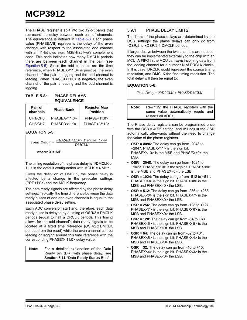
MCP3912
The PHASE register is split into two 12-bit banks thatrepresent the delay between each pair of channels.The equivalence is defined in Table 5-8. Each phasevalue (PHASEA/B) represents the delay of the evenchannel with respect to the associated odd channelwith an 11-bit plus sign, MSB-first two's complementcode. This code indicates how many DMCLK periodsthere are between each channel in the pair. (seeEquation 5-5). Since the odd channels are the timereference, when PHASEX<11:0> is positive, the evenchannel of the pair is lagging and the odd channel isleading. When PHASEX<11:0> is negative, the evenchannel of the pair is leading and the odd channel islagging.
EQUATION 5-5:
The timing resolution of the phase delay is 1/DMCLK or1 µs in the default configuration with MCLK = 4 MHz.
Given the definition of DMCLK, the phase delay isaffected by a change in the prescaler settings(PRE<1:0>) and the MCLK frequency.
The data ready signals are affected by the phase delaysettings. Typically, the time difference between the dataready pulses of odd and even channels is equal to theassociated phase delay setting.
Each ADC conversion start and, therefore, each dataready pulse is delayed by a timing of OSR/2 x DMCLKperiods (equal to half a DRCLK period). This timingallows for the odd channel’s data ready signals to belocated at a fixed time reference (OSR/2 x DMCLKperiods from the reset) while the even channel can beleading or lagging around this time reference with thecorresponding PHASEX<11:0> delay value.
5.9.1 PHASE DELAY LIMITS
The limits of the phase delays are determined by theOSR settings: the phase delays can only go from-OSR/2 to +OSR/2-1 DMCLK periods.
If larger delays between the two channels are needed,they can be implemented externally to the chip with anMCU. A FIFO in the MCU can save incoming data fromthe leading channel for a number N of DRCLK clocks.In this case, DRCLK would represent the coarse timingresolution, and DMCLK the fine timing resolution. Thetotal delay will then be equal to:
EQUATION 5-6:
The Phase delay registers can be programmed oncewith the OSR = 4096 setting, and will adjust the OSRautomatically afterwards without the need to changethe value of the phase registers.
• OSR = 4096: The delay can go from -2048 to +2047. PHASEX<11> is the sign bit. PHASEX<10> is the MSB and PHASEX<0> the LSB.
• OSR = 2048: The delay can go from -1024 to +1023. PHASEX<10> is the sign bit. PHASEX<9> is the MSB and PHASEX<0> the LSB.
• OSR = 1024: The delay can go from -512 to +511.PHASEX<9> is the sign bit. PHASEX<8> is the MSB and PHASEX<0> the LSB.
• OSR = 512: The delay can go from -256 to +255 PHASEX<8> is the sign bit. PHASEX<7> is the MSB and PHASEX<0> the LSB.
• OSR = 256: The delay can go from -128 to +127. PHASEX<7> is the sign bit. PHASEX<6> is the MSB and PHASEX<0> the LSB.
• OSR = 128: The delay can go from -64 to +63.PHASEX<6> is the sign bit. PHASEX<5> is the MSB and PHASEX<0> the LSB.
• OSR = 64: The delay can go from -32 to +31.PHASEX<5> is the sign bit. PHASEX<4> is the MSB and PHASEX<0> the LSB.
• OSR = 32: The delay can go from -16 to +15.PHASEX<4> is the sign bit. PHASEX<3> is the MSB and PHASEX<0> the LSB.
TABLE 5-8: PHASE DELAYS EQUIVALENCE
Pair of channels
Phase Bank Register Map
Position
CH1/CH0 PHASEA<11:0> PHASE<11:0>
CH3/CH2 PHASEB<11:0> PHASE<23:12>
Note: For a detailed explanation of the DataReady pin (DR) with phase delay, seeSection 5.11 “Data Ready Status Bits”.
Total DelayPHASEX<11:0> Decimal Code
DMCLK-----------------------------------------------------------------------------------=
where: X = A/B
Note: Rewriting the PHASE registers with thesame value automatically resets andrestarts all ADCs.
Total Delay = N/DRCLK + PHASE/DMCLK
DS20005348A-page 38 2014 Microchip Technology Inc.
MCP3912
5.10 Data Ready LinkThere are two modes defined with the DR_LINK bit inthe STATUSCOM register that control the data readypulses. The position of the data ready pulses varieswith respect to this mode, to the OSR<2:0> and to thePHASE register settings. Section 5.11 “Data ReadyStatus Bits” represents the behavior of the DataReady pin with the two DR_LINK configurations
• DR_LINK = 0: Data ready pulses from all enabled channels are output on the DR pin.
• DR_LINK = 1 (Recommended and Default mode): Only the data ready pulses from the most lagging ADC between all the active ADCs are present on the DR pin.
The lagging ADC data ready position depends on thePHASE register, the PRE<1:0> and the OSR<2:0>settings. In this mode, the active ADCs are linkedtogether, so their data is latched together when thelagging ADC output is ready. For power meteringapplications, DR_LINK = 1 is recommended (Defaultmode); it allows the host MCU to gather all channelssynchronously within a unique interrupt pulse, and itensures that all channels have been latched at thesame time so that no data corruption is happening.
5.11 Data Ready Status BitsIn addition to the data ready pin indicator, theMCP3912 device includes a separate data ready statusbit for each channel. Each ADC channel CHn isassociated to the corresponding DRSTATUS<n> thatcan be read at all times in the STATUSCOM register.These status bits can be used to synchronize the dataretrieval in case the DR pin is not connected (seeSection 6.8 “ADC Channels Latching andSynchronization”).
The DRSTATUS<3:0> bits are not writable; writing onthem has no effect. They have a default value of '1',which indicates that the data of the corresponding ADCis not ready. This means that the ADC output registerhas not been updated since the last reading (or sincethe last reset). The DRSTATUS bits take the '0' state,once the ADC channel register is updated (which hap-pens at a DRCLK rate). A simple read of the STATUS-COM register clears all the DRSTATUS bits to theirdefault value ('1').
In the case of DR_LINK = 1, the DRSTATUS<3:0> bitsare all updated synchronously with the most laggingchannel at the same time the DR pulse is generated. Incase of DR_LINK = 0, each DRSTATUS bit is updatedindependently and synchronously with itscorresponding channel.
5.12 Crystal Oscillator
The MCP3912 includes a Pierce-type crystal oscillatorwith very high stability and ensures very low tempcoand jitter for the clock generation. This oscillator canhandle crystal frequencies up to 20 MHz, providedproper load capacitances and quartz quality factors areused. The crystal oscillator is enabled whenCLKEXT = 0 in the CONFIG1 register.
For a proper start-up, the load capacitors of the crystalshould be connected between OSC1 and DGND andbetween OSC2 and DGND. They should also respectEquation 5-7.
EQUATION 5-7:
When CLKEXT = 1, the crystal oscillator is bypassedby a digital buffer to allow direct clock input for anexternal clock (see Figure 4-1). In this case, the OSC2pin is pulled down internally to DGND and should beconnected to DGND externally for better EMI/EMCimmunity.
TABLE 5-9: PHASE VALUES WITHMCLK = 4 MHZ, OSR = 4096, PRE<1:0> = 00
PHASEX<11:0> for the Channel Pair
CH<n/n+1>Hex
Delay(CH<n> relative
to CH<n+1>)
0 1 1 1 1 1 1 1 1 1 1 1 0x7FF + 2047 µs
0 1 1 1 1 1 1 1 1 1 1 0 0x7FE + 2046 µs
0 0 0 0 0 0 0 0 0 0 0 1 0x001 + 1 µs
0 0 0 0 0 0 0 0 0 0 0 0 0x000 0 µs
1 1 1 1 1 1 1 1 1 1 1 1 0xFFF - 1 µs
1 0 0 0 0 0 0 0 0 0 0 1 0x801 - 2047 µs
1 0 0 0 0 0 0 0 0 0 0 0 0x800 -2048 µs
RM 1.6 106 1
f C LOAD------------------------
2<
Where:
f = crystal frequency in MHz
CLOAD = load capacitance in pF including parasitics from the PCB
RM = motional resistance in ohms of the quartz
2014 Microchip Technology Inc. DS20005348A-page 39
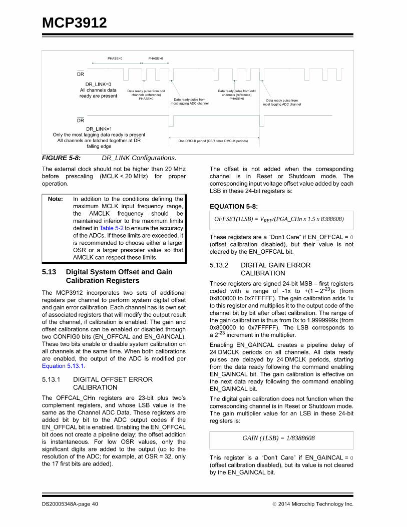
MCP3912
FIGURE 5-8: DR_LINK Configurations.
The external clock should not be higher than 20 MHzbefore prescaling (MCLK < 20 MHz) for properoperation.
5.13 Digital System Offset and Gain Calibration Registers
The MCP3912 incorporates two sets of additionalregisters per channel to perform system digital offsetand gain error calibration. Each channel has its own setof associated registers that will modify the output resultof the channel, if calibration is enabled. The gain andoffset calibrations can be enabled or disabled throughtwo CONFIG0 bits (EN_OFFCAL and EN_GAINCAL).These two bits enable or disable system calibration onall channels at the same time. When both calibrationsare enabled, the output of the ADC is modified perEquation 5.13.1.
5.13.1 DIGITAL OFFSET ERROR CALIBRATION
The OFFCAL_CHn registers are 23-bit plus two’scomplement registers, and whose LSB value is thesame as the Channel ADC Data. These registers areadded bit by bit to the ADC output codes if theEN_OFFCAL bit is enabled. Enabling the EN_OFFCALbit does not create a pipeline delay; the offset additionis instantaneous. For low OSR values, only thesignificant digits are added to the output (up to theresolution of the ADC; for example, at OSR = 32, onlythe 17 first bits are added).
The offset is not added when the correspondingchannel is in Reset or Shutdown mode. Thecorresponding input voltage offset value added by eachLSB in these 24-bit registers is:
EQUATION 5-8:
These registers are a “Don't Care” if EN_OFFCAL = 0(offset calibration disabled), but their value is notcleared by the EN_OFFCAL bit.
5.13.2 DIGITAL GAIN ERROR CALIBRATION
These registers are signed 24-bit MSB – first registerscoded with a range of -1x to +(1 – 2-23)x (from0x800000 to 0x7FFFFF). The gain calibration adds 1xto this register and multiplies it to the output code of thechannel bit by bit after offset calibration. The range ofthe gain calibration is thus from 0x to 1.9999999x (from0x800000 to 0x7FFFFF). The LSB corresponds toa 2-23 increment in the multiplier.
Enabling EN_GAINCAL creates a pipeline delay of24 DMCLK periods on all channels. All data readypulses are delayed by 24 DMCLK periods, startingfrom the data ready following the command enablingEN_GAINCAL bit. The gain calibration is effective onthe next data ready following the command enablingEN_GAINCAL bit.
The digital gain calibration does not function when thecorresponding channel is in Reset or Shutdown mode.The gain multiplier value for an LSB in these 24-bitregisters is:
This register is a “Don't Care” if EN_GAINCAL = 0(offset calibration disabled), but its value is not clearedby the EN_GAINCAL bit.
DR
One DRCLK period (OSR times DMCLK periods)
DR_LINK=1Only the most lagging data ready is present
All channels are latched together at DR falling edge
DR
DR_LINK=0All channels data ready are present
Data ready pulse from odd channels (reference)
PHASE=0
Data ready pulse from odd channels (reference)
PHASE=0
PHASE<0 PHASE>0
Data ready pulse from most lagging ADC channel
Data ready pulse from most lagging ADC channel
Note: In addition to the conditions defining themaximum MCLK input frequency range,the AMCLK frequency should bemaintained inferior to the maximum limitsdefined in Table 5-2 to ensure the accuracyof the ADCs. If these limits are exceeded, itis recommended to choose either a largerOSR or a larger prescaler value so thatAMCLK can respect these limits.
OFFSET(1LSB) = VREF/(PGA_CHn x 1.5 x 8388608)
GAIN (1LSB) = 1/8388608
DS20005348A-page 40 2014 Microchip Technology Inc.

MCP3912
The output data on each channel is kept to either 7FFFor 8000 (16-bit mode) or 7FFFFF or 800000 (24-bitmode) if the output results are out of bounds after allcalibrations are performed.
EQUATION 5-9: DIGITAL OFFSET AND GAIN ERROR CALIBRATION REGISTERS CALCULATIONS
DATA_CHn post cal– DATA_CHn pre cal– OFFCAL_CHn+ 1 GAINCAL_CHn+ =
2014 Microchip Technology Inc. DS20005348A-page 41

MCP3912
6.0 SPI SERIAL INTERFACE DESCRIPTION
6.1 Overview
The MCP3912 device includes a four-wire (CS, SCK,SDI, SDO) digital serial interface that is compatible withSPI Modes 0,0 and 1,1. Data is clocked out of theMCP3912 on the falling edge of SCK, and data isclocked into the MCP3912 on the rising edge of SCK.In these modes, the SCK clock can idle either high (1,1)or low (0,0). The digital interface is asynchronous withthe MCLK clock that controls the ADC sampling anddigital filtering. All the digital input pins are Schmitt-triggered to avoid system noise perturbations on thecommunications.
Each SPI communication starts with a CS falling edgeand stops with the CS rising edge. Each SPI communi-cation is independent. When CS is logic high, SDO is inhigh-impedance and transitions on SCK and SDI haveno effect. Changing from an SPI Mode 1,1 to an SPIMode 0,0 and vice versa is possible, and can be donewhile the CS pin is logic high. Any CS rising edge clearsthe communication and resets the SPI digital interface.
Additional control pins (RESET, DR) are also providedon separate pins for advanced communicationfeatures. The Data Ready pin (DR) outputs pulseswhen a new ADC channel data is available for reading,which can be used as an interrupt for an MCU. TheMaster Reset pin (RESET) acts like a hard reset andcan reset the part to its default power-up configuration(equivalent to a POR state).
The MCP3912 interface has a simple commandstructure. Every command is either a read commandfrom a register, or a write command to a register. TheMCP3912 device includes 32 registers defined in theTable 8-1 register map. The first byte (8-bit wide)transmitted is always the CONTROL byte that definesthe address of the register and the type of command(read or write). It is followed by the register itself, whichcan be in a 16-, 24- or 32-bit format, depending on themultiple format settings defined in the STATUSCOMregister. The MCP3912 is compatible with multipleformats that help reduce overhead in the data handlingfor most MCUs and processors available on the market(8-/16- or 32-bit MCUs) and improve MCU-codecompaction and efficiency.
The MCP3912 digital interface is capable of handlingvarious continuous read and write modes, which allowsit to perform ADC data streaming or full register mapwriting within only one communication (and thereforewith only one unique control byte). The internalregisters can be grouped together with variousconfigurations through the READ<1:0> and WRITEbits. The internal address counter of the serial interfacecan be automatically incremented, with no additionalcontrol byte needed, in order to loop through thevarious groups of registers within the register map. Thegroups are defined in Table 8-2.
The MCP3912 device also includes advanced securityfeatures to secure each communication, in order toavoid unwanted write commands being processed tochange the desired configuration and to alert the userin case of a change in the desired configuration.
Each SPI read communication can be secured througha selectable CRC-16 checksum provided on the SDOpin at the end of every communication sequence. ThisCRC-16 computation is compatible with the DMA CRChardware of the PIC24 and PIC32 MCUs, resulting inno additional overhead for the added security.
For securing the entire configuration of the device, theMCP3912 includes an 8-bit lock code (LOCK<7:0>),which blocks all write commands to the full registermap if the value of the LOCK<7:0> is not equal to adefined password (0xA5). The user can protect itsconfiguration by changing the LOCK<7:0> value to0x00 after the full programming, so that any unwantedwrite command will not result in a change to theconfiguration (because LOCK<7:0> is different than thepassword 0xA5).
An additional CRC-16 calculation is also running con-tinuously in the background to ensure the integrity ofthe full register map. All writable registers of the regis-ter map (except the MOD register) are processedthrough a CRC-16 calculation engine and give a CRC-16 checksum that depends on the configuration. Thischecksum is readable on the LOCK/CRC register andupdated at all times. If a change in this checksum hap-pens, a selectable interrupt can give a flag on the DRpin (DR pin becomes logic low) to warn the user thatthe configuration is corrupted.
6.2 Control Byte
The control byte of the MCP3912 contains two deviceAddress bits (A<6:5>), five register Address bits(A<4:0>) and a Read/Write bit (R/W). The first bytetransmitted to the MCP3912 in any communication isalways the control byte. During the control byte trans-fer, the SDO pin is always in a high-impedance state.The MCP3912 interface is device addressable(through A<6:5>) so that multiple chips can be presenton the same SPI bus with no data bus contention. Evenif they use the same CS pin, they use a provided half-duplex SPI interface with a different address identifier.This functionality enables, for example, a SerialEEPROM like 24AAXXX/24LCXXX or 24FCXXX andthe MCP3912 to share all the SPI pins and consumeless I/O pins in the application processor, since allthese Serial EEPROM circuits use A<6:5> = 00. .
FIGURE 6-1: Control Byte.
A<6> A<5> A<4> A<3> A<2> A<1> A<0> R/W
Device Address
Register Address Read/Write
DS20005348A-page 42 2014 Microchip Technology Inc.

MCP3912
The default device address bits are A<6:5> = 01 (con-tact the Microchip factory for other available deviceaddress bits). For more information, see the ProductIdentification System section. The register map isdefined in Table 8-1.
6.3 Reading from the Device
The first register read on the SDO pin is the one definedby the address (A<4:0>) given in the CONTROL byte.After this first register is fully transmitted, if the CS pinis maintained logic low, the communication continueswithout an additional control byte and the SDO pintransmits another register with the addressautomatically incremented or not, depending on theREAD<1:0> bit settings.
Four different Read mode configurations can bedefined through the READ<1:0> bits in theSTATUSCOM register for the address increment (seeSection 6.5, Continuous Communications,Looping on Register Sets and Table 8-2). The dataon SDO is clocked out of the MCP3912 on the fallingedge of SCK. The reading format for each register isdefined on Section 6.5 “ContinuousCommunications, Looping on Register Sets”.
FIGURE 6-2: Read on a Single Register with 24-bit Format (WIDTH_DATA<1:0> = 01, SPI Mode 1,1).
FIGURE 6-3: Read on a Single Register with 24-bit Format (WIDTH_DATA<1:0> = 01, SPI Mode 0,0).
READ Communication (SPI mode 1,1)
Don’t careDon’t care
A<6
>
DA
TA<2
2>
SCK
SDI
SDO
A<5
>
A<4
>
A<3
>
A<2
>
A<1
>
A<0
>
CS
DA
TA<2
1>
DA
TA<2
0>
DA
TA<1
9>
DA
TA<1
8>
DA
TA<1
7>
DA
TA<1
6>
DA
TA<1
5>
DA
TA<1
4>
DA
TA<1
3>
DA
TA<1
2>
DA
TA<1
1>
DA
TA<1
0>
DA
TA<9
>
DA
TA<8
>
DA
TA<7
>
DA
TA<6
>
DA
TA<5
>
DA
TA<4
>
DA
TA<3
>
DA
TA<2
>
DA
TA<1
>
DATA<0>Hi-Z Hi-Z
Device latches SDI on rising edge Device latches SDO on falling edge
R/W
DA
TA<2
3>
READ Communication (SPI mode 0,0)
Don’t careDon’t care
Don’t care
A<6
>
DA
TA<2
2>
SCK
SDI
SDO
A<5
>
A<4
>
A<3
>
A<2
>
A<1
>
A<0
>
R/W
CS
DATA<23>
DA
TA<2
1>
DA
TA<2
0>
DA
TA<1
9>
DA
TA<1
8>
DA
TA<1
7>
DA
TA<1
6>
DA
TA<1
5>
DA
TA<1
4>
DA
TA<1
3>
DA
TA<1
2>
DA
TA<1
1>
DA
TA<1
0>
DA
TA<9
>
DA
TA<8
>
DA
TA<7
>
DA
TA<6
>
DA
TA<5
>
DA
TA<4
>
DA
TA<3
>
DA
TA<2
>
DA
TA<1
>
DA
TA<0
>
Hi-Z Hi-Z
Device latches SDI on rising edge Device latches SDO on falling edge
2014 Microchip Technology Inc. DS20005348A-page 43

MCP3912
6.4 Writing to the Device
The first register written from the SDI pin to the deviceis the one defined by the address (A<4:0>) given in theCONTROL byte. After this first register is fullytransmitted, if the CS pin is maintained logic low, thecommunication continues without an additional controlbyte and the SDI pin transmits another register with theaddress automatically incremented or not, dependingon the WRITE bit setting.
Two different Write mode configurations for theaddress increment can be defined through the WRITEbit in the STATUSCOM register (see Section 6.5, Con-tinuous Communications, Looping on RegisterSets and Table 8-2). The SDO pin stays in a high-impedance state during a write communication. Thedata on SDI is clocked into the MCP3912 on the risingedge of SCK. The writing format for each register isdefined in Section 6.5, Continuous Communica-tions, Looping on Register Sets. A write on an unde-fined or nonwritable address, such as the ADCchannel’s register addresses, will have no effect andalso will not increment the address counter.
FIGURE 6-4: Write to a Single Register with 24-bit Format (SPI Mode 1,1).
FIGURE 6-5: Write to a Single Register with 24-bit Format (SPI Mode 0,0).
WRITE Communication (SPI mode 1,1)
Don’t care
A<6
>
SCK
SDI
SDO
A<5
>
A<4
>
A<3
>
A<2
>
A<1
>
A<0
>
CS
Hi-Z
Device latches SDI on rising edge
R/W
DA
TA<2
2>
DA
TA<2
1>
DA
TA<2
0>
DA
TA<1
9>
DA
TA<1
8>
DA
TA<1
7>
DA
TA<1
6>
DA
TA<1
5>
DA
TA<1
4>
DA
TA<1
3>
DA
TA<1
2>
DA
TA<1
1>
DA
TA<1
0>
DA
TA<9
>
DA
TA<8
>
DA
TA<7
>
DA
TA<6
>
DA
TA<5
>
DA
TA<4
>
DA
TA<3
>
DA
TA<2
>
DA
TA<1
>
DA
TA<2
3>
Don’t careDATA<0>
WRITE Communication (SPI mode 0,0)
Don’t care
A<6
>
SCK
SDI
SDO
A<5
>
A<4
>
A<3
>
A<2
>
A<1
>
A<0
>
R/W
CS
Hi-Z
Device latches SDI on rising edge
Don’t care
DA
TA<2
2>
DATA<23>
DA
TA<2
1>
DA
TA<2
0>
DA
TA<1
9>
DA
TA<1
8>
DA
TA<1
7>
DA
TA<1
6>
DA
TA<1
5>
DA
TA<1
4>
DA
TA<1
3>
DA
TA<1
2>
DA
TA<1
1>
DA
TA<1
0>
DA
TA<9
>
DA
TA<8
>
DA
TA<7
>
DA
TA<6
>
DA
TA<5
>
DA
TA<4
>
DA
TA<3
>
DA
TA<2
>
DA
TA<1
>
DA
TA<0
>
DS20005348A-page 44 2014 Microchip Technology Inc.

MCP3912
6.5 Continuous Communications, Looping on Register Sets
The MCP3912 digital interface can process communi-cations in Continuous mode without having to enter anSPI command between each read or write to a register.This feature allows the user to reduce communicationoverhead to the strict minimum, which diminishes EMIemissions and reduces switching noise in the system.
The registers can be grouped into multiple sets for con-tinuous communications. The grouping of the registersin the different sets is defined by the READ<1:0> andWRITE bits that control the internal SPI communicationaddress pointer. For a graphical representation of theregister map sets in function of the READ<1:0> andWRITE bits, please see Table 8-2.
In the case of a continuous communication, there isonly one control byte on SDI to start the communicationafter a CS pin falling edge. The part stays within thesame communication loop until the CS pin returns logic
high. The SPI internal register address pointer starts bytransmitting/receiving the address defined in the con-trol byte. After this first transmission/reception, the SPIinternal register address pointer automatically incre-ments to the next available address in the register setfor each transmission/reception. When it reaches thelast address of the set, the communication sequence isfinished. The address pointer automatically loops backto the first address of the defined set and restarts a newsequence with auto-increment (see Table 6-6). Thisinternal address pointer automatic selection allows thefollowing functionality:
• Read one ADC channel data, pairs of ADC channels or all ADC channels continuously
• Continuously read the entire register map
• Continuously read or write each separate register
• Continuously read or write all configuration registers
FIGURE 6-6: Continuous Communication Sequences.
Don’t care
Continuous READ communication (24-bit format)
Don’t care
SCK
SDI
SDO
CS
Hi-Z
8x
CONTROLBYTE
24x
ADDR ... ADDR + n
Starts read sequenceat address ADDR
Complete READ sequence
ADDR + 1
24x ... 24x 24x
ADDR ...
Complete READ sequence
ADDR + 1
24x ... 24x
ADDR + n
Continuous WRITE communication (24-bit format)
Don’t care
SCK
SDI
SDO
CS
Hi-Z
8x
CONTROLBYTE
24x
ADDR ... ADDR + n
Starts write sequenceat address ADDR
Complete WRITE sequence
ADDR + 1
24x ... 24x 24x
ADDR ...
Complete WRITE sequence
ADDR + 1
24x ... 24x
ADDR + n
ADDR
ADDR + 1
...
ADDR + n
CompleteREADsequence
Roll-over
ADDRESS SET
ADDR
ADDR + 1
...
ADDR + n
CompleteWRITEsequence
Roll-over
ADDRESS SET
2014 Microchip Technology Inc. DS20005348A-page 45

MCP3912
6.5.1 CONTINUOUS READThe STATUSCOM register contains the read communica-tion loop settings for the internal register address pointer(READ<1:0> bits). For Continuous Read modes, theaddress selection can take the following four values:
Any SDI data coming after the control byte is notconsidered during a continuous read communication. Thefollowing figures represent a typical continuous readcommunication on all four ADC channels in TYPES modewith the default settings (DR_LINK = 1, READ<1:0> = 10,WIDTH_DATA<1:0> = 01) in case of the SPI Mode 0,0(Figure 6-7) and SPI Mode 1,1 (Figure 6-8).
In SPI Mode (1,1), the SDO pin stays in the last state(LSB of previous data) after a complete reading whichalso allows seamless continuous Read mode (seeFigure 6-8).
FIGURE 6-7: Typical Continuous Read Communication (WIDTH_DATA<1:0> = 01, SPI Mode 0,0).
FIGURE 6-8: Typical Continuous Read Communication (WIDTH_DATA<1:0> = 01, SPI Mode 1,1).
TABLE 6-1: ADDRESS SELECTION IN CONTINUOUS READ
READ<1:0>Register Address Set Grouping
for Continuous Read Communications
00 Static (no incrementation)
01 Groups
10 Types (default)
11 Full Register Map
Note: For continuous reading of ADC data inSPI Mode 0,0 (see Figure 6-7), once thedata has been completely read after adata ready, the SDO pin will take the MSBvalue of the previous data at the end of thereading (falling edge of the last SCKclock). If SCK stays idle at logic low (bydefinition of Mode 0,0), the SDO pin willbe updated at the falling edge of the nextdata ready pulse (synchronously with theDR pin falling edge with an output timingof tDODR) with the new MSB of the datacorresponding to the data ready pulse.This mechanism allows the MCP3912 tocontinuously read ADC data outputsseamlessly, even in SPI Mode (0,0).
Don’t care
SCK
SDI
SDO
CS
Hi-Z
8x
0x01
24x
DATA_CH0 ... DATA_CH
Starts read sequence at address 00000
Complete READ sequence on ADC outputs channels 0 to
DATA_CH1
24x ... 24x 24x
DATA_CH0 ...DATA_CH1
24x ... 24x
DATA_CH
Don’t care
DR
DATA_CH0<23>
New data
DATA_CH0<23>
Old data
Complete READ sequence on new ADC outputs channels0 to
Don’t care
SCK
SDI
SDO
CS
Hi-Z
8x
0x01
24x
DATA_CH0 ... DATA_CH
Starts read sequence at address 00000
Complete READ sequence on ADC outputs channels 0 to
DATA_CH1
24x ... 24x 24x
DATA_CH0 ...DATA_CH1
24x ... 24x
DATA_CH
Don’t care
DR
Complete READ sequence on new ADC outputs, channels 0 to
Stays at DATA_CH <0>
DS20005348A-page 46 2014 Microchip Technology Inc.

MCP3912
6.5.2 CONTINUOUS WRITE
The STATUSCOM register contains the write loopsettings for the internal register address pointer(WRITE). For a continuous write, the address selectioncan take the following two values:
SDO is always in a high-impedance state during acontinuous write communication. Writing to anon-writable address (such as addresses 0x00 to0x07) has no effect and does not increment theaddress pointer. In this case, the user needs to stop thecommunication and restart a communication with acontrol byte pointing to a writable address (0x08 to0x1F).
6.6 Situations that Reset and Restart Active ADCs
Immediately after the following actions, the activeADCs (the ones not in Soft Reset or Shutdown modes)are reset and automatically restarted in order to provideproper operation:
1. Change in PHASE register.
2. Overwrite of the same PHASE register value.
3. Change in the OSR<2:0> settings.
4. Change in the PRE<1:0> settings.
5. Change in the CLKEXT setting.
6. Change in the VREFEXT setting.
After these temporary resets, the ADCs go back toNormal operation, with no need for an additionalcommand. Each ADC data output register is clearedduring this process. The PHASE register can be usedto serially soft reset the ADCs, without using theRESET<3:0> bits in the Configuration register, if thesame value is written in the PHASE register.
6.7 Data Ready Pin (DR)
To communicate when channel data is ready for trans-mission, the data ready signal is available on the DataReady pin (DR) at the end of a channel conversion.The Data Ready pin outputs an active-low pulse with apulse width equal to half a DMCLK clock period. After adata ready pulse falling edge has occurred, the ADCoutput data is updated within the tDODR timing and canthen be read through SPI communication.
The first data ready pulse after a Hard or a Soft Resetis located after the settling time of the sinc filter (seeTable 5-3) plus the phase delay of the correspondingchannel (see Section 5.9 “Phase Delay Block”).Each subsequent pulse is then periodic, and the periodis equal to a DRCLK clock period (see Equation 4-3and Figure 1-3). The data ready pulse is always syn-chronous with the internal DRCLK clock.
The DR pin can be used as an interrupt pin when con-nected to an MCU or DSP, which will synchronize thereadings of the ADC data outputs. When not active-low,this pin can either be in high-impedance (whenDR_HIZ = 0) or in a defined logic high state (whenDR_HIZ = 1). This is controlled through the STATUS-COM register. This allows multiple devices to share thesame Data Ready pin (with a pull-up resistor connectedbetween DR and DVDD). If only the MCP3912 device isconnected on the interrupt bus, the DR pin does notrequire a pull-up resistor, and therefore it is recom-mended to use DR_HIZ = 1 configuration for suchapplications.
The CS pin has no effect over the DR pin, which meanseven if the CS pin is logic high, the data ready pulsescoming from the active ADC channels will still beprovided; the DR pin behavior is independent from theSPI interface. While the RESET pin is logic low, the DRpin is not active. The DR pin is latched in the logic lowstate when the interrupt flag on the CRCREG is presentto signal that the desired registers configuration hasbeen corrupted (see Section 6.11 “DetectingConfiguration Change Through CRC-16 ChecksumOn Register Map and its Associated InterruptFlag”).
TABLE 6-2: ADDRESS SELECTION IN CONTINUOUS WRITE
WRITERegister Address Set Grouping for Continuous Read Communications
0 Static (no incrementation)
1 Types (default)
Note: When LOCK<7:0> is different than 0xA5,all the addresses, except 0x1F, becomenonwritable (see Section 4.13“MCP3912 Delta-Sigma Architecture”)
2014 Microchip Technology Inc. DS20005348A-page 47

MCP3912
6.8 ADC Channels Latching and Synchronization
The ADC channel’s data output registers (addresses0x00 to 0x03) have a double buffer output structure.The two sets of latches in series are triggered by thedata ready signal and an internal signal indicating thebeginning of a read communication sequence (readstart).
The first set of latches holds each ADC channel dataoutput register when the data is ready, and latches allactive outputs together when DR_LINK = 1. Thisbehavior is synchronous with the DMCLK clock.
The second set of latches ensures that when readingstarts on an ADC output, the corresponding data islatched so that no data corruption can occur within aread. This behavior is synchronous with the SCK clock.If an ADC read has started, in order to read the follow-ing ADC output, the current reading needs to be fullycompleted (all bits must be read on the SDO pin fromthe ADC output data registers).
Since the double output buffer structure is triggeredwith two events that depend on two asynchronousclocks (data ready with DMCLK and read start withSCK), implement one of the three following methods onthe MCU or processor in order to synchronize thereading of the channels:
1. Use the Data Ready pin pulses as an interrupt:once a falling edge occurs on the DR pin, the datais available for reading on the ADC outputregisters after the tDODR timing. If this timing is notrespected, data corruption can occur.
2. Use a timer clocked with MCLK as asynchronization event: since the Data Readyis synchronous with DMCLK, the user cancalculate the position of the Data Readydepending on the PHASE, the OSR<2:0> andthe PRE<1:0> settings for each channel. Again,the tDODR timing needs to be added to thiscalculation, to avoid data corruption.
3. Poll the DRSTATUS<3:0> bits in theSTATUSCOM register: this method consists ofcontinuously reading the STATUSCOM registerand waiting for the DRSTATUS bits to be equal to'0'. When this event happens, the user can start anew communication to read the desired ADCdata. In this case, no additional timing is required.
The first method is the preferred one, as it can be usedwithout adding additional MCU code space, butrequires connecting the DR pin to an I/O pin of theMCU. The last two methods require more MCU codespace and execution time, but they allow synchronizedreading of the channels without connecting the DR pin,which saves one I/O pin on the MCU.
6.9 Securing Read Communications Through CRC-16 Checksum
Since power/energy metering systems can generate orreceive large EMI/EMC interferences and largetransient spikes, it is helpful to secure SPIcommunications as much as possible to maintain dataintegrity and desired configurations during the lifetimeof the application.
The communication data on the SDO pin can besecured through the insertion of a Cyclic RedundancyCheck (CRC) checksum at the end of each continuousreading sequence. The CRC checksum oncommunications can be enabled or disabled throughthe EN_CRCCOM bit in the STATUSCOM register. TheCRC message ensures the integrity of the readsequence bits transmitted on the SDO pin, and theCRC checksum is inserted in between each readsequence (see Figure 6-9).
DS20005348A-page 48 2014 Microchip Technology Inc.

MCP3912
FIGURE 6-9: Continuous Read Sequences With and Without CRC Checksum Enabled.
The CRC checksum in the MCP3912 device uses the16-bit CRC-16 ANSI polynomial as defined in the IEEE802.3 standard: x16 + x15 + x2 + 1. This polynomial canalso be noted as 0x8005. CRC-16 detects all singleand double-bit errors, all errors with an odd number ofbits, all burst errors of length 16 or less, and most errorsfor longer bursts. This allows an excellent coverage ofthe SPI communication errors that can happen in thesystem and heavily reduces the risk of amiscommunication, even under noisy environments.
The CRC-16 format displayed on the SDO pin dependson the WIDTH_CRC bit in the STATUSCOM register(see Figure 6-10). It can be either 16-bit or 32-bitformat, to be compatible with both 16-bit and 32-bitMCUs. The CRCCOM<15:0> bits calculated by theMCP3912 device are not dependent on the format (thedevice always calculates only a 16-bit CRC checksum).If a 32-bit MCU is used in the application, it isrecommended to use 32-bit formats(WIDTH_CRC = 1) only.
FIGURE 6-10: CRC Checksum Format.
The CRC calculation computed by the MCP3912device is fully compatible with CRC hardwarecontained in the Direct Memory Access (DMA) of thePIC24 and PIC32 MCU product lines. The CRCmessage that should be considered in the PIC® deviceDMA is the concatenation of the read sequence and itsassociated checksum. When the DMA CRC hardwarecomputes this extended message, the resultedchecksum should be 0x0000. Any other result indicatesthat a miscommunication has happened and that thecurrent communication sequence should be stoppedand restarted.
Continuous READ communication without CRC checksum (EN_CRCCOM=0)
Don’t care
SCK
SDI
SDO
CS
Hi-Z
8x
CONTROLBYTE
16x/24x/32xDepending on
data format
ADDR ... ADDR + n
Starts read sequence at address ADDR
Complete READ sequence
ADDR + 1
16x/24x/32xDepending on
data format...
16x/24x/32xDepending on
data format
16x/24x/32xDepending on
data format
ADDR ...
Complete READ sequence
ADDR + 1
16x/24x/32xDepending on
data format...
16x/24x/32xDepending on
data format
ADDR + n
Don’t care
ADDR
ADDR + 1
...
ADDR + n
Complete READsequence
Roll-over
ADDRESS SET
Continuous READ communication with CRC checksum (EN_CRCCOM=1)
Don’t care
SCK
SDI
SDO
CS
Hi-Z
8x
CONTROLBYTE
16x/24x/32xDepending on
data format
ADDR ... ADDR + n
Starts read sequence at address ADDR
Complete READ sequence = Message for CRC Calculation
ADDR + 1
16x/24x/32xDepending on
data format...
16x/24x/32xDepending on
data format
16x/24x/32xDepending on
data format
ADDR ...
New Message
ADDR + 1
16x/24x/32xDepending on
data format...
16x/24x/32xDepending on
data format
ADDR + n
Don’t care
ADDR
ADDR + 1
...
ADDR + n
Complete READsequence
Roll-over
ADDRESS SET
CRC Checksum CRC Checksum
16x or 32xDepending on CRC format
16x or 32xDepending on CRC format
CRC Checksum (not part of register map)
New ChecksumChecksum
* n depends on the READ<1:0>
WIDTH_CRC = 016-bit format
CRCCOM<15:8>
CRCCOM<7:0>
15 0
WIDTH_CRC = 132-bit format
CRCCOM<15:8>
CRCCOM<7:0>
31 0
0x00 0x00
Note: The CRC will be generated only at the endof the selected address set, before therollover of the address pointer occurs (seeFigure 6-9).
2014 Microchip Technology Inc. DS20005348A-page 49
MCP3912
6.10 Locking/Unlocking Register Map Write Access
The MCP3912 digital interface includes an advancedsecurity feature that permits locking or unlocking theregister map write access. This feature prevents themiscommunications that can corrupt the desiredconfiguration of the device, especially an SPI readbecoming an SPI write because of the noisyenvironment.
The last register address of the register map(0x1F: LOCK/CRC) contains the LOCK<7:0> bits. Ifthese bits are equal to the password value (which isequal to the default value of 0xA5), the register mapwrite access is not locked. Any write can take place andthe communications are not protected.
When the LOCK<7:0> bits are different than 0xA5, theregister map write access is locked. The register map,and therefore the full device configuration, is write-protected. Any write to an address other than 0x1F willyield no result. All the register addresses, except theaddress 0x1F, become read-only. In this case, if theuser wants to change the configuration, theLOCK<7:0> bits have to be reprogrammed back to0xA5 before sending the desired write command.
The LOCK<7:0> bits are located in the last register, sothe user can program the whole register map, startingfrom 0x09 to 0x1E within one continuous writesequence, and then lock the configuration at the end ofthe sequence by writing all zeros, in the address 0x1Ffor example.
6.11 Detecting Configuration Change Through CRC-16 Checksum On Register Map and its Associated Interrupt Flag
In order to prevent internal corruption of the registerand to provide additional security on the register mapconfiguration, the MCP3912 device includes anautomatic and continuous CRC checksum calculationon the full register map configuration bits. Thiscalculation is not the same as the communication CRCchecksum described in Section 6.9 “Securing ReadCommunications Through CRC-16 Checksum”.This calculation takes the full register map as the CRCmessage and outputs a checksum on theCRCREG<15:0> bits located in the LOCK/CRCregister (address 0x1F).
Since this feature is intended for protecting theconfiguration of the device, this calculation is runcontinuously only when the register map is locked(LOCK<7:0> different than 0xA5, see Section 6.10,Locking/Unlocking Register Map Write Access). Ifthe register map is unlocked, the CRCREG<15:0> bitsare cleared and no CRC is calculated.
The calculation is fully completed in 16 DMCLK periodsand refreshed every 16 DMCLK periods continuously.The CRCREG<15:0> bits are reset when a POR or ahard reset occurs. All the bits contained in the registersfrom addresses 0x09 — 0x1F are processed by theCRC engine to give the CRCREG<15:0>. TheDRSTATUS<3:0> bits are set to '1' (default) and theCRCREG<15:0> bits are set to '0' (default) for thiscalculation engine, as they could vary during thecalculation.
An interrupt flag can be enabled through the EN_INTbit in the STATUSCOM register and provided on the DRpin when the configuration has changed without a writecommand being processed. This interrupt is a logic lowstate. This interrupt is cleared when the register map isunlocked (since the CRC calculation is not processed).
At power-up, the interrupt is not present and theregister map is unlocked. As soon as the user finisheswriting its configuration, the user needs to lock theregister map (writing 0x00 for example in the LOCKbits) to be able to use the interrupt flag. TheCRCREG<15:0> bits will be calculated for the first timein 16 DMCLK periods. This first value will then be thereference checksum value and will be latched internallyuntil a hard reset, a POR or an unlocking of the registermap happens. The CRCREG<15:0> will then becalculated continuously and checked against thereference checksum. If the CRCREG<15:0> is differentthan the reference, the interrupt sends a flag by settingthe DR pin to a logic low state until it is cleared.
DS20005348A-page 50 2014 Microchip Technology Inc.

MCP3912
NOTES:
2014 Microchip Technology Inc. DS20005348A-page 51

MCP3912
7.0 BASIC APPLICATION RECOMMENDATIONS
7.1 Typical Application Examples
The application schematic referenced in Figure 7-1 canbe used as a starting point for MCP3912applications.The most common solution is to use onechannel for voltage measurement and the rest of thechannels for current measurement. Since all currentlines are at the same potential, shunts can be used ascurrent sensors, even if they do not provide anygalvanic isolation.
Since all channels are identical in the MCP3912, anychannel can be chosen as the voltage channel (prefer-ably CH0 or CH3 since they are on the edges and canlead to a cleaner layout).
FIGURE 7-1: MCP3912 Application Example Schematic.
RG9/3912_CS
RG7/3912_SDORG6/3912_SCK
RG8/3912_SDI
GND
RA5/3912_RESET
XTAL
RD3/3912_CLKINXTAL
GNDA
GND
ADC CLOCK SELECT
10MHzX1
18pF0603C7
18pF0603C6 GND
1%1M0603
R20
10R0603R17
10R0603
R7
0.1uF0603C3
10R0603
R9
0.1uF0603C4
10R0603
R6
10R0603R8
10R
0603
R10
10R0603R12
100R0603R5
10R0603R14
GNDA
GNDA
GNDA
0.1uF0603
C5
2x3X
X
1 23 4
5 6J3
ECCP3
3.3D3.3A
GND
GND GNDA GNDAGNDA
GNDACH0-
CH0+
1%1k0603R18
1%1k0603R65
GNDA
1%1k0603R67
1%1k0603R16
0.1uF0603
C50
0.1uF0603
C47
2x3
1 23 4
5 6
J7
1x3
12
3
J20
1%1k0603
R66
1%1k0603
R64
GND GNDA GNDAGNDA
GNDACH1+
CH1-
1%1k0603R69
1%1k0603R71
GNDA
1%1k0603R73
1%1k0603R68
0.1uF0603
C52
0.1uF0603
C51
2x3
1 23 4
5 6
J21
1x3
12
3
J22
1%1k0603
R72
1%1k0603
R70
GND GNDA GNDAGNDA
GNDACH2-
CH2+
1%1k0603R75
1%1k0603R77
GNDA
1%1k0603R79
1%1k0603R74
0.1uF0603
C54
0.1uF0603
C53
2x3
1 23 4
5 6
J23
1x3
12
3
J24
1%1k0603
R78
1%1k0603
R76
GND GNDA GNDAGNDA
GNDACH3+
CH3-
1%1k0603R81
1%1k0603R83
GNDA
1%1k0603R85
1%1k0603R80
0.1uF0603
C56
0.1uF0603
C55
2x3
1 23 4
5 6
J25
1x3
12
3
J26
1%1k0603
R84
1%1k0603
R82
RA14/3912_DR
NC 10
CH2-7
REFIN+14
CH2+6
CH3-8
CH3+9
REFIN-15
NC
CH2-
REFIN+
CH2+
CH3-CH3+
REFIN-
DGND 20
DR 18
OSC1/CLKI 21OSC2 22
CS 23SCK 24SDO 25SDI 26RESET 27
DGND 17
DVDD 28AVDD1
AGND16
CH0+2
CH0-3
CH1-4
CH1+5
NC 11NC 12NC 13NC 19
MCP3912U5
ADC
CH0+CH0-
CH1-CH1+
CH2+CH2-
CH3-CH3+
DS20005348A-page 52 2014 Microchip Technology Inc.

MCP3912
7.2 Power Supply Design and Bypassing
The MCP3912 device was designed to measure posi-tive and negative voltages that might be generated bya current sensing device. This current sensing device,with a common mode voltage close to 0V, is referred toas AGND, which is a shunt or current transformer (CT)with burden resistors attached to ground. The high per-formance and good flexibility that characterize thisADC enables them to be used in other applications, aslong as the absolute voltage on each pin, referred toAGND, stays in the -1V to +1V interval.
In any system, the analog ICs (such as references oroperational amplifiers) are always connected to theanalog ground plane. The MCP3912 should also beconsidered as a sensitive analog component, and con-nected to the analog ground plane. The ADC featurestwo pairs of pins: AGND, AVDD, DGND and DVDD. Forbest performance, it is recommended to keep the twopairs connected to two different networks (Figure 7-2).This way, the design will feature two ground traces andtwo power supplies (Figure 7-3).
This means the analog circuitry (including MCP3912)and the digital circuitry (MCU) should have separatepower supplies and return paths to the external groundreference, as described in Figure 7-2. An example of atypical power supply circuit, with different lines for ana-log and digital power, is shown in Figure 7-3. A possiblesplit example is shown in Figure 7-4, where the groundstar connection can be done at the bottom of the devicewith the exposed pad. The split here between analogand digital can be done under the device, and AVDDand DVDD can be connected together with lines comingunder the ground plane.
Another possibility, sometimes easier to implement interms of PCB layout, is to consider the MCP3912 as ananalog component and, therefore, connect both AVDDand DVDD together, and AGND and DGND together witha star connection. In this scheme, the decouplingcapacitors may be larger due to the ripple on the digitalpower supply (caused by the digital filters and the SPIinterface of the MCP3912) now causing glitches on theanalog power supply.
FIGURE 7-2: All Analog and Digital Return Paths Need to Stay Separate with Proper Bypass Capacitors.
FIGURE 7-3: Power Supply with Separate Lines for Analog and Digital Sections. Note the "Net Tie" Object NT2 that Represents the Start Ground Connection.
VA VD
MCU
“Star” Point
IA
ID
IDIA
AVDD DVDD
AGND DGND
D-= A-=
0.1 μF
MCP39XX
0.1 μF C
2014 Microchip Technology Inc. DS20005348A-page 53

MCP3912
FIGURE 7-4: Separation of Analog and Digital Circuits on Layout.
Figure 7-5 shows a more detailed example with a directconnection to a high-voltage line (e.g., a two-wire 120Vor 220V system). A current-sensing shunt is used forcurrent measurement on the high side/line side thatalso supplies the ground for the system. This isnecessary as the shunt is directly connected to thechannel input pins of the MCP3912. To reducesensitivity to external influences such as EMI, thesetwo wires should form a twisted pair, as noted inFigure 7-5. The power supply and MCU are separatedon the right side of the PCB, surrounded by the digitalground plane. The MCP3912 is kept on the left side,surrounded by the analog ground plane. There are twoseparate power supplies going to the digital section ofthe system and the analog section, including theMCP3912. With this placement, there are two separatecurrent supply paths and current return paths, IA and ID.
FIGURE 7-5: Connection Diagram.
The ferrite bead between the digital and analog groundplanes helps keep high-frequency noise from enteringthe device. This ferrite bead is recommended to be low
resistance; most often it is a THT component. Ferritebeads are typically placed on the shunt inputs and intothe power supply circuit for additional protection.
7.3 SPI Interface Digital Crosstalk
The MCP3912 incorporates a high-speed 20 MHz SPIdigital interface. This interface can induce a crosstalk,especially with the outer channels (CH0, for example),if it is running at its full speed without any precautions.The crosstalk is caused by the switching noise createdby the digital SPI signals (also called ground bouncing).This crosstalk would negatively impact the SNR in thiscase. The noise is attenuated if a proper separationbetween the analog and digital power supplies is put inplace (see Section 7.2 “Power Supply Design andBypassing”).
In order to further remove the influence of the SPIcommunication on measurement accuracy, it isrecommended to add series resistors on the SPI linesto reduce the current spikes caused by the digitalswitching noise (see Figure 7-5 where these resistorshave been implemented). The resistors also help tokeep the level of electromagnetic emissions low.
The measurement graphs provided in this MCP3912data sheet have been performed with 100 seriesresistors connected on each SPI I/O pin. Measurementaccuracy disturbances have not been observed even atthe full speed of 20 MHz interfacing.
The crosstalk performance is dependent on thepackage choice due to the difference in the pinarrangement (dual in-line or quad), and is improved inthe QFN-28 package.
7.4 Sampling Speed and Bandwidth
If ADC power consumption is not a concern in thedesign, the boost settings can be increased for bestperformance so that the OSR is always kept at themaximum settings to improve the SINAD performance(see Table 7-1). If the MCU cannot generate a clockfast enough, it is possible to tap the OSC1/OSC2 pinsof the MCP3912 crystal oscillator directly to the crystalof the microcontroller. When the sampling frequency isenlarged, the phase resolution is improved, and withthe OSR increased, the phase compensation rangecan be kept in the same range as the default settings.
MCU
Power SupplyCircuitry
LINE
NEUTRAL
SHUNT
Twisted Pair
IA
ID
ID
IA
“Star” Point
VAVD
Analog Ground Plane Digital Ground Plane
MCP3912
TABLE 7-1: SAMPLING SPEED VS. MCLK AND OSR, ADC PRESCALE 1:1
MCLK (MHz)
Boost<1:0> OSRSampling
Speed (ksps)
16 11 1024 3.91
14 11 1024 3.42
12 11 1024 2.93
DS20005348A-page 54 2014 Microchip Technology Inc.

MCP3912
7.5 Differential Inputs Anti-Aliasing Filter
Due to the nature of the ADCs used in the MCP3912(oversampling converters), each differential input of theADC channels requires an anti-aliasing filter so that theoversampling frequency (DMCLK) is largely attenuatedand does not generate any disturbances on the ADCaccuracy. This anti-aliasing filter also needs to have again close to one in the signal bandwidth of interest.
Typically for 50/60 Hz measurement and default set-tings (DMCLK = 1 MHz), a simple RC filter with 1 kand 100 nF can be used. The anti-aliasing filter usedfor the measurement graphs is a first-order RC filterwith 1 k and 15 nF. The typical schematic for connect-ing a current transformer to the ADC is shown inFigure 7-6. If wires are involved, twisting them is alsorecommended.
FIGURE 7-6: First-Order Anti-Aliasing Filter for CT-Based Designs.
The di/dt current sensors, such as Rogowski coils, canbe an alternative to current transformers. Since thesesensing elements are highly sensitive to high-frequency electromagnetic fields, using a second orderanti-aliasing filter is recommended to increase theattenuation of potential perturbing RF signals.
FIGURE 7-7: Second-Order Anti-Aliasing Filter for Rogowski Coil-Based Designs.
10 10 1024 2.44
8 10 512 3.91
6 01 512 2.93
4 01 256 3.91
TABLE 7-1: SAMPLING SPEED VS. MCLK AND OSR, ADC PRESCALE 1:1
MCLK (MHz)
Boost<1:0> OSRSampling
Speed (ksps)
2014 Microchip Technology Inc. DS20005348A-page 55

MCP3912
The MCP3912 is highly recommended in applicationsusing di/dt as current sensors because of the extremelylow noise floor at low frequencies. In such applications,a low-pass filter (LPF) with a cut-off frequency muchlower than the signal frequency (50-60 Hz for metering)is used to compensate for the 90 degree shift and forthe 20 db/decade attenuation induced by the di/dt sen-sor. Because of this filter, the SNR will be decreased,since the signal will attenuate by a few orders of mag-nitude while the low-frequency noise will not be attenu-ated. Usually, a high-order high-pass filter (HPF) isused to attenuate the low-frequency noise in order toprevent a dramatic degradation of the SNR, which canbe very important in other parts. A high-order filter willalso consume a significant portion of the computationpower of the MCU. When using the MCP3912, such ahigh-order HPF is not required since this part has a lownoise floor at low frequencies. A first-order HPF isenough to achieve very good accuracy.
7.6 Energy Measurement Error Considerations
The measurement error is a typical representation ofthe nonlinearity of a pair of ADCs (see Section 4.0“Terminology And Formulas” for the definition ofmeasurement error). The measurement error isdependent on the THD and on the noise floor of theADCs.
Improving the measurement error specification on theMCP3912 can be realized by increasing the OSR (toget a better SINAD and THD performance) and, tosome extent, the BOOST settings (if the bandwidth ofthe measurements is too limited by the bandwidth ofthe amplifiers in the sigma-delta ADCs). In most of theenergy metering AC applications, high-pass filters areused to cancel the offset on each ADC channel (currentand voltage channels), and therefore a single-pointcalibration is necessary to calibrate the system foractive energy measurement. This calibration is asystem gain calibration, and the user can utilize theEN_GAINCAL bit and the GAINCAL_CHn registers toperform this digital calibration. After such calibration,typical measurement error curves like Figure 2-7 canbe generated by sweeping the current channelamplitude and measuring the energy at the outputs (theenergy calculations here are being realized off-chip).The error is measured using a gain of 1x, as it iscommonly used in most CT-based applications.
At low signal amplitude values (typically 1000:1dynamic range and higher), the crosstalk betweenchannels, mainly caused by the PCB, becomes asignificant part of the perturbation as the measurementerror increases. The 1-point measurement error curvesin Figure 2-5 have been performed with a full-scalesine wave on all the inputs that are not measured,which means that these channels induce a maximumamount of crosstalk on the measurement error curve.In order to avoid such behavior, a 2-point calibrationcan be put in place in the calculation section.
This 2-point calibration can be a simple linearinterpolation between two calibration points (one athigh amplitudes, one at low amplitudes at each end ofthe dynamic range) and helps to significantly lower theeffect of crosstalk between channels. A 2-pointcalibration is very effective in maintaining themeasurement error close to zero on the whole dynamicrange, since the nonlinearity and distortion of theMCP3912 is very low. Figure 2-6 shows themeasurement error curves obtained with the sameADC data taken for Figure 2-5, but where a 2-pointcalibration has been applied. The difference issignificant only at the low end of the dynamic range,where all the perturbing factors are a bigger part of theADC output signals. These curves show extremely tightmeasurement error across the full dynamic range(here, typically 10,000:1), which is required inhigh-accuracy class meters.
DS20005348A-page 56 2014 Microchip Technology Inc.

MCP3912
NOTES:
2014 Microchip Technology Inc. DS20005348A-page 57

MCP3912
8.0 MCP3912 INTERNAL REGISTERS
The addresses associated with the internal registersare listed in Table 8-1. This section also describes theregisters in detail. All registers are 24-bit long registers,which can be addressed and read separately.
The format of the data registers (0x00 to 0x03) can bechanged with WIDTH_DATA<1:0> bits in theSTATUSCOM register. The READ<1:0> and WRITEbits define the groups and types of registers forcontinuous read/write communication or looping onaddress sets, as shown in Table 8-2.
TABLE 8-1: MCP3912 REGISTER MAP
Address Name Bits R/W Description
0x00 CHANNEL0 24 R Channel 0 ADC Data <23:0>, MSB first
0x01 CHANNEL1 24 R Channel 1 ADC Data <23:0>, MSB first
0x02 CHANNEL2 24 R Channel 2 ADC Data <23:0>, MSB first
0x03 CHANNEL3 24 R Channel 3 ADC Data <23:0>, MSB first
0x04 Unused 24 U Unused
0x05 Unused 24 U Unused
0x06 Unused 24 U Unused
0x07 Unused 24 U Unused
0x08 MOD 24 R/W Delta-Sigma Modulators Output Value
0x09 Unused 24 R/W Unused
0x0A PHASE 24 R/W Phase Delay Configuration Register - Channel pairs 0/1 and 2/3
0x0B GAIN 24 R/W Gain Configuration Register
0x0C STATUSCOM 24 R/W Status and Communication Register
0x0D CONFIG0 24 R/W Configuration Register
0x0E CONFIG1 24 R/W Configuration Register
0x0F OFFCAL_CH0 24 R/W Offset Correction Register - Channel 0
0x10 GAINCAL_CH0 24 R/W Gain Correction Register - Channel 0
0x11 OFFCAL_CH1 24 R/W Offset Correction Register - Channel 1
0x12 GAINCAL_CH1 24 R/W Gain Correction Register - Channel 1
0x13 OFFCAL_CH2 24 R/W Offset Correction Register - Channel 2
0x14 GAINCAL_CH2 24 R/W Gain Correction Register - Channel 2
0x15 OFFCAL_CH3 24 R/W Offset Correction Register - Channel 3
0x16 GAINCAL_CH3 24 R/W Gain Correction Register - Channel 3
0x17 Unused 24 U Unused
0x18 Unused 24 U Unused
0x19 Unused 24 U Unused
0x1A Unused 24 U Unused
0x1B Unused 24 U Unused
0x1C Unused 24 U Unused
0x1D Unused 24 U Unused
0x1E Unused 24 U Unused
0x1F LOCK/CRC 24 R/W Security Register (Password and CRC-16 on Register Map)
DS20005348A-page 58 2014 Microchip Technology Inc.
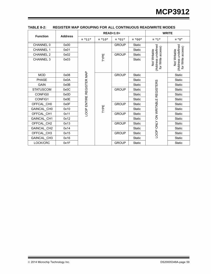
MCP3912
TABLE 8-2: REGISTER MAP GROUPING FOR ALL CONTINUOUS READ/WRITE MODES
Function AddressREAD<1:0> WRITE
= “11” = “10” = “01” = “00” = “1” = “0”
CHANNEL 0 0x00
LOO
P E
NT
IRE
RE
GIS
TE
R M
AP
TY
PE
GROUP Static
Not
Wri
tab
le
(Add
ress
un
defin
ed
for
Writ
e a
cce
ss)
Not
Wri
tab
le
(Add
ress
un
defin
ed
for
Writ
e a
cce
ss)
CHANNEL 1 0x01 Static
CHANNEL 2 0x02 GROUP Static
CHANNEL 3 0x03 Static
MOD 0x08
TY
PE
GROUP Static
LOO
P O
NLY
ON
WR
ITA
BLE
RE
GIS
TE
RS
Static
PHASE 0x0A Static Static
GAIN 0x0B Static Static
STATUSCOM 0x0C GROUP Static Static
CONFIG0 0x0D Static Static
CONFIG1 0x0E Static Static
OFFCAL_CH0 0x0F GROUP Static Static
GAINCAL_CH0 0x10 Static Static
OFFCAL_CH1 0x11 GROUP Static Static
GAINCAL_CH1 0x12 Static Static
OFFCAL_CH2 0x13 GROUP Static Static
GAINCAL_CH2 0x14 Static Static
OFFCAL_CH3 0x15 GROUP Static Static
GAINCAL_CH3 0x16 Static Static
LOCK/CRC 0x1F GROUP Static Static
2014 Microchip Technology Inc. DS20005348A-page 59

MCP3912
8.1 CHANNEL Registers - ADC Channel Data Output Registers
The ADC Channel Data Output registers alwayscontain the most recent A/D conversion data for eachchannel. These registers are read-only. They can beaccessed independently or linked together (withREAD<1:0> bits). These registers are latched when anADC read communication occurs. When a data readyevent occurs during a read communication, the mostcurrent ADC data is also latched to avoid datacorruption issues. These registers are updated andlatched together if DR_LINK = 1 synchronously withthe data ready pulse (toggling on the most laggingADC channel data ready event).
Name Bits Address Cof.
CHANNEL0 24 0x00 R
CHANNEL1 24 0x01 R
CHANNEL2 24 0x02 R
CHANNEL3 24 0x03 R
REGISTER 8-1: MCP3912 CHANNEL REGISTERS
R-0 R-0 R-0 R-0 R-0 R-0 R-0 R-0
DATA_CHn<23> (MSB)
DATA_CHn<22>
DATA_CHn<21>
DATA_CHn<20>
DATA_CHn<19>
DATA_CHn<18>
DATA_CHn<17>
DATA_CHn<16>
bit 23 bit 16
R-0 R-0 R-0 R-0 R-0 R-0 R-0 R-0
DATA_CHn<15>
DATA_CHn<14>
DATA_CHn<13>
DATA_CHn<12>
DATA_CHn<11>
DATA_CHn<10>
DATA_CHn<9>
DATA_CHn<8>
bit 15 bit 8
R-0 R-0 R-0 R-0 R-0 R-0 R-0 R-0
DATA_CHn<7>
DATA_CHn<6>
DATA_CHn<5>
DATA_CHn<4>
DATA_CHn<3>
DATA_CHn<2>
DATA_CHn<1>
DATA_CHn<0>
bit 7 bit 0
Legend:
R = Readable bit W = Writable bit U = Unimplemented bit, read as ‘0’
-n = Value at POR ‘1’ = Bit is set ‘0’ = Bit is cleared x = Bit is unknown
bit 23-0 DATA_CHn: Output code from ADC Channel n. This data is post-calibration if the EN_OFFCAL orEN_GAINCAL bits are enabled. This data can be formatted in 16-/24-/32-bit modes, depending on theWIDTH_DATA<1:0> settings. (see Section 5.5 “ADC Output Coding”)
DS20005348A-page 60 2014 Microchip Technology Inc.
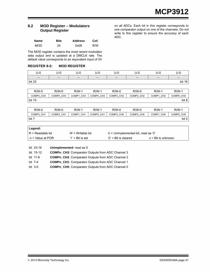
MCP3912
8.2 MOD Register – Modulators Output Register
The MOD register contains the most recent modulatordata output and is updated at a DMCLK rate. Thedefault value corresponds to an equivalent input of 0V
on all ADCs. Each bit in this register corresponds toone comparator output on one of the channels. Do notwrite to this register to ensure the accuracy of eachADC.
.
Name Bits Address Cof.
MOD 24 0x08 R/W
REGISTER 8-2: MOD REGISTER
U-0 U-0 U-0 U-0 U-0 U-0 U-0 U-0
— — — — — — — —
bit 23 bit 16
R/W-0 R/W-0 R/W-1 R/W-1 R/W-0 R/W-0 R/W-1 R/W-1
COMP3_CH3 COMP2_CH3 COMP1_CH3 COMP0_CH3 COMP3_CH2 COMP2_CH2 COMP1_CH2 COMP0_CH2
bit 15 bit 8
R/W-0 R/W-0 R/W-1 R/W-1 R/W-0 R/W-0 R/W-1 R/W-1
COMP3_CH1 COMP2_CH1 COMP1_CH1 COMP0_CH1 COMP3_CH0 COMP2_CH0 COMP1_CH0 COMP0_CH0
bit 7 bit 0
Legend:
R = Readable bit W = Writable bit U = Unimplemented bit, read as ‘0’
-n = Value at POR ‘1’ = Bit is set ‘0’ = Bit is cleared x = Bit is unknown
bit 23-16 Unimplemented: read as 0
bit 15-12 COMPn_CH3: Comparator Outputs from ADC Channel 3
bit 11-8 COMPn_CH2: Comparator Outputs from ADC Channel 2
bit 7-4 COMPn_CH1: Comparator Outputs from ADC Channel 1
bit 3-0 COMPn_CH0: Comparator Outputs from ADC Channel 0
2014 Microchip Technology Inc. DS20005348A-page 61

MCP3912
8.3 PHASE Register – Phase Configuration Register for Channel Pairs 2/3 and 0/1
Any write to this register automatically resets andrestarts all active ADCs.
Name Bits Address Cof.
PHASE 24 0x0A R/W
REGISTER 8-3: PHASE REGISTER
R/W-0 R/W-0 R/W-0 R/W-0 R/W-0 R/W-0 R/W-0 R/W-0
PHASEB<11> PHASEB<10> PHASEB<9> PHASEB<8> PHASEB<7> PHASEB<6> PHASEB<5> PHASEB<4>
bit 23 bit 16
R/W-0 R/W-0 R/W-0 R/W-0 R/W-0 R/W-0 R/W-0 R/W-0
PHASEB<3> PHASEB<2> PHASEB<1> PHASEB<0> PHASEA<11> PHASEA<10> PHASEA<9> PHASEA<8>
bit 15 bit 8
R/W-0 R/W-0 R/W-0 R/W-0 R/W-0 R/W-0 R/W-0 R/W-0
PHASEA<7> PHASEA<6> PHASEA<5> PHASEA<4> PHASEA<3> PHASEA<2> PHASEA<1> PHASEA<0>
bit 7 bit 0
Legend:
R = Readable bit W = Writable bit U = Unimplemented bit, read as ‘0’
-n = Value at POR ‘1’ = Bit is set ‘0’ = Bit is cleared x = Bit is unknown
bit 23-12 PHASEB<11:0> Phase delay between channels CH2 and CH3 (reference). Delay = PHASEB<11:0> decimal code/DMCLK
bit 11-0 PHASEA<11:0> Phase delay between channels CH0 and CH1(reference). Delay = PHASEA<11:0> decimal code/DMCLK
DS20005348A-page 62 2014 Microchip Technology Inc.
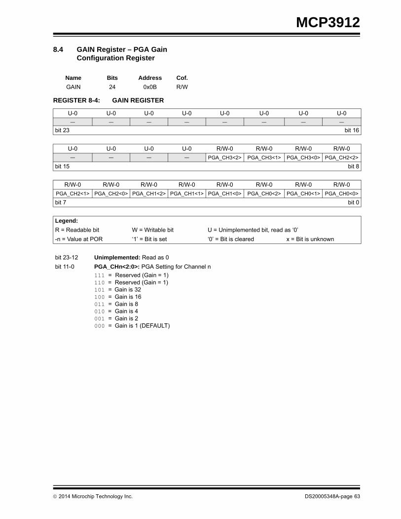
MCP3912
8.4 GAIN Register – PGA Gain Configuration Register
Name Bits Address Cof.
GAIN 24 0x0B R/W
REGISTER 8-4: GAIN REGISTER
U-0 U-0 U-0 U-0 U-0 U-0 U-0 U-0
— — — — — — — —
bit 23 bit 16
U-0 U-0 U-0 U-0 R/W-0 R/W-0 R/W-0 R/W-0
— — — — PGA_CH3<2> PGA_CH3<1> PGA_CH3<0> PGA_CH2<2>
bit 15 bit 8
R/W-0 R/W-0 R/W-0 R/W-0 R/W-0 R/W-0 R/W-0 R/W-0
PGA_CH2<1> PGA_CH2<0> PGA_CH1<2> PGA_CH1<1> PGA_CH1<0> PGA_CH0<2> PGA_CH0<1> PGA_CH0<0>
bit 7 bit 0
Legend:
R = Readable bit W = Writable bit U = Unimplemented bit, read as ‘0’
-n = Value at POR ‘1’ = Bit is set ‘0’ = Bit is cleared x = Bit is unknown
bit 23-12 Unimplemented: Read as 0
bit 11-0 PGA_CHn<2:0>: PGA Setting for Channel n
111 = Reserved (Gain = 1)110 = Reserved (Gain = 1)101 = Gain is 32100 = Gain is 16011 = Gain is 8010 = Gain is 4001 = Gain is 2000 = Gain is 1 (DEFAULT)
2014 Microchip Technology Inc. DS20005348A-page 63

MCP3912
8.5 STATUSCOM Register – Status and Communication Register
Name Bits Address Cof.
STATUSCOM 24 0x0C R/W
REGISTER 8-5: STATUSCOM REGISTER
R/W-1 R/W-0 R/W-1 R/W-0 R/W-1 R/W-0 R/W-0 R/W-1
READ<1> READ<0> WRITE DR_HIZ DR_LINK WIDTH_ CRC WIDTH_ DATA<1> WIDTH_ DATA<0>
bit 23 bit 16
R/W-0 R/W-0 R/W-0 R/W-0 U-0 U-0 U-0 U-0
EN_CRCCOM EN_INT Reserved Reserved — — — —
bit 15 bit 8
U-0 U-0 U-0 U-0 R-1 R-1 R-1 R-1
— — — — DRSTATUS<3> DRSTATUS<2> DRSTATUS<1> DRSTATUS<0>
bit 7 bit 0
Legend:
R = Readable bit W = Writable bit U = Unimplemented bit, read as ‘0’
-n = Value at POR ‘1’ = Bit is set ‘0’ = Bit is cleared x = Bit is unknown
bit 23-22 READ<1:0>: Address counter increment setting for Read Communication
11 = Address counter auto-increments, and loops on the entire register map10 = Address counter auto-increments, and loops on register TYPES (DEFAULT)01 = Address counter auto-increments, and loops on register GROUPS00 = Address is not incremented, and continually reads the same single-register address
bit 21 WRITE: Address counter increment setting for Write Communication
1 = Address counter auto-increments and loops on writable part of the register map (DEFAULT)0 = Address is not incremented, and continually writes to the same single register address
bit 20 DR_HIZ: Data Ready Pin Inactive State Control
1 = The DR pin state is a logic high when data is NOT ready0 = The DR pin state is high-impedance when data is NOT ready (DEFAULT)
bit 19 DR_LINK Data Ready Link Control
1 = Data Ready link enabled. Only one pulse is generated on the DR pin for all ADC channels,corresponding to the data ready pulse of the most lagging ADC. (DEFAULT)
0 = Data Ready link disabled. Each ADC produces its own data ready pulse on the DR pin.
bit 18 WIDTH_CRC Format for CRC-16 on communications
1 = 32-bit (CRC-16 code is followed by zeros). This coding is compatible with CRC implementation inmost 32-bit MCUs (including PIC32 MCUs).
0 = 16 bit (default)
bit 17-16 WIDTH_DATA<1:0>: ADC Data Format Settings for all ADCs (see Section 5.5 “ADC Output Coding”)
11 = 32-bit with sign extension10 = 32-bit with zeros padding01 = 24-bit (default)00 = 16-bit (with rounding)
bit 15 EN_CRCCOM: Enable CRC CRC-16 Checksum on Serial communications
1 = CRC-16 Checksum is provided at the end of each communication sequence (therefore eachcommunication is longer). The CRC-16 Message is the complete communication sequence (seesection Section 6.9 “Securing Read Communications Through CRC-16 Checksum” for moredetails).
0 = Disabled (Default)
DS20005348A-page 64 2014 Microchip Technology Inc.
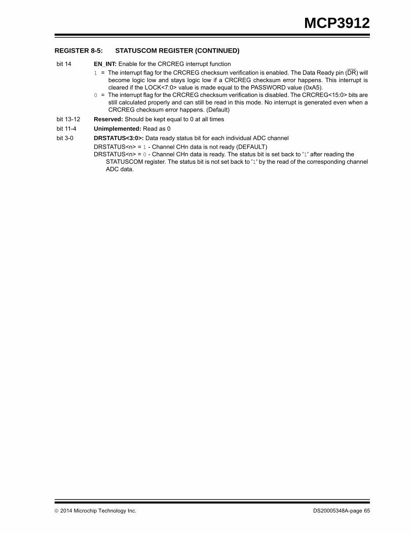
MCP3912
bit 14 EN_INT: Enable for the CRCREG interrupt function
1 = The interrupt flag for the CRCREG checksum verification is enabled. The Data Ready pin (DR) willbecome logic low and stays logic low if a CRCREG checksum error happens. This interrupt iscleared if the LOCK<7:0> value is made equal to the PASSWORD value (0xA5).
0 = The interrupt flag for the CRCREG checksum verification is disabled. The CRCREG<15:0> bits arestill calculated properly and can still be read in this mode. No interrupt is generated even when aCRCREG checksum error happens. (Default)
bit 13-12 Reserved: Should be kept equal to 0 at all times
bit 11-4 Unimplemented: Read as 0
bit 3-0 DRSTATUS<3:0>: Data ready status bit for each individual ADC channel
DRSTATUS<n> = 1 - Channel CHn data is not ready (DEFAULT)DRSTATUS<n> = 0 - Channel CHn data is ready. The status bit is set back to '1' after reading the
STATUSCOM register. The status bit is not set back to '1' by the read of the corresponding channelADC data.
REGISTER 8-5: STATUSCOM REGISTER (CONTINUED)
2014 Microchip Technology Inc. DS20005348A-page 65

MCP3912
8.6 CONFIG0 Register – Configuration Register 0
Name Bits Address Cof.
CONFIG0 24 0x0D R/W
REGISTER 8-6: CONFIG0 REGISTER
R/W-0 R/W-0 R/W-1 R/W-1 R/W-1 R/W-0 R/W-0 R/W-0
EN_OFFCAL EN_GAINCAL DITHER<1> DITHER<0> BOOST<1> BOOST<0> PRE<1> PRE<0>
bit 23 bit 16
R/W-0 R/W-1 R/W-1 U-0 U-0 U-0 U-0 U-0
OSR<2> OSR<1> OSR<0> — — — — —
bit 15 bit 8
R/W-0 R/W-1 R/W-0 R/W-1 R/W-0 R/W-0 R/W-0 R/W-0
VREFCAL<7> VREFCAL<6> VREFCAL<5> VREFCAL<4> VREFCAL<3> VREFCAL<2> VREFCAL<1> VREFCAL<0>
bit 7 bit 0
Legend:
R = Readable bit W = Writable bit U = Unimplemented bit, read as ‘0’
-n = Value at POR ‘1’ = Bit is set ‘0’ = Bit is cleared x = Bit is unknown
bit 23 EN_OFFCAL: Enables the 24-bit digital offset error calibration on all channels
1 = Enabled. This mode does not add any group delay to the ADC data.0 = Disabled (DEFAULT)
bit 22 EN_GAINCAL: Enables or disables the 24-bit digital gain error calibration on all channels
1 = Enabled. This mode adds a group delay on all channels of 24 DMCLK periods. All data readypulses are delayed by 24 DMCLK clock periods, compared to the mode with EN_GAINCAL = 0.
0 = Disabled (DEFAULT)
bit 21-20 DITHER<1:0>: Control for dithering circuit for idle tone’s cancellation and improved THD on all channels
11 = Dithering ON, Strength = Maximum (DEFAULT)10 = Dithering ON, Strength = Medium01 = Dithering ON, Strength = Minimum00 = Dithering turned OFF
bit 19-18 BOOST<1:0>: Bias Current Selection for all ADCs (impacts achievable maximum sampling speed, seeTable 5-2)
11 = All channels have current x 210 = All channels have current x 1 (Default)01 = All channels have current x 0.6600 = All channels have current x 0.5
bit 17-16 PRE<1:0> Analog Master Clock (AMCLK) Prescaler Value
11 = AMCLK = MCLK/810 = AMCLK = MCLK/401 = AMCLK = MCLK/200 = AMCLK = MCLK (Default)
DS20005348A-page 66 2014 Microchip Technology Inc.
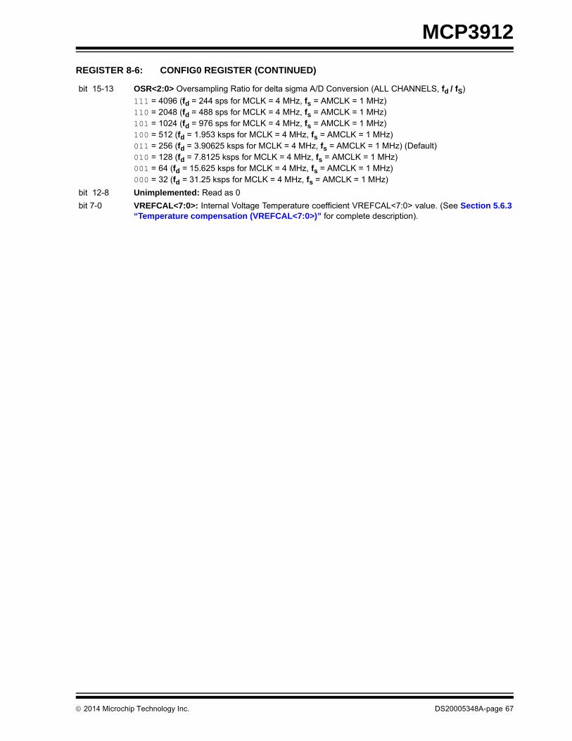
MCP3912
bit 15-13 OSR<2:0> Oversampling Ratio for delta sigma A/D Conversion (ALL CHANNELS, fd / fS)
111 = 4096 (fd = 244 sps for MCLK = 4 MHz, fs = AMCLK = 1 MHz)110 = 2048 (fd = 488 sps for MCLK = 4 MHz, fs = AMCLK = 1 MHz)101 = 1024 (fd = 976 sps for MCLK = 4 MHz, fs = AMCLK = 1 MHz)100 = 512 (fd = 1.953 ksps for MCLK = 4 MHz, fs = AMCLK = 1 MHz)011 = 256 (fd = 3.90625 ksps for MCLK = 4 MHz, fs = AMCLK = 1 MHz) (Default)010 = 128 (fd = 7.8125 ksps for MCLK = 4 MHz, fs = AMCLK = 1 MHz)001 = 64 (fd = 15.625 ksps for MCLK = 4 MHz, fs = AMCLK = 1 MHz)000 = 32 (fd = 31.25 ksps for MCLK = 4 MHz, fs = AMCLK = 1 MHz)
bit 12-8 Unimplemented: Read as 0
bit 7-0 VREFCAL<7:0>: Internal Voltage Temperature coefficient VREFCAL<7:0> value. (See Section 5.6.3“Temperature compensation (VREFCAL<7:0>)” for complete description).
REGISTER 8-6: CONFIG0 REGISTER (CONTINUED)
2014 Microchip Technology Inc. DS20005348A-page 67

MCP3912
8.7 CONFIG1 Register – Configuration Register 1
Name Bits Address Cof.
CONFIG1 24 0x0E R/W
REGISTER 8-7: CONFIG1 REGISTER
U-0 U-0 U-0 U-0 R/W-0 R/W-0 R/W-0 R/W-0
— — — — RESET<3> RESET<2> RESET<1> RESET<0>
bit 23 bit 16
U-0 U-0 U-0 U-0 R/W-0 R/W-0 R/W-0 R/W-0
— — — — SHUTDOWN<3> SHUTDOWN<2> SHUTDOWN<1> SHUTDOWN<0>
bit 15 bit 8
R/W-0 R/W-1 U-0 U-0 U-0 U-0 U-0 U-0
VREFEXT CLKEXT — — — — — —
bit 7 bit 0
Legend:
R = Readable bit W = Writable bit U = Unimplemented bit, read as ‘0’
-n = Value at POR ‘1’ = Bit is set ‘0’ = Bit is cleared x = Bit is unknown
bit 23-20 Unimplemented: Read as 0
bit 19-16 RESET<3:0>: Soft Reset mode setting for each individual ADC
RESET<n> = 1: Channel CHn in soft reset modeRESET<n> = 0: Channel CHn not in soft reset mode
bit 15-12 Unimplemented: Read as 0
bit 11-8 SHUTDOWN<3:0>: Shutdown Mode setting for each individual ADC
SHUTDOWN<n> = 1: ADC Channel CHn in ShutdownSHUTDOWN<n> = 0: ADC Channel CHn not in Shutdown
bit 7 VREFEXT: Internal Voltage Reference selection bit
1 = Internal Voltage Reference Disabled. An external reference voltage needs to be applied across theREFIN+/- pins. The analog power consumption (AIDD) is slightly diminished in this mode since theinternal voltage reference is placed into Shutdown mode.
0 = Internal Reference enabled. For optimal accuracy, the REFIN+/OUT pin needs proper decouplingcapacitors. REFIN- pin should be connected to AGND, when in this mode.
bit 6 CLKEXT: Internal Clock selection bit
1 = MCLK is generated externally and should be provided on the OSC1 pin. The crystal oscillator isdisabled and consumes no current (Default)
0 = Crystal oscillator enabled. A crystal must be placed between OSC1 and OSC2 with proper decou-pling capacitors. The digital power consumption (DIDD) is increased in this mode due to the oscil-lator.
bit 5-0 Unimplemented: Read as 0
DS20005348A-page 68 2014 Microchip Technology Inc.

MCP3912
8.8 OFFCAL_CHn and GAINCAL_CHn Registers – Digital Offset and Gain Error Calibration Registers
Name Bits Address Cof.
OFFCAL_CH0 24 0x0F R/W
GAINCAL_CH0 24 0x10 R/W
OFFCAL_CH1 24 0x11 R/W
GAINCAL_CH1 24 0x12 R/W
OFFCAL_CH2 24 0x13 R/W
GAINCAL_CH2 24 0x14 R/W
OFFCAL_CH3 24 0x15 R/W
GAINCAL_CH3 24 0x16 R/W
REGISTER 8-8: OFFCAL_CHN REGISTERS
R/W-0
OFFCAL_CHn<23:0>
bit 23 bit 0
Legend:
R = Readable bit W = Writable bit U = Unimplemented bit, read as ‘0’
-n = Value at POR ‘1’ = Bit is set ‘0’ = Bit is cleared x = Bit is unknown
bit 23-0 OFFCAL_CHn: Digital Offset calibration value for the corresponding channel CHn. This register issimply added to the output code of the channel bit-by-bit. This register is 24-bit two's complementMSB first coding. CHn Output Code = OFFCAL_CHn + ADC CHn Output Code. This register is aDon't Care if EN_OFFCAL = 0 (Offset calibration disabled), but its value is not cleared by theEN_OFFCAL bit.
2014 Microchip Technology Inc. DS20005348A-page 69

MCP3912
8.9 SECURITY Register – Password and CRC-16 On Register Map
REGISTER 8-9: GAINCAL_CHN REGISTERS
R/W-0
GAINCAL_CHn<23:0>
bit 23 bit 0
Legend:
R = Readable bit W = Writable bit U = Unimplemented bit, read as ‘0’
-n = Value at POR ‘1’ = Bit is set ‘0’ = Bit is cleared x = Bit is unknown
bit 23-0 GAINCAL_CHn: Digital gain error calibration value for the corresponding channel CHn. This registeris 24-bit signed MSB first coding with a range of -1x to +0.9999999x (from 0x800000 to 0x7FFFFF).The gain calibration adds 1x to this register and multiplies it to the output code of the channel bit-by-bit,after offset calibration. The range of the gain calibration is thus from 0x to 1.9999999x (from 0x800000to 0x7FFFFF). The LSB corresponds to a 2-23 increment in the multiplier. CHn OutputCode = (GAINCAL_CHn+1)*ADC CHn Output Code. This register is a Don't Care if EN_GAINCAL = 0(Gain calibration disabled) but its value is not cleared by the EN_GAINCAL bit.
Name Bits Address Cof.
LOCK/CRC 24 0x1F R/W
REGISTER 8-10: LOCK/CRC REGISTER
R/W-1 R/W-0 R/W-1 R/W-0 R/W-0 R/W-1 R/W-0 R/W-1
LOCK<7> LOCK<6> LOCK<5> LOCK<4> LOCK<3> LOCK<2> LOCK<1> LOCK<0>
bit 23 bit 16
R-0 R-0 R-0 R-0 R-0 R-0 R-0 R-0
CRCREG<15> CRCREG<14> CRCREG<13> CRCREG<12> CRCREG<11> CRCREG<10> CRCREG<9> CRCREG<8>
bit 15 bit 8
R-0 R-0 R-0 R-0 R-0 R-0 R-0 R-0
CRCREG<7> CRCREG<6> CRCREG<5> CRCREG<4> CRCREG<3> CRCREG<2> CRCREG<1> CRCREG<0>
bit 7 bit 0
Legend:
R = Readable bit W = Writable bit U = Unimplemented bit, read as ‘0’
-n = Value at POR ‘1’ = Bit is set ‘0’ = Bit is cleared x = Bit is unknown
bit 23-16 LOCK<7:0>: Lock Code for the writable part of the register mapLOCK<7:0> = PASSWORD =0xA5 (Default value): The entire register map is writable. The CRCREG<15:0> bits
and the CRC Interrupt are cleared. No CRC-16 checksum on register map is calculated.LOCK<7:0> are different than 0xA5: The only writable register is the LOCK/CRC register. All other registers will
appear as undefined while in this mode. The CRCREG checksum is calculated continuously and can generate interrupts if the CRC Interrupt EN_INT bit has been enabled. If a write to a register needs to be performed, the user needs to unlock the register map beforehand by writing 0xA5 to the LOCK<7:0> bits.
bit 15-0 CRCREG<15:0>: CRC-16 Checksum that is calculated with the writable part of the register map as a message. Thisis a read-only 16-bit code. This checksum is continuously recalculated and updated every 16 DMCLK periods.It is reset to its default value (0x0000) when LOCK<7:0> = 0xA5.
DS20005348A-page 70 2014 Microchip Technology Inc.
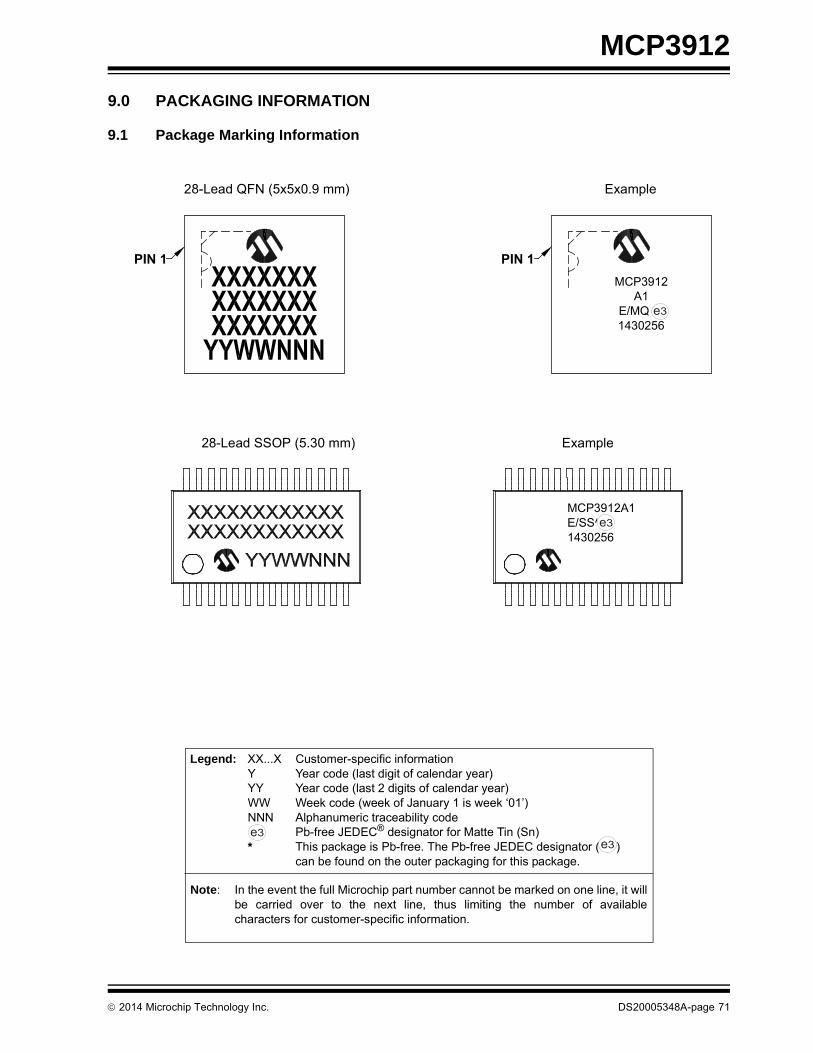
MCP3912
9.0 PACKAGING INFORMATION
9.1 Package Marking Information
Legend: XX...X Customer-specific informationY Year code (last digit of calendar year)YY Year code (last 2 digits of calendar year)WW Week code (week of January 1 is week ‘01’)NNN Alphanumeric traceability code Pb-free JEDEC® designator for Matte Tin (Sn)* This package is Pb-free. The Pb-free JEDEC designator ( )
can be found on the outer packaging for this package.
Note: In the event the full Microchip part number cannot be marked on one line, it willbe carried over to the next line, thus limiting the number of availablecharacters for customer-specific information.
3e
3e
28-Lead SSOP (5.30 mm) Example
MCP3912A1E/SS^^1430256
3e
28-Lead QFN (5x5x0.9 mm) Example
PIN 1 PIN 1MCP3912
A1E/MQ ^^1430256
3e
2014 Microchip Technology Inc. DS20005348A-page 71

MCP3912
���������� ��������������� ���������������� �!"���#
$ ��%�� ������!�"#�����$ %�& �'#� �(���!���)�*#'�(#"'�* �����' $�,�'����'� ���'�� $��� ���� ��( �"���"�����$�.��$����'�����#$ �(��$�&��"�������'�#"���"�����$�&��"�������'�#"���"�"�������'� %� $������((� ��"�$ �/� ��( �"���������$�'�� �������� �����.�:���;��
<�=> <�"�����( �"������� �� '������� %��'�!��# �"��,��,�'��#'�'�� ���� "��.?> � & � �� ���( �"���)�#"#�����,�'��#'�'�� ���� )�&�����&��(�'����#��" "������
$ �% ?���'� �(�"'��#�� �'���@�� �$��,���")�� �" �" �'� �������������@������� ��&���'��������' $��'��''>BB,,,�(����������(B��@�����
F��'" ��II��.�.����( �"����I�(�'" ��M MQ� ��V
M#(* ���&����" M �W��'�� ���;�<�=Q! �����Y ���' � Z Z �������$ $����@�� �����@� "" �� ���; ���; ��W;�'��$�&&� �� ���; Z ZQ! �����[�$'� . ���� ��W� W������$ $����@�� �[�$'� .� ;��� ;�/� ;���Q! �����I ��'� � ���� ����� ���;�?��'�I ��'� I ��;; ���; ���;?��'���' I� ���;��.?I �$�����@� "" � ���� Z ���;?��'����� � �\ �\ W\I �$�[�$'� * ���� Z ��/W
LL1
cA2
A1
A
EE1
D
N
1 2
NOTE 1b
e
φ
�������� � �������� ���,��� =����/<
DS20005348A-page 72 2014 Microchip Technology Inc.
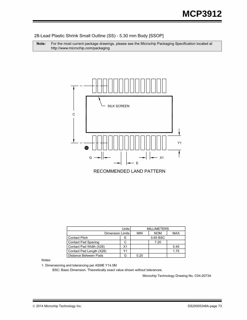
MCP3912
Note: For the most current package drawings, please see the Microchip Packaging Specification located at http://www.microchip.com/packaging
2014 Microchip Technology Inc. DS20005348A-page 73

MCP3912
BA
0.10 C
0.10 C
0.10 C A B0.05 C
(DATUM B)(DATUM A)
NOTE 1
2XTOP VIEW
SIDE VIEW
BOTTOM VIEW
For the most current package drawings, please see the Microchip Packaging Specification located athttp://www.microchip.com/packaging
Note:
NOTE 1
12
N
0.10 C A B
0.10 C A B
0.10 C
0.08 C
Microchip Technology Drawing C04-140C Sheet 1 of 2
28-Lead Plastic Quad Flat, No Lead Package (MQ) – 5x5x0.9 mm Body [QFN or VQFN]
2X
28X
D
E
12
N
e
28X L
28X K
E2
D2
28X b
A3
AC
SEATINGPLANE
A1
DS20005348A-page 74 2014 Microchip Technology Inc.
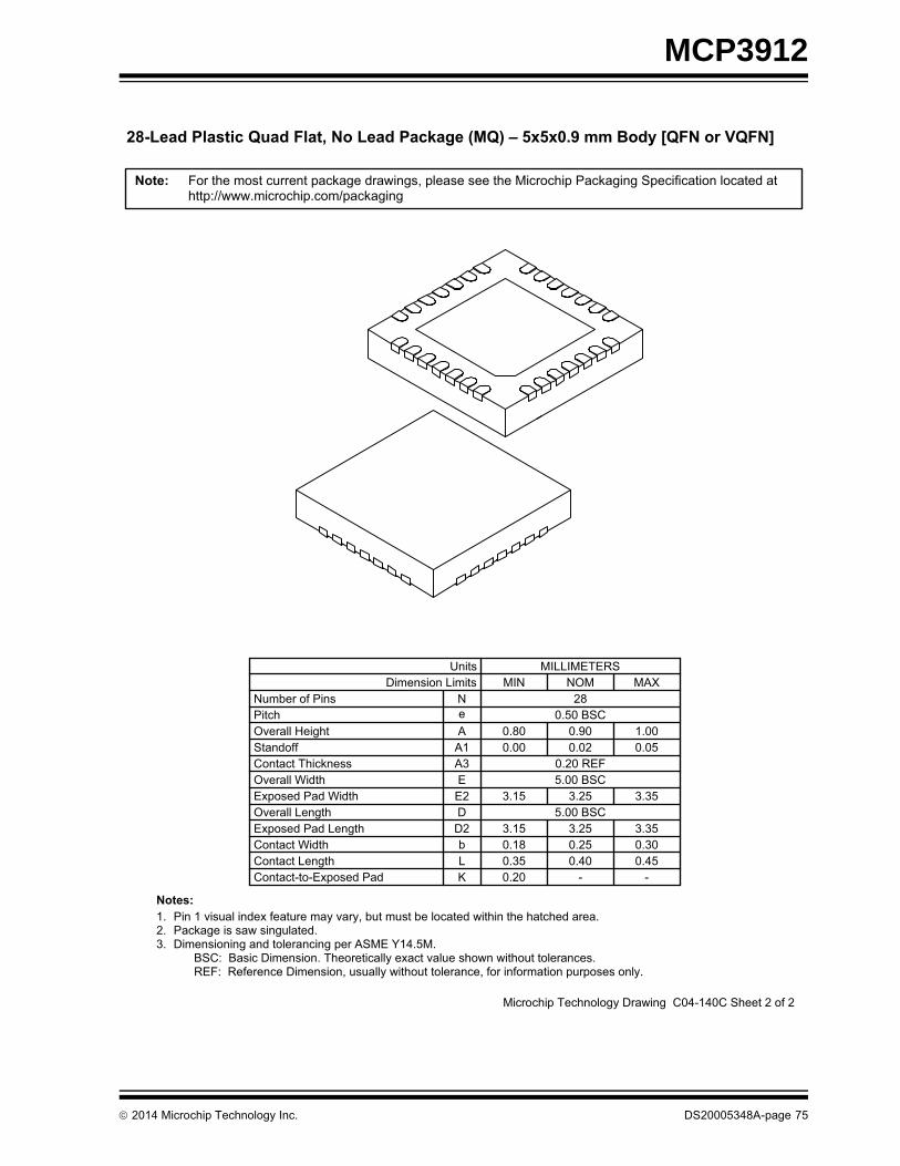
MCP3912
Microchip Technology Drawing C04-140C Sheet 2 of 2
For the most current package drawings, please see the Microchip Packaging Specification located athttp://www.microchip.com/packaging
Note:
28-Lead Plastic Quad Flat, No Lead Package (MQ) – 5x5x0.9 mm Body [QFN or VQFN]
Dimension LimitsUnits
D
Overall Width
Overall LengthExposed Pad Length
Exposed Pad Width
Contact Thickness
D2
E2E
3.35
MILLIMETERS
0.20 REF
MIN
A3
MAX
5.00 BSC3.25
Contact LengthContact Width
Lb
0.450.30
Notes:1.
KContact-to-Exposed Pad 0.20
NOM
BSC: Basic Dimension. Theoretically exact value shown without tolerances.3.2.
REF: Reference Dimension, usually without tolerance, for information purposes only.
Standoff A1 0.02Overall Height A 0.90Pitch e 0.50 BSCNumber of Pins N 28
0.350.183.15
3.15
0.000.80
0.250.40
-
3.255.00 BSC
3.35
0.051.00
-
Pin 1 visual index feature may vary, but must be located within the hatched area.
Dimensioning and tolerancing per ASME Y14.5M.Package is saw singulated.
2014 Microchip Technology Inc. DS20005348A-page 75
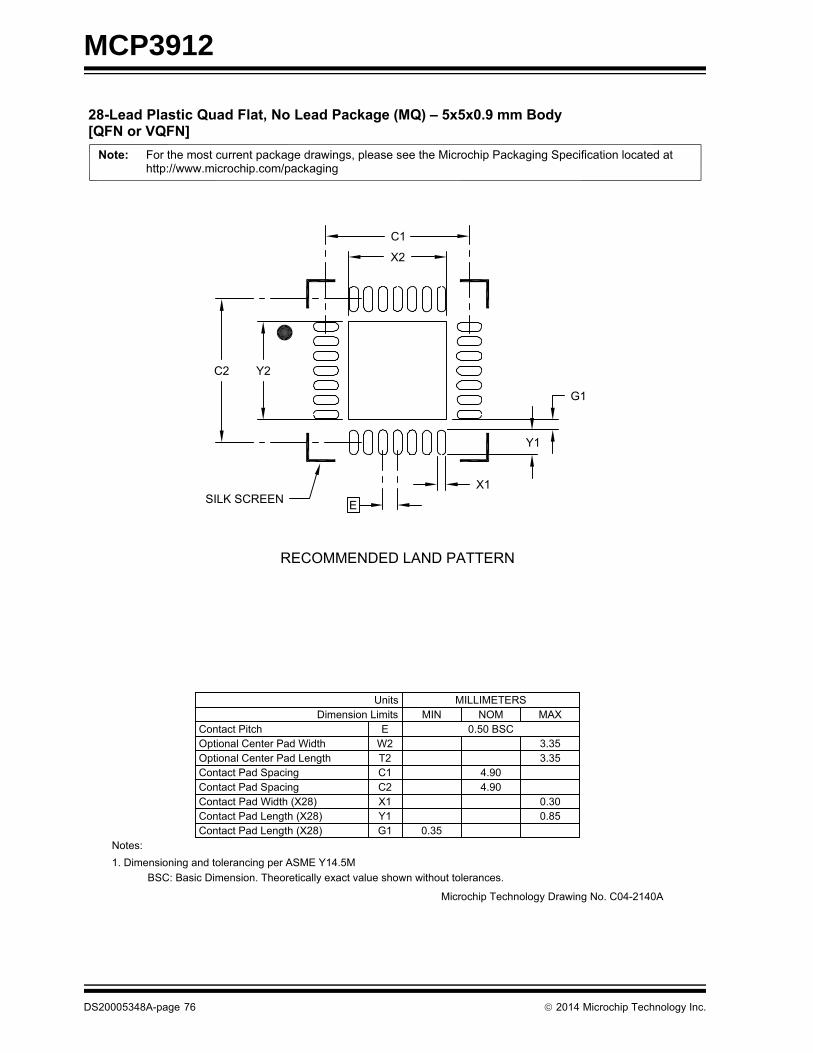
MCP3912
RECOMMENDED LAND PATTERN
28-Lead Plastic Quad Flat, No Lead Package (MQ) – 5x5x0.9 mm Body
Dimension LimitsUnits
C1
Optional Center Pad Width
Contact Pad SpacingContact Pad Spacing
Optional Center Pad Length
Contact Pitch
C2
T2W2
3.353.35
MILLIMETERS
0.50 BSCMIN
EMAX
4.904.90
Contact Pad Length (X28)Contact Pad Width (X28)
Y1X1
0.850.30
BSC: Basic Dimension. Theoretically exact value shown without tolerances.
Notes:1. Dimensioning and tolerancing per ASME Y14.5M
Microchip Technology Drawing No. C04-2140A
NOM
C1
C2 Y2
X2
Y1
G1
E
G1 0.35Contact Pad Length (X28)
SILK SCREEN
For the most current package drawings, please see the Microchip Packaging Specification located athttp://www.microchip.com/packaging
Note:
X1
[QFN or VQFN]
DS20005348A-page 76 2014 Microchip Technology Inc.

MCP3912
APPENDIX A: REVISION HISTORY
Revision A (September 2014)
• Original Release of this Document.
2014 Microchip Technology Inc. DS20005348A-page 77

MCP3912
NOTES:
2014 Microchip Technology Inc. DS20005348A-page 78

MCP3912
PRODUCT IDENTIFICATION SYSTEM
To order or obtain information, e.g., on pricing or delivery, refer to the factory or the listed sales office.
Device: MCP3912: Four-Channel Analog Front-End Converter
Address Options: XX A6 A5
A0 = 0 0
A1* = 0 1
A2 = 1 0
A3 = 1 1
* Default option. Contact Microchip factory for other address options.
Tape and Reel Option: Blank = Standard packaging (tube or tray)
T = Tape and Reel(1)
Temperature Range: E = -40°C to +125°C
Package: MQ = Plastic Quad Flat, No Lead package (QFN)SS = Plastic Shrink Small Outline, 5.30 mm body
(SSOP)
Examples:
a) MCP3912A1-E/SS: Address Option A1,Extended Temperature,28LD SSOP package
b) MCP3912A1T-E/SS: Address Option A1,Tape and Reel,Extended Temperature,28LD SSOP package
c) MCP3912A1-E/MQ: Address Option A1,Extended Temperature,28LD QFN package
d) MCP3912A1T-E/MQ: Address Option A1,Tape and Reel,Extended Temperature,28LD QFN package
PART NO. X
TemperatureRange
Device
/XX
Package
[X](1)
Tape andReel
Note 1: Tape and Reel identifier only appears in the catalog part number description. This identi-fier is used for ordering purposes and is not printed on the device package. Check with your Microchip sales office for package availability for the Tape and Reel option.
XX
AddressOption
2014 Microchip Technology Inc. DS20005348A-page 79

MCP3912
NOTES:
2014 Microchip Technology Inc. DS20005348A-page 80

Note the following details of the code protection feature on Microchip devices:
• Microchip products meet the specification contained in their particular Microchip Data Sheet.
• Microchip believes that its family of products is one of the most secure families of its kind on the market today, when used in the intended manner and under normal conditions.
• There are dishonest and possibly illegal methods used to breach the code protection feature. All of these methods, to our knowledge, require using the Microchip products in a manner outside the operating specifications contained in Microchip’s Data Sheets. Most likely, the person doing so is engaged in theft of intellectual property.
• Microchip is willing to work with the customer who is concerned about the integrity of their code.
• Neither Microchip nor any other semiconductor manufacturer can guarantee the security of their code. Code protection does not mean that we are guaranteeing the product as “unbreakable.”
Code protection is constantly evolving. We at Microchip are committed to continuously improving the code protection features of ourproducts. Attempts to break Microchip’s code protection feature may be a violation of the Digital Millennium Copyright Act. If such actsallow unauthorized access to your software or other copyrighted work, you may have a right to sue for relief under that Act.
Information contained in this publication regarding deviceapplications and the like is provided only for your convenienceand may be superseded by updates. It is your responsibility toensure that your application meets with your specifications.MICROCHIP MAKES NO REPRESENTATIONS ORWARRANTIES OF ANY KIND WHETHER EXPRESS ORIMPLIED, WRITTEN OR ORAL, STATUTORY OROTHERWISE, RELATED TO THE INFORMATION,INCLUDING BUT NOT LIMITED TO ITS CONDITION,QUALITY, PERFORMANCE, MERCHANTABILITY ORFITNESS FOR PURPOSE. Microchip disclaims all liabilityarising from this information and its use. Use of Microchipdevices in life support and/or safety applications is entirely atthe buyer’s risk, and the buyer agrees to defend, indemnify andhold harmless Microchip from any and all damages, claims,suits, or expenses resulting from such use. No licenses areconveyed, implicitly or otherwise, under any Microchipintellectual property rights.
2014 Microchip Technology Inc.
QUALITY MANAGEMENT SYSTEM CERTIFIED BY DNV
== ISO/TS 16949 ==
Trademarks
The Microchip name and logo, the Microchip logo, dsPIC, FlashFlex, flexPWR, JukeBlox, KEELOQ, KEELOQ logo, Kleer, LANCheck, MediaLB, MOST, MOST logo, MPLAB, OptoLyzer, PIC, PICSTART, PIC32 logo, RightTouch, SpyNIC, SST, SST Logo, SuperFlash and UNI/O are registered trademarks of Microchip Technology Incorporated in the U.S.A. and other countries.
The Embedded Control Solutions Company and mTouch are registered trademarks of Microchip Technology Incorporated in the U.S.A.
Analog-for-the-Digital Age, BodyCom, chipKIT, chipKIT logo, CodeGuard, dsPICDEM, dsPICDEM.net, ECAN, In-Circuit Serial Programming, ICSP, Inter-Chip Connectivity, KleerNet, KleerNet logo, MiWi, MPASM, MPF, MPLAB Certified logo, MPLIB, MPLINK, MultiTRAK, NetDetach, Omniscient Code Generation, PICDEM, PICDEM.net, PICkit, PICtail, RightTouch logo, REAL ICE, SQI, Serial Quad I/O, Total Endurance, TSHARC, USBCheck, VariSense, ViewSpan, WiperLock, Wireless DNA, and ZENA are trademarks of Microchip Technology Incorporated in the U.S.A. and other countries.
SQTP is a service mark of Microchip Technology Incorporated in the U.S.A.
Silicon Storage Technology is a registered trademark of Microchip Technology Inc. in other countries.
GestIC is a registered trademarks of Microchip Technology Germany II GmbH & Co. KG, a subsidiary of Microchip Technology Inc., in other countries.
All other trademarks mentioned herein are property of their respective companies.
© 2014, Microchip Technology Incorporated, Printed in the U.S.A., All Rights Reserved.
ISBN: 978-1-63276-645-8
Microchip received ISO/TS-16949:2009 certification for its worldwide
DS20005348A-page 81
headquarters, design and wafer fabrication facilities in Chandler and Tempe, Arizona; Gresham, Oregon and design centers in California and India. The Company’s quality system processes and procedures are for its PIC® MCUs and dsPIC® DSCs, KEELOQ® code hopping devices, Serial EEPROMs, microperipherals, nonvolatile memory and analog products. In addition, Microchip’s quality system for the design and manufacture of development systems is ISO 9001:2000 certified.

DS20005348A-page 82 2014 Microchip Technology Inc.
AMERICASCorporate Office2355 West Chandler Blvd.Chandler, AZ 85224-6199Tel: 480-792-7200 Fax: 480-792-7277Technical Support: http://www.microchip.com/supportWeb Address: www.microchip.com
AtlantaDuluth, GA Tel: 678-957-9614 Fax: 678-957-1455
Austin, TXTel: 512-257-3370
BostonWestborough, MA Tel: 774-760-0087 Fax: 774-760-0088
ChicagoItasca, IL Tel: 630-285-0071 Fax: 630-285-0075
ClevelandIndependence, OH Tel: 216-447-0464 Fax: 216-447-0643
DallasAddison, TX Tel: 972-818-7423 Fax: 972-818-2924
DetroitNovi, MI Tel: 248-848-4000
Houston, TX Tel: 281-894-5983
IndianapolisNoblesville, IN Tel: 317-773-8323Fax: 317-773-5453
Los AngelesMission Viejo, CA Tel: 949-462-9523 Fax: 949-462-9608
New York, NY Tel: 631-435-6000
San Jose, CA Tel: 408-735-9110
Canada - TorontoTel: 905-673-0699 Fax: 905-673-6509
ASIA/PACIFICAsia Pacific OfficeSuites 3707-14, 37th FloorTower 6, The GatewayHarbour City, KowloonHong KongTel: 852-2943-5100Fax: 852-2401-3431
Australia - SydneyTel: 61-2-9868-6733Fax: 61-2-9868-6755
China - BeijingTel: 86-10-8569-7000 Fax: 86-10-8528-2104
China - ChengduTel: 86-28-8665-5511Fax: 86-28-8665-7889
China - ChongqingTel: 86-23-8980-9588Fax: 86-23-8980-9500
China - HangzhouTel: 86-571-8792-8115 Fax: 86-571-8792-8116
China - Hong Kong SARTel: 852-2943-5100 Fax: 852-2401-3431
China - NanjingTel: 86-25-8473-2460Fax: 86-25-8473-2470
China - QingdaoTel: 86-532-8502-7355Fax: 86-532-8502-7205
China - ShanghaiTel: 86-21-5407-5533 Fax: 86-21-5407-5066
China - ShenyangTel: 86-24-2334-2829Fax: 86-24-2334-2393
China - ShenzhenTel: 86-755-8864-2200 Fax: 86-755-8203-1760
China - WuhanTel: 86-27-5980-5300Fax: 86-27-5980-5118
China - XianTel: 86-29-8833-7252Fax: 86-29-8833-7256
China - XiamenTel: 86-592-2388138 Fax: 86-592-2388130
China - ZhuhaiTel: 86-756-3210040 Fax: 86-756-3210049
ASIA/PACIFICIndia - BangaloreTel: 91-80-3090-4444 Fax: 91-80-3090-4123
India - New DelhiTel: 91-11-4160-8631Fax: 91-11-4160-8632
India - PuneTel: 91-20-3019-1500
Japan - OsakaTel: 81-6-6152-7160 Fax: 81-6-6152-9310
Japan - TokyoTel: 81-3-6880- 3770 Fax: 81-3-6880-3771
Korea - DaeguTel: 82-53-744-4301Fax: 82-53-744-4302
Korea - SeoulTel: 82-2-554-7200Fax: 82-2-558-5932 or 82-2-558-5934
Malaysia - Kuala LumpurTel: 60-3-6201-9857Fax: 60-3-6201-9859
Malaysia - PenangTel: 60-4-227-8870Fax: 60-4-227-4068
Philippines - ManilaTel: 63-2-634-9065Fax: 63-2-634-9069
SingaporeTel: 65-6334-8870Fax: 65-6334-8850
Taiwan - Hsin ChuTel: 886-3-5778-366Fax: 886-3-5770-955
Taiwan - KaohsiungTel: 886-7-213-7830
Taiwan - TaipeiTel: 886-2-2508-8600 Fax: 886-2-2508-0102
Thailand - BangkokTel: 66-2-694-1351Fax: 66-2-694-1350
EUROPEAustria - WelsTel: 43-7242-2244-39Fax: 43-7242-2244-393Denmark - CopenhagenTel: 45-4450-2828 Fax: 45-4485-2829
France - ParisTel: 33-1-69-53-63-20 Fax: 33-1-69-30-90-79
Germany - DusseldorfTel: 49-2129-3766400
Germany - MunichTel: 49-89-627-144-0 Fax: 49-89-627-144-44
Germany - PforzheimTel: 49-7231-424750
Italy - Milan Tel: 39-0331-742611 Fax: 39-0331-466781
Italy - VeniceTel: 39-049-7625286
Netherlands - DrunenTel: 31-416-690399 Fax: 31-416-690340
Poland - WarsawTel: 48-22-3325737
Spain - MadridTel: 34-91-708-08-90Fax: 34-91-708-08-91
Sweden - StockholmTel: 46-8-5090-4654
UK - WokinghamTel: 44-118-921-5800Fax: 44-118-921-5820
Worldwide Sales and Service
03/25/14