MC3210 Datasheet - dzsc.comfile1.dzsc.com/product/14/11/13/824138_120206482.pdf · Acceleration,...
73
MC3210 3-Axis Accelerometer Datasheet mCube Proprietary and Confidential. APS-048-0005v1.1 1 / 73 © 2011 mCube Inc. All rights reserved. M3210A 9B249M 117AA GENERAL DESCRIPTION The MC3210 Series is a low-noise, integrated digital output 3-axis accelerometers with a feature set optimized for cell phones and consumer product motion sensing. Applications include user interface control, gaming motion input, and electronic compass tilt compensation for cell phones, game controllers, remote controls and portable media products. Accurate event detection is enabled with a low noise architecture that minimizes false triggering found in competing devices. Low noise and low power are inherent in the monolithic fabrication approach, where the MEMS accelerometer is integrated in a single-chip with the electronics integrated circuit. In the MC3210 the internal sample rate is fixed at 1024 samples / second. Specific orientation and gesture conditions can trigger an interrupt to a remote MCU. Alternatively, the device supports the reading of sample and event status via polling. FEATURES Range, Sampling & Power ± 2g / ± 4g / ± 8g ranges 10-bit or 14-bit resolution 1024 samples/sec Programmable low pass filter ‒ From 8 to 512 Hz bandwidth 200 μA current draw Event Detection Low-noise architecture minimizes false triggering Tap, Shake, Drop Portrait or landscape orientation with programmable hysteresis Tilt detection in six orientations Simple System Integration I2C interface, up to 400 kHz 3 × 3 × 1.0 mm 10-pin VDFN package ‒ Pin-compatible to popular footprints Single-chip 3D silicon MEMS
Transcript of MC3210 Datasheet - dzsc.comfile1.dzsc.com/product/14/11/13/824138_120206482.pdf · Acceleration,...

MC3210 3-Axis Accelerometer Datasheet
mCube Proprietary and Confidential. APS-048-0005v1.1 1 / 73 © 2011 mCube Inc. All rights reserved.
M3210A9B249M 117AA
GENERAL DESCRIPTION
The MC3210 Series is a low-noise, integrated digital output 3-axis accelerometers with a feature set optimized for cell phones and consumer product motion sensing. Applications include user interface control, gaming motion input, and electronic compass tilt compensation for cell phones, game controllers, remote controls and portable media products.
Accurate event detection is enabled with a low noise architecture that minimizes false triggering found in competing devices. Low noise and low power are inherent in the monolithic fabrication approach, where the MEMS accelerometer is integrated in a single-chip with the electronics integrated circuit.
In the MC3210 the internal sample rate is fixed at 1024 samples / second. Specific orientation and gesture conditions can trigger an interrupt to a remote MCU. Alternatively, the device supports the reading of sample and event status via polling.
FEATURES
Range, Sampling & Power
± 2g / ± 4g / ± 8g ranges 10-bit or 14-bit resolution 1024 samples/sec Programmable low pass filter
‒ From 8 to 512 Hz bandwidth
200 μA current draw
Event Detection
Low-noise architecture minimizes false triggering
Tap, Shake, Drop Portrait or landscape orientation with
programmable hysteresis Tilt detection in six orientations
Simple System Integration
I2C interface, up to 400 kHz 3 × 3 × 1.0 mm 10-pin VDFN
package ‒ Pin-compatible to popular footprints
Single-chip 3D silicon MEMS

MC3210 3-Axis Accelerometer Datasheet
mCube Proprietary and Confidential. APS-048-0005v1.1 2 / 73 © 2011 mCube Inc. All rights reserved.
TABLE OF CONTENTS 1 ORDER INFORMATION .................................................................................................. 5
2 Functional Block Diagram ................................................................................................ 6
3 Packaging and Pin Description ........................................................................................ 7
3.1 Package Outline ................................................................................................................... 7
3.2 Pin Description ..................................................................................................................... 8
3.3 TYPICAL APPLICATION CIRCUIT ...................................................................................... 9
4 Specifications ................................................................................................................. 10
4.1 Absolute Maximum Ratings ................................................................................................ 10
4.2 Sensor Characteristics ....................................................................................................... 11
4.3 Electrical and Timing Characteristics .................................................................................. 12
4.3.1 Electrical Power and Internal Characteristics ....................................................... 12
4.3.2 I2C Electrical Characteristics ............................................................................... 13
4.3.3 I2C Timing Characteristics ................................................................................... 14
5 General Operation ......................................................................................................... 15
5.1 Sensor Sampling ................................................................................................................ 15
5.2 offset and gain calibration .................................................................................................. 16
6 Operational States ......................................................................................................... 17
7 Operational State Flow .................................................................................................. 18
8 Interrupts ........................................................................................................................ 19
8.1 Enabling and Clearing Interrupts ........................................................................................ 19
8.2 Interrupt Support ................................................................................................................ 20
8.3 GINT Interrupt .................................................................................................................... 21
8.4 Event Detection .................................................................................................................. 22
9 Orientation Detection ..................................................................................................... 23
9.1 Orientation Hysteresis ........................................................................................................ 23
9.2 Portrait/Landscape Events ................................................................................................. 23
9.3 Front/Back Events .............................................................................................................. 28
9.4 Shake Detection ................................................................................................................. 30
9.5 Drop Detection ................................................................................................................... 32

MC3210 3-Axis Accelerometer Datasheet
mCube Proprietary and Confidential. APS-048-0005v1.1 3 / 73 © 2011 mCube Inc. All rights reserved.
9.6 Tap Detection ..................................................................................................................... 33
9.7 Continuous Sampling ......................................................................................................... 35
10 I2C Interface .................................................................................................................. 36
10.1 Physical Interface ............................................................................................................... 36
10.2 Timing ................................................................................................................................ 36
10.3 I2C Message Format .......................................................................................................... 36
11 Register Interface .......................................................................................................... 38
11.1 Register Summary ............................................................................................................. 39
11.2 TILT: Status Register ......................................................................................................... 41
11.3 OPSTAT: Operational State Status Register ...................................................................... 43
11.4 INTEN: Interrupt Enable Register ....................................................................................... 44
11.5 MODE: Register ................................................................................................................. 45
11.6 TAPEN: Tap Detection Enable Register ............................................................................. 46
11.7 TAPP: Tap Pulse Register ................................................................................................. 47
11.8 DROP: Drop Event Control Register .................................................................................. 48
11.9 SHDB: Shake Debounce Register ...................................................................................... 49
11.10 XOUT_EX, YOUT_EX & ZOUT_EX: X, Y, Z-Axis Extended Accelerometer Registers ....... 50
11.11 CHIPID: Chip Identification Register ................................................................................... 51
11.12 OUTCFG: Output Configuration Register ........................................................................... 52
11.13 X-Axis Offset Registers ...................................................................................................... 53
11.14 Y-Axis Offset Registers ...................................................................................................... 54
11.15 Z-Axis Offset Registers ...................................................................................................... 55
11.16 X-Axis Gain Registers ........................................................................................................ 56
11.17 Y-Axis Gain Registers ........................................................................................................ 57
11.18 Z-Axis Gain Registers ........................................................................................................ 58
11.19 SHAKE_TH: Shake Threshold Register ............................................................................. 59
11.20 UD_Z_TH: Up/Down Z Axis Threshold Register ................................................................. 60
11.21 UD_X_TH: Up/Down X Axis Threshold Register ................................................................ 61
11.22 RL_Z_TH: Right/Left Z Axis Threshold Register ................................................................. 62
11.23 RL_Y_TH: Right/Left Y Axis Threshold Register ................................................................ 63
11.24 FB_Z_TH: Front/Back Z Axis Threshold Register ............................................................... 64
11.25 DROP_TH: Drop Threshold Register ................................................................................. 65
11.26 TAP_TH: Tap Threshold Register ...................................................................................... 66
11.27 PCODE: Product Code....................................................................................................... 67
MC3210 3-Axis Accelerometer Datasheet
mCube Proprietary and Confidential. APS-048-0005v1.1 4 / 73 © 2011 mCube Inc. All rights reserved.
12 Example MC3210 Configuration .................................................................................... 68
12.1 Example: Shake, Tap & Drop thresholds Demo ................................................................. 68
13 Index of Tables .............................................................................................................. 70
14 Revision History ............................................................................................................. 72
15 Legal .............................................................................................................................. 73
MC3210 3-Axis Accelerometer Datasheet
mCube Proprietary and Confidential. APS-048-0005v1.1 5 / 73 © 2011 mCube Inc. All rights reserved.
1 ORDER INFORMATION
Table 1. Order Information
Part Number Resolution Order Number Package Shipping
MC3210 10 or 14-bit MC3210-I5 VDFN-10 Tape & Reel, 5Ku
MC3210 3-Axis Accelerometer Datasheet
mCube Proprietary and Confidential. APS-048-0005v1.1 6 / 73 © 2011 mCube Inc. All rights reserved.
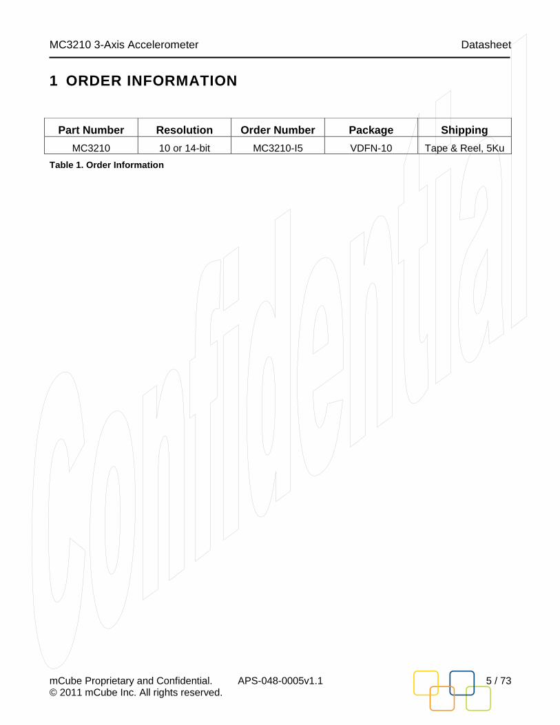
2 FUNCTIONAL BLOCK DIAGRAM
Orientation
and
Detection
Logic
A/D Converter
(Sigma Delta)C to V
VPP
AVDD
DVDD
GND
Regulator
Oscillator/
Clock
Generator
Mode Logic
I2C Slave
Interface
Interrupt
Detection
Bias
Generator
X
A/D Converter
(Sigma Delta)C to VY
A/D Converter
(Sigma Delta)
Offset/
Gain
Adjust
C to VZOTP
Memory
Registers
(64 x 8)
SCL
SDA
TEST
INTN
Range,
Resolution
LPF[2:0]
Offset/
Gain
Adjust
Offset/
Gain
Adjust
XOUT_EX,
YOUT_EX,
ZOUT_EX
Various events
X,Y,Z data paths
14-bit
Sensors
10-bit
Figure 1. Block Diagram
MC3210 3-Axis Accelerometer Datasheet
mCube Proprietary and Confidential. APS-048-0005v1.1 7 / 73 © 2011 mCube Inc. All rights reserved.
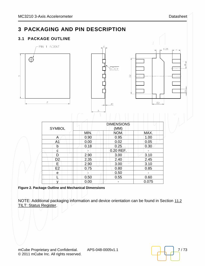
3 PACKAGING AND PIN DESCRIPTION
3.1 PACKAGE OUTLINE
SYMBOL DIMENSIONS
(MM)
MIN. NOM. MAX.
A 0.90 0.95 1.00
A1 0.00 0.02 0.05
b 0.18 0.25 0.30
c - 0.20 REF. -
D 2.90 3.00 3.10
D2 2.35 2.40 2.45
E 2.90 3.00 3.10
E2 0.75 0.80 0.85
e - 0.50 -
L 0.50 0.55 0.60
y 0.00 - 0.075
Figure 2. Package Outline and Mechanical Dimensions
NOTE: Additional packaging information and device orientation can be found in Section 11.2 TILT: Status Register.

MC3210 3-Axis Accelerometer Datasheet
mCube Proprietary and Confidential. APS-048-0005v1.1 8 / 73 © 2011 mCube Inc. All rights reserved.
3.2 PIN DESCRIPTION
Pin Name Function
1 NC No connect
2 TEST Optional probe pin
3 AVDD Analog power supply
4 VPP Connect to GND
5 INTN 2 Interrupt input/output, active
LOW 3
6 SCK 1 I2C serial clock input
7 SDA 1 I2C serial data input/output
8 GND Ground
9 DVDD I/O power supply
10 NC No connect
Table 2. Pin Description
Notes:
1) This pin requires a pull-up resistor, typically 4.7kΩ to DVDD. Refer to I2C Specification for Fast-Mode devices. Higher resistance values can be used (typically done to reduce current leakage) but such applications are outside the scope of this datasheet.
2) This pin can be configured by software to operate either as an open-drain output or push-pull output (MODE: Register). If set to open-drain, then it requires a pull-up resistor, typically 4.7kΩ to DVDD.
3) INTN pin polarity is programmable in the MODE: Register.

MC3210 3-Axis Accelerometer Datasheet
mCube Proprietary and Confidential. APS-048-0005v1.1 9 / 73 © 2011 mCube Inc. All rights reserved.
3.3 TYPICAL APPLICATION CIRCUIT
0.1uF
Place cap close
to AVDD and
GND on PCB
To Fast-Mode I2C
circuitry1
(optional) To MCU
interrupt input2
0.1uF
Place cap close
to DVDD and
GND on PCB
NC
AVDD
GND
TEST
VPP
NC
DVDD
SDA
SCL
INTN
From interface
power supply
NOTE1: Attach typical 4.7kΩ pullup resistors to DVDD, per I2C specification. When
DVDD is powered down, SDA and SCL will be driven low by internal ESD diodes.
NOTE2: Attach typical 4.7kΩ pullup resistor if INTN is defined as open-drain.
From lower-noise
power supply
Figure 3. Typical Application Circuit
In typical applications, the interface power supply may contain significant noise from external sources and other circuits which should be kept away from the sensor. Therefore, for some applications a lower-noise power supply might be desirable to power the AVDD pin.

MC3210 3-Axis Accelerometer Datasheet
mCube Proprietary and Confidential. APS-048-0005v1.1 10 / 73 © 2011 mCube Inc. All rights reserved.
4 SPECIFICATIONS
4.1 ABSOLUTE MAXIMUM RATINGS
Parameters exceeding the Absolute Maximum Ratings may permanently damage the device.
Rating Symbol Minimum / Maximum
Value Unit
Supply Voltages Pins DVDD and
AVDD -0.3 / +3.6 V
Acceleration, any axis, 100 µs g MAX 10000 g
Ambient operating temperature TOP -40 / +85 ⁰C
Storage temperature TSTG -40 / +125 ⁰C
ESD human body model HBM ± 2000 V
Latch-up current at Top = 25 ⁰C ILU 200 mA
Input voltage to non-power pin Pins INTN, SCL
and SDA -0.3 / (DVDD + 0.3) or 3.6
whichever is lower V
Table 3. Absolute Maximum Ratings
MC3210 3-Axis Accelerometer Datasheet
mCube Proprietary and Confidential. APS-048-0005v1.1 11 / 73 © 2011 mCube Inc. All rights reserved.
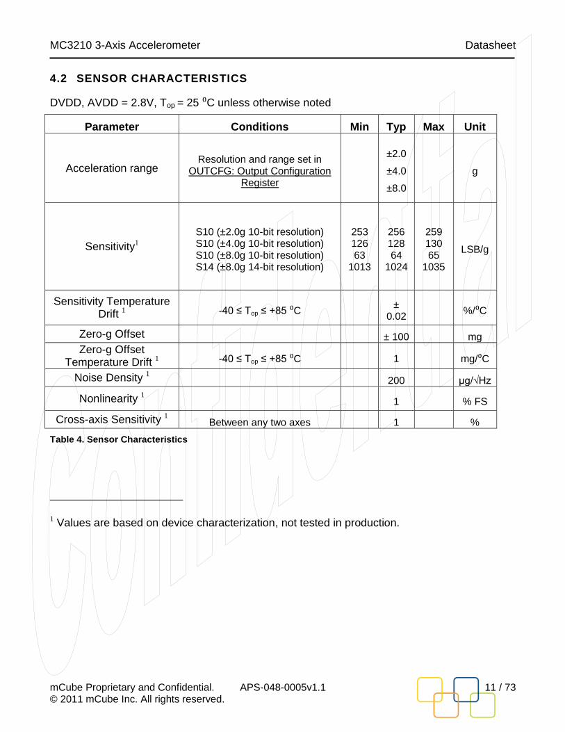
4.2 SENSOR CHARACTERISTICS
DVDD, AVDD = 2.8V, Top = 25 ⁰C unless otherwise noted
Parameter Conditions Min Typ Max Unit
Acceleration range Resolution and range set in
OUTCFG: Output Configuration Register
±2.0
±4.0
±8.0
g
Sensitivity1
S10 (±2.0g 10-bit resolution) S10 (±4.0g 10-bit resolution) S10 (±8.0g 10-bit resolution) S14 (±8.0g 14-bit resolution)
253 126 63
1013
256 128 64
1024
259 130 65
1035
LSB/g
Sensitivity Temperature Drift 1 -40 ≤ Top ≤ +85 ⁰C
± 0.02
%/⁰C
Zero-g Offset ± 100 mg
Zero-g Offset Temperature Drift 1 -40 ≤ Top ≤ +85 ⁰C 1 mg/⁰C
Noise Density 1 200 μg/√Hz
Nonlinearity 1 1 % FS
Cross-axis Sensitivity 1 Between any two axes 1 %
Table 4. Sensor Characteristics
1 Values are based on device characterization, not tested in production.
MC3210 3-Axis Accelerometer Datasheet
mCube Proprietary and Confidential. APS-048-0005v1.1 12 / 73 © 2011 mCube Inc. All rights reserved.
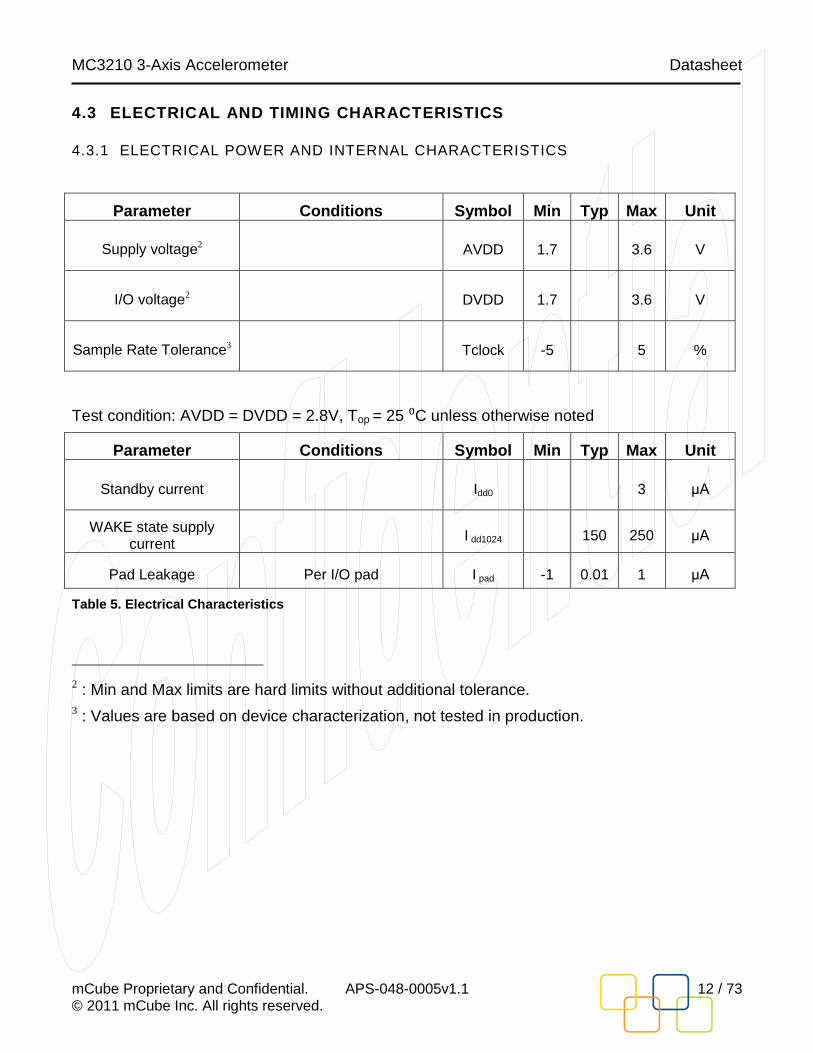
4.3 ELECTRICAL AND TIMING CHARACTERISTICS
4.3.1 ELECTRICAL POWER AND INTERNAL CHARACTERISTICS
Parameter Conditions Symbol Min Typ Max Unit
Supply voltage2
AVDD 1.7 3.6 V
I/O voltage2
DVDD 1.7 3.6 V
Sample Rate Tolerance3
Tclock -5 5 %
Test condition: AVDD = DVDD = 2.8V, Top = 25 ⁰C unless otherwise noted
Parameter Conditions Symbol Min Typ Max Unit
Standby current
Idd0 3 μA
WAKE state supply current
I dd1024 150 250 μA
Pad Leakage Per I/O pad I pad -1 0.01 1 μA
Table 5. Electrical Characteristics
2 : Min and Max limits are hard limits without additional tolerance.
3 : Values are based on device characterization, not tested in production.

MC3210 3-Axis Accelerometer Datasheet
mCube Proprietary and Confidential. APS-048-0005v1.1 13 / 73 © 2011 mCube Inc. All rights reserved.
4.3.2 I2C ELECTRICAL CHARACTERISTICS
Parameter Symbol Min Max Unit
LOW level input voltage VIL -0.5 0.3*DVDD V
HIGH level input voltage VIH 0.7*DVDD - V
Hysteresis of Schmitt trigger inputs Vhys 0.05*DVDD - V
Output voltage, pin INTN, Iol ≤ 2 mA Vol
Voh
0
0
0.4
0.9*DVDD
V
V
Output voltage, pin SDA (open drain), Iol ≤ 1 mA Vols - 0.1*DVDD V
Input current, pins SDA and SCL (input voltage between 0.1*DVDD and 0.9*DVDD max) Ii -10 10 µA
Capacitance, pins SDA and SCL4 Ci - 10 pF
Table 6. I2C Electrical and Timing Characteristics
NOTES:
If multiple slaves are connected to the I2C signals in addition to this device, only 1 pull-up resistor on each of SDA and SCL should exist. Also, care must be taken to not violate the I2C specification for capacitive loading.
When DVDD is not powered and set to 0V, INTN, SDA and SCL will be held to DVDD plus the forward voltage of the internal static protection diodes, typically about 0.6V.
When DVDD is disconnected from power or ground (e.g. Hi-Z), the device may become inadvertently powered up through the ESD diodes present on other powered signals.
4 : Values are based on device characterization, not tested in production.
MC3210 3-Axis Accelerometer Datasheet
mCube Proprietary and Confidential. APS-048-0005v1.1 14 / 73 © 2011 mCube Inc. All rights reserved.
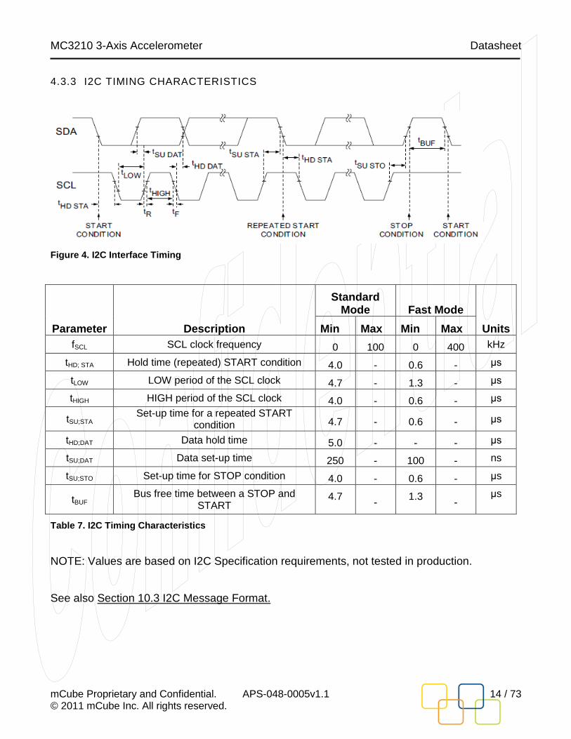
4.3.3 I2C TIMING CHARACTERISTICS
Figure 4. I2C Interface Timing
Parameter Description
Standard Mode Fast Mode
Units Min Max Min Max
fSCL SCL clock frequency 0 100 0 400 kHz
tHD; STA Hold time (repeated) START condition 4.0 - 0.6 - μs
tLOW LOW period of the SCL clock 4.7 - 1.3 - μs
tHIGH HIGH period of the SCL clock 4.0 - 0.6 - μs
tSU;STA Set-up time for a repeated START
condition 4.7 - 0.6 - μs
tHD;DAT Data hold time 5.0 - - - μs
tSU;DAT Data set-up time 250 - 100 - ns
tSU;STO Set-up time for STOP condition 4.0 - 0.6 - μs
tBUF Bus free time between a STOP and
START 4.7
-
1.3
- μs
Table 7. I2C Timing Characteristics
NOTE: Values are based on I2C Specification requirements, not tested in production.
See also Section 10.3 I2C Message Format.

MC3210 3-Axis Accelerometer Datasheet
mCube Proprietary and Confidential. APS-048-0005v1.1 15 / 73 © 2011 mCube Inc. All rights reserved.
5 GENERAL OPERATION
The internal sampling rate range is fixed at 1024 samples per second. The resulting sensor readings appear as either 10-bit or 14-bit values, depending upon the selection chosen.
5.1 SENSOR SAMPLING
Measurement data is stored in the “extended” registers XOUT_EX, YOUT_EX, and ZOUT_EX. The byte with the lower address of the byte pair is the least significant byte while the byte with the next higher address is the most significant byte. The 10-bit or 14-bit measurement is represented as 2‟s complement format.
10-bit samples occupy bits [9:0], with bits [15:9] occupied by the sign bit.
14-bit samples occupy bits [13:0], with bits [15:13] occupied by the sign bit.
The desired resolution and full scale acceleration range of ± 2g, ± 4g or ± 8g are set in OUTCFG: Output Configuration Register.
The device sample rate is fixed at 1024 samples/second. The features Tap, Shake, Drop and Orientation detection are available.
Resolution
Acceleration
Range
Value per bit
(mg/LSB)
Full Scale Negative Reading
Full Scale Positive Reading Comments
10-bit ± 2g ~3.9
0xFE00
(-512)
0x01FF
(+511)
Signed, 2‟s complement number, results in registers XOUT_EX_L, XOUT_EX_H YOUT_EX_L, YOUT_EX_H ZOUT_EX_L, ZOUT_EX_H
(Sign-extended. Integer interpretation also shown)
10-bit ± 4g ~7.8
10-bit ± 8g ~15.6
14-bit ± 8g ~0.98 0xE000
(-8192)
0x1FFF
(+8191)
Signed, 2‟s complement number, results in registers XOUT_EX_L, XOUT_EX_H YOUT_EX_L, YOUT_EX_H ZOUT_EX_L, ZOUT_EX_H
(Sign-extended. Integer interpretation also shown)
Table 8. Summary of Resolution, Range, and Scaling
Based upon the intended application, filtering of the data samples may be desired. The device has several low-pass filter (LPF) options for the raw sample data, intended to filter out
MC3210 3-Axis Accelerometer Datasheet
mCube Proprietary and Confidential. APS-048-0005v1.1 16 / 73 © 2011 mCube Inc. All rights reserved.
undesired high frequency components. Related to this LPF setting is the GINT interrupt rate, which can be modified to occur based upon the LPF roll-off frequency, rather than the sample rate (fixed at 1024 samples / second). See Section 8.2 GINT Interrupt for more on this option. The cutoff points for the LPF can be set from 8Hz to 512 Hz. These, and the controls for the GINT rate, are described in Section 11.12 OUTCFG: Output Configuration Register.
5.2 OFFSET AND GAIN CALIBRATION
Digital offset and gain calibration can be performed on the sensor, if necessary, in order to reduce the effects of post-assembly influences and stresses which may cause the sensor readings to be offset from their factory values. The register controls are described in Sections 11.13 through 11.18.
MC3210 3-Axis Accelerometer Datasheet
mCube Proprietary and Confidential. APS-048-0005v1.1 17 / 73 © 2011 mCube Inc. All rights reserved.
6 OPERATIONAL STATES
The device has two states of operation: STANDBY (the default state after power-up), and WAKE.
The STANDBY state offers the lowest power consumption. In this state, the I2C interface is active and all register reads and writes are allowed. There is no event detection, sampling, or acceleration measurement in the STANDBY state. Internal clocking is halted. Complete access to the register set is allowed in this state, but interrupts cannot be serviced. The device defaults to the STANDBY state following power-up. The time to change states from STANDBY to WAKE is less than 10uSec and does not depend upon the sample rate.
Registers can be written (and therefore resolution, range. thresholds and other settings changed) only when the device is in STANDBY state.
The I2C interface allows write access to all registers only in the STANDBY state. In WAKE state, the only I2C register write access permitted is to the MODE: Register. Full read access is allowed in all states.
State I2C Bus Description
STANDBY Device responds to
I2C bus (R/W)
Device is powered; Registers can be accessed via I2C. Lowest power state. No interrupt generation, internal clocking disabled.
Default power-on state.
WAKE Device responds to
I2C bus (Read) Continuous sampling and reading of sense data. All registers except
the MODE: Register are read-only.
Table 9. Operational States

MC3210 3-Axis Accelerometer Datasheet
mCube Proprietary and Confidential. APS-048-0005v1.1 18 / 73 © 2011 mCube Inc. All rights reserved.
7 OPERATIONAL STATE FLOW
Figure 5. Operational State Flow shows the operational state flow for the device. The device defaults to STANDBY following power-on.
WAKE
STANDBY
OPCON=11 OPCON=01
Figure 5. Operational State Flow
The operational state may be forced to a specific state by writing into the OPCON bits, as shown below. Two bits are specified in order to promote software compatibility with other mCube devices. The operational state will stay in the mode specified until changed:
Action
Setting
Effect
Force Wake State OPCON[1:0] = 01 Switch to WAKE state and stay there
Continuous sampling
Force Standby State OPCON[1:0] = 11 Switch to STANDBY state and stay there
Disable sensor and event sampling
Table 10. Forcing Operational States

MC3210 3-Axis Accelerometer Datasheet
mCube Proprietary and Confidential. APS-048-0005v1.1 19 / 73 © 2011 mCube Inc. All rights reserved.
8 INTERRUPTS
The sensor device utilizes output pin INTN to signal to an external microprocessor that an event has been sensed. The microprocessor would contain an interrupt service routine which would perform certain tasks after receiving this interrupt and reading the associated status bits, perhaps after the product was put into a certain orientation or had been tapped. The microprocessor would set up the registers in the sensor so that when a specific event is detected, the microprocessor would receive the interrupt and the interrupt service routine would be executed.
For products that will instead use polling, the method of reading sensor data would be slightly different. Instead of receiving an interrupt when an event occurs, the microprocessor must periodically poll the sensor and read status data while the INTN pin is not used. For most applications this is likely best done at the sensor sampling rate or faster. Note that at least one I2C STOP condition must be present between samples in order for the sensor to update the sample data registers.
In this case, the event detection bits (TAPD, SHAKED, DROPD) and associated interrupt enable bits in the TILT: Status Register must still be set up as if interrupts would occur in order for the status registers to be updated with proper data.
Although the INTN is not connected, the registers in the sensor will still contain valid status and so can be used by software to know the orientation of the product or if an event has occurred.
8.1 ENABLING AND CLEARING INTERRUPTS
The INTEN: Interrupt Enable Register determines which events generate interrupts. When an event is detected, it is masked with an interrupt enable bit in this register and the corresponding status bit is set in the TILT: Status Register. Multiple interrupt events might be reported at the same time in the TILT: Status Register, so software must interpret and prioritize the results.
The pin INTN is cleared during the next I2C bus cycle after the device ID has been recognized by the device.
When an interrupt is triggered, the first I2C read access to the device clears INTN pin. The condition (TAPD, SHAKED, DROPD) that generated the interrupt will remain held in the TILT: Status Register until it is read. Note that the orientation bit-fields POLA and BAFR are continuously updated (every sample) in the TILT: Status Register and are not held. Note that multiple interrupts may be active at the same time, and so a software routine reading the TILT: Status Register should account for this.

MC3210 3-Axis Accelerometer Datasheet
mCube Proprietary and Confidential. APS-048-0005v1.1 20 / 73 © 2011 mCube Inc. All rights reserved.
Any of the following interrupts can be enabled or disabled in the INTEN: Interrupt Enable Register and DROP: Drop Event Control Register.
‒ Front/Back Interrupt
‒ Up/Down/Left/Right (portrait / landscape) Interrupt
‒ Tap Detection Interrupt
‒ GINT (real-time motion tracking, generate interrupt each sample period)
‒ Shake on X-axis, Shake on Y-axis, and Shake on Z-axis
‒ Drop event detection
The INTEN: Interrupt Enable Register contains many of the interrupt enable bits. The drop interrupt enable bit DINT is located in the DROP: Drop Event Control Register.
8.2 INTERRUPT SUPPORT
The following table shows the relationship between motion events and interrupt enable bits for determining when the device will generate an interrupt. No measurements or interrupts are generated in the STANDBY state.
Motion Event Interrupt
Enable Bits
Portrait/Landscape or Front/Back orientation change
FBINT = 1
PLINT = 1
Shake
SHINTX = 1
SHINTY = 1
SHINTZ = 1
Tap TINT = 1
Drop DINT = 1
Sample Update GINT = 1
Table 11. Interrupt Support
MC3210 3-Axis Accelerometer Datasheet
mCube Proprietary and Confidential. APS-048-0005v1.1 21 / 73 © 2011 mCube Inc. All rights reserved.
8.3 GINT INTERRUPT
The GINT interrupt can trigger on each sample period (default), or be “filtered” by the bandwidth setting of the LPF. If the OUTCFG: Output Configuration Register IRATE bit is inactive, then the GINT interrupt will trigger each sample period. If the IRATE bit is active, the GINT interrupt rate will be updated based on the low-pass filter setting controlled by bit-field LPF.

MC3210 3-Axis Accelerometer Datasheet
mCube Proprietary and Confidential. APS-048-0005v1.1 22 / 73 © 2011 mCube Inc. All rights reserved.
8.4 EVENT DETECTION
The detection logic monitors and compares sensor outputs against the comparisons selected by the application software. Each type of event can be masked by a separate bit in the INTEN: Interrupt Enable Register. The following table shows how the detection events are evaluated.
Event X Axis Y Axis Z Axis
Up |Z|< (UD_Z_TH) and
|X|> (UD_X_TH) and
X < 0 1
Down |Z|< (UD_Z_TH) and
|X|> (UD_X_TH) and
X > 0 1
Right |Z|< (RL_Z_TH) and
|Y|> (RL_Y_TH) and
Y < 0 2
Left |Z|< (RL_Z_TH) and
|Y|> (RL_Y_TH) and
Y > 0 2
Front Z > FB_Z_TH 3
Back Z < -1 * FB_Z_TH 3
SHAKED 4 |X| > 1.3g ± SHAKE_TH |Y| > 1.3g ± SHAKE_TH |Z| > 1.3g ± SHAKE_TH
DROPD 5 |X| < 0.5g ± DROP_TH |Y| < 0.5g ± DROP_TH |Z| < 0.5g ± DROP_TH
TAPD 6 |X|> TAP_TH |Y|> TAP_TH |Z|> TAP_TH
Table 12. Detection Logic Event Evaluation
1 Up/Down Z threshold is programmable from 0.425g to 1.172g, up/down X threshold is programmable from |X| to
|X| + 0.747g.
2 Right/left Z threshold is programmable from 0.425g to 1.172g, right/left Y threshold is programmable from |Y| to
|Y| + 0.747g.
3 Front/back Z threshold is programmable from 0.174g to 0.547g.
4 SHAKED event is triggered when any axis > SHAKE_TH, programmable from 0.925g to 1.1672g.
5 DROPD event is triggered when condition (a) |X|+|Y|+|Z| < 0.5g + DROP_TH or condition (b) |X|<0.5g ±
DROP_TH and |Y| < 0.5g ± DROP_TH and |Z| < 0.5g ± DROP_TH, this is user selectable. The range is from
0.125g to 0.872g.
6 TAPD event is triggered by |X|> TAP_TH or |Y|>TAP_TH g or |Z|>TAP_TH, where TAP_TH is programmable
and any combination of X, Y, and Z may be selected.
MC3210 3-Axis Accelerometer Datasheet
mCube Proprietary and Confidential. APS-048-0005v1.1 23 / 73 © 2011 mCube Inc. All rights reserved.
9 ORIENTATION DETECTION
The MC3210 allows an application to determine the orientation of the device. The current orientation of the device is reported as Left, Right, Up, Down, Front, and Back for each sampling period. This information generates the Portrait/Landscape status bits in the TILT: Status Register.
9.1 ORIENTATION HYSTERESIS
Hysteresis can be added to portrait/landscape and front/back detection by modifying the default threshold offset values. See the specific sections below for more information.
9.2 PORTRAIT/LANDSCAPE EVENTS
Portrait/landscape detection is a combination of left, right, up, and down events, also partially dependent upon Z sensor readings.
The default comparison angle for portrait/landscape is 45 degrees when evaluating differences between LEFT, RIGHT, UP, and DOWN, as long as the magnitude of Z is < 0.8g (default). See Figure 6.
By increasing the threshold values written to the UD_X_TH: Up/Down X Axis Threshold and RL_Y_TH: Right/Left Y Axis Threshold, hysteresis can be introduced to the angle of evaluation. These registers add a small offset to the default X and Y values and introduce additional margin in the portrait/landscape detection logic.
For most applications, the same value should be written to both registers.
When the device orientation is in the hysteresis region, the device will report orientation as “unknown”. When this reading is reported, in order to implement a hysteresis effect for orientation, high-level software should use the last known portrait/landscape information.
In the example shown in Figure 7 the evaluation angle has been decreased to 40 degrees in each threshold, such that there is a 10 degree “deadband” or hysteresis-area between LEFT/RIGHT and DOWN/UP areas. The circle represents the acceleration in the Z axis, which has a default of 0.8g, or about a 33 degree tilt relative to the Z axis.

MC3210 3-Axis Accelerometer Datasheet
mCube Proprietary and Confidential. APS-048-0005v1.1 24 / 73 © 2011 mCube Inc. All rights reserved.
-X
-Y
Default UD_X_TH ≈ 45º
+Y
+X
POLA =
LEFT
POLA =
RIGHT
POLA =
DOWN
POLA =
UP
POLA = UNKNOWN
in shaded region
Default RL_Y_TH ≈ 45º
Default RL_Z_TH ≈ 33º
(Left/Right Arc radius)
Default UD_Z_TH ≈ 33º
(Up/Down Arc radius)
Figure 6. Default Orientation Settings
UD_X_TH ≈ 40º
RL_Y_TH ≈ 40º
Default RL_Z_TH ≈ 33º
(Left/Right Arc radius)
POLA = UNKNOWN
in shaded regions
Hysteresis ≈ 10º
Default UD_Z_TH ≈ 33º
(Up/Down Arc radius)
-X
-Y+Y
+X
POLA =
LEFT
POLA =
RIGHT
POLA =
DOWN
POLA =
UP
Figure 7. Example Simple Orientation Hysteresis = 10 degrees
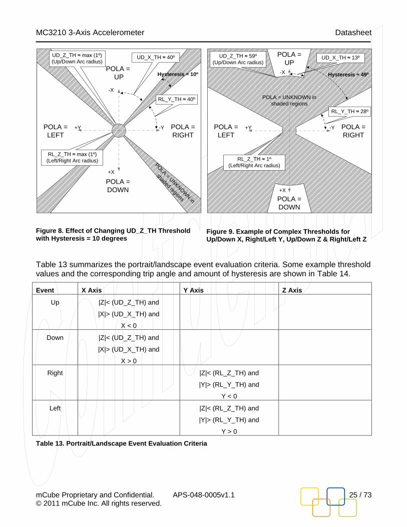
The Z threshold for each direction can also be adjusted, as shown in Figure 8. This has the effect of altering the angle relative to the Z axis which causes the orientation state to change.
Figure 9 shows an example of setting the UD_Z_TH and RL_Z_TH registers to different values, as well as setting the UD_X_TH and RL_Y_TH registers to different values. However for most applications the same value should be written to both registers in both cases.
MC3210 3-Axis Accelerometer Datasheet
mCube Proprietary and Confidential. APS-048-0005v1.1 25 / 73 © 2011 mCube Inc. All rights reserved.
POLA
= UNKNOW
N in
shaded regions
UD_X_TH ≈ 40º
RL_Y_TH ≈ 40º
RL_Z_TH ≈ max (1º)
(Left/Right Arc radius)
Hysteresis ≈ 10º
UD_Z_TH ≈ max (1º)
(Up/Down Arc radius)
-X
-Y+Y
+X
POLA =
LEFT
POLA =
RIGHT
POLA =
DOWN
POLA =
UP
Figure 8. Effect of Changing UD_Z_TH Threshold with Hysteresis = 10 degrees
POLA = UNKNOWN in
shaded regions
-X
UD_X_TH ≈ 13º
+X
POLA =
DOWN
POLA =
UP
RL_Y_TH ≈ 28º
RL_Z_TH ≈ 1º
(Left/Right Arc radius)
Hysteresis ≈ 49º
UD_Z_TH ≈ 59º
(Up/Down Arc radius)
-Y+YPOLA =
LEFT
POLA =
RIGHT
Figure 9. Example of Complex Thresholds for Up/Down X, Right/Left Y, Up/Down Z & Right/Left Z
Table 13 summarizes the portrait/landscape event evaluation criteria. Some example threshold values and the corresponding trip angle and amount of hysteresis are shown in Table 14.
Event X Axis Y Axis Z Axis
Up |Z|< (UD_Z_TH) and
|X|> (UD_X_TH) and
X < 0
Down |Z|< (UD_Z_TH) and
|X|> (UD_X_TH) and
X > 0
Right |Z|< (RL_Z_TH) and
|Y|> (RL_Y_TH) and
Y < 0
Left |Z|< (RL_Z_TH) and
|Y|> (RL_Y_TH) and
Y > 0
Table 13. Portrait/Landscape Event Evaluation Criteria

MC3210 3-Axis Accelerometer Datasheet
mCube Proprietary and Confidential. APS-048-0005v1.1 26 / 73 © 2011 mCube Inc. All rights reserved.
Registers UD_X_TH or RL_Y_TH
Threshold Value
Trip Angle
(approx. degrees)
Resulting Hysteresis
(approx. degrees)
Corresponding g Value
(approximate)
0x00 45 0 0.72
0x10 43 4 0.68
0x20 41 8 0.66
0x30 39 12 0.63
0x40 37 16 0.61
0x50 36 20 0.58
0x60 34 24 0.55
… … … …
0xFF 15 64 0.26
Table 14. Some Approximate X and Y-axis Portrait/Landscape Evaluation Angles and Values
Registers UD_Z_TH or RL_Z_TH
Threshold Value
Trip Angle
(approx. degrees)
Corresponding
g Value (approximate)
0x80 67 0.43
0x90 64 0.47
… … …
0xE0 48 0.71
0xF0 45 0.75
0x00 40 0.80
0x10 36 0.85
0x20 32 0.89
… … …
0x70 9 1.13
0x7F 3 Max (~0.17)*
Table 15. Some Approximate Z-axis Portrait/Landscape Evaluation Angles and Values
NOTE*: Max values >1.0g are possible, to cover offset variations.
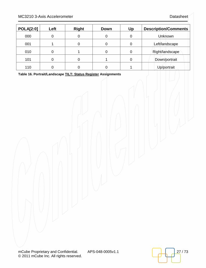
Table 16 shows the orientation event conditions for the portrait/landscape detection hardware.
MC3210 3-Axis Accelerometer Datasheet
mCube Proprietary and Confidential. APS-048-0005v1.1 27 / 73 © 2011 mCube Inc. All rights reserved.
POLA[2:0] Left Right Down Up Description/Comments
000 0 0 0 0 Unknown
001 1 0 0 0 Left/landscape
010 0 1 0 0 Right/landscape
101 0 0 1 0 Down/portrait
110 0 0 0 1 Up/portrait
Table 16. Portrait/Landscape TILT: Status Register Assignments
MC3210 3-Axis Accelerometer Datasheet
mCube Proprietary and Confidential. APS-048-0005v1.1 28 / 73 © 2011 mCube Inc. All rights reserved.
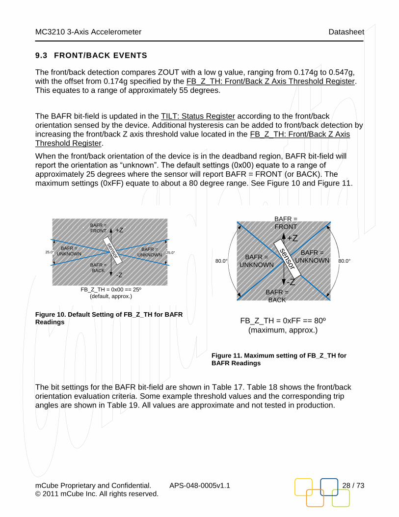
9.3 FRONT/BACK EVENTS
The front/back detection compares ZOUT with a low g value, ranging from 0.174g to 0.547g, with the offset from 0.174g specified by the FB_Z_TH: Front/Back Z Axis Threshold Register. This equates to a range of approximately 55 degrees.
The BAFR bit-field is updated in the TILT: Status Register according to the front/back orientation sensed by the device. Additional hysteresis can be added to front/back detection by increasing the front/back Z axis threshold value located in the FB_Z_TH: Front/Back Z Axis Threshold Register.
When the front/back orientation of the device is in the deadband region, BAFR bit-field will report the orientation as “unknown”. The default settings (0x00) equate to a range of approximately 25 degrees where the sensor will report BAFR = FRONT (or BACK). The maximum settings (0xFF) equate to about a 80 degree range. See Figure 10 and Figure 11.
25.0° 25.0°
-Z
+Z
senso
rFB_Z_TH = 0x00 == 25º
(default, approx.)
BAFR =
FRONT
BAFR =
BACK
BAFR =
UNKNOWN
BAFR =
UNKNOWN
Figure 10. Default Setting of FB_Z_TH for BAFR Readings
FB_Z_TH = 0xFF == 80º
(maximum, approx.)
80.0°80.0°
+Z
-Z
senso
r
BAFR =
UNKNOWN
BAFR =
UNKNOWN
BAFR =
FRONT
BAFR =
BACK
Figure 11. Maximum setting of FB_Z_TH for BAFR Readings
The bit settings for the BAFR bit-field are shown in Table 17. Table 18 shows the front/back orientation evaluation criteria. Some example threshold values and the corresponding trip angles are shown in Table 19. All values are approximate and not tested in production.

MC3210 3-Axis Accelerometer Datasheet
mCube Proprietary and Confidential. APS-048-0005v1.1 29 / 73 © 2011 mCube Inc. All rights reserved.
BAFR[1:0] Status
00 Unknown condition of front or back
01 Front: Device is in orientation e. in Figure 18
10 Back: Device is in orientation f. in Figure 18
11 Reserved
Table 17. BAFR Bit Assignments in the TILT: Status Register
Event X Axis Y Axis Z Axis
Front Z > FB_Z_TH
Back Z < -1 * FB_Z_TH
Table 18. Front/Back Event Evaluation
Threshold Value
FB_Z_TH Trip Angle
(approx. degrees)
0x00 25
0x10 28
0x20 32
0x30 35
0x40 39
0x50 42
0x60 46
0x70 49
… …
0xFF 80
Table 19. Approximate Front/Back Evaluation Angles and Values

MC3210 3-Axis Accelerometer Datasheet
mCube Proprietary and Confidential. APS-048-0005v1.1 30 / 73 © 2011 mCube Inc. All rights reserved.
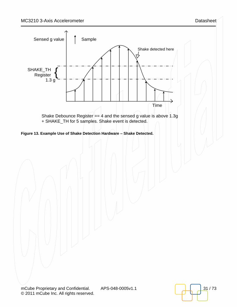
9.4 SHAKE DETECTION
The threshold for detecting a shake event can be set to a range of values around a 1.3g baseline. The shake threshold can range from 0.925g to 1.672g. The value is a signed, 2‟s complement number. Resolution is approximately 2.9mg/bit.
A shake event will be triggered when high-g values are sensed for a sufficient number of samples.
SHDB: Shake Debounce Register can be set to count from 1 to 63 events before setting the SHAKED bit in the TILT: Status Register. Higher values yield longer evaluation periods. See Figure 12 and Figure 13.
Shake detection can be any combination of axes. To enable detection even when not using interrupts, set the corresponding SHINTX, SHINTY, or SHINTZ bit-fields in the INTEN: Interrupt Enable Register.
Event X Axis Y Axis Z Axis
Shake |X| > +1.3g ± Threshold or |Y| > +1.3g ±
Threshold or |Z| > +1.3g± Threshold
Table 20. SHAKE Event Evaluation (Baseline + Offset)
SampleSensed g value
Time
Shake Debounce Register == 4 but the sensed g value is above 1.3g
+ SHAKE_TH for only 3 samples. Shake event is not detected.
1.3 g
SHAKE_TH
Register
Shake detect is reset here
Figure 12. Example Use of Shake Detection Hardware – Shake Not Detected
MC3210 3-Axis Accelerometer Datasheet
mCube Proprietary and Confidential. APS-048-0005v1.1 31 / 73 © 2011 mCube Inc. All rights reserved.
Sensed g value
SHAKE_TH
Register
Time
Sample
Shake Debounce Register == 4 and the sensed g value is above 1.3g
+ SHAKE_TH for 5 samples. Shake event is detected.
1.3 g
Shake detected here
Figure 13. Example Use of Shake Detection Hardware – Shake Detected.
MC3210 3-Axis Accelerometer Datasheet
mCube Proprietary and Confidential. APS-048-0005v1.1 32 / 73 © 2011 mCube Inc. All rights reserved.
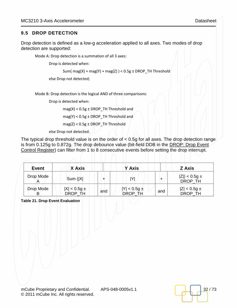
9.5 DROP DETECTION
Drop detection is defined as a low-g acceleration applied to all axes. Two modes of drop detection are supported:
Mode A: Drop detection is a summation of all 3 axes:
Drop is detected when:
Sum( mag(X) + mag(Y) + mag(Z) ) < 0.5g ± DROP_TH Threshold
else Drop not detected;
Mode B: Drop detection is the logical AND of three comparisons:
Drop is detected when:
mag(X) < 0.5g ± DROP_TH Threshold and
mag(Y) < 0.5g ± DROP_TH Threshold and
mag(Z) < 0.5g ± DROP_TH Threshold
else Drop not detected.
The typical drop threshold value is on the order of < 0.5g for all axes. The drop detection range is from 0.125g to 0.872g. The drop debounce value (bit-field DDB in the DROP: Drop Event Control Register) can filter from 1 to 8 consecutive events before setting the drop interrupt.
Event X Axis Y Axis Z Axis
Drop Mode A
Sum (|X| + |Y| + |Z|) < 0.5g ± DROP_TH
Drop Mode B
|X| < 0.5g ± DROP_TH
and |Y| < 0.5g ± DROP_TH
and |Z| < 0.5g ± DROP_TH
Table 21. Drop Event Evaluation

MC3210 3-Axis Accelerometer Datasheet
mCube Proprietary and Confidential. APS-048-0005v1.1 33 / 73 © 2011 mCube Inc. All rights reserved.
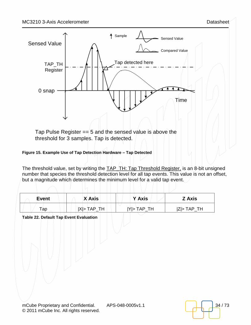
9.6 TAP DETECTION
On-chip tap detection hardware allows the device to detect user events such as on-screen button presses. Tap detection can be enabled or disabled on each axis via the TAPEN: Tap Detection Enable Register.
To detect fast, impulse events like a tap, the TAPP: Tap Pulse Register should be written with a tap pulse parameter that sets the maximum number of sample periods that a TAPD event may exceed the threshold before it is ignored by the detection logic. Sensed values that are above the threshold for long periods of time typically do not correspond to tap events.
For example, setting the pulse value to 5 requires that the tap impulse exceed the threshold for at least 1 sample period and up to 5 sample periods. The tap detection hardware is rearmed after the sensed value is below the threshold. See the example in Figure 14 and Figure 15.
Sensed Value
TAP_TH
Register
Time
Sample
Tap Pulse Register == 5 but the sensed value is above the
threshold for 10 samples. No tap is detected.
Tap detect is reset here
(6th sample)
Tap detect is
rearmed here
0 snap
Figure 14. Example Use of Tap Detection Hardware – No Tap Detected
MC3210 3-Axis Accelerometer Datasheet
mCube Proprietary and Confidential. APS-048-0005v1.1 34 / 73 © 2011 mCube Inc. All rights reserved.
Sample
Sensed Value
TAP_TH
Register
Time
Tap Pulse Register == 5 and the sensed value is above the
threshold for 3 samples. Tap is detected.
Tap detected here
0 snap
Compared Value
Sensed Value
Figure 15. Example Use of Tap Detection Hardware – Tap Detected
The threshold value, set by writing the TAP_TH: Tap Threshold Register, is an 8-bit unsigned number that species the threshold detection level for all tap events. This value is not an offset, but a magnitude which determines the minimum level for a valid tap event.
Event X Axis Y Axis Z Axis
Tap |X|> TAP_TH |Y|> TAP_TH |Z|> TAP_TH
Table 22. Default Tap Event Evaluation
MC3210 3-Axis Accelerometer Datasheet
mCube Proprietary and Confidential. APS-048-0005v1.1 35 / 73 © 2011 mCube Inc. All rights reserved.
9.7 CONTINUOUS SAMPLING
The device has the ability to read all sampled readings in a continuous sampling fashion. The device always updates the XOUT_EX, YOUT_EX, and ZOUT_EX registers at 1024 samples/second.
An optional interrupt can be generated each time the sample registers have been updated (GINT interrupt bit in the INTEN: Interrupt Enable Register). See Sections 8.3 and 11.11 for GINT operation and options.

MC3210 3-Axis Accelerometer Datasheet
mCube Proprietary and Confidential. APS-048-0005v1.1 36 / 73 © 2011 mCube Inc. All rights reserved.
10 I2C INTERFACE
10.1 PHYSICAL INTERFACE
The I2C slave interface operates at a maximum speed of 400 kHz. The SDA (data) is an open-drain, bi-directional pin and the SCL (clock) is an input pin.
The device always operates as an I2C slave.
An I2C master initiates all communication and data transfers and generates the SCL clock that synchronizes the data transfer. The I2C device address is 0x4c (8-bit address 0x98).
The I2C interface remains active as long as power is applied to the DVDD and AVDD pins. In STANDBY state the device responds to I2C read and write cycles, but interrupts cannot be serviced or cleared. All registers can be written in the STANDBY state, but in WAKE only the MODE: Register can be modified.
Internally, the registers which are used to store samples are clocked by the sample clock gated by I2C activity. Therefore, in order to allow the device to collect and present samples in the sample registers at least one I2C STOP condition must be present between samples.
Refer to the I2C specification for a detailed discussion of the protocol. Per I2C requirements, SDA is an open drain, bi-directional pin. SCL and SDA each require an external pull-up resistor, typically 4.7kΩ. Refer also to Figure 3. Typical Application Circuit.
10.2 TIMING
See Section 4.3.3 I2C Timing Characteristics for I2C timing requirements.
10.3 I2C MESSAGE FORMAT
The device uses the following general format for writing to the internal registers. The I2C master generates a START condition, and then supplies the device ID, 0x4C or 1001100. The 8th bit is the R/W# flag (write cycle = 0). The device pulls SDA low during the 9th clock cycle indicating a positive ACK. This means, from an 8-bit point of view of an external I2C master, writes should be written to address 0x98 and reads will occur by reading address 0x99.
The second byte is the 8-bit register address of the device to access, and the last byte is the data to write.
1 0 0 1 01 0 0
ACK
R7 R6 R5 R4 R1R3 R2 R0 D7 D6 D5 D4 D1D4 D2 D0 PS
ACK ACK
START Device ID (4C) R/W#
ACK/NAK
Register Address Register Data to Write Stop
ACK/NAK ACK/NAK
I2C Master
(To Sensor)
I2C Slave
(From Sensor)
Figure 16. I2C Message Format, Write Cycle, Single Register Write
MC3210 3-Axis Accelerometer Datasheet
mCube Proprietary and Confidential. APS-048-0005v1.1 37 / 73 © 2011 mCube Inc. All rights reserved.
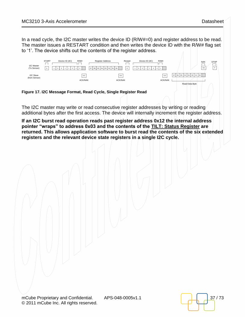
In a read cycle, the I2C master writes the device ID (R/W#=0) and register address to be read. The master issues a RESTART condition and then writes the device ID with the R/W# flag set to „1‟. The device shifts out the contents of the register address.
1 0 0 1 01 0 0
ACK
R7 R6 R5 R4 R1R3 R2 R0 RS
ACK
I2C Master
(To Sensor)
I2C Slave
(from Sensor)
START Device ID (4C) R/W#
ACK/NAK
Register Address Restart
ACK/NAK
D7 D6 D5 D4 D1D3 D2 D0
NAK
Read Data Byte
NAK
1 0 0 1 01 0 1
ACK
Device ID (4C) R/W#
ACK/NAK
P
STOP
Figure 17. I2C Message Format, Read Cycle, Single Register Read
The I2C master may write or read consecutive register addresses by writing or reading additional bytes after the first access. The device will internally increment the register address.
If an I2C burst read operation reads past register address 0x12 the internal address pointer “wraps” to address 0x03 and the contents of the TILT: Status Register are returned. This allows application software to burst read the contents of the six extended registers and the relevant device state registers in a single I2C cycle.

MC3210 3-Axis Accelerometer Datasheet
mCube Proprietary and Confidential. APS-048-0005v1.1 38 / 73 © 2011 mCube Inc. All rights reserved.
11 REGISTER INTERFACE
The device has a simple register interface which allows a MCU or I2C master to configure and monitor all aspects of the device. This section lists an overview of user programmable registers. By convention, Bit 0 is the least significant bit (LSB) of a byte register.
Two registers are needed in order to contain each sample, the XOUT_EX, YOUT_EX & ZOUT_EX: X, Y, Z-Axis Extended Accelerometer Registers. The least significant byte is located in the register with a lower address (e.g. XOUT_EX_L), followed by the most significant byte in the next higher address (e.g. XOUT_EX_H).

MC3210 3-Axis Accelerometer Datasheet
mCube Proprietary and Confidential. APS-048-0005v1.1 39 / 73 © 2011 mCube Inc. All rights reserved.
11.1 REGISTER SUMMARY
Addr Name Description Bit 7 Bit 6 Bit 5 Bit 4 Bit 3 Bit 2 Bit 1 Bit 0 POR
Value
R/
W5
0x00-0x02 RESERVED6
0x03 TILT Tilt Status Register SHAKED DROPD TAPD POLA
[2] POLA
[1] POLA
[0] BAFR
[1] BAFR
[0] 0x00 R
0x04 OPSTAT Operational State
Status Register
OTPA 0 OTPE 0 0 0 OPSTAT
[1] OPSTAT
[0] 0x03 R
0x05 RESERVED6
0x06 INTEN Interrupt Enable
Register
SHINTX SHINTY SHINTZ GINT ASINT TINT PLINT FBINT 0x00 W
0x07 MODE Mode Register IAH IPP Resv8 Resv
8 Resv
8 0
7
OPCON [1]
OPCON [0]
0x03 W
0x08 RESERVED6
0x09 TAPEN Tap Detection
Enable Register
ZDA YDA XDA Resv8 Resv
8 Resv
8 Resv
8 Resv
8 0x00 W
0x0A TAPP Tap Pulse Register
Resv8 Resv
8 Resv
8 Resv
8
TAPP [3]
TAPP [2]
TAPP [1]
TAPP [0]
0x00 W
0x0B DROP Drop Event Control
Register
DROP_ MODE
DINT Resv8 Resv
8 Resv
8
DROP_ DB[2]
DROP_ DB[1]
DROP_ DB[0]
0x00 W
0x0C SHDB Shake Debounce
Register
Resv8 Resv
8
SHDB [5]
SHDB [4]
SHDB [3]
SHDB [2]
SHDB [1]
SHDB [0]
0x00 W
0x0D XOUT _EX_L
XOUT Extended Register
XOUT _EX[7]
XOUT _EX[6]
XOUT _EX[5]
XOUT _EX[4]
XOUT _EX[3]
XOUT _EX[2]
XOUT _EX[1]
XOUT _EX[0]
0x00 R
0x0E XOUT _EX_H
XOUT Extended Register
XOUT _EX[15]
XOUT _EX[14]
XOUT _EX[13]
XOUT _EX[12]
XOUT _EX[11]
XOUT _EX[10]
XOUT _EX[9]
XOUT _EX[8]
0x00 R
0x0F YOUT _EX_L
YOUT Extended Register
YOUT _EX[7]
YOUT _EX[6]
YOUT _EX[5]
YOUT _EX[4]
YOUT _EX[3]
YOUT _EX[2]
YOUT _EX[1]
YOUT _EX[0] 0x00 R
0x10 YOUT _EX_H
YOUT Extended Register
YOUT _EX[15]
YOUT _EX[14]
YOUT _EX[13]
YOUT _EX[12]
YOUT _EX[11]
YOUT _EX[10]
YOUT _EX[9]
YOUT _EX[8] 0x00 R
0x11 ZOUT _EX_L
ZOUT Extended Register
ZOUT _EX[7]
ZOUT _EX[6]
ZOUT _EX[5]
ZOUT _EX[4]
ZOUT _EX[3]
ZOUT _EX[2]
ZOUT _EX[1]
ZOUT _EX[0] 0x00 R
0x12 ZOUT _EX_H
ZOUT Extended Register
ZOUT _EX[15]
ZOUT _EX[14]
ZOUT _EX[13]
ZOUT _EX[12]
ZOUT _EX[11]
ZOUT _EX[10]
ZOUT _EX[9]
ZOUT _EX[8] 0x00 R
0x13-0x17 RESERVED6
0x18 CHIPID Chip ID Register 0 0 0 0 0 0 0 1 0x01 R
0x19-0x1F RESERVED6
0x20 OUTCFG Output
Configuration Register
IRATE LPF [2]
LPF [1]
LPF [0]
HIRES [1]
HIRES [0]
19 1
9 0x03 W
0x21 XOFFL X-Offset
LSB Register
XOFF[7] XOFF[6] XOFF[5] XOFF[4] XOFF[3] XOFF[2] XOFF[1] XOFF[0] Per chip W
5 ‘R’ registers are read-only, via external I2C access. ‘W’ registers are read-write, via external I2C access.
6 Registers designated as ‘RESERVED’ should not be accessed by software.
7 Software must always write a zero ‘0’ to this bit.
8 Bits designated as ‘Resv’ are reserved for future use.
9 Software must always write a one ‘1’ to this bit.

MC3210 3-Axis Accelerometer Datasheet
mCube Proprietary and Confidential. APS-048-0005v1.1 40 / 73 © 2011 mCube Inc. All rights reserved.
Addr Name Description Bit 7 Bit 6 Bit 5 Bit 4 Bit 3 Bit 2 Bit 1 Bit 0 POR
Value
R/
W5
0x22 XOFFH X-Offset
MSB Register
XGAIN[8] Resv8 XOFF[13] XOFF[12] XOFF[11] XOFF[10] XOFF[9] XOFF[8] Per chip W
0x23 YOFFL Y-Offset
LSB Register
YOFF[7] YOFF[6] YOFF[5] YOFF[4] YOFF[3] YOFF[2] YOFF[1] YOFF[0] Per chip W
0x24 YOFFH Y-Offset
MSB Register
YGAIN[8] Resv8 YOFF[13] YOFF[12] YOFF[11] YOFF[10] YOFF[9] YOFF[8] Per chip W
0x25 ZOFFL Z-Offset
LSB Register
ZOFF[7] ZOFF[6] ZOFF[5] ZOFF[4] ZOFF[3] ZOFF[2] ZOFF[1] ZOFF[0] Per chip W
0x26 ZOFFH Z-Offset
MSB Register
ZGAIN[8] Resv8 ZOFF[13] ZOFF[12] ZOFF[11] ZOFF[10] ZOFF[9] ZOFF[8] Per chip W
0x27 XGAIN X Gain Register XGAIN[7] XGAIN[6] XGAIN[5] XGAIN[4] XGAIN[3] XGAIN[2] XGAIN[1] XGAIN[0] Per chip W
0x28 YGAIN Y Gain Register YGAIN[7] YGAIN[6] YGAIN[5] YGAIN[4] YGAIN[3] YGAIN[2] YGAIN[1] YGAIN[0] Per chip W
0x29 ZGAIN Z Gain Register ZGAIN[7] ZGAIN[6] ZGAIN[5] ZGAIN[4] ZGAIN[3] ZGAIN[2] ZGAIN[1] ZGAIN[0] Per chip W
0x2A RESERVED6
0x2B SHAKE
_TH Shake
Threshold Register
SHAKE _TH[7]
SHAKE _TH[6]
SHAKE _TH[5]
SHAKE _TH[4]
SHAKE _TH[3]
SHAKE _TH[2]
SHAKE _TH[1]
SHAKE _TH[0]
0x00 W
0x2C UD_Z _TH
Up/Down Z Threshold Register
UD_Z _TH[7]
UD_Z _TH[6]
UD_Z _TH[5]
UD_Z _TH[4]
UD_Z _TH[3]
UD_Z _TH[2]
UD_Z _TH[1]
UD_Z _TH[0]
0x00 W
0x2D UD_X _TH
Up/Down X Threshold Register
UD_X _TH[7]
UD_X _TH[6]
UD_X _TH[5]
UD_X _TH[4]
UD_X _TH[3]
UD_X _TH[2]
UD_X _TH[1]
UD_X _TH[0]
0x00 W
0x2E RL_Z _TH
Right/Left Z Threshold Register
RL_Z _TH[7]
RL_Z _TH[6]
RL_Z _TH[5]
RL_Z _TH[4]
RL_Z _TH[3]
RL_Z _TH[2]
RL_Z _TH[1]
RL_Z _TH[0]
0x00 W
0x2F RL_Y _TH
Right/Left Y Threshold Register
RL_Y _TH[7]
RL_Y _TH[6]
RL_Y _TH[5]
RL_Y _TH[4]
RL_Y _TH[3]
RL_Y _TH[2]
RL_Y _TH[1]
RL_Y _TH[0]
0x00 W
0x30 FB_Z _TH
Front/Back Z Threshold Register
FB_Z _TH[7]
FB_Z _TH[6]
FB_Z _TH[5]
FB_Z _TH[4]
FB_Z _TH[3]
FB_Z _TH[2]
FB_Z _TH[1]
FB_Z _TH[0]
0x00 W
0x31 DROP _TH
Drop Threshold Register
DROP _TH[7]
DROP _TH[6]
DROP _TH[5]
DROP _TH[4]
DROP _TH[3]
DROP _TH[2]
DROP _TH[1]
DROP _TH[0]
0x00 W
0x32 TAP _TH
Tap Threshold Register
TAP _TH[7]
TAP _TH[6]
TAP _TH[5]
TAP _TH[4]
TAP _TH[3]
TAP _TH[2]
TAP _TH[1]
TAP _TH[0]
0x00 W
0x33 to 0x3A RESERVED6
0x3B PCODE Product Code 1 0 0 1 0 0 0 0 0x90 R
0x3C to 0x3F RESERVED6
Table 23. Register Summary10
10
No registers are updated with new event status or samples while a I2C cycle is in process.
MC3210 3-Axis Accelerometer Datasheet
mCube Proprietary and Confidential. APS-048-0005v1.1 41 / 73 © 2011 mCube Inc. All rights reserved.
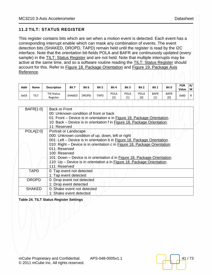
11.2 TILT: STATUS REGISTER
This register contains bits which are set when a motion event is detected. Each event has a corresponding interrupt enable which can mask any combination of events. The event detection bits (SHAKED, DROPD, TAPD) remain held until the register is read by the I2C interface. Note that the orientation bit-fields POLA and BAFR are continuously updated (every sample) in the TILT: Status Register and are not held. Note that multiple interrupts may be active at the same time, and so a software routine reading the TILT: Status Register should account for this. Refer to Figure 18. Package Orientation and Figure 19. Package Axis Reference.
Addr Name Description Bit 7 Bit 6 Bit 5 Bit 4 Bit 3 Bit 2 Bit 1 Bit 0 POR
Value R/W
0x03 TILT Tilt Status Register
SHAKED DROPD TAPD POLA
[2] POLA
[1] POLA
[0] BAFR
[1] BAFR
[0] 0x00 R
BAFR[1:0] Back or Front 00: Unknown condition of front or back 01: Front – Device is in orientation e in Figure 18. Package Orientation. 10: Back – Device is in orientation f in Figure 18. Package Orientation. 11: Reserved
POLA[2:0] Portrait or Landscape 000: Unknown condition of up, down, left or right 001: Left – Device is in orientation b in Figure 18. Package Orientation. 010: Right – Device is in orientation c in Figure 18. Package Orientation. 011: Reserved 100: Reserved 101: Down – Device is in orientation d in Figure 18. Package Orientation. 110: Up – Device is in orientation a in Figure 18. Package Orientation. 111: Reserved
TAPD 0: Tap event not detected 1: Tap event detected
DROPD 0: Drop event not detected 1: Drop event detected
SHAKED 0: Shake event not detected 1: Shake event detected
Table 24. TILT Status Register Settings
MC3210 3-Axis Accelerometer Datasheet
mCube Proprietary and Confidential. APS-048-0005v1.1 42 / 73 © 2011 mCube Inc. All rights reserved.
Direction of
Earth gravity
acceleration
XOUT = +1g
YOUT = 0g
ZOUT = 0g
XOUT = -1g
YOUT = 0g
ZOUT = 0g
XOUT = 0g
YOUT = +1g
ZOUT = 0g
XOUT = 0g
YOUT = -1g
ZOUT = 0g
XOUT = 0g
YOUT = 0g
ZOUT = +1g
XOUT = 0g
YOUT = 0g
ZOUT = -1g
Top View
Side ViewPin 1
Top
a.
b. c.
d.
e.
f.
TILT = LEFT TILT = RIGHT
TILT = UP
TILT = DOWN
TILT = FRONT
TILT = BACK
Figure 18. Package Orientation
+X
-X-Y
+Y
+Z
-Z
Figure 19. Package Axis Reference
MC3210 3-Axis Accelerometer Datasheet
mCube Proprietary and Confidential. APS-048-0005v1.1 43 / 73 © 2011 mCube Inc. All rights reserved.
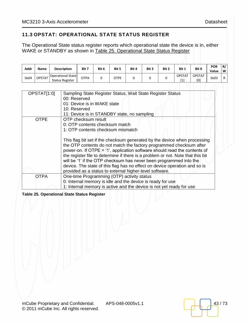
11.3 OPSTAT: OPERATIONAL STATE STATUS REGISTER
The Operational State status register reports which operational state the device is in, either WAKE or STANDBY as shown in Table 25. Operational State Status Register
Addr Name Description Bit 7 Bit 6 Bit 5 Bit 4 Bit 3 Bit 2 Bit 1 Bit 0 POR
Value R/W
0x04 OPSTAT Operational State
Status Register OTPA 0 OTPE 0 0 0
OPSTAT [1]
OPSTAT [0]
0x03 R
OPSTAT[1:0] Sampling State Register Status, Wait State Register Status 00: Reserved 01: Device is in WAKE state 10: Reserved 11: Device is in STANDBY state, no sampling
OTPE OTP checksum result 0: OTP contents checksum match 1: OTP contents checksum mismatch This flag bit set if the checksum generated by the device when processing the OTP contents do not match the factory programmed checksum after power-on. If OTPE = „1‟, application software should read the contents of the register file to determine if there is a problem or not. Note that this bit will be „1‟ if the OTP checksum has never been programmed into the device. The state of this flag has no effect on device operation and so is provided as a status to external higher-level software.
OTPA One-time Programming (OTP) activity status 0: Internal memory is idle and the device is ready for use 1: Internal memory is active and the device is not yet ready for use
Table 25. Operational State Status Register

MC3210 3-Axis Accelerometer Datasheet
mCube Proprietary and Confidential. APS-048-0005v1.1 44 / 73 © 2011 mCube Inc. All rights reserved.
11.4 INTEN: INTERRUPT ENABLE REGISTER
The interrupt enable register enables or disables interrupts on various motion events. If the corresponding interrupt enable bit is set, a matching event will generate an interrupt transition on the external interrupt pin, INTN. To enable the drop interrupt, set the DINT control bit in the DROP: Drop Event Control Register.
When an interrupt is triggered, the first I2C access to the device will clear the external interrupt pin, but the condition (TAPD, SHAKED, DROPD) that generated the interrupt will remain held in the TILT: Status Register until it is read. Note that the orientation bit-fields POLA and BAFR are continuously updated (every sample) in the TILT: Status Register and are not held.
Addr Name Description Bit 7 Bit 6 Bit 5 Bit 4 Bit 3 Bit 2 Bit 1 Bit 0 POR
Value R/W
0x06 INTEN Interrupt Enable
Register SHINTX SHINTY SHINTZ GINT Resv TINT PLINT FBINT 0x00 W
FBINT Front / Back Interrupt 0: Disable interrupt on front/back position change 1: Enable interrupt on front/back position change
PLINT Portrait / Landscape Interrupt 0: Disable interrupt on up/down/left/right position change 1: Enable interrupt on up/down/left/right position change
TINT Tap Interrupt 0: Disable interrupt on tap detection 1: Enable interrupt on tap detection
Reserved Reserved
GINT Generate Interrupt 0: Disable automatic interrupt after each measurement 1: Enable automatic interrupt after each measurement is updated in XOUT, YOUT, or ZOUT. The interrupt occurs for each measurement, not value change. See Section 8.3.
SHINTX Shake Interrupt, X-axis 0: Disable X-axis interrupt, SHAKED is not set in TILT: Status Register upon event 1 : Enable X-axis interrupt, SHAKED is set in TILT: Status Register upon event
SHINTY Shake Interrupt, Y-axis 0: Disable Y-axis interrupt, SHAKED bit is not set in TILT: Status Register upon event 1 : Enable Y-axis interrupt, SHAKED bit is set in TILT: Status Register upon event
SHINTZ Shake Interrupt, Z-axis 0: Disable Z-axis interrupt, SHAKED bit is not set in TILT: Status Register upon event 1 : Enable Z-axis interrupt, SHAKED bit is set in TILT: Status Register upon event
Table 26. Interrupt Enable Register Settings
MC3210 3-Axis Accelerometer Datasheet
mCube Proprietary and Confidential. APS-048-0005v1.1 45 / 73 © 2011 mCube Inc. All rights reserved.
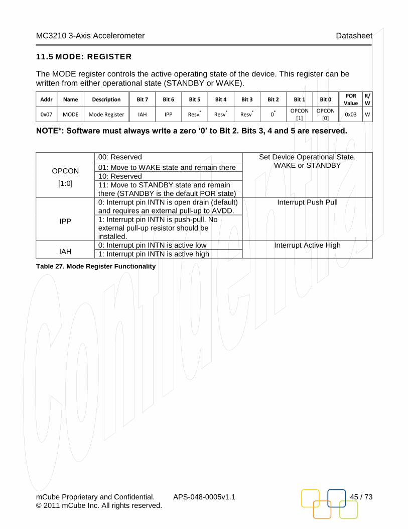
11.5 MODE: REGISTER
The MODE register controls the active operating state of the device. This register can be written from either operational state (STANDBY or WAKE).
Addr Name Description Bit 7 Bit 6 Bit 5 Bit 4 Bit 3 Bit 2 Bit 1 Bit 0 POR
Value R/W
0x07 MODE Mode Register IAH IPP Resv* Resv
* Resv
* 0
*
OPCON [1]
OPCON [0]
0x03 W
NOTE*: Software must always write a zero „0‟ to Bit 2. Bits 3, 4 and 5 are reserved.
OPCON
[1:0]
00: Reserved Set Device Operational State. WAKE or STANDBY 01: Move to WAKE state and remain there
10: Reserved
11: Move to STANDBY state and remain there (STANDBY is the default POR state)
IPP
0: Interrupt pin INTN is open drain (default) and requires an external pull-up to AVDD.
Interrupt Push Pull
1: Interrupt pin INTN is push-pull. No external pull-up resistor should be installed.
IAH 0: Interrupt pin INTN is active low Interrupt Active High
1: Interrupt pin INTN is active high
Table 27. Mode Register Functionality

MC3210 3-Axis Accelerometer Datasheet
mCube Proprietary and Confidential. APS-048-0005v1.1 46 / 73 © 2011 mCube Inc. All rights reserved.
11.6 TAPEN: TAP DETECTION ENABLE REGISTER
This register allows individual tap/pulse detection on each axis. Setting XDA, YDA, or ZDA adds the corresponding axis to tap event detection. See also Section 9.6 Tap Detection.
Addr Name Description Bit 7 Bit 6 Bit 5 Bit 4 Bit 3 Bit 2 Bit 1 Bit 0 POR
Value R/W
0x09 TAPEN Tap Detection
Enable Register ZDA YDA XDA Resv Resv Resv Resv Resv 0x00 W
XDA 0: Disable Tap detection on X-axis 1: Enable Tap detection on X-axis
YDA
0: Disable Tap detection on Y-axis 1: Enable Tap detection on Y-axis
ZDA 0: Disable Tap detection on Z-axis 1: Enable Tap detection on Z-axis
Table 28. TAPEN Register Settings
MC3210 3-Axis Accelerometer Datasheet
mCube Proprietary and Confidential. APS-048-0005v1.1 47 / 73 © 2011 mCube Inc. All rights reserved.
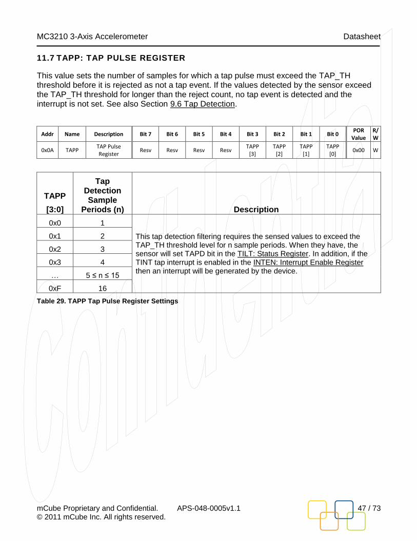
11.7 TAPP: TAP PULSE REGISTER
This value sets the number of samples for which a tap pulse must exceed the TAP_TH threshold before it is rejected as not a tap event. If the values detected by the sensor exceed the TAP_TH threshold for longer than the reject count, no tap event is detected and the interrupt is not set. See also Section 9.6 Tap Detection.
Addr Name Description Bit 7 Bit 6 Bit 5 Bit 4 Bit 3 Bit 2 Bit 1 Bit 0 POR
Value R/W
0x0A TAPP TAP Pulse Register
Resv Resv Resv Resv TAPP
[3] TAPP
[2] TAPP
[1] TAPP
[0] 0x00 W
TAPP
[3:0]
Tap Detection Sample
Periods (n) Description
0x0 1
This tap detection filtering requires the sensed values to exceed the TAP_TH threshold level for n sample periods. When they have, the sensor will set TAPD bit in the TILT: Status Register. In addition, if the TINT tap interrupt is enabled in the INTEN: Interrupt Enable Register then an interrupt will be generated by the device.
0x1 2
0x2 3
0x3 4
… 5 ≤ n ≤ 15
0xF 16
Table 29. TAPP Tap Pulse Register Settings

MC3210 3-Axis Accelerometer Datasheet
mCube Proprietary and Confidential. APS-048-0005v1.1 48 / 73 © 2011 mCube Inc. All rights reserved.
11.8 DROP: DROP EVENT CONTROL REGISTER
Addr Name Description Bit 7 Bit 6 Bit 5 Bit 4 Bit 3 Bit 2 Bit 1 Bit 0 POR
Value R/W
0x0B DROP Drop Event Control
Register DROP_ MODE
DINT Resv Resv Resv DROP_ DB[2]
DROP_ DB[1]
DROP_ DB[0]
0x00 W
DROP_DB[2:0] Drop Debounce 000: 1 drop event 001: 2 adjacent drop events 010: 3 adjacent drop events … : 4 ≤ n ≤ 7 adjacent drop events 111: 8 adjacent drop events
Drop event debounce value, the number of drop events detected must reach this count for the final event to be valid.
DINT Drop Interrupt 0: Disable drop event interrupt 1: Enable drop event interrupt
The DROPD bit in the TILT: Status Register will be set upon event occurrence regardless of this bit setting.
DROP_MODE Drop Mode 0: Mode A: Drop detection is a summation of all 3 axes: Drop is detected when: Sum( mag(X) + mag(Y) + mag(Z) ) < 0.5g ± DROP_TH Threshold else Drop not detected; 1: Mode B: Drop detection is the logical AND of three comparisons: Drop is detected when: mag(X) < 0.5g ± DROP_TH Threshold and mag(Y) < 0.5g ± DROP_TH Threshold and mag(Z) < 0.5g ± DROP_TH Threshold else Drop not detected.
Table 30. Drop Event Control Register Settings

MC3210 3-Axis Accelerometer Datasheet
mCube Proprietary and Confidential. APS-048-0005v1.1 49 / 73 © 2011 mCube Inc. All rights reserved.
11.9 SHDB: SHAKE DEBOUNCE REGISTER
The shake debounce register allows a 1 to 63 event count to be required before a valid shake event is detected or an interrupt is generated. The debounce value applies to all 3-axes.
Addr Name Description Bit 7 Bit 6 Bit 5 Bit 4 Bit 3 Bit 2 Bit 1 Bit 0 POR
Value R/W
0x0C SHDB Shake Debounce
Register Resv Resv
SHDB [5]
SHDB [4]
SHDB [3]
SHDB [2]
SHDB [1]
SHDB [0]
0x00 W
SHDB[5:0] Adjacent Shake
Events (n) Description
0x01 1 Shake detection debounce filtering requires n adjacent shake detection events in order to trigger a shake event and set the SHAKED bit in the TILT: Status Register. In addition, if the
SHINTX, SHINTY or SHINTZ bits are set in the INTEN: Interrupt Enable Register and that event occurs, then an interrupt will be
generated by the device.
0x02 2
0x03 3
…. 4 ≤ n ≤ 62
0x3F 63
Table 31. SH_DB Shake Debounce Register Settings
MC3210 3-Axis Accelerometer Datasheet
mCube Proprietary and Confidential. APS-048-0005v1.1 50 / 73 © 2011 mCube Inc. All rights reserved.
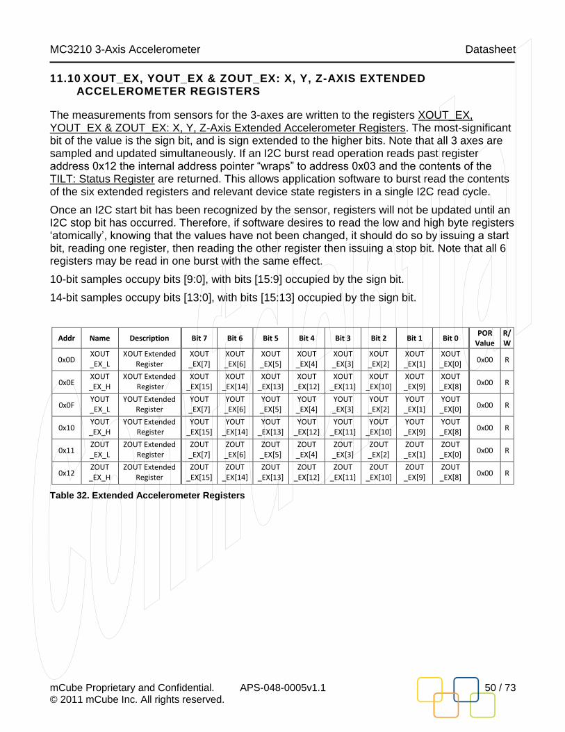
11.10 XOUT_EX, YOUT_EX & ZOUT_EX: X, Y, Z-AXIS EXTENDED ACCELEROMETER REGISTERS
The measurements from sensors for the 3-axes are written to the registers XOUT_EX, YOUT_EX & ZOUT_EX: X, Y, Z-Axis Extended Accelerometer Registers. The most-significant bit of the value is the sign bit, and is sign extended to the higher bits. Note that all 3 axes are sampled and updated simultaneously. If an I2C burst read operation reads past register address 0x12 the internal address pointer “wraps” to address 0x03 and the contents of the TILT: Status Register are returned. This allows application software to burst read the contents of the six extended registers and relevant device state registers in a single I2C read cycle.
Once an I2C start bit has been recognized by the sensor, registers will not be updated until an I2C stop bit has occurred. Therefore, if software desires to read the low and high byte registers „atomically‟, knowing that the values have not been changed, it should do so by issuing a start bit, reading one register, then reading the other register then issuing a stop bit. Note that all 6 registers may be read in one burst with the same effect.
10-bit samples occupy bits [9:0], with bits [15:9] occupied by the sign bit.
14-bit samples occupy bits [13:0], with bits [15:13] occupied by the sign bit.
Addr Name Description Bit 7 Bit 6 Bit 5 Bit 4 Bit 3 Bit 2 Bit 1 Bit 0 POR
Value R/W
0x0D XOUT _EX_L
XOUT Extended Register
XOUT _EX[7]
XOUT _EX[6]
XOUT _EX[5]
XOUT _EX[4]
XOUT _EX[3]
XOUT _EX[2]
XOUT _EX[1]
XOUT _EX[0]
0x00 R
0x0E XOUT _EX_H
XOUT Extended Register
XOUT _EX[15]
XOUT _EX[14]
XOUT _EX[13]
XOUT _EX[12]
XOUT _EX[11]
XOUT _EX[10]
XOUT _EX[9]
XOUT _EX[8] 0x00 R
0x0F YOUT _EX_L
YOUT Extended Register
YOUT _EX[7]
YOUT _EX[6]
YOUT _EX[5]
YOUT _EX[4]
YOUT _EX[3]
YOUT _EX[2]
YOUT _EX[1]
YOUT _EX[0] 0x00 R
0x10 YOUT _EX_H
YOUT Extended Register
YOUT _EX[15]
YOUT _EX[14]
YOUT _EX[13]
YOUT _EX[12]
YOUT _EX[11]
YOUT _EX[10]
YOUT _EX[9]
YOUT _EX[8] 0x00 R
0x11 ZOUT _EX_L
ZOUT Extended Register
ZOUT _EX[7]
ZOUT _EX[6]
ZOUT _EX[5]
ZOUT _EX[4]
ZOUT _EX[3]
ZOUT _EX[2]
ZOUT _EX[1]
ZOUT _EX[0] 0x00 R
0x12 ZOUT _EX_H
ZOUT Extended Register
ZOUT _EX[15]
ZOUT _EX[14]
ZOUT _EX[13]
ZOUT _EX[12]
ZOUT _EX[11]
ZOUT _EX[10]
ZOUT _EX[9]
ZOUT _EX[8]
0x00 R
Table 32. Extended Accelerometer Registers
MC3210 3-Axis Accelerometer Datasheet
mCube Proprietary and Confidential. APS-048-0005v1.1 51 / 73 © 2011 mCube Inc. All rights reserved.
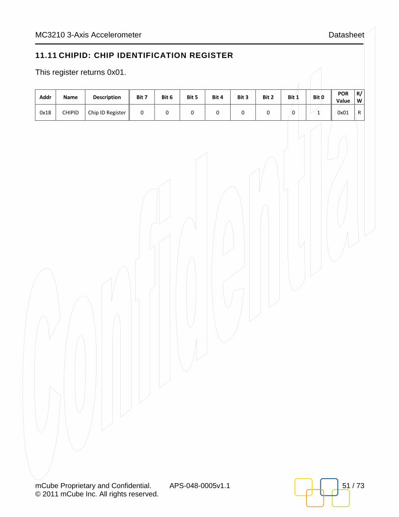
11.11 CHIPID: CHIP IDENTIFICATION REGISTER
This register returns 0x01.
Addr Name Description Bit 7 Bit 6 Bit 5 Bit 4 Bit 3 Bit 2 Bit 1 Bit 0 POR
Value R/W
0x18 CHIPID Chip ID Register 0 0 0 0 0 0 0 1 0x01 R
MC3210 3-Axis Accelerometer Datasheet
mCube Proprietary and Confidential. APS-048-0005v1.1 52 / 73 © 2011 mCube Inc. All rights reserved.
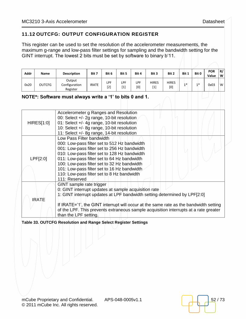
11.12 OUTCFG: OUTPUT CONFIGURATION REGISTER
This register can be used to set the resolution of the accelerometer measurements, the maximum g-range and low-pass filter settings for sampling and the bandwidth setting for the GINT interrupt. The lowest 2 bits must be set by software to binary b„11.
Addr Name Description Bit 7 Bit 6 Bit 5 Bit 4 Bit 3 Bit 2 Bit 1 Bit 0 POR
Value R/W
0x20 OUTCFG Output
Configuration Register
IRATE LPF [2]
LPF [1]
LPF [0]
HIRES [1]
HIRES [0]
1* 1* 0x03 W
NOTE*: Software must always write a „1‟ to bits 0 and 1.
HIRES[1:0]
Accelerometer g Ranges and Resolution 00: Select +/- 2g range, 10-bit resolution 01: Select +/- 4g range, 10-bit resolution 10: Select +/- 8g range, 10-bit resolution 11: Select +/- 8g range, 14-bit resolution
LPF[2:0]
Low Pass Filter bandwidth 000: Low-pass filter set to 512 Hz bandwidth 001: Low-pass filter set to 256 Hz bandwidth 010: Low-pass filter set to 128 Hz bandwidth 011: Low-pass filter set to 64 Hz bandwidth 100: Low-pass filter set to 32 Hz bandwidth 101: Low-pass filter set to 16 Hz bandwidth 110: Low-pass filter set to 8 Hz bandwidth 111: Reserved
IRATE
GINT sample rate trigger 0: GINT interrupt updates at sample acquisition rate 1: GINT interrupt updates at LPF bandwidth setting determined by LPF[2:0] If IRATE=‟1‟, the GINT interrupt will occur at the same rate as the bandwidth setting of the LPF. This prevents extraneous sample acquisition interrupts at a rate greater than the LPF setting.
Table 33. OUTCFG Resolution and Range Select Register Settings
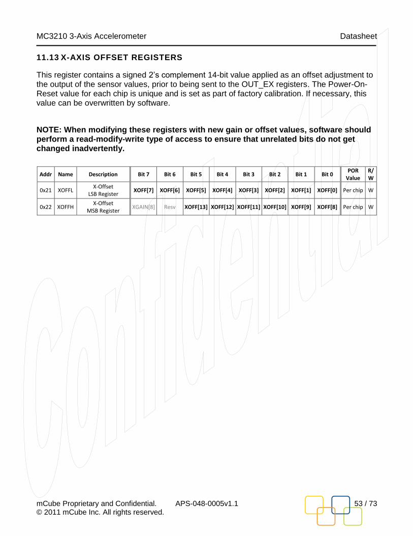
MC3210 3-Axis Accelerometer Datasheet
mCube Proprietary and Confidential. APS-048-0005v1.1 53 / 73 © 2011 mCube Inc. All rights reserved.
11.13 X-AXIS OFFSET REGISTERS
This register contains a signed 2‟s complement 14-bit value applied as an offset adjustment to the output of the sensor values, prior to being sent to the OUT_EX registers. The Power-On-Reset value for each chip is unique and is set as part of factory calibration. If necessary, this value can be overwritten by software.
NOTE: When modifying these registers with new gain or offset values, software should perform a read-modify-write type of access to ensure that unrelated bits do not get changed inadvertently.
Addr Name Description Bit 7 Bit 6 Bit 5 Bit 4 Bit 3 Bit 2 Bit 1 Bit 0 POR
Value R/W
0x21 XOFFL X-Offset
LSB Register XOFF[7] XOFF[6] XOFF[5] XOFF[4] XOFF[3] XOFF[2] XOFF[1] XOFF[0] Per chip W
0x22 XOFFH X-Offset
MSB Register XGAIN[8] Resv XOFF[13] XOFF[12] XOFF[11] XOFF[10] XOFF[9] XOFF[8] Per chip W

MC3210 3-Axis Accelerometer Datasheet
mCube Proprietary and Confidential. APS-048-0005v1.1 54 / 73 © 2011 mCube Inc. All rights reserved.
11.14 Y-AXIS OFFSET REGISTERS
This register contains a signed 2‟s complement 14-bit value applied as an offset adjustment to the output of the sensor values, prior to being sent to the OUT_EX registers. The Power-On-Reset value for each chip is unique and is set as part of factory calibration. If necessary, this value can be overwritten by software.
NOTE: When modifying these registers with new gain or offset values, software should perform a read-modify-write type of access to ensure that unrelated bits do not get changed inadvertently.
Addr Name Description Bit 7 Bit 6 Bit 5 Bit 4 Bit 3 Bit 2 Bit 1 Bit 0 POR
Value R/W
0x23 YOFFL Y-Offset
LSB Register YOFF[7] YOFF[6] YOFF[5] YOFF[4] YOFF[3] YOFF[2] YOFF[1] YOFF[0] Per chip W
0x24 YOFFH Y-Offset
MSB Register YGAIN[8] Resv YOFF[13] YOFF[12] YOFF[11] YOFF[10] YOFF[9] YOFF[8] Per chip W

MC3210 3-Axis Accelerometer Datasheet
mCube Proprietary and Confidential. APS-048-0005v1.1 55 / 73 © 2011 mCube Inc. All rights reserved.
11.15 Z-AXIS OFFSET REGISTERS
This register contains a signed 2‟s complement 14-bit value applied as an offset adjustment to the output of the sensor values, prior to being sent to the OUT_EX registers. The Power-On-Reset value for each chip is unique and is set as part of factory calibration. If necessary, this value can be overwritten by software.
NOTE: When modifying these registers with new gain or offset values, software should perform a read-modify-write type of access to ensure that unrelated bits do not get changed inadvertently.
Addr Name Description Bit 7 Bit 6 Bit 5 Bit 4 Bit 3 Bit 2 Bit 1 Bit 0 POR
Value R/W
0x25 ZOFFL Z-Offset
LSB Register ZOFF[7] ZOFF[6] ZOFF[5] ZOFF[4] ZOFF[3] ZOFF[2] ZOFF[1] ZOFF[0] Per chip W
0x26 ZOFFH Z-Offset
MSB Register ZGAIN[8] Resv ZOFF[13] ZOFF[12] ZOFF[11] ZOFF[10] ZOFF[9] ZOFF[8] Per chip W

MC3210 3-Axis Accelerometer Datasheet
mCube Proprietary and Confidential. APS-048-0005v1.1 56 / 73 © 2011 mCube Inc. All rights reserved.
11.16 X-AXIS GAIN REGISTERS
The gain value is an unsigned 9-bit number that is applied to the X-axis value following the offset adjustment stage. The gain is a 9-bit value with the MSB located in X-Offset MSB register bit 7. The gain is computed by the following formula:
Gain = (40 + XGAIN)/128
For example, a XGAIN register value of decimal 88 results in a gain of 1.
NOTE: When modifying these registers with new gain or offset values, software should perform a read-modify-write type of access to ensure that unrelated bits do not get changed inadvertently.
Addr Name Description Bit 7 Bit 6 Bit 5 Bit 4 Bit 3 Bit 2 Bit 1 Bit 0 POR
Value R/W
0x22 XOFFH X-Offset
MSB Register XGAIN[8] Resv XOFF[13] XOFF[12] XOFF[11] XOFF[10] XOFF[9] XOFF[8] Per chip W
0x27 XGAIN X Gain Register XGAIN[7] XGAIN[6] XGAIN[5] XGAIN[4] XGAIN[3] XGAIN[2] XGAIN[1] XGAIN[0] Per chip W
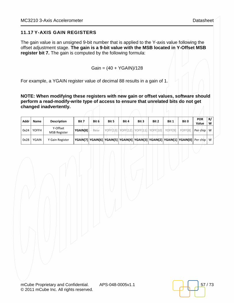
MC3210 3-Axis Accelerometer Datasheet
mCube Proprietary and Confidential. APS-048-0005v1.1 57 / 73 © 2011 mCube Inc. All rights reserved.
11.17 Y-AXIS GAIN REGISTERS
The gain value is an unsigned 9-bit number that is applied to the Y-axis value following the offset adjustment stage. The gain is a 9-bit value with the MSB located in Y-Offset MSB register bit 7. The gain is computed by the following formula:
Gain = (40 + YGAIN)/128
For example, a YGAIN register value of decimal 88 results in a gain of 1.
NOTE: When modifying these registers with new gain or offset values, software should perform a read-modify-write type of access to ensure that unrelated bits do not get changed inadvertently.
Addr Name Description Bit 7 Bit 6 Bit 5 Bit 4 Bit 3 Bit 2 Bit 1 Bit 0 POR
Value R/W
0x24 YOFFH Y-Offset
MSB Register YGAIN[8] Resv YOFF[13] YOFF[12] YOFF[11] YOFF[10] YOFF[9] YOFF[8] Per chip W
0x28 YGAIN Y Gain Register YGAIN[7] YGAIN[6] YGAIN[5] YGAIN[4] YGAIN[3] YGAIN[2] YGAIN[1] YGAIN[0] Per chip W

MC3210 3-Axis Accelerometer Datasheet
mCube Proprietary and Confidential. APS-048-0005v1.1 58 / 73 © 2011 mCube Inc. All rights reserved.
11.18 Z-AXIS GAIN REGISTERS
The gain value is an unsigned 9-bit number that is applied to the Z-axis value following the offset adjustment stage. The gain is a 9-bit value with the MSB located in Z-Offset MSB register bit 7. The gain is computed by the following formula:
Gain = (40 + ZGAIN)/128
For example, a ZGAIN register value of decimal 88 results in a gain of 1.
NOTE: When modifying these registers with new gain or offset values, software should perform a read-modify-write type of access to ensure that unrelated bits do not get changed inadvertently.
Addr Name Description Bit 7 Bit 6 Bit 5 Bit 4 Bit 3 Bit 2 Bit 1 Bit 0 POR
Value R/W
0x26 ZOFFH Z-Offset
MSB Register ZGAIN[8] Resv ZOFF[13] ZOFF[12] ZOFF[11] ZOFF[10] ZOFF[9] ZOFF[8] Per chip W
0x29 ZGAIN Z Gain Register ZGAIN[7] ZGAIN[6] ZGAIN[5] ZGAIN[4] ZGAIN[3] ZGAIN[2] ZGAIN[1] ZGAIN[0] Per chip W

MC3210 3-Axis Accelerometer Datasheet
mCube Proprietary and Confidential. APS-048-0005v1.1 59 / 73 © 2011 mCube Inc. All rights reserved.
11.19 SHAKE_TH: SHAKE THRESHOLD REGISTER
SHAKE_TH has a baseline value of 1.3g plus a threshold, SHAKE_TH. The shake threshold can range from 0.925g to 1.672g. The value is an 8-bit signed 2‟s complement number. The resolution is approximately 2.9mg/bit. See also Section 9.4 Shake Detection.
Shake Event = ( mag(X) > 1.3g + SHAKE_TH ) or
( mag(Y) > 1.3g + SHAKE_TH ) or
( mag(Z) > 1.3g + SHAKE_TH )
Addr Name Description Bit 7 Bit 6 Bit 5 Bit 4 Bit 3 Bit 2 Bit 1 Bit 0 POR
Value R/W
0x2B SHAKE_TH Shake Threshold
Register Signed 2’s complement value 0x00 W
SHAKE_TH[7:0] Description (~2.9mg/LSB)
0x80 Shake threshold is 0.925g
0x00 Shake threshold is 1.3g
0x7F Shake threshold is 1.672g
Table 34. SHAKE_TH Threshold Register Settings
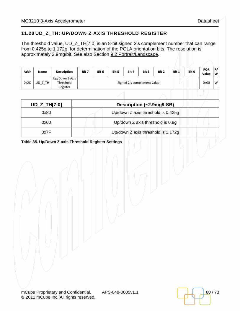
MC3210 3-Axis Accelerometer Datasheet
mCube Proprietary and Confidential. APS-048-0005v1.1 60 / 73 © 2011 mCube Inc. All rights reserved.
11.20 UD_Z_TH: UP/DOWN Z AXIS THRESHOLD REGISTER
The threshold value, UD_Z_TH[7:0] is an 8-bit signed 2‟s complement number that can range from 0.425g to 1.172g, for determination of the POLA orientation bits. The resolution is approximately 2.9mg/bit. See also Section 9.2 Portrait/Landscape.
Addr Name Description Bit 7 Bit 6 Bit 5 Bit 4 Bit 3 Bit 2 Bit 1 Bit 0 POR
Value R/W
0x2C UD_Z_TH Up/Down Z Axis
Threshold Register
Signed 2’s complement value 0x00 W
UD_Z_TH[7:0] Description (~2.9mg/LSB)
0x80 Up/down Z axis threshold is 0.425g
0x00 Up/down Z axis threshold is 0.8g
0x7F Up/down Z axis threshold is 1.172g
Table 35. Up/Down Z-axis Threshold Register Settings

MC3210 3-Axis Accelerometer Datasheet
mCube Proprietary and Confidential. APS-048-0005v1.1 61 / 73 © 2011 mCube Inc. All rights reserved.
11.21 UD_X_TH: UP/DOWN X AXIS THRESHOLD REGISTER
This 8-bit unsigned value is an offset that is added to the magnitude of the X-axis accelerometer measurement. The range of the offset is 0g to 0.747g; the resolution is approximately 2.9mg/bit. See also Section 9.2 Portrait/Landscape.
Increasing this value in conjunction with the RL_Y_TH: Right/Left Y Axis Threshold Register widens the deadband in portrait /landscape detection.
For most applications, the same value should be written to both registers.
Addr Name Description Bit 7 Bit 6 Bit 5 Bit 4 Bit 3 Bit 2 Bit 1 Bit 0 POR
Value R/W
0x2D UD_X_TH Up/Down X Axis
Threshold Register
Unsigned value 0x00 W
UD_X_TH[7:0] Description (~2.9mg/LSB)
0x00 Up/down X threshold offset is 0g
0xFF Up/down X threshold offset is +0.747g
Table 36. Up/Down X-axis Threshold Register Settings

MC3210 3-Axis Accelerometer Datasheet
mCube Proprietary and Confidential. APS-048-0005v1.1 62 / 73 © 2011 mCube Inc. All rights reserved.
11.22 RL_Z_TH: RIGHT/LEFT Z AXIS THRESHOLD REGISTER
The threshold value, RL_Z_TH[7:0] is an 8-bit signed 2‟s complement number that can range from 0.425g to 1.172g, for determination of the POLA orientation bits. The resolution is approximately 2.9mg/bit. See also Section 9.2 Portrait/Landscape.
Addr Name Description Bit 7 Bit 6 Bit 5 Bit 4 Bit 3 Bit 2 Bit 1 Bit 0 POR
Value R/W
0x2E RL_Z_TH Right/Left Z Axis
Threshold Register
Signed 2’s complement value 0x00 W
RL_Z_TH[7:0] Description (~2.9mg/LSB)
0x80 Right/left Z axis threshold is 0.425g
0x00 Right/left Z axis threshold is 0.8g
0x7F Right/left Z axis threshold is 1.172g
Table 37. Right/Left Z-axis Threshold Register Settings

MC3210 3-Axis Accelerometer Datasheet
mCube Proprietary and Confidential. APS-048-0005v1.1 63 / 73 © 2011 mCube Inc. All rights reserved.
11.23 RL_Y_TH: RIGHT/LEFT Y AXIS THRESHOLD REGISTER
This 8-bit unsigned value is an offset this is added to the magnitude of the Y-axis accelerometer measurement. The range of the offset is 0g to 0.747g; the resolution is approximately 2.9mg/bit. See also Section 9.2 Portrait/Landscape.
Increasing this value in conjunction with the UD_X_TH: Up/Down X Axis Threshold Register widens the dead-band in portrait /landscape detection.
For most applications, the same value should be written to both registers.
Addr Name Description Bit 7 Bit 6 Bit 5 Bit 4 Bit 3 Bit 2 Bit 1 Bit 0 POR
Value R/W
0x2F RL_Y_TH Right/Left Y Axis
Threshold Register
Unsigned value 0x00 W
RL_Y_TH[7:0] Description (~2.9mg/LSB)
0x00 Right/left Y-axis threshold offset is 0g
0xFF Right/left Y-axis threshold offset is +0.747g
Table 38. Right/Left Y-axis Threshold Register Settings
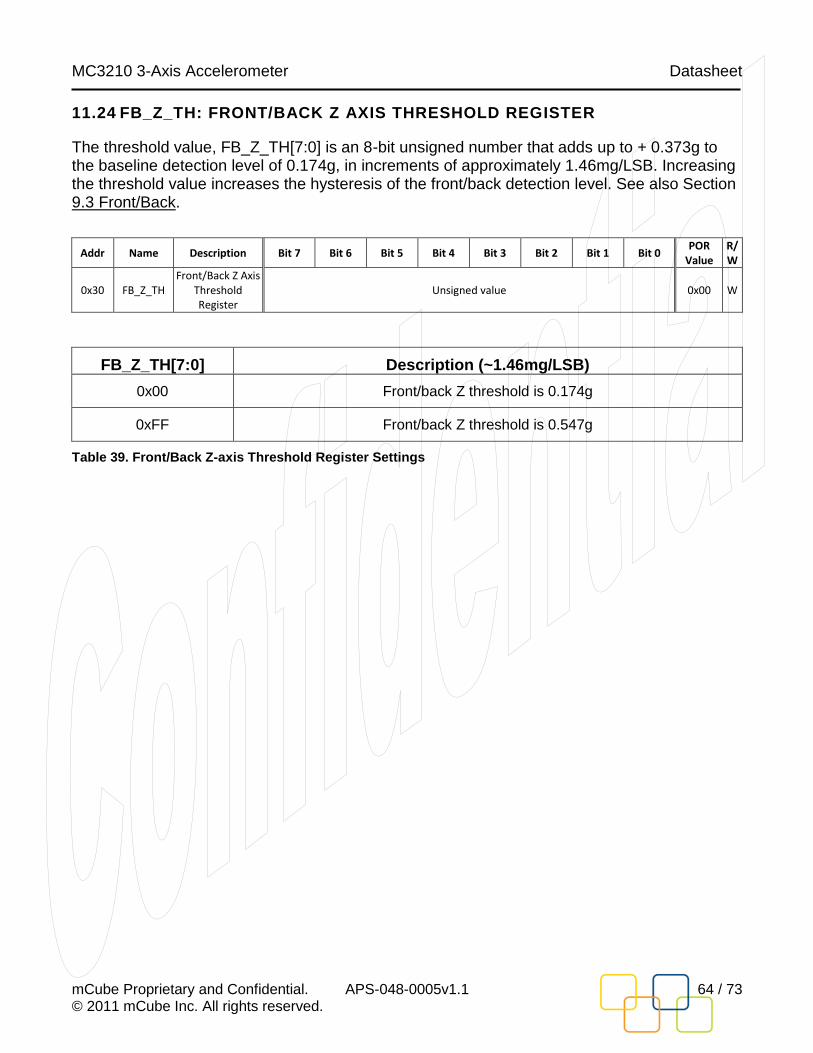
MC3210 3-Axis Accelerometer Datasheet
mCube Proprietary and Confidential. APS-048-0005v1.1 64 / 73 © 2011 mCube Inc. All rights reserved.
11.24 FB_Z_TH: FRONT/BACK Z AXIS THRESHOLD REGISTER
The threshold value, FB_Z_TH[7:0] is an 8-bit unsigned number that adds up to + 0.373g to the baseline detection level of 0.174g, in increments of approximately 1.46mg/LSB. Increasing the threshold value increases the hysteresis of the front/back detection level. See also Section 9.3 Front/Back.
Addr Name Description Bit 7 Bit 6 Bit 5 Bit 4 Bit 3 Bit 2 Bit 1 Bit 0 POR
Value R/W
0x30 FB_Z_TH Front/Back Z Axis
Threshold Register
Unsigned value 0x00 W
FB_Z_TH[7:0] Description (~1.46mg/LSB)
0x00 Front/back Z threshold is 0.174g
0xFF Front/back Z threshold is 0.547g
Table 39. Front/Back Z-axis Threshold Register Settings

MC3210 3-Axis Accelerometer Datasheet
mCube Proprietary and Confidential. APS-048-0005v1.1 65 / 73 © 2011 mCube Inc. All rights reserved.
11.25 DROP_TH: DROP THRESHOLD REGISTER
The threshold value, DROP_TH[7:0] is an 8-bit signed 2‟s complement number that adjusts the drop-detection baseline detection level of 0.5g. See also Section 9.5 Drop Detection.
Addr Name Description Bit 7 Bit 6 Bit 5 Bit 4 Bit 3 Bit 2 Bit 1 Bit 0 POR
Value R/W
0x31 DROP_TH Drop Threshold
Register Signed 2’s complement value 0x00 W
DROP_TH[7:0] Description (~2.9mg/LSB)
0x80 Drop threshold is 0.125g
0x00 Drop threshold is 0.5g
0x7F Drop threshold is 0.872g
Table 40. Drop Threshold Register Settings
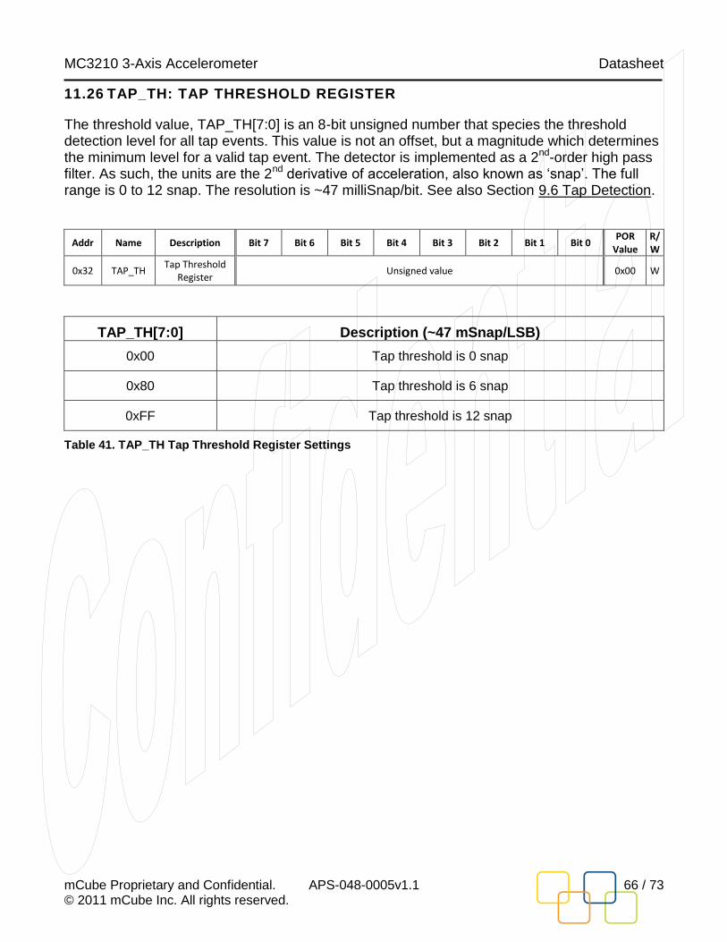
MC3210 3-Axis Accelerometer Datasheet
mCube Proprietary and Confidential. APS-048-0005v1.1 66 / 73 © 2011 mCube Inc. All rights reserved.
11.26 TAP_TH: TAP THRESHOLD REGISTER
The threshold value, TAP_TH[7:0] is an 8-bit unsigned number that species the threshold detection level for all tap events. This value is not an offset, but a magnitude which determines the minimum level for a valid tap event. The detector is implemented as a 2nd-order high pass filter. As such, the units are the 2nd derivative of acceleration, also known as „snap‟. The full range is 0 to 12 snap. The resolution is ~47 milliSnap/bit. See also Section 9.6 Tap Detection.
Addr Name Description Bit 7 Bit 6 Bit 5 Bit 4 Bit 3 Bit 2 Bit 1 Bit 0 POR
Value R/W
0x32 TAP_TH Tap Threshold
Register Unsigned value 0x00 W
TAP_TH[7:0] Description (~47 mSnap/LSB)
0x00 Tap threshold is 0 snap
0x80 Tap threshold is 6 snap
0xFF Tap threshold is 12 snap
Table 41. TAP_TH Tap Threshold Register Settings

MC3210 3-Axis Accelerometer Datasheet
mCube Proprietary and Confidential. APS-048-0005v1.1 67 / 73 © 2011 mCube Inc. All rights reserved.
11.27 PCODE: PRODUCT CODE
This register returns a value specific to the part number of this mCube device, noted below.
Addr Name Description Bit 7 Bit 6 Bit 5 Bit 4 Bit 3 Bit 2 Bit 1 Bit 0 POR
Value R/W
0x3B PCODE Product Code
Register 0x90 0x90 R
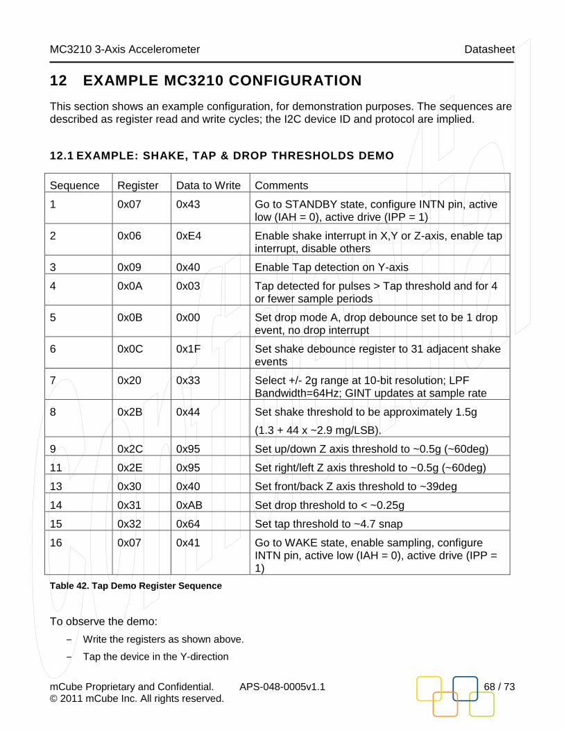
MC3210 3-Axis Accelerometer Datasheet
mCube Proprietary and Confidential. APS-048-0005v1.1 68 / 73 © 2011 mCube Inc. All rights reserved.
12 EXAMPLE MC3210 CONFIGURATION
This section shows an example configuration, for demonstration purposes. The sequences are described as register read and write cycles; the I2C device ID and protocol are implied.
12.1 EXAMPLE: SHAKE, TAP & DROP THRESHOLDS DEMO
Sequence Register Data to Write Comments
1 0x07 0x43 Go to STANDBY state, configure INTN pin, active low (IAH = 0), active drive (IPP = 1)
2 0x06 0xE4 Enable shake interrupt in X,Y or Z-axis, enable tap interrupt, disable others
3 0x09 0x40 Enable Tap detection on Y-axis
4 0x0A 0x03 Tap detected for pulses > Tap threshold and for 4 or fewer sample periods
5 0x0B 0x00 Set drop mode A, drop debounce set to be 1 drop event, no drop interrupt
6 0x0C 0x1F Set shake debounce register to 31 adjacent shake events
7 0x20 0x33 Select +/- 2g range at 10-bit resolution; LPF Bandwidth=64Hz; GINT updates at sample rate
8 0x2B 0x44 Set shake threshold to be approximately 1.5g
(1.3 + 44 x ~2.9 mg/LSB).
9 0x2C 0x95 Set up/down Z axis threshold to ~0.5g (~60deg)
11 0x2E 0x95 Set right/left Z axis threshold to ~0.5g (~60deg)
13 0x30 0x40 Set front/back Z axis threshold to ~39deg
14 0x31 0xAB Set drop threshold to < ~0.25g
15 0x32 0x64 Set tap threshold to ~4.7 snap
16 0x07 0x41 Go to WAKE state, enable sampling, configure INTN pin, active low (IAH = 0), active drive (IPP = 1)
Table 42. Tap Demo Register Sequence
To observe the demo:
‒ Write the registers as shown above.
‒ Tap the device in the Y-direction

MC3210 3-Axis Accelerometer Datasheet
mCube Proprietary and Confidential. APS-048-0005v1.1 69 / 73 © 2011 mCube Inc. All rights reserved.
‒ Observe interrupt trigger and TAPD tap detection bit
‒ Read TILT: Status Register to reset the Tap interrupt
‒ Tap the device in the X and Z directions
‒ Observer no interrupt triggers
‒ Rotate the device around in 3D-space
‒ Observe that the up/down/left/right indications trip at a very steep angle (the chip must be tilted a lot in order for UNKNOWN to not be indicated by the hardware)
‒ Observe that there is very little hysteresis between the FRONT and BACK readings

MC3210 3-Axis Accelerometer Datasheet
mCube Proprietary and Confidential. APS-048-0005v1.1 70 / 73 © 2011 mCube Inc. All rights reserved.
13 INDEX OF TABLES
Table 1. Order Information.........................................................................................................................................5
Table 2. Pin Description ..............................................................................................................................................8
Table 3. Absolute Maximum Ratings ....................................................................................................................... 10
Table 4. Sensor Characteristics ................................................................................................................................ 11
Table 5. Electrical Characteristics ............................................................................................................................ 12
Table 6. I2C Electrical and Timing Characteristics ................................................................................................... 13
Table 7. I2C Timing Characteristics .......................................................................................................................... 14
Table 8. Summary of Resolution, Range, and Scaling ............................................................................................. 15
Table 9. Operational States ..................................................................................................................................... 17
Table 10. Forcing Operational States ...................................................................................................................... 18
Table 11. Interrupt Support ..................................................................................................................................... 20
Table 12. Detection Logic Event Evaluation ............................................................................................................ 22
Table 13. Portrait/Landscape Event Evaluation Criteria ......................................................................................... 25
Table 14. Some Approximate X and Y-axis Portrait/Landscape Evaluation Angles and Values .............................. 26
Table 15. Some Approximate Z-axis Portrait/Landscape Evaluation Angles and Values ........................................ 26
Table 16. Portrait/Landscape TILT: Status Register Assignments ........................................................................... 27
Table 17. BAFR Bit Assignments in the TILT: Status Register .................................................................................. 29
Table 18. Front/Back Event Evaluation ................................................................................................................... 29
Table 19. Approximate Front/Back Evaluation Angles and Values ......................................................................... 29
Table 20. SHAKE Event Evaluation (Baseline + Offset) ............................................................................................ 30
Table 21. Drop Event Evaluation ............................................................................................................................. 32
Table 22. Default Tap Event Evaluation................................................................................................................... 34
Table 23. Register Summary .................................................................................................................................... 40
Table 24. TILT Status Register Settings .................................................................................................................... 41
Table 25. Operational State Status Register ............................................................................................................ 43
Table 26. Interrupt Enable Register Settings ........................................................................................................... 44
Table 27. Mode Register Functionality .................................................................................................................... 45
Table 28. TAPEN Register Settings........................................................................................................................... 46
Table 29. TAPP Tap Pulse Register Settings ............................................................................................................. 47
Table 30. Drop Event Control Register Settings ...................................................................................................... 48
Table 31. SH_DB Shake Debounce Register Settings .............................................................................................. 49

MC3210 3-Axis Accelerometer Datasheet
mCube Proprietary and Confidential. APS-048-0005v1.1 71 / 73 © 2011 mCube Inc. All rights reserved.
Table 32. Extended Accelerometer Registers.......................................................................................................... 50
Table 33. OUTCFG Resolution and Range Select Register Settings ......................................................................... 52
Table 34. SHAKE_TH Threshold Register Settings ................................................................................................... 59
Table 35. Up/Down Z-axis Threshold Register Settings .......................................................................................... 60
Table 36. Up/Down X-axis Threshold Register Settings .......................................................................................... 61
Table 37. Right/Left Z-axis Threshold Register Settings .......................................................................................... 62
Table 38. Right/Left Y-axis Threshold Register Settings .......................................................................................... 63
Table 39. Front/Back Z-axis Threshold Register Settings ........................................................................................ 64
Table 40. Drop Threshold Register Settings ............................................................................................................ 65
Table 41. TAP_TH Tap Threshold Register Settings ................................................................................................. 66
Table 42. Tap Demo Register Sequence .................................................................................................................. 68
MC3210 3-Axis Accelerometer Datasheet
mCube Proprietary and Confidential. APS-048-0005v1.1 72 / 73 © 2011 mCube Inc. All rights reserved.
14 REVISION HISTORY
Date Revision Description
2011-10 APS-048-0005v1.0 Separated combined datasheet into individual documents.
Changed temp drift typical spec.
Clarified voltage limits as hard limits.
Changed sensitivity specs for symmetry around typical value.
Noted capacitance and sample rate tolerance are not tested in production.
Fixed typo in example sequence 12.1.
Updated PCODE values.
Some minor text formatting of footnotes.
Added Offset and Gain registers.
Adjusted threshold values for more detail.
Altered POLA pictures.
Corrected Front/Back event detection criteria.
Corrected UD_Z_TH and RL_Z_TH values.
2011-10 APS-048-0005v1.1 Changed chip reference in I2C pictures.
Clarified sensitivity not tested in production.
MC3210 3-Axis Accelerometer Datasheet
mCube Proprietary and Confidential. APS-048-0005v1.1 73 / 73 © 2011 mCube Inc. All rights reserved.
15 LEGAL
1. M-CUBE reserves the right to make corrections, modifications, enhancements, improvements and other changes to its
products and to this document at any time and discontinue any product without notice. The information contained in this
document has been carefully checked and is believed to be accurate. However, M-CUBE shall assume no responsibilities for
inaccuracies and make no commitment to update or to keep current the information contained in this document.
2. M-CUBE products are designed only for commercial and normal industrial applications and are not suitable for other
purposes, such as: medical life support equipment; nuclear facilities; critical care equipment; military / aerospace;
automotive; security or any other applications, the failure of which could lead to death, personal injury or environmental or
property damage. Use of the products in unsuitable applications are at the customer’s own risk and expense.
3. M-CUBE shall assume no liability for incidental, consequential or special damages or injury that may result from
misapplication or improper use of operation of the product.
4. No license, express or implied, by estoppel or otherwise, to any intellectual property rights of M-CUBE or any third
party is granted under this document.
5. M-CUBE makes no warranty or representation of non-infringement of intellectual property rights of any third party with
respect to the products. M-CUBE specifically excludes any liability to the customers or any third party regarding
infringement of any intellectual property rights, including the patent, copyright, trademark or trade secret rights of any third
party, relating to any combination, machine, or process in which the M-CUBE products are used.
6. Examples of use described herein are provided solely to guide use of M-CUBE products and merely indicate targeted
characteristics, performance and applications of products. M-CUBE shall assume no responsibility for any intellectual
property claims or other problems that may result from applications based on the examples described herein
7. Information described in this document including parameters, application circuits and its constants and calculation
formulas, programs and control procedures are provided for the purpose of explaining typical operation and usage. “Typical”
parameters that may be provided in M-CUBE data sheets and/or specifications can and do vary in different applications and
actual performance may vary over time. All operating parameters including “Typicals,” must be validated for each customer
application by customer’s technical experts. In no event shall the information described be regarded as a guarantee of
conditions or characteristics of the products. Therefore, the customer should evaluate the design sufficiently as whole system
under the consideration of various external or environmental conditions and determine their application at the customer’s
own risk. M-CUBE shall assume no responsibility or liability for claims, damages, costs and expenses caused by the
customer or any third party, owing to the use of the above information.
is a trademark of M-CUBE, Inc.
M-CUBE and the M-CUBE logo are trademarks of M-CUBE, Inc.,
All other product or service names are the property of their respective owners.
© M-CUBE, Inc. 2011. All rights reserved.