May 2017, Volume 4, Issue 05 JETIR (ISSN 2349 5162) POWER ...
10
May 2017, Volume 4, Issue 05 JETIR (ISSN-2349-5162) JETIR1705035 Journal of Emerging Technologies and Innovative Research (JETIR) www.jetir.org 151 POWER QUALITY ENHANCEMENT USING DUAL VOLTAGE SOURCE INVERTER 1 Maria Pius Pallan, 2 Jisi N k 1 P.G. Scholar, 2 Assistant Professor 1 Department of Electrical & Electronics Engineering 1 Thejus Engineering College, Thrissur, Kerala Abstract— Maintaining power quality is an important part which has to be considered while the microgrid system is connected to the main grid. The introduction of power electronics devices and electrical loads with unbalanced nonlinear currents has degraded the power quality in the power distribution network. This paper presents a dual voltage source inverter (DVSI) scheme to improve the power quality and reliability of the microgrid system. The proposed system is comprised of two inverters, main voltage source inverter (MVSI) and auxiliary voltage source inverter (AVSI) which enables it to inject real power, and reactive, harmonic, unbalanced load compensations respectively. The control algorithms are developed using instantaneous symmetrical component theory (ISCT) to operate DVSI in grid sharing and grid injecting modes. The method has the advantages of increased reliability, reduction in filter size, improved flexibility, and better utilization of microgrid power. The performance of the system is validated through MATLAB simulations. Index Terms— Grid-connected inverter, instantaneous symmetrical component theory (ISCT), microgrid, power quality. I. INTRODUCTION Distributed generation (DG) systems are presented as a appropriate choice to offer high reliable electrical power supply. The concept is quite attractive when different kinds of energy resources are available, such as photovoltaic panels, fuel cells, or speed wind turbines etc [1]. Most of these resources require power electronic interfaces to make up local ac grids. Generally inverters or ac-to-ac converters are linked to an ac common bus to share properly the disperse loads connected to the local grid. The majority of distributed generation (DG) units are connected to grid/load using power electronics converters. Current-controlled voltage-sourced inverters (VSIs) are generally used for grid connection. Under the smart grid environment, DG units should be incorporated in the system operational control framework, where it can be used to improve system reliability by providing backup generation in isolated mode, and to provide ancillary services in the grid-connected mode. These DG units with coordinated control of local generation and storage facilities form a microgrid [2]. Among various renewable energy resources, solar photovoltaic (PV) and wind are fast growing technologies. However, their intermittent nature has introduced many technical issues, including power quality, load management, stability and controls, reliability, and voltage regulation. With the progress in power electronics and digital signal processors, the power electronic interfaces are effectively used to determine some of the issues pointed above at the point of common coupling (PCC) [3]. Therefore, the DG systems are required to comply with strict technical and regulatory frameworks to ensure safe, reliable and efficient operation of overall network. With the improvement in power electronics and digital control technology, the DG systems can now be actively controlled to enhance the system operation with improved PQ at PCC. However, the extensive use of power electronics based equipment and non-linear loads at PCC generate harmonic currents, which may deteriorate the quality of power [4]. For technological progress and environmental stability use of renewable energy sources along with main grid is important. The coordinated operation of grid and distributed energy units along with storage facilities form a microgrid. This structure and operation of the microgrid is explained in [5]. In [6] it describes the operation of grid connected inverters and how it plays important role in exchanging power from DG to grid and connected loads. It also explains how a grid connected DGs work in grid sharing mode and grid injecting mode. A grid connected four phase four leg shunt and series compensators are used to maintain power quality of the system using proportional filter resonant control loop is given in [7]. This control maintains both quality of power as well as quality of current flowing between microgrid and utility grid. But it fails to limit large fault current during short circuit faults. Paper [8] is a simple system consisting of PV array, voltage source inverter, grid filter and an electric grid where nonlinear controller based on Lyapunov approach is used to control VSI. It improves stability of the system and also power factor unity in the side of the grid. The main drawback of this paper is that it is difficult to implement and is very sensitive to frequency variations. An inductive active filtering method is used in [9] to improve power quality. In this harmonic components can be effectively prevented from flowing in to the primary winding of the transformer. Theory of instantaneous symmetrical components has been applied to formulate various load compensation strategies under different supply voltages is given in [10]. Here symmetrical components of voltage and current are measured to generate PWM signals. But the THD cannot be minimized below 5% using this. Paper [11] describes a filter designed to incorporate an isolating transformer and a design of complementary control that rejects grid disturbances. It maintains good waveform quality and achieves real and reactive power control. The system has the disadvantage of sensitivity to large disturbances and faults. In recent times, a few control strategies for grid connected inverters incorporating PQ problems and its solution have been proposed. An inverter operates as active inductor at a certain frequency to absorb the harmonic current [12]. But the exact calculation of network inductance in real-time is difficult and it may deteriorate the control performance. A similar approach with a shunt active filter which acts as active conductance to damp out the harmonics in distribution network is proposed in [13]. In [14], a control strategy based on p-q theory for renewable interfacing inverter is presented. In this paper both load and inverter current sensing is required to compensate the load current harmonics. This paper explains a dual voltage source inverter, where the power generated from the microgrid is injected as real power by MVSI and unbalanced load compensations is performed by AVSI. Three phase three leg inverter topology is used for both AVSI and MVSI. They are connected to the grid at the point of common coupling (PCC) using coupling inductance. The block diagram of the system is shown in Fig.1. If adequate renewable power is offered at the dc-link then the rated capacity of MVSI always injects real power to the grid. In DVSI, power
Transcript of May 2017, Volume 4, Issue 05 JETIR (ISSN 2349 5162) POWER ...

May 2017, Volume 4, Issue 05 JETIR (ISSN-2349-5162)
JETIR1705035 Journal of Emerging Technologies and Innovative Research (JETIR) www.jetir.org 151
POWER QUALITY ENHANCEMENT USING DUAL
VOLTAGE SOURCE INVERTER 1Maria Pius Pallan,
2Jisi N k
1 P.G. Scholar,
2Assistant Professor
1 Department of Electrical & Electronics Engineering
1 Thejus Engineering College, Thrissur, Kerala
Abstract— Maintaining power quality is an important part which has to be considered while the microgrid system is connected to the
main grid. The introduction of power electronics devices and electrical loads with unbalanced nonlinear currents has degraded the power
quality in the power distribution network. This paper presents a dual voltage source inverter (DVSI) scheme to improve the power quality
and reliability of the microgrid system. The proposed system is comprised of two inverters, main voltage source inverter (MVSI) and
auxiliary voltage source inverter (AVSI) which enables it to inject real power, and reactive, harmonic, unbalanced load compensations
respectively. The control algorithms are developed using instantaneous symmetrical component theory (ISCT) to operate DVSI in grid
sharing and grid injecting modes. The method has the advantages of increased reliability, reduction in filter size, improved flexibility, and
better utilization of microgrid power. The performance of the system is validated through MATLAB simulations.
Index Terms— Grid-connected inverter, instantaneous symmetrical component theory (ISCT), microgrid, power quality.
I. INTRODUCTION
Distributed generation (DG) systems are presented as a appropriate choice to offer high reliable electrical power supply. The concept is
quite attractive when different kinds of energy resources are available, such as photovoltaic panels, fuel cells, or speed wind turbines etc [1].
Most of these resources require power electronic interfaces to make up local ac grids. Generally inverters or ac-to-ac converters are linked to
an ac common bus to share properly the disperse loads connected to the local grid.
The majority of distributed generation (DG) units are connected to grid/load using power electronics converters. Current-controlled
voltage-sourced inverters (VSIs) are generally used for grid connection. Under the smart grid environment, DG units should be incorporated
in the system operational control framework, where it can be used to improve system reliability by providing backup generation in isolated
mode, and to provide ancillary services in the grid-connected mode. These DG units with coordinated control of local generation and storage
facilities form a microgrid [2].
Among various renewable energy resources, solar photovoltaic (PV) and wind are fast growing technologies. However, their intermittent
nature has introduced many technical issues, including power quality, load management, stability and controls, reliability, and voltage
regulation. With the progress in power electronics and digital signal processors, the power electronic interfaces are effectively used to
determine some of the issues pointed above at the point of common coupling (PCC) [3]. Therefore, the DG systems are required to comply
with strict technical and regulatory frameworks to ensure safe, reliable and efficient operation of overall network. With the improvement in
power electronics and digital control technology, the DG systems can now be actively controlled to enhance the system operation with
improved PQ at PCC. However, the extensive use of power electronics based equipment and non-linear loads at PCC generate harmonic
currents, which may deteriorate the quality of power [4].
For technological progress and environmental stability use of renewable energy sources along with main grid is important. The
coordinated operation of grid and distributed energy units along with storage facilities form a microgrid. This structure and operation of the
microgrid is explained in [5]. In [6] it describes the operation of grid connected inverters and how it plays important role in exchanging
power from DG to grid and connected loads. It also explains how a grid connected DGs work in grid sharing mode and grid injecting mode.
A grid connected four phase four leg shunt and series compensators are used to maintain power quality of the system using proportional filter
resonant control loop is given in [7]. This control maintains both quality of power as well as quality of current flowing between microgrid
and utility grid. But it fails to limit large fault current during short circuit faults. Paper [8] is a simple system consisting of PV array, voltage
source inverter, grid filter and an electric grid where nonlinear controller based on Lyapunov approach is used to control VSI. It improves
stability of the system and also power factor unity in the side of the grid. The main drawback of this paper is that it is difficult to implement
and is very sensitive to frequency variations. An inductive active filtering method is used in [9] to improve power quality. In this harmonic
components can be effectively prevented from flowing in to the primary winding of the transformer. Theory of instantaneous symmetrical
components has been applied to formulate various load compensation strategies under different supply voltages is given in [10]. Here
symmetrical components of voltage and current are measured to generate PWM signals. But the THD cannot be minimized below 5% using
this. Paper [11] describes a filter designed to incorporate an isolating transformer and a design of complementary control that rejects grid
disturbances. It maintains good waveform quality and achieves real and reactive power control. The system has the disadvantage of
sensitivity to large disturbances and faults.
In recent times, a few control strategies for grid connected inverters incorporating PQ problems and its solution have been proposed. An
inverter operates as active inductor at a certain frequency to absorb the harmonic current [12]. But the exact calculation of network
inductance in real-time is difficult and it may deteriorate the control performance. A similar approach with a shunt active filter which acts as
active conductance to damp out the harmonics in distribution network is proposed in [13]. In [14], a control strategy based on p-q theory for
renewable interfacing inverter is presented. In this paper both load and inverter current sensing is required to compensate the load current
harmonics.
This paper explains a dual voltage source inverter, where the power generated from the microgrid is injected as real power by MVSI and
unbalanced load compensations is performed by AVSI. Three phase three leg inverter topology is used for both AVSI and MVSI. They are
connected to the grid at the point of common coupling (PCC) using coupling inductance. The block diagram of the system is shown in Fig.1.
If adequate renewable power is offered at the dc-link then the rated capacity of MVSI always injects real power to the grid. In DVSI, power

May 2017, Volume 4, Issue 05 JETIR (ISSN-2349-5162)
JETIR1705035 Journal of Emerging Technologies and Innovative Research (JETIR) www.jetir.org 152
loss across the switches of each inverter is reduced. As the main inverter is supplying real power, the inverter has to track the fundamental
positive sequence components of current that results in reduction of main inverter bandwidth. Smaller size modular inverters work at high
switching frequencies with a small size interfacing inductor, so the cost of filter gets reduced. The control algorithm to operate DVSI is
developed by using ISCT theory [15].
Fig.1 Block diagram of the system
The paper is arranged as follows: Section II describes the system under consideration. Design parameter for the proposed system is
given in Section III. The proposed control for grid interfacing inverter is explained in Section IV. A digital simulation study is presented in
Section V and, finally, Section VI concludes the paper
II. DUAL VOLTAGE SOURCE INVERTER
General topology of the system is shown in Fig.2. A model of the grid connected DG system is developed to find out the impact of
nonlinear and unbalanced loads on the grid current of the DG. The DVSI scheme consists of 2 inverters which are linked to the grid at point
of common coupling (PCC) and supplying unbalanced loads. A neutral point clamped (NPC) inverter is used as an auxiliary voltage source
inverter that compensates reactive, harmonic and unbalanced components in load currents. Capacitors C1 and C2 represents the split
capacitor topology of dc-link of the AVSI. A three leg inverter is used as the main voltage source inverter that supply the power generated
from the distributed energy resources (DER) to grid. The DER can be either dc source or ac source. Here resistance ( fR ) and inductance
( fL ) represents the feeder impedance. Also )(abcgi represents grid currents, )(abcgmi represents MVSI currents. )(abcgxi represent AVSI
currents, )(abcli represents load currents, )(abctv represents PCC voltages.
Fig.2 Topology of the system
In this model, DVSI is used to produce the compensating current and is injected into the utility power source grid. This cancels the
harmonic components drawn by the non-linear and unbalanced loads and keeps the utility line current sinusoidal. An inductor filter is used to
reduce the high-frequency switching components generated due to the switching of power electronic switches in the inverters. Due to the
Coupling inductance
Main grid Transmission system Load
DC BESS 3 Phase 3 leg MVSI
DC link with Neutral point
clamped
Coupling inductance
Load
Control
Control
3 phase 3 leg AVSI
PCC

May 2017, Volume 4, Issue 05 JETIR (ISSN-2349-5162)
JETIR1705035 Journal of Emerging Technologies and Innovative Research (JETIR) www.jetir.org 153
presence of the feeder impedance, PCC voltage is affected with harmonics. The dq0 transformation is used to take out the fundamental
positive sequence components of this PCC voltage. Instantaneous symmetrical component theory based algorithm is proposed for reference
signal generation. The reference current calculator will extract the reactive and harmonic current component of the load current and produce
the compensating current. The hysteresis band current controller generates gating pulse in a proper series for the conduction of IGBT by
comparing the reference current with actual current.
Providing multifunctionalities in a single inverter degrades either the real power injection or the load compensation capabilities of the
system. The various advantages of the proposed DVSI scheme over this are increased reliability, lower bandwidth requirement of the main
inverter, lower cost due to reduction in filter size, and better utilization of microgrid power while using reduced dc-link voltage rating for the
main inverter.
In this scheme, the total load current is shared between AVSI and MVSI and hence reduces the failure rate of inverter switches.
Moreover, if one inverter fails, the other can carry on its operation. This reduces the lost energy and hence the down time cost. Thus
improves its reliability. Also the current supplied by each inverter is reduced and hence the current rating of individual filter inductor
reduces. This reduction in current rating reduces the filter size. As both the inverters are fed from separate dc links which let them to operate
independently, thus increasing the flexibility of the system. DVSI scheme helps to make use of full capacity of MVSI to transfer the whole
power generated by DG units as real power to ac bus, as there is AVSI for harmonic and reactive power compensation. This increases the
active power injection capacity of DGs in microgrid.
III. DESIGN PARAMETERS FOR DVSI SCHEME
A. AVSI
The major parameters of AVSI are dc-link voltage ( dcV ), dc storage capacitors (C1 and C2), interfacing inductance( fxL ), and hysteresis
band (± xh ). They are chosen based on the design technique of split capacitor DSTATCOM topology [16]. The dc-link voltage across the
capacitor is taken as 1.6 times the peak of phase voltage. The total dc-link voltage reference ( dcrefV ) is taken to be 1040 V. The change in
dc-link voltage during transients is responsible for choosing the values of dc capacitors of AVSI. Let total load rating is S kVA. In the worst
case, the load power may differ from minimum to maximum, i.e., from 0 to S kVA. To retain the load power demand during transient, AVSI
needs to exchange real power. During the transient this transfer of real power will result in variation of capacitor voltage from its reference
value. Assume that the voltage controller takes n cycles, i.e., nT seconds to act, where T is the system time period. Hence, maximum energy
exchange by AVSI during transient will be nST. This energy will be equivalent to change in the capacitor stored energy. Therefore
nSTVVC dcdcr 122
12
1 (1)
where dcrV and 1dcV are the reference dc voltage and maximum permissible dc voltage across C1 during transient, respectively. Here, S =5
kVA, dcrV = 520 V, 1dcV = 0.8 * dcrV or 1.2* dcrV , n=1, and T= 0.02s. Substituting these values in (1), the dclink capacitance (C1) is
calculated to be 2000 μF. Same value of capacitance is selected for C2. The interfacing inductance is given by
max4
6.1
fh
VL
x
mfx
(2)
Assuming a maximum switching frequency ( maxf ) of 10 kHz and hysteresis band ( xh ) as 5% of load current (0.5 A), the value of fxL is
calculated to be 26 mH.
B. MVSI
A three leg inverter is used as a MVSI. Power generated from DER such as PV or wind energy system is coupled to dc link of the inverter.
The dc-link voltage is taken as 1.15* mlV where mlV is the peak value of line voltage. At unity factor MVSI supply a balanced sinusoidal
current, so zero switching harmonics are missing in the output current of MVSI. Thus filter requirement for MVSI is reduced.
IV. PROPOSED CONTROL SCHEME
The generation of reference current for AVSI and MVSI is the major process involved in the control technique. The scheme has three
main parts, fundamental voltage extraction, the current reference generation scheme, and the proposed current controller. The control
algorithm is based on instantaneous symmetrical component theory (ISCT). The proposed system is developed in dq frame. PLL is used to
decide the frequency and phase angle reference of the PCC (point of common coupling). Because of the occurrence of feeder impedance, PCC
voltages are distorted. Therefore, the fundamental positive sequence components of the PCC voltages are extracted for the reference current
generation. The reference current is then given to this hysteresis band current controller and it generates switching signals for the desired
sinusoidal reference current. The scheme can thus simultaneously address and eliminate effects of the nonlinear local loads and distorted grid
voltage conditions on the grid current quality.
A. Instantaneous Symmetrical Component Theory
The control scheme is based on (d-q) theory. In calculation part only algebraic calculations are involve which makes this control scheme
easy as compare to other algorithms .SRF (synchronous reference frame) works on park’s transformation (d-q) and inverse parks
transformation. The transformation is done from three phase abc to d-q to convert the distorted PCC voltages to balanced sinusoidal voltages.
It is represented as the equations shown below.
where
tc
tb
ta
to
tq
td
v
v
v
c
v
v
v
2
1
2
1
2
13
2cos
3
2coscos
3
2sin
3
2sinsin
3
2
c
May 2017, Volume 4, Issue 05 JETIR (ISSN-2349-5162)
JETIR1705035 Journal of Emerging Technologies and Innovative Research (JETIR) www.jetir.org 154
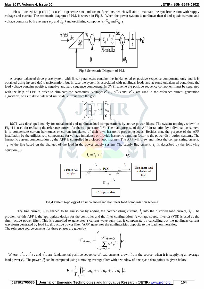
Phase Locked Loop (PLL) is used to generate sine and cosine functions, which will aid to maintain the synchronization with supply
voltage and current. The schematic diagram of PLL is shown in Fig.3. When the power system is nonlinear then d and q axis currents and
voltage comprise both average (tdv and tqv ) and oscillating components ( tdv~ and tqv~ ).
Fig.3 Schematic Diagram of PLL
A proper balanced three phase system with linear parameters contains the fundamental or positive sequence components only and it is
obtained using inverse dq0 transformation, but in case the system is associated with nonlinear loads and at some unbalanced conditions the
load voltage contains positive, negative and zero sequence component. In DVSI scheme the positive sequence component must be separated
with the help of LPF in order to eliminate the harmonics. Voltages 1tav, 1tbv
and 1tcvare used in the reference current generation
algorithms, so as to draw balanced sinusoidal current from the grid.
ISCT was developed mainly for unbalanced and nonlinear load compensations by active power filters. The system topology shown in
Fig. 4 is used for realizing the reference current for the compensator [15]. The main purpose of the APF installation by individual consumers
is to compensate current harmonics or current imbalance of their own harmonic-producing loads. Besides that, the purpose of the APF
installation by the utilities is to compensate for voltage imbalance or provide harmonic damping factor to the power distribution systems. The
harmonic current compensation by the APF is controlled in a closed loop manner. The APF will draw and inject the compensating current,
fi to the line based on the changes of the load in the power supply system. The supply line current, si is described by the following
equation (3)
lfs iii
(3)
Fig.4 system topology of an unbalanced and nonlinear load compensation scheme
The line current, si is shaped to be sinusoidal by adding the compensating current, fi into the distorted load current, li . The
problem of this APF is the appropriate design for the controller and the filter configuration. A voltage source inverter (VSI) is used as the
shunt active power filter. This is controlled to generates a current wave such that it compensate by cancelling out the nonlinear current
waveform generated by load i.e. this active power filter (APF) generates the nonlinearities opposite to the load nonlinearities.
The reference source currents for three phases are given by
l
cbaj
tj
abctabcs p
v
vi
,,
2
1*
Where
sai*, sbi*
, and sci*are fundamental positive sequence of load currents drawn from the source, when it is supplying an average
load power lP . The power lP can be computed using a moving average filter with a window of one-cycle data points as given below
dtivivivT
P
t
Tt
lctclbtblatal
1
1
111
1
01
1
1
tq
td
T
tc
tb
ta
v
v
C
v
v
v

May 2017, Volume 4, Issue 05 JETIR (ISSN-2349-5162)
JETIR1705035 Journal of Emerging Technologies and Innovative Research (JETIR) www.jetir.org 155
where t1 is any arbitrary time instant. Finally, the reference currents for the compensator can be generated as follows:
)(*
)()(*
abcsabclabcf iii (4)
Equation (4) can be used to generate the reference filter currents using ISCT, when the entire load active power, lP is supplied by the
source and load compensation is performed by a single inverter. A change in the control algorithm is required, when it is used in DVSI
scheme. The following part discusses the formulation of control algorithm for DVSI scheme. The source currents, )(abcsi and filter currents
)(abcfi will be equivalently represented as grid currents )(abcgi and AVSI current )(abcgxi , respectively, in further sections.
B. Reference Current Generation For AVSI and MVSI
The control technique of DVSI explains the grid sharing and grid injecting mode and also compensation method by AVSI. Control
strategy is developed in such a manner that grid and MVSI together share the active load power, and AVSI supplies rest of the power
components demanded by the load. The entire control strategy is schematically represented in Fig.4
For the reference current generation of AVSI the dc-link voltage of the AVSI should be maintained constant for proper operation. This
voltage variation occurs in auxiliary inverter due to its switching and ohmic losses. These are termed as lossP and should be supplied by the
grid. An expression for lossP is derived on the condition that to maintain a constant capacitor voltage average dc capacitor current should be
zero. The deviation of this average capacitor current from zero will results in a change in capacitor voltage from a steady state value. A PI
controller is used to generate lossP term as given by
Where dcdcrefvdc vVe , dcv represents the actual voltage sensed and updated once in a cycle. In the above equation, pvK and IvK
represent the proportional and integral gains of dc-link PI controller. The lossP term thus obtained should be supplied by the grid, and
therefore AVSI reference currents for three phases (a,b and c) can be obtained as given in below. Here, the dc-link voltage PI controller gains
are selected so as to make sure stability and better dynamic response during load change.
The MVSI supplies balanced sinusoidal currents based on the available renewable power at DER. If MVSI losses are neglected, the power
injected to grid will be equal to that available at DER ( gP ). ISCT can be used to generate MVSI reference currents for three phases (a, b, and
c) and it is represented as
Where gP is the existing power at the dc link of MVSI. The reference current obtained here are tracked using HBCC. The whole
control strategy is schematically represented in Fig.5. By applying Kirchoff’s current law (KCL) at the PCC.
gmjgjljgxj iiii , for j=a,b,c
By using this, an expression for reference grid current in phase-a ( gai*) can be obtained as
glossl
cbaj
tj
taga ppp
v
vi
,,
2
1*
It can be observed that, if the quantity ( lossl PP ) is greater than gP , the term [( lossl PP ) − gP ] will be a positive quantity, and
gai* will be in phase with 1tav
. This process can be called as the grid supporting or grid sharing mode, as the total load power demand is
shared between the main inverter and the grid. The term, lossP is usually very small compared to lP . On the other hand, if ( lossl PP ) is less
than gP , then [( lossl PP ) − gP ] will be a negative quantity, and hence gai* will be in phase opposition with 1tav
. This form of
operation is called the grid injecting mode, as the excess power is injected to grid.
dteKeKP vdcIvvdcpvloss
lossl
cbaj
tj
abct
abclabcgx PPv
vii
,,
2
1*
g
cbaj
tj
abctabcgm P
v
vi
,,
2
1*

May 2017, Volume 4, Issue 05 JETIR (ISSN-2349-5162)
JETIR1705035 Journal of Emerging Technologies and Innovative Research (JETIR) www.jetir.org 156
Fig.5 Schematic diagram of the control strategy
C. Hysteresis Band Current Controller
In order to get exact instantaneous current control, the current control technique must supply fast current controllability, thus quick
response. For this reason, hysteresis band current controller can be implemented to generate the switching pattern for the inverter. There are
various current control methods proposed, but in terms of quick current controllability and easy implementation hysteresis band current
control method has the highest rate among other current control methods such as sinusoidal PWM. Hysteresis band current control is the best
control with minimum hardware and software but even switching frequency is its major drawback. The block diagram representation of the
controller is shown in Fig. 6. The current reference is compared with the sensed output current, and by using the resulting error, the
hysteresis band controller (HBC) derives the switching signals.
Fig.6 Hysteresis Band Current Controller Block Diagram
The switching logic for inverter control is formulated as follows:
If ic< (ic*− HB) upper switch is OFF and lower switch is ON
If ic > (ic* + HB) upper switch is ON and lower switch is OFF
Where, ic is the actual current and ic* is the reference current and HB is the hysteresis band width. The hysteresis band consists of two
bands that are upper and lower band, the current waveform is trapped in between those bands. When the current try to touches the upper
band the upper switches of IGBT is turned off and the lowers are on. Similarly the upper switches are turned on when the current try to cross
the lower band and the compensating current always follow the reference current. This method of current controller is used because of its
excellent dynamic action, robustness which is not possible in other type of comparators.
V. SIMULATION RESULTS
The simulation model of the grid connected DVSI is built by MATLAB simulation software to verify the effectiveness of its power
quality enhancement and the proposed current controller.
Table I shows the system parameters.
TABLE 1 SYSTEM PARAMETERS
PARAMETERS Values
Grid voltage 400 V(L-L)
Grid frequency (fs) 50 Hz
Feeder impedance Rg= 0.5Ω Lg=1 mH
MVSI
DC-link voltage (Vdcm)
Interfacing inductor (Lfm)
Inductor resistance (Rfm)
Hysteresis band (±hm)
AVSI
650 V
5 mH
0.25 Ω
0.1 A
Split capacitors (C1= C2)
DC link voltage reference (Vdcref)
Interfacing inductor (Lfx)
Inductor resistance(Rfx)
Hysteresis band (±hx)
Unbalanced linear load
2000 µF
1040 V
20 mH
0.25 Ω
0.1 A
Zla =35+j19 Ω
Zlb=30+j15 Ω
Zlc=23+j12 Ω
Nonlinear load 3 φ diode bridge rectifier
Gains of dc-link PI controller KPv=10, KIv=0.05
May 2017, Volume 4, Issue 05 JETIR (ISSN-2349-5162)
JETIR1705035 Journal of Emerging Technologies and Innovative Research (JETIR) www.jetir.org 157
In the simulation mainly two cases are taken into account:
1) Case I: Grid connected loads without DVSI scheme.
2) Case II: Grid connected loads with DVSI scheme.
The simulation study also demonstrates the grid sharing and grid injecting modes of action of DVSI scheme in steady state as well as in
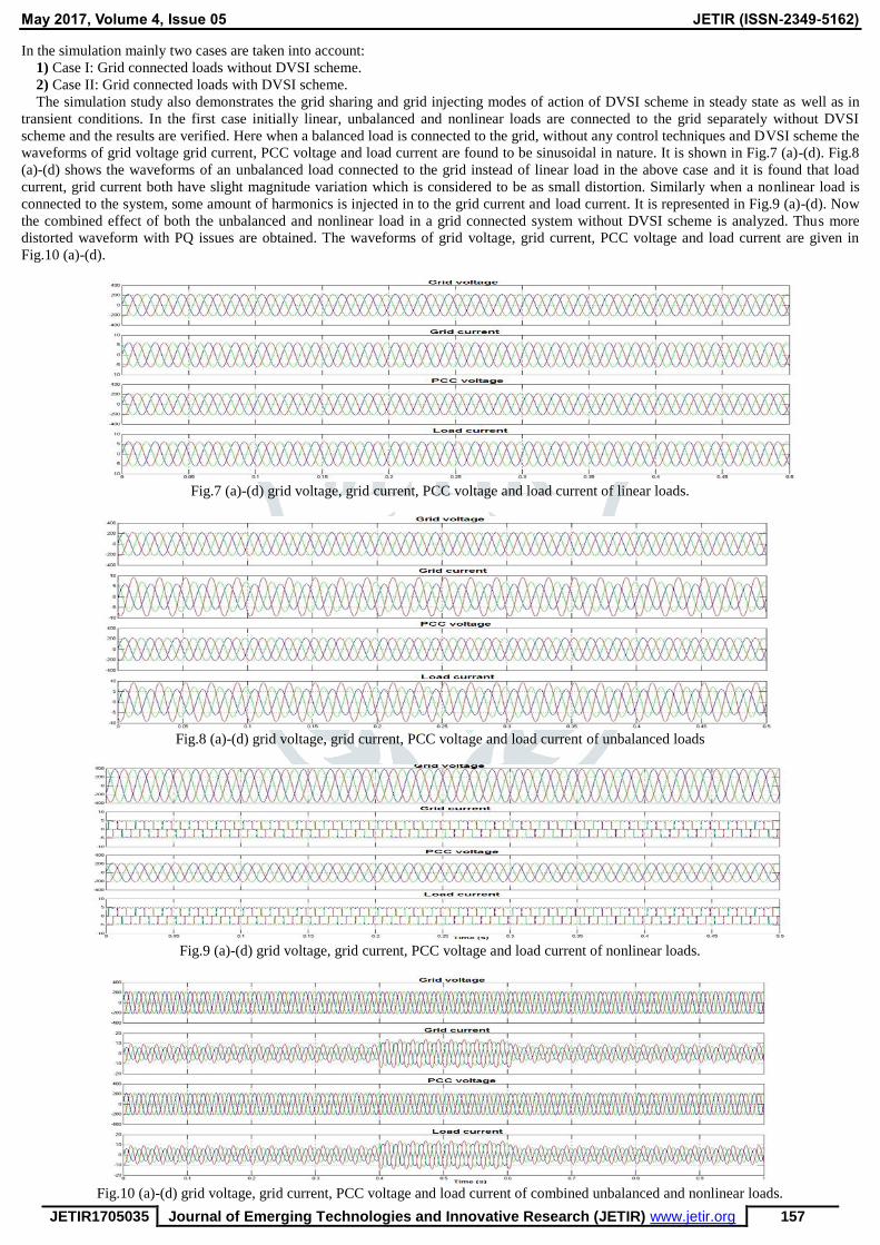
transient conditions. In the first case initially linear, unbalanced and nonlinear loads are connected to the grid separately without DVSI
scheme and the results are verified. Here when a balanced load is connected to the grid, without any control techniques and DVSI scheme the
waveforms of grid voltage grid current, PCC voltage and load current are found to be sinusoidal in nature. It is shown in Fig.7 (a)-(d). Fig.8
(a)-(d) shows the waveforms of an unbalanced load connected to the grid instead of linear load in the above case and it is found that load
current, grid current both have slight magnitude variation which is considered to be as small distortion. Similarly when a nonlinear load is
connected to the system, some amount of harmonics is injected in to the grid current and load current. It is represented in Fig.9 (a)-(d). Now
the combined effect of both the unbalanced and nonlinear load in a grid connected system without DVSI scheme is analyzed. Thus more
distorted waveform with PQ issues are obtained. The waveforms of grid voltage, grid current, PCC voltage and load current are given in
Fig.10 (a)-(d).
Fig.7 (a)-(d) grid voltage, grid current, PCC voltage and load current of linear loads.
Fig.8 (a)-(d) grid voltage, grid current, PCC voltage and load current of unbalanced loads
Fig.9 (a)-(d) grid voltage, grid current, PCC voltage and load current of nonlinear loads.
Fig.10 (a)-(d) grid voltage, grid current, PCC voltage and load current of combined unbalanced and nonlinear loads.

May 2017, Volume 4, Issue 05 JETIR (ISSN-2349-5162)
JETIR1705035 Journal of Emerging Technologies and Innovative Research (JETIR) www.jetir.org 158
In order to overcome these problems we have to introduce the DVSI scheme with HBCC technique. With the proposed scheme the same
procedure is repeated for nonlinear unbalanced and combined effect of these loads in the second case. The loads are connected separately to
the grid initially and the results are verified. The waveforms are found to be more smoothen than the first case. That is the harmonics and
voltage magnitude changes are reduced in the grid current waveform to a certain extend. Here the grid current, load current, MVSI current
and AVSI current are shown in Fig.11, 12 and 13 (a)-(d) for unbalanced load, nonlinear load and the combination of both loads.
Fig. 11 (a)-(d) grid current, load current, MVSI current and AVSI current of unbalanced loads.
Fig. 12 (a)-(d) grid current, load current, MVSI current and AVSI current of nonlinear load.
Fig.13 (a)-(d) grid current, load current, MVSI current and AVSI current of combined nonlinear and unbalanced load.
Fig. 14(a)–(d) represents active power demanded by load ( lP ), active power supplied by grid ( gp ), active power supplied by
MVSI ( gP ), and active power supplied by AVSI ( xp ), respectively. It can be observed that, from t = 0.1 to 0.4 s, MVSI is generating 4 kW
power and the load demand is 6 kW. Therefore, the remaining load active power (2 kW) is drawn from the grid. During this period, the

May 2017, Volume 4, Issue 05 JETIR (ISSN-2349-5162)
JETIR1705035 Journal of Emerging Technologies and Innovative Research (JETIR) www.jetir.org 159
microgrid is operating in grid sharing mode. At t = 0.4 s, the microgrid power is increased to 7 kW, which is more than the load demand of 6
kW. This microgrid power change is considered
to show the change of operation of MVSI from grid sharing to grid injecting mode. Now, the excess power of 1 kW is injected to the grid
and hence, the power drawn from grid is
shown as negative. Fig. 15(a)–(c) shows the load reactive power ( lQ ), reactive power supplied by AVSI ( xQ ), and reactive power supplied
by MVSI ( gQ ), respectively. It shows that total load reactive power is supplied by AVSI, as expected.
Fig.14 Active power sharing : (a) load active power, (b) active power supplied by grid, (c) active power supplied by MVSI , and (d) active
power supplied by AVSI.
Fig.15 Reactive power sharing: (a) load reactive power, (b) reactive power supplied by MVSI, reactive power supplied by AVSI
All these simulation results presented above demonstrate the feasibility of DVSI for the load compensation as well as power injection
from DG units in a microgrid.
VI. CONCLUSION
This paper proposes a DVSI scheme to improve the power quality of the microgrid system and thus to reduce the effect of harmonic
caused due to nonlinear and unbalanced loads in a grid connected DG system, which uses an hysteresis band current controller (HBCC). The
analysis and design of the proposed scheme were presented in detail. The DVSI is designed such that along with the proposed control
algorithm it is used to function as a power quality compensator with the features of reactive power compensation, load balancing, and
mitigation of current harmonics generated by the nonlinear and unbalanced loads at the PCC. Thus the system is considered to be more
dependable when compared to a single inverter with multifunctional capabilities. The proposed controller provides a very fast dynamic
response, simplicity in implementation and peak current limiting capacity. The effectiveness of the proposed control strategy is verified
through Matlab simulations. The simulation result shows that the current unbalance, current harmonics and load reactive power, due to
unbalanced and non-linear load connected to the PCC, are compensated effectively using the two inverters in a way that the grid side
currents are always maintained as balanced and sinusoidal. Moreover, by using the control method it is easy to operate DVSI in grid sharing
and grid injecting modes.
May 2017, Volume 4, Issue 05 JETIR (ISSN-2349-5162)
JETIR1705035 Journal of Emerging Technologies and Innovative Research (JETIR) www.jetir.org 160
REFERENCES
[1] A. Kahrobaeian and Y.-R. Mohamed, ―Interactive distributed generation interface for flexible micro-grid operation in smart
distribution systems,‖ IEEE Trans. Sustain. Energy, vol. 3, no. 2, pp. 295–305, Apr. 2012
[2] N. R. Tummuru, M. K. Mishra, and S. Srinivas, ―Multifunctional VSC controlled microgrid using instantaneous symmetrical
components theory,‖ IEEE Trans. Sustain. Energy, vol. 5, no. 1, pp. 313–322, Jan. 2014.
[3] Y. Zhang, N. Gatsis, and G. Giannakis, ―Robust energy management for microgrids with high-penetration renewables,‖ IEEE Trans.
Sustain. Energy, vol. 4, no. 4, pp. 944–953, Oct. 2013.
[4] R. Majumder, A. Ghosh, G. Ledwich, and F. Zare, ―Load sharing and power quality enhanced operation of a distributed microgrid,‖
IET Renewable Power Gener., vol. 3, no. 2, pp. 109–119, Jun. 2009.
[5] J. Guerrero, P. C. Loh, T.-L. Lee, and M. Chandorkar, ―Advanced control architectures for intelligent microgrids—Part II: Power
quality, energy storage, and ac/dc microgrids,‖ IEEE Trans. Ind. Electron., vol. 60, no. 4, pp. 1263–1270, Dec. 2013.
[6] Y. Li, D. Vilathgamuwa, and P. C. Loh, ―Microgrid power quality enhancement using a three-phase four-wire grid-interfacing
compensator,‖ IEEE Trans. Ind. Appl., vol. 41, no. 6, pp. 1707–1719, Nov. 2005.
[7] M. Schonardie, R. Coelho, R. Schweitzer, and D. Martins, ―Control of the active and reactive power using dq0 transformation in a
three-phase grid-connected PV system,‖ in Proc. IEEE Int. Symp. Ind. Electron., May 2012, pp. 264–269.
[8] R. S. Bajpai and R. Gupta, ―Voltage and power flow control of grid connected wind generation system using DSTATCOM,‖ in
Proc. IEEE Power Energy Soc. Gen. Meeting—Convers. Del. Elect. Energy 21st Century, Jul. 2008, pp. 1–6.
[9] M. Singh, V. Khadkikar, A. Chandra, and R. Varma, ―Grid interconnection of renewable energy sources at the distribution level with
power-quality improvement features,‖ IEEE Trans. Power Del., vol. 26, no. 1, pp. 307–315, Jan. 2011.
[10] H.-G. Yeh, D. Gayme, and S. Low, ―Adaptive VAR control for distribution circuits with photovoltaic generators,‖ IEEE Trans.
Power Syst., vol. 27, no. 3, pp. 1656–1663, Aug. 2012.
[11] C. Demoulias, ―A new simple analytical method for calculating the optimum inverter size in grid-connected PV plants,‖ Electr.
Power Syst. Res., vol. 80, no. 10, pp. 1197–1204, 2010.
[12] R. Tonkoski, D. Turcotte, and T. H. M. EL-Fouly, ―Impact of high PV penetration on voltage profiles in residential neighborhoods,‖
IEEE Trans. Sustain. Energy, vol. 3, no. 3, pp. 518–527, Jul. 2012.
[13] X. Yu and A. Khambadkone, ―Reliability analysis and cost optimization of parallel-inverter system,‖ IEEE Trans. Ind. Electron.,
vol. 59, no. 10, pp. 3881–3889, Oct. 2012.
[14] M. K. Mishra and K. Karthikeyan, ―Design and analysis of voltage source inverter for active compensators to compensate
unbalanced and nonlinear loads,‖ in Proc. IEEE Int. Power Eng. Conf., 2007, pp. 649–654.
[15] A. Ghosh and A. Joshi, ―A new approach to load balancing and power factor correction in power distribution system,‖ IEEE Trans.
Power Del., vol. 15, no. 1, pp. 417–422, Jan. 2000.