
Maximum Ratings - EVER-STAR DATArectifier,BRC,Inverter, NTC Very Compact housing, easy to route...
24
V23990-P763-A-PM datasheet flow PIM 2 3rd 600 V / 50 A ● 3~rectifier,BRC,Inverter, NTC ● Very Compact housing, easy to route ● IGBT3/ EmCon3 technology for low saturation losses and improved EMC behavior ● Motor Drives ● Power Generation ● V23990-P763-A-PM Tj=25°C, unless otherwise specified Parameter Symbol Value Unit Repetitive peak reverse voltage V RRM 1600 V T h =80°C 80 T c =80°C 80 T h =80°C 95 T c =80°C 144 Maximum Junction Temperature T j max 150 °C Inverter IGBT T h =80°C 60 T c =80°C 75 T h =80°C 115 T c =80°C 175 t SC T j ≤150°C 6 µs V CC V GE =15V 360 V 175 100 Input Rectifier Diode A W t p =10ms T j =T j max T j =T j max t p limited by T j max Maximum Junction Temperature Power dissipation V GE T j max P tot Short circuit ratings Gate-emitter peak voltage A V °C V A Types I2t-value Maximum Ratings I FAV A 2 s I FSM Condition DC current Forward current Surge forward current 700 P tot Power dissipation I 2 t 2450 T j =25°C T j =T j max Features flow 2 housing Target Applications Schematic Collector-emitter break down voltage Repetitive peak collector current DC collector current V CE I Cpulse I C 600 ±20 W A copyright Vincotech 1 23 Dec 2014 / Revision: 4
Transcript of Maximum Ratings - EVER-STAR DATArectifier,BRC,Inverter, NTC Very Compact housing, easy to route...

V23990-P763-A-PMdatasheet
flowPIM 2 3rd 600 V / 50 A
3~rectifier,BRC,Inverter, NTC
Very Compact housing, easy to route
IGBT3/ EmCon3 technology for low saturation
losses and improved EMC behavior
Motor Drives
Power Generation
V23990-P763-A-PM
Tj=25°C, unless otherwise specified
Parameter Symbol Value Unit
Repetitive peak reverse voltage VRRM 1600 V
Th=80°C 80
Tc=80°C 80
Th=80°C 95
Tc=80°C 144
Maximum Junction Temperature Tjmax 150 °C
Inverter IGBT
Th=80°C 60
Tc=80°C 75
Th=80°C 115
Tc=80°C 175
tSC Tj≤150°C 6 µs
VCC VGE=15V 360 V
175
100
Input Rectifier Diode
A
W
tp=10ms
Tj=Tjmax
Tj=Tjmax
tp limited by Tjmax
Maximum Junction Temperature
Power dissipation
VGE
Tjmax
Ptot
Short circuit ratings
Gate-emitter peak voltage
A
V
°C
V
A
Types
I2t-value
Maximum Ratings
IFAV
A2s
IFSM
Condition
DC currentForward current
Surge forward current 700
PtotPower dissipation
I2t 2450
Tj=25°C
Tj=Tjmax
Features flow2 housing
Target Applications Schematic
Collector-emitter break down voltage
Repetitive peak collector current
DC collector current
VCE
ICpulse
IC
600
±20
W
A
copyright Vincotech 1 23 Dec 2014 / Revision: 4

V23990-P763-A-PMdatasheet
Tj=25°C, unless otherwise specified
Parameter Symbol Value Unit
Maximum Ratings
Condition
Inverter FWD
Th=80°C 52
Tc=80°C 70
Th=80°C 85
Tc=80°C 129
Brake IGBT
Th=80°C 30
Tc=80°C 30
Th=80°C 84
Tc=80°C 128
tSC Tj≤150°C 6 µs
VCC VGE=15V 360 V
Brake Inverse Diode
Th=80°C 15
Tc=80°C 15
Th=80°C 54
Tc=80°C 82
Brake FWD
Th=80°C 28
Tc=80°C 30
Th=80°C 51
Tc=80°C 78
Thermal properties
40
600
175
175
100
600
90
600
175
TopOperation temperature under switching condition -40…+Tjmax-25 °C
Storage temperature Tstg -40…+125 °C
°CMaximum Junction Temperature Tjmax 175
WPower dissipation Ptot
DC forward current
A
Tj=Tjmax
tp limited by Tjmax
AIF Tj=Tjmax
VRRMPeak Repetitive Reverse Voltage
Maximum Junction Temperature
IFRM
Tjmax
Repetitive peak forward current
VCE
IC
Power dissipation Ptot Tj=Tjmax
Tj=TjmaxDC forward current IF
Repetitive peak forward current IFRM
W
A
W
40
°C
V
A
VRRM
Peak Repetitive Reverse Voltage
Repetitive peak forward current IFRM A
ATj=Tjmax
VGE
V
°C
DC collector current
Power dissipation
Collector-emitter break down voltage
Repetitive peak collector current
V
A
°C
W
A
V
V
Tj=Tjmax
±20
600
Tj=Tjmax
VRRM
DC forward current
Tjmax
tp limited by Tjmax
Ptot
ICpuls
Maximum Junction Temperature
Short circuit ratings
Gate-emitter peak voltage
IF
tp limited by Tjmax
tp limited by Tjmax
Maximum Junction Temperature Tjmax
PtotBrake Inverse Diode Tj=Tjmax
Peak Repetitive Reverse Voltage
copyright Vincotech 2 23 Dec 2014 / Revision: 4
V23990-P763-A-PMdatasheet
Tj=25°C, unless otherwise specified
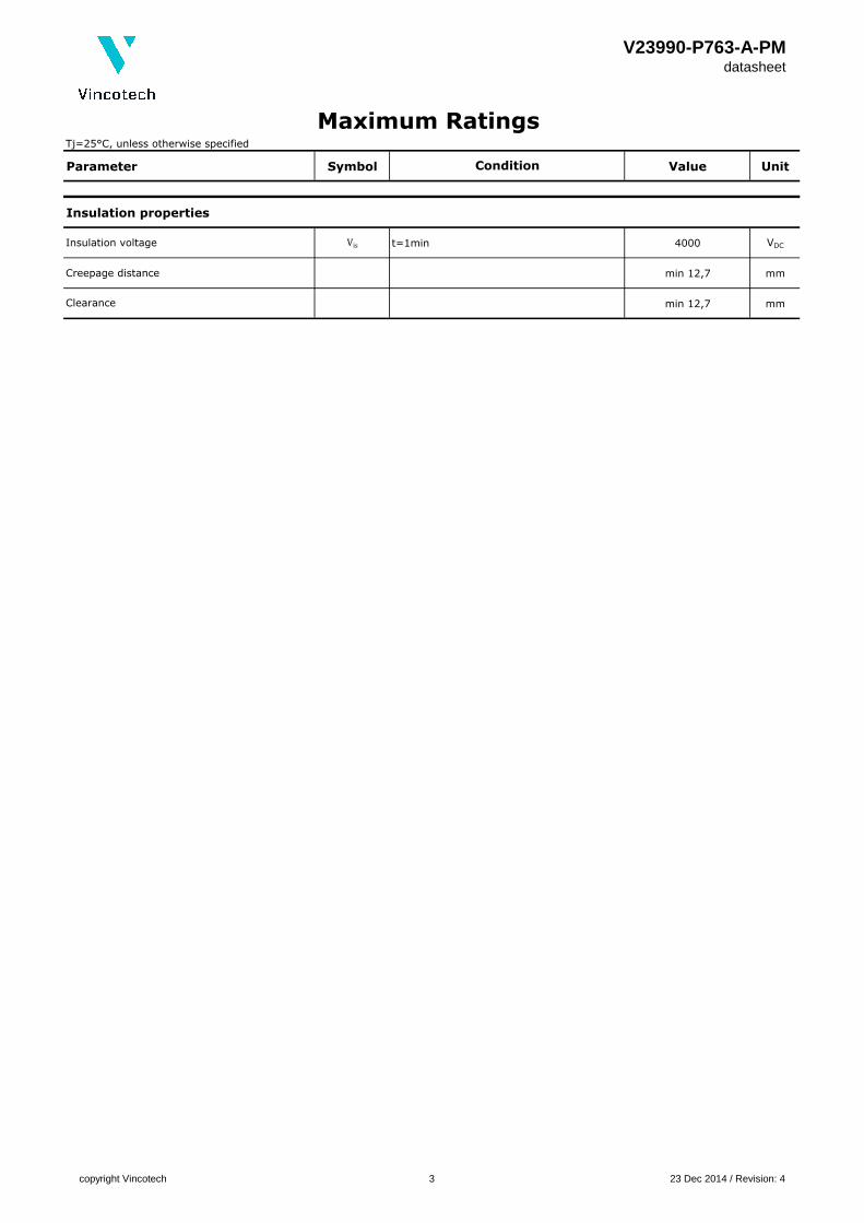
Parameter Symbol Value Unit
Maximum Ratings
Condition
Insulation properties
Vis t=1min 4000 VDC
min 12,7 mm
min 12,7 mmClearance
Insulation voltage
Creepage distance
copyright Vincotech 3 23 Dec 2014 / Revision: 4

V23990-P763-A-PMdatasheet
Parameter Symbol Unit
VGE [V] or
VGS [V]
Vr [V] or
VCE [V] or
VDS [V]
IC [A] or
IF [A] or
ID [A]
Tj Min Typ Max
Tj=25°C 1,11 1,7
Tj=125°C 1,04
Tj=25°C 0,91
Tj=125°C 0,78
Tj=25°C 0,004
Tj=125°C 0,005
Tj=25°C 0,05
Tj=125°C 1,1
Thermal resistance chip to heatsink RthJH 0,74
Thermal resistance chip to case RthJC 0,49
Tj=25°C 5 5,8 6,5
Tj=150°C
Tj=25°C 1,5 2,1
Tj=150°C 1,7
Tj=25°C 0,35
Tj=150°C
Tj=25°C 700
Tj=150°C
Tj=25°C 105
Tj=150°C 106
Tj=25°C 13
Tj=150°C 17
Tj=25°C 161
Tj=150°C 188
Tj=25°C 105
Tj=150°C 126
Tj=25°C 0,49
Tj=150°C 0,72
Tj=25°C 1,27
Tj=150°C 1,81
Thermal resistance chip to heatsink RthJH 0,82
Thermal resistance chip to case RthJC 0,54
Coupled thermal resistance transistor-transistor RthJHT-T 0,12
Coupled thermal resistance diode-transistor RthJHD-T 0,2
Tj=25°C 1,42 2,1
Tj=150°C 1,29
Tj=25°C 52
Tj=150°C 76,8
Tj=25°C 118
Tj=150°C 146
Tj=25°C 2,06
Tj=150°C 4,37
di(rec)max Tj=25°C 3668
/dt Tj=150°C 3903
Tj=25°C 0,53
Tj=150°C 0,99
Thermal resistance chip to heatsink RthJH 1,12
Thermal resistance chip to case RthJC 0,74
Coupled thermal resistance transistor-diode RthJHT-D 0,18
mWs
Ω
A
V
µC
K/W
K/W
pF
ns
mWs
V
90
200
310
3140
none
Tj=25°C
td(off)
td(on)
Rgon=8 Ω
Eoff
Thermal grease
thickness≤50µm
λ = 0,61 W/m·K
Crss
tr
f=1MHz 0
±15
1500
50
0,0008
300±15
Collector-emitter saturation voltage
Turn-on energy loss per pulse
Turn-off energy loss per pulse
Inverter FWD
ns
0
Tj=25°C25
nC
50Rgoff=8 Ω
Reverse current
Thermal grease
thickness≤50µm
λ = 0,61 W/m·K
K/W
V
V
Ω
mAIr
Characteristic Values
Forward voltage
Threshold voltage (for power loss calc. only)
Slope resistance (for power loss calc. only)
VF
Vto
rt
Input Rectifier Diode
Conditions Value
Fall time
Turn-off delay time
Turn-on delay time
Rise time
Gate-emitter leakage current
Integrated Gate resistor
Inverter IGBT
Gate emitter threshold voltage
Collector-emitter cut-off current incl. Diode
Coss
Rgint
IGES
tf
Eon
VCE(sat)
ICES
VGE(th)
50Rgon=8 Ω
Thermal grease
thickness≤50µm
λ = 0,61 W/m·K
±15Reverse recovered charge
Peak reverse recovery current
Reverse recovered energy Erec
Diode forward voltage
Qrr
trrReverse recovery time
VF
Peak rate of fall of recovery current
Input capacitance
Output capacitance
Reverse transfer capacitance
QGate
Cies
Gate charge
50
IRRM
20
15
VCE=VGE
0
480 50
600
50
300
mA
V
nA
A/µs
copyright Vincotech 4 23 Dec 2014 / Revision: 4

V23990-P763-A-PMdatasheet
Parameter Symbol Unit
VGE [V] or
VGS [V]
Vr [V] or
VCE [V] or
VDS [V]
IC [A] or
IF [A] or
ID [A]
Tj Min Typ Max
Characteristic Values
Conditions Value
Tj=25°C 5 5,8 6,5
Tj=150°C
Tj=25°C 1,5 2
Tj=150°C 1,77
Tj=25°C 0,14
Tj=150°C
Tj=25°C 400
Tj=150°C
Tj=25°C 96
Tj=150°C 98
Tj=25°C 14
Tj=150°C 18
Tj=25°C 141
Tj=150°C 170
Tj=25°C 103
Tj=150°C 121
Tj=25°C 0,38
Tj=150°C 0,51
Tj=25°C 0,71
Tj=150°C 0,98
Thermal resistance chip to heatsink RthJH 1,13
Thermal resistance chip to case RthJC 0,74
Tj=25°C 1,2 1,85 2,1
Tj=150°C 1,88
Thermal resistance chip to heatsink RthJH 1,77 K/W
Thermal resistance chip to case RthJC 1,17 K/W
Tj=25°C 1,66 2,1
Tj=150°C 1,6
Tj=25°C 140
Tj=150°C
Tj=25°C 30
Tj=150°C 33
Tj=25°C 22
Tj=150°C 146
Tj=25°C 0,47
Tj=150°C 1,81
di(rec)max Tj=25°C 4805
/dt Tj=150°C 2381
Tj=25°C 0,21
Tj=150°C 0,42
Thermal resistance chip to heatsink RthJH 1,82
Thermal resistance chip to case RthJC 1,20
20,9 22 23,1
50
Tj=25°C
Tj=25°C
Tc=100°C
Tj=25°C
25
30480
600
300
300
20
10
300 30
±15
±15
0
30
Thermal grease
thickness≤50µm
λ = 0,61 W/m·K
±15Rgon=16 Ω
Peak rate of fall of recovery current
Brake FWD
IRRM
±15
Diode forward voltage
Reverse leakage current
Tj=25°C
Tj=25°C0f=1MHz
mA
nA
mWs
VGE(th) VCE=VGE
15
Brake IGBT
Collector-emitter saturation voltage VCE(sat)
Rgon=16 Ω
Rgoff=16 Ω
20
Thermal grease
thickness≤50µm
λ = 0,61 W/m·K
Rated resistance R25 kΩTol. ±5%
Thermistor
Deviation of R100 DR/R R100=1486.1Ω %/K
B-value B(25/100) K
Power dissipation given Epcos-Typ P mW
Tol. ±3%
mWs
µC
V
µA
ns
A/µs
A
Gate emitter threshold voltage
Turn-on delay time
Rgint
td(on)
Integrated Gate resistor
ICES
IGES
Collector-emitter cut-off incl diode
Gate-emitter leakage current
Turn-off energy loss per pulse
V
167
K/W
nC
Thermal grease
thickness≤50µm
λ = 0,61 W/m·K
Turn-on energy loss per pulse Eon
Reverse recovery energy
VF
Ir
trr
Qrr
Erec
Reverse recovery time
Reverse recovered charge
Peak reverse recovery current
0
VF
Reverse transfer capacitance
QGate
Brake Inverse Diode
Gate charge
Diode forward voltage
Rise time
Turn-off delay time td(off)
tfFall time
tr
Input capacitance
Output capacitance
Crss
Cies
Coss
30
Eoff
30
0,00043
none
2,9
108
1630
210
4000
K/W
pF
ns
Ω
V
V
copyright Vincotech 5 23 Dec 2014 / Revision: 4

V23990-P763-A-PMdatasheet
Figure 1 Output inverter IGBT Figure 2 Output inverter IGBT
Typical output characteristics
IC = f(VCE) IC = f(VCE)
At At
tp = 250 µs tp = 250 µs
Tj = 25 °C Tj = 150 °C
VGE from 7 V to 17 V in steps of 1 V VGE from 7 V to 17 V in steps of 1 V
Figure 3 Output inverter IGBT Figure 4 Output inverter FWD
Typical transfer characteristics Typical diode forward current as
Ic = f(VGE) a function of forward voltage
IF = f(VF)
At At
tp = 250 µs tp = 250 µs
VCE = 10 V
Output Inverter
Typical output characteristics
0
25
50
75
100
125
150
0 1 2 3 4 5VCE (V)
I C (
A)
0
10
20
30
40
50
60
0 3 6 9 12V GE (V)
I C (
A)
Tj = 25°C
Tj = Tjmax-25°C
0
25
50
75
100
125
150
0 0,5 1 1,5 2 2,5 3VF (V)
I F (
A)
Tj = 25°CTj = Tjmax-25°C
0
25
50
75
100
125
150
0 1 2 3 4 5VCE (V)I C
(A
)
copyright Vincotech 6 23 Dec 2014 / Revision: 4

V23990-P763-A-PMdatasheet
Figure 5 Output inverter IGBT Figure 6 Output inverter IGBT
Typical switching energy losses Typical switching energy losses
as a function of collector current as a function of gate resistor
E = f(Ic) E = f(RG)
With an inductive load at With an inductive load at
Tj = 25/150 °C Tj = 25/150 °C
VCE = 300 V VCE = 300 V
VGE = ±15 V VGE = ±15 V
Rgon = 8 Ω IC = 50 A
Rgoff = 8 Ω
Figure 7 Output inverter IGBT Figure 8 Output inverter IGBT
Typical reverse recovery energy loss Typical reverse recovery energy loss
as a function of collector current as a function of gate resistor
Erec = f(Ic) Erec = f(RG)
With an inductive load at With an inductive load at
Tj = 25/150 °C Tj = 25/150 °C
VCE = 300 V VCE = 300 V
VGE = ±15 V VGE = ±15 V
Rgon = 8 Ω IC = 50 A
Output Inverter
Eon
Eoff
Eon:
Eoff
0
0,5
1
1,5
2
2,5
3
0 20 40 60 80 100I C (A)
E (
mW
s)
Eoff
Eon
Eon
Eoff
0
0,5
1
1,5
2
2,5
0 8 16 24 32 40RG ( Ω )
E (
mW
s)
Erec
Erec
0
0,3
0,6
0,9
1,2
1,5
0 20 40 60 80 100I C (A)
E (
mW
s)
Erec
Erec
0
0,2
0,4
0,6
0,8
1
0 8 16 24 32 40RG ( Ω )
E (
mW
s)
25/150 25/150
25/150 25/150
copyright Vincotech 7 23 Dec 2014 / Revision: 4

V23990-P763-A-PMdatasheet
Figure 9 Output inverter IGBT Figure 10 Output inverter IGBT
Typical switching times as a Typical switching times as a
function of collector current function of gate resistor
t = f(IC) t = f(RG)
With an inductive load at With an inductive load at
Tj = 150 °C Tj = 150 °C
VCE = 300 V VCE = 300 V
VGE = ±15 V VGE = ±15 V
Rgon = 8 Ω IC = 50 A
Rgoff = 8 Ω
Figure 11 Output inverter FWD Figure 12 Output inverter FWD
Typical reverse recovery time as a Typical reverse recovery time as a
function of collector current function of IGBT turn on gate resistor
trr = f(Ic) trr = f(Rgon)
At At
Tj = 25/150 °C Tj = 25/150 °C
VCE = 300 V VR = 300 V
VGE = ±15 V IF = 50 A
Rgon = 8 Ω VGE = ±15 V
Output Inverter
tdoff
tf
tdon
tr
0,001
0,01
0,1
1
0 20 40 60 80 100I C (A)
t (µs
)
trr
trr
0
0,05
0,1
0,15
0,2
0,25
0,3
0,35
0 8 16 24 32 40RGon ( ΩΩΩΩ )
t rr(
µs)
tdoff
tf
tdon
tr
0,001
0,01
0,1
1
0 8 16 24 32 40RG ( ΩΩΩΩ )
t (µs
)
trr
trr
0
0,04
0,08
0,12
0,16
0 20 40 60 80 100I C (A)
t rr(
µs)
25/150 25/150
copyright Vincotech 8 23 Dec 2014 / Revision: 4

V23990-P763-A-PMdatasheet
Figure 13 Output inverter FWD Figure 14 Output inverter FWD
Typical reverse recovery charge as a Typical reverse recovery charge as a
function of collector current function of IGBT turn on gate resistor
Qrr = f(Ic) Qrr = f(Rgon)
At
At At
Tj = 25/150 °C Tj = 25/150 °C
VCE = 300 V VR = 300 V
VGE = ±15 V IF = 50 A
Rgon = 8 Ω VGE = ±15 V
Figure 15 Output inverter FWD Figure 16 Output inverter FWD
Typical reverse recovery current as a Typical reverse recovery current as a
function of collector current function of IGBT turn on gate resistor
IRRM = f(Ic) IRRM = f(Rgon)
At At
Tj = 25/150 °C Tj = 25/150 °C
VCE = 300 V VR = 300 V
VGE = ±15 V IF = 50 A
Rgon = 8 Ω VGE = ±15 V
Output Inverter
IRRM
IRRM
0
20
40
60
80
100
120
0 8 16 24 32 40RGon( ΩΩΩΩ )
I RR
M (
A)
Qrr
Qrr
0
1
2
3
4
5
0 8 16 24 32 40RGon (Ω)
Qrr (
µC)
IRRM
IRRM
0
20
40
60
80
100
0 20 40 60 80 100I C (A)
I RR
M (
A)
Qrr
Qrr
0
1
2
3
4
5
6
0 20 40 60 80 100I C (A)
Qrr (
µC)
25/150 25/150
25/150 25/150
copyright Vincotech 9 23 Dec 2014 / Revision: 4

V23990-P763-A-PMdatasheet
Figure 17 Output inverter FWD Figure 18 Output inverter FWD
Typical rate of fall of forward Typical rate of fall of forward
and reverse recovery current as a and reverse recovery current as a
function of collector current function of IGBT turn on gate resistor
dI0/dt,dIrec/dt = f(Ic) dI0/dt,dIrec/dt = f(Rgon)
At At
Tj = 25/150 °C Tj = 25/150 °C
VCE = 300 V VR = 300 V
VGE = ±15 V IF = 50 A
Rgon = 8 Ω VGE = ±15 V
Figure 19 Output inverter IGBT Figure 20 Output inverter FWD
IGBT transient thermal impedance FWD transient thermal impedance
as a function of pulse width as a function of pulse width
ZthJH = f(tp) ZthJH = f(tp)
At At
D = tp / T D = tp / T
RthJH = 0,823 K/W RthJH = 0,94 K/W RthJH = 1,12 K/W RthJH = 1,12 K/W
Single device heated AlI devices heated Single device heated AlI devices heated
IGBT thermal model values FWD thermal model values
R (K/W) Tau (s) R (K/W) R (K/W) Tau (s) R (K/W)
0,02 9,2E+00 0,14 0,02 9,2E+00 0,02
0,08 1,2E+00 0,08 0,08 1,2E+00 0,08
0,19 1,6E-01 0,19 0,22 1,3E-01 0,22
0,38 3,7E-02 0,38 0,49 2,8E-02 0,49
0,09 7,1E-03 0,09 0,20 5,9E-03 0,20
0,06 5,8E-04 0,06 0,11 5,5E-04 0,11
Output Inverter
t p (s)
Zth
JH (
K/W
)
101
100
10-1
10-2
10-4 10-3 10-2 10-1 100 1011010-5
D = 0,5 0,2 0,1 0,05 0,02 0,01 0,005 0.000
t p (s)
Zth
JH (
K/W
)
101
100
10-1
10-2
10-4 10-3 10-2 10-1 100 1011010-5
D = 0,5 0,2 0,1 0,05 0,02 0,01 0,005 0.000
dI0/dt
dIrec/dt
0
1000
2000
3000
4000
5000
6000
7000
8000
9000
0 8 16 24 32 40RGon (Ω)
dire
c / d
t (A
/ µs)
dI0/dt
dIrec/dt
0
1000
2000
3000
4000
5000
0 20 40 60 80 100I C (A)
dire
c / d
t (A
/ µs)
25/150 25/150
copyright Vincotech 10 23 Dec 2014 / Revision: 4

V23990-P763-A-PMdatasheet
Figure 21 Output inverter IGBT Figure 22 Output inverter IGBT
Power dissipation as a Collector current as a
function of heatsink temperature function of heatsink temperature
Ptot = f(Th) IC = f(Th)
At At
Tj = 175 °C single heating Tj = 175 °C
overall heating VGE = 15 V
Figure 23 Output inverter FWD Figure 24 Output inverter FWD
Power dissipation as a Forward current as a
function of heatsink temperature function of heatsink temperature
Ptot = f(Th) IF = f(Th)
At At
Tj = 175 °C Tj = 175 °C
Output Inverter
0
50
100
150
200
250
0 50 100 150 200Th (o C)
Pto
t (W
)
0
20
40
60
80
0 50 100 150 200Th (o C)
I C (A
)
0
40
80
120
160
0 50 100 150 200Th (o C)
Pto
t (W
)
0
20
40
60
80
0 50 100 150 200Th (o C)
I F (A
)
copyright Vincotech 11 23 Dec 2014 / Revision: 4

V23990-P763-A-PMdatasheet
Figure 25 Output inverter IGBT Figure 26 Output inverter IGBT
Safe operating area as a function Gate voltage vs Gate charge
of collector-emitter voltage
IC = f(VCE) VGE = f(Qg)
At At
D = single pulse IC = 50 A
Th = 80 ºC
VGE = ±15 V
Tj = Tjmax ºC
Output Inverter
V CE (V)
I C (A
)
103
100
10-1
101
102
101 102
100uS
1mS
10mS
100mS
DC
100103
10uS
0
3
6
9
12
15
18
0 50 100 150 200 250 300 350 400Qg (nC)
VG
E (
V)
120V
480V
copyright Vincotech 12 23 Dec 2014 / Revision: 4

V23990-P763-A-PMdatasheet
Figure 1 Brake IGBT Figure 2 Brake IGBT
Typical output characteristics Typical output characteristics
IC = f(VCE) IC = f(VCE)
At At
tp = 250 µs tp = 250 µs
Tj = 25 °C Tj = 150 °C
VGE from 7 V to 17 V in steps of 1 V VGE from 7 V to 17 V in steps of 1 V
Figure 3 Brake IGBT Figure 4 Brake FWD
Typical transfer characteristics Typical diode forward current as
IC = f(VGE) a function of forward voltage
IF = f(VF)
At At
tp = 250 µs tp = 250 µs
VCE = 10 V
Brake
0
15
30
45
60
75
90
0 1 2 3 4 5V CE (V)
I C (
A)
0
5
10
15
20
25
30
0 2 4 6 8 10 12V GE (V)
I C (
A)
Tj = 25°C
Tj = Tjmax-25°C
0
10
20
30
40
50
60
0 0,5 1 1,5 2 2,5 3V F (V)
I F (
A)
Tj = 25°C
Tj = Tjmax-25°C
0
15
30
45
60
75
90
0 1 2 3 4 5V CE (V)I C
(A
)
copyright Vincotech 13 23 Dec 2014 / Revision: 4
V23990-P763-A-PMdatasheet
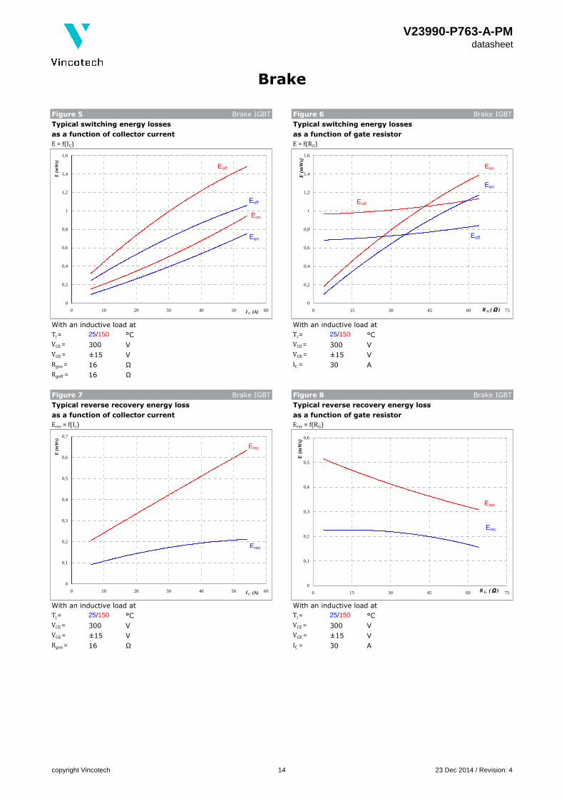
Figure 5 Brake IGBT Figure 6 Brake IGBT
Typical switching energy losses Typical switching energy losses
as a function of collector current as a function of gate resistor
E = f(IC) E = f(RG)
With an inductive load at With an inductive load at
Tj = 25/150 °C Tj = 25/150 °C
VCE = 300 V VCE = 300 V
VGE = ±15 V VGE = ±15 V
Rgon = 16 Ω IC = 30 A
Rgoff = 16 Ω
Figure 7 Brake IGBT Figure 8 Brake IGBT
Typical reverse recovery energy loss Typical reverse recovery energy loss
as a function of collector current as a function of gate resistor
Erec = f(Ic) Erec = f(RG)
With an inductive load at With an inductive load at
Tj = 25/150 °C Tj = 25/150 °C
VCE = 300 V VCE = 300 V
VGE = ±15 V VGE = ±15 V
Rgon = 16 Ω IC = 30 A
Brake
Erec
Erec
0
0,1
0,2
0,3
0,4
0,5
0,6
0,7
0 10 20 30 40 50 60I C (A)
E (
mW
s)
Erec
Erec
0
0,1
0,2
0,3
0,4
0,5
0,6
0 15 30 45 60 75RG ( ΩΩΩΩ )
E (
mW
s)
Eoff
Eon
Eon
Eoff
0
0,2
0,4
0,6
0,8
1
1,2
1,4
1,6
0 10 20 30 40 50 60I C (A)
E (
mW
s)
Eoff
Eon
Eon
Eoff
0
0,2
0,4
0,6
0,8
1
1,2
1,4
1,6
0 15 30 45 60 75RG ( ΩΩΩΩ )
E (
mW
s)
25/150 25/150
25/150 25/150
copyright Vincotech 14 23 Dec 2014 / Revision: 4

V23990-P763-A-PMdatasheet
Figure 9 Brake IGBT Figure 10 Brake IGBT
Typical switching times as a Typical switching times as a
function of collector current function of gate resistor
t = f(IC) t = f(RG)
With an inductive load at With an inductive load at
Tj = 150 °C Tj = 150 °C
VCE = 300 V VCE = 300 V
VGE = ±15 V VGE = ±15 V
Rgon = 16 Ω IC = 30 A
Rgoff = 16 Ω
Figure 11 Brake IGBT Figure 12 Brake IGBT
IGBT transient thermal impedance FWD transient thermal impedance
as a function of pulse width as a function of pulse width
ZthJH = f(tp) ZthJH = f(tp)
At At
D = tp / T D = tp / T
RthJH = 1,13 K/W RthJH = 1,82 K/W
Brake
tdoff
tf
tdon
tr
0,001
0,01
0,1
1
0 10 20 30 40 50 60IC (A)
t (µs
)
tdoff
tf
tdon
tr
0,001
0,01
0,1
1
0 15 30 45 60 75RG ( ΩΩΩΩ )t (
µs)
t p (s)
Zth
JH (
K/W
)
101
100
10-1
10-2
10-4 10-3 10-2 10-1 100 101 1010-5
D = 0,5 0,2 0,1 0,05 0,02 0,01 0,005 0.000
t p (s)
Zth
JH (
K/W
)
101
100
10-1
10-2
10-4 10-3 10-2 10-1 100 101 1010-5
D = 0,5 0,2 0,1 0,05 0,02 0,01 0,005 0.000
copyright Vincotech 15 23 Dec 2014 / Revision: 4

V23990-P763-A-PMdatasheet
Figure 13 Brake IGBT Figure 14 Brake IGBT
Power dissipation as a Collector current as a
function of heatsink temperature function of heatsink temperature
Ptot = f(Th) IC = f(Th)
At At
Tj = 175 ºC Tj = 175 ºC
VGE = 15 V
Figure 15 Brake FWD Figure 16 Brake FWD
Power dissipation as a Forward current as a
function of heatsink temperature function of heatsink temperature
Ptot = f(Th) IF = f(Th)
At At
Tj = 175 ºC Tj = 175 ºC
Brake
0
25
50
75
100
125
150
175
0 50 100 150 200Th (o C)
Pto
t (W
)
0
10
20
30
40
0 50 100 150 200Th (o C)
I C (A
)
0
20
40
60
80
100
0 50 100 150 200Th (o C)
Pto
t (W
)
0
5
10
15
20
25
30
0 50 100 150 200Th (o C)
I F (A
)
copyright Vincotech 16 23 Dec 2014 / Revision: 4
V23990-P763-A-PMdatasheet
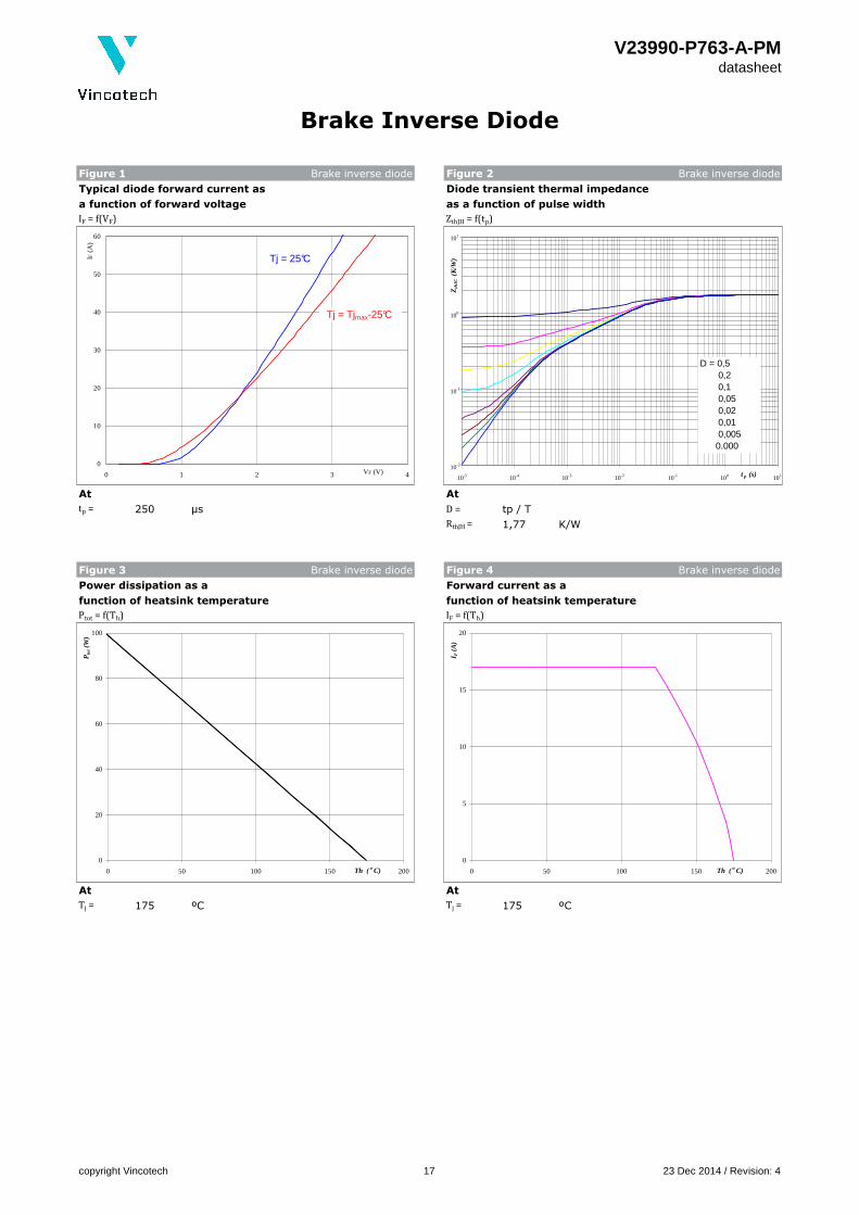
Figure 1 Brake inverse diode Figure 2 Brake inverse diode
Typical diode forward current as Diode transient thermal impedance
a function of forward voltage as a function of pulse width
IF = f(VF) ZthJH = f(tp)
At At
tp = 250 µs D = tp / T
RthJH = 1,77 K/W
Figure 3 Brake inverse diode Figure 4 Brake inverse diode
Power dissipation as a Forward current as a
function of heatsink temperature function of heatsink temperature
Ptot = f(Th) IF = f(Th)
At At
Tj = 175 ºC Tj = 175 ºC
Brake Inverse Diode
0
10
20
30
40
50
60
0 1 2 3 4VF (V)
I F (
A)
Tj = 25°C
Tj = Tjmax-25°C
t p (s)
Zth
JC (
K/W
)
101
100
10-1
10-2
10-4 10-3 10-2 10-1 100 1011010-5
D = 0,5 0,2 0,1 0,05 0,02 0,01 0,005 0.000
0
20
40
60
80
100
0 50 100 150 200Th (o C)
Pto
t (W
)
0
5
10
15
20
0 50 100 150 200Th (o C)
I F (A
)
copyright Vincotech 17 23 Dec 2014 / Revision: 4

V23990-P763-A-PMdatasheet
Figure 1 Rectifier diode Figure 2 Rectifier diode
Typical diode forward current as Diode transient thermal impedance
a function of forward voltage as a function of pulse width
IF= f(VF) ZthJH = f(tp)
At At
tp = 250 µs D = tp / T
RthJH = 0,74 K/W
Figure 3 Rectifier diode Figure 4 Rectifier diode
Power dissipation as a Forward current as a
function of heatsink temperature function of heatsink temperature
Ptot = f(Th) IF = f(Th)
At At
Tj = 150 ºC Tj = 150 ºC
Input Rectifier Bridge
0
25
50
75
100
125
150
0 0,3 0,6 0,9 1,2 1,5 1,8VF (V)
I F (
A)
Tj = 25°C
Tj = Tjmax-25°C
t p (s)
Zth
JC (
K/W
)
100
10-1
10-2
10-4 10-3 10-2 10-1 100 1011010-5
D = 0,5 0,2 0,1 0,05 0,02 0,01 0,005 0.000
0
40
80
120
160
200
240
0 30 60 90 120 150Th (o C)
Pto
t (W
)
0
20
40
60
80
0 30 60 90 120 150Th (o C)
I F (A
)
copyright Vincotech 18 23 Dec 2014 / Revision: 4

V23990-P763-A-PMdatasheet
Figure 1 Thermistor
Typical NTC characteristic
as a function of temperature
RT = f(T)
Thermistor
NTC-typical temperature characteristic
0
5000
10000
15000
20000
25000
25 50 75 100 125T (°C)
R (Ω
)
copyright Vincotech 19 23 Dec 2014 / Revision: 4

V23990-P763-A-PMdatasheet
Tj 150 °C
Rgon 8 Ω
Rgoff 8 Ω
Figure 1 Output inverter IGBT Figure 2 Output inverter IGBT
Turn-off Switching Waveforms & definition of tdoff, tEoff Turn-on Switching Waveforms & definition of tdon, tEon
(tEoff = integrating time for Eoff) (tEon = integrating time for Eon)
VGE (0%) = -15 V VGE (0%) = -15 V
VGE (100%) = 15 V VGE (100%) = 15 V
VC (100%) = 300 V VC (100%) = 300 V
IC (100%) = 50 A IC (100%) = 50 A
tdoff = 0,19 µs tdon = 0,11 µs
tEoff = 0,58 µs tEon = 0,24 µs
Figure 3 Output inverter IGBT Figure 4 Output inverter IGBT
Turn-off Switching Waveforms & definition of tf Turn-on Switching Waveforms & definition of tr
VC (100%) = 300 V VC (100%) = 300 V
IC (100%) = 50 A IC (100%) = 50 A
tf = 0,13 µs tr = 0,02 µs
Switching Definitions Output InverterGeneral conditions
=
=
=
Ic 1%
Uce 90%Uge 90%
0
20
40
60
80
100
120
-0,1 0 0,1 0,2 0,3 0,4 0,5 0,6 0,7 0,8time (µs)
%tdoff
tEoff
UCE
Ic
Uge
Ic10%
Uge10%
tdon
Uce3%
-40
0
40
80
120
160
200
240
280
2,95 3 3,05 3,1 3,15 3,2 3,25 3,3time(µs)
%Ic
Uce
tEon
Uge
fitted
Ic10%
Ic 90%
Ic 60%
Ic 40%
-20
0
20
40
60
80
100
120
0,15 0,2 0,25 0,3 0,35 0,4 0,45 0,5time (µs)
% UCE
Ic
tfIc10%
Ic90%
-20
20
60
100
140
180
220
260
3,05 3,1 3,15 3,2 3,25time(µs)
%
tr
Uce
Ic
copyright Vincotech 20 23 Dec 2014 / Revision: 4

V23990-P763-A-PMdatasheet
Figure 5 Output inverter IGBT Figure 6 Output inverter IGBT
Turn-off Switching Waveforms & definition of tEoff Turn-on Switching Waveforms & definition of tEon
Poff (100%) = 15,03 kW Pon (100%) = 15,03 kW
Eoff (100%) = 1,81 mJ Eon (100%) = 0,72 mJ
tEoff = 0,58 µs tEon = 0,24 µs
Figure 7 Output inverter FWD
Turn-off Switching Waveforms & definition of trr
Vd (100%) = 300 V
Id (100%) = 50 A
IRRM (100%) = -77 A
trr = 0,15 µs
Switching Definitions Output Inverter
Ic 1%
Uge90%
-20
0
20
40
60
80
100
120
-0,1 0,05 0,2 0,35 0,5 0,65 0,8 0,95time (µs)
%
PoffEoff
tEoff
Uce3%Uge10%
-30
0
30
60
90
120
150
2,9 3 3,1 3,2 3,3 3,4time(µs)
% Pon
Eon
tEon
IRRM10%
IRRM90%
IRRM100%
trr
-200
-160
-120
-80
-40
0
40
80
120
3,05 3,1 3,15 3,2 3,25 3,3 3,35time(µs)
%Id
Ud fitted
copyright Vincotech 21 23 Dec 2014 / Revision: 4

V23990-P763-A-PMdatasheet
Figure 8 Output inverter FWD Figure 9 Output inverter FWD
Turn-on Switching Waveforms & definition of tQrr Turn-on Switching Waveforms & definition of tErec
(tQrr = integrating time for Qrr) (tErec= integrating time for Erec)
Id (100%) = 50 A Prec (100%) = 15,03 kW
Qrr (100%) = 4,37 µC Erec (100%) = 0,99 mJ
tQint = 0,29 µs tErec = 0,29 µs
Switching Definitions Output Inverter
tQrr
-200
-100
0
100
200
2,95 3,1 3,25 3,4 3,55 3,7time(µs)
%
Id Qrr
-40
-10
20
50
80
110
140
2,95 3,15 3,35 3,55 3,75time(µs)
%
Prec
Erec
tErec
copyright Vincotech 22 23 Dec 2014 / Revision: 4

V23990-P763-A-PMdatasheet
in DataMatrix as in packaging barcode as
without thermal paste 12mm housing P760-A P760-A
Pin X Y Pin X Y
1 DC- 71,2 0 33 G 10,6 37,2
2 DC- 68,7 0 34 G 18,45 37,2
3 DC- 66,2 0 35 E 21,25 37,2
4 DC- 63,7 0 36 V 24,05 37,2
5 DC+ 55,95 0 37 V 26,55 37,2
6 DC+ 53,45 0 38 V 29,05 37,2
7 DC+ 55,95 2,8 39 W 36,1 37,2
8 DC+ 53,45 2,8 40 W 38,6 37,2
9 DC+ 48,4 0 41 W 41,1 37,2
10 DC+ 45,9 0 42 E 43,9 37,2
11 E 38,9 0 43 G 46,7 37,2
12 DC- 36,1 0 44 L1 53,7 37,2
13 G 38,9 2,8 45 L1 56,2 37,2
14 DC- 36,1 2,8 46 L1 58,7 37,2
15 DC- 31,3 0 47 L2 71,2 37,2
16 E 28,5 0 48 L2 71,2 34,7
17 DC- 31,3 2,8 49 L2 71,2 32,2
18 G 28,5 2,8 50 L3 71,2 25,2
19 R2 19,3 0 51 L3 71,2 22,7
20 R1 19,3 2,8 52 L3 71,2 20,2
21 DC+ 12,3 0 53 BrC 71,2 12,8
22 DC+ 9,8 0 54 BrC 68,7 12,8
23 DC+ 12,3 2,8 55 BrG 71,2 5,6
24 DC+ 9,8 2,8 56 BrE 71,2 2,8
25 E 2,8 0
26 DC- 0 0
27 G 2,8 2,8
28 DC- 0 2,8
29 U 0 37,2
30 U 2,5 37,2
31 U 5 37,2
32 E 7,8 37,2
V23990-P760-A-PM
Pinout
Ordering Code & Marking
Ordering Code and Marking - Outline - Pinout
Version
Outline
Ordering Code
Pin table
copyright Vincotech 23 23 Dec 2014 / Revision: 4
V23990-P763-A-PMdatasheet
DISCLAIMER
LIFE SUPPORT POLICY
As used herein:
The information given in this datasheet describes the type of component and does not represent assured
characteristics. For tested values please contact Vincotech.Vincotech reserves the right to make changes without further
notice to any products herein to improve reliability, function or design. Vincotech does not assume any liability arising
out of the application or use of any product or circuit described herein; neither does it convey any license under its
patent rights, nor the rights of others.
Vincotech products are not authorised for use as critical components in life support devices or systems without the
express written approval of Vincotech.
2. A critical component is any component of a life support device or system whose failure to perform can be reasonably
expected to cause the failure of the life support device or system, or to affect its safety or effectiveness.
1. Life support devices or systems are devices or systems which, (a) are intended for surgical implant into the body, or
(b) support or sustain life, or (c) whose failure to perform when properly used in accordance with instructions for use
provided in labelling can be reasonably expected to result in significant injury to the user.
copyright Vincotech 24 23 Dec 2014 / Revision: 4