MAX9934 High-Precision, Low-Voltage, Current-Sense ... · MAX9934 High-Precision, Low-Voltage,...
19
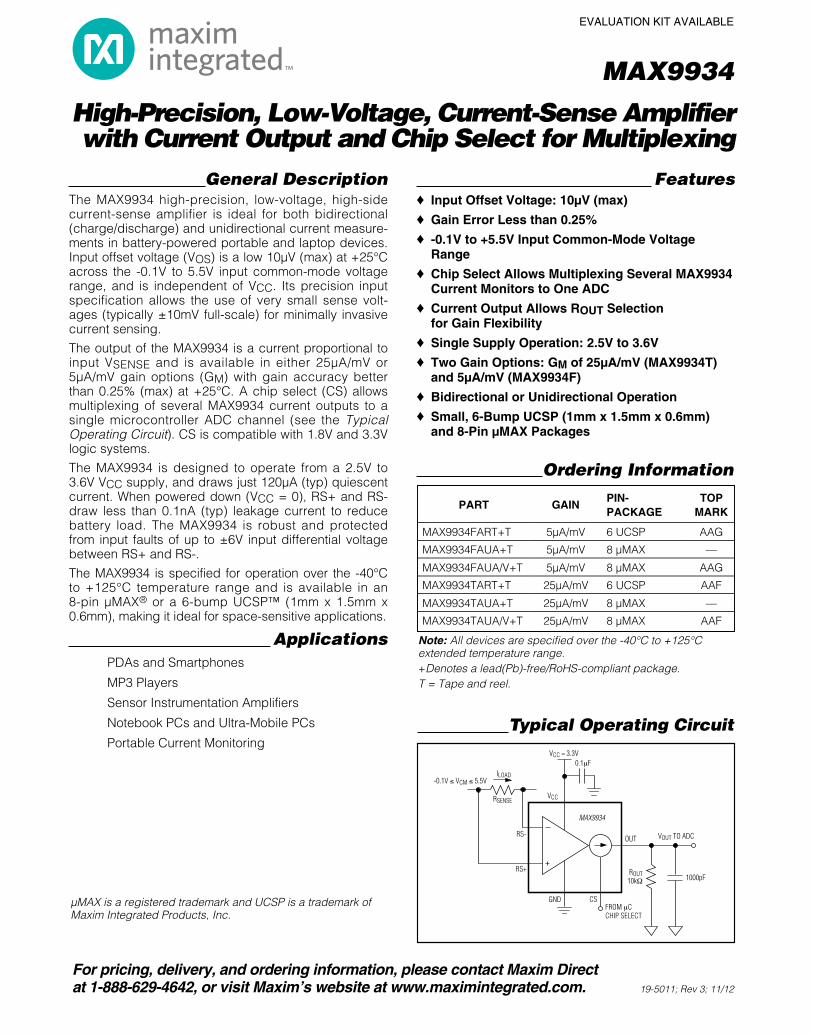
MAX9934 High-Precision, Low-Voltage, Current-Sense Amplifier with Current Output and Chip Select for Multiplexing EVALUATION KIT AVAILABLE 19-5011; Rev 3; 11/12 For pricing, delivery, and ordering information, please contact Maxim Direct at 1-888-629-4642, or visit Maxim’s website at www.maximintegrated.com. General Description The MAX9934 high-precision, low-voltage, high-side current-sense amplifier is ideal for both bidirectional (charge/discharge) and unidirectional current measure- ments in battery-powered portable and laptop devices. Input offset voltage (V OS ) is a low 10μV (max) at +25°C across the -0.1V to 5.5V input common-mode voltage range, and is independent of V CC . Its precision input specification allows the use of very small sense volt- ages (typically ±10mV full-scale) for minimally invasive current sensing. The output of the MAX9934 is a current proportional to input V SENSE and is available in either 25μA/mV or 5μA/mV gain options (G M ) with gain accuracy better than 0.25% (max) at +25°C. A chip select (CS) allows multiplexing of several MAX9934 current outputs to a single microcontroller ADC channel (see the Typical Operating Circuit). CS is compatible with 1.8V and 3.3V logic systems. The MAX9934 is designed to operate from a 2.5V to 3.6V V CC supply, and draws just 120μA (typ) quiescent current. When powered down (V CC = 0), RS+ and RS- draw less than 0.1nA (typ) leakage current to reduce battery load. The MAX9934 is robust and protected from input faults of up to ±6V input differential voltage between RS+ and RS-. The MAX9934 is specified for operation over the -40°C to +125°C temperature range and is available in an 8-pin μMAX ® or a 6-bump UCSP™ (1mm x 1.5mm x 0.6mm), making it ideal for space-sensitive applications. Applications PDAs and Smartphones MP3 Players Sensor Instrumentation Amplifiers Notebook PCs and Ultra-Mobile PCs Portable Current Monitoring Features ♦ Input Offset Voltage: 10µV (max) ♦ Gain Error Less than 0.25% ♦ -0.1V to +5.5V Input Common-Mode Voltage Range ♦ Chip Select Allows Multiplexing Several MAX9934 Current Monitors to One ADC ♦ Current Output Allows R OUT Selection for Gain Flexibility ♦ Single Supply Operation: 2.5V to 3.6V ♦ Two Gain Options: G M of 25µA/mV (MAX9934T) and 5µA/mV (MAX9934F) ♦ Bidirectional or Unidirectional Operation ♦ Small, 6-Bump UCSP (1mm x 1.5mm x 0.6mm) and 8-Pin µMAX Packages Ordering Information PART GAIN PIN- PACKAGE TOP MARK MAX9934FART+T 5μA/mV 6 UCSP AAG MAX9934FAUA+T 5μA/mV 8 μMAX — MAX9934FAUA/V+T 5μA/mV 8 μMAX AAG MAX9934TART+T 25μA/mV 6 UCSP AAF MAX9934TAUA+T 25μA/mV 8 μMAX — MAX9934TAUA/V+T 25μA/mV 8 μMAX AAF Note: All devices are specified over the -40°C to +125°C extended temperature range. +Denotes a lead(Pb)-free/RoHS-compliant package. T = Tape and reel. μMAX is a registered trademark and UCSP is a trademark of Maxim Integrated Products, Inc. ILOAD RSENSE RS- RS+ -0.1V ≤ VCM ≤ 5.5V VCC = 3.3V VCC CS GND MAX9934 OUT ROUT 10kΩ VOUT TO ADC FROM µC CHIP SELECT 1000pF 0.1µF Typical Operating Circuit
Transcript of MAX9934 High-Precision, Low-Voltage, Current-Sense ... · MAX9934 High-Precision, Low-Voltage,...
MAX9934
High-Precision, Low-Voltage, Current-Sense Amplifierwith Current Output and Chip Select for Multiplexing
EVALUATION KIT AVAILABLE
19-5011; Rev 3; 11/12
For pricing, delivery, and ordering information, please contact Maxim Directat 1-888-629-4642, or visit Maxim’s website at www.maximintegrated.com.
General DescriptionThe MAX9934 high-precision, low-voltage, high-sidecurrent-sense amplifier is ideal for both bidirectional(charge/discharge) and unidirectional current measure-ments in battery-powered portable and laptop devices.Input offset voltage (VOS) is a low 10µV (max) at +25°Cacross the -0.1V to 5.5V input common-mode voltagerange, and is independent of VCC. Its precision inputspecification allows the use of very small sense volt-ages (typically ±10mV full-scale) for minimally invasivecurrent sensing.
The output of the MAX9934 is a current proportional toinput VSENSE and is available in either 25µA/mV or5µA/mV gain options (GM) with gain accuracy betterthan 0.25% (max) at +25°C. A chip select (CS) allowsmultiplexing of several MAX9934 current outputs to asingle microcontroller ADC channel (see the TypicalOperating Circuit). CS is compatible with 1.8V and 3.3Vlogic systems.
The MAX9934 is designed to operate from a 2.5V to3.6V VCC supply, and draws just 120µA (typ) quiescentcurrent. When powered down (VCC = 0), RS+ and RS-draw less than 0.1nA (typ) leakage current to reducebattery load. The MAX9934 is robust and protectedfrom input faults of up to ±6V input differential voltagebetween RS+ and RS-.
The MAX9934 is specified for operation over the -40°Cto +125°C temperature range and is available in an 8-pin µMAX® or a 6-bump UCSP™ (1mm x 1.5mm x0.6mm), making it ideal for space-sensitive applications.
ApplicationsPDAs and Smartphones
MP3 Players
Sensor Instrumentation Amplifiers
Notebook PCs and Ultra-Mobile PCs
Portable Current Monitoring
Features Input Offset Voltage: 10µV (max)
Gain Error Less than 0.25%
-0.1V to +5.5V Input Common-Mode VoltageRange
Chip Select Allows Multiplexing Several MAX9934Current Monitors to One ADC
Current Output Allows ROUT Selectionfor Gain Flexibility
Single Supply Operation: 2.5V to 3.6V
Two Gain Options: GM of 25µA/mV (MAX9934T)and 5µA/mV (MAX9934F)
Bidirectional or Unidirectional Operation
Small, 6-Bump UCSP (1mm x 1.5mm x 0.6mm)and 8-Pin µMAX Packages
Ordering Information
PART GAINPIN-PACKAGE
TOPMARK
MAX9934FART+T 5µA/mV 6 UCSP AAG
MAX9934FAUA+T 5µA/mV 8 µMAX —
MAX9934FAUA/V+T 5µA/mV 8 µMAX AAG
MAX9934TART+T 25µA/mV 6 UCSP AAF
MAX9934TAUA+T 25µA/mV 8 µMAX —
MAX9934TAUA/V+T 25µA/mV 8 µMAX AAF
Note: All devices are specified over the -40°C to +125°Cextended temperature range.+Denotes a lead(Pb)-free/RoHS-compliant package.T = Tape and reel.
µMAX is a registered trademark and UCSP is a trademark ofMaxim Integrated Products, Inc.
ILOAD
RSENSE
RS-
RS+
-0.1V ≤ VCM ≤ 5.5V
VCC = 3.3V
VCC
CSGND
MAX9934
OUT
ROUT10kΩ
VOUT TO ADC
FROM µCCHIP SELECT
1000pF
0.1µF
Typical Operating Circuit
MAX9934High-Precision, Low-Voltage, Current-Sense Amplifierwith Current Output and Chip Select for Multiplexing
2 Maxim Integrated
ABSOLUTE MAXIMUM RATINGS
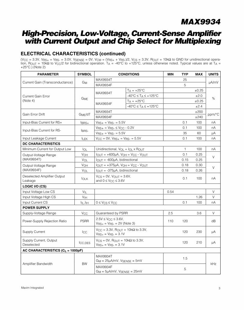
ELECTRICAL CHARACTERISTICS(VCC = 3.3V, VRS+ = VRS- = 3.0V, VSENSE = 0V, VCM = (VRS+ + VRS-)/2, VCS = 3.3V, ROUT = 10kΩ to GND for unidirectional opera-tion, ROUT = 10kΩ to VCC/2 for bidirectional operation. TA = -40°C to +125°C, unless otherwise noted. Typical values are at TA =+25°C.) (Note 2)
Stresses beyond those listed under “Absolute Maximum Ratings” may cause permanent damage to the device. These are stress ratings only, and functionaloperation of the device at these or any other conditions beyond those indicated in the operational sections of the specifications is not implied. Exposure toabsolute maximum rating conditions for extended periods may affect device reliability.
RS+, RS- to GND......................................................-0.3V to +6VVCC to GND..............................................................-0.3V to +4VCS, OUT to GND (VCC = 0, or CS < VIL)..................-0.3V to +4VOUT to GND (CS > VIH)................................-0.3V to VCC + 0.3VDifferential Input Voltage (RS+ - RS-) ....................................±6V
Output Short-Circuit Current Duration OUT to GND or VCC ...............................................Continuous
Continuous Input Current into Any Terminal.....................±20mAContinuous Power Dissipation (TA = +70°C)
8-Pin µMAX (derate multilayer 4.8mW/°Cabove +70°C).............................................................388mW
Junction-to-Ambient Thermal Resistance (θJA)(Note 1) ....................................................................206°C/W
Junction-to-Case Thermal Resistance (θJC)(Note 1) ......................................................................42°C/W
6-Bump UCSP (derate multilayer 3.9mW/°Cabove +70°C).............................................................308mW
Junction-to-Ambient Thermal Resistance (θJA)(Note 1) ....................................................................260°C/W
Operating Temperature Range .........................-40°C to +125°CJunction Temperature ......................................................+150°CStorage Temperature Range .............................-65°C to +160°CLead Temperature (µMAX only, soldering, 10s) ..............+300°CSoldering Temperature (reflow) .......................................+260°C
PARAMETER SYMBOL CONDITIONS MIN TYP MAX UNITS
DC CHARACTERISTICS
TA = +25°C ±10MAX9934T
-40°C ≤ TA ≤ +125°C ±14
TA = +25°C ±10Input Offset Voltage (Note 3) VOS
MAX9934F-40°C ≤ TA ≤ +125°C ±20
µV
MAX9934T ±60Input Offset Voltage Drift (Note 3) VOS/dT
MAX9934F ±90nV/°C
Common-Mode Input VoltageRange (Average of VRS+ andVRS-) (Note 3)
CMVR Guaranteed by CMRR2 -0.1 +5.5 V
TA = +25°C 128 1340 ≤ VCM ≤ VCC -0.2V (MAX9934F) -40°C ≤ TA ≤ +125°C 112
TA = +25°C 128 135CMRR1
0 ≤ VCM ≤ VCC -0.2V (MAX9934T) -40°C ≤ TA ≤ +125°C 109
TA = +25°C 119 125-0.1 ≤ VCM ≤ 5.5V(MAX9934F) -40°C ≤ TA ≤ +125°C 104
TA = +25°C 98 113
Common-Mode Rejection Ratio(Note 3)
CMRR2-0.1 ≤ VCM ≤ 5.5V(MAX9934T) -40°C ≤ TA ≤ +125°C 98
dB
Note 1: Package thermal resistances were obtained using the method described in JEDEC specification JESD51-7, using a four-layerboard. For detailed information on package thermal considerations, refer to www.maximintegrated.com/thermal-tutorial.
MAX9934High-Precision, Low-Voltage, Current-Sense Amplifierwith Current Output and Chip Select for Multiplexing
3Maxim Integrated
PARAMETER SYMBOL CONDITIONS MIN TYP MAX UNITS
MAX9934T 25Current Gain (Transconductance) GM
MAX9934F 5µA/mV
TA = +25°C ±0.25MAX9934T
-40°C ≤ TA ≤ +125°C ±2.0
TA = +25°C ±0.25Current Gain Error(Note 4)
GME
MAX9934F-40°C ≤ TA ≤ +125°C ±2.4
%
MAX9934T ±200Gain Error Drift GME/dT
MAX9934F ±240ppm/°C
Input-Bias Current for RS+ IBRS+ VRS+ = VRS- = 5.5V 0.1 100 nA
VRS+ = VRS- ≤ VCC - 0.2V 0.1 100 nAInput-Bias Current for RS- IBRS-
VRS+ = VRS- = 5.5V 35 60 µA
Input Leakage Current ILEK VCC = 0V, VRS+ = VRS- = 5.5V 0.1 100 nA
DC CHARACTERISTICS
Minimum Current for Output Low IOL Unidirectional, VOL = IOL x ROUT 1 100 nA
VOH IOUT = +600µA, VOH = VCC - VOUT 0.1 0.25Output-Voltage Range(MAX9934T) VOL IOUT = -600µA, bidirectional 0.15 0.25
V
VOH IOUT = +375µA, VOH = VCC - VOUT 0.18 0.30Output-Voltage Range(MAX9934F) VOL IOUT = -375µA, bidirectional 0.18 0.26
V
Deselected Amplifier OutputLeakage
IOLKVCS = 0V, VOUT = 3.6V,and 0 ≤ VCC ≤ 3.6V
0.1 100 nA
LOGIC I/O (CS)
Input Voltage Low CS VIL 0.54 V
Input Voltage High CS VIH 1.26 V
Input Current CS IIL,IIH 0 ≤ VCS ≤ VCC 0.1 100 nA
POWER SUPPLY
Supply-Voltage Range VCC Guaranteed by PSRR 2.5 3.6 V
Power-Supply Rejection Ratio PSRR2.5V ≤ VCC ≤ 3.6V,VRS+ = VRS- = 2V (Note 3)
110 120 dB
Supply Current ICCVCC = 3.3V, ROUT = 10kΩ to 3.3V,VRS+ = VRS- = 3.1V
120 230 µA
Supply Current, OutputDeselected
ICC,DESVCS = 0V, ROUT = 10kΩ to 3.3V,VRS+ = VRS- = 3.1V
120 210 µA
AC CHARACTERISTICS (CL = 1000pF)
MAX9934TGM = 25µA/mV, VSENSE = 5mV
1.5
Amplifier Bandwidth BWMAX9934FGM = 5µA/mV, VSENSE = 25mV
5
kHz
ELECTRICAL CHARACTERISTICS (continued)(VCC = 3.3V, VRS+ = VRS- = 3.0V, VSENSE = 0V, VCM = (VRS+ + VRS-)/2, VCS = 3.3V, ROUT = 10kΩ to GND for unidirectional opera-tion, ROUT = 10kΩ to VCC/2 for bidirectional operation. TA = -40°C to +125°C, unless otherwise noted. Typical values are at TA =+25°C.) (Note 2)
MAX9934High-Precision, Low-Voltage, Current-Sense Amplifierwith Current Output and Chip Select for Multiplexing
4 Maxim Integrated
PARAMETER SYMBOL CONDITIONS MIN TYP MAX UNITS
0.1% final value, Figure 1, MAX9934T 670Output Settling Time tS
0.1% final value, Figure 1, MAX9934F 220µs
Output to 0.1% final value, Figure 2,MAX9934T
150
Output Select Time tZHOutput to 0.1% final value, Figure 2,MAX9934F
80
µs
Output Deselect Time tHZOutput step of 100mV, CL = 10pF,Figure 2
2 µs
Power-Down Time tPDOutput step of -100mV, CL = 10pF,VCC > 2.5V
2 µs
0.1% final value, Figure 3, MAX9934T 300Power-Up Time tPU
0.1% final value, Figure 3, MAX9934F 200µs
ELECTRICAL CHARACTERISTICS (continued)(VCC = 3.3V, VRS+ = VRS- = 3.0V, VSENSE = 0V, VCM = (VRS+ + VRS-)/2, VCS = 3.3V, ROUT = 10kΩ to GND for unidirectional opera-tion, ROUT = 10kΩ to VCC/2 for bidirectional operation. TA = -40°C to +125°C, unless otherwise noted. Typical values are at TA =+25°C.) (Note 2)
Note 2: All devices are 100% production tested at TA = +25°C. Unless otherwise noted, specifications overtemperature are guaran-teed by design.
Note 3: Guaranteed by design. Thermocouple, contact resistance, RS- input-bias current, and leakage effects preclude measure-ment of this parameter during production testing. Devices are screened during production testing to eliminate defectiveunits.
Note 4: Gain error tested in unidirectional mode: 0.2V ≤ VOUT ≤ 3.1V for the MAX9934T; 0.25V ≤ VOUT ≤ 2.5V for the MAX9934F.
MAX9934High-Precision, Low-Voltage, Current-Sense Amplifierwith Current Output and Chip Select for Multiplexing
5Maxim Integrated
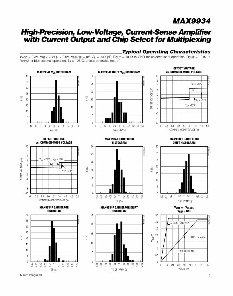
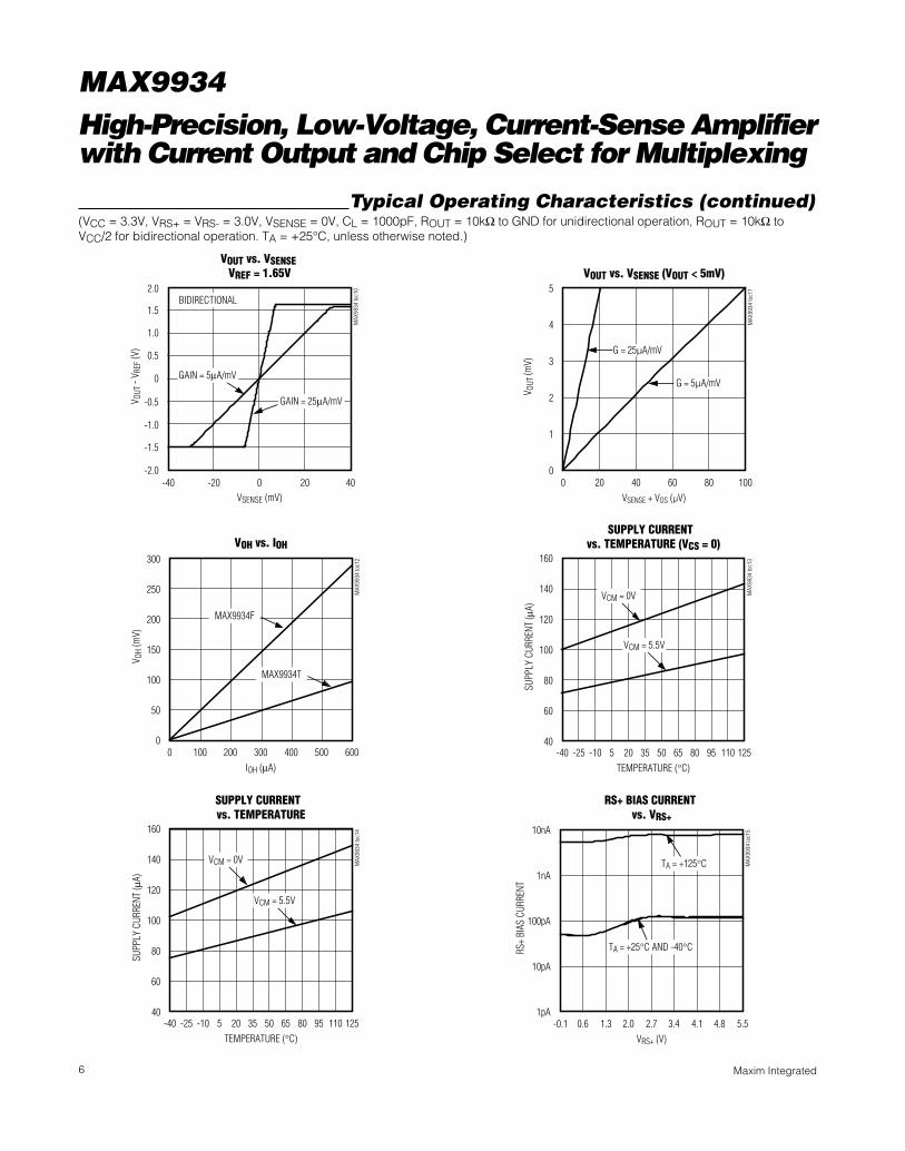
Typical Operating Characteristics(VCC = 3.3V, VRS+ = VRS- = 3.0V, VSENSE = 0V, CL = 1000pF, ROUT = 10kΩ to GND for unidirectional operation, ROUT = 10kΩ toVCC/2 for bidirectional operation. TA = +25°C, unless otherwise noted.)
MAX9934T VOS HISTOGRAM
MAX
9934
toc0
1
VOS (FV)
N (%
)
-8 -6 -4 -2 0 2 4 6 8
5
10
15
20
25
30
35
40
0-10 10
OFFSET VOLTAGEvs. COMMON-MODE VOLTAGE
MAX
9934
toc0
4
COMMON-MODE VOLTAGE (V)
OFFS
ET V
OLTA
GE (F
V)
4.84.12.7 3.41.3 2.00.6
-8
-6
-4
-2
0
2
4
6
8
10
-10-0.1 5.5
VCC = 3.3V
VCC = 3.6V
VCC = 2.5V
MAX9934T DRIFT VOS HISTOGRAM
MAX
9934
toc0
2
TCVOS (nV/NC)
N (%
)
6 12 18 24 30 36 42 48 54
5
10
15
20
25
30
00 60
OFFSET VOLTAGEvs. COMMON-MODE VOLTAGE
MAX
9934
toc0
3
COMMON-MODE VOLTAGE (V)
OFFS
ET V
OLTA
GE (F
V)
4.84.12.7 3.41.3 2.00.6
-8
-6
-4
-2
0
2
4
6
8
10
-10-0.1 5.5
TA = +125NC
TA = +25NC
TA = -40NC
0
0.5
1.5
1.0
2.5
3.0
2.0
3.5
0 20 3010 40 50 60 70 80
VOUT vs. VSENSEVREF = GND
MAX
9934
toc0
9
VSENSE (mV)
V OUT
(V)
GAIN = 25µA/mV
GAIN = 5µA/mV
UNIDIRECTIONAL
5
10
15
20
25
30
0
-0.1
6
-0.1
2
-0.0
8
-0.0
4 0
0.04
0.08
0.12
0.16
-0.2
0
0.20
MAX9934T GAIN ERRORHISTOGRAM
MAX
9934
toc0
5
GE (%)
N (%
)
5
10
15
20
25
30
35
0
-160
-120 -80
-40 0 40 80 120
160
-200 200
MAX9934T GAIN ERRORDRIFT HISTOGRAM
MAX
9934
toc0
6
TC GE (PPM/NC)
N (%
)
5
10
15
20
25
30
35
40
0
-0.1
6
-0.1
2
-0.0
8
-0.0
4 0
0.04
0.08
0.12
0.16
-0.2
0
0.20
MAX9934F GAIN ERRORHISTOGRAM
MAX
9934
toc0
7
GE (%)
N (%
)
-160
-120 -80
-40 0 40 80 120
160
-200 200
MAX9934F GAIN ERROR DRIFTHISTOGRAM
MAX
9934
toc0
8
TC GE (PPM/°C)
N (%
)
5
10
15
20
25
0
MAX9934High-Precision, Low-Voltage, Current-Sense Amplifierwith Current Output and Chip Select for Multiplexing
6 Maxim Integrated
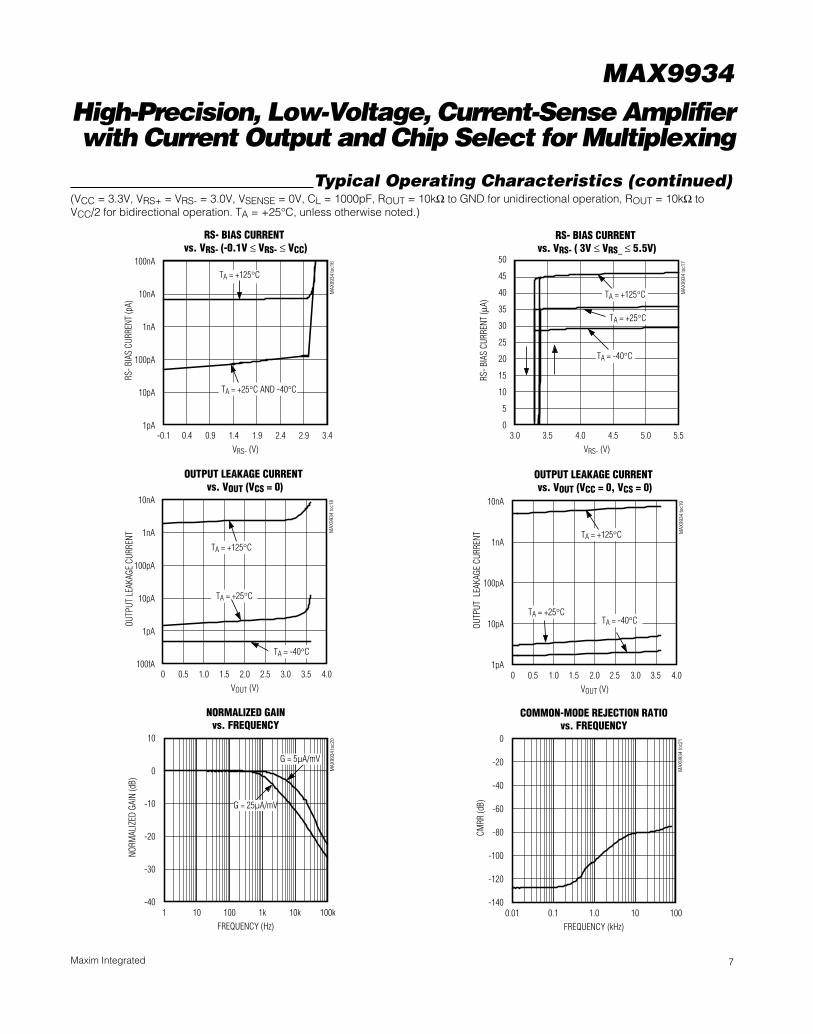
Typical Operating Characteristics (continued)(VCC = 3.3V, VRS+ = VRS- = 3.0V, VSENSE = 0V, CL = 1000pF, ROUT = 10kΩ to GND for unidirectional operation, ROUT = 10kΩ toVCC/2 for bidirectional operation. TA = +25°C, unless otherwise noted.)
-2.0
-0.5
-1.0
-1.5
0.5
0
1.5
1.0
2.0
VOUT vs. VSENSEVREF = 1.65V
MAX
9934
toc1
0
VSENSE (mV)
V OUT
- V R
EF (V
)
-40 -20 0 20 40
GAIN = 25µA/mV
GAIN = 5µA/mV
BIDIRECTIONAL
VOUT vs. VSENSE (VOUT < 5mV)
MAX
9934
toc1
1
VSENSE + VOS (FV)
V OUT
(mV)
80604020
1
2
3
4
5
00 100
G = 25FA/mV
G = 5FA/mV
0
100
50
200
150
250
300
0 200 300100 400 500 600
VOH vs. IOH
MAX
9934
toc1
2
IOH (µA)
V OH
(mV)
MAX9934F
MAX9934T
40
80
60
120
100
140
160
-40 -10 5 20-25 35 50 65 80 95 110 125
SUPPLY CURRENT vs. TEMPERATURE (VCS = 0)
MAX
9934
toc1
3
TEMPERATURE (°C)
SUPP
LY C
URRE
NT (µ
A)
VCM = 0V
VCM = 5.5V
40
80
60
120
100
140
160
-40 -10 5 20-25 35 50 65 80 95 110 125
SUPPLY CURRENT vs. TEMPERATURE
MAX
9934
toc1
4
TEMPERATURE (°C)
SUPP
LY C
URRE
NT (µ
A)
VCM = 0V
VCM = 5.5V
1pA
10pA
100pA
1nA
10nA
-0.1 1.3 2.7 4.10.6 2.0 3.4 4.8 5.5
RS+ BIAS CURRENTvs. VRS+
MAX
9934
toc1
5
VRS+ (V)
RS+
BIAS
CUR
RENT
TA = +125°C
TA = +25°C AND -40°C
MAX9934High-Precision, Low-Voltage, Current-Sense Amplifierwith Current Output and Chip Select for Multiplexing
7Maxim Integrated
Typical Operating Characteristics (continued)(VCC = 3.3V, VRS+ = VRS- = 3.0V, VSENSE = 0V, CL = 1000pF, ROUT = 10kΩ to GND for unidirectional operation, ROUT = 10kΩ toVCC/2 for bidirectional operation. TA = +25°C, unless otherwise noted.)
1pA
10pA
1nA
100pA
10nA
100nA
-0.1 0.90.4 1.4 1.9 2.4 2.9 3.4
RS- BIAS CURRENTvs. VRS- (-0.1V ≤ VRS- ≤ VCC)
MAX
9934
toc1
6
VRS- (V)
RS- B
IAS
CURR
ENT
(pA)
TA = +125°C
TA = +25°C AND -40°C
0
15
10
5
20
25
30
35
40
45
50
3.0 4.03.5 4.5 5.0 5.5
RS- BIAS CURRENTvs. VRS- ( 3V ≤ VRS_ ≤ 5.5V)
MAX
9934
toc1
7
VRS- (V)
RS- B
IAS
CURR
ENT
(µA)
TA = +125°C
TA = +25°C
TA = -40°C
100fA
1pA
100pA
10pA
1nA
10nA
0 1.0 1.50.5 2.0 2.5 3.0 3.5 4.0
OUTPUT LEAKAGE CURRENTvs. VOUT (VCS = 0)
MAX
9934
toc1
8
VOUT (V)
OUTP
UT L
EAKA
GE C
URRE
NT
TA = +125°C
TA = +25°C
TA = -40°C1pA
10pA
100pA
1nA
10nA
0 1.0 2.0 3.00.5 1.5 2.5 3.5 4.0
OUTPUT LEAKAGE CURRENTvs. VOUT (VCC = 0, VCS = 0)
MAX
9934
toc1
9
VOUT (V)
OUTP
UT L
EAKA
GE C
URRE
NT TA = +125°C
TA = +25°CTA = -40°C
NORMALIZED GAINvs. FREQUENCY
MAX
9934
toc2
0
FREQUENCY (Hz)
NORM
ALIZ
ED G
AIN
(dB)
10k1k10010
-30
-20
-10
0
10
-401 100k
G = 5FA/mV
G = 25FA/mV
COMMON-MODE REJECTION RATIOvs. FREQUENCY
MAX
9934
toc2
1
FREQUENCY (kHz)
CMRR
(dB)
101.00.1
-120
-100
-80
-60
-40
-20
0
-1400.01 100
MAX9934High-Precision, Low-Voltage, Current-Sense Amplifierwith Current Output and Chip Select for Multiplexing
8 Maxim Integrated
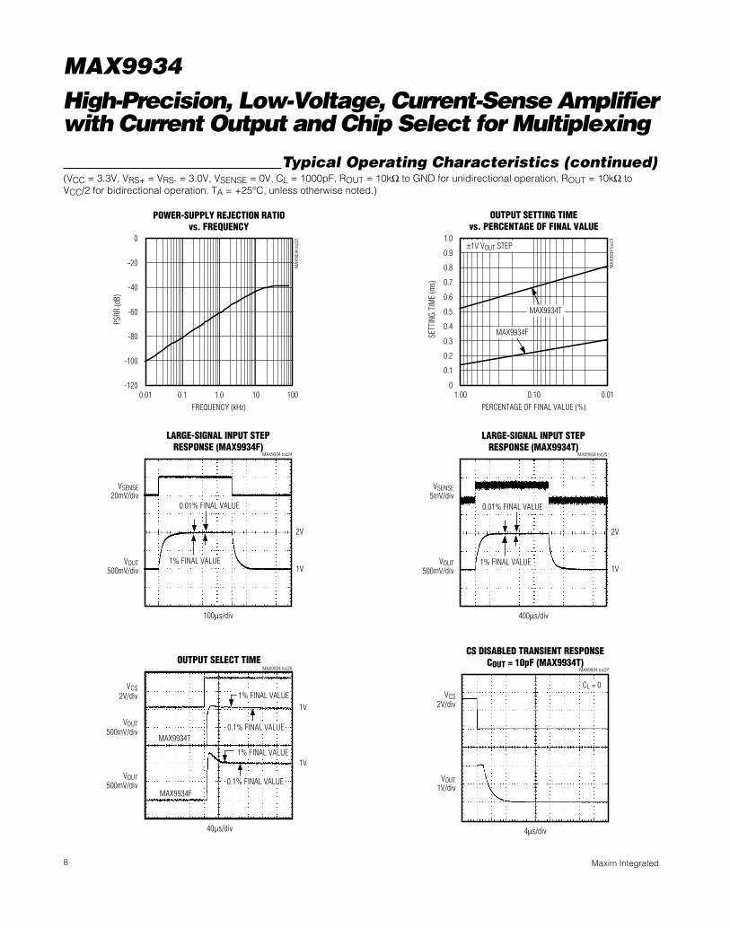
Typical Operating Characteristics (continued)(VCC = 3.3V, VRS+ = VRS- = 3.0V, VSENSE = 0V, CL = 1000pF, ROUT = 10kΩ to GND for unidirectional operation, ROUT = 10kΩ toVCC/2 for bidirectional operation. TA = +25°C, unless otherwise noted.)
POWER-SUPPLY REJECTION RATIOvs. FREQUENCY
MAX
9934
toc2
2
FREQUENCY (kHz)
PSRR
(dB)
101.00.1
-100
-80
-60
-40
-20
0
-1200.01 100
OUTPUT SETTING TIMEvs. PERCENTAGE OF FINAL VALUE
MAX
9934
toc2
3
PERCENTAGE OF FINAL VALUE (%)
SETT
ING
TIM
E (m
s)
0.10
0.1
0.2
0.3
0.4
0.5
0.6
0.7
0.8
0.9
1.0
01.00 0.01
±1V VOUT STEP
MAX9934T
MAX9934F
100µs/div
LARGE-SIGNAL INPUT STEPRESPONSE (MAX9934F)
VSENSE20mV/div
VOUT500mV/div
MAX9934 toc24
0.01% FINAL VALUE
1% FINAL VALUE
2V
1V
400µs/div
LARGE-SIGNAL INPUT STEPRESPONSE (MAX9934T)
VSENSE5mV/div
VOUT500mV/div
MAX9934 toc25
0.01% FINAL VALUE
1% FINAL VALUE
2V
1V
MAX9934 toc26
1V
1V
40Fs/div
VCS2V/div
VOUT500mV/div
VOUT500mV/div
1% FINAL VALUE
0.1% FINAL VALUE
0.1% FINAL VALUEMAX9934T
MAX9934F
1% FINAL VALUE
OUTPUT SELECT TIME
4µs/div
CS DISABLED TRANSIENT RESPONSECOUT = 10pF (MAX9934T)
VCS2V/div
VOUT1V/div
MAX9934 toc27
CL = 0
MAX9934High-Precision, Low-Voltage, Current-Sense Amplifierwith Current Output and Chip Select for Multiplexing
9Maxim Integrated
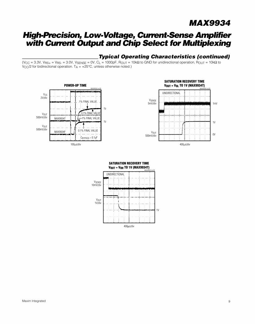
Typical Operating Characteristics (continued)(VCC = 3.3V, VRS+ = VRS- = 3.0V, VSENSE = 0V, CL = 1000pF, ROUT = 10kΩ to GND for unidirectional operation, ROUT = 10kΩ toVCC/2 for bidirectional operation. TA = +25°C, unless otherwise noted.)
POWER-UP TIMEMAX9934 toc28
1V
1V
100Fs/div
VCS2V/div
VOUT500mV/div
VOUT500mV/div
MAX9934T
MAX9934F
1% FINAL VALUE
0.1% FINAL VALUE
CBYPASS = 0.1µF
1% FINAL VALUE
0.1% FINAL VALUE
SATURATION RECOVERY TIMEVOUT = VOL TO 1V (MAX9934T)
MAX9934 toc29
1mV
0V
1V
UNIDIRECTIONAL
400Fs/div
VSENSE5mV/div
VOUT500mV/div
400µs/div
SATURATION RECOVERY TIMEVOUT = VOH TO 1V (MAX9934T)
VSENSE10mV/div
VOUT1V/div
MAX9934 toc30
1V
UNIDIRECTIONAL
MAX9934High-Precision, Low-Voltage, Current-Sense Amplifierwith Current Output and Chip Select for Multiplexing
10 Maxim Integrated
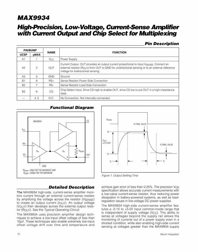
Detailed DescriptionThe MAX9934 high-side, current-sense amplifier moni-tors current through an external current-sense resistorby amplifying the voltage across the resistor (VSENSE)to create an output current (IOUT). An output voltage(VOUT) then develops across the external output resis-tor (ROUT). See the Typical Operating Circuit.The MAX9934 uses precision amplifier design tech-niques to achieve a low-input offset voltage of less than10µV. These techniques also enable extremely low-inputoffset voltage drift over time and temperature and
achieve gain error of less than 0.25%. The precision VOSspecification allows accurate current measurements witha low-value current-sense resistor, thus reducing powerdissipation in battery-powered systems, as well as load-regulation issues in low-voltage DC power supplies.
The MAX9934 high-side current-sense amplifier fea-tures a -0.1V to +5.5V input common-mode range thatis independent of supply voltage (VCC). This ability tosense at voltages beyond the supply rail allows themonitoring of currents out of a power supply even in ashorted condition, while also enabling high-side currentsensing at voltages greater than the MAX9934 supply
Pin DescriptionPIN/BUMP
UCSP µMAXNAME FUNCTION
A1 1 VCC Power Supply
A2 2 OUTCurrent Output. OUT provides an output current proportional to input VSENSE. Connect anexternal resistor (ROUT) from OUT to GND for unidirectional sensing or to an external referencevoltage for bidirectional sensing.
A3 3 GND Ground
B1 8 RS+ Sense Resistor Power Side Connection
B2 7 RS- Sense Resistor Load Side Connection
B3 6 CSChip-Select Input. Drive CS high to enable OUT, drive CS low to put OUT in a high-impedancestate.
— 4, 5 N.C. No Connection. Not internally connected.
% FINAL VALUE
VOUT±1V STEP
tS
2V
1V
tS
% FINAL VALUE
VSENSE
Figure 1. Output Settling Time
CS
OUT
GND
RS-
RS+
VCC
*RGAINGm
MAX9934
Gm
*RGAIN = 40Ω FOR THE MAX9934T AND RGAIN = 200Ω FOR THE MAX9934F.
Functional Diagram
MAX9934High-Precision, Low-Voltage, Current-Sense Amplifierwith Current Output and Chip Select for Multiplexing
11Maxim Integrated
voltage. Further, when VCC = 0, the amplifier maintainsan extremely high impedance on both its inputs andoutput, up to the maximum operating voltages (see theAbsolute Maximum Ratings section).
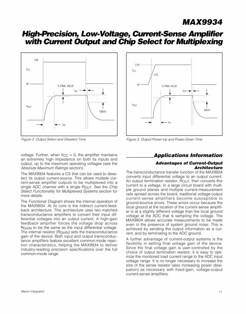
The MAX9934 features a CS that can be used to dese-lect its output current-source. This allows multiple cur-rent-sense amplifier outputs to be multiplexed into asingle ADC channel with a single ROUT. See the ChipSelect Functionality for Multiplexed Systems section formore details.
The Functional Diagram shows the internal operation ofthe MAX9934. At its core is the indirect current-feed-back architecture. This architecture uses two matchedtransconductance amplifiers to convert their input dif-ferential voltages into an output current. A high-gainfeedback amplifier forces the voltage drop acrossRGAIN to be the same as the input differential voltage.The internal resistor (RGAIN) sets the transconductancegain of the device. Both input and output transconduc-tance amplifiers feature excellent common-mode rejec-tion characteristics, helping the MAX9934 to deliverindustry-leading precision specifications over the fullcommon-mode range.
Applications Information Advantages of Current-Output
ArchitectureThe transconductance transfer function of the MAX9934converts input differential voltage to an output current.An output termination resistor, ROUT, then converts thiscurrent to a voltage. In a large circuit board with multi-ple ground planes and multiple current-measurementrails spread across the board, traditional voltage-outputcurrent-sense amplifiers become susceptible toground-bounce errors. These errors occur because thelocal ground at the location of the current-sense amplifi-er is at a slightly different voltage than the local groundvoltage at the ADC that is sampling the voltage. TheMAX9934 allows accurate measurements to be madeeven in the presence of system ground noise. This isachieved by sending the output information as a cur-rent, and by terminating to the ADC ground.
A further advantage of current-output systems is theflexibility in setting final voltage gain of the device.Since the final voltage gain is user-controlled by thechoice of output termination resistor, it is easy to opti-mize the monitored load current range to the ADC inputvoltage range. It is no longer necessary to increase thesize of the sense resistor (also increasing power dissi-pation) as necessary with fixed-gain, voltage-outputcurrent-sense amplifiers.
100mV
tHZ
% FINAL VALUE
tZH
VOUT
0V
1.8V
VCS
Figure 2. Output Select and Deselect Time
100mV
tPD
% FINAL VALUE
tPU
VCC
VOUT
0V
3.3V
2.5V
Figure 3. Output Power-Up and Power-Down Time
MAX9934High-Precision, Low-Voltage, Current-Sense Amplifierwith Current Output and Chip Select for Multiplexing
12 Maxim Integrated
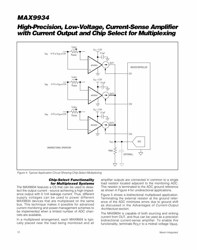
Chip-Select Functionalityfor Multiplexed Systems
The MAX9934 features a CS that can be used to dese-lect the output current - source achieving a high-imped-ance output with 0.1nA leakage current. Thus, differentsupply voltages can be used to power differentMAX9934 devices that are multiplexed on the samebus. This technique makes it possible for advancedcurrent monitoring and power-management schemes tobe implemented when a limited number of ADC chan-nels are available.
In a multiplexed arrangement, each MAX9934 is typi-cally placed near the load being monitored and all
amplifier outputs are connected in common to a singleload resistor located adjacent to the monitoring ADC.This resistor is terminated to the ADC ground referenceas shown in Figure 4 for unidirectional applications.
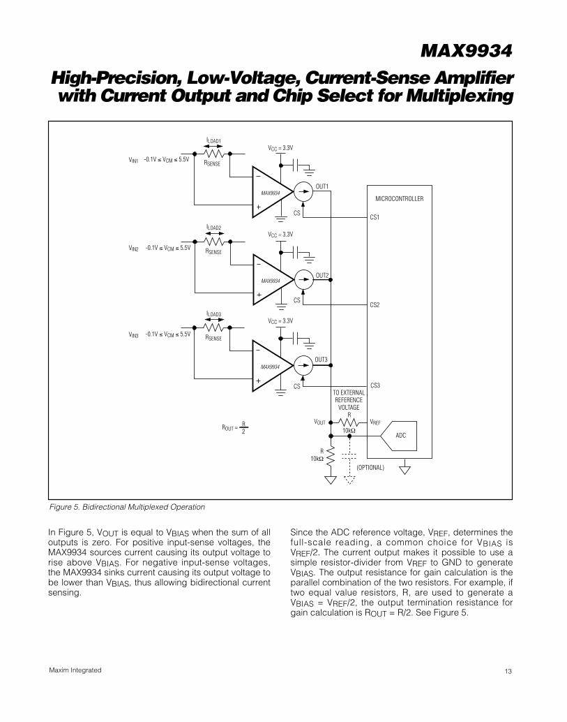
Figure 5 shows a bidirectional multiplexed application.Terminating the external resistor at the ground refer-ence of the ADC minimizes errors due to ground shiftas discussed in the Advantages of Current-OutputArchitecture section.
The MAX9934 is capable of both sourcing and sinkingcurrent from OUT, and thus can be used as a precisionbidirectional current-sense amplifier. To enable thisfunctionality, terminate ROUT to a midrail voltage VBIAS.
VCC = 3.3V
VCC = 3.3V
VCC = 3.3V
RSENSE-0.1V ≤ VCM ≤ 5.5V
RSENSE-0.1V ≤ VCM ≤ 5.5V
RSENSE-0.1V ≤ VCM ≤ 5.5V
MAX9934
MAX9934
MAX9934
10kΩ
(OPTIONAL)
ADC
CS3
CS2
CS1
MICROCONTROLLER
VIN1
VIN2
VIN3
ILOAD3
ILOAD2
ILOAD1
VOUT
0.1µF
0.1µF
0.1µF
OUT3
OUT2
OUT1
UNIDIRECTIONAL OPERATION
Figure 4. Typical Application Circuit Showing Chip-Select Multiplexing
MAX9934High-Precision, Low-Voltage, Current-Sense Amplifierwith Current Output and Chip Select for Multiplexing
13Maxim Integrated
In Figure 5, VOUT is equal to VBIAS when the sum of alloutputs is zero. For positive input-sense voltages, theMAX9934 sources current causing its output voltage torise above VBIAS. For negative input-sense voltages,the MAX9934 sinks current causing its output voltage tobe lower than VBIAS, thus allowing bidirectional currentsensing.
Since the ADC reference voltage, VREF, determines thefull-scale reading, a common choice for VBIAS isVREF/2. The current output makes it possible to use asimple resistor-divider from VREF to GND to generateVBIAS. The output resistance for gain calculation is theparallel combination of the two resistors. For example, iftwo equal value resistors, R, are used to generate aVBIAS = VREF/2, the output termination resistance forgain calculation is ROUT = R/2. See Figure 5.
VCC = 3.3V
VCC = 3.3V
VCC = 3.3V
RSENSE-0.1V ≤ VCM ≤ 5.5V
RSENSE-0.1V ≤ VCM ≤ 5.5V
RSENSE-0.1V ≤ VCM ≤ 5.5V
MAX9934
MAX9934
MAX9934
R10kΩ
ADC
VREF
CS2
CS1
MICROCONTROLLER
CS
CS
CS
TO EXTERNALREFERENCE
VOLTAGE
10kΩ
R
CS3
(OPTIONAL)
VIN1
VIN2
VIN3
ILOAD3
ILOAD2
ILOAD1
VOUT
OUT3
OUT2
OUT1
ROUT = R2
Figure 5. Bidirectional Multiplexed Operation
MAX9934High-Precision, Low-Voltage, Current-Sense Amplifierwith Current Output and Chip Select for Multiplexing
14 Maxim Integrated
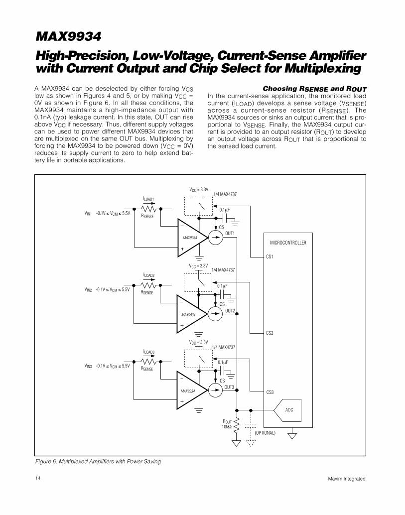
A MAX9934 can be deselected by either forcing VCSlow as shown in Figures 4 and 5, or by making VCC =0V as shown in Figure 6. In all these conditions, theMAX9934 maintains a high-impedance output with0.1nA (typ) leakage current. In this state, OUT can riseabove VCC if necessary. Thus, different supply voltagescan be used to power different MAX9934 devices thatare multiplexed on the same OUT bus. Multiplexing byforcing the MAX9934 to be powered down (VCC = 0V)reduces its supply current to zero to help extend bat-tery life in portable applications.
Choosing RSENSE and ROUTIn the current-sense application, the monitored loadcurrent (ILOAD) develops a sense voltage (VSENSE)across a current-sense resistor (RSENSE). TheMAX9934 sources or sinks an output current that is pro-portional to VSENSE. Finally, the MAX9934 output cur-rent is provided to an output resistor (ROUT) to developan output voltage across ROUT that is proportional tothe sensed load current.
VCC = 3.3V
RSENSE-0.1V ≤ VCM ≤ 5.5V
MAX9934
ROUT10kΩ
(OPTIONAL)
ADC
CS2
CS1
MICROCONTROLLER
CS
CS3
VCC = 3.3V
RSENSE-0.1V ≤ VCM ≤ 5.5V
MAX9934
CS
VCC = 3.3V
RSENSE-0.1V ≤ VCM ≤ 5.5V
MAX9934
CS
1/4 MAX4737
1/4 MAX4737
1/4 MAX4737
VIN1
VIN2
VIN3
ILOAD1
OUT3
OUT2
OUT1
0.1µF
0.1µF
0.1µF
ILOAD3
ILOAD2
Figure 6. Multiplexed Amplifiers with Power Saving
MAX9934High-Precision, Low-Voltage, Current-Sense Amplifierwith Current Output and Chip Select for Multiplexing
15Maxim Integrated
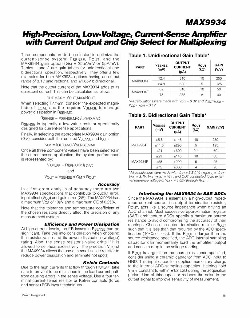
Three components are to be selected to optimize thecurrent-sense system: RSENSE, ROUT, and theMAX9934 gain option (GM = 25µA/mV or 5µA/mV).Tables 1 and 2 are gain tables for unidirectional andbidirectional operation, respectively. They offer a fewexamples for both MAX9934 options having an outputrange of 3.1V unidirectional and ±1.65V bidirectional.
Note that the output current of the MAX9934 adds to itsquiescent current. This can be calculated as follows:
IOUT,MAX = VOUT,MAX/ROUT
When selecting RSENSE, consider the expected magni-tude of ILOAD and the required VSENSE to managepower dissipation in RSENSE:
RSENSE = VSENSE,MAX/ILOAD,MAX
RSENSE is typically a low-value resistor specificallydesigned for current-sense applications.
Finally, in selecting the appropriate MAX9934 gain option(GM), consider both the required VSENSE and IOUT:
GM = IOUT,MAX/VSENSE,MAX
Once all three component values have been selected inthe current-sense application, the system performanceis represented by:
VSENSE = RSENSE x ILOAD
and
VOUT = VSENSE x GM x ROUT
AccuracyIn a first-order analysis of accuracy there are twoMAX9934 specifications that contribute to output error,input offset (VOS) and gain error (GE). The MAX9934 hasa maximum VOS of 10µV and a maximum GE of 0.25%.
Note that the tolerance and temperature coefficient ofthe chosen resistors directly affect the precision of anymeasurement system.
Efficiency and Power DissipationAt high-current levels, the I2R losses in RSENSE can besignificant. Take this into consideration when choosingthe resistor value and its power dissipation (wattage)rating. Also, the sense resistor’s value drifts if it isallowed to self-heat excessively. The precision VOS ofthe MAX9934 allows the use of a small sense resistor toreduce power dissipation and eliminate hot spots.
Kelvin ContactsDue to the high currents that flow through RSENSE, takecare to prevent trace resistance in the load current pathfrom causing errors in the sense voltage. Use a four ter-minal current-sense resistor or Kelvin contacts (forceand sense) PCB layout techniques.
Interfacing the MAX9934 to SAR ADCsSince the MAX9934 is essentially a high-output imped-ance current-source, its output termination resistor,ROUT, acts like a source impedance when driving anADC channel. Most successive approximation register(SAR) architecture ADCs specify a maximum sourceresistance to avoid compromising the accuracy of theirreadings. Choose the output termination resistor ROUTsuch that it is less than that required by the ADC speci-fication (10kΩ or less). If the ROUT is larger than thesource resistance specified, the ADC internal samplingcapacitor can momentarily load the amplifier outputand cause a drop in the voltage reading.
If ROUT is larger than the source resistance specified,consider using a ceramic capacitor from ADC input toGND. This input capacitor supplies momentary chargeto the internal ADC sampling capacitor, helping holdVOUT constant to within ±1/2 LSB during the acquisitionperiod. Use of this capacitor reduces the noise in theoutput signal to improve sensitivity of measurement.
PARTVSENSE
(mV)
OUTPUTCURRENT
(µA)
ROUT(kΩ)
GAIN(V/V)
12.4 310 10 250MAX9934T
24.8 620 5 125
62 310 10 50MAX9934F
75 375 8 40
Table 1. Unidirectional Gain Table*
*All calculations were made with VCC = 3.3V and VOUT(MAX) =VCC - VOH = 3.1V.
PARTVSENSE
(mV)
OUTPUTCURRENT
(µA)
ROUT(kΩ)
GAIN (V/V)
±5.8 ±145 10 250
±11.6 ±290 5 125MAX9934T
±24 ±600 2.4 60
±29 ±145 10 50
±58 ±290 5 25MAX9934F
±72 ±360 4 20
Table 2. Bidirectional Gain Table*
*All calculations were made with VCC = 3.3V, VOUT(MAX) = VCC -VOH = 3.1V, VOUT(MIN) = VOL, and OUT connected to an exter-nal reference voltage of VREF = 1.65V through ROUT.
MAX9934High-Precision, Low-Voltage, Current-Sense Amplifierwith Current Output and Chip Select for Multiplexing
16 Maxim Integrated
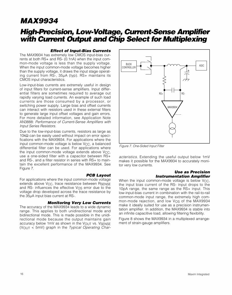
Effect of Input-Bias CurrentsThe MAX9934 has extremely low CMOS input-bias cur-rents at both RS+ and RS- (0.1nA) when the input com-mon-mode voltage is less than the supply voltage.When the input common-mode voltage becomes higherthan the supply voltage, it draws the input stage operat-ing current from RS-, 35µA (typ). RS+ maintains itsCMOS input characteristics.
Low-input-bias currents are extremely useful in designof input filters for current-sense amplifiers. Input differ-ential filters are sometimes required to average outrapidly varying load currents. An example of such loadcurrents are those consumed by a processor, orswitching power supply. Large bias and offset currentscan interact with resistors used in these external filtersto generate large input offset voltages and gain errors.For more detailed information, see Application NoteAN3888: Performance of Current-Sense Amplifiers withInput Series Resistors.
Due to the low-input-bias currents, resistors as large as10kΩ can be easily used without impact on error speci-fications with the MAX9934. For applications where theinput common-mode voltage is below VCC, a balanceddifferential filter can be used. For applications wherethe input common-mode voltage extends above VCC,use a one-sided filter with a capacitor between RS+and RS-, and a filter resistor in series with RS+ to main-tain the excellent performance of the MAX9934. SeeFigure 7.
PCB LayoutFor applications where the input common-mode voltageextends above VCC, trace resistance between RSENSEand RS- influences the effective VOS error due to thevoltage drop developed across the trace resistance bythe 35µA input bias current at RS-.
Monitoring Very Low CurrentsThe accuracy of the MAX9934 leads to a wide dynamicrange. This applies to both unidirectional mode andbidirectional mode. This is made possible in the unidi-rectional mode because the output maintains gainaccuracy below 1mV as shown in the VOUT vs. VSENSE(VOUT < 5mV) graph in the Typical Operating Char-
acteristics. Extending the useful output below 1mVmakes it possible for the MAX9934 to accurately moni-tor very low currents.
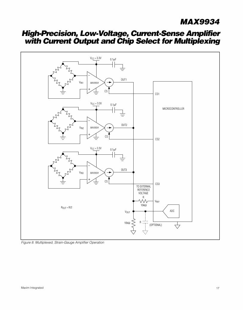
Use as PrecisionInstrumentation Amplifier
When the input common-mode voltage is below VCC,the input bias current of the RS- input drops to the10pA range, the same range as the RS+ input. Thislow-input-bias current in combination with the rail-to-railcommon-mode input range, the extremely high com-mon-mode rejection, and low VOS of the MAX9934make it ideally suited for use as a precision instrumen-tation amplifier. In addition, the MAX9934 is stable intoan infinite capacitive load, allowing filtering flexibility.
Figure 8 shows the MAX9934 in a multiplexed arrange-ment of strain-gauge amplifiers.
BUCKCONTROLLER
RS+ RS-
MAX9934
ASIC
Figure 7. One-Sided Input Filter
MAX9934High-Precision, Low-Voltage, Current-Sense Amplifierwith Current Output and Chip Select for Multiplexing
17Maxim Integrated
CS3
CS1
CS2
MICROCONTROLLER
TO EXTERNALREFERENCEVOLTAGE
VREF
CS
R
R
OUT1
VOUT
VCC = 3.3V 0.1µF
VIN1 MAX9934
CS
OUT2
VCC = 3.3V 0.1µF
VIN2
CS
OUT3
VCC = 3.3V 0.1µF
VIN3
MAX9934
MAX9934
ROUT = R/2
10kΩ(OPTIONAL)
10kΩ
ADC
Figure 8. Multiplexed, Strain-Gauge Amplifier Operation
MAX9934High-Precision, Low-Voltage, Current-Sense Amplifierwith Current Output and Chip Select for Multiplexing
18 Maxim Integrated
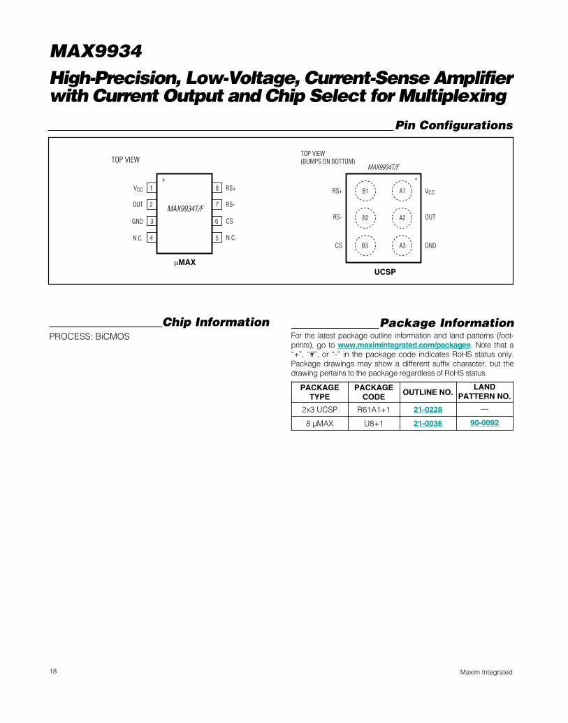
Chip InformationPROCESS: BiCMOS
RS+
RS-
CS
TOP VIEW(BUMPS ON BOTTOM)
B2 A2
B3 A3
B1 A1 VCC
OUT
GND
+
UCSP
MAX9934T/F
CS
N.C.N.C.
1
2
8
7
RS+
RS-OUT
GND
VCC
µMAX
TOP VIEW
3
4
6
5
MAX9934T/F
+
Pin Configurations
Package InformationFor the latest package outline information and land patterns (foot-prints), go to www.maximintegrated.com/packages. Note that a“+”, “#”, or “-” in the package code indicates RoHS status only.Package drawings may show a different suffix character, but thedrawing pertains to the package regardless of RoHS status.
PACKAGETYPE
PACKAGECODE
OUTLINE NO.LAND
PATTERN NO.
2x3 UCSP R61A1+1 21-0228 —
8 µMAX U8+1 21-0036 90-0092
Maxim Integrated cannot assume responsibility for use of any circuitry other than circuitry entirely embodied in a Maxim Integrated product. No circuit patentlicenses are implied. Maxim Integrated reserves the right to change the circuitry and specifications without notice at any time. The parametric values (min andmax limits) shown in the Electrical Characteristics table are guaranteed. Other parametric values quoted in this data sheet are provided for guidance.
Maxim Integrated 160 Rio Robles, San Jose, CA 95134 USA 1-408-601-1000 ________________________________ 19
© 2012 Maxim Integrated Products, Inc. Maxim Integrated and the Maxim Integrated logo are trademarks of Maxim Integrated Products, Inc.
MAX9934High-Precision, Low-Voltage, Current-Sense Amplifierwith Current Output and Chip Select for Multiplexing
Revision History
REVISIONNUMBER
REVISIONDATE
DESCRIPTIONPAGES
CHANGED
0 10/09 Initial release —
1 1/10 Removed µDFN package option 1–10, 18
2 4/10 Removed future product references and updated lead temperature 1, 2
3 11/12 Added automotive packages to Ordering Information 1