MAX2021 High-Dynamic-Range, Direct Up-/Downconversion … · MAX2021 High-Dynamic-Range, Direct...
20
MAX2021 High-Dynamic-Range, Direct Up-/Downconversion 650MHz to 1200MHz Quadrature Mod/Demod EVALUATION KIT AVAILABLE 19-3918; Rev 2; 4/13 For pricing, delivery, and ordering information, please contact Maxim Direct at 1-888-629-4642, or visit Maxim Integrated’s website at www.maximintegrated.com. General Description The MAX2021 low-noise, high-linearity, direct upcon- version/downconversion quadrature modulator/demod- ulator is designed for RFID handheld and portal readers, as well as single and multicarrier 650MHz to 1200MHz GSM/EDGE, cdma2000 ® , WCDMA, and iDEN ® base-station applications. Direct conversion architectures are advantageous since they significantly reduce transmitter or receiver cost, part count, and power consumption as compared to traditional IF-based double conversion systems. In addition to offering excellent linearity and noise perfor- mance, the MAX2021 also yields a high level of compo- nent integration. This device includes two matched passive mixers for modulating or demodulating in-phase and quadrature signals, two LO mixer amplifier drivers, and an LO quadrature splitter. On-chip baluns are also integrated to allow for single-ended RF and LO connec- tions. As an added feature, the baseband inputs have been matched to allow for direct interfacing to the trans- mit DAC, thereby eliminating the need for costly I/Q buffer amplifiers. The MAX2021 operates from a single +5V supply. It is available in a compact 36-pin TQFN package (6mm x 6mm) with an exposed pad. Electrical performance is guaranteed over the extended -40°C to +85°C temper- ature range. Applications RFID Handheld and Portal Readers Single and Multicarrier WCDMA 850 Base Stations Single and Multicarrier cdmaOne™ and cdma2000 Base Stations GSM 850/GSM 900 EDGE Base Stations Predistortion Transmitters and Receivers WiMAX Transmitters and Receivers Fixed Broadband Wireless Access Military Systems Microwave Links Digital and Spread-Spectrum Communication Systems Video-on-Demand (VOD) and DOCSIS Compliant Edge QAM Modulation Cable Modem Termination Systems (CMTS) Features ♦ 650MHz to 1200MHz RF Frequency Range ♦ Scalable Power: External Current-Setting Resistors Provide Option for Operating Device in Reduced-Power/Reduced-Performance Mode ♦ 36-Pin, 6mm x 6mm TQFN Provides High Isolation in a Small Package Modulator Operation: ♦ Meets 4-Carrier WCDMA 65dBc ACLR ♦ +21dBm Typical OIP3 ♦ +58dBm Typical OIP2 ♦ +16.7dBm Typical OP 1dB ♦ -32dBm Typical LO Leakage ♦ 43.5dBc Typical Sideband Suppression ♦ -174dBm/Hz Output Noise Density ♦ DC to 550MHz Baseband Input Allows a Direct Launch DAC Interface, Eliminating the Need for Costly I/Q Buffer Amplifiers ♦ DC-Coupled Input Allows Ability for Customer Offset Voltage Control Demodulator Operation: ♦ +35.2dBm Typical IIP3 ♦ +76dBm Typical IIP2 ♦ > 30dBm IP 1dB ♦ 9.2dB Typical Conversion Loss ♦ 9.3dB Typical NF ♦ 0.06dB Typical I/Q Gain Imbalance ♦ 0.15° I/Q Typical Phase Imbalance Ordering Information PART TEMP RANGE PIN-PACKAGE MAX2021ETX+ -40°C to +85°C 36 TQFN-EP* (6mm x 6mm) MAX2021ETX+T -40°C to +85°C 36 TQFN-EP* (6mm x 6mm) +Denotes a lead(Pb)-free/RoHS-compliant package. *EP = Exposed pad. T = Tape and reel. cdma2000 is a registered certification mark and registered service mark of the Telecommunications Industry Association. iDEN is a registered trademark of Motorola Trademark Holdings, LLC. cdmaOne is a trademark of CDMA Development Group.
Transcript of MAX2021 High-Dynamic-Range, Direct Up-/Downconversion … · MAX2021 High-Dynamic-Range, Direct...

MAX2021
High-Dynamic-Range, Direct Up-/Downconversion 650MHz to 1200MHz Quadrature Mod/Demod
EVALUATION KIT AVAILABLE
19-3918; Rev 2; 4/13
For pricing, delivery, and ordering information, please contact Maxim Direct at 1-888-629-4642, or visit Maxim Integrated’s website at www.maximintegrated.com.
General DescriptionThe MAX2021 low-noise, high-linearity, direct upcon-version/downconversion quadrature modulator/demod-ulator is designed for RFID handheld and portalreaders, as well as single and multicarrier 650MHz to1200MHz GSM/EDGE, cdma2000®, WCDMA, andiDEN® base-station applications. Direct conversionarchitectures are advantageous since they significantlyreduce transmitter or receiver cost, part count, andpower consumption as compared to traditional IF-baseddouble conversion systems.
In addition to offering excellent linearity and noise perfor-mance, the MAX2021 also yields a high level of compo-nent integration. This device includes two matchedpassive mixers for modulating or demodulating in-phaseand quadrature signals, two LO mixer amplifier drivers,and an LO quadrature splitter. On-chip baluns are alsointegrated to allow for single-ended RF and LO connec-tions. As an added feature, the baseband inputs havebeen matched to allow for direct interfacing to the trans-mit DAC, thereby eliminating the need for costly I/Qbuffer amplifiers.
The MAX2021 operates from a single +5V supply. It isavailable in a compact 36-pin TQFN package (6mm x6mm) with an exposed pad. Electrical performance isguaranteed over the extended -40°C to +85°C temper-ature range.
ApplicationsRFID Handheld and Portal Readers
Single and Multicarrier WCDMA 850 Base Stations
Single and Multicarrier cdmaOne™ and cdma2000Base Stations
GSM 850/GSM 900 EDGE Base Stations
Predistortion Transmitters and Receivers
WiMAX Transmitters and Receivers
Fixed Broadband Wireless Access
Military Systems
Microwave Links
Digital and Spread-Spectrum Communication Systems
Video-on-Demand (VOD) and DOCSIS CompliantEdge QAM Modulation
Cable Modem Termination Systems (CMTS)
Features♦ 650MHz to 1200MHz RF Frequency Range
♦ Scalable Power: External Current-SettingResistors Provide Option for Operating Device inReduced-Power/Reduced-Performance Mode
♦ 36-Pin, 6mm x 6mm TQFN Provides High Isolationin a Small Package
Modulator Operation:
♦ Meets 4-Carrier WCDMA 65dBc ACLR
♦ +21dBm Typical OIP3
♦ +58dBm Typical OIP2
♦ +16.7dBm Typical OP1dB
♦ -32dBm Typical LO Leakage
♦ 43.5dBc Typical Sideband Suppression
♦ -174dBm/Hz Output Noise Density
♦ DC to 550MHz Baseband Input Allows a DirectLaunch DAC Interface, Eliminating the Need forCostly I/Q Buffer Amplifiers
♦ DC-Coupled Input Allows Ability for CustomerOffset Voltage Control
Demodulator Operation:
♦ +35.2dBm Typical IIP3
♦ +76dBm Typical IIP2
♦ > 30dBm IP1dB
♦ 9.2dB Typical Conversion Loss
♦ 9.3dB Typical NF
♦ 0.06dB Typical I/Q Gain Imbalance
♦ 0.15° I/Q Typical Phase Imbalance
Ordering Information
PART TEMP RANGE PIN-PACKAGE
MAX2021ETX+ -40°C to +85°C 36 TQFN-EP* (6mm x 6mm)
MAX2021ETX+T -40°C to +85°C 36 TQFN-EP* (6mm x 6mm)
+Denotes a lead(Pb)-free/RoHS-compliant package.*EP = Exposed pad.T = Tape and reel.
cdma2000 is a registered certification mark and registered service mark of the Telecommunications Industry Association.
iDEN is a registered trademark of Motorola Trademark Holdings, LLC.
cdmaOne is a trademark of CDMA Development Group.
MAX2021High-Dynamic-Range, Direct Up-/Downconversion 650MHz to 1200MHz Quadrature Mod/Demod
2 Maxim Integrated
ABSOLUTE MAXIMUM RATINGS
Stresses beyond those listed under “Absolute Maximum Ratings” may cause permanent damage to the device. These are stress ratings only, and functionaloperation of the device at these or any other conditions beyond those indicated in the operational sections of the specifications is not implied. Exposure toabsolute maximum rating conditions for extended periods may affect device reliability.
VCC_ to GND ........................................................-0.3V to +5.5VBBI+, BBI-, BBQ+, BBQ- to GND...............-3.5V to (VCC + 0.3V)LO, RF to GND Maximum Current ......................................30mARF Input Power ...............................................................+30dBmBaseband Differential I/Q Input Power...........................+20dBm LO Input Power...............................................................+10dBmRBIASLO1 Maximum Current .............................................10mARBIASLO2 Maximum Current .............................................10mA
RBIASLO3 Maximum Current .............................................10mAContinuous Power Dissipation (Note 1) ...............................7.6WOperating Case Temperature Range (Note 2) ....-40°C to +85°CMaximum Junction Temperature .....................................+150°CStorage Temperature Range .............................-65°C to +150°CLead Temperature (soldering, 10s) .................................+300°C Soldering Temperature (reflow) .......................................+260°C
DC ELECTRICAL CHARACTERISTICS(MAX2021 Typical Application Circuit, VCC = 4.75V to 5.25V, GND = 0V, I/Q inputs terminated into 50Ω to GND, LO input terminated into50Ω, RF output terminated into 50Ω, 0V common-mode input, R1 = 432Ω, R2 = 619Ω, R3 = 332Ω, TC = -40°C to +85°C, unless otherwisenoted. Typical values are at VCC = 5V, TC = +25°C, unless otherwise noted.)
PARAMETER SYMBOL CONDITIONS MIN TYP MAX UNITS
Supply Voltage VCC 4.75 5.00 5.25 V
Total Supply Current ITOTAL Pins 3, 13, 15, 31, 33 all connected to VCC 230 271 315 mA
Total Power Dissipation 1355 1654 mW
RECOMMENDED AC OPERATING CONDITIONSPARAMETER SYMBOL CONDITIONS MIN TYP MAX UNIT
RF Frequency (Note 5) fRF 650 1200 MHz
LO Frequency (Note 5) fLO 750 1200 MHz
IF Frequency (Note 5) fIF 550 MHz
LO Power Range PLO -6 +3 dBm
Note 1: Based on junction temperature TJ = TC + (θJC x VCC x ICC). This formula can be used when the temperature of theexposed pad is known while the device is soldered down to a PCB. See the Applications Information section for details.The junction temperature must not exceed +150°C.
Note 2: TC is the temperature on the exposed pad of the package. TA is the ambient temperature of the device and PCB.
Note 3: Junction temperature TJ = TA + (θJA x VCC x ICC). This formula can be used when the ambient temperature of the PCB isknown. The junction temperature must not exceed +150°C.
Note 4: Package thermal resistances were obtained using the method described in JEDEC specification JESD51-7, using a four-layerboard. For detailed information on package thermal considerations, refer to www.maximintegrated.com/thermal-tutorial.
PACKAGE THERMAL CHARACTERISTICSTQFN
Junction-to-AmbientThermal Resistance (θJA) (Notes 3, 4) .......................+34°C/W
Junction-to-CaseThermal Resistance (θJC) (Notes 1, 4) ......................+8.5°C/W
MAX2021High-Dynamic-Range, Direct Up-/Downconversion
650MHz to 1200MHz Quadrature Mod/Demod
3Maxim Integrated
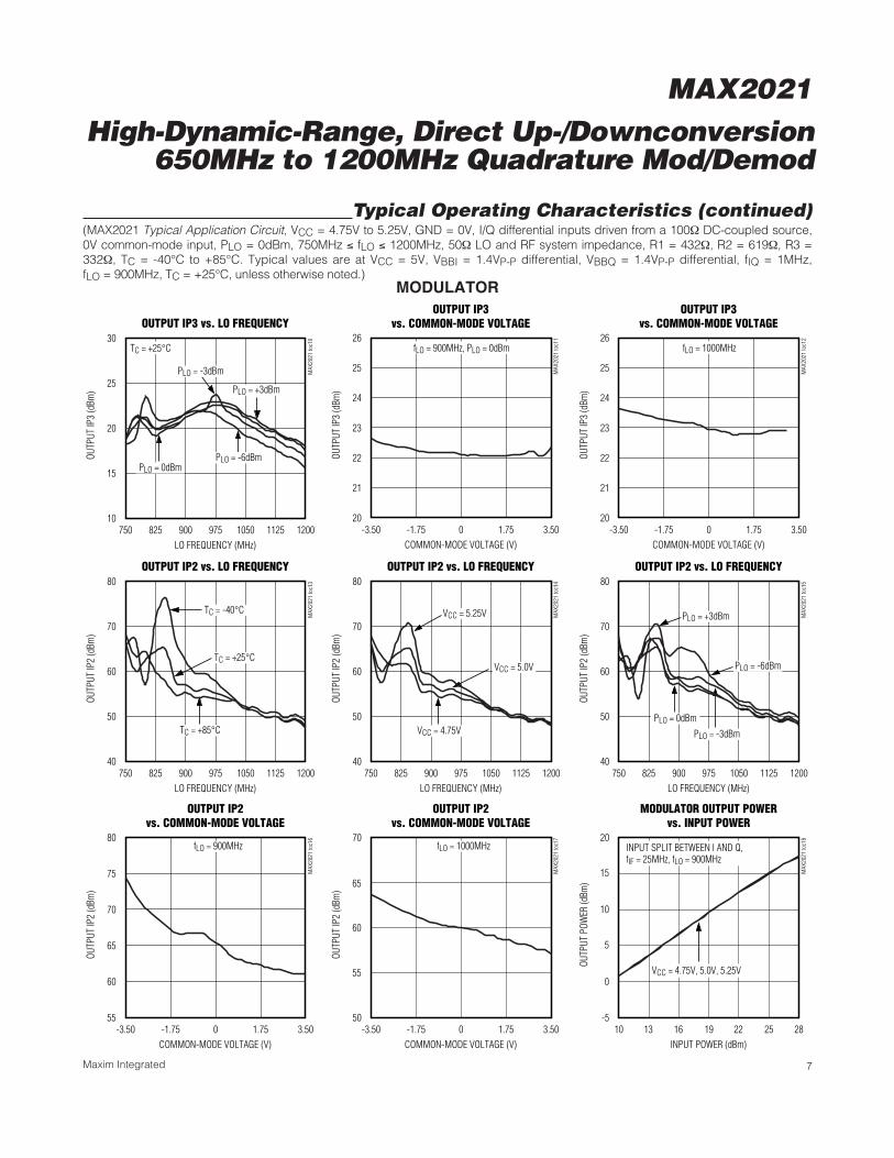
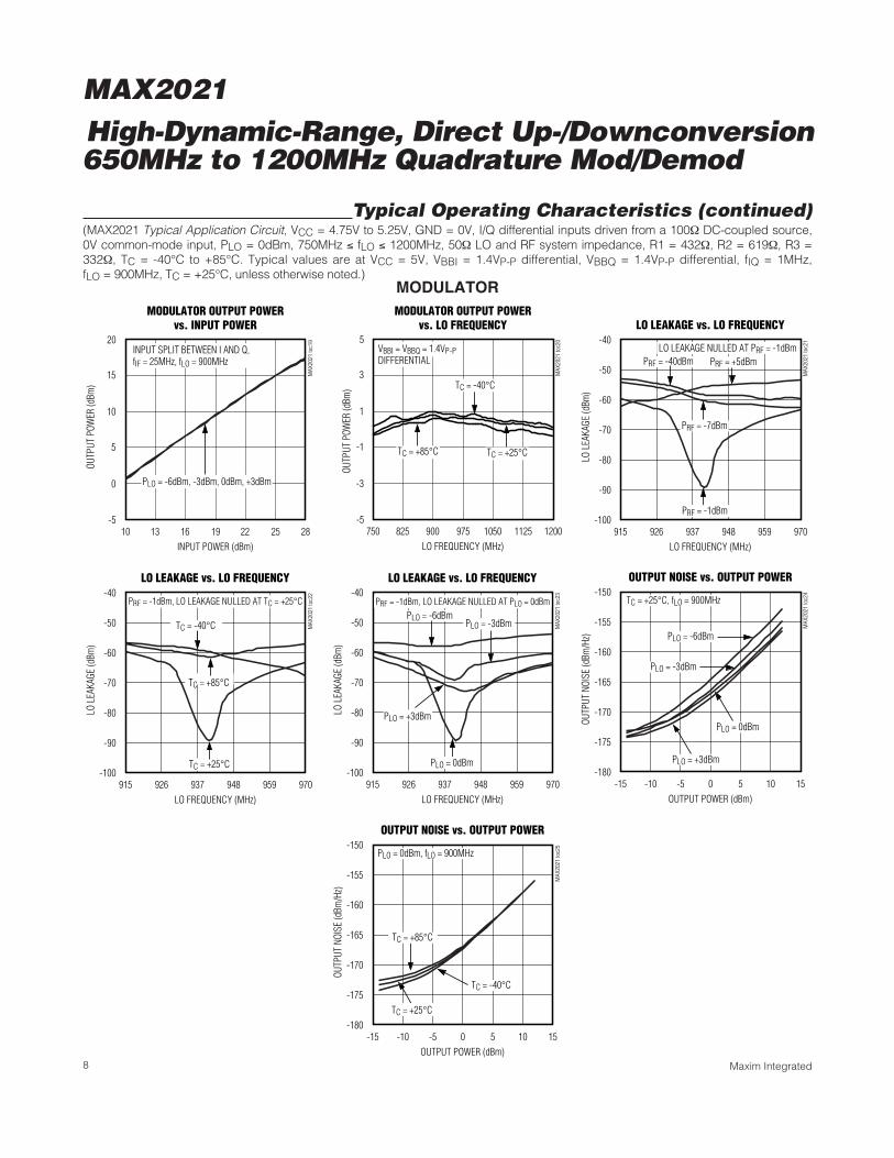
AC ELECTRICAL CHARACTERISTICS (Modulator)(MAX2021 Typical Application Circuit, VCC = 4.75V to 5.25V, GND = 0V, I/Q differential inputs driven from a 100Ω DC-coupled source,0V common-mode input, PLO = 0dBm, 750MHz ≤ fLO ≤ 1200MHz, 50Ω LO and RF system impedance, R1 = 432Ω, R2 = 619Ω, R3 =332Ω, TC = -40°C to +85°C. Typical values are at VCC = 5V, VBBI = 1.4VP-P differential, VBBQ = 1.4VP-P differential, fIQ = 1MHz, fLO =900MHz, TC = +25°C, unless otherwise noted.) (Note 6)
PARAMETER SYMBOL CONDITIONS MIN TYP MAX UNITS
BASEBAND INPUT
Baseband Input Differential Impedance fIQ = 1MHz 53 Ā
BB Common-Mode Input Voltage Range
-3.5 0 +3.5 V
LO INPUT
LO Input Return Loss RF and IF terminated (Note 7) 12 dB
I/Q MIXER OUTPUTS
fLO = 900MHz 21.1 Output IP3 OIP3
fBB1 = 1.8MHz, fBB2 = 1.9MHz fLO = 1000MHz 22.3
dBm
Output IP2 OIP2 fBB1 = 1.8MHz, fBB2 = 1.9MHz 57.9 dBm
Output P1dB fBB = 25MHz, PLO = 0dBm 16.7 dBm
Output Power POUT 0.7 dBm
Output Power Variation Over Temperature
TC = -40°C to +85°C -0.016 dB/°C
Output-Power Flatness Sweep fBB, PRF flatness for fBB from 1MHz to 50MHz
0.15 dB
ACLR (1st Adjacent Channel 5MHz Offset)
Single-carrier WCDMA (Note 8) 65 dBc
LO Leakage No external calibration, with each baseband input terminated in 50Ā -32 dBm
PLO = 0dBm 30 39.6 Sideband Suppression
No external calibration, fLO = 920MHz PLO = -3dBm 43.5
dBc
Output Noise Density Each baseband input terminated in 50Ā(Note 9)
-174 dBm/Hz
Output Noise Floor POUT = 0dBm, fLO = 900MHz (Note 10) -168 dBm/Hz
RF Return Loss (Note 7) 15 dB

MAX2021High-Dynamic-Range, Direct Up-/Downconversion 650MHz to 1200MHz Quadrature Mod/Demod
4 Maxim Integrated
PARAMETER SYMBOL CONDITIONS MIN TYP MAX UNITS
RF INPUT
Conversion Loss LC fBB = 25MHz (Note 11) 9.2 dB
Noise Figure NF fLO = 900MHz 9.3 dB
Noise Figure Under-Blocking NFBLOCKfBLOCKER = 900MHz, PRF = 11dBm,fRF = fLO = 890MHz (Note 12)
17.8 dB
Input Third-Order Intercept IIP3fRF1 = 925MHz, fRF2 = 926MHz, fLO =900MHz, PRF = PLO = 0dBm, fSPUR = 24MHz
35.2 dBm
Input Second-Order Intercept IIP2fRF1 = 925MHz, fRF2 = 926MHz, fLO =900MHz, PRF = PLO = 0dBm, fSPUR = 51MHz
76 dBm
Input 1dB Compression P1dB fIF = 50MHz, fLO = 900MHz, PLO = 0dBm 30 dBm
I/Q Gain Mismatch fBB = 1MHz, fLO = 900MHz, PLO = 0dBm 0.06 dB
PLO = 0dBm 1.1I/Q Phase Mismatch
fBB = 1MHz,fLO = 900MHz PLO = -3dBm 0.15
Degrees
Minimum Demodulation 3dBBandwidth
LO = 1160MHz LO > RF > 550 MHz
Minimum 1dB Gain Flatness LO = 1160MHz LO > RF > 450 MHz
PARAMETER SYMBOL CONDITIONS MIN TYP MAX UNITS
Conversion Loss Lc 10.1 dB
Noise Figure NFSSB 10.4 dB
Noise Figure Under Blocking NFBLOCKfBLOCKER = 700MHz, PBLOCKER = 11dBm,fLO = 965MHz, fRF = 865MHz, (Note 12)
19 dB
fRF1 = 780MHz, fRF2 = 781MHz,PRF1 = PRF2 = 0dBm, fIF1 = 185MHz,fIF2 = 184MHz
34.5
Input Third-Order InterceptPoint
IIP3fRF1 = 780MHz, fRF2 = 735MHz,PRF1 = PRF2 = 0dBm, fIF1 = 185MHz,fIF2 = 230MHz
34.6
dBm
AC ELECTRICAL CHARACTERISTICS (Demodulator)(MAX2021 Typical Application Circuit when operated as a demodulator, VCC = 4.75V to 5.25V, GND = 0V, I/Q outputs are recombinedusing network shown in Figure 5. Losses of combining network not included in measurements. VDC for BBI+. BBI-, BBQ+, BBQ- = 0V,PRF = PLO = 0dBm, 750MHz ≤ fLO ≤ 1200MHz, 50Ω LO and RF system impedance, R1 = 432Ω, R2 = 619Ω, R3 = 332Ω, TC = -40°C to+85°C. Typical values are at VCC = 5V, TC = +25°C, unless otherwise noted.) (Note 6)
AC ELECTRICAL CHARACTERISTICS (Demodulator LO = 965MHz)(Typical Application Circuit when operated as a demodulator. I/Q outputs are recombined using network shown in Figure 5. Losses ofcombining network not included in measurements. RF and LO ports are driven from 50Ω sources. Typical values are for TA = +25°C, VCC = 5.0V, I/Q DC voltage return = 0V, PRF = 0dBm, PLO = 0dBm, fRF = 780MHz, fLO = 965MHz, fIF = 185MHz, unless otherwise noted.)

MAX2021High-Dynamic-Range, Direct Up-/Downconversion
650MHz to 1200MHz Quadrature Mod/Demod
5Maxim Integrated
PARAMETER SYMBOL CONDITIONS MIN TYP MAX UNITS
fRF1 = 780MHz, fRF2 = 781MHz,PRF1 = PRF2 = 0dBm, fIF1 = 185MHz,fIF2 = 184MHz, fIF1+ fIF2 term
70.1
Input Second-Order InterceptPoint
IIP2fRF1 = 780MHz, fRF2 = 735MHz,PRF1 = PRF2 = 0dBm, fIF1 = 185MHz,fIF2 = 230MHz, fIF1+ fIF2 term
70.2
dBm
2LO - 2RF, fRF = 872.5MHz, PRF = -10dBm 84
3LO - 3RF, fRF = 903.333MHz, PRF = -10dBm 99
3RF - 2LO, fRF = 705MHz, PRF = -10dBm 105
4RF - 3LO, fRF = 770MHz, PRF = -10dBm 114
Spurious Relative to aFundamental at 780MHz
5RF - 4LO, fRF = 809MHz, PRF = -10dBm 115
dBc
Input Compression from Linear PRF = 0dBm to 21dBm 0.17 dB
I/Q Gain Mismatch 0.05 dB
I/Q Phase Mismatch 0.4 Degrees
1dB Conversion Loss Flatness fLO = 965MHz, fLO > fRF 400 MHz
RF Return Loss 17 dB
LO Return Loss 12 dB
Note 5: Recommended functional range. Not production tested. Operation outside this range is possible, but with degraded performance of some parameters.
Note 6: Guaranteed by design and characterization.Note 7: Parameter also applies to demodulator topology.Note 8: Single-carrier WCDMA with 10.5dB peak-to-average ratio at 0.1% complementary cumulative distribution function,
PRF = -10dBm (PRF is chosen to give -65dBc ACLR).Note 9: No baseband drive input. Measured with the inputs terminated in 50Ω. At low output levels, the output noise is thermal.Note 10: The output noise versus POUT curve has the slope of LO noise (Ln dBc/Hz) due to reciprocal mixing.Note 11: Conversion loss is measured from the single-ended RF input to single-ended combined baseband output.Note 12: The LO noise (L = 10(Ln/10)), determined from the modulator measurements can be used to deduce the noise figure
under-blocking at operating temperature (Tp in Kelvin), FBLOCK = 1 + (Lcn - 1) Tp / To + LPBLOCK / (1000kTo), whereTo = 290K, PBLOCK in mW, k is Boltzmann’s constant = 1.381 x 10(-23) J/K, and Lcn = 10(Lc/10), Lc is the conversion loss.Noise figure under-blocking in dB is NFBLOCK = 10 x log (FBLOCK). Refer to Application Note 3632: Wideband LO Noise inPassive Transmit-Receive Mixer ICs.
AC ELECTRICAL CHARACTERISTICS (Demodulator LO = 965MHz) (continued)(Typical Application Circuit when operated as a demodulator. I/Q outputs are recombined using network shown in Figure 5. Losses ofcombining network not included in measurements. RF and LO ports are driven from 50Ω sources. Typical values are for TA = +25°C, VCC = 5.0V, I/Q DC voltage return = 0V, PRF = 0dBm, PLO = 0dBm, fRF = 780MHz, fLO = 965MHz, fIF = 185MHz, unless otherwise noted.)
MAX2021High-Dynamic-Range, Direct Up-/Downconversion 650MHz to 1200MHz Quadrature Mod/Demod
6 Maxim Integrated
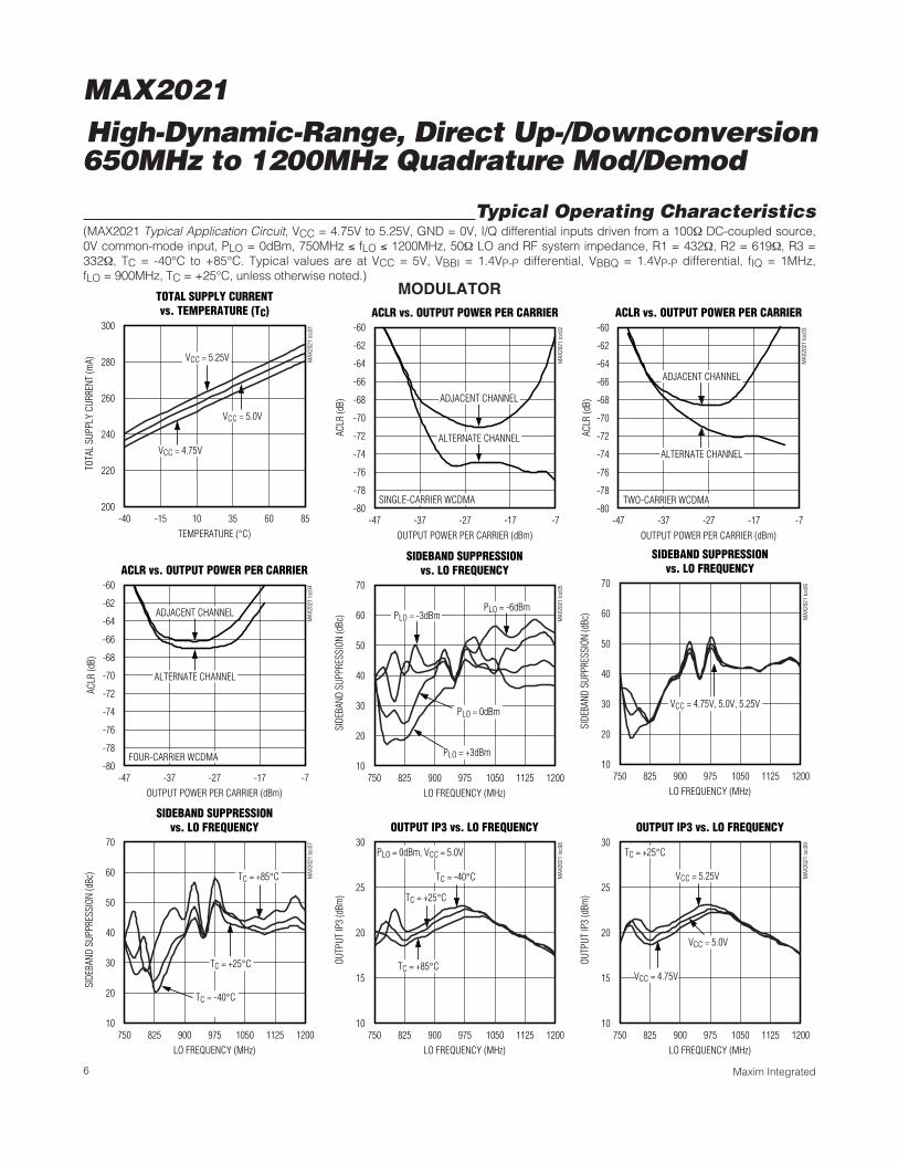
Typical Operating Characteristics(MAX2021 Typical Application Circuit, VCC = 4.75V to 5.25V, GND = 0V, I/Q differential inputs driven from a 100Ω DC-coupled source,0V common-mode input, PLO = 0dBm, 750MHz ≤ fLO ≤ 1200MHz, 50Ω LO and RF system impedance, R1 = 432Ω, R2 = 619Ω, R3 =332Ω, TC = -40°C to +85°C. Typical values are at VCC = 5V, VBBI = 1.4VP-P differential, VBBQ = 1.4VP-P differential, fIQ = 1MHz, fLO = 900MHz, TC = +25°C, unless otherwise noted.)
TOTAL SUPPLY CURRENTvs. TEMPERATURE (TC)
MAX
2021
toc0
1
TEMPERATURE (°C)
TOTA
L SU
PPLY
CUR
RENT
(mA)
603510-15
220
240
260
280
VCC = 4.75V
VCC = 5.0V
300
200-40 85
VCC = 5.25V
ACLR vs. OUTPUT POWER PER CARRIER
MAX
2021
toc0
2
OUTPUT POWER PER CARRIER (dBm)
ACLR
(dB)
-17-27-37
-78
-76
-74
-72
-70
-68
-66
-64
-62
-60
-80-47 -7
SINGLE-CARRIER WCDMA
ADJACENT CHANNEL
ALTERNATE CHANNEL
ACLR vs. OUTPUT POWER PER CARRIER
MAX
2021
toc0
3
OUTPUT POWER PER CARRIER (dBm)
ACLR
(dB)
-17-27-37
-78
-76
-74
-72
-70
-68
-66
-64
-62
-60
-80-47 -7
ADJACENT CHANNEL
ALTERNATE CHANNEL
TWO-CARRIER WCDMA
ACLR vs. OUTPUT POWER PER CARRIER
MAX
2021
toc0
4
OUTPUT POWER PER CARRIER (dBm)
ACLR
(dB)
-17-27-37
-78
-76
-74
-72
-70
-68
-66
-64
-62
-60
-80-47 -7
FOUR-CARRIER WCDMA
ADJACENT CHANNEL
ALTERNATE CHANNEL
SIDEBAND SUPPRESSIONvs. LO FREQUENCY
MAX
2021
toc0
5
LO FREQUENCY (MHz)
SIDE
BAND
SUP
PRES
SION
(dBc
)
11251050975900825
20
30
40
50
60
70
10750 1200
PLO = -3dBmPLO = -6dBm
PLO = 0dBm
PLO = +3dBm
SIDEBAND SUPPRESSIONvs. LO FREQUENCY
MAX
2021
toc0
6
LO FREQUENCY (MHz)
SIDE
BAND
SUP
PRES
SION
(dBc
)
11251050975900825
20
30
40
50
60
70
10750 1200
VCC = 4.75V, 5.0V, 5.25V
SIDEBAND SUPPRESSIONvs. LO FREQUENCY
MAX
2021
toc0
7
LO FREQUENCY (MHz)
SIDE
BAND
SUP
PRES
SION
(dBc
)
11251050975900825
20
30
40
50
60
70
10750 1200
TC = +25°C
TC = +85°C
TC = -40°C
OUTPUT IP3 vs. LO FREQUENCY
MAX
2021
toc0
8
LO FREQUENCY (MHz)
OUTP
UT IP
3 (d
Bm)
11251050975900825
15
20
25
30
10750 1200
TC = -40°C
TC = +85°C
TC = +25°C
PLO = 0dBm, VCC = 5.0V
OUTPUT IP3 vs. LO FREQUENCY
MAX
2021
toc0
9
LO FREQUENCY (MHz)
OUTP
UT IP
3 (d
Bm)
11251050975900825
15
20
25
30
10750 1200
VCC = 5.25V
VCC = 5.0V
VCC = 4.75V
TC = +25°C
MODULATOR
MAX2021High-Dynamic-Range, Direct Up-/Downconversion
650MHz to 1200MHz Quadrature Mod/Demod
7Maxim Integrated
OUTPUT IP3 vs. LO FREQUENCYM
AX20
21 to
c10
LO FREQUENCY (MHz)
OUTP
UT IP
3 (d
Bm)
11251050975900825
15
20
25
30
10750 1200
PLO = +3dBm
PLO = -3dBm
PLO = -6dBmPLO = 0dBm
TC = +25°C
OUTPUT IP3vs. COMMON-MODE VOLTAGE
MAX
2021
toc1
1
COMMON-MODE VOLTAGE (V)
OUTP
UT IP
3 (d
Bm)
1.750-1.75
21
22
23
24
25
26
20-3.50 3.50
fLO = 900MHz, PLO = 0dBm
OUTPUT IP3vs. COMMON-MODE VOLTAGE
MAX
2021
toc1
2
COMMON-MODE VOLTAGE (V)
OUTP
UT IP
3 (d
Bm)
1.750-1.75
21
22
23
24
25
26
20-3.50 3.50
fLO = 1000MHz
OUTPUT IP2 vs. LO FREQUENCY
MAX
2021
toc1
3
LO FREQUENCY (MHz)
OUTP
UT IP
2 (d
Bm)
11251050975900825
50
60
70
80
40750 1200
TC = +25°C
TC = -40°C
TC = +85°C
OUTPUT IP2 vs. LO FREQUENCYM
AX20
21 to
c14
LO FREQUENCY (MHz)
OUTP
UT IP
2 (d
Bm)
11251050975900825
50
60
70
80
40750 1200
VCC = 5.0V
VCC = 5.25V
VCC = 4.75V
OUTPUT IP2 vs. LO FREQUENCY
MAX
2021
toc1
5
LO FREQUENCY (MHz)
OUTP
UT IP
2 (d
Bm)
11251050975900825
50
60
70
80
40750 1200
PLO = +3dBm
PLO = -6dBm
PLO = -3dBm
PLO = 0dBm
OUTPUT IP2vs. COMMON-MODE VOLTAGE
MAX
2021
toc1
6
COMMON-MODE VOLTAGE (V)
OUTP
UT IP
2 (d
Bm)
1.750-1.75
60
65
70
75
80
55-3.50 3.50
fLO = 900MHz
OUTPUT IP2vs. COMMON-MODE VOLTAGE
MAX
2021
toc1
7
COMMON-MODE VOLTAGE (V)
OUTP
UT IP
2 (d
Bm)
1.750-1.75
60
55
65
70
50-3.50 3.50
fLO = 1000MHz
MODULATOR OUTPUT POWERvs. INPUT POWER
MAX
2021
toc1
8
INPUT POWER (dBm)
OUTP
UT P
OWER
(dBm
)
1916 252213
10
5
0
15
20
-510 28
INPUT SPLIT BETWEEN I AND Q,fIF = 25MHz, fLO = 900MHz
VCC = 4.75V, 5.0V, 5.25V
Typical Operating Characteristics (continued)(MAX2021 Typical Application Circuit, VCC = 4.75V to 5.25V, GND = 0V, I/Q differential inputs driven from a 100Ω DC-coupled source,0V common-mode input, PLO = 0dBm, 750MHz ≤ fLO ≤ 1200MHz, 50Ω LO and RF system impedance, R1 = 432Ω, R2 = 619Ω, R3 =332Ω, TC = -40°C to +85°C. Typical values are at VCC = 5V, VBBI = 1.4VP-P differential, VBBQ = 1.4VP-P differential, fIQ = 1MHz, fLO = 900MHz, TC = +25°C, unless otherwise noted.)
MODULATOR
MAX2021High-Dynamic-Range, Direct Up-/Downconversion 650MHz to 1200MHz Quadrature Mod/Demod
8 Maxim Integrated
MODULATOR OUTPUT POWERvs. INPUT POWER
MAX
2021
toc1
9
INPUT POWER (dBm)
OUTP
UT P
OWER
(dBm
)
1916 252213
10
5
0
15
20
-510 28
INPUT SPLIT BETWEEN I AND Q,fIF = 25MHz, fLO = 900MHz
PLO = -6dBm, -3dBm, 0dBm, +3dBm
MODULATOR OUTPUT POWERvs. LO FREQUENCY
MAX
2021
toc2
0
LO FREQUENCY (MHz)
OUTP
UT P
OWER
(dBm
)
975900 11251050825
1
-1
-3
3
5
-5750 1200
TC = -40°C
TC = +85°C TC = +25°C
VBBI = VBBQ = 1.4VP-PDIFFERENTIAL
LO LEAKAGE vs. LO FREQUENCY
MAX
2021
toc2
1
LO FREQUENCY (MHz)
LO L
EAKA
GE (d
Bm)
959948937926
-90
-80
-70
-60
-50
-40
-100915 970
PRF = -40dBm
PRF = -7dBm
PRF = -1dBm
LO LEAKAGE NULLED AT PRF = -1dBmPRF = +5dBm
LO LEAKAGE vs. LO FREQUENCY
MAX
2021
toc2
2
LO FREQUENCY (MHz)
LO L
EAKA
GE (d
Bm)
959948937926
-90
-80
-70
-60
-50
-40
-100915 970
TC = -40°C
TC = +85°C
TC = +25°C
PRF = -1dBm, LO LEAKAGE NULLED AT TC = +25°C
LO LEAKAGE vs. LO FREQUENCY
MAX
2021
toc2
3
LO FREQUENCY (MHz)
LO L
EAKA
GE (d
Bm)
959948937926
-90
-80
-70
-60
-50
-40
-100915 970
PLO = -6dBm
PLO = +3dBm
PLO = -3dBm
PLO = 0dBm
PRF = -1dBm, LO LEAKAGE NULLED AT PLO = 0dBm
OUTPUT NOISE vs. OUTPUT POWER
MAX
2021
toc2
4OUTPUT POWER (dBm)
OUTP
UT N
OISE
(dBm
/Hz)
1050-5-10
-175
-170
-165
-160
-155
-150
-180-15 15
TC = +25°C, fLO = 900MHz
PLO = -6dBm
PLO = -3dBm
PLO = 0dBm
PLO = +3dBm
OUTPUT NOISE vs. OUTPUT POWER
MAX
2021
toc2
5
OUTPUT POWER (dBm)
OUTP
UT N
OISE
(dBm
/Hz)
1050-5-10
-175
-170
-165
-160
-155
-150
-180-15 15
PLO = 0dBm, fLO = 900MHz
TC = +85°C
TC = -40°C
TC = +25°C
Typical Operating Characteristics (continued)(MAX2021 Typical Application Circuit, VCC = 4.75V to 5.25V, GND = 0V, I/Q differential inputs driven from a 100Ω DC-coupled source,0V common-mode input, PLO = 0dBm, 750MHz ≤ fLO ≤ 1200MHz, 50Ω LO and RF system impedance, R1 = 432Ω, R2 = 619Ω, R3 =332Ω, TC = -40°C to +85°C. Typical values are at VCC = 5V, VBBI = 1.4VP-P differential, VBBQ = 1.4VP-P differential, fIQ = 1MHz, fLO = 900MHz, TC = +25°C, unless otherwise noted.)
MODULATOR
MAX2021High-Dynamic-Range, Direct Up-/Downconversion
650MHz to 1200MHz Quadrature Mod/Demod
9Maxim Integrated
DEMODULATOR CONVERSION LOSSvs. LO FREQUENCY
MAX
2021
toc2
6
LO FREQUENCY (MHz)
DEM
ODUL
ATOR
CON
VERS
ION
LOSS
(dB)
975900 11251050825
10
9
8
11
12
7750 1200
PLO = 0dBm, VCC = 5.0V
TC = +85°CTC = +25°C
TC = -40°C
DEMODULATOR INPUT IP3vs. LO FREQUENCY
MAX
2021
toc2
7
LO FREQUENCY (MHz)
DEM
ODUL
ATOR
INPU
T IP
3 (d
Bm)
975900 11251050825
36
34
32
38
40
30750 1200
PLO = 0dBm, TC = +25°C
VCC = 4.75V
VCC = 5.25V
VCC = 5.0V
DEMODULATOR INPUT IP3vs. LO FREQUENCY
MAX
2021
toc2
8
LO FREQUENCY (MHz)
DEM
ODUL
ATOR
INPU
T IP
3 (d
Bm)
975900 11251050825
36
34
32
38
40
30750 1200
PLO = 0dBm, VCC = 5.0V
TC = +85°C
TC = +25°C
TC = -40°C
DEMODULATOR INPUT IP2vs. LO FREQUENCY
MAX
2021
toc2
9
LO FREQUENCY (MHz)
DEM
ODUL
ATOR
INPU
T IP
2 (d
Bm)
11251050975900825
60
70
80
90
50750 1200
TC = -40°C
TC = +85°C
TC = +25°C
PLO = 0dBm, VCC = 5.0V
DEMODULATOR PHASE IMBALANCEvs. LO FREQUENCY
MAX
2021
toc3
0
DEM
ODUL
ATOR
PHA
SE IM
BALA
NCE
(deg
)
-8
-6
-4
-2
0
2
4
6
8
10
-10
LO FREQUENCY (MHz)11251050975900825750 1200
PLO = -3dBm
PLO = 0dBm
PLO = +3dBm
PLO = -6dBm
MAX
2021
toc3
1
-0.15
-0.10
-0.05
0
0.05
0.10
0.15
0.20
-0.20
DEMODULATOR AMPLITUDE IMBALANCEvs. LO FREQUENCY
DEM
ODUL
ATOR
AM
PLIT
UDE
IMBA
LANC
E (d
B)
LO FREQUENCY (MHz)11251050975900825750 1200
PLO = -6dBm, -3dBm, 0dBm, +3dBm
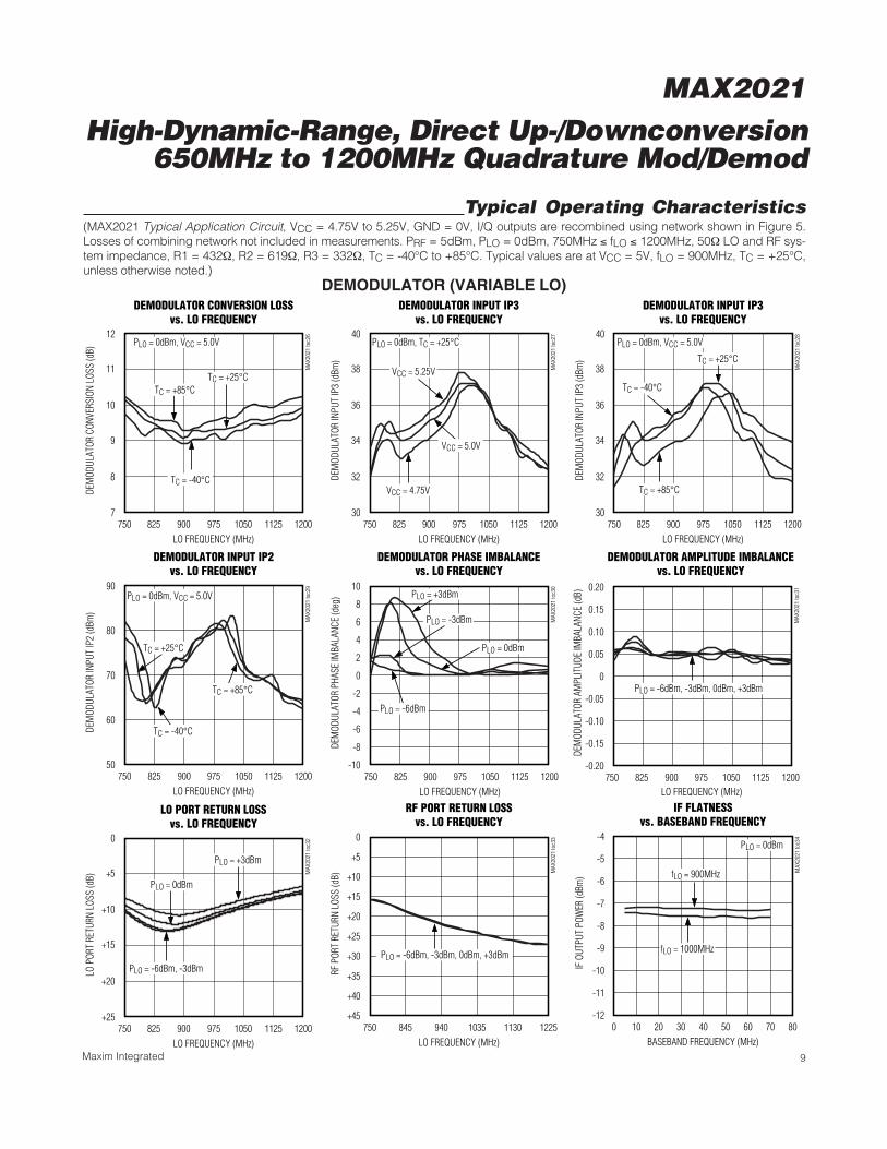
Typical Operating Characteristics(MAX2021 Typical Application Circuit, VCC = 4.75V to 5.25V, GND = 0V, I/Q outputs are recombined using network shown in Figure 5.Losses of combining network not included in measurements. PRF = 5dBm, PLO = 0dBm, 750MHz ≤ fLO ≤ 1200MHz, 50Ω LO and RF sys-tem impedance, R1 = 432Ω, R2 = 619Ω, R3 = 332Ω, TC = -40°C to +85°C. Typical values are at VCC = 5V, fLO = 900MHz, TC = +25°C,unless otherwise noted.)
LO PORT RETURN LOSSvs. LO FREQUENCY
MAX
2021
toc3
2
LO FREQUENCY (MHz)
LO P
ORT
RETU
RN L
OSS
(dB)
975900 11251050825
+10
+15
+20
+5
0
+25750 1200
PLO = -6dBm, -3dBm
PLO = +3dBm
PLO = 0dBm
RF PORT RETURN LOSSvs. LO FREQUENCY
MAX
2021
toc3
3
LO FREQUENCY (MHz)
RF P
ORT
RETU
RN L
OSS
(dB)
11301035940845
+40
+35
+30
+25
+20
+15
+10
+5
0
+45750 1225
PLO = -6dBm, -3dBm, 0dBm, +3dBm
IF FLATNESSvs. BASEBAND FREQUENCY
MAX
2021
toc3
4
BASEBAND FREQUENCY (MHz)
IF O
UTPU
T PO
WER
(dBm
)
706010 20 30 40 50
-11
-10
-9
-8
-7
-6
-5
-4
-120 80
fLO = 1000MHz
fLO = 900MHz
PLO = 0dBm
DEMODULATOR (VARIABLE LO)
MAX2021High-Dynamic-Range, Direct Up-/Downconversion 650MHz to 1200MHz Quadrature Mod/Demod
10 Maxim Integrated
CONVERSION LOSS vs. RF FREQUENCYM
AX20
21 to
c35
RF FREQUENCY (MHz)
CONV
ERSI
ON L
OSS
(dB)
830785740695
8
9
10
11
12
7650 875
fLO = 965MHz
I/Q GAIN MISMATCH vs. IF FREQUENCY
MAX
2021
toc3
6
IF FREQUENCY (MHz)
GAIN
MIS
MAT
CH (
dB)
270225180135
-0.05
0
0.05
0.10
-0.1090 315
fLO = 965MHz
I/Q PHASE MISMATCH vs. IF FREQUENCY
MAX
2021
toc3
7
IF FREQUENCY (MHz)
PHAS
E M
ISM
ATCH
(DE
G)
270225180135
-0.5
0
0.5
1.0
1.5
2.0
-1.090 315
fLO = 965MHz
INPUT IP3 vs. RF FREQUENCY
MAX
2021
toc3
8
RF FREQUENCY (MHz)
INPU
T IP
3 (d
Bm)
875800725
33
34
35
36
37
38
32650 950
PRF = 0dBm/TONEfLO = 965MHz
1MHz TONE DELTA
45MHz TONE DELTA
INPUT IP2 vs. RF FREQUENCY
MAX
2021
toc3
9
RF FREQUENCY (MHz)
INPU
T IP
2 (d
Bm)
875800725
65
70
75
80
85
90
60650 950
1MHz TONE DELTA
45MHz TONE DELTA
PRF = 0dBm/TONEfLO = 965MHz
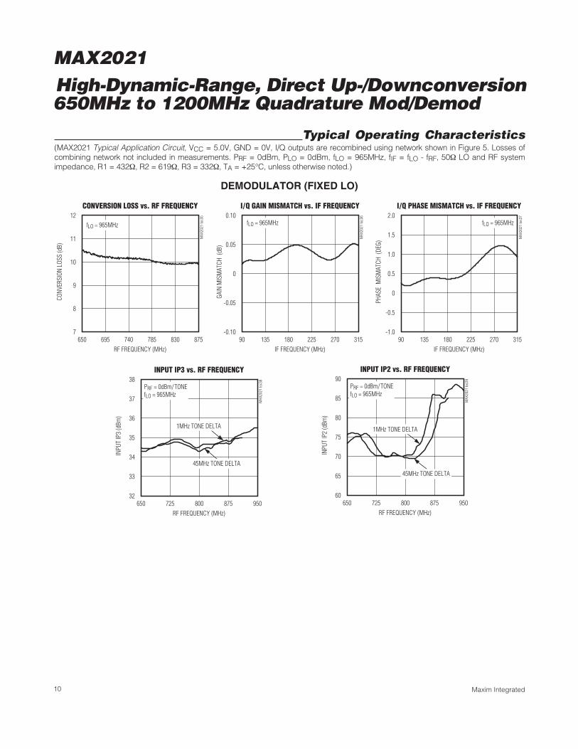
Typical Operating Characteristics(MAX2021 Typical Application Circuit, VCC = 5.0V, GND = 0V, I/Q outputs are recombined using network shown in Figure 5. Losses ofcombining network not included in measurements. PRF = 0dBm, PLO = 0dBm, fLO = 965MHz, fIF = fLO - fRF, 50Ω LO and RF systemimpedance, R1 = 432Ω, R2 = 619Ω, R3 = 332Ω, TA = +25°C, unless otherwise noted.)
DEMODULATOR (FIXED LO)
MAX2021High-Dynamic-Range, Direct Up-/Downconversion
650MHz to 1200MHz Quadrature Mod/Demod
11Maxim Integrated
Detailed DescriptionThe MAX2021 is designed for upconverting differentialin-phase (I) and quadrature (Q) inputs from basebandto a 650MHz to 1200MHz RF frequency range. Thedevice can also be used as a demodulator, downcon-verting an RF input signal directly to baseband.Applications include RFID handheld and portal readers,as well as single and multicarrier GSM/EDGE,cdma2000, WCDMA, and iDEN base stations. Directconversion architectures are advantageous since theysignificantly reduce transmitter or receiver cost, partcount, and power consumption as compared to tradition-al IF-based double conversion systems.
The MAX2021 integrates internal baluns, an LO buffer, aphase splitter, two LO driver amplifiers, two matcheddouble-balanced passive mixers, and a widebandquadrature combiner. The MAX2021’s high-linearity mix-ers, in conjunction with the part’s precise in-phase andquadrature channel matching, enable the device to pos-sess excellent dynamic range, ACLR, 1dB compression
point, and LO and sideband suppression characteris-tics. These features make the MAX2021 ideal for four-carrier WCDMA operation.
LO Input Balun, LO Buffer, and Phase Splitter
The MAX2021 requires a single-ended LO input, with anominal power of 0dBm. An internal low-loss balun atthe LO input converts the single-ended LO signal to adifferential signal at the LO buffer input. In addition, theinternal balun matches the buffer’s input impedance to50Ω over the entire band of operation.
The output of the LO buffer goes through a phase split-ter, which generates a second LO signal that is shiftedby 90° with respect to the original. The 0° and 90° LOsignals drive the I and Q mixers, respectively.
LO DriverFollowing the phase splitter, the 0° and 90° LO signalsare each amplified by a two-stage amplifier to drive theI and Q mixers. The amplifier boosts the level of the LO
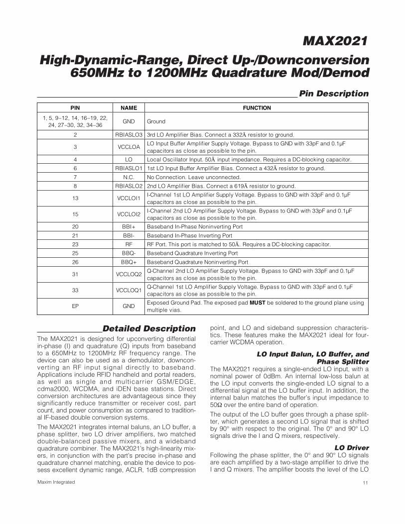
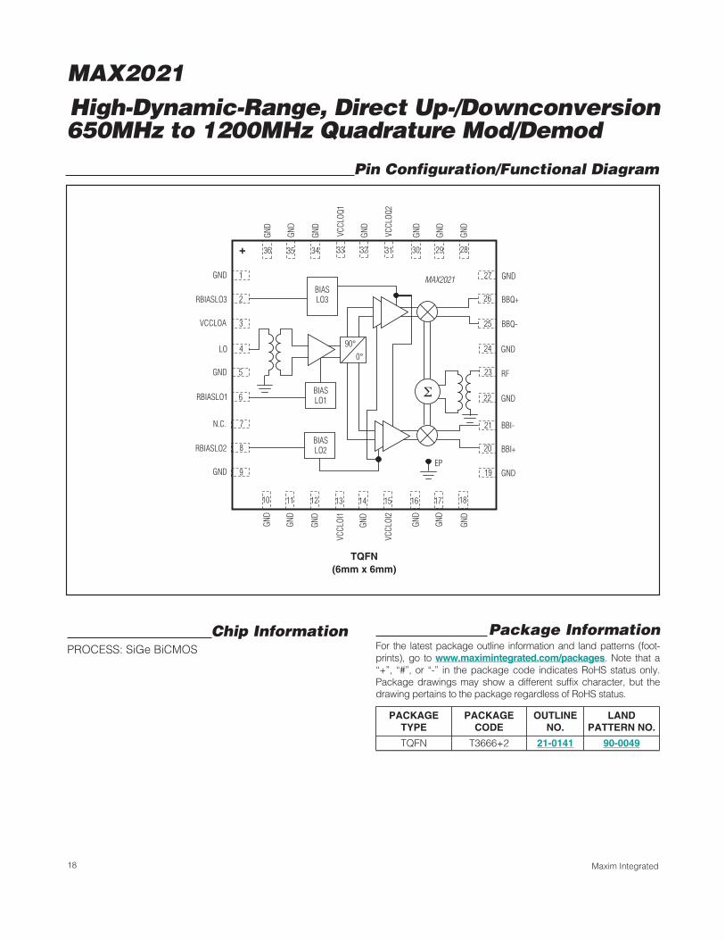
Pin Description
PIN NAME FUNCTION
1, 5, 9–12, 14, 16–19, 22, 24, 27–30, 32, 34–36
GND Ground
2 RBIASLO3 3rd LO Amplifier Bias. Connect a 332Ā resistor to ground.
3 VCCLOA LO Input Buffer Amplifier Supply Voltage. Bypass to GND with 33pF and 0.1µF capacitors as close as possible to the pin.
4 LO Local Oscillator Input. 50Ā input impedance. Requires a DC-blocking capacitor.
6 RBIASLO1 1st LO Input Buffer Amplifier Bias. Connect a 432Ā resistor to ground.
7 N.C. No Connection. Leave unconnected.
8 RBIASLO2 2nd LO Amplifier Bias. Connect a 619Ā resistor to ground.
13 VCCLOI1 I-Channel 1st LO Amplifier Supply Voltage. Bypass to GND with 33pF and 0.1µF capacitors as close as possible to the pin.
15 VCCLOI2 I-Channel 2nd LO Amplifier Supply Voltage. Bypass to GND with 33pF and 0.1µF capacitors as close as possible to the pin.
20 BBI+ Baseband In-Phase Noninverting Port
21 BBI- Baseband In-Phase Inverting Port
23 RF RF Port. This port is matched to 50Ā. Requires a DC-blocking capacitor.
25 BBQ- Baseband Quadrature Inverting Port
26 BBQ+ Baseband Quadrature Noninverting Port
31 VCCLOQ2 Q-Channel 2nd LO Amplifier Supply Voltage. Bypass to GND with 33pF and 0.1µF capacitors as close as possible to the pin.
33 VCCLOQ1 Q-Channel 1st LO Amplifier Supply Voltage. Bypass to GND with 33pF and 0.1µF capacitors as close as possible to the pin.
EP GND Exposed Ground Pad. The exposed pad MUST be soldered to the ground plane using multiple vias.
MAX2021High-Dynamic-Range, Direct Up-/Downconversion 650MHz to 1200MHz Quadrature Mod/Demod
12 Maxim Integrated
signals to compensate for any changes in LO drive lev-els. The two-stage LO amplifier allows a wide inputpower range for the LO drive. The MAX2021 can toler-ate LO level swings from -6dBm to +3dBm.
I/Q ModulatorThe MAX2021 modulator is composed of a pair ofmatched double-balanced passive mixers and a balun.The I and Q differential baseband inputs accept signalsfrom DC to 550MHz with differential amplitudes up to4VP-P. The wide input bandwidths allow operation of theMAX2021 as either a direct RF modulator or as animage-reject mixer. The wide common-mode compli-ance range allows for direct interface with the base-band DACs. No active buffer circuitry is requiredbetween the baseband DACs and the MAX2021 forcdma2000 and WCDMA applications.
The I and Q signals directly modulate the 0° and 90° LOsignals and are upconverted to the RF frequency. The out-puts of the I and Q mixers are combined through a balunto produce a singled-ended RF output.
Applications InformationLO Input Drive
The LO input of the MAX2021 is internally matched to50Ω, and requires a single-ended drive at a 750MHz to1200MHz frequency range. An integrated balun con-verts the singled-ended input signal to a differential sig-nal at the LO buffer differential input. An externalDC-blocking capacitor is the only external part requiredat this interface. The LO input power should be withinthe -6dBm to +3dBm range. An LO input power of -3dBm is recommended for best overall peformance.
Modulator Baseband I/Q Input DriveDrive the MAX2021 I and Q baseband inputs differen-tially for best performance. The baseband inputs havea 53Ω differential input impedance. The optimumsource impedance for the I and Q inputs is 100Ω differ-ential. This source impedance achieves the optimal sig-nal transfer to the I and Q inputs, and the optimumoutput RF impedance match. The MAX2021 can acceptinput power levels of up to +20dBm on the I and Qinputs. Operation with complex waveforms, such asCDMA carriers or GSM signals, utilize input power lev-els that are far lower. This lower power operation ismade necessary by the high peak-to-average ratios ofthese complex waveforms. The peak signals must bekept below the compression level of the MAX2021.
The four baseband ports need some form of DC returnto establish a common mode that the on-chip circuitrydrives. This can be achieved by directly DC-coupling tothe baseband ports (staying within the ±3.5V common-
mode range), through an inductor to ground, or througha low-value resistor to ground.
The MAX2021 is designed to interface directly withMaxim high-speed DACs. This generates an ideal totaltransmitter lineup, with minimal ancillary circuit elements.Such DACs include the MAX5875 series of dual DACs,and the MAX5895 dual interpolating DAC. These DACshave ground-referenced differential current outputs.Typical termination of each DAC output into a 50Ω loadresistor to ground, and a 10mA nominal DC output cur-rent results in a 0.5V common-mode DC level into themodulator I/Q inputs. The nominal signal level providedby the DACs will be in the -12dBm range for a singleCDMA or WCDMA carrier, reducing to -18dBm per car-rier for a four-carrier application.
The I/Q input bandwidth is greater than 50MHz at -0.1dB response. The direct connection of the DAC tothe MAX2021 ensures the maximum signal fidelity, withno performance-limiting baseband amplifiers required.The DAC output can be passed through a lowpass filterto remove the image frequencies from the DAC’s outputresponse. The MAX5895 dual interpolating DAC can beoperated at interpolation rates up to x8. This has thebenefit of moving the DAC image frequencies to a veryhigh, remote frequency, easing the design of the base-band filters. The DAC’s output noise floor and interpola-tion filter stopband attenuation are sufficiently good toensure that the 3GPP noise floor requirement is met forlarge frequency offsets, 60MHz for example, with no fil-tering required on the RF output of the modulator.
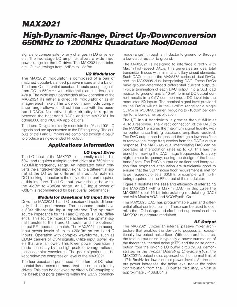
Figure 1 illustrates the ease and efficiency of interfacingthe MAX2021 with a Maxim DAC (in this case theMAX5895 dual 16-bit interpolating-modulating DAC)and with Maxim VGA and VCO/Synth ICs.
The MAX5895 DAC has programmable gain and differ-ential offset controls built in. These can be used to opti-mize the LO leakage and sideband suppression of theMAX2021 quadrature modulator.
RF OutputThe MAX2021 utilizes an internal passive mixer archi-tecture that enables the device to possess an excep-tionally low-output noise floor. With such architectures,the total output noise is typically a power summation ofthe theoretical thermal noise (KTB) and the noise contri-bution from the on-chip LO buffer circuitry. As demon-strated in the Typical Operating Characteristics, theMAX2021’s output noise approaches the thermal limit of-174dBm/Hz for lower output power levels. As the out-put power increases, the noise level tracks the noisecontribution from the LO buffer circuitry, which isapproximately -168dBc/Hz.
MAX2021High-Dynamic-Range, Direct Up-/Downconversion
650MHz to 1200MHz Quadrature Mod/Demod
13Maxim Integrated
The I/Q input power levels and the insertion loss of thedevice determine the RF output power level. The inputpower is a function of the delivered input I and Q volt-ages to the internal 50Ω termination. For simple sinu-soidal baseband signals, a level of 89mVP-P differentialon the I and the Q inputs results in a -17dBm inputpower level delivered to the I and Q internal 50Ω termi-nations. This results in an RF output power of -23.2dBm.
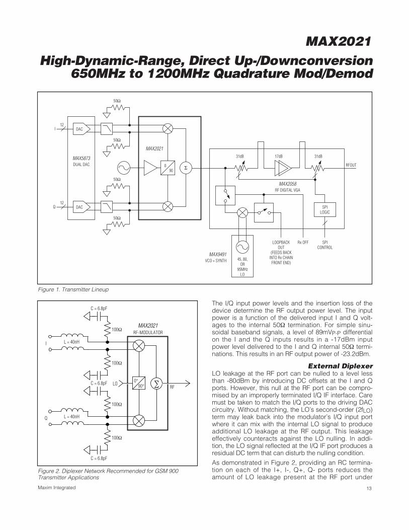
External DiplexerLO leakage at the RF port can be nulled to a level lessthan -80dBm by introducing DC offsets at the I and Qports. However, this null at the RF port can be compro-mised by an improperly terminated I/Q IF interface. Caremust be taken to match the I/Q ports to the driving DACcircuitry. Without matching, the LO’s second-order (2fLO)term may leak back into the modulator’s I/Q input portwhere it can mix with the internal LO signal to produceadditional LO leakage at the RF output. This leakageeffectively counteracts against the LO nulling. In addi-tion, the LO signal reflected at the I/Q IF port produces aresidual DC term that can disturb the nulling condition.
As demonstrated in Figure 2, providing an RC termina-tion on each of the I+, I-, Q+, Q- ports reduces theamount of LO leakage present at the RF port under
RF-MODULATOR
LORF
100Ω
100Ω
L = 40nH
C = 6.8pF
∑
L = 40nH
I
Q
100Ω
100Ω
C = 6.8pF
C = 6.8pF
0°90°
MAX2021
Figure 2. Diplexer Network Recommended for GSM 900Transmitter Applications
12I DAC
50I
31dB 31dB17dB
RFOUT
50I
12Q DAC
50I
50I
090 C
MAX2021
MAX5873DUAL DAC
45, 80,OR
95MHzLO
LOOPBACKOUT
(FEEDS BACKINTO Rx CHAIN
FRONT END)
Rx OFF SPICONTROL
SPILOGIC
MAX2058RF DIGITAL VGA
MAX9491VCO + SYNTH
Figure 1. Transmitter Lineup
MAX2021High-Dynamic-Range, Direct Up-/Downconversion 650MHz to 1200MHz Quadrature Mod/Demod
14 Maxim Integrated
varying temperature, LO frequency, and basebanddrive conditions. See the Typical OperatingCharacteristics for details. Note that the resistor value ischosen to be 100Ω with a corner frequency 1 / (2πRC)selected to adequately filter the fLO and 2fLO leakage,yet not affecting the flatness of the baseband responseat the highest baseband frequency. The common-mode fLO and 2fLO signals at I+/I- and Q+/Q- effective-ly see the RC networks and thus become terminated in50Ω (R/2). The RC network provides a path for absorb-ing the 2fLO and fLO leakage, while the inductor pro-vides high impedance at fLO and 2fLO to help thediplexing process.
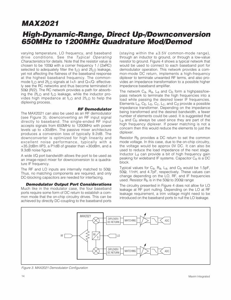
RF DemodulatorThe MAX2021 can also be used as an RF demodulator(see Figure 3), downconverting an RF input signaldirectly to baseband. The single-ended RF inputaccepts signals from 650MHz to 1200MHz with powerlevels up to +30dBm. The passive mixer architectureproduces a conversion loss of typically 9.2dB. Thedownconverter is optimized for high linearity andexcellent noise performance, typical ly with a+35.2dBm IIP3, a P1dB of greater than +30dBm, and a9.3dB noise figure.
A wide I/Q port bandwidth allows the port to be used asan image-reject mixer for downconversion to a quadra-ture IF frequency.
The RF and LO inputs are internally matched to 50Ω.Thus, no matching components are required, and onlyDC-blocking capacitors are needed for interfacing.
Demodulator Output Port ConsiderationsMuch like in the modulator case, the four basebandports require some form of DC return to establish a com-mon mode that the on-chip circuitry drives. This can beachieved by directly DC-coupling to the baseband ports
(staying within the ±3.5V common-mode range),through an inductor to ground, or through a low-valueresistor to ground. Figure 4 shows a typical network thatwould be used to connect to each baseband port fordemodulator operation. This network provides a com-mon-mode DC return, implements a high-frequencydiplexer to terminate unwanted RF terms, and also pro-vides an impedance transformation to a possible higherimpedance baseband amplifier.
The network Ca, Ra, La and Cb form a highpass/low-pass network to terminate the high frequencies into aload while passing the desired lower IF frequencies.Elements La, Cb, Lb, Cc, Lc, and Cd provide a possibleimpedance transformer. Depending on the impedancebeing transformed and the desired bandwidth, a fewernumber of elements could be used. It is suggested thatLa and Cb always be used since they are part of thehigh frequency diplexer. If power matching is not aconcern then this would reduce the elements to just thediplexer.
Resistor Rb provides a DC return to set the commonmode voltage. In this case, due to the on-chip circuitry,the voltage would be approx 0V DC. It can also beused to reduce the load impedance of the next stage.Inductor Ld can provide a bit of high frequency gainpeaking for wideband IF systems. Capacitor Ce is a DCblock.
Typical values for Ca, Ra, La, and Cb would be 1.5pF,50Ω, 11nH, and 4.7pF, respectively. These values canchange depending on the LO, RF, and IF frequenciesused. Resistor Rb is in the 50Ω to 200Ω range
The circuitry presented in Figure 4 does not allow for LOleakage at RF port nulling. Depending on the LO at RFleakage requirement, a trim voltage might need to beintroduced on the baseband ports to null the LO leakage.
ADC
900RF LO
MAX2021DIPLEXER/DC RETURN
MATCHING
ADCDIPLEXER/DC RETURN
MATCHING
Figure 3. MAX2021 Demodulator Configuration

MAX2021High-Dynamic-Range, Direct Up-/Downconversion
650MHz to 1200MHz Quadrature Mod/Demod
15Maxim Integrated
EXTERNALSTAGE
La
Ra
Cb Cc Cd
CaLb
Rb
Lc
Ld
Ce
MAX2021I/Q OUTPUTS
Figure 4. Baseband Port Typical Filtering and DC Return Network
3dB PAD DC BLOCK 0°
3dB PAD DC BLOCK 180°
MINI-CIRCUITSZFSC-2-1W-S+0° COMBINER
3dB PADS LOOK LIKE 160I TO GROUNDAND PROVIDES THE COMMON-MODE
DC RETURN FOR THE ON-CHIP CIRCUITRY.
I+
I-
3dB PAD DC BLOCK 0°
3dB PAD DC BLOCK 180°
MINI-CIRCUITSZFSCJ-2-1
MINI-CIRCUITSZFSCJ-2-1
Q+
Q-
90°
Figure 5. Demodulator Combining Diagram
Power Scaling with Changesto the Bias Resistors
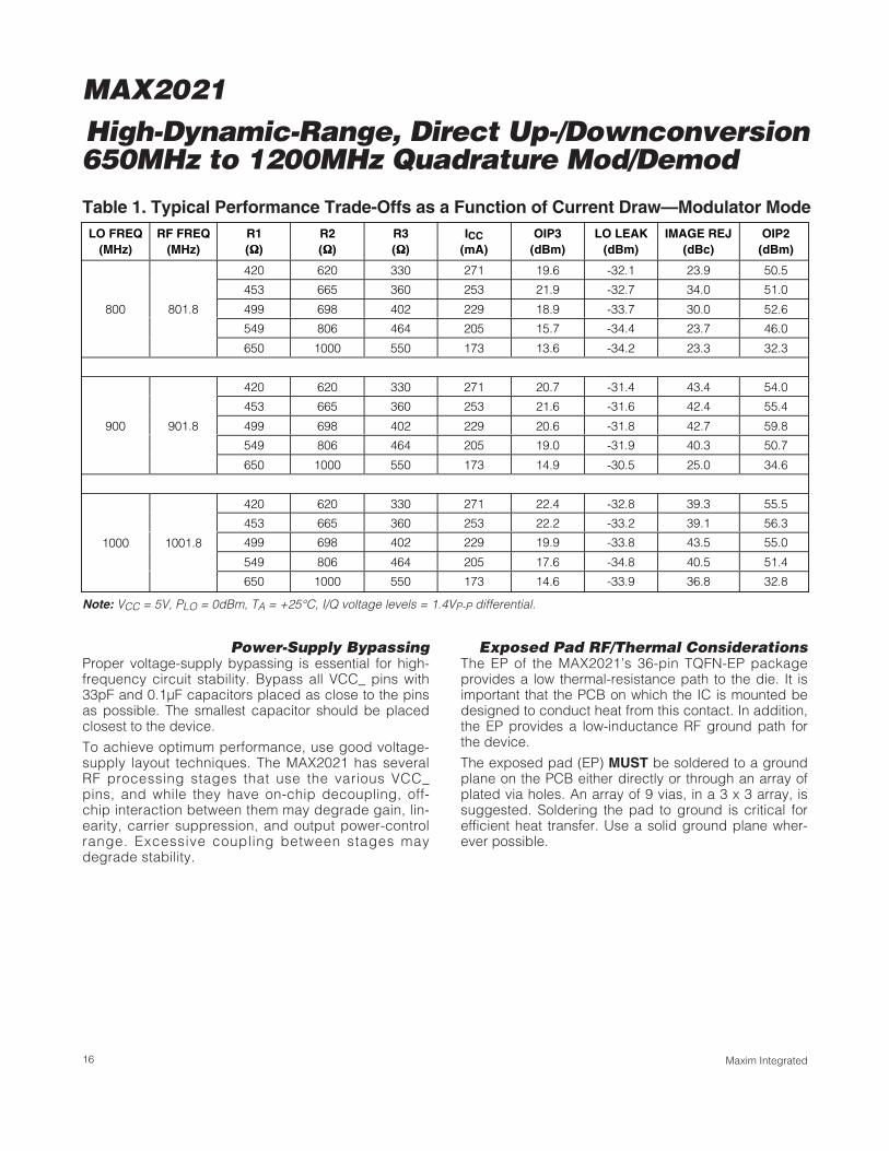
Bias currents for the LO buffers are optimized by finetuning resistors R1, R2, and R3. Maxim recommendsusing ±1%-tolerance resistors; however, standard ±5%values can be used if the ±1% components are notreadily available. The resistor values shown in theTypical Application Circuit were chosen to providepeak performance for the entire 650MHz to 1200MHzband. If desired, the current can be backed off fromthis nominal value by choosing different values for R1,R2, and R3. Tables 1 and 2 outline the performancetrade-offs that can be expected for various combina-tions of these bias resistors. As noted within the tables,the performance trade-offs may be more pronouncedfor different operating frequencies. Contact the factoryfor additional details.
Layout ConsiderationsA properly designed PCB is an essential part of anyRF/microwave circuit. Keep RF signal lines as short aspossible to reduce losses, radiation, and inductance.For the best performance, route the ground pin tracesdirectly to the exposed pad under the package. ThePCB exposed pad MUST be connected to the groundplane of the PCB. It is suggested that multiple vias beused to connect this pad to the lower-level groundplanes. This method provides a good RF/thermal con-duction path for the device. Solder the exposed pad onthe bottom of the device package to the PCB. TheMAX2021 evaluation kit can be used as a reference forboard layout. Gerber files are available upon request atwww.maximintegrated.com.
MAX2021High-Dynamic-Range, Direct Up-/Downconversion 650MHz to 1200MHz Quadrature Mod/Demod
16 Maxim Integrated
Note: VCC = 5V, PLO = 0dBm, TA = +25°C, I/Q voltage levels = 1.4VP-P differential.
LO FREQ(MHz)
RF FREQ(MHz)
R1(ΩΩΩΩ)
R2(ΩΩΩΩ)
R3(ΩΩΩΩ)
ICC(mA)
OIP3(dBm)
LO LEAK(dBm)
IMAGE REJ(dBc)
OIP2(dBm)
420 620 330 271 19.6 -32.1 23.9 50.5
453 665 360 253 21.9 -32.7 34.0 51.0
499 698 402 229 18.9 -33.7 30.0 52.6
549 806 464 205 15.7 -34.4 23.7 46.0
800 801.8
650 1000 550 173 13.6 -34.2 23.3 32.3
420 620 330 271 20.7 -31.4 43.4 54.0
453 665 360 253 21.6 -31.6 42.4 55.4
499 698 402 229 20.6 -31.8 42.7 59.8
549 806 464 205 19.0 -31.9 40.3 50.7
900 901.8
650 1000 550 173 14.9 -30.5 25.0 34.6
420 620 330 271 22.4 -32.8 39.3 55.5
453 665 360 253 22.2 -33.2 39.1 56.3
499 698 402 229 19.9 -33.8 43.5 55.0
549 806 464 205 17.6 -34.8 40.5 51.4
1000 1001.8
650 1000 550 173 14.6 -33.9 36.8 32.8
Table 1. Typical Performance Trade-Offs as a Function of Current Draw—Modulator Mode
Power-Supply BypassingProper voltage-supply bypassing is essential for high-frequency circuit stability. Bypass all VCC_ pins with33pF and 0.1µF capacitors placed as close to the pinsas possible. The smallest capacitor should be placedclosest to the device.
To achieve optimum performance, use good voltage-supply layout techniques. The MAX2021 has severalRF processing stages that use the various VCC_pins, and while they have on-chip decoupling, off-chip interaction between them may degrade gain, lin-earity, carrier suppression, and output power-controlrange. Excessive coupling between stages maydegrade stability.
Exposed Pad RF/Thermal ConsiderationsThe EP of the MAX2021’s 36-pin TQFN-EP packageprovides a low thermal-resistance path to the die. It isimportant that the PCB on which the IC is mounted bedesigned to conduct heat from this contact. In addition,the EP provides a low-inductance RF ground path forthe device.
The exposed pad (EP) MUST be soldered to a groundplane on the PCB either directly or through an array ofplated via holes. An array of 9 vias, in a 3 x 3 array, issuggested. Soldering the pad to ground is critical forefficient heat transfer. Use a solid ground plane wher-ever possible.

MAX2021High-Dynamic-Range, Direct Up-/Downconversion
650MHz to 1200MHz Quadrature Mod/Demod
17Maxim Integrated
LO FREQ(MHz)
RF FREQ(MHz)
R1(ΩΩΩΩ)
R2(ΩΩΩΩ)
R3(ΩΩΩΩ)
ICC(mA)
C O N VER SIO N L O SS ( d B )
IIP3(dBm)
57MHz IIP2(dBm)
420 620 330 269 9.8 33.85 62.1
453 665 360 254 9.83 33.98 62.9
499 698 402 230 9.81 32.2 66.6
549 806 464 207 9.84 31.1 66.86
800 771
650 1000 550 173 9.95 29.87 65.25
420 620 330 269 9.21 33.1 68
453 665 360 254 9.25 33.9 66.87
499 698 402 230 9.36 34.77 66.7
549 806 464 207 9.39 35.3 66.6
900 871
650 1000 550 173 9.46 32 64.64
420 620 330 269 9.47 34.9 > 77.7
453 665 360 254 9.5 35.4 > 77.5
499 698 402 230 9.53 34.58 > 76.5
549 806 464 207 9.5 33.15 > 76.5
1000 971
650 1000 550 173 9.61 31.5 76
Table 2. Typical Performance Trade-Offs as a Function of Current Draw—Demodulator Mode
Note: Used on PCB 180° combiners and off PCB quadrature combiner with VCC = 5V, PRF = -3dBm, PLO = 0dBm, TA = +25°C,IF1 = 28MHz, IF2 = 29MHz.
MAX2021High-Dynamic-Range, Direct Up-/Downconversion 650MHz to 1200MHz Quadrature Mod/Demod
18 Maxim Integrated
Chip InformationPROCESS: SiGe BiCMOS
1
2
3
4
5
6
7
8
9
10 11 12 13 14
TQFN(6mm x 6mm)
15 16 17 18
27
26
25
24
23
22
21
20
19
36 35 34 33 32 31 30 29 28
Σ
BIASLO2
BIASLO1
90°0°
BIASLO3
GND
BBI+
BBI-
GND
RF
GND
BBQ-
BBQ+
GNDGN
D
GND
GND
GND
GND
GND
GND
GND
GND
+
RBIASLO3
VCCLOA
LO
GND
RBIASLO1
N.C.
RBIASLO2
GND
GND
GND
VCCL
OQ2
GND
GND
GND
GND
MAX2021
VCCL
OI1
VCCL
OI2
VCCL
OQ1
EP
Pin Configuration/Functional Diagram
PACKAGETYPE
PACKAGECODE
OUTLINENO.
LANDPATTERN NO.
TQFN T3666+2 21-0141 90-0049
Package InformationFor the latest package outline information and land patterns (foot-prints), go to www.maximintegrated.com/packages. Note that a“+”, “#”, or “-” in the package code indicates RoHS status only.Package drawings may show a different suffix character, but thedrawing pertains to the package regardless of RoHS status.

MAX2021High-Dynamic-Range, Direct Up-/Downconversion
650MHz to 1200MHz Quadrature Mod/Demod
19Maxim Integrated
1
2
3
4
5
6
7
8
9
10 11 12 13 14 15 16 17 18
EP
27
26
25
24
23
22
21
20
19
36 35 34 33 32 31 30 29 28
Σ
BIASLO2
BIASLO1
90°0°
BIASLO3
GND
BBI+
BBI-
GND
RFRF
GND
BBQ-
BBQ+Q+
Q-
GND
I-
I+
C98.2pF
C80.1µF
VCCC733pF
C50.1µF
C633pF
VCC
GND GND GND GND
VCCL
OI1
VCCL
OI2
GND GND GND
GND
GND
RBIASLO3
R3332Ω
C133pF
C382pF
C20.1µF
VCCVCCLOA
LOLO
GND
RBIASLO1
R1432Ω
N.C.
RBIASLO2
C110.1µF
VCC
C1033pF
C120.1µF
C1333pFVCC
GNDGNDGNDVCCL
OQ2
GNDGNDGNDGND
MAX2021
VCCL
OQ1
R2619Ω
+
Typical Application Circuit
COMPONENT VALUE DESCRIPTION
C1, C6, C7, C10, C13 33pF 33pF ±5%, 50V C0G ceramic capacitors (0402)
C2, C5, C8, C11, C12 0.1µF 0.1µF ±10%, 16V X7R ceramic capacitors (0603)
C3 82pF 82pF ±5%, 50V C0G ceramic capacitor (0402)
C9 8.2pF 8.2pF ±0.1pF, 50V C0G ceramic capacitor (0402)
R1 432Ω 432Ω ±1% resistor (0402)
R2 619Ω 619Ω ±1% resistor (0402)
R3 332Ω 332Ω ±1% resistor (0402)
Table 3. Component List Referring to the Typical Application Circuit
Maxim Integrated cannot assume responsibility for use of any circuitry other than circuitry entirely embodied in a Maxim Integrated product. No circuit patentlicenses are implied. Maxim Integrated reserves the right to change the circuitry and specifications without notice at any time. The parametric values (min andmax limits) shown in the Electrical Characteristics table are guaranteed. Other parametric values quoted in this data sheet are provided for guidance.
20 ________________________________Maxim Integrated 160 Rio Robles, San Jose, CA 95134 USA 1-408-601-1000
© 2013 Maxim Integrated Products, Inc. Maxim Integrated and the Maxim Integrated logo are trademarks of Maxim Integrated Products, Inc.
MAX2021High-Dynamic-Range, Direct Up-/Downconversion 650MHz to 1200MHz Quadrature Mod/Demod
Revision HistoryREVISION NUMBER
REVISION DATE
DESCRIPTIONPAGES
CHANGED
0 7/06 Initial release —
1 6/12
Updated Features section; updated Ordering Information, Absolute Maximum Ratings,DC Electrical Characteristics, Pin Description, AC Electrical Characteristics table, Typical Operating Characteristics globals, Detailed Description section, I/Q Modulatorsection, Baseband I/Q Input Drive section, Power Scaling with the Changes to the Bias Resistors section, Typical Application Circuit, Figures 1–3, and Table 1
1–3, 9–11, 14
2 4/13 Updated Electrical Characteristics table; updated TOCs 35–39; updated title and Features section
1, 2, 4, 8, 9, 12, 13