MAX II Device Handbook - Farnell element14 chapters contain feature definitions of the internal...
88
© August 2009 Altera Corporation MAX II Device Handbook Section I. MAX II Device Family Data Sheet This section provides designers with the data sheet specifications for MAX ® II devices. The chapters contain feature definitions of the internal architecture, Joint Test Action Group (JTAG) and in-system programmability (ISP) information, DC operating conditions, AC timing parameters, and ordering information for MAX II devices. This section includes the following chapters: ■ Chapter 1, Introduction ■ Chapter 2, MAX II Architecture ■ Chapter 3, JTAG and In-System Programmability ■ Chapter 4, Hot Socketing and Power-On Reset in MAX II Devices ■ Chapter 5, DC and Switching Characteristics ■ Chapter 6, Reference and Ordering Information Revision History Refer to each chapter for its own specific revision history. For information about when each chapter was updated, refer to the Chapter Revision Dates section, which appears in the complete handbook.
Transcript of MAX II Device Handbook - Farnell element14 chapters contain feature definitions of the internal...

© August 2009 Altera Corporation
Section I. MAX II Device Family DataSheet
This section provides designers with the data sheet specifications for MAX® II devices. The chapters contain feature definitions of the internal architecture, Joint Test Action Group (JTAG) and in-system programmability (ISP) information, DC operating conditions, AC timing parameters, and ordering information for MAX II devices.
This section includes the following chapters:
■ Chapter 1, Introduction
■ Chapter 2, MAX II Architecture
■ Chapter 3, JTAG and In-System Programmability
■ Chapter 4, Hot Socketing and Power-On Reset in MAX II Devices
■ Chapter 5, DC and Switching Characteristics
■ Chapter 6, Reference and Ordering Information
Revision History Refer to each chapter for its own specific revision history. For information about when each chapter was updated, refer to the Chapter Revision Dates section, which appears in the complete handbook.
MAX II Device Handbook

I–2 Section I: MAX II Device Family Data SheetRevision History
MAX II Device Handbook © August 2009 Altera Corporation

© August 2009 Altera Corporation
MII51001-1.9
1. Introduction
IntroductionThe MAX® II family of instant-on, non-volatile CPLDs is based on a 0.18-µm, 6-layer-metal-flash process, with densities from 240 to 2,210 logic elements (LEs) (128 to 2,210 equivalent macrocells) and non-volatile storage of 8 Kbits. MAX II devices offer high I/O counts, fast performance, and reliable fitting versus other CPLD architectures. Featuring MultiVolt core, a user flash memory (UFM) block, and enhanced in-system programmability (ISP), MAX II devices are designed to reduce cost and power while providing programmable solutions for applications such as bus bridging, I/O expansion, power-on reset (POR) and sequencing control, and device configuration control.
FeaturesThe MAX II CPLD has the following features:
■ Low-cost, low-power CPLD
■ Instant-on, non-volatile architecture
■ Standby current as low as 25 µA
■ Provides fast propagation delay and clock-to-output times
■ Provides four global clocks with two clocks available per logic array block (LAB)
■ UFM block up to 8 Kbits for non-volatile storage
■ MultiVolt core enabling external supply voltages to the device of either 3.3 V/2.5 V or 1.8 V
■ MultiVolt I/O interface supporting 3.3-V, 2.5-V, 1.8-V, and 1.5-V logic levels
■ Bus-friendly architecture including programmable slew rate, drive strength, bus-hold, and programmable pull-up resistors
■ Schmitt triggers enabling noise tolerant inputs (programmable per pin)
■ I/Os are fully compliant with the Peripheral Component Interconnect Special Interest Group (PCI SIG) PCI Local Bus Specification, Revision 2.2 for 3.3-V operation at 66 MHz
■ Supports hot-socketing
■ Built-in Joint Test Action Group (JTAG) boundary-scan test (BST) circuitry compliant with IEEE Std. 1149.1-1990
■ ISP circuitry compliant with IEEE Std. 1532
MAX II Device Handbook

1–2 Chapter 1: IntroductionFeatures
Table 1–1 shows the MAX II family features.
f For more information about equivalent macrocells, refer to the MAX II Logic Element to Macrocell Conversion Methodology white paper.
MAX II and MAX IIG devices are available in three speed grades: –3, –4, and –5, with –3 being the fastest. Similarly, MAX IIZ devices are available in three speed grades: –6, –7, and –8, with –6 being the fastest. These speed grades represent the overall relative performance, not any specific timing parameter. For propagation delay timing numbers within each speed grade and density, refer to the DC and Switching Characteristics chapter in the MAX II Device Handbook.
Table 1–2 shows MAX II device speed-grade offerings.
Table 1–1. MAX II Family Features
FeatureEPM240
EPM240G EPM570
EPM570GEPM1270
EPM1270GEPM2210
EPM2210G EPM240Z EPM570Z
LEs 240 570 1,270 2,210 240 570
Typical Equivalent Macrocells 192 440 980 1,700 192 440
Equivalent Macrocell Range 128 to 240 240 to 570 570 to 1,270 1,270 to 2,210 128 to 240 240 to 570
UFM Size (bits) 8,192 8,192 8,192 8,192 8,192 8,192
Maximum User I/O pins 80 160 212 272 80 160
tPD1 (ns) (1) 4.7 5.4 6.2 7.0 7.5 9.0
fCNT (MHz) (2) 304 304 304 304 152 152
tSU (ns) 1.7 1.2 1.2 1.2 2.3 2.2
tCO (ns) 4.3 4.5 4.6 4.6 6.5 6.7
Notes to Table 1–1:
(1) tPD1 represents a pin-to-pin delay for the worst case I/O placement with a full diagonal path across the device and combinational logic implemented in a single LUT and LAB that is adjacent to the output pin.
(2) The maximum frequency is limited by the I/O standard on the clock input pin. The 16-bit counter critical delay will run faster than this number.
Table 1–2. MAX II Speed Grades
Device
Speed Grade
–3 –4 –5 –6 –7 –8
EPM240
EPM240G
v v v — — —
EPM570
EPM570G
v v v — — —
EPM1270
EPM1270G
v v v — — —
EPM2210
EPM2210G
v v v — — —
EPM240Z — — — v v vEPM570Z — — — v v v
MAX II Device Handbook © August 2009 Altera Corporation

Chapter 1: Introduction 1–3Features
MAX II devices are available in space-saving FineLine BGA, Micro FineLine BGA, and thin quad flat pack (TQFP) packages (refer to Table 1–3 and Table 1–4). MAX II devices support vertical migration within the same package (for example, you can migrate between the EPM570, EPM1270, and EPM2210 devices in the 256-pin FineLine BGA package). Vertical migration means that you can migrate to devices whose dedicated pins and JTAG pins are the same and power pins are subsets or supersets for a given package across device densities. The largest density in any package has the highest number of power pins; you must lay out for the largest planned density in a package to provide the necessary power pins for migration. For I/O pin migration across densities, cross reference the available I/O pins using the device pin-outs for all planned densities of a given package type to identify which I/O pins can be migrated. The Quartus® II software can automatically cross-reference and place all pins for you when given a device migration list.
Table 1–3. MAX II Packages and User I/O Pins
Device
68-Pin Micro
FineLine BGA (1)
100-Pin Micro
FineLine BGA (1)
100-Pin FineLine
BGA100-Pin
TQFP144-Pin
TQFP
144-Pin Micro
FineLine BGA (1)
256-Pin Micro
FineLine BGA (1)
256-Pin FineLine
BGA
324-Pin FineLine
BGA
EPM240
EPM240G
— 80 80 80 — — — — —
EPM570
EPM570G
— 76 76 76 116 — 160 160 —
EPM1270
EPM1270G
— — — — 116 — 212 212 —
EPM2210
EPM2210G
— — — — — — — 204 272
EPM240Z 54 80 — — — — — — —
EPM570Z — 76 — — — 116 160 — —
Note to Table 1–3:
(1) Packages available in lead-free versions only.
Table 1–4. MAX II TQFP, FineLine BGA, and Micro FineLine BGA Package Sizes
Package
68-Pin Micro
FineLine BGA
100-Pin Micro
FineLine BGA
100-Pin FineLine
BGA100-Pin
TQFP144-Pin
TQFP
144-Pin Micro
FineLine BGA
256-Pin Micro
FineLine BGA
256-Pin FineLine
BGA
324-Pin FineLine
BGA
Pitch (mm) 0.5 0.5 1 0.5 0.5 0.5 0.5 1 1
Area (mm2) 25 36 121 256 484 49 121 289 361
Length × width(mm × mm)
5 × 5 6 × 6 11 × 11 16 × 16 22 × 22 7 × 7 11 × 11 17 × 17 19 × 19
© August 2009 Altera Corporation MAX II Device Handbook

1–4 Chapter 1: IntroductionReferenced Documents
MAX II devices have an internal linear voltage regulator which supports external supply voltages of 3.3 V or 2.5 V, regulating the supply down to the internal operating voltage of 1.8 V. MAX IIG and MAX IIZ devices only accept 1.8 V as the external supply voltage. MAX IIZ devices are pin-compatible with MAX IIG devices in the 100-pin Micro FineLine BGA and 256-pin Micro FineLine BGA packages. Except for external supply voltage requirements, MAX II and MAX II G devices have identical pin-outs and timing specifications. Table 1–5 shows the external supply voltages supported by the MAX II family.
Referenced DocumentsThis chapter references the following documents:
■ DC and Switching Characteristics chapter in the MAX II Device Handbook
■ MAX II Logic Element to Macrocell Conversion Methodology white paper
Document Revision HistoryTable 1–6 shows the revision history for this chapter.
Table 1–5. MAX II External Supply Voltages
Devices
EPM240EPM570
EPM1270EPM2210
EPM240GEPM570GEPM1270GEPM2210GEPM240Z
EPM570Z (1)
MultiVolt core external supply voltage (VCCINT) (2) 3.3 V, 2.5 V 1.8 V
MultiVolt I/O interface voltage levels (VCCIO) 1.5 V, 1.8 V, 2.5 V, 3.3 V 1.5 V, 1.8 V, 2.5 V, 3.3 V
Notes to Table 1–5:
(1) MAX IIG and MAX IIZ devices only accept 1.8 V on their VCCINT pins. The 1.8-V VCCINT external supply powers the device core directly.(2) MAX II devices operate internally at 1.8 V.
Table 1–6. Document Revision History
Date and Revision Changes Made Summary of Changes
August 2009,version 1.9
■ Updated Table 1–2. Added information for speed grade –8
October 2008,version 1.8
■ Updated “Introduction” section.
■ Updated new Document Format.
—
December 2007,version1.7
■ Updated Table 1–1 through Table 1–5.
■ Added “Referenced Documents” section.
Updated document with MAX IIZ information.
December 2006,version 1.6
■ Added document revision history. —
August 2006,version 1.5
■ Minor update to features list. —
July 2006,version 1.4
■ Minor updates to tables. —
MAX II Device Handbook © August 2009 Altera Corporation

Chapter 1: Introduction 1–5Document Revision History
June 2005,version 1.3
■ Updated timing numbers in Table 1-1. —
December 2004,version 1.2
■ Updated timing numbers in Table 1-1. —
June 2004,version 1.1
■ Updated timing numbers in Table 1-1. —
Table 1–6. Document Revision History
Date and Revision Changes Made Summary of Changes
© August 2009 Altera Corporation MAX II Device Handbook

1–6 Chapter 1: IntroductionDocument Revision History
MAX II Device Handbook © August 2009 Altera Corporation

© October 2008 Altera Corporation
MII51002-2.2
2. MAX II Architecture
IntroductionThis chapter describes the architecture of the MAX II device and contains the following sections:
■ “Functional Description” on page 2–1
■ “Logic Array Blocks” on page 2–4
■ “Logic Elements” on page 2–6
■ “MultiTrack Interconnect” on page 2–12
■ “Global Signals” on page 2–16
■ “User Flash Memory Block” on page 2–18
■ “MultiVolt Core” on page 2–22
■ “I/O Structure” on page 2–23
Functional DescriptionMAX® II devices contain a two-dimensional row- and column-based architecture to implement custom logic. Row and column interconnects provide signal interconnects between the logic array blocks (LABs).
The logic array consists of LABs, with 10 logic elements (LEs) in each LAB. An LE is a small unit of logic providing efficient implementation of user logic functions. LABs are grouped into rows and columns across the device. The MultiTrack interconnect provides fast granular timing delays between LABs. The fast routing between LEs provides minimum timing delay for added levels of logic versus globally routed interconnect structures.
The MAX II device I/O pins are fed by I/O elements (IOE) located at the ends of LAB rows and columns around the periphery of the device. Each IOE contains a bidirectional I/O buffer with several advanced features. I/O pins support Schmitt trigger inputs and various single-ended standards, such as 66-MHz, 32-bit PCI, and LVTTL.
MAX II devices provide a global clock network. The global clock network consists of four global clock lines that drive throughout the entire device, providing clocks for all resources within the device. The global clock lines can also be used for control signals such as clear, preset, or output enable.
MAX II Device Handbook

2–2 Chapter 2: MAX II ArchitectureFunctional Description
Figure 2–1 shows a functional block diagram of the MAX II device.
Each MAX II device contains a flash memory block within its floorplan. On the EPM240 device, this block is located on the left side of the device. On the EPM570, EPM1270, and EPM2210 devices, the flash memory block is located on the bottom-left area of the device. The majority of this flash memory storage is partitioned as the dedicated configuration flash memory (CFM) block. The CFM block provides the non-volatile storage for all of the SRAM configuration information. The CFM automatically downloads and configures the logic and I/O at power-up, providing instant-on operation.
f For more information about configuration upon power-up, refer to the Hot Socketing and Power-On Reset in MAX II Devices chapter in the MAX II Device Handbook.
A portion of the flash memory within the MAX II device is partitioned into a small block for user data. This user flash memory (UFM) block provides 8,192 bits of general-purpose user storage. The UFM provides programmable port connections to the logic array for reading and writing. There are three LAB rows adjacent to this block, with column numbers varying by device.
Table 2–1 shows the number of LAB rows and columns in each device, as well as the number of LAB rows and columns adjacent to the flash memory area in the EPM570, EPM1270, and EPM2210 devices. The long LAB rows are full LAB rows that extend from one side of row I/O blocks to the other. The short LAB rows are adjacent to the UFM block; their length is shown as width in LAB columns.
Figure 2–1. MAX II Device Block Diagram
Logic ArrayBLock (LAB)
MultiTrackInterconnect
MultiTrackInterconnect
LogicElement
LogicElement
IOE
IOE
IOE IOE
LogicElement
LogicElement
IOE
IOE
LogicElement
LogicElement
IOE IOE
LogicElement
LogicElement
LogicElement
LogicElement
IOE IOE
LogicElement
LogicElement
MAX II Device Handbook © October 2008 Altera Corporation

Chapter 2: MAX II Architecture 2–3Functional Description
Figure 2–2 shows a floorplan of a MAX II device.
Table 2–1. MAX II Device Resources
Devices UFM Blocks LAB Columns
LAB Rows
Total LABsLong LAB RowsShort LAB Rows
(Width) (1)
EPM240 1 6 4 — 24
EPM570 1 12 4 3 (3) 57
EPM1270 1 16 7 3 (5) 127
EPM2210 1 20 10 3 (7) 221
Note to Table 2–1:
(1) The width is the number of LAB columns in length.
Figure 2–2. MAX II Device Floorplan (Note 1)
Note to Figure 2–2:
(1) The device shown is an EPM570 device. EPM1270 and EPM2210 devices have a similar floorplan with more LABs. For EPM240 devices, the CFM and UFM blocks are located on the left side of the device.
UFM Block
CFM Block
I/O Blocks
Logic ArrayBlocks
I/O Blocks
Logic ArrayBlocks
2 GCLKInputs
2 GCLKInputs
I/O Blocks
© October 2008 Altera Corporation MAX II Device Handbook

2–4 Chapter 2: MAX II ArchitectureLogic Array Blocks
Logic Array BlocksEach LAB consists of 10 LEs, LE carry chains, LAB control signals, a local interconnect, a look-up table (LUT) chain, and register chain connection lines. There are 26 possible unique inputs into an LAB, with an additional 10 local feedback input lines fed by LE outputs in the same LAB. The local interconnect transfers signals between LEs in the same LAB. LUT chain connections transfer the output of one LE’s LUT to the adjacent LE for fast sequential LUT connections within the same LAB. Register chain connections transfer the output of one LE’s register to the adjacent LE’s register within an LAB. The Quartus® II software places associated logic within an LAB or adjacent LABs, allowing the use of local, LUT chain, and register chain connections for performance and area efficiency. Figure 2–3 shows the MAX II LAB.
LAB InterconnectsThe LAB local interconnect can drive LEs within the same LAB. The LAB local interconnect is driven by column and row interconnects and LE outputs within the same LAB. Neighboring LABs, from the left and right, can also drive an LAB’s local interconnect through the DirectLink connection. The DirectLink connection feature minimizes the use of row and column interconnects, providing higher performance and flexibility. Each LE can drive 30 other LEs through fast local and DirectLink interconnects. Figure 2–4 shows the DirectLink connection.
Figure 2–3. MAX II LAB Structure
Note to Figure 2–3:(1) Only from LABs adjacent to IOEs.
DirectLinkinterconnect fromadjacent LAB or IOE
DirectLinkinterconnect toadjacent LAB or IOE
Row Interconnect
Column Interconnect
Local InterconnectLAB
DirectLinkinterconnect from adjacent LAB or IOE
DirectLinkinterconnect toadjacent LAB or IOE
Fast I/O connectionto IOE (1)
Fast I/O connectionto IOE (1)
LE0
LE1
LE2
LE3
LE4
LE6
LE7
LE8
LE9
LE5
Logic Element
MAX II Device Handbook © October 2008 Altera Corporation

Chapter 2: MAX II Architecture 2–5Logic Array Blocks
LAB Control SignalsEach LAB contains dedicated logic for driving control signals to its LEs. The control signals include two clocks, two clock enables, two asynchronous clears, a synchronous clear, an asynchronous preset/load, a synchronous load, and add/subtract control signals, providing a maximum of 10 control signals at a time. Although synchronous load and clear signals are generally used when implementing counters, they can also be used with other functions.
Each LAB can use two clocks and two clock enable signals. Each LAB’s clock and clock enable signals are linked. For example, any LE in a particular LAB using the labclk1 signal also uses labclkena1. If the LAB uses both the rising and falling edges of a clock, it also uses both LAB-wide clock signals. Deasserting the clock enable signal turns off the LAB-wide clock.
Each LAB can use two asynchronous clear signals and an asynchronous load/preset signal. By default, the Quartus II software uses a NOT gate push-back technique to achieve preset. If you disable the NOT gate push-back option or assign a given register to power-up high using the Quartus II software, the preset is then achieved using the asynchronous load signal with asynchronous load data input tied high.
With the LAB-wide addnsub control signal, a single LE can implement a one-bit adder and subtractor. This saves LE resources and improves performance for logic functions such as correlators and signed multipliers that alternate between addition and subtraction depending on data.
The LAB column clocks [3..0], driven by the global clock network, and LAB local interconnect generate the LAB-wide control signals. The MultiTrack interconnect structure drives the LAB local interconnect for non-global control signal generation. The MultiTrack interconnect’s inherent low skew allows clock and control signal distribution in addition to data. Figure 2–5 shows the LAB control signal generation circuit.
Figure 2–4. DirectLink Connection
LAB
DirectLinkinterconnectto right
DirectLink interconnect fromright LAB or IOE output
DirectLink interconnect fromleft LAB or IOE output
LocalInterconnect
DirectLinkinterconnect
to left
LE0
LE1
LE2
LE3
LE4
LE6
LE7
LE8
LE9
LE5
Logic Element
© October 2008 Altera Corporation MAX II Device Handbook

2–6 Chapter 2: MAX II ArchitectureLogic Elements
Logic ElementsThe smallest unit of logic in the MAX II architecture, the LE, is compact and provides advanced features with efficient logic utilization. Each LE contains a four-input LUT, which is a function generator that can implement any function of four variables. In addition, each LE contains a programmable register and carry chain with carry-select capability. A single LE also supports dynamic single-bit addition or subtraction mode selectable by an LAB-wide control signal. Each LE drives all types of interconnects: local, row, column, LUT chain, register chain, and DirectLink interconnects. See Figure 2–6.
Figure 2–5. LAB-Wide Control Signals
labclkena1
labclk2labclk1
labclkena2
asyncloador labpre
syncload
DedicatedLAB ColumnClocks
LocalInterconnect
LocalInterconnect
LocalInterconnect
LocalInterconnect
LocalInterconnect
LocalInterconnect
labclr1
labclr2
synclr
addnsub
4
MAX II Device Handbook © October 2008 Altera Corporation

Chapter 2: MAX II Architecture 2–7Logic Elements
Each LE’s programmable register can be configured for D, T, JK, or SR operation. Each register has data, true asynchronous load data, clock, clock enable, clear, and asynchronous load/preset inputs. Global signals, general-purpose I/O pins, or any LE can drive the register’s clock and clear control signals. Either general-purpose I/O pins or LEs can drive the clock enable, preset, asynchronous load, and asynchronous data. The asynchronous load data input comes from the data3 input of the LE. For combinational functions, the LUT output bypasses the register and drives directly to the LE outputs.
Each LE has three outputs that drive the local, row, and column routing resources. The LUT or register output can drive these three outputs independently. Two LE outputs drive column or row and DirectLink routing connections and one drives local interconnect resources. This allows the LUT to drive one output while the register drives another output. This register packing feature improves device utilization because the device can use the register and the LUT for unrelated functions. Another special packing mode allows the register output to feed back into the LUT of the same LE so that the register is packed with its own fan-out LUT. This provides another mechanism for improved fitting. The LE can also drive out registered and unregistered versions of the LUT output.
Figure 2–6. MAX II LE
labclk1
labclk2
labclr2labpre/aload
Carry-In1
Carry-In0
LAB Carry-In
Clock andClock Enable
Select
LAB Carry-Out
Carry-Out1
Carry-Out0
Look-UpTable(LUT)
CarryChain
Row, column,and DirectLink routing
Row, column,and DirectLink routing
ProgrammableRegister
PRN/ALD
CLRN
D Q
ENA
Register Bypass
PackedRegister Select
Chip-WideReset (DEV_CLRn)
labclkena1labclkena2
SynchronousLoad andClear Logic
LAB-wideSynchronous
LoadLAB-wide
SynchronousClear
AsynchronousClear/Preset/Load Logic
data1
data2data3
data4
LUT chainrouting to next LE
labclr1
Local routing
Register chainoutput
ADATA
addnsub
RegisterFeedback
Register chainrouting fromprevious LE
© October 2008 Altera Corporation MAX II Device Handbook

2–8 Chapter 2: MAX II ArchitectureLogic Elements
LUT Chain and Register ChainIn addition to the three general routing outputs, the LEs within an LAB have LUT chain and register chain outputs. LUT chain connections allow LUTs within the same LAB to cascade together for wide input functions. Register chain outputs allow registers within the same LAB to cascade together. The register chain output allows an LAB to use LUTs for a single combinational function and the registers to be used for an unrelated shift register implementation. These resources speed up connections between LABs while saving local interconnect resources. Refer to “MultiTrack Interconnect” on page 2–12 for more information about LUT chain and register chain connections.
addnsub SignalThe LE’s dynamic adder/subtractor feature saves logic resources by using one set of LEs to implement both an adder and a subtractor. This feature is controlled by the LAB-wide control signal addnsub. The addnsub signal sets the LAB to perform either A + B or A – B. The LUT computes addition; subtraction is computed by adding the two’s complement of the intended subtractor. The LAB-wide signal converts to two’s complement by inverting the B bits within the LAB and setting carry-in to 1, which adds one to the least significant bit (LSB). The LSB of an adder/subtractor must be placed in the first LE of the LAB, where the LAB-wide addnsub signal automatically sets the carry-in to 1. The Quartus II Compiler automatically places and uses the adder/subtractor feature when using adder/subtractor parameterized functions.
LE Operating ModesThe MAX II LE can operate in one of the following modes:
■ “Normal Mode”
■ “Dynamic Arithmetic Mode”
Each mode uses LE resources differently. In each mode, eight available inputs to the LE, the four data inputs from the LAB local interconnect, carry-in0 and carry-in1 from the previous LE, the LAB carry-in from the previous carry-chain LAB, and the register chain connection are directed to different destinations to implement the desired logic function. LAB-wide signals provide clock, asynchronous clear, asynchronous preset/load, synchronous clear, synchronous load, and clock enable control for the register. These LAB-wide signals are available in all LE modes. The addnsub control signal is allowed in arithmetic mode.
The Quartus II software, in conjunction with parameterized functions such as library of parameterized modules (LPM) functions, automatically chooses the appropriate mode for common functions such as counters, adders, subtractors, and arithmetic functions.
MAX II Device Handbook © October 2008 Altera Corporation

Chapter 2: MAX II Architecture 2–9Logic Elements
Normal ModeThe normal mode is suitable for general logic applications and combinational functions. In normal mode, four data inputs from the LAB local interconnect are inputs to a four-input LUT (see Figure 2–7). The Quartus II Compiler automatically selects the carry-in or the data3 signal as one of the inputs to the LUT. Each LE can use LUT chain connections to drive its combinational output directly to the next LE in the LAB. Asynchronous load data for the register comes from the data3 input of the LE. LEs in normal mode support packed registers.
Dynamic Arithmetic ModeThe dynamic arithmetic mode is ideal for implementing adders, counters, accumulators, wide parity functions, and comparators. An LE in dynamic arithmetic mode uses four 2-input LUTs configurable as a dynamic adder/subtractor. The first two 2-input LUTs compute two summations based on a possible carry-in of 1 or 0; the other two LUTs generate carry outputs for the two chains of the carry-select circuitry. As shown in Figure 2–8, the LAB carry-in signal selects either the carry-in0 or carry-in1 chain. The selected chain’s logic level in turn determines which parallel sum is generated as a combinational or registered output. For example, when implementing an adder, the sum output is the selection of two possible calculated sums:
data1 + data2 + carry in0
or
data1 + data2 + carry-in1
Figure 2–7. LE in Normal Mode
Note to Figure 2–7:
(1) This signal is only allowed in normal mode if the LE is at the end of an adder/subtractor chain.
data1
4-InputLUT
data2
data3cin (from coutof previous LE)
data4
addnsub (LAB Wide)
clock (LAB Wide)
ena (LAB Wide)
aclr (LAB Wide)
aload(LAB Wide)
ALD/PRE
CLRN
DQ
ENA
ADATA
sclear(LAB Wide)
sload(LAB Wide)
Register chainconnection
LUT chainconnection
Registerchain output
Row, column, andDirectLink routing
Row, column, andDirectLink routing
Local routing
Register Feedback
(1)
© October 2008 Altera Corporation MAX II Device Handbook

2–10 Chapter 2: MAX II ArchitectureLogic Elements
The other two LUTs use the data1 and data2 signals to generate two possible carry-out signals: one for a carry of 1 and the other for a carry of 0. The carry-in0 signal acts as the carry-select for the carry-out0 output and carry-in1 acts as the carry-select for the carry-out1 output. LEs in arithmetic mode can drive out registered and unregistered versions of the LUT output.
The dynamic arithmetic mode also offers clock enable, counter enable, synchronous up/down control, synchronous clear, synchronous load, and dynamic adder/subtractor options. The LAB local interconnect data inputs generate the counter enable and synchronous up/down control signals. The synchronous clear and synchronous load options are LAB-wide signals that affect all registers in the LAB. The Quartus II software automatically places any registers that are not used by the counter into other LABs. The addnsub LAB-wide signal controls whether the LE acts as an adder or subtractor.
Carry-Select ChainThe carry-select chain provides a very fast carry-select function between LEs in dynamic arithmetic mode. The carry-select chain uses the redundant carry calculation to increase the speed of carry functions. The LE is configured to calculate outputs for a possible carry-in of 0 and carry-in of 1 in parallel. The carry-in0 and carry-in1 signals from a lower-order bit feed forward into the higher-order bit via the parallel carry chain and feed into both the LUT and the next portion of the carry chain. Carry-select chains can begin in any LE within an LAB.
Figure 2–8. LE in Dynamic Arithmetic Mode
Note to Figure 2–8:
(1) The addnsub signal is tied to the carry input for the first LE of a carry chain only.
data1 LUTdata2data3
addnsub(LAB Wide)
clock (LAB Wide)
ena (LAB Wide)
aclr (LAB Wide)
ALD/PRE
CLRN
DQ
ENA
ADATA
Register chainconnection
LUT
LUT
LUT
Carry-Out1Carry-Out0
LAB Carry-In
Carry-In0Carry-In1
(1)
sclear(LAB Wide)
sload(LAB Wide)
LUT chainconnection
Registerchain output
Row, column, anddirect link routing
Row, column, anddirect link routing
Local routing
aload(LAB Wide)
Register Feedback
MAX II Device Handbook © October 2008 Altera Corporation

Chapter 2: MAX II Architecture 2–11Logic Elements
The speed advantage of the carry-select chain is in the parallel precomputation of carry chains. Since the LAB carry-in selects the precomputed carry chain, not every LE is in the critical path. Only the propagation delays between LAB carry-in generation (LE 5 and LE 10) are now part of the critical path. This feature allows the MAX II architecture to implement high-speed counters, adders, multipliers, parity functions, and comparators of arbitrary width.
Figure 2–9 shows the carry-select circuitry in an LAB for a 10-bit full adder. One portion of the LUT generates the sum of two bits using the input signals and the appropriate carry-in bit; the sum is routed to the output of the LE. The register can be bypassed for simple adders or used for accumulator functions. Another portion of the LUT generates carry-out bits. An LAB-wide carry-in bit selects which chain is used for the addition of given inputs. The carry-in signal for each chain, carry-in0 or carry-in1, selects the carry-out to carry forward to the carry-in signal of the next-higher-order bit. The final carry-out signal is routed to an LE, where it is fed to local, row, or column interconnects.
Figure 2–9. Carry-Select Chain
LE3
LE2
LE1
LE0A1B1
A2B2
A3B3
A4B4
Sum1
Sum2
Sum3
Sum4
LE9
LE8
LE7
LE6A7B7
A8B8
A9B9
A10B10
Sum7
LE5A6B6
Sum6
LE4A5B5
Sum5
Sum8
Sum9
Sum10
0 1
0 1LAB Carry-In
LAB Carry-Out
LUT
LUT
LUT
LUT
data1
LAB Carry-In
data2
Carry-In0
Carry-In1
Carry-Out0 Carry-Out1
Sum
To top of adjacent LAB
© October 2008 Altera Corporation MAX II Device Handbook

2–12 Chapter 2: MAX II ArchitectureMultiTrack Interconnect
The Quartus II software automatically creates carry chain logic during design processing, or you can create it manually during design entry. Parameterized functions such as LPM functions automatically take advantage of carry chains for the appropriate functions. The Quartus II software creates carry chains longer than 10 LEs by linking adjacent LABs within the same row together automatically. A carry chain can extend horizontally up to one full LAB row, but does not extend between LAB rows.
Clear and Preset Logic ControlLAB-wide signals control the logic for the register ’s clear and preset signals. The LE directly supports an asynchronous clear and preset function. The register preset is achieved through the asynchronous load of a logic high. MAX II devices support simultaneous preset/asynchronous load and clear signals. An asynchronous clear signal takes precedence if both signals are asserted simultaneously. Each LAB supports up to two clears and one preset signal.
In addition to the clear and preset ports, MAX II devices provide a chip-wide reset pin (DEV_CLRn) that resets all registers in the device. An option set before compilation in the Quartus II software controls this pin. This chip-wide reset overrides all other control signals and uses its own dedicated routing resources (that is, it does not use any of the four global resources). Driving this signal low before or during power-up prevents user mode from releasing clears within the design. This allows you to control when clear is released on a device that has just been powered-up. If not set for its chip-wide reset function, the DEV_CLRn pin is a regular I/O pin.
By default, all registers in MAX II devices are set to power-up low. However, this power-up state can be set to high on individual registers during design entry using the Quartus II software.
MultiTrack InterconnectIn the MAX II architecture, connections between LEs, the UFM, and device I/O pins are provided by the MultiTrack interconnect structure. The MultiTrack interconnect consists of continuous, performance-optimized routing lines used for inter- and intra-design block connectivity. The Quartus II Compiler automatically places critical design paths on faster interconnects to improve design performance.
The MultiTrack interconnect consists of row and column interconnects that span fixed distances. A routing structure with fixed length resources for all devices allows predictable and short delays between logic levels instead of large delays associated with global or long routing lines. Dedicated row interconnects route signals to and from LABs within the same row. These row resources include:
■ DirectLink interconnects between LABs
■ R4 interconnects traversing four LABs to the right or left
The DirectLink interconnect allows an LAB to drive into the local interconnect of its left and right neighbors. The DirectLink interconnect provides fast communication between adjacent LABs and/or blocks without using row interconnect resources.
MAX II Device Handbook © October 2008 Altera Corporation

Chapter 2: MAX II Architecture 2–13MultiTrack Interconnect
The R4 interconnects span four LABs and are used for fast row connections in a four-LAB region. Every LAB has its own set of R4 interconnects to drive either left or right. Figure 2–10 shows R4 interconnect connections from an LAB. R4 interconnects can drive and be driven by row IOEs. For LAB interfacing, a primary LAB or horizontal LAB neighbor can drive a given R4 interconnect. For R4 interconnects that drive to the right, the primary LAB and right neighbor can drive on to the interconnect. For R4 interconnects that drive to the left, the primary LAB and its left neighbor can drive on to the interconnect. R4 interconnects can drive other R4 interconnects to extend the range of LABs they can drive. R4 interconnects can also drive C4 interconnects for connections from one row to another.
The column interconnect operates similarly to the row interconnect. Each column of LABs is served by a dedicated column interconnect, which vertically routes signals to and from LABs and row and column IOEs. These column resources include:
■ LUT chain interconnects within an LAB
■ Register chain interconnects within an LAB
■ C4 interconnects traversing a distance of four LABs in an up and down direction
MAX II devices include an enhanced interconnect structure within LABs for routing LE output to LE input connections faster using LUT chain connections and register chain connections. The LUT chain connection allows the combinational output of an LE to directly drive the fast input of the LE right below it, bypassing the local interconnect. These resources can be used as a high-speed connection for wide fan-in
Figure 2–10. R4 Interconnect Connections
Notes to Figure 2–10:(1) C4 interconnects can drive R4 interconnects.(2) This pattern is repeated for every LAB in the LAB row.
PrimaryLAB (2)
R4 InterconnectDriving Left
Adjacent LAB candrive onto anotherLAB’s R4 Interconnect
C4 Column Interconnects (1)R4 InterconnectDriving Right
LABNeighbor
LABNeighbor
© October 2008 Altera Corporation MAX II Device Handbook

2–14 Chapter 2: MAX II ArchitectureMultiTrack Interconnect
functions from LE 1 to LE 10 in the same LAB. The register chain connection allows the register output of one LE to connect directly to the register input of the next LE in the LAB for fast shift registers. The Quartus II Compiler automatically takes advantage of these resources to improve utilization and performance. Figure 2–11 shows the LUT chain and register chain interconnects.
The C4 interconnects span four LABs up or down from a source LAB. Every LAB has its own set of C4 interconnects to drive either up or down. Figure 2–12 shows the C4 interconnect connections from an LAB in a column. The C4 interconnects can drive and be driven by column and row IOEs. For LAB interconnection, a primary LAB or its vertical LAB neighbor can drive a given C4 interconnect. C4 interconnects can drive each other to extend their range as well as drive row interconnects for column-to-column connections.
Figure 2–11. LUT Chain and Register Chain Interconnects
LE0
LE1
LE2
LE3
LE4
LE5
LE6
LE7
LE8
LE9
LUT ChainRouting to
Adjacent LE
LocalInterconnect
Register ChainRouting to AdjacentLE's Register Input
Local InterconnectRouting Among LEsin the LAB
MAX II Device Handbook © October 2008 Altera Corporation

Chapter 2: MAX II Architecture 2–15MultiTrack Interconnect
Figure 2–12. C4 Interconnect Connections (Note 1)
Note to Figure 2–12:
(1) Each C4 interconnect can drive either up or down four rows.
C4 InterconnectDrives Local and R4InterconnectsUp to Four Rows
Adjacent LAB candrive onto neighboringLAB's C4 interconnect
C4 InterconnectDriving Up
C4 InterconnectDriving Down
LAB
RowInterconnect
LocalInterconnect
© October 2008 Altera Corporation MAX II Device Handbook
2–16 Chapter 2: MAX II ArchitectureGlobal Signals
The UFM block communicates with the logic array similar to LAB-to-LAB interfaces. The UFM block connects to row and column interconnects and has local interconnect regions driven by row and column interconnects. This block also has DirectLink interconnects for fast connections to and from a neighboring LAB. For more information about the UFM interface to the logic array, see “User Flash Memory Block” on page 2–18.
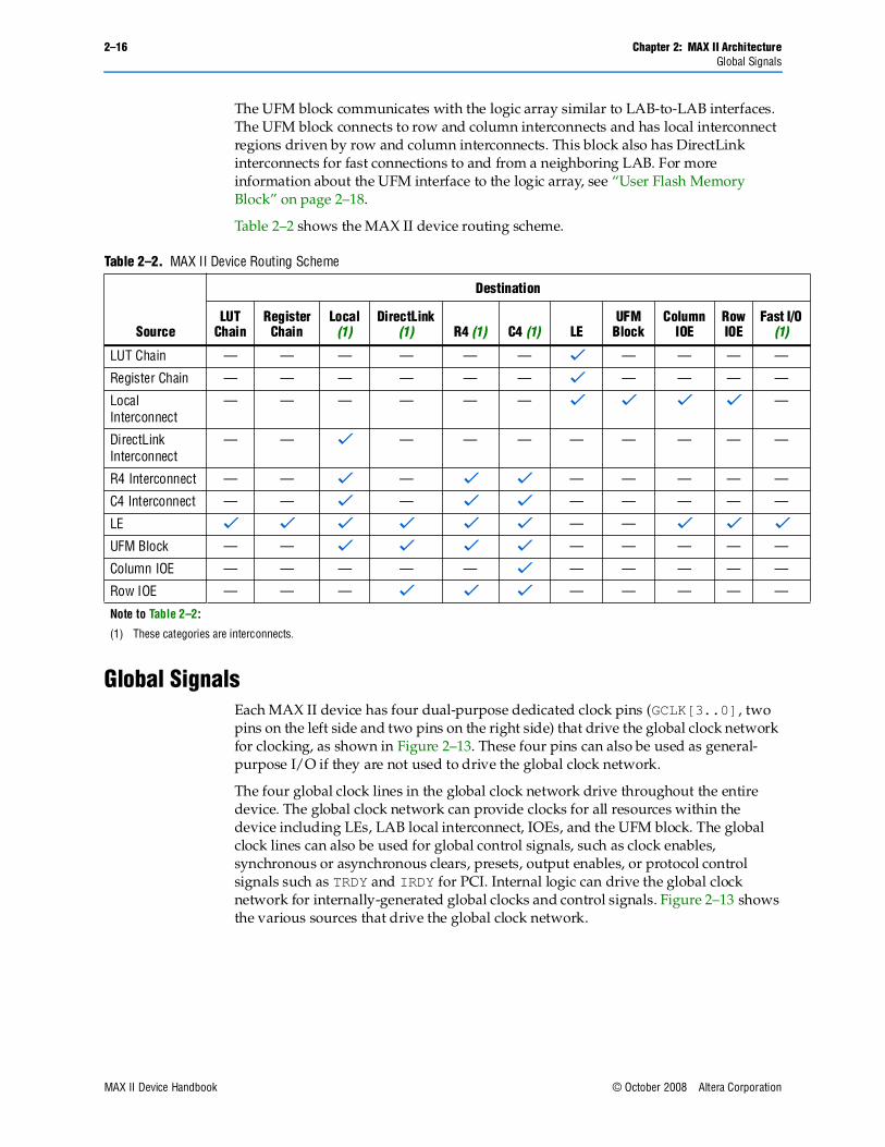
Table 2–2 shows the MAX II device routing scheme.
Global SignalsEach MAX II device has four dual-purpose dedicated clock pins (GCLK[3..0], two pins on the left side and two pins on the right side) that drive the global clock network for clocking, as shown in Figure 2–13. These four pins can also be used as general-purpose I/O if they are not used to drive the global clock network.
The four global clock lines in the global clock network drive throughout the entire device. The global clock network can provide clocks for all resources within the device including LEs, LAB local interconnect, IOEs, and the UFM block. The global clock lines can also be used for global control signals, such as clock enables, synchronous or asynchronous clears, presets, output enables, or protocol control signals such as TRDY and IRDY for PCI. Internal logic can drive the global clock network for internally-generated global clocks and control signals. Figure 2–13 shows the various sources that drive the global clock network.
Table 2–2. MAX II Device Routing Scheme
Source
Destination
LUT Chain
Register Chain
Local (1)
DirectLink (1) R4 (1) C4 (1) LE
UFM Block
Column IOE
Row IOE
Fast I/O(1)
LUT Chain — — — — — — v — — — —
Register Chain — — — — — — v — — — —
Local Interconnect
— — — — — — v v v v —
DirectLink Interconnect
— — v — — — — — — — —
R4 Interconnect — — v — v v — — — — —
C4 Interconnect — — v — v v — — — — —
LE v v v v v v — — v v vUFM Block — — v v v v — — — — —
Column IOE — — — — — v — — — — —
Row IOE — — — v v v — — — — —
Note to Table 2–2:
(1) These categories are interconnects.
MAX II Device Handbook © October 2008 Altera Corporation

Chapter 2: MAX II Architecture 2–17Global Signals
The global clock network drives to individual LAB column signals, LAB column clocks [3..0], that span an entire LAB column from the top to the bottom of the device. Unused global clocks or control signals in a LAB column are turned off at the LAB column clock buffers shown in Figure 2–14. The LAB column clocks [3..0] are multiplexed down to two LAB clock signals and one LAB clear signal. Other control signal types route from the global clock network into the LAB local interconnect. See “LAB Control Signals” on page 2–5 for more information.
Figure 2–13. Global Clock Generation
Note to Figure 2–13:(1) Any I/O pin can use a MultiTrack interconnect to route as a logic array-generated global clock signal.
4
4
GCLK0
Global ClockNetwork
GCLK1GCLK2GCLK3
Logic Array(1)
© October 2008 Altera Corporation MAX II Device Handbook

2–18 Chapter 2: MAX II ArchitectureUser Flash Memory Block
User Flash Memory BlockMAX II devices feature a single UFM block, which can be used like a serial EEPROM for storing non-volatile information up to 8,192 bits. The UFM block connects to the logic array through the MultiTrack interconnect, allowing any LE to interface to the UFM block. Figure 2–15 shows the UFM block and interface signals. The logic array is used to create customer interface or protocol logic to interface the UFM block data outside of the device. The UFM block offers the following features:
■ Non-volatile storage up to 16-bit wide and 8,192 total bits
■ Two sectors for partitioned sector erase
■ Built-in internal oscillator that optionally drives logic array
■ Program, erase, and busy signals
Figure 2–14. Global Clock Network (Note 1)
Notes to Figure 2–14:(1) LAB column clocks in I/O block regions provide high fan-out output enable signals.(2) LAB column clocks drive to the UFM block.
UFM Block (2)
CFM Block
I/O Block Region
I/O Block Region
I/O Block Region
LAB Column clock[3..0]
LAB Columnclock[3..0]
4 4 4 4 4 4 4 4
MAX II Device Handbook © October 2008 Altera Corporation

Chapter 2: MAX II Architecture 2–19User Flash Memory Block
■ Auto-increment addressing
■ Serial interface to logic array with programmable interface
UFM StorageEach device stores up to 8,192 bits of data in the UFM block. Table 2–3 shows the data size, sector, and address sizes for the UFM block.
There are 512 locations with 9-bit addressing ranging from 000h to 1FFh. Sector 0 address space is 000h to 0FFh and Sector 1 address space is from 100h to 1FFh. The data width is up to 16 bits of data. The Quartus II software automatically creates logic to accommodate smaller read or program data widths. Erasure of the UFM involves individual sector erasing (that is, one erase of sector 0 and one erase of sector 1 is required to erase the entire UFM block). Since sector erase is required before a program or write, having two sectors enables a sector size of data to be left untouched while the other sector is erased and programmed with new data.
Figure 2–15. UFM Block and Interface Signals
OSC 4
ProgramErase
Control
UFM Sector 1
UFM Sector 0
:_
AddressRegister
PROGRAM
ERASE
OSC_ENA
RTP_BUSY
BUSY
OSC
Data Register
UFM Block
DRDin DRDout
ARCLK
ARSHFT
ARDin
DRCLK
DRSHFT
16 16
9
Table 2–3. UFM Array Size
Device Total Bits Sectors Address Bits Data Width
EPM240
EPM570
EPM1270
EPM2210
8,192 2 (4,096 bits/sector)
9 16
© October 2008 Altera Corporation MAX II Device Handbook

2–20 Chapter 2: MAX II ArchitectureUser Flash Memory Block
Internal OscillatorAs shown in Figure 2–15, the dedicated circuitry within the UFM block contains an oscillator. The dedicated circuitry uses this internally for its read and program operations. This oscillator's divide by 4 output can drive out of the UFM block as a logic interface clock source or for general-purpose logic clocking. The typical OSC output signal frequency ranges from 3.3 to 5.5 MHz, and its exact frequency of operation is not programmable.
Program, Erase, and Busy SignalsThe UFM block’s dedicated circuitry automatically generates the necessary internal program and erase algorithm once the PROGRAM or ERASE input signals have been asserted. The PROGRAM or ERASE signal must be asserted until the busy signal deasserts, indicating the UFM internal program or erase operation has completed. The UFM block also supports JTAG as the interface for programming and/or reading.
f For more information about programming and erasing the UFM block, refer to the Using User Flash Memory in MAX II Devices chapter in the MAX II Device Handbook.
Auto-Increment AddressingThe UFM block supports standard read or stream read operations. The stream read is supported with an auto-increment address feature. Deasserting the ARSHIFT signal while clocking the ARCLK signal increments the address register value to read consecutive locations from the UFM array.
Serial InterfaceThe UFM block supports a serial interface with serial address and data signals. The internal shift registers within the UFM block for address and data are 9 bits and 16 bits wide, respectively. The Quartus II software automatically generates interface logic in LEs for a parallel address and data interface to the UFM block. Other standard protocol interfaces such as SPI are also automatically generated in LE logic by the Quartus II software.
f For more information about the UFM interface signals and the Quartus II LE-based alternate interfaces, refer to the Using User Flash Memory in MAX II Devices chapter in the MAX II Device Handbook.
UFM Block to Logic Array InterfaceThe UFM block is a small partition of the flash memory that contains the CFM block, as shown in Figure 2–1 and Figure 2–2. The UFM block for the EPM240 device is located on the left side of the device adjacent to the left most LAB column. The UFM block for the EPM570, EPM1270, and EPM2210 devices is located at the bottom left of the device. The UFM input and output signals interface to all types of interconnects (R4 interconnect, C4 interconnect, and DirectLink interconnect to/from adjacent LAB rows). The UFM signals can also be driven from global clocks, GCLK[3..0]. The interface region for the EPM240 device is shown in Figure 2–16. The interface regions for EPM570, EPM1270, and EPM2210 devices are shown in Figure 2–17.
MAX II Device Handbook © October 2008 Altera Corporation

Chapter 2: MAX II Architecture 2–21User Flash Memory Block
Figure 2–16. EPM240 UFM Block LAB Row Interface (Note 1)
Note to Figure 2–16:
(1) The UFM block inputs and outputs can drive to/from all types of interconnects, not only DirectLink interconnects from adjacent row LABs.
UFM Block
CFM Block
PROGRAM
ERASE
OSC_ENA
DRDinDRCLK
DRSHFTARin
ARCLKARSHFTDRDout
OSCBUSY
RTP_BUSY
LAB
LAB
LAB
© October 2008 Altera Corporation MAX II Device Handbook

2–22 Chapter 2: MAX II ArchitectureMultiVolt Core
MultiVolt CoreThe MAX II architecture supports the MultiVolt core feature, which allows MAX II devices to support multiple VCC levels on the VCCINT supply. An internal linear voltage regulator provides the necessary 1.8-V internal voltage supply to the device. The voltage regulator supports 3.3-V or 2.5-V supplies on its inputs to supply the 1.8-V internal voltage to the device, as shown in Figure 2–18. The voltage regulator is not guaranteed for voltages that are between the maximum recommended 2.5-V operating voltage and the minimum recommended 3.3-V operating voltage.
The MAX IIG and MAX IIZ devices use external 1.8-V supply. The 1.8-V VCC external supply powers the device core directly.
Figure 2–17. EPM570, EPM1270, and EPM2210 UFM Block LAB Row Interface
RTP_BUSYBUSY
OSCDRDout
DRDin
PROGRAMERASE
OSC_ENAARCLK
ARSHFT
DRDCLKDRDSHFT
ARDin
UFM Block
CFM Block
LAB
LAB
LAB
Figure 2–18. MultiVolt Core Feature in MAX II Devices
MAX II Device
3.3-V or 2.5-V onVCCINT Pins
VoltageRegulator
1.8-V CoreVoltage
MAX IIG or MAX IIZ Device
1.8-V onVCCINT Pins
1.8-V CoreVoltage
MAX II Device Handbook © October 2008 Altera Corporation

Chapter 2: MAX II Architecture 2–23I/O Structure
I/O StructureIOEs support many features, including:
■ LVTTL and LVCMOS I/O standards
■ 3.3-V, 32-bit, 66-MHz PCI compliance
■ Joint Test Action Group (JTAG) boundary-scan test (BST) support
■ Programmable drive strength control
■ Weak pull-up resistors during power-up and in system programming
■ Slew-rate control
■ Tri-state buffers with individual output enable control
■ Bus-hold circuitry
■ Programmable pull-up resistors in user mode
■ Unique output enable per pin
■ Open-drain outputs
■ Schmitt trigger inputs
■ Fast I/O connection
■ Programmable input delay
MAX II device IOEs contain a bidirectional I/O buffer. Figure 2–19 shows the MAX II IOE structure. Registers from adjacent LABs can drive to or be driven from the IOE’s bidirectional I/O buffers. The Quartus II software automatically attempts to place registers in the adjacent LAB with fast I/O connection to achieve the fastest possible clock-to-output and registered output enable timing. For input registers, the Quartus II software automatically routes the register to guarantee zero hold time. You can set timing assignments in the Quartus II software to achieve desired I/O timing.
Fast I/O ConnectionA dedicated fast I/O connection from the adjacent LAB to the IOEs within an I/O block provides faster output delays for clock-to-output and tPD propagation delays. This connection exists for data output signals, not output enable signals or input signals. Figure 2–20, Figure 2–21, and Figure 2–22 illustrate the fast I/O connection.
© October 2008 Altera Corporation MAX II Device Handbook

2–24 Chapter 2: MAX II ArchitectureI/O Structure
I/O BlocksThe IOEs are located in I/O blocks around the periphery of the MAX II device. There are up to seven IOEs per row I/O block (5 maximum in the EPM240 device) and up to four IOEs per column I/O block. Each column or row I/O block interfaces with its adjacent LAB and MultiTrack interconnect to distribute signals throughout the device. The row I/O blocks drive row, column, or DirectLink interconnects. The column I/O blocks drive column interconnects.
Figure 2–19. MAX II IOE Structure
Note to Figure 2–19:(1) Available in EPM1270 and EPM2210 devices only.
Data_in
Optional SchmittTrigger Input
Drive Strength ControlOpen-Drain Output
Slew Control
Fast_out
Data_out OE
OptionalPCI Clamp (1)
ProgrammablePull-Up
VCCIO VCCIO
I/O Pin
Optional Bus-Hold Circuit
DEV_OE
ProgrammableInput Delay
MAX II Device Handbook © October 2008 Altera Corporation

Chapter 2: MAX II Architecture 2–25I/O Structure
Figure 2–20 shows how a row I/O block connects to the logic array.
Figure 2–20. Row I/O Block Connection to the Interconnect (Note 1)
Note to Figure 2–20:(1) Each of the seven IOEs in the row I/O block can have one data_out or fast_out output, one OE output, and one data_in input.
7
R4 Interconnects C4 Interconnects
I/O Block Local Interconnect
data_in[6..0]
data_out[6..0]
7
OE[6..0]
7
7
fast_out[6..0]
Row I/O BlockContains up to
Seven IOEs
Direct LinkInterconnect
to Adjacent LAB
Direct LinkInterconnect
from Adjacent LAB
LAB Columnclock [3..0]
LAB LocalInterconnect
LAB RowI/O Block
© October 2008 Altera Corporation MAX II Device Handbook

2–26 Chapter 2: MAX II ArchitectureI/O Structure
Figure 2–21 shows how a column I/O block connects to the logic array.
I/O Standards and BanksMAX II device IOEs support the following I/O standards:
■ 3.3-V LVTTL/LVCMOS
■ 2.5-V LVTTL/LVCMOS
■ 1.8-V LVTTL/LVCMOS
■ 1.5-V LVCMOS
■ 3.3-V PCI
Figure 2–21. Column I/O Block Connection to the Interconnect (Note 1)
Note to Figure 2–21:(1) Each of the four IOEs in the column I/O block can have one data_out or fast_out output, one OE output, and one data_in input.
Column I/O Block ContainsUp To 4 IOEs
I/O BlockLocal Interconnect
R4 Interconnects
LAB LocalInterconnect
C4 Interconnects
LAB LocalInterconnect
C4 Interconnects
4
LAB LAB LAB
data_out[3..0]
4
OE[3..0]
4
fast_out[3..0]
Fast I/OInterconnect
Path
4
data_in[3..0]
Column I/O Block
LAB LocalInterconnect
LAB ColumnClock [3..0]
MAX II Device Handbook © October 2008 Altera Corporation

Chapter 2: MAX II Architecture 2–27I/O Structure
Table 2–4 describes the I/O standards supported by MAX II devices.
The EPM240 and EPM570 devices support two I/O banks, as shown in Figure 2–22. Each of these banks support all the LVTTL and LVCMOS standards shown in Table 2–4. PCI compliant I/O is not supported in these devices and banks.
The EPM1270 and EPM2210 devices support four I/O banks, as shown in Figure 2–23. Each of these banks support all of the LVTTL and LVCMOS standards shown in Table 2–4. PCI compliant I/O is supported in Bank 3. Bank 3 supports the PCI clamping diode on inputs and PCI drive compliance on outputs. You must use Bank 3 for designs requiring PCI compliant I/O pins. The Quartus II software automatically places I/O pins in this bank if assigned with the PCI I/O standard.
Table 2–4. MAX II I/O Standards
I/O Standard TypeOutput Supply Voltage
(VCCIO) (V)
3.3-V LVTTL/LVCMOS Single-ended 3.3
2.5-V LVTTL/LVCMOS Single-ended 2.5
1.8-V LVTTL/LVCMOS Single-ended 1.8
1.5-V LVCMOS Single-ended 1.5
3.3-V PCI (1) Single-ended 3.3
Note to Table 2–4:
(1) The 3.3-V PCI compliant I/O is supported in Bank 3 of the EPM1270 and EPM2210 devices.
Figure 2–22. MAX II I/O Banks for EPM240 and EPM570 (Note 1), (2)
Notes to Figure 2–22:(1) Figure 2–22 is a top view of the silicon die.
(2) Figure 2–22 is a graphical representation only. Refer to the pin list and the Quartus II software for exact pin locations.
All I/O Banks Support■ 3.3-V LVTTL/LVCMOS ■ 2.5-V LVTTL/LVCMOS■ 1.8-V LVTTL/LVCMOS■ 1.5-V LVCMOS
I/O Bank 2I/O Bank 1
© October 2008 Altera Corporation MAX II Device Handbook

2–28 Chapter 2: MAX II ArchitectureI/O Structure
Each I/O bank has dedicated VCCIO pins that determine the voltage standard support in that bank. A single device can support 1.5-V, 1.8-V, 2.5-V, and 3.3-V interfaces; each individual bank can support a different standard. Each I/O bank can support multiple standards with the same VCCIO for input and output pins. For example, when VCCIO is 3.3 V, Bank 3 can support LVTTL, LVCMOS, and 3.3-V PCI. VCCIO powers both the input and output buffers in MAX II devices.
The JTAG pins for MAX II devices are dedicated pins that cannot be used as regular I/O pins. The pins TMS, TDI, TDO, and TCK support all the I/O standards shown in Table 2–4 on page 2–27 except for PCI. These pins reside in Bank 1 for all MAX II devices and their I/O standard support is controlled by the VCCIO setting for Bank 1.
PCI ComplianceThe MAX II EPM1270 and EPM2210 devices are compliant with PCI applications as well as all 3.3-V electrical specifications in the PCI Local Bus Specification Revision 2.2. These devices are also large enough to support PCI intellectual property (IP) cores. Table 2–5 shows the MAX II device speed grades that meet the PCI timing specifications.
Figure 2–23. MAX II I/O Banks for EPM1270 and EPM2210 (Note 1), (2)
Notes to Figure 2–23:
(1) Figure 2–23 is a top view of the silicon die.(2) Figure 2–23 is a graphical representation only. Refer to the pin list and the Quartus II software for exact pin locations.
I/O Bank 2
I/O Bank 3
I/O Bank 4
I/O Bank 1
All I/O Banks Support■ 3.3-V LVTTL/LVCMOS ■ 2.5-V LVTTL/LVCMOS■ 1.8-V LVTTL/LVCMOS■ 1.5-V LVCMOS
Also Supportsthe 3.3-V PCII/O Standard
MAX II Device Handbook © October 2008 Altera Corporation

Chapter 2: MAX II Architecture 2–29I/O Structure
Schmitt TriggerThe input buffer for each MAX II device I/O pin has an optional Schmitt trigger setting for the 3.3-V and 2.5-V standards. The Schmitt trigger allows input buffers to respond to slow input edge rates with a fast output edge rate. Most importantly, Schmitt triggers provide hysteresis on the input buffer, preventing slow-rising noisy input signals from ringing or oscillating on the input signal driven into the logic array. This provides system noise tolerance on MAX II inputs, but adds a small, nominal input delay.
The JTAG input pins (TMS, TCK, and TDI) have Schmitt trigger buffers that are always enabled.
1 The TCK input is susceptible to high pulse glitches when the input signal fall time is greater than 200 ns for all I/O standards.
Output Enable SignalsEach MAX II IOE output buffer supports output enable signals for tri-state control. The output enable signal can originate from the GCLK[3..0] global signals or from the MultiTrack interconnect. The MultiTrack interconnect routes output enable signals and allows for a unique output enable for each output or bidirectional pin.
MAX II devices also provide a chip-wide output enable pin (DEV_OE) to control the output enable for every output pin in the design. An option set before compilation in the Quartus II software controls this pin. This chip-wide output enable uses its own routing resources and does not use any of the four global resources. If this option is turned on, all outputs on the chip operate normally when DEV_OE is asserted. When the pin is deasserted, all outputs are tri-stated. If this option is turned off, the DEV_OE pin is disabled when the device operates in user mode and is available as a user I/O pin.
Programmable Drive StrengthThe output buffer for each MAX II device I/O pin has two levels of programmable drive strength control for each of the LVTTL and LVCMOS I/O standards. Programmable drive strength provides system noise reduction control for high performance I/O designs. Although a separate slew-rate control feature exists, using the lower drive strength setting provides signal slew-rate control to reduce system noise and signal overshoot without the large delay adder associated with the slew-rate control feature. Table 2–6 shows the possible settings for the I/O standards with drive strength control. The Quartus II software uses the maximum current strength as the default setting. The PCI I/O standard is always set at 20 mA with no alternate setting.
Table 2–5. MAX II Devices and Speed Grades that Support 3.3-V PCI Electrical Specifications and Meet PCI Timing
Device 33-MHz PCI 66-MHz PCI
EPM1270 All Speed Grades –3 Speed Grade
EPM2210 All Speed Grades –3 Speed Grade
© October 2008 Altera Corporation MAX II Device Handbook

2–30 Chapter 2: MAX II ArchitectureI/O Structure
Slew-Rate ControlThe output buffer for each MAX II device I/O pin has a programmable output slew-rate control that can be configured for low noise or high-speed performance. A faster slew rate provides high-speed transitions for high-performance systems. However, these fast transitions may introduce noise transients into the system. A slow slew rate reduces system noise, but adds a nominal output delay to rising and falling edges. The lower the voltage standard (for example, 1.8-V LVTTL) the larger the output delay when slow slew is enabled. Each I/O pin has an individual slew-rate control, allowing the designer to specify the slew rate on a pin-by-pin basis. The slew-rate control affects both the rising and falling edges.
Open-Drain OutputMAX II devices provide an optional open-drain (equivalent to open-collector) output for each I/O pin. This open-drain output enables the device to provide system-level control signals (for example, interrupt and write enable signals) that can be asserted by any of several devices. This output can also provide an additional wired-OR plane.
Programmable Ground PinsEach unused I/O pin on MAX II devices can be used as an additional ground pin. This programmable ground feature does not require the use of the associated LEs in the device. In the Quartus II software, unused pins can be set as programmable GND on a global default basis or they can be individually assigned. Unused pins also have the option of being set as tri-stated input pins.
Table 2–6. Programmable Drive Strength (Note 1)
I/O Standard IOH/IOL Current Strength Setting (mA)
3.3-V LVTTL 16
8
3.3-V LVCMOS 8
4
2.5-V LVTTL/LVCMOS 14
7
1.8-V LVTTL/LVCMOS 6
3
1.5-V LVCMOS 4
2
Note to Table 2–6:
(1) The IOH current strength numbers shown are for a condition of a VOUT = VOH minimum, where the VOH minimum is specified by the I/O standard. The IOL current strength numbers shown are for a condition of a VOUT = VOL maximum, where the VOL maximum is specified by the I/O standard. For 2.5-V LVTTL/LVCMOS, the IOH condition is VOUT = 1.7 V and the IOL condition is VOUT = 0.7 V.
MAX II Device Handbook © October 2008 Altera Corporation

Chapter 2: MAX II Architecture 2–31I/O Structure
Bus HoldEach MAX II device I/O pin provides an optional bus-hold feature. The bus-hold circuitry can hold the signal on an I/O pin at its last-driven state. Since the bus-hold feature holds the last-driven state of the pin until the next input signal is present, an external pull-up or pull-down resistor is not necessary to hold a signal level when the bus is tri-stated.
The bus-hold circuitry also pulls undriven pins away from the input threshold voltage where noise can cause unintended high-frequency switching. The designer can select this feature individually for each I/O pin. The bus-hold output will drive no higher than VCCIO to prevent overdriving signals. If the bus-hold feature is enabled, the device cannot use the programmable pull-up option.
The bus-hold circuitry uses a resistor to pull the signal level to the last driven state. The DC and Switching Characteristics chapter in the MAX II Device Handbook gives the specific sustaining current for each VCCIO voltage level driven through this resistor and overdrive current used to identify the next-driven input level.
The bus-hold circuitry is only active after the device has fully initialized. The bus-hold circuit captures the value on the pin present at the moment user mode is entered.
Programmable Pull-Up ResistorEach MAX II device I/O pin provides an optional programmable pull-up resistor during user mode. If the designer enables this feature for an I/O pin, the pull-up resistor holds the output to the VCCIO level of the output pin’s bank.
1 The programmable pull-up resistor feature should not be used at the same time as the bus-hold feature on a given I/O pin.
Programmable Input DelayThe MAX II IOE includes a programmable input delay that is activated to ensure zero hold times. A path where a pin directly drives a register, with minimal routing between the two, may require the delay to ensure zero hold time. However, a path where a pin drives a register through long routing or through combinational logic may not require the delay to achieve a zero hold time. The Quartus II software uses this delay to ensure zero hold times when needed.
MultiVolt I/O InterfaceThe MAX II architecture supports the MultiVolt I/O interface feature, which allows MAX II devices in all packages to interface with systems of different supply voltages. The devices have one set of VCC pins for internal operation (VCCINT), and up to four sets for input buffers and I/O output driver buffers (VCCIO), depending on the number of I/O banks available in the devices where each set of VCC pins powers one I/O bank. The EPM240 and EPM570 devices have two I/O banks respectively while the EPM1270 and EPM2210 devices have four I/O banks respectively.
© October 2008 Altera Corporation MAX II Device Handbook
2–32 Chapter 2: MAX II ArchitectureReferenced Documents
Connect VCCIO pins to either a 1.5-V, 1.8 V, 2.5-V, or 3.3-V power supply, depending on the output requirements. The output levels are compatible with systems of the same voltage as the power supply (that is, when VCCIO pins are connected to a 1.5-V power supply, the output levels are compatible with 1.5-V systems). When VCCIO pins are connected to a 3.3-V power supply, the output high is 3.3 V and is compatible with 3.3-V or 5.0-V systems. Table 2–7 summarizes MAX II MultiVolt I/O support.
f For information about output pin source and sink current guidelines, refer to the AN 428: MAX II CPLD Design Guidelines.
Referenced DocumentsThis chapter referenced the following documents:
■ AN 428: MAX II CPLD Design Guidelines
■ DC and Switching Characteristics chapter in the MAX II Device Handbook
■ Hot Socketing and Power-On Reset in MAX II Devices chapter in the MAX II Device Handbook
■ Using User Flash Memory in MAX II Devices chapter in the MAX II Device Handbook
Table 2–7. MAX II MultiVolt I/O Support (Note 1)
VCCIO (V)
Input Signal Output Signal
1.5 V 1.8 V 2.5 V 3.3 V 5.0 V 1.5 V 1.8 V 2.5 V 3.3 V 5.0 V
1.5 v v v v — v — — — —
1.8 v v v v — v (2) v — — —
2.5 — — v v — v (3) v (3) v — —
3.3 — — v (4) v v (5) v (6) v (6) v (6) v v (7)
Notes to Table 2–7:
(1) To drive inputs higher than VCCIO but less than 4.0 V including the overshoot, disable the I/O clamp diode. However, to drive 5.0-V inputs to the device, enable the I/O clamp diode to prevent VI from rising above 4.0 V.
(2) When VCCIO = 1.8 V, a MAX II device can drive a 1.5-V device with 1.8-V tolerant inputs.(3) When VCCIO = 2.5 V, a MAX II device can drive a 1.5-V or 1.8-V device with 2.5-V tolerant inputs.(4) When VCCIO = 3.3 V and a 2.5-V input signal feeds an input pin, the VCCIO supply current will be slightly larger than expected.(5) MAX II devices can be 5.0-V tolerant with the use of an external resistor and the internal I/O clamp diode on the EPM1270 and EPM2210
devices.(6) When VCCIO = 3.3 V, a MAX II device can drive a 1.5-V, 1.8-V, or 2.5-V device with 3.3-V tolerant inputs.(7) When VCCIO = 3.3 V, a MAX II device can drive a device with 5.0-V TTL inputs but not 5.0-V CMOS inputs. In the case of 5.0-V CMOS, open-
drain setting with internal I/O clamp diode (available only on EPM1270 and EPM2210 devices) and external resistor is required.
MAX II Device Handbook © October 2008 Altera Corporation

Chapter 2: MAX II Architecture 2–33Document Revision History
Document Revision HistoryTable 2–8 shows the revision history for this chapter.
Table 2–8. Document Revision History
Date and Revision Changes Made Summary of Changes
October 2008,version 2.2
■ Updated Table 2–4 and Table 2–6.
■ Updated “I/O Standards and Banks” section.
■ Updated New Document Format.
—
March 2008, version 2.1
■ Updated “Schmitt Trigger” section. —
December 2007, version 2.0
■ Updated “Clear and Preset Logic Control” section.
■ Updated “MultiVolt Core” section.
■ Updated “MultiVolt I/O Interface” section.
■ Updated Table 2–7.
■ Added “Referenced Documents” section.
Updated document with MAX IIZ information.
December 2006, version 1.7
■ Minor update in “Internal Oscillator” section. Added document revision history.
—
August 2006,version 1.6
■ Updated functional description and I/O structure sections. —
July 2006,vervion 1.5
■ Minor content and table updates. —
February 2006,version 1.4
■ Updated “LAB Control Signals” section.
■ Updated “Clear and Preset Logic Control” section.
■ Updated “Internal Oscillator” section.
■ Updated Table 2–5.
—
August 2005, version 1.3
■ Removed Note 2 from Table 2-7. —
December 2004, version 1.2
■ Added a paragraph to page 2-15. —
June 2004, version 1.1
■ Added CFM acronym. Corrected Figure 2-19. —
© October 2008 Altera Corporation MAX II Device Handbook

2–34 Chapter 2: MAX II ArchitectureDocument Revision History
MAX II Device Handbook © October 2008 Altera Corporation

© October 2008 Altera Corporation
MII51003-1.6
3. JTAG and In-System Programmability
IntroductionThis chapter discusses how to use the IEEE Standard 1149.1 Boundary-Scan Test (BST) circuitry in MAX II devices and includes the following sections:
■ “IEEE Std. 1149.1 (JTAG) Boundary-Scan Support” on page 3–1
■ “In System Programmability” on page 3–4
IEEE Std. 1149.1 (JTAG) Boundary-Scan SupportAll MAX® II devices provide Joint Test Action Group (JTAG) boundary-scan test (BST) circuitry that complies with the IEEE Std. 1149.1-2001 specification. JTAG boundary-scan testing can only be performed at any time after VCCINT and all VCCIO banks have been fully powered and a tCONFIG amount of time has passed. MAX II devices can also use the JTAG port for in-system programming together with either the Quartus® II software or hardware using Programming Object Files (.pof), JamTM Standard Test and Programming Language (STAPL) Files (.jam), or Jam Byte-Code Files (.jbc).
The JTAG pins support 1.5-V, 1.8-V, 2.5-V, or 3.3-V I/O standards. The supported voltage level and standard are determined by the VCCIO of the bank where it resides. The dedicated JTAG pins reside in Bank 1 of all MAX II devices.
MAX II devices support the JTAG instructions shown in Table 3–1.
Table 3–1. MAX II JTAG Instructions (Part 1 of 2)
JTAG Instruction Instruction Code Description
SAMPLE/PRELOAD 00 0000 0101 Allows a snapshot of signals at the device pins to be captured and examined during normal device operation, and permits an initial data pattern to be output at the device pins.
EXTEST (1) 00 0000 1111 Allows the external circuitry and board-level interconnects to be tested by forcing a test pattern at the output pins and capturing test results at the input pins.
BYPASS 11 1111 1111 Places the 1-bit bypass register between the TDI and TDO pins, which allows the BST data to pass synchronously through selected devices to adjacent devices during normal device operation.
USERCODE 00 0000 0111 Selects the 32-bit USERCODE register and places it between the TDI and TDO pins, allowing the USERCODE to be serially shifted out of TDO. This register defaults to all 1’s if not specified in the Quartus II software.
IDCODE 00 0000 0110 Selects the IDCODE register and places it between TDI and TDO, allowing the IDCODE to be serially shifted out of TDO.
HIGHZ (1) 00 0000 1011 Places the 1-bit bypass register between the TDI and TDO pins, which allows the boundary scan test data to pass synchronously through selected devices to adjacent devices during normal device operation, while tri-stating all of the I/O pins.
MAX II Device Handbook

3–2 Chapter 3: JTAG and In-System ProgrammabilityIEEE Std. 1149.1 (JTAG) Boundary-Scan Support
w Unsupported JTAG instructions should not be issued to the MAX II device as this may put the device into an unknown state, requiring a power cycle to recover device operation.
The MAX II device instruction register length is 10 bits and the USERCODE register length is 32 bits. Table 3–2 and Table 3–3 show the boundary-scan register length and device IDCODE information for MAX II devices.
CLAMP (1) 00 0000 1010 Places the 1-bit bypass register between the TDI and TDO pins, which allows the boundary scan test data to pass synchronously through selected devices to adjacent devices during normal device operation, while holding I/O pins to a state defined by the data in the boundary-scan register.
USER0 00 0000 1100 This instruction allows you to define the scan chain between TDI and TDO in the MAX II logic array. This instruction is also used for custom logic and JTAG interfaces.
USER1 00 0000 1110 This instruction allows you to define the scan chain between TDI and TDO in the MAX II logic array. This instruction is also used for custom logic and JTAG interfaces.
IEEE 1532 instructions
(2) IEEE 1532 ISC instructions used when programming a MAX II device via the JTAG port.
Notes to Table 3–1:
(1) HIGHZ, CLAMP, and EXTEST instructions do not disable weak pull-up resistors or bus hold features.(2) These instructions are shown in the 1532 BSDL files, which will be posted on the Altera® website at www.altera.com when they are available.
Table 3–1. MAX II JTAG Instructions (Part 2 of 2)
JTAG Instruction Instruction Code Description
Table 3–2. MAX II Boundary-Scan Register Length
Device Boundary-Scan Register Length
EPM240 240
EPM570 480
EPM1270 636
EPM2210 816
Table 3–3. 32-Bit MAX II Device IDCODE (Part 1 of 2)
Device
Binary IDCODE (32 Bits) (1)
HEX IDCODEVersion (4 Bits) Part Number
Manufacturer Identity (11 Bits)
LSB (1 Bit) (2)
EPM240
EPM240G
0000 0010 0000 1010 0001 000 0110 1110 1 0x020A10DD
EPM570
EPM570G
0000 0010 0000 1010 0010 000 0110 1110 1 0x020A20DD
EPM1270
EPM1270G
0000 0010 0000 1010 0011 000 0110 1110 1 0x020A30DD
EPM2210
EPM2210G
0000 0010 0000 1010 0100 000 0110 1110 1 0x020A40DD
MAX II Device Handbook © October 2008 Altera Corporation

Chapter 3: JTAG and In-System Programmability 3–3IEEE Std. 1149.1 (JTAG) Boundary-Scan Support
f For JTAG AC characteristics, refer to the DC and Switching Characteristics chapter in the MAX II Device Handbook.
f For more information about JTAG BST, refer to the IEEE 1149.1 (JTAG) Boundary-Scan Testing for MAX II Devices chapter in the MAX II Device Handbook.
JTAG BlockThe MAX II JTAG block feature allows you to access the JTAG TAP and state signals when either the USER0 or USER1 instruction is issued to the JTAG TAP. The USER0 and USER1 instructions bring the JTAG boundary-scan chain (TDI) through the user logic instead of the MAX II device’s boundary-scan cells. Each USER instruction allows for one unique user-defined JTAG chain into the logic array.
Parallel Flash LoaderThe JTAG block ability to interface JTAG to non-JTAG devices is ideal for general-purpose flash memory devices (such as Intel- or Fujitsu-based devices) that require programming during in-circuit test. The flash memory devices can be used for FPGA configuration or be part of system memory. In many cases, the MAX II device is already connected to these devices as the configuration control logic between the FPGA and the flash device. Unlike ISP-capable CPLD devices, bulk flash devices do not have JTAG TAP pins or connections. For small flash devices, it is common to use the serial JTAG scan chain of a connected device to program the non-JTAG flash device. This is slow and inefficient in most cases and impractical for large parallel flash devices. Using the MAX II device’s JTAG block as a parallel flash loader, with the Quartus II software, to program and verify flash contents provides a fast and cost-effective means of in-circuit programming during test. Figure 3–1 shows MAX II being used as a parallel flash loader.
EPM240Z 0000 0010 0000 1010 0101 000 0110 1110 1 0x020A50DD
EPM570Z 0000 0010 0000 1010 0110 000 0110 1110 1 0x020A60DD
Notes to Table 3–2:
(1) The most significant bit (MSB) is on the left.(2) The IDCODE’s least significant bit (LSB) is always 1.
Table 3–3. 32-Bit MAX II Device IDCODE (Part 2 of 2)
Device
Binary IDCODE (32 Bits) (1)
HEX IDCODEVersion (4 Bits) Part Number
Manufacturer Identity (11 Bits)
LSB (1 Bit) (2)
© October 2008 Altera Corporation MAX II Device Handbook

3–4 Chapter 3: JTAG and In-System ProgrammabilityIn System Programmability
In System Programmability MAX II devices can be programmed in-system via the industry standard 4-pin IEEE Std. 1149.1 (JTAG) interface. In-system programmability (ISP) offers quick, efficient iterations during design development and debugging cycles. The logic, circuitry, and interconnects in the MAX II architecture are configured with flash-based SRAM configuration elements. These SRAM elements require configuration data to be loaded each time the device is powered. The process of loading the SRAM data is called configuration. The on-chip configuration flash memory (CFM) block stores the SRAM element’s configuration data. The CFM block stores the design’s configuration pattern in a reprogrammable flash array. During ISP, the MAX II JTAG and ISP circuitry programs the design pattern into the CFM block’s non-volatile flash array.
The MAX II JTAG and ISP controller internally generate the high programming voltages required to program the CFM cells, allowing in-system programming with any of the recommended operating external voltage supplies (that is, 3.3 V/2.5 V or 1.8 V for the MAX IIG and MAX IIZ devices). ISP can be performed anytime after VCCINT and all VCCIO banks have been fully powered and the device has completed the configuration power-up time. By default, during in-system programming, the I/O pins are tri-stated and weakly pulled-up to VCCIO to eliminate board conflicts. The in-system programming clamp and real-time ISP feature allow user control of I/O state or behavior during ISP.
For more information, refer to “In-System Programming Clamp” on page 3–6 and “Real-Time ISP” on page 3–7.
These devices also offer an ISP_DONE bit that provides safe operation when in-system programming is interrupted. This ISP_DONE bit, which is the last bit programmed, prevents all I/O pins from driving until the bit is programmed.
Figure 3–1. MAX II Parallel Flash Loader
Notes to Figure 3–1:(1) This block is implemented in LEs.(2) This function is supported in the Quartus II software.
ParallelFlash LoaderConfiguration
Logic
FlashMemory Device
MAX II Device
DQ[7..0]
RY/BY
A[20..0]OEWECE
DQ[7..0]
RY/BY
A[20..0]OEWECE
TDITMSTCK
TDI_UTDO_U
TMS_UTCK_U
SHIFT_UCLKDR_U
UPDATE_URUNIDLE_U
USER1_U
TDO
Altera FPGA
CONF_DONEnSTATUSnCE
DCLK
DATA0nCONFIG
(1), (2)
MAX II Device Handbook © October 2008 Altera Corporation

Chapter 3: JTAG and In-System Programmability 3–5In System Programmability
IEEE 1532 SupportThe JTAG circuitry and ISP instruction set in MAX II devices is compliant to the IEEE 1532-2002 programming specification. This provides industry-standard hardware and software for in-system programming among multiple vendor programmable logic devices (PLDs) in a JTAG chain.
The MAX II 1532 BSDL files will be released on the Altera website when available.
Jam Standard Test and Programming Language (STAPL)The Jam STAPL JEDEC standard, JESD71, can be used to program MAX II devices with in-circuit testers, PCs, or embedded processors. The Jam byte code is also supported for MAX II devices. These software programming protocols provide a compact embedded solution for programming MAX II devices.
f For more information, refer to the Using Jam STAPL for ISP via an Embedded Processor chapter in the MAX II Device Handbook.
Programming SequenceDuring in-system programming, 1532 instructions, addresses, and data are shifted into the MAX II device through the TDI input pin. Data is shifted out through the TDO output pin and compared against the expected data. Programming a pattern into the device requires the following six ISP steps. A stand-alone verification of a programmed pattern involves only stages 1, 2, 5, and 6. These steps are automatically executed by third-party programmers, the Quartus II software, or the Jam STAPL and Jam Byte-Code Players.
1. Enter ISP—The enter ISP stage ensures that the I/O pins transition smoothly from user mode to ISP mode.
2. Check ID—Before any program or verify process, the silicon ID is checked. The time required to read this silicon ID is relatively small compared to the overall programming time.
3. Sector Erase—Erasing the device in-system involves shifting in the instruction to erase the device and applying an erase pulse(s). The erase pulse is automatically generated internally by waiting in the run/test/idle state for the specified erase pulse time of 500 ms for the CFM block and 500 ms for each sector of the UFM block.
4. Program—Programming the device in-system involves shifting in the address, data, and program instruction and generating the program pulse to program the flash cells. The program pulse is automatically generated internally by waiting in the run/test/idle state for the specified program pulse time of 75 µs. This process is repeated for each address in the CFM and UFM blocks.
5. Verify—Verifying a MAX II device in-system involves shifting in addresses, applying the verify instruction to generate the read pulse, and shifting out the data for comparison. This process is repeated for each CFM and UFM address.
6. Exit ISP—An exit ISP stage ensures that the I/O pins transition smoothly from ISP mode to user mode.
© October 2008 Altera Corporation MAX II Device Handbook

3–6 Chapter 3: JTAG and In-System ProgrammabilityIn System Programmability
Table 3–4 shows the programming times for MAX II devices using in-circuit testers to execute the algorithm vectors in hardware. Software-based programming tools used with download cables are slightly slower because of data processing and transfer limitations.
UFM ProgrammingThe Quartus II software, with the use of POF, Jam, or JBC files, supports programming of the user flash memory (UFM) block independent of the logic array design pattern stored in the CFM block. This allows updating or reading UFM contents through ISP without altering the current logic array design, or vice versa. By default, these programming files and methods will program the entire flash memory contents, which includes the CFM block and UFM contents. The stand-alone embedded Jam STAPL player and Jam Byte-Code Player provides action commands for programming or reading the entire flash memory (UFM and CFM together) or each independently.
f For more information, refer to the Using Jam STAPL for ISP via an Embedded Processor chapter in the MAX II Device Handbook.
In-System Programming ClampBy default, the IEEE 1532 instruction used for entering ISP automatically tri-states all I/O pins with weak pull-up resistors for the duration of the ISP sequence. However, some systems may require certain pins on MAX II devices to maintain a specific DC logic level during an in-field update. For these systems, an optional in-system programming clamp instruction exists in MAX II circuitry to control I/O behavior during the ISP sequence. The in-system programming clamp instruction enables the device to sample and sustain the value on an output pin (an input pin would remain tri-stated if sampled) or to explicitly set a logic high, logic low, or tri-state value on any pin. Setting these options is controlled on an individual pin basis using the Quartus II software.
f For more information, refer to the Real-Time ISP and ISP Clamp for MAX II Devices chapter in the MAX II Device Handbook.
Table 3–4. MAX II Device Family Programming Times
Description
EPM240 EPM240GEPM240Z
EPM570 EPM570GEPM570Z
EPM1270 EPM1270G
EPM2210 EPM2210G Unit
Erase + Program (1 MHz) 1.72 2.16 2.90 3.92 sec
Erase + Program (10 MHz) 1.65 1.99 2.58 3.40 sec
Verify (1 MHz) 0.09 0.17 0.30 0.49 sec
Verify (10 MHz) 0.01 0.02 0.03 0.05 sec
Complete Program Cycle (1 MHz) 1.81 2.33 3.20 4.41 sec
Complete Program Cycle (10 MHz) 1.66 2.01 2.61 3.45 sec
MAX II Device Handbook © October 2008 Altera Corporation

Chapter 3: JTAG and In-System Programmability 3–7Referenced Documents
Real-Time ISPFor systems that require more than DC logic level control of I/O pins, the real-time ISP feature allows you to update the CFM block with a new design image while the current design continues to operate in the SRAM logic array and I/O pins. A new programming file is updated into the MAX II device without halting the original design’s operation, saving down-time costs for remote or field upgrades. The updated CFM block configures the new design into the SRAM upon the next power cycle. It is also possible to execute an immediate configuration of the SRAM without a power cycle by using a specific sequence of ISP commands. The configuration of SRAM without a power cycle takes a specific amount of time (tCONFIG). During this time, the I/O pins are tri-stated and weakly pulled-up to VCCIO.
Design SecurityAll MAX II devices contain a programmable security bit that controls access to the data programmed into the CFM block. When this bit is programmed, design programming information, stored in the CFM block, cannot be copied or retrieved. This feature provides a high level of design security because programmed data within flash memory cells is invisible. The security bit that controls this function, as well as all other programmed data, is reset only when the device is erased. The SRAM is also invisible and cannot be accessed regardless of the security bit setting. The UFM block data is not protected by the security bit and is accessible through JTAG or logic array connections.
Programming with External HardwareMAX II devices can be programmed by downloading the information via in-circuit testers, embedded processors, the Altera® ByteblasterMV™, MasterBlaster™, ByteBlaster™ II, and USB-Blaster cables.
BP Microsystems, System General, and other programming hardware manufacturers provide programming support for Altera devices. Check their websites for device support information.
Referenced DocumentsThis chapter references the following documents:
■ DC and Switching Characteristics chapter in the MAX II Device Handbook
■ IEEE 1149.1 (JTAG) Boundary-Scan Testing for MAX II Devices chapter in the MAX II Device Handbook
■ Real-Time ISP and ISP Clamp for MAX II Devices chapter in the MAX II Device Handbook
■ Using Jam STAPL for ISP via an Embedded Processor chapter in the MAX II Device Handbook
© October 2008 Altera Corporation MAX II Device Handbook

3–8 Chapter 3: JTAG and In-System ProgrammabilityDocument Revision History
Document Revision HistoryTable 3–5 shows the revision history for this chapter.
Table 3–5. Document Revision History
Date and Revision Changes Made Summary of Changes
October 2008,version 1.6
■ Updated New Document Format. —
December 2007,version 1.5
■ Added warning note after Table 3–1.
■ Updated Table 3–3 and Table 3–4.
■ Added “Referenced Documents” section.
—
December 2006, version 1.4
■ Added document revision history. —
June 2005,version 1.3
■ Added text and Table 3-4. —
June 2005,version 1.3
■ Updated text on pages 3-5 to 3-8. —
June 2004,version 1.1
■ Corrected Figure 3-1. Added CFM acronym. —
MAX II Device Handbook © October 2008 Altera Corporation

© October 2008 Altera Corporation
MII51004-2.1
4. Hot Socketing and Power-On Reset inMAX II Devices
IntroductionMAX® II devices offer hot socketing, also known as hot plug-in or hot swap, and power sequencing support. Designers can insert or remove a MAX II board in a system during operation without undesirable effects to the system bus. The hot socketing feature removes some of the difficulties designers face when using components on printed circuit boards (PCBs) that contain a mixture of 3.3-, 2.5-, 1.8-, and 1.5-V devices.
The MAX II device hot socketing feature provides:
■ Board or device insertion and removal
■ Support for any power-up sequence
■ Non-intrusive I/O buffers to system buses during hot insertion
This chapter contains the following sections:
■ “MAX II Hot-Socketing Specifications” on page 4–1
■ “Power-On Reset Circuitry” on page 4–5
MAX II Hot-Socketing SpecificationsMAX II devices offer all three of the features required for the hot-socketing capability listed above without any external components or special design requirements. The following are hot-socketing specifications:
■ The device can be driven before and during power-up or power-down without any damage to the device itself.
■ I/O pins remain tri-stated during power-up. The device does not drive out before or during power-up, thereby affecting other buses in operation.
■ Signal pins do not drive the VCCIO or VCCINT power supplies. External input signals to device I/O pins do not power the device VCCIO or VCCINT power supplies via internal paths. This is true if the VCCINT and the VCCIO supplies are held at GND.
1 Altera uses GND as reference for the hot-socketing and I/O buffers circuitry designs. You must connect the GND between boards before connecting the VCCINT and the VCCIO
power supplies to ensure device reliability and compliance to the hot-socketing specifications.
Devices Can Be Driven before Power-UpSignals can be driven into the MAX II device I/O pins and GCLK[3..0] pins before or during power-up or power-down without damaging the device. MAX II devices support any power-up or power-down sequence (VCCIO1, VCCIO2, VCCIO3, VCCIO4, VCCINT), simplifying the system-level design.
MAX II Device Handbook

4–2 Chapter 4: Hot Socketing and Power-On Reset in MAX II DevicesHot Socketing Feature Implementation in MAX II Devices
I/O Pins Remain Tri-Stated during Power-UpA device that does not support hot-socketing may interrupt system operation or cause contention by driving out before or during power-up. In a hot socketing situation, the MAX II device’s output buffers are turned off during system power-up. MAX II devices do not drive out until the device attains proper operating conditions and is fully configured. Refer to “Power-On Reset Circuitry” on page 4–5 for information about turn-on voltages.
Signal Pins Do Not Drive the VCCIO or VCCINT Power SuppliesMAX II devices do not have a current path from I/O pins or GCLK[3..0] pins to the VCCIO or VCCINT pins before or during power-up. A MAX II device may be inserted into (or removed from) a system board that was powered up without damaging or interfering with system-board operation. When hot socketing, MAX II devices may have a minimal effect on the signal integrity of the backplane.
AC and DC SpecificationsYou can power up or power down the VCCIO and VCCINT pins in any sequence. During hot socketing, the I/O pin capacitance is less than 8 pF. MAX II devices meet the following hot socketing specifications:
■ The hot socketing DC specification is: | IIOPIN | < 300 A.
■ The hot socketing AC specification is: | IIOPIN | < 8 mA for 10 ns or less.
1 MAX II devices are immune to latch-up when hot socketing. If the TCK JTAG input pin is driven high during hot socketing, the current on that pin might exceed the specifications above.
IIOPIN is the current at any user I/O pin on the device. The AC specification applies when the device is being powered up or powered down. This specification takes into account the pin capacitance but not board trace and external loading capacitance. Additional capacitance for trace, connector, and loading must be taken into consideration separately. The peak current duration due to power-up transients is 10 ns or less.
The DC specification applies when all VCC supplies to the device are stable in the powered-up or powered-down conditions.
Hot Socketing Feature Implementation in MAX II DevicesThe hot socketing feature turns off (tri-states) the output buffer during the power-up event (either VCCINT or VCCIO supplies) or power-down event. The hot-socket circuit generates an internal HOTSCKT signal when either VCCINT or VCCIO is below the threshold voltage during power-up or power-down. The HOTSCKT signal cuts off the output buffer to make sure that no DC current (except for weak pull-up leaking) leaks through the pin. When VCC ramps up very slowly during power-up, VCC may still be relatively low even after the power-on reset (POR) signal is released and device configuration is complete.
MAX II Device Handbook © October 2008 Altera Corporation

Chapter 4: Hot Socketing and Power-On Reset in MAX II Devices 4–3Hot Socketing Feature Implementation in MAX II Devices
1 Make sure that the VCCINT is within the recommended operating range even though SRAM download has completed.
Each I/O and clock pin has the circuitry shown in Figure 4–1.
The POR circuit monitors VCCINT and VCCIO voltage levels and keeps I/O pins tri-stated until the device has completed its flash memory configuration of the SRAM logic. The weak pull-up resistor (R) from the I/O pin to VCCIO is enabled during download to keep the I/O pins from floating. The 3.3-V tolerance control circuit permits the I/O pins to be driven by 3.3 V before VCCIO and/or VCCINT are powered, and it prevents the I/O pins from driving out when the device is not fully powered or operational. The hot socket circuit prevents I/O pins from internally powering VCCIO and VCCINT when driven by external signals before the device is powered.
f For information about 5.0-V tolerance, refer to the Using MAX II Devices in Multi-Voltage Systems chapter in the MAX II Device Handbook.
Figure 4–2 shows a transistor-level cross section of the MAX II device I/O buffers. This design ensures that the output buffers do not drive when VCCIO is powered before VCCINT or if the I/O pad voltage is higher than VCCIO. This also applies for sudden voltage spikes during hot insertion. The VPAD leakage current charges the 3.3-V tolerant circuit capacitance.
Figure 4–1. Hot Socketing Circuit Block Diagram for MAX II Devices
Output Enable
VCCIO
Hot SocketVoltageTolerance
Control
Power OnReset
Monitor
WeakPull-Up
Resistor
PAD
Input Bufferto Logic Array
© October 2008 Altera Corporation MAX II Device Handbook

4–4 Chapter 4: Hot Socketing and Power-On Reset in MAX II DevicesHot Socketing Feature Implementation in MAX II Devices
The CMOS output drivers in the I/O pins intrinsically provide electrostatic discharge (ESD) protection. There are two cases to consider for ESD voltage strikes: positive voltage zap and negative voltage zap.
A positive ESD voltage zap occurs when a positive voltage is present on an I/O pin due to an ESD charge event. This can cause the N+ (Drain)/ P-Substrate junction of the N-channel drain to break down and the N+ (Drain)/P-Substrate/N+ (Source) intrinsic bipolar transistor turn on to discharge ESD current from I/O pin to GND. The dashed line (see Figure 4–3) shows the ESD current discharge path during a positive ESD zap.
Figure 4–2. Transistor-Level Diagram of MAX II Device I/O Buffers
p - substrate
p+ p+
n - well
n+
VCCIO
n+ n+
p - well
IOE Signal
VPAD
IOE Signal or theLarger of VCCIO or VPAD
The Larger ofVCCIO or VPAD
Ensures 3.3-VTolerance andHot-SocketProtection
Figure 4–3. ESD Protection During Positive Voltage Zap
I/O
I/O
Gate
Gate
Drain
Drain
PMOS
NMOS
Source
Source
GND GND
N+
N+
P-Substrate G
S
D
MAX II Device Handbook © October 2008 Altera Corporation

Chapter 4: Hot Socketing and Power-On Reset in MAX II Devices 4–5Power-On Reset Circuitry
When the I/O pin receives a negative ESD zap at the pin that is less than –0.7 V (0.7 V is the voltage drop across a diode), the intrinsic P-Substrate/N+ drain diode is forward biased. Therefore, the discharge ESD current path is from GND to the I/O pin, as shown in Figure 4–4.
Power-On Reset CircuitryMAX II devices have POR circuits to monitor VCCINT and VCCIO voltage levels during power-up. The POR circuit monitors these voltages, triggering download from the non-volatile configuration flash memory (CFM) block to the SRAM logic, maintaining tri-state of the I/O pins (with weak pull-up resistors enabled) before and during this process. When the MAX II device enters user mode, the POR circuit releases the I/O pins to user functionality. The POR circuit of the MAX II (except MAX IIZ) device continues to monitor the VCCINT voltage level to detect a brown-out condition. The POR circuit of the MAX IIZ device does not monitor the VCCINT voltage level after the device enters into user mode. More details are provided in the following sub-sections.
Figure 4–4. ESD Protection During Negative Voltage Zap
I/O
I/O
Gate
Gate
Drain
Drain
PMOS
NMOS
Source
Source
GND GND
N+
N+
P-Substrate G
S
D
© October 2008 Altera Corporation MAX II Device Handbook

4–6 Chapter 4: Hot Socketing and Power-On Reset in MAX II DevicesPower-On Reset Circuitry
Power-Up CharacteristicsWhen power is applied to a MAX II device, the POR circuit monitors VCCINT and begins SRAM download at an approximate voltage of 1.7 V or 1.55 V for MAX IIG and MAX IIZ devices. From this voltage reference, SRAM download and entry into user mode takes 200 to 450 µs maximum, depending on device density. This period of time is specified as tCONFIG in the power-up timing section of the DC and Switching Characteristics chapter in the MAX II Device Handbook.
Entry into user mode is gated by whether all VCCIO banks are powered with sufficient operating voltage. If VCCINT and VCCIO are powered simultaneously, the device enters user mode within the tCONFIG specifications. If VCCIO is powered more than tCONFIG after VCCINT, the device does not enter user mode until 2 µs after all VCCIO banks are powered.
For MAX II and MAX IIG devices, when in user mode, the POR circuitry continues to monitor the VCCINT (but not VCCIO) voltage level to detect a brown-out condition. If there is a VCCINT voltage sag at or below 1.4 V during user mode, the POR circuit resets the SRAM and tri-states the I/O pins. Once VCCINT rises back to approximately 1.7 V (or 1.55 V for MAX IIG devices), the SRAM download restarts and the device begins to operate after tCONFIG time has passed.
For MAX IIZ devices, the POR circuitry does not monitor the VCCINT and VCCIO voltage levels after the device enters user mode. If there is a VCCINT voltage sag below 1.4 V during user mode, the functionality of the device will not be guaranteed and you must power down the VCCINT to 0 V for a minimum of 10 µs before powering the VCCINT and VCCIO up again. Once VCCINT rises from 0 V back to approximately 1.55 V, the SRAM download restarts and the device begins to operate after tCONFIG time has passed.
Figure 4–5 shows the voltages for POR of MAX II, MAX IIG, and MAX IIZ devices during power-up into user mode and from user mode to power-down or brown-out.
1 All VCCINT and VCCIO pins of all banks must be powered on MAX II devices before entering user mode.
MAX II Device Handbook © October 2008 Altera Corporation
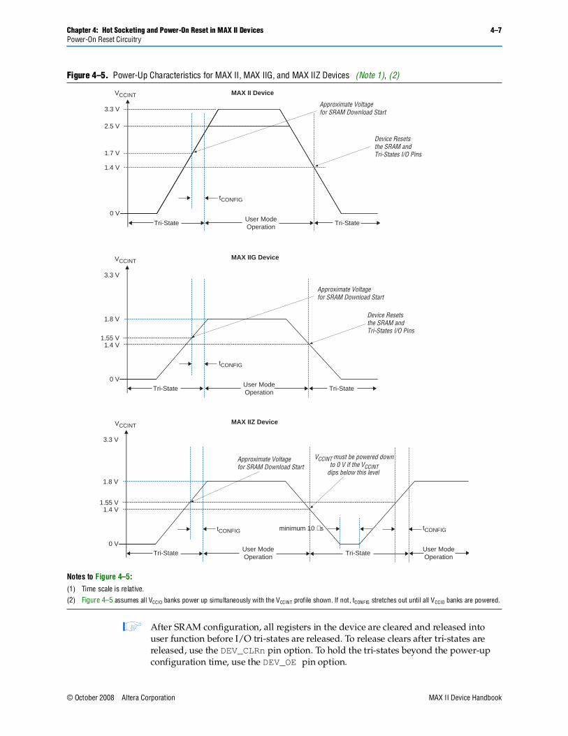
Chapter 4: Hot Socketing and Power-On Reset in MAX II Devices 4–7Power-On Reset Circuitry
1 After SRAM configuration, all registers in the device are cleared and released into user function before I/O tri-states are released. To release clears after tri-states are released, use the DEV_CLRn pin option. To hold the tri-states beyond the power-up configuration time, use the DEV_OE pin option.
Figure 4–5. Power-Up Characteristics for MAX II, MAX IIG, and MAX IIZ Devices (Note 1), (2)
Notes to Figure 4–5:(1) Time scale is relative.(2) Figure 4–5 assumes all VCCIO banks power up simultaneously with the VCCINT profile shown. If not, tCONFIG stretches out until all VCCIO banks are powered.
3.3 V
1.55 V
Tri-StateUser ModeOperation
0 V
1.8 V
Tri-State
1.4 V
3.3 V
0 V
2.5 V
1.7 V
Device Resets the SRAM and Tri-States I/O Pins
Approximate Voltage for SRAM Download Start
MAX II Device
1.4 V
MAX IIG Device
Device Resets the SRAM and Tri-States I/O Pins
Approximate Voltage for SRAM Download Start
3.3 V
1.55 V
Tri-StateUser ModeOperation
0 V
1.8 V
Tri-State
1.4 V
MAX IIZ Device
Approximate Voltage for SRAM Download Start
VCCINT must be powered down to 0 V if the VCCINT dips below this level
tCONFIGtCONFIG
tCONFIG
tCONFIG
User ModeOperation
VCCINT
VCCINT
VCCINT
Tri-StateUser ModeOperation
Tri-State
minimum 10 µs
© October 2008 Altera Corporation MAX II Device Handbook

4–8 Chapter 4: Hot Socketing and Power-On Reset in MAX II DevicesReferenced Documents
Referenced DocumentsThis chapter refereces the following documents:
■ DC and Switching Characteristics chapter in the MAX II Device Handbook
■ Using MAX II Devices in Multi-Voltage Systems chapter in the MAX II Device Handbook
Document Revision HistoryTable 4–1 shows the revision history for this chapter.
Table 4–1. Document Revision History
Date and Revision Changes Made Summary of Changes
October 2008,
version2.1
■ Updated “MAX II Hot-Socketing Specifications” and “Power-On Reset Circuitry” sections.
■ Updated New Document Format.
—
December 2007,version 2.0
■ Updated “Hot Socketing Feature Implementation in MAX II Devices” section.
■ Updated “Power-On Reset Circuitry” section.
■ Updated Figure 4–5.
■ Added “Referenced Documents” section.
Updated document with MAX IIZ information.
December 2006,version 1.5
■ Added document revision history. —
February 2006,version 1.4
■ Updated “MAX II Hot-Socketing Specifications” section.
■ Updated “AC and DC Specifications” section.
■ Updated “Power-On Reset Circuitry” section.
—
June 2005,version 1.3
■ Updated AC and DC specifications on page 4-2. —
December 2004, version 1.2
■ Added content to Power-Up Characteristics section.
■ Updated Figure 4-5.
—
June 2004,version 1.1
■ Corrected Figure 4-2. —
MAX II Device Handbook © October 2008 Altera Corporation

© August 2009 Altera Corporation
MII51005-2.5
5. DC and Switching Characteristics
IntroductionSystem designers must consider the recommended DC and switching conditions discussed in this chapter to maintain the highest possible performance and reliability of the MAX® II devices. This chapter contains the following sections:
■ “Operating Conditions” on page 5–1
■ “Power Consumption” on page 5–8
■ “Timing Model and Specifications” on page 5–8
Operating ConditionsTable 5–1 through Table 5–12 provide information about absolute maximum ratings, recommended operating conditions, DC electrical characteristics, and other specifications for MAX II devices.
Absolute Maximum RatingsTable 5–1 shows the absolute maximum ratings for the MAX II device family.
Table 5–1. MAX II Device Absolute Maximum Ratings (Note 1), (2)
Symbol Parameter Conditions Minimum Maximum Unit
VCCINT Internal supply voltage (3) With respect to ground –0.5 4.6 V
VCCIO I/O supply voltage — –0.5 4.6 V
VI DC input voltage — –0.5 4.6 V
IOUT DC output current, per pin (4) — –25 25 mA
TSTG Storage temperature No bias –65 150 °C
TAMB Ambient temperature Under bias (5) –65 135 °C
TJ Junction temperature TQFP and BGA packages under bias
— 135 °C
Notes to Table 5–1:
(1) Refer to the Operating Requirements for Altera Devices Data Sheet.(2) Conditions beyond those listed in Table 5–1 may cause permanent damage to a device. Additionally, device operation at the absolute maximum
ratings for extended periods of time may have adverse affects on the device.(3) Maximum VCCINT for MAX II devices is 4.6 V. For MAX IIG and MAX IIZ devices, it is 2.4 V.(4) Refer to AN 286: Implementing LED Drivers in MAX & MAX II Devices for more information about the maximum source and sink current for
MAX II devices.(5) Refer to Table 5–2 for information about “under bias” conditions.
MAX II Device Handbook

5–2 Chapter 5: DC and Switching CharacteristicsOperating Conditions
Recommended Operating ConditionsTable 5–2 shows the MAX II device family recommended operating conditions.
Table 5–2. MAX II Device Recommended Operating Conditions
Symbol Parameter Conditions Minimum Maximum Unit
VCCINT (1) 3.3-V supply voltage for internal logic and ISP
MAX II devices 3.00 3.60 V
2.5-V supply voltage for internal logic and ISP
MAX II devices 2.375 2.625 V
1.8-V supply voltage for internal logic and ISP
MAX IIG and MAX IIZ devices
1.71 1.89 V
VCCIO (1) Supply voltage for I/O buffers, 3.3-V operation
— 3.00 3.60 V
Supply voltage for I/O buffers, 2.5-V operation
— 2.375 2.625 V
Supply voltage for I/O buffers, 1.8-V operation
— 1.71 1.89 V
Supply voltage for I/O buffers, 1.5-V operation
— 1.425 1.575 V
VI Input voltage (2), (3), (4) –0.5 4.0 V
VO Output voltage — 0 VCCIO V
TJ Operating junction temperature Commercial range 0 85 °C
Industrial range –40 100 °C
Extended range (5) –40 125 °C
Notes to Table 5–2:
(1) MAX II device in-system programming and/or user flash memory (UFM) programming via JTAG or logic array is not guaranteed outside the recommended operating conditions (for example, if brown-out occurs in the system during a potential write/program sequence to the UFM, users are recommended to read back UFM contents and verify against the intended write data).
(2) Minimum DC input is –0.5 V. During transitions, the inputs may undershoot to –2.0 V for input currents less than 100 mA and periods shorter than 20 ns.
(3) During transitions, the inputs may overshoot to the voltages shown in the following table based upon input duty cycle. The DC case is equivalent to 100% duty cycle. For more information about 5.0-V tolerance, refer to the Using MAX II Devices in Multi-Voltage Systems chapter in the MAX II Device Handbook.VIN Max. Duty Cycle4.0 V 100% (DC)4.1 90%4.2 50%4.3 30%4.4 17%4.5 10%
(4) All pins, including clock, I/O, and JTAG pins, may be driven before VCCINT and VCCIO are powered.(5) For the extended temperature range of 100 to 125º C, MAX II UFM programming (erase/write) is only supported via the JTAG interface. UFM
programming via the logic array interface is not guaranteed in this range.
MAX II Device Handbook © August 2009 Altera Corporation

Chapter 5: DC and Switching Characteristics 5–3Operating Conditions
Programming/Erasure SpecificationsTable 5–3 shows the MAX II device family programming/erasure specifications.
DC Electrical CharacteristicsTable 5–4 shows the MAX II device family DC electrical characteristics.
Table 5–3. MAX II Device Programming/Erasure Specifications
Parameter Minimum Typical Maximum Unit
Erase and reprogram cycles — — 100 (1) Cycles
Note to Table 5–3:
(1) This specification applies to the UFM and configuration flash memory (CFM) blocks.
Table 5–4. MAX II Device DC Electrical Characteristics (Note 1) (Part 1 of 2)
Symbol Parameter Conditions Minimum Typical Maximum Unit
II Input pin leakage current
VI = VCCIOmax to 0 V (2) –10 — 10 µA
IOZ Tri-stated I/O pin leakage current
VO = VCCIOmax to 0 V (2) –10 — 10 µA
ICCSTANDBY VCCINT supply current (standby) (3)
MAX II devices — 12 — mA
MAX IIG devices — 2 — mA
EPM240Z (Commercial grade) (4)
— 25 90 µA
EPM240Z (Industrial grade) (5)
— 25 139 µA
EPM570Z (Commercial grade) (4)
— 27 96 µA
EPM570Z (Industrial grade) (5)
— 27 152 µA
VSCHMITT (6) Hysteresis for Schmitt trigger input (7)
VCCIO = 3.3 V — 400 — mV
VCCIO = 2.5 V — 190 — mV
ICCPOWERUP VCCINT supply current during power-up (8)
MAX II devices — 55 — mA
MAX IIG and MAX IIZ devices
— 40 — mA
RPULLUP Value of I/O pin pull-up resistor during user mode and in-system programming
VCCIO = 3.3 V (9) 5 — 25 k
VCCIO = 2.5 V (9) 10 — 40 k
VCCIO = 1.8 V (9) 25 — 60 k
VCCIO = 1.5 V (9) 45 — 95 k
© August 2009 Altera Corporation MAX II Device Handbook

5–4 Chapter 5: DC and Switching CharacteristicsOperating Conditions
IPULLUP I/O pin pull-up resistor current when I/O is unprogrammed
— — — 300 µA
CIO Input capacitance for user I/O pin
— — — 8 pF
CGCLK Input capacitance for dual-purpose GCLK/user I/O pin
— — — 8 pF
Notes to Table 5–4:
(1) Typical values are for TA = 25°C, VCCINT = 3.3 or 2.5 V, and VCCIO = 1.5 V, 1.8 V, 2.5 V, or 3.3 V.(2) This value is specified for normal device operation. The value may vary during power-up. This applies for all VCCIO settings (3.3, 2.5,
1.8, and 1.5 V).(3) VI = ground, no load, no toggling inputs.(4) Commercial temperature ranges from 0°C to 85°C with maximum current at 85°C.(5) Industrial temperature ranges from –40°C to 100°C with maximum current at 100°C.(6) This value applies to commercial and industrial range devices. For extended temperature range devices, the VSCHMITT typical value is
300 mV for VCCIO = 3.3 V and 120 mV for VCCIO = 2.5 V.(7) The TCK input is susceptible to high pulse glitches when the input signal fall time is greater than 200 ns for all I/O standards. (8) This is a peak current value with a maximum duration of tCONFIG time.(9) Pin pull-up resistance values will lower if an external source drives the pin higher than VCCIO.
Table 5–4. MAX II Device DC Electrical Characteristics (Note 1) (Part 2 of 2)
Symbol Parameter Conditions Minimum Typical Maximum Unit
MAX II Device Handbook © August 2009 Altera Corporation

Chapter 5: DC and Switching Characteristics 5–5Operating Conditions
Output Drive CharacteristicsFigure 5–1 shows the typical drive strength characteristics of MAX II devices.
I/O Standard SpecificationsTable 5–5 through Table 5–10 show the MAX II device family I/O standard specifications.
Figure 5–1. Output Drive Characteristics of MAX II Devices
Note to Figure 5–1:(1) The DC output current per pin is subject to the absolute maximum rating of Table 5–1.
MAX II Output Drive IOH Characteristics(Maximum Drive Strength)
0
10
20
30
40
50
60
70
0.0 0.5 1.0 1.5 2.0 2.5 3.0 3.5Voltage (V)
Typ
ical
IO
Out
put C
urre
nt (
mA
)
0
10
20
30
40
50
60
0.0 0.5 1.0 1.5 2.0 2.5 3.0 3.5
Voltage (V)
Typ
ical
I O O
utpu
t Cur
rent
(m
A)
0
5
10
15
20
25
30
35
0.0 0.5 1.0 1.5 2.0 2.5 3.0 3.5
Voltage (V)
Typ
ical
I O O
utpu
t Cur
rent
(m
A)
0
5
10
15
20
25
30
0.0 0.5 1.0 1.5 2.0 2.5 3.0 3.5
Voltage (V)
Typ
ical
I O O
utpu
t Cur
rent
(m
A)
3.3-V VCCIO
2.5-V VCCIO
1.8-V VCCIO
1.5-V VCCIO
3.3-V VCCIO
2.5-V VCCIO
1.8-V VCCIO
1.5-V VCCIO
3.3-V VCCIO
2.5-V VCCIO
1.8-V VCCIO
1.5-V VCCIO
3.3-V VCCIO
2.5-V VCCIO
1.8-V VCCIO
1.5-V VCCIO
(Minimum Drive Strength)MAX II Output Drive IOH Characteristics
(Maximum Drive Strength)MAX II Output Drive IOL Characteristics
(Minimum Drive Strength)MAX II Output Drive IOL Characteristics
Table 5–5. 3.3-V LVTTL Specifications
Symbol Parameter Conditions Minimum Maximum Unit
VCCIO I/O supply voltage — 3.0 3.6 V
VIH High-level input voltage — 1.7 4.0 V
VIL Low-level input voltage — –0.5 0.8 V
VOH High-level output voltage IOH = –4 mA (1) 2.4 — V
VOL Low-level output voltage IOL = 4 mA (1) — 0.45 V
Table 5–6. 3.3-V LVCMOS Specifications (Part 1 of 2)
Symbol Parameter Conditions Minimum Maximum Unit
VCCIO I/O supply voltage — 3.0 3.6 V
VIH High-level input voltage — 1.7 4.0 V
VIL Low-level input voltage — –0.5 0.8 V
© August 2009 Altera Corporation MAX II Device Handbook

5–6 Chapter 5: DC and Switching CharacteristicsOperating Conditions
VOH High-level output voltage VCCIO = 3.0, IOH = –0.1 mA (1)
VCCIO – 0.2 — V
VOL Low-level output voltage VCCIO = 3.0,IOL = 0.1 mA (1)
— 0.2 V
Table 5–7. 2.5-V I/O Specifications
Symbol Parameter Conditions Minimum Maximum Unit
VCCIO I/O supply voltage — 2.375 2.625 V
VIH High-level input voltage — 1.7 4.0 V
VIL Low-level input voltage — –0.5 0.7 V
VOH High-level output voltage IOH = –0.1 mA (1) 2.1 — V
IOH = –1 mA (1) 2.0 — V
IOH = –2 mA (1) 1.7 — V
VOL Low-level output voltage IOL = 0.1 mA (1) — 0.2 V
IOL = 1 mA (1) — 0.4 V
IOL = 2 mA (1) — 0.7 V
Table 5–8. 1.8-V I/O Specifications
Symbol Parameter Conditions Minimum Maximum Unit
VCCIO I/O supply voltage — 1.71 1.89 V
VIH High-level input voltage — 0.65 × VCCIO 2.25 (2) V
VIL Low-level input voltage — –0.3 0.35 × VCCIO V
VOH High-level output voltage IOH = –2 mA (1) VCCIO – 0.45 — V
VOL Low-level output voltage IOL = 2 mA (1) — 0.45 V
Table 5–9. 1.5-V I/O Specifications
Symbol Parameter Conditions Minimum Maximum Unit
VCCIO I/O supply voltage — 1.425 1.575 V
VIH High-level input voltage — 0.65 × VCCIO VCCIO + 0.3 (2) V
VIL Low-level input voltage — –0.3 0.35 × VCCIO V
VOH High-level output voltage IOH = –2 mA (1) 0.75 × VCCIO — V
VOL Low-level output voltage IOL = 2 mA (1) — 0.25 × VCCIO V
Notes to Table 5–5 through Table 5–9:
(1) This specification is supported across all the programmable drive strength settings available for this I/O standard, as shown in the MAX II Architecture chapter (I/O Structure section) in the MAX II Device Handbook.
(2) This maximum VIH reflects the JEDEC specification. The MAX II input buffer can tolerate a VIH maximum of 4.0, as specified by the VI parameter in Table 5–2.
Table 5–6. 3.3-V LVCMOS Specifications (Part 2 of 2)
Symbol Parameter Conditions Minimum Maximum Unit
MAX II Device Handbook © August 2009 Altera Corporation

Chapter 5: DC and Switching Characteristics 5–7Operating Conditions
Bus Hold SpecificationsTable 5–11 shows the MAX II device family bus hold specifications.
Table 5–10. 3.3-V PCI Specifications (Note 1)
Symbol Parameter Conditions Minimum Typical Maximum Unit
VCCIO I/O supply voltage
— 3.0 3.3 3.6 V
VIH High-level input voltage
— 0.5 × VCCIO — VCCIO + 0.5 V
VIL Low-level input voltage
— –0.5 — 0.3 × VCCIO V
VOH High-level output voltage
IOH = –500 µA 0.9 × VCCIO — — V
VOL Low-level output voltage
IOL = 1.5 mA — — 0.1 × VCCIO V
Note to Table 5–10:
(1) 3.3-V PCI I/O standard is only supported in Bank 3 of the EPM1270 and EPM2210 devices.
Table 5–11. Bus Hold Specifications
Parameter Conditions
VCCIO Level
Unit
1.5 V 1.8 V 2.5 V 3.3 V
Min Max Min Max Min Max Min Max
Low sustaining current
VIN > VIL (maximum) 20 — 30 — 50 — 70 — µA
High sustaining current
VIN < VIH (minimum) –20 — –30 — –50 — –70 — µA
Low overdrive current
0 V < VIN < VCCIO — 160 — 200 — 300 — 500 µA
High overdrive current
0 V < VIN < VCCIO — –160 — –200 — –300 — –500 µA
© August 2009 Altera Corporation MAX II Device Handbook

5–8 Chapter 5: DC and Switching CharacteristicsPower Consumption
Power-Up TimingTable 5–12 shows the power-up timing characteristics for MAX II devices.
Power ConsumptionDesigners can use the Altera® PowerPlay Early Power Estimator and PowerPlay Power Analyzer to estimate the device power.
f For more information about these power analysis tools, refer to the Understanding and Evaluating Power in MAX II Devices chapter in the MAX II Device Handbook and the PowerPlay Power Analysis chapter in volume 3 of the Quartus II Handbook.
Timing Model and SpecificationsMAX II devices timing can be analyzed with the Altera Quartus® II software, a variety of popular industry-standard EDA simulators and timing analyzers, or with the timing model shown in Figure 5–2.
MAX II devices have predictable internal delays that enable the designer to determine the worst-case timing of any design. The software provides timing simulation, point-to-point delay prediction, and detailed timing analysis for device-wide performance evaluation.
Table 5–12. MAX II Power-Up Timing
Symbol Parameter Device Min Typ Max Unit
tCONFIG (1) The amount of time from when minimum VCCINT is reached until the device enters user mode (2)
EPM240 — — 200 µs
EPM570 — — 300 µs
EPM1270 — — 300 µs
EPM2210 — — 450 µs
Notes to Table 5–12:
(1) Table 5–12 values apply to commercial and industrial range devices. For extended temperature range devices, the tCONFIG maximum values are as follows:Device MaximumEPM240 300 µsEPM570 400 µsEPM1270 400 µsEPM2210 500 µs
(2) For more information about POR trigger voltage, refer to the Hot Socketing and Power-On Reset in MAX II Devices chapter in the MAX II Device Handbook.
MAX II Device Handbook © August 2009 Altera Corporation

Chapter 5: DC and Switching Characteristics 5–9Timing Model and Specifications
The timing characteristics of any signal path can be derived from the timing model and parameters of a particular device. External timing parameters, which represent pin-to-pin timing delays, can be calculated as the sum of internal parameters.
f Refer to the Understanding Timing in MAX II Devices chapter in the MAX II Device Handbook for more information.
This section describes and specifies the performance, internal, external, and UFM timing specifications. All specifications are representative of the worst-case supply voltage and junction temperature conditions.
Preliminary and Final TimingTiming models can have either preliminary or final status. The Quartus II software issues an informational message during the design compilation if the timing models are preliminary. Table 5–13 shows the status of the MAX II device timing models.
Preliminary status means the timing model is subject to change. Initially, timing numbers are created using simulation results, process data, and other known parameters. These tests are used to make the preliminary numbers as close to the actual timing parameters as possible.
Final timing numbers are based on actual device operation and testing. These numbers reflect the actual performance of the device under the worst-case voltage and junction temperature conditions.
Figure 5–2. MAX II Device Timing Model
I/O PinI/O Input DelaytIN
INPUT
Global Input Delay
tC4
tR4
OutputDelaytODtXZtZXt LO
CA
L
tGLOB
Logic Element
I/O Pin
tFASTIO
Output RoutingDelay
UserFlash
Memory
From Adjacent LE
To Adjacent LE
Input RoutingDelay
tDL
tLUT
tC
LUT Delay
Register Control Delay
Register Delays
tCOtSUtH
tPREtCLR
Data-In/LUT Chain
Data-Out
tIODR
Output and Output Enable Data Delay
tIOE
tCOMB
Combinational Path Delay
Table 5–13. MAX II Device Timing Model Status (Part 1 of 2)
Device Preliminary Final
EPM240 — vEPM240Z (1) — vEPM570 — vEPM570Z (1) — v
© August 2009 Altera Corporation MAX II Device Handbook

5–10 Chapter 5: DC and Switching CharacteristicsTiming Model and Specifications
PerformanceTable 5–14 shows the MAX II device performance for some common designs. All performance values were obtained with the Quartus II software compilation of megafunctions. Performance values for –3, –4, and –5 speed grades are based on an EPM1270 device target, while –6, –7, and –8 speed grades are based on an EPM570Z device target.
EPM1270 — vEPM2210 — vNote to Table 5–13:
(1) The MAX IIZ device timing models are only available in the Quartus II software version 8.0 and later.
Table 5–13. MAX II Device Timing Model Status (Part 2 of 2)
Device Preliminary Final
Table 5–14. MAX II Device Performance
Resource Used
Design Size and Function
Resources Used
Performance
Unit
MAX II / MAX IIG MAX IIZ
Mode LEsUFM
Blocks
–3 Speed Grade
–4 Speed Grade
–5 Speed Grade
–6 Speed Grade
–7 Speed Grade
–8 Speed Grade
LE 16-bit counter (1) — 16 0 304.0 247.5 201.1 184.1 123.5 118.3 MHz
64-bit counter (1) — 64 0 201.5 154.8 125.8 83.2 83.2 80.5 MHz
16-to-1 multiplexer — 11 0 6.0 8.0 9.3 17.4 17.3 20.4 ns
32-to-1 multiplexer — 24 0 7.1 9.0 11.4 12.5 22.8 25.3 ns
16-bit XOR function — 5 0 5.1 6.6 8.2 9.0 15.0 16.1 ns
16-bit decoder with single address line
— 5 0 5.2 6.6 8.2 9.2 15.0 16.1 ns
UFM 512 × 16 None 3 1 10.0 10.0 10.0 10.0 10.0 10.0 MHz
512 × 16 SPI (2) 37 1 8.0 8.0 8.0 9.7 9.7 9.7 MHz
512 × 8 Parallel (3)
73 1 (4) (4) (4) (4) (4) (4) MHz
512 × 16 I2C (3) 142 1 100 (5)
100 (5)
100 (5)
100 (5)
100 (5)
100 (5)
kHz
Notes to Table 5–14:
(1) This design is a binary loadable up counter. (2) This design is configured for read-only operation in Extended mode. Read and write ability increases the number of LEs used.(3) This design is configured for read-only operation. Read and write ability increases the number of LEs used.(4) This design is asynchronous.(5) The I2C megafunction is verified in hardware up to 100-kHz serial clock line (SCL) rate.
MAX II Device Handbook © August 2009 Altera Corporation

Chapter 5: DC and Switching Characteristics 5–11Timing Model and Specifications
Internal Timing ParametersInternal timing parameters are specified on a speed grade basis independent of device density. Table 5–15 through Table 5–22 describe the MAX II device internal timing microparameters for logic elements (LEs), input/output elements (IOEs), UFM blocks, and MultiTrack interconnects. The timing values for –3, –4, and –5 speed grades shown in Table 5–15 through Table 5–22 are based on an EPM1270 device target, while –6, –7, and –8 speed grade values are based on an EPM570Z device target.
f For more explanations and descriptions about each internal timing microparameters symbol, refer to the Understanding Timing in MAX II Devices chapter in the MAX II Device Handbook.
Table 5–15. LE Internal Timing Microparameters
Symbol Parameter
MAX II / MAX IIG MAX IIZ
Unit
–3 Speed Grade
–4 Speed Grade
–5 Speed Grade
–6 Speed Grade
–7 Speed Grade
–8 Speed Grade
Min Max Min Max Min Max Min Max Min Max Min Max
tLUT LE combinational LUT delay
— 571 — 742 — 914 — 1,215 — 2,247 — 2,247 ps
tCOMB Combinational path delay
— 147 — 192 — 236 — 243 — 305 — 309 ps
tCLR LE register clear delay
238 — 309 — 381 — 401 — 541 — 545 — ps
tPRE LE register preset delay
238 — 309 — 381 — 401 — 541 — 545 — ps
tSU LE register setup time before clock
208 — 271 — 333 — 260 — 319 — 321 — ps
tH LE register hold time after clock
0 — 0 — 0 — 0 — 0 — 0 — ps
tCO LE register clock-to-output delay
— 235 — 305 — 376 — 380 — 489 — 494 ps
tCLKHL Minimum clock high or low time
166 — 216 — 266 — 253 — 335 — 339 — ps
tC Register control delay
— 857 — 1,114 — 1,372 — 1,356 — 1,722 — 1,741 ps
© August 2009 Altera Corporation MAX II Device Handbook

5–12 Chapter 5: DC and Switching CharacteristicsTiming Model and Specifications
Table 5–17 through Table 5–20 show the adder delays for tZX and tXZ microparameters when using an I/O standard other than 3.3-V LVTTL with 16 mA drive strength.
Table 5–16. IOE Internal Timing Microparameters
Symbol Parameter
MAX II / MAX IIG MAX IIZ
Unit
–3 Speed Grade
–4 Speed Grade
–5 Speed Grade
–6 Speed Grade
–7 Speed Grade
–8 Speed Grade
Min Max Min Max Min Max Min Max Min Max Min Max
tFASTIO Data output delay from adjacent LE to I/O block
— 159 — 207 — 254 — 170 — 348 — 428 ps
tIN I/O input pad and buffer delay
— 708 — 920 — 1,132 — 907 — 970 — 986 ps
tGLOB (1) I/O input pad and buffer delay used as global signal pin
— 1,519 — 1,974 — 2,430 — 2,261 — 2,670 — 3,322 ps
tIOE Internally generated output enable delay
— 354 — 374 — 460 — 530 — 966 — 1,410 ps
tDL Input routing delay — 224 — 291 — 358 — 318 — 410 — 509 ps
tOD (2) Output delay buffer and pad delay
— 1,064 — 1,383 — 1,702 — 1,319 — 1,526 — 1,543 ps
tXZ (3) Output buffer disable delay
— 756 — 982 — 1,209 — 1,045 — 1,264 — 1,276 ps
tZX (4) Output buffer enable delay
— 1,003 — 1,303 — 1,604 — 1,160 — 1,325 — 1,353 ps
Notes to Table 5–16:
(1) Delay numbers for tGLOB differ for each device density and speed grade. The delay numbers for tGLOB, shown in Table 5–16, are based on an EPM240 device target.
(2) Refer to Table 5–32 and 5–24 for delay adders associated with different I/O standards, drive strengths, and slew rates.(3) Refer to Table 5–19 and 5–14 for tXZ delay adders associated with different I/O standards, drive strengths, and slew rates.(4) Refer to Table 5–17 and 5–13 for tZX delay adders associated with different I/O standards, drive strengths, and slew rates.
Table 5–17. tZX IOE Microparameter Adders for Fast Slew Rate (Part 1 of 2)
Standard
MAX II / MAX IIG MAX IIZ
Unit
–3 Speed Grade
–4 Speed Grade
–5 Speed Grade
–6 Speed Grade
–7 Speed Grade
–8 Speed Grade
Min Max Min Max Min Max Min Max Min Max Min Max
3.3-V LVTTL 16 mA — 0 — 0 — 0 — 0 — 0 — 0 ps
8 mA — 28 — 37 — 45 — 72 — 71 — 74 ps
3.3-V LVCMOS 8 mA — 0 — 0 — 0 — 0 — 0 — 0 ps
4 mA — 28 — 37 — 45 — 72 — 71 — 74 ps
2.5-V LVTTL / LVCMOS
14 mA — 14 — 19 — 23 — 75 — 87 — 90 ps
7 mA — 314 — 409 — 503 — 162 — 174 — 177 ps
1.8-V LVTTL / LVCMOS
6 mA — 450 — 585 — 720 — 279 — 289 — 291 ps
3 mA — 1,443 — 1,876 — 2,309 — 499 — 508 — 512 ps
MAX II Device Handbook © August 2009 Altera Corporation

Chapter 5: DC and Switching Characteristics 5–13Timing Model and Specifications
1.5-V LVCMOS 4 mA — 1,118 — 1,454 — 1,789 — 580 — 588 — 588 ps
2 mA — 2,410 — 3,133 — 3,856 — 915 — 923 — 923 ps
3.3-V PCI 20 mA — 19 — 25 — 31 — 72 — 71 — 74 ps
Table 5–18. tZX IOE Microparameter Adders for Slow Slew Rate
Standard
MAX II / MAX IIG MAX IIZ
Unit
–3 Speed Grade
–4 Speed Grade
–5 Speed Grade
–6 Speed Grade
–7 Speed Grade
–8 Speed Grade
Min Max Min Max Min Max Min Max Min Max Min Max
3.3-V LVTTL 16 mA — 6,350 — 6,050 — 5,749 — 5,951 — 5,952 — 6,063 ps
8 mA — 9,383 — 9,083 — 8,782 — 6,534 — 6,533 — 6,662 ps
3.3-V LVCMOS 8 mA — 6,350 — 6,050 — 5,749 — 5,951 — 5,952 — 6,063 ps
4 mA — 9,383 — 9,083 — 8,782 — 6,534 — 6,533 — 6,662 ps
2.5-V LVTTL / LVCMOS
14 mA — 10,412 — 10,112 — 9,811 — 9,110 — 9,105 — 9,237 ps
7 mA — 13,613 — 13,313 — 13,012 — 9,830 — 9,835 — 9,977 ps
3.3-V PCI 20 mA — –75 — –97 — –120 — 6,534 — 6,533 — 6,662 ps
Table 5–19. tXZ IOE Microparameter Adders for Fast Slew Rate
Standard
MAX II / MAX IIG MAX IIZ
Unit
–3 Speed Grade
–4 Speed Grade
–5 Speed Grade
–6 Speed Grade
–7 Speed Grade
–8 Speed Grade
Min Max Min Max Min Max Min Max Min Max Min Max
3.3-V LVTTL 16 mA — 0 — 0 — 0 — 0 — 0 — 0 ps
8 mA — –56 — –72 — –89 — –69 — –69 — –69 ps
3.3-V LVCMOS 8 mA — 0 — 0 — 0 — 0 — 0 — 0 ps
4 mA — –56 — –72 — –89 — –69 — –69 — –69 ps
2.5-V LVTTL / LVCMOS
14 mA — –3 — –4 — –5 — –7 — –11 — –11 ps
7 mA — –47 — –61 — –75 — –66 — –70 — –70 ps
1.8-V LVTTL / LVCMOS
6 mA — 119 — 155 — 191 — 45 — 34 — 37 ps
3 mA — 207 — 269 — 331 — 34 — 22 — 25 ps
1.5-V LVCMOS 4 mA — 606 — 788 — 970 — 166 — 154 — 155 ps
2 mA — 673 — 875 — 1,077 — 190 — 177 — 179 ps
3.3-V PCI 20 mA — 71 — 93 — 114 — –69 — –69 — –69 ps
Table 5–17. tZX IOE Microparameter Adders for Fast Slew Rate (Part 2 of 2)
Standard
MAX II / MAX IIG MAX IIZ
Unit
–3 Speed Grade
–4 Speed Grade
–5 Speed Grade
–6 Speed Grade
–7 Speed Grade
–8 Speed Grade
Min Max Min Max Min Max Min Max Min Max Min Max
© August 2009 Altera Corporation MAX II Device Handbook

5–14 Chapter 5: DC and Switching CharacteristicsTiming Model and Specifications
1 The default slew rate setting for MAX II devices in the Quartus II design software is “fast”.
Table 5–20. tXZ IOE Microparameter Adders for Slow Slew Rate
Standard
MAX II / MAX IIG MAX IIZ
Unit
–3 Speed Grade
–4 Speed Grade
–5 Speed Grade
–6 Speed Grade
–7 Speed Grade
–8 Speed Grade
Min Max Min Max Min Max Min Max Min Max Min Max
3.3-V LVTTL 16 mA — 206 — –20 — –247 — 1,433 — 1,446 — 1,454 ps
8 mA — 891 — 665 — 438 — 1,332 — 1,345 — 1,348 ps
3.3-V LVCMOS 8 mA — 206 — –20 — –247 — 1,433 — 1,446 — 1,454 ps
4 mA — 891 — 665 — 438 — 1,332 — 1,345 — 1,348 ps
2.5-V LVTTL / LVCMOS
14 mA — 222 — –4 — –231 — 213 — 208 — 213 ps
7 mA — 943 — 717 — 490 — 166 — 161 — 166 ps
3.3-V PCI 20 mA — 161 — 210 — 258 — 1,332 — 1,345 — 1,348 ps
Table 5–21. UFM Block Internal Timing Microparameters (Part 1 of 3)
Symbol Parameter
MAX II / MAX IIG MAX IIZ
Unit
–3 Speed Grade
–4 Speed Grade
–5 Speed Grade
–6 Speed Grade
–7 Speed Grade
–8 Speed Grade
Min Max Min Max Min Max Min Max Min Max Min Max
tACLK Address register clock period
100 — 100 — 100 — 100 — 100 — 100 — ns
tASU Address register shift signal setup to address register clock
20 — 20 — 20 — 20 — 20 — 20 — ns
tAH Address register shift signal hold to address register clock
20 — 20 — 20 — 20 — 20 — 20 — ns
tADS Address register data in setup to address register clock
20 — 20 — 20 — 20 — 20 — 20 — ns
tADH Address register data in hold from address register clock
20 — 20 — 20 — 20 — 20 — 20 — ns
tDCLK Data register clock period
100 — 100 — 100 — 100 — 100 — 100 — ns
tDSS Data register shift signal setup to data register clock
60 — 60 — 60 — 60 — 60 — 60 — ns
tDSH Data register shift signal hold from data register clock
20 — 20 — 20 — 20 — 20 — 20 — ns
MAX II Device Handbook © August 2009 Altera Corporation

Chapter 5: DC and Switching Characteristics 5–15Timing Model and Specifications
tDDS Data register data in setup to data register clock
20 — 20 — 20 — 20 — 20 — 20 — ns
tDDH Data register data in hold from data register clock
20 — 20 — 20 — 20 — 20 — 20 — ns
tDP Program signal to data clock hold time
0 — 0 — 0 — 0 — 0 — 0 — ns
tPB Maximum delay between program rising edge to UFM busy signal rising edge
— 960 — 960 — 960 — 960 — 960 — 960 ns
tBP Minimum delay allowed from UFM busy signal going low to program signal going low
20 — 20 — 20 — 20 — 20 — 20 — ns
tPPMX Maximum length of busy pulse during a program
— 100 — 100 — 100 — 100 — 100 — 100 µs
tAE Minimum erase signal to address clock hold time
0 — 0 — 0 — 0 — 0 — 0 — ns
tEB Maximum delay between the erase rising edge to the UFM busy signal rising edge
— 960 — 960 — 960 — 960 — 960 — 960 ns
tBE Minimum delay allowed from the UFM busy signal going low to erase signal going low
20 — 20 — 20 — 20 — 20 — 20 — ns
tEPMX Maximum length of busy pulse during an erase
— 500 — 500 — 500 — 500 — 500 — 500 ms
tDCO Delay from data register clock to data register output
— 5 — 5 — 5 — 5 — 5 — 5 ns
Table 5–21. UFM Block Internal Timing Microparameters (Part 2 of 3)
Symbol Parameter
MAX II / MAX IIG MAX IIZ
Unit
–3 Speed Grade
–4 Speed Grade
–5 Speed Grade
–6 Speed Grade
–7 Speed Grade
–8 Speed Grade
Min Max Min Max Min Max Min Max Min Max Min Max
© August 2009 Altera Corporation MAX II Device Handbook

5–16 Chapter 5: DC and Switching CharacteristicsTiming Model and Specifications
Figure 5–3 through Figure 5–5 show the read, program, and erase waveforms for UFM block timing parameters shown in Table 5–21.
tOE Delay from data register clock to data register output
180 — 180 — 180 — 180 — 180 — 180 — ns
tRA Maximum read access time
— 65 — 65 — 65 — 65 — 65 — 65 ns
tOSCS Maximum delay between the OSC_ENA rising edge to the erase/program signal rising edge
250 — 250 — 250 — 250 — 250 — 250 — ns
tOSCH Minimum delay allowed from the erase/program signal going low to OSC_ENA signal going low
250 — 250 — 250 — 250 — 250 — 250 — ns
Table 5–21. UFM Block Internal Timing Microparameters (Part 3 of 3)
Symbol Parameter
MAX II / MAX IIG MAX IIZ
Unit
–3 Speed Grade
–4 Speed Grade
–5 Speed Grade
–6 Speed Grade
–7 Speed Grade
–8 Speed Grade
Min Max Min Max Min Max Min Max Min Max Min Max
Figure 5–3. UFM Read Waveforms
tDCO
tDCLKtDSS
tDSH
tADH
tADS
tASUtACLK tAH
ARShft
ARClk
ARDin
DRShft
DRClk
DRDinDRDout
Program
Erase
Busy
16 Data Bits
9 Address Bits
OSC_ENA
MAX II Device Handbook © August 2009 Altera Corporation

Chapter 5: DC and Switching Characteristics 5–17Timing Model and Specifications
Figure 5–4. UFM Program Waveforms
Figure 5–5. UFM Erase Waveform
Table 5–22. Routing Delay Internal Timing Microparameters
Routing
MAX II / MAX IIG MAX IIZ
Unit
–3 Speed Grade
–4 Speed Grade
–5 Speed Grade
–6 Speed Grade
–7 Speed Grade
–8 Speed Grade
Min Max Min Max Min Max Min Max Min Max Min Max
tC4 — 429 — 556 — 687 — (1) — (1) — (1) ps
tR4 — 326 — 423 — 521 — (1) — (1) — (1) ps
tLOCAL — 330 — 429 — 529 — (1) — (1) — (1) ps
Note to Table 5–22:(1) The numbers will only be available in a later revision.
tADS
tASU tACLK
tADH
tAH
tDDS
tDCLKtDSStDSH
tDDH
tPB tBP
tPPMX
tOSCS tOSCH
ARShft
ARClk
ARDin
DRShft
DRClk
DRDin
DRDout
Program
Erase
Busy
16 Data Bits
9 Address Bits
OSC_ENA
ARShft
ARClk
ARDin
DRShft
DRClk
DRDin
DRDout
Program
Erase
Busy
9 Address BitstASU
tACLK tAH
tADH
tADS
tEB
tEPMX
tOSCS tOSCH
OSC_ENA
tBE
© August 2009 Altera Corporation MAX II Device Handbook

5–18 Chapter 5: DC and Switching CharacteristicsTiming Model and Specifications
it
s
s
External Timing ParametersExternal timing parameters are specified by device density and speed grade. All external I/O timing parameters shown are for the 3.3-V LVTTL I/O standard with the maximum drive strength and fast slew rate. For external I/O timing using standards other than LVTTL or for different drive strengths, use the I/O standard input and output delay adders in Table 5–27 through Table 5–31.
f For more information about each external timing parameters symbol, refer to the Understanding Timing in MAX II Devices chapter in the MAX II Device Handbook.
Table 5–23 shows the external I/O timing parameters for EPM240 devices.
Table 5–23. EPM240 Global Clock External I/O Timing Parameters (Part 1 of 2)
Symbol Parameter Condition
MAX II / MAX IIG MAX IIZ
Un
–3 Speed Grade
–4 Speed Grade
–5 Speed Grade
–6 Speed Grade
–7 Speed Grade
–8 Speed Grade
Min Max Min Max Min Max Min Max Min Max Min Max
tPD1 Worst case pin-to-pin delay through 1 look-up table (LUT)
10 pF — 4.7 — 6.1 — 7.5 — 7.9 — 12.0 — 14.0 ns
tPD2 Best case pin-to-pin delay through 1 LUT
10 pF — 3.7 — 4.8 — 5.9 — 5.8 — 7.8 — 8.5 ns
tSU Global clock setup time
— 1.7 — 2.2 — 2.7 — 2.4 — 4.1 — 4.6 — ns
tH Global clock hold time
— 0 — 0 — 0 — 0 — 0 — 0 — ns
tCO Global clock to output delay
10 pF 2.0 4.3 2.0 5.6 2.0 6.9 2.0 6.6 2.0 8.1 2.0 8.6 ns
tCH Global clock high time
— 166 — 216 — 266 — 253 — 335 — 339 — p
tCL Global clock low time
— 166 — 216 — 266 — 253 — 335 — 339 — p
tCNT Minimum global clock period for 16-bit counter
— 3.3 — 4.0 — 5.0 — 5.4 — 8.1 — 8.4 — ns
MAX II Device Handbook © August 2009 Altera Corporation

Chapter 5: DC and Switching Characteristics 5–19Timing Model and Specifications
z
k
it
Unit
ns
ns
ns
ns
ns
ps
ps
ns
Table 5–24 shows the external I/O timing parameters for EPM570 devices.
fCNT Maximum global clock frequency for 16-bit counter
— — 304.0 (1)
— 247.5 — 201.1 — 184.1 — 123.5 — 118.3 MH
Note to Table 5–23:
(1) The maximum frequency is limited by the I/O standard on the clock input pin. The 16-bit counter critical delay performs faster than this global clocinput pin maximum frequency.
Table 5–23. EPM240 Global Clock External I/O Timing Parameters (Part 2 of 2)
Symbol Parameter Condition
MAX II / MAX IIG MAX IIZ
Un
–3 Speed Grade
–4 Speed Grade
–5 Speed Grade
–6 Speed Grade
–7 Speed Grade
–8 Speed Grade
Min Max Min Max Min Max Min Max Min Max Min Max
Table 5–24. EPM570 Global Clock External I/O Timing Parameters (Part 1 of 2)
Symbol Parameter Condition
MAX II / MAX IIG MAX IIZ
–3 Speed Grade
–4 Speed Grade
–5 Speed Grade
–6 Speed Grade
–7 Speed Grade
–8 Speed Grade
Min Max Min Max Min Max Min Max Min Max Min Max
tPD1 Worst case pin-to-pin delay through 1 look-up table (LUT)
10 pF — 5.4 — 7.0 — 8.7 — 9.5 — 15.1 — 17.7
tPD2 Best case pin-to-pin delay through 1 LUT
10 pF — 3.7 — 4.8 — 5.9 — 5.7 — 7.7 — 8.5
tSU Global clock setup time
— 1.2 — 1.5 — 1.9 — 2.2 — 3.9 — 4.4 —
tH Global clock hold time
— 0 — 0 — 0 — 0 — 0 — 0 —
tCO Global clock to output delay
10 pF 2.0 4.5 2.0 5.8 2.0 7.1 2.0 6.7 2.0 8.2 2.0 8.7
tCH Global clock high time
— 166 — 216 — 266 — 253 — 335 — 339 —
tCL Global clock low time
— 166 — 216 — 266 — 253 — 335 — 339 —
tCNT Minimum global clock period for 16-bit counter
— 3.3 — 4.0 — 5.0 — 5.4 — 8.1 — 8.4 —
© August 2009 Altera Corporation MAX II Device Handbook

5–20 Chapter 5: DC and Switching CharacteristicsTiming Model and Specifications
Hz
nput
Unit
Table 5–25 shows the external I/O timing parameters for EPM1270 devices.
fCNT Maximum global clock frequency for 16-bit counter
— — 304.0 (1)
— 247.5 — 201.1 — 184.1 — 123.5 — 118.3 M
Note to Table 5–24:
(1) The maximum frequency is limited by the I/O standard on the clock input pin. The 16-bit counter critical delay performs faster than this global clock ipin maximum frequency.
Table 5–24. EPM570 Global Clock External I/O Timing Parameters (Part 2 of 2)
Symbol Parameter Condition
MAX II / MAX IIG MAX IIZ
–3 Speed Grade
–4 Speed Grade
–5 Speed Grade
–6 Speed Grade
–7 Speed Grade
–8 Speed Grade
Min Max Min Max Min Max Min Max Min Max Min Max
Table 5–25. EPM1270 Global Clock External I/O Timing Parameters
Symbol Parameter Condition
MAX II / MAX IIG
Unit
–3 Speed Grade –4 Speed Grade –5 Speed Grade
Min Max Min Max Min Max
tPD1 Worst case pin-to-pin delay through 1 look-up table (LUT)
10 pF — 6.2 — 8.1 — 10.0 ns
tPD2 Best case pin-to-pin delay through 1 LUT
10 pF — 3.7 — 4.8 — 5.9 ns
tSU Global clock setup time — 1.2 — 1.5 — 1.9 — ns
tH Global clock hold time — 0 — 0 — 0 — ns
tCO Global clock to output delay
10 pF 2.0 4.6 2.0 5.9 2.0 7.3 ns
tCH Global clock high time — 166 — 216 — 266 — ps
tCL Global clock low time — 166 — 216 — 266 — ps
tCNT Minimum global clock period for 16-bit counter
— 3.3 — 4.0 — 5.0 — ns
fCNT Maximum global clock frequency for 16-bit counter
— — 304.0 (1) — 247.5 — 201.1 MHz
Note to Table 5–25:
(1) The maximum frequency is limited by the I/O standard on the clock input pin. The 16-bit counter critical delay performs faster than this global clock input pin maximum frequency.
MAX II Device Handbook © August 2009 Altera Corporation

Chapter 5: DC and Switching Characteristics 5–21Timing Model and Specifications
Table 5–26 shows the external I/O timing parameters for EPM2210 devices.
External Timing I/O Delay AddersThe I/O delay timing parameters for I/O standard input and output adders, and input delays are specified by speed grade independent of device density.
Table 5–27 through Table 5–31 show the adder delays associated with I/O pins for all packages. The delay numbers for –3, –4, and –5 speed grades shown in Table 5–27 through Table 5–33 are based on an EPM1270 device target, while –6, –7, and –8 speed grade values are based on an EPM570Z device target. If an I/O standard other than 3.3-V LVTTL is selected, add the input delay adder to the external tSU timing parameters shown in Table 5–23 through Table 5–26. If an I/O standard other than 3.3-V LVTTL with 16 mA drive strength and fast slew rate is selected, add the output delay adder to the external tCO and tPD shown in Table 5–23 through Table 5–26.
Table 5–26. EPM2210 Global Clock External I/O Timing Parameters
Symbol Parameter Condition
MAX II / MAX IIG
Unit
–3 Speed Grade –4 Speed Grade –5 Speed Grade
Min Max Min Max Min Max
tPD1 Worst case pin-to-pin delay through 1 look-up table (LUT)
10 pF — 7.0 — 9.1 — 11.2 ns
tPD2 Best case pin-to-pin delay through 1 LUT
10 pF — 3.7 — 4.8 — 5.9 ns
tSU Global clock setup time — 1.2 — 1.5 — 1.9 — ns
tH Global clock hold time — 0 — 0 — 0 — ns
tCO Global clock to output delay 10 pF 2.0 4.6 2.0 6.0 2.0 7.4 ns
tCH Global clock high time — 166 — 216 — 266 — ps
tCL Global clock low time — 166 — 216 — 266 — ps
tCNT Minimum global clock period for 16-bit counter
— 3.3 — 4.0 — 5.0 — ns
fCNT Maximum global clock frequency for 16-bit counter
— — 304.0 (1)
— 247.5 — 201.1 MHz
Note to Table 5–26:
(1) The maximum frequency is limited by the I/O standard on the clock input pin. The 16-bit counter critical delay performs faster than this global clock input pin maximum frequency.
Table 5–27. External Timing Input Delay Adders (Part 1 of 2)
I/O Standard
MAX II / MAX IIG MAX IIZ
Unit
–3 Speed Grade
–4 Speed Grade
–5 Speed Grade
–6 Speed Grade
–7 Speed Grade
–8 Speed Grade
Min Max Min Max Min Max Min Max Min Max Min Max
3.3-V LVTTL Without Schmitt Trigger
— 0 — 0 — 0 — 0 — 0 — 0 ps
With Schmitt Trigger
— 334 — 434 — 535 — 387 — 434 — 442 ps
© August 2009 Altera Corporation MAX II Device Handbook

5–22 Chapter 5: DC and Switching CharacteristicsTiming Model and Specifications
3.3-V LVCMOS Without Schmitt Trigger
— 0 — 0 — 0 — 0 — 0 — 0 ps
With Schmitt Trigger
— 334 — 434 — 535 — 387 — 434 — 442 ps
2.5-V LVTTL / LVCMOS
Without Schmitt Trigger
— 23 — 30 — 37 — 42 — 43 — 43 ps
With Schmitt Trigger
— 339 — 441 — 543 — 429 — 476 — 483 ps
1.8-V LVTTL / LVCMOS
Without Schmitt Trigger
— 291 — 378 — 466 — 378 — 373 — 373 ps
1.5-V LVCMOS Without Schmitt Trigger
— 681 — 885 — 1,090 — 681 — 622 — 658 ps
3.3-V PCI Without Schmitt Trigger
— 0 — 0 — 0 — 0 — 0 — 0 ps
Table 5–28. External Timing Input Delay tGLOB Adders for GCLK Pins
I/O Standard
MAX II / MAX IIG MAX IIZ
Unit
–3 Speed Grade
–4 Speed Grade
–5 Speed Grade
–6 Speed Grade
–7 Speed Grade
–8 Speed Grade
Min Max Min Max Min Max Min Max Min Max Min Max
3.3-V LVTTL Without Schmitt Trigger
— 0 — 0 — 0 — 0 — 0 — 0 ps
With Schmitt Trigger
— 308 — 400 — 493 — 387 — 434 — 442 ps
3.3-V LVCMOS Without Schmitt Trigger
— 0 — 0 — 0 — 0 — 0 — 0 ps
With Schmitt Trigger
— 308 — 400 — 493 — 387 — 434 — 442 ps
2.5-V LVTTL / LVCMOS
Without Schmitt Trigger
— 21 — 27 — 33 — 42 — 43 — 43 ps
With Schmitt Trigger
— 423 — 550 — 677 — 429 — 476 — 483 ps
1.8-V LVTTL / LVCMOS
Without Schmitt Trigger
— 353 — 459 — 565 — 378 — 373 — 373 ps
1.5-V LVCMOS Without Schmitt Trigger
— 855 — 1,111 — 1,368 — 681 — 622 — 658 ps
3.3-V PCI Without Schmitt Trigger
— 6 — 7 — 9 — 0 — 0 — 0 ps
Table 5–27. External Timing Input Delay Adders (Part 2 of 2)
I/O Standard
MAX II / MAX IIG MAX IIZ
Unit
–3 Speed Grade
–4 Speed Grade
–5 Speed Grade
–6 Speed Grade
–7 Speed Grade
–8 Speed Grade
Min Max Min Max Min Max Min Max Min Max Min Max
MAX II Device Handbook © August 2009 Altera Corporation

Chapter 5: DC and Switching Characteristics 5–23Timing Model and Specifications
Table 5–29. External Timing Output Delay and tOD Adders for Fast Slew Rate
I/O Standard
MAX II / MAX IIG MAX IIZ
Unit
–3 Speed Grade
–4 Speed Grade
–5 Speed Grade
–6 Speed Grade
–7 Speed Grade
–8 Speed Grade
Min Max Min Max Min Max Min Max Min Max Min Max
3.3-V LVTTL 16 mA — 0 — 0 — 0 — 0 — 0 — 0 ps
8 mA — 65 — 84 — 104 — –6 — –2 — –3 ps
3.3-V LVCMOS 8 mA — 0 — 0 — 0 — 0 — 0 — 0 ps
4 mA — 65 — 84 — 104 — –6 — –2 — –3 ps
2.5-V LVTTL / LVCMOS
14 mA — 122 — 158 — 195 — –63 — –71 — –88 ps
7 mA — 193 — 251 — 309 — 10 — –1 — 1 ps
1.8-V LVTTL / LVCMOS
6 mA — 568 — 738 — 909 — 128 — 118 — 118 ps
3 mA — 654 — 850 — 1,046 — 352 — 327 — 332 ps
1.5-V LVCMOS 4 mA — 1,059 — 1,376 — 1,694 — 421 — 400 — 400 ps
2 mA — 1,167 — 1,517 — 1,867 — 757 — 743 — 743 ps
3.3-V PCI 20 mA — 3 — 4 — 5 — –6 — –2 — –3 ps
Table 5–30. External Timing Output Delay and tOD Adders for Slow Slew Rate
I/O Standard
MAX II / MAX IIG MAX IIZ
Unit
–3 Speed Grade
–4 Speed Grade
–5 Speed Grade
–6 Speed Grade
–7 Speed Grade
–8 Speed Grade
Min Max Min Max Min Max Min Max Min Max Min Max
3.3-V LVTTL 16 mA — 7,064 — 6,745 — 6,426 — 5,966 — 5,992 — 6,118 ps
8 mA — 7,946 — 7,627 — 7,308 — 6,541 — 6,570 — 6,720 ps
3.3-V LVCMOS 8 mA — 7,064 — 6,745 — 6,426 — 5,966 — 5,992 — 6,118 ps
4 mA — 7,946 — 7,627 — 7,308 — 6,541 — 6,570 — 6,720 ps
2.5-V LVTTL / LVCMOS
14 mA — 10,434 — 10,115 — 9,796 — 9,141 — 9,154 — 9,297 ps
7 mA — 11,548 — 11,229 — 10,910 — 9,861 — 9,874 — 10,037 ps
1.8-V LVTTL / LVCMOS
6 mA — 22,927 — 22,608 — 22,289 — 21,811 — 21,854 — 21,857 ps
3 mA — 24,731 — 24,412 — 24,093 — 23,081 — 23,034 — 23,107 ps
1.5-V LVCMOS 4 mA — 38,723 — 38,404 — 38,085 — 39,121 — 39,124 — 39,124 ps
2 mA — 41,330 — 41,011 — 40,692 — 40,631 — 40,634 — 40,634 ps
3.3-V PCI 20 mA — 261 — 339 — 418 — 6,644 — 6,627 — 6,914 ps
© August 2009 Altera Corporation MAX II Device Handbook

5–24 Chapter 5: DC and Switching CharacteristicsTiming Model and Specifications
Maximum Input and Output Clock RatesTable 5–32 and Table 5–33 show the maximum input and output clock rates for standard I/O pins in MAX II devices.
Table 5–31. MAX II IOE Programmable Delays
Parameter
MAX II / MAX IIG MAX IIZ
Unit
–3 Speed Grade
–4 Speed Grade
–5 Speed Grade
–6 Speed Grade
–7 Speed Grade
–8 Speed Grade
Min Max Min Max Min Max Min Max Min Max Min Max
Input Delay from Pin to Internal Cells = 1
— 1,225 — 1,592 — 1,960 — 1,858 — 2,171 — 2,214 ps
Input Delay from Pin to Internal Cells = 0
— 89 — 115 — 142 — 569 — 609 — 616 ps
Table 5–32. MAX II Maximum Input Clock Rate for I/O
I/O Standard
MAX II / MAX IIG MAX IIZ
Unit–3 Speed
Grade–4 Speed
Grade–5 Speed
Grade–6 Speed
Grade–7 Speed
Grade–8 Speed
Grade
3.3-V LVTTL Without Schmitt Trigger
304 304 304 304 304 304 MHz
With Schmitt Trigger
250 250 250 250 250 250 MHz
3.3-V LVCMOS Without Schmitt Trigger
304 304 304 304 304 304 MHz
With Schmitt Trigger
250 250 250 250 250 250 MHz
2.5-V LVTTL Without Schmitt Trigger
220 220 220 220 220 220 MHz
With Schmitt Trigger
188 188 188 188 188 188 MHz
2.5-V LVCMOS Without Schmitt Trigger
220 220 220 220 220 220 MHz
With Schmitt Trigger
188 188 188 188 188 188 MHz
1.8-V LVTTL Without Schmitt Trigger
200 200 200 200 200 200 MHz
1.8-V LVCMOS Without Schmitt Trigger
200 200 200 200 200 200 MHz
1.5-V LVCMOS Without Schmitt Trigger
150 150 150 150 150 150 MHz
3.3-V PCI Without Schmitt Trigger
304 304 304 304 304 304 MHz
MAX II Device Handbook © August 2009 Altera Corporation

Chapter 5: DC and Switching Characteristics 5–25Timing Model and Specifications
JTAG Timing SpecificationsFigure 5–6 shows the timing waveforms for the JTAG signals.
Table 5–34 shows the JTAG Timing parameters and values for MAX II devices.
Table 5–33. MAX II Maximum Output Clock Rate for I/O
I/O Standard
MAX II / MAX IIG MAX IIZ
–3 Speed Grade
–4 Speed Grade
–5 Speed Grade
–6 Speed Grade
–7 Speed Grade
–8 Speed Grade
3.3-V LVTTL 304 304 304 304 304 304 MHz
3.3-V LVCMOS 304 304 304 304 304 304 MHz
2.5-V LVTTL 220 220 220 220 220 220 MHz
2.5-V LVCMOS 220 220 220 220 220 220 MHz
1.8-V LVTTL 200 200 200 200 200 200 MHz
1.8-V LVCMOS 200 200 200 200 200 200 MHz
1.5-V LVCMOS 150 150 150 150 150 150 MHz
3.3-V PCI 304 304 304 304 304 304 MHz
Figure 5–6. MAX II JTAG Timing Waveforms
TDI
TMS
TDO
TCK
Signalto be
Captured
Signalto be
Driven
tJCP
tJCH tJCL
tJPSU tJPH
tJPCO tJPXZtJPZX
tJSSU tJSH
tJSZX tJSCO tJSXZ
Table 5–34. MAX II JTAG Timing Parameters (Part 1 of 2)
Symbol Parameter Min Max Unit
tJCP (1) TCK clock period for VCCIO1 = 3.3 V 55.5 — ns
TCK clock period for VCCIO1 = 2.5 V 62.5 — ns
TCK clock period for VCCIO1 = 1.8 V 100 — ns
TCK clock period for VCCIO1 = 1.5 V 143 — ns
tJCH TCK clock high time 20 — ns
tJCL TCK clock low time 20 — ns
© August 2009 Altera Corporation MAX II Device Handbook

5–26 Chapter 5: DC and Switching CharacteristicsReferenced Documents
Referenced DocumentsThis chapter references the following documents:
■ I/O Structure section in the MAX II Architecture chapter in the MAX II Device Handbook
■ Hot Socketing and Power-On Reset in MAX II Devices chapter in the MAX II Device Handbook
■ Operating Requirements for Altera Devices Data Sheet
■ PowerPlay Power Analysis chapter in volume 3 of the Quartus II Handbook
■ Understanding and Evaluating Power in MAX II Devices chapter in the MAX II Device Handbook
■ Understanding Timing in MAX II Devices chapter in the MAX II Device Handbook
■ Using MAX II Devices in Multi-Voltage Systems chapter in the MAX II Device Handbook
tJPSU JTAG port setup time (2) 8 — ns
tJPH JTAG port hold time 10 — ns
tJPCO JTAG port clock to output (2) — 15 ns
tJPZX JTAG port high impedance to valid output (2) — 15 ns
tJPXZ JTAG port valid output to high impedance (2) — 15 ns
tJSSU Capture register setup time 8 — ns
tJSH Capture register hold time 10 — ns
tJSCO Update register clock to output — 25 ns
tJSZX Update register high impedance to valid output — 25 ns
tJSXZ Update register valid output to high impedance — 25 ns
Notes to Table 5–34:
(1) Minimum clock period specified for 10 pF load on the TDO pin. Larger loads on TDO will degrade the maximum TCK frequency.
(2) This specification is shown for 3.3-V LVTTL/LVCMOS and 2.5-V LVTTL/LVCMOS operation of the JTAG pins. For 1.8-V LVTTL/LVCMOS and 1.5-V LVCMOS, the tJPSU minimum is 6 ns and tJPCO, tJPZX, and tJPXZ are maximum values at 35 ns.
Table 5–34. MAX II JTAG Timing Parameters (Part 2 of 2)
Symbol Parameter Min Max Unit
MAX II Device Handbook © August 2009 Altera Corporation

Chapter 5: DC and Switching Characteristics 5–27Document Revision History
Document Revision HistoryTable 5–35 shows the revision history for this chapter.
Table 5–35. Document Revision History (Part 1 of 2)
Date and Revision Changes Made Summary of Changes
August 2009, version 2.5
■ Added Table 5–28, Table 5–29, and Table 5–30.
■ Updated Table 5–2, Table 5–4, Table 5–14, Table 5–15, Table 5–16, Table 5–17, Table 5–18, Table 5–19, Table 5–20, Table 5–21, Table 5–22, Table 5–23, Table 5–24, Table 5–27, Table 5–31, Table 5–32, and Table 5–33.
Added information for speed grade –8
November 2008, version 2.4
■ Updated Table 5–2.
■ Updated “Internal Timing Parameters” section.
—
October 2008,version 2.3
■ Updated New Document Format.
■ Updated Figure 5–1.
—
July 2008,version 2.2
■ Updated Table 5–14 , Table 5–23 , and Table 5–24. —
March 2008,version 2.1
■ Added (Note 5) to Table 5–4. —
December 2007,version 2.0
■ Updated (Note 3) and (4) to Table 5–1.
■ Updated Table 5–2 and added (Note 5).
■ Updated ICCSTANDBY and ICCPOWERUP information and added IPULLUP information in Table 5–4.
■ Added (Note 1) to Table 5–10.
■ Updated Figure 5–2.
■ Added (Note 1) to Table 5–13.
■ Updated Table 5–13 through Table 5–24, and Table 5–27 through Table 5–30.
■ Added tCOMB information to Table 5–15.
■ Updated Figure 5–6.
■ Added “Referenced Documents” section.
Updated document with MAX IIZ information.
December 2006, version 1.8
■ Added note to Table 5–1.
■ Added document revision history.
—
July 2006,version 1.7
■ Minor content and table updates. —
February 2006, version 1.6
■ Updated “External Timing I/O Delay Adders” section.
■ Updated Table 5–29.
■ Updated Table 5–30.
—
November 2005, version 1.5
■ Updated Tables 5-2, 5-4, and 5-12. —
August 2005, version 1.4
■ Updated Figure 5-1.
■ Updated Tables 5-13, 5-16, and 5-26.
■ Removed Note 1 from Table 5-12.
—
© August 2009 Altera Corporation MAX II Device Handbook

5–28 Chapter 5: DC and Switching CharacteristicsDocument Revision History
June 2005,version 1.3
■ Updated the RPULLUP parameter in Table 5-4.
■ Added Note 2 to Tables 5-8 and 5-9.
■ Updated Table 5-13.
■ Added “Output Drive Characteristics” section.
■ Added I2C mode and Notes 5 and 6 to Table 5-14.
■ Updated timing values to Tables 5-14 through 5-33.
—
December 2004, version 1.2
■ Updated timing Tables 5-2, 5-4, 5-12, and Tables 15-14 through 5-34.
■ Table 5-31 is new.
—
June 2004,version 1.1
■ Updated timing Tables 5-15 through 5-32. —
Table 5–35. Document Revision History (Part 2 of 2)
Date and Revision Changes Made Summary of Changes
MAX II Device Handbook © August 2009 Altera Corporation

© August 2009 Altera Corporation
MII51006-1.6
6. Reference and Ordering Information
SoftwareMAX® II devices are supported by the Altera® Quartus® II design software with new, optional MAX+PLUS® II look and feel, which provides HDL and schematic design entry, compilation and logic synthesis, full simulation and advanced timing analysis, and device programming. Refer to the Design Software Selector Guide for more details about the Quartus II software features.
The Quartus II software supports the Windows XP/2000/NT, Sun Solaris, Linux Red Hat v8.0, and HP-UX operating systems. It also supports seamless integration with industry-leading EDA tools through the NativeLink interface.
Device Pin-Outs Printed device pin-outs for MAX II devices are available on the Altera website (www.altera.com).
Ordering InformationFigure 6–1 describes the ordering codes for MAX II devices. For more information about a specific package, refer to the Package Information chapter in the MAX II Device Handbook.
Figure 6–1. MAX II Device Packaging Ordering Information
Package Type
T:F:
Thin quad flat pack (TQFP)FineLine BGA
240:570:
1270:2210:
Speed Grade
Family Signature
EPM: MAX II
Operating Temperature
Pin Count
Device Type
240 Logic Elements570 Logic Elements1,270 Logic Elements2,210 Logic Elements
ES:
Optional Suffix
Engineering sample
Indicates specific device options or shipment method
3, 4, 5, 6, 7, or 8, with 3 being the fastest
Number of pins for a particular package
C:I:
A:
Commercial temperature (TJ = 0° C to 85° C)
Industrial temperature (TJ = -40° C to 100° C)
Automotive temperature (TJ = -40° C to 125° C)
EPM 240 G T 100 C 3 ES
Product-Line Suffix
G:Z:
Blank (no identifier):
Indicates device type
1.8-V VCCINT low-power device1.8-V VCCINT zero-power device2.5-V or 3.3-V VCCINT device
N: Lead-free packaging
M: Micro FineLine BGA
MAX II Device Handbook

6–2 Chapter 6: Reference and Ordering InformationReferenced Documents
Referenced DocumentsThis chapter references the following document:
■ Package Information chapter in the MAX II Device Handbook
Document Revision HistoryTable 6–1 shows the revision history for this chapter.
Table 6–1. Document Revision History
Date and Revision Changes Made Summary of Changes
August 2009, version 1.6
■ Updated Figure 6–1. Added information for speed grade –8
October 2008, version 1.5
■ Updated New Document Format. —
December 2007, version 1.4
■ Added “Referenced Documents” section.
■ Updated Figure 6–1.
Updated document with MAX IIZ information.
December 2006, version 1.3
■ Added document revision history. —
October 2006, version 1.2
■ Updated Figure 6-1. —
June 2005, version 1.1
■ Removed Dual Marking section. —
MAX II Device Handbook © August 2009 Altera Corporation